Lecture 3 - University of California, Berkeleyee105/fa07/lectures/Lecture 3.pdf · Lecture 3...
21
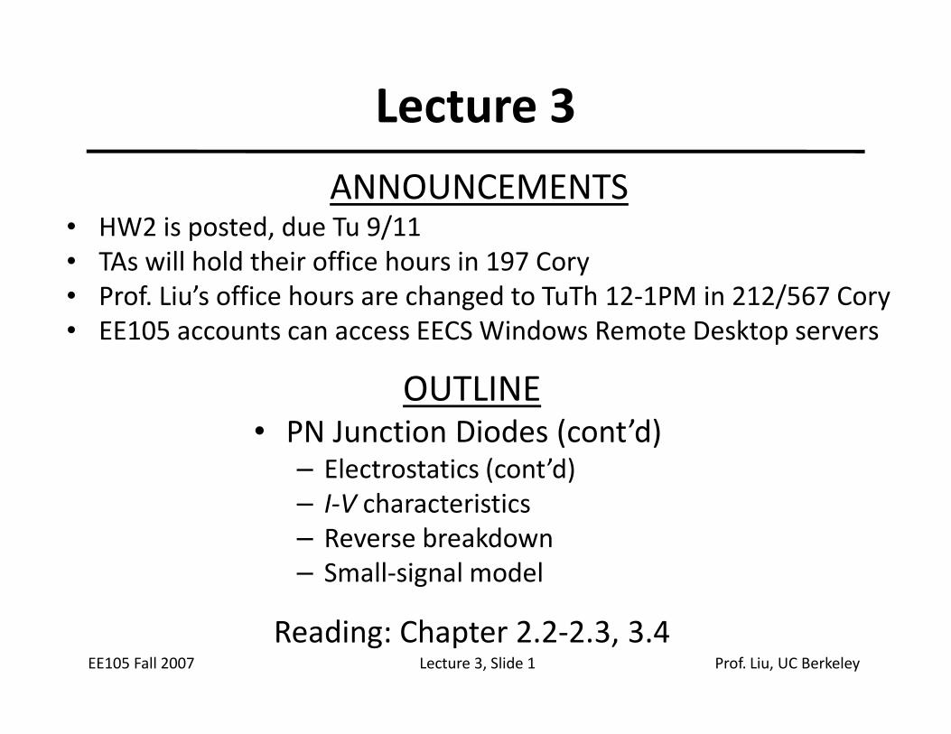
Lecture 3 ANNOUNCEMENTS • HW2 is posted, due Tu 9/11 • TAs will hold their office hours in 197 Cory • Prof. Liu’s office hours are changed to TuTh 12-1PM in 212/567 Cory • EE105 accounts can access EECS Windows Remote Desktop servers OUTLINE EE105 Fall 2007 Lecture 3, Slide 1 Prof. Liu, UC Berkeley OUTLINE • PN Junction Diodes (cont’d) – Electrostatics (cont’d) – I-V characteristics – Reverse breakdown – Small-signal model Reading: Chapter 2.2-2.3, 3.4
Transcript of Lecture 3 - University of California, Berkeleyee105/fa07/lectures/Lecture 3.pdf · Lecture 3...
Lecture 3
ANNOUNCEMENTS• HW2 is posted, due Tu 9/11
• TAs will hold their office hours in 197 Cory
• Prof. Liu’s office hours are changed to TuTh 12-1PM in 212/567 Cory
• EE105 accounts can access EECS Windows Remote Desktop servers
OUTLINE
EE105 Fall 2007 Lecture 3, Slide 1 Prof. Liu, UC Berkeley
OUTLINE• PN Junction Diodes (cont’d)
– Electrostatics (cont’d)
– I-V characteristics
– Reverse breakdown
– Small-signal model
Reading: Chapter 2.2-2.3, 3.4
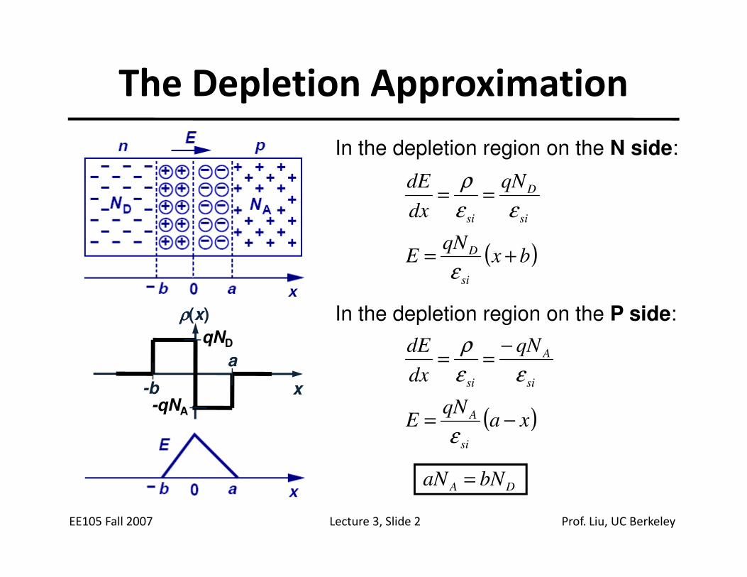
The Depletion Approximation
In the depletion region on the N side:
( )bxqN
E
qN
dx
dE
si
D
si
D
si
+=
==
ε
εε
ρ
EE105 Fall 2007 Lecture 3, Slide 2 Prof. Liu, UC Berkeley
ρρρρ(x)
x-qNA
qND
In the depletion region on the P side:
( )xaqN
E
qN
dx
dE
si
A
si
A
si
−=
−==
ε
εε
ρ
DA bNaN =
a
-b
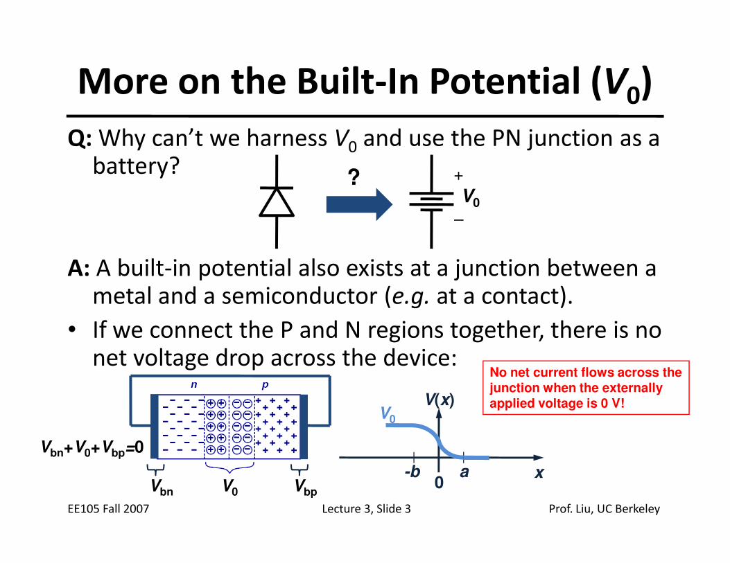
More on the Built-In Potential (V0)
Q: Why can’t we harness V0 and use the PN junction as a battery?
A: A built-in potential also exists at a junction between a metal and a semiconductor (e.g. at a contact).
+
–
V0
?
EE105 Fall 2007 Lecture 3, Slide 3 Prof. Liu, UC Berkeley
metal and a semiconductor (e.g. at a contact).
• If we connect the P and N regions together, there is no net voltage drop across the device:
VbpVbn V0
Vbn+V0+Vbp=0
V(x)
xa-b
V0
No net current flows across the junction when the externally applied voltage is 0 V!
0
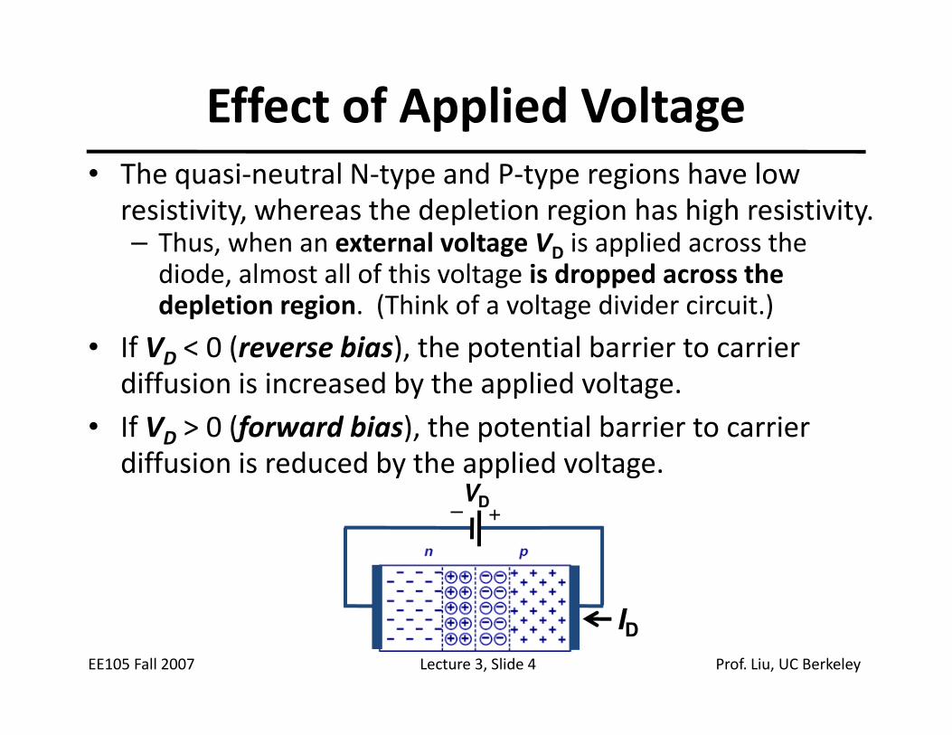
Effect of Applied Voltage
• The quasi-neutral N-type and P-type regions have low
resistivity, whereas the depletion region has high resistivity.– Thus, when an external voltage VD is applied across the
diode, almost all of this voltage is dropped across the depletion region. (Think of a voltage divider circuit.)
• If VD < 0 (reverse bias), the potential barrier to carrier
diffusion is increased by the applied voltage.
EE105 Fall 2007 Lecture 3, Slide 4 Prof. Liu, UC Berkeley
D
diffusion is increased by the applied voltage.
• If VD > 0 (forward bias), the potential barrier to carrier
diffusion is reduced by the applied voltage.VD
+–
ID
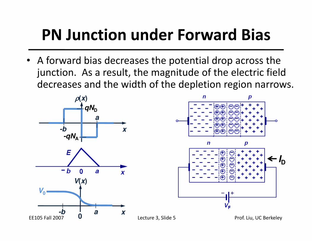
• A forward bias decreases the potential drop across the junction. As a result, the magnitude of the electric field decreases and the width of the depletion region narrows.
PN Junction under Forward Bias
ρρρρ(x)
qND
a
EE105 Fall 2007 Lecture 3, Slide 5 Prof. Liu, UC Berkeley
x-qNA
a
-b
V(x)
xa-b
V0
ID
0
Minority Carrier Injection under Forward Bias
• The potential barrier to carrier diffusion is decreased by
a forward bias; thus, carriers diffuse across the junction.
– The carriers which diffuse across the junction become minority
carriers in the quasi-neutral regions; they recombine with
majority carriers, “dying out” with distance.
EE105 Fall 2007 Lecture 3, Slide 6 Prof. Liu, UC Berkeley
np(x)
np0
A
ip
N
nn
2
0 =Equilbrium concentration of electrons on the P side:
edge of depletion regionx'
0
x'
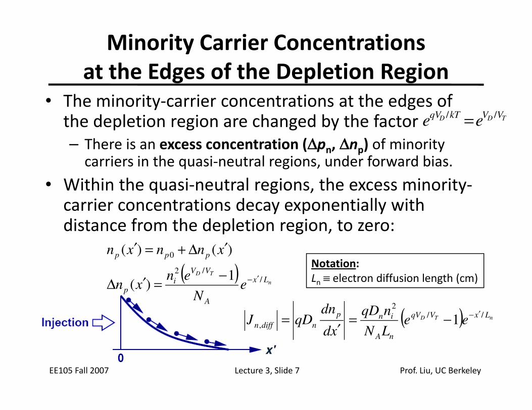
Minority Carrier Concentrations
at the Edges of the Depletion Region
• The minority-carrier concentrations at the edges of the depletion region are changed by the factor
– There is an excess concentration (∆∆∆∆pn, ∆∆∆∆np) of minority carriers in the quasi-neutral regions, under forward bias.
• Within the quasi-neutral regions, the excess minority-carrier concentrations decay exponentially with
TDD VVkTqVee
// =
EE105 Fall 2007 Lecture 3, Slide 7 Prof. Liu, UC Berkeley
carrier concentrations decay exponentially with distance from the depletion region, to zero:
( )n
TD
Lx
A
VV
ip
ppp
eN
enxn
xnnxn
//2
0
1)(
)()(
′−−=′∆
′∆+=′
x'
Notation:
Ln ≡ electron diffusion length (cm)
( ) nTD LxVqV
nA
inp
ndiffn eeLN
nqD
xd
dnqDJ
//2
, 1′−−=
′=
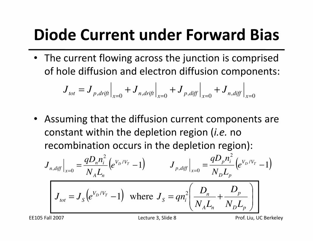
Diode Current under Forward Bias
• The current flowing across the junction is comprised
of hole diffusion and electron diffusion components:
• Assuming that the diffusion current components are
0,0,0,0, ====+++=
xdiffnxdiffpxdriftnxdriftptot JJJJJ
EE105 Fall 2007 Lecture 3, Slide 8 Prof. Liu, UC Berkeley
• Assuming that the diffusion current components are
constant within the depletion region (i.e. no
recombination occurs in the depletion region):
( ) where1 2/
+=−=
pD
p
nA
niS
VV
StotLN
D
LN
DqnJeJJ TD
( )1/
2
0, −==
TD VV
nA
in
xdiffn eLN
nqDJ ( )1
/
2
0, −==
TD VV
pD
ip
xdiffp eLN
nqDJ
Current Components under Forward Bias
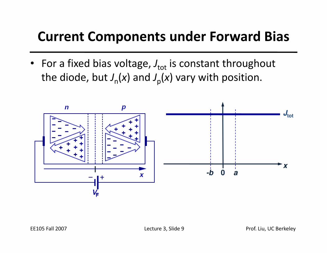
• For a fixed bias voltage, Jtot is constant throughout
the diode, but Jn(x) and Jp(x) vary with position.
Jtot
EE105 Fall 2007 Lecture 3, Slide 9 Prof. Liu, UC Berkeley
x0 a-b
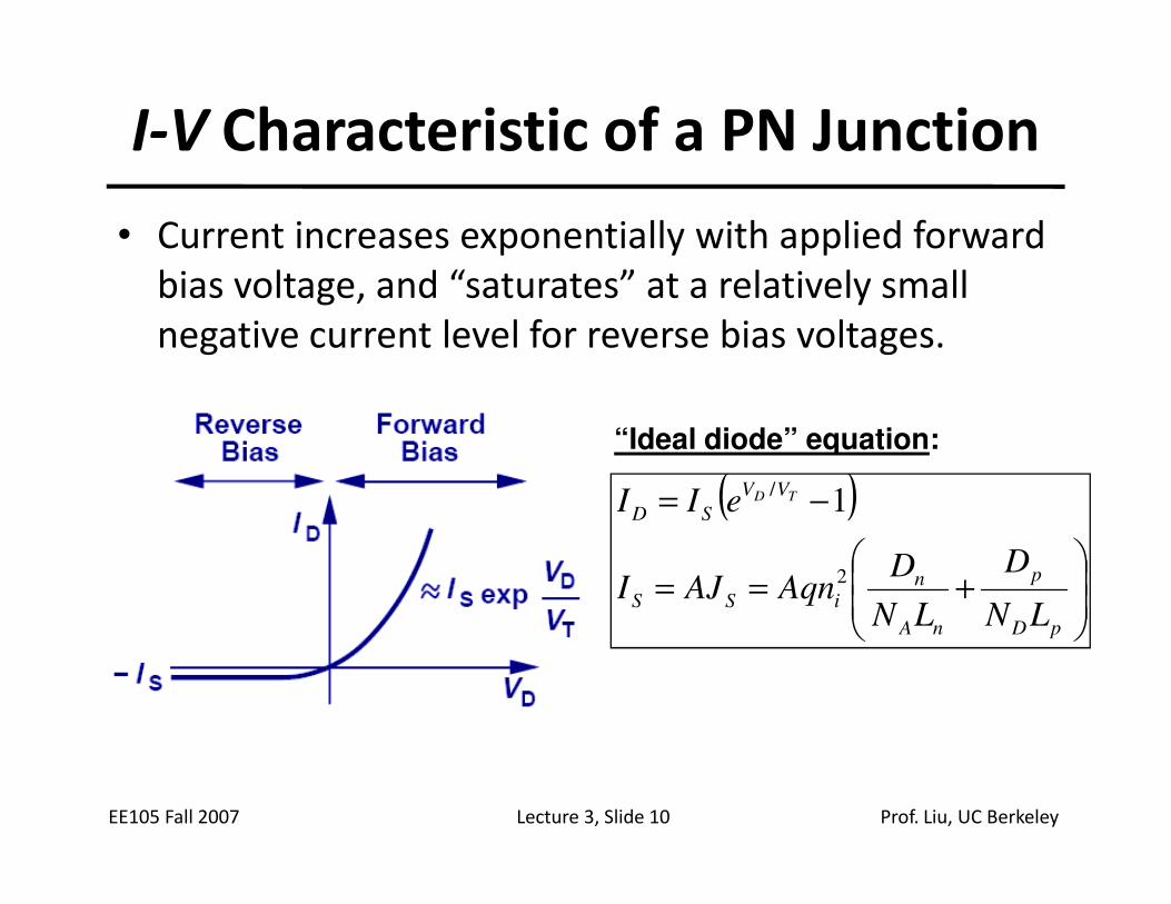
I-V Characteristic of a PN Junction
• Current increases exponentially with applied forward
bias voltage, and “saturates” at a relatively small
negative current level for reverse bias voltages.
“Ideal diode” equation:
EE105 Fall 2007 Lecture 3, Slide 10 Prof. Liu, UC Berkeley
( )
+==
−=
pD
p
nA
niSS
VV
SD
LN
D
LN
DAqnAJI
eII TD
2
/1
“Ideal diode” equation:
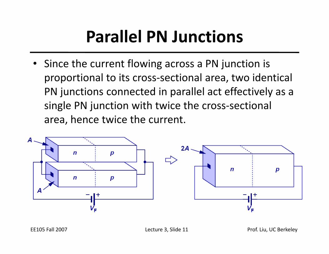
Parallel PN Junctions
• Since the current flowing across a PN junction is
proportional to its cross-sectional area, two identical
PN junctions connected in parallel act effectively as a
single PN junction with twice the cross-sectional
area, hence twice the current.
EE105 Fall 2007 Lecture 3, Slide 11 Prof. Liu, UC Berkeley
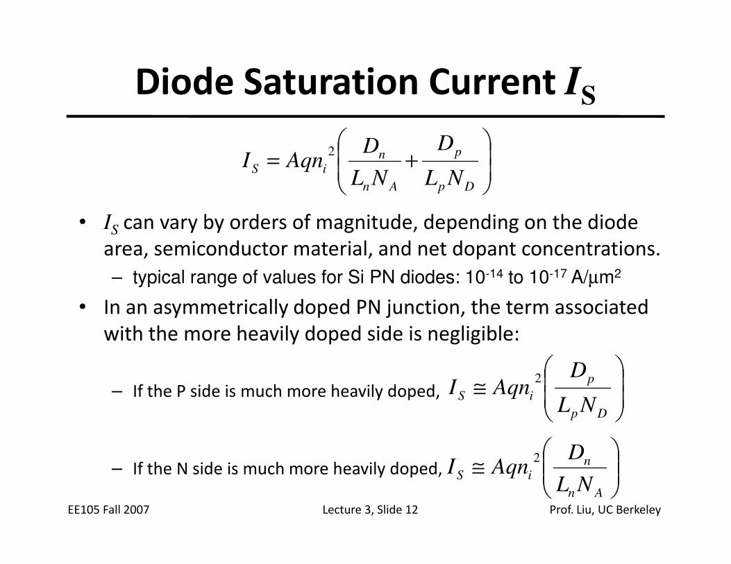
Diode Saturation Current IS
• IS can vary by orders of magnitude, depending on the diode
area, semiconductor material, and net dopant concentrations.
– typical range of values for Si PN diodes: 10-14 to 10-17 A/µm2
+=
Dp
p
An
niS
NL
D
NL
DAqnI
2
EE105 Fall 2007 Lecture 3, Slide 12 Prof. Liu, UC Berkeley
– typical range of values for Si PN diodes: 10 to 10 A/µm
• In an asymmetrically doped PN junction, the term associated
with the more heavily doped side is negligible:
– If the P side is much more heavily doped,
– If the N side is much more heavily doped,
≅
Dp
p
iSNL
DAqnI
2
≅
An
niS
NL
DAqnI
2
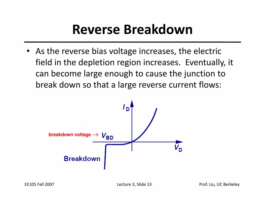
Reverse Breakdown
• As the reverse bias voltage increases, the electric
field in the depletion region increases. Eventually, it
can become large enough to cause the junction to
break down so that a large reverse current flows:
EE105 Fall 2007 Lecture 3, Slide 13 Prof. Liu, UC Berkeley
breakdown voltage
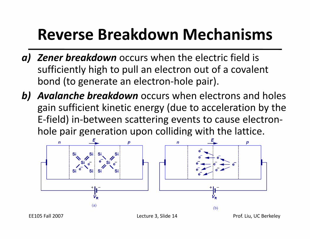
Reverse Breakdown Mechanisms
a) Zener breakdown occurs when the electric field is sufficiently high to pull an electron out of a covalent bond (to generate an electron-hole pair).
b) Avalanche breakdown occurs when electrons and holes gain sufficient kinetic energy (due to acceleration by the E-field) in-between scattering events to cause electron-
EE105 Fall 2007 Lecture 3, Slide 14 Prof. Liu, UC Berkeley
E-field) in-between scattering events to cause electron-hole pair generation upon colliding with the lattice.
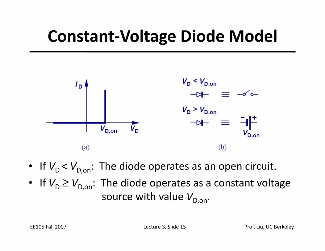
Constant-Voltage Diode Model
EE105 Fall 2007 Lecture 3, Slide 15 Prof. Liu, UC Berkeley
• If VD < VD,on: The diode operates as an open circuit.
• If VD ≥ VD,on: The diode operates as a constant voltage
source with value VD,on.
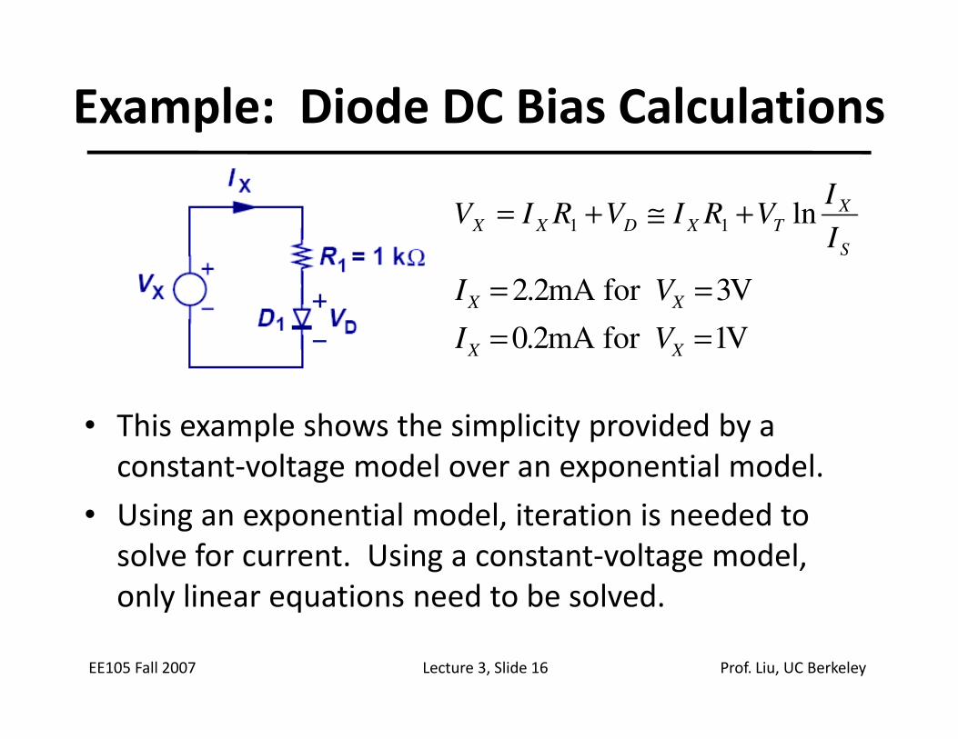
Example: Diode DC Bias Calculations
S
XTXDXX
I
IVRIVRIV ln11 +≅+=
V1for mA 2.0
V3for mA 2.2
==
==
XX
XX
VI
VI
EE105 Fall 2007 Lecture 3, Slide 16 Prof. Liu, UC Berkeley
• This example shows the simplicity provided by a
constant-voltage model over an exponential model.
• Using an exponential model, iteration is needed to
solve for current. Using a constant-voltage model,
only linear equations need to be solved.
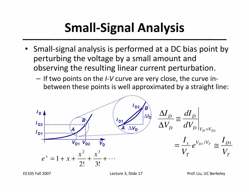
Small-Signal Analysis
• Small-signal analysis is performed at a DC bias point by perturbing the voltage by a small amount and observing the resulting linear current perturbation.
– If two points on the I-V curve are very close, the curve in-between these points is well approximated by a straight line:
EE105 Fall 2007 Lecture 3, Slide 17 Prof. Liu, UC Berkeley
T
DVV
T
s
VVD
D
D
D
V
Ie
V
I
dV
dI
V
I
TD
DD
1/1
1
≅=
≅∆
∆
=
⋅⋅⋅++++=!3!2
132
xxxe
x
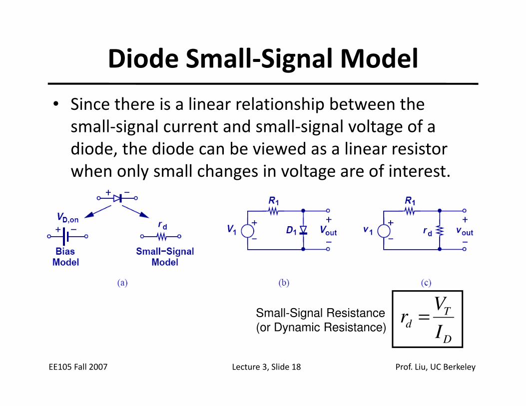
Diode Small-Signal Model
• Since there is a linear relationship between the
small-signal current and small-signal voltage of a
diode, the diode can be viewed as a linear resistor
when only small changes in voltage are of interest.
EE105 Fall 2007 Lecture 3, Slide 18 Prof. Liu, UC Berkeley
D
Td
I
Vr =Small-Signal Resistance
(or Dynamic Resistance)
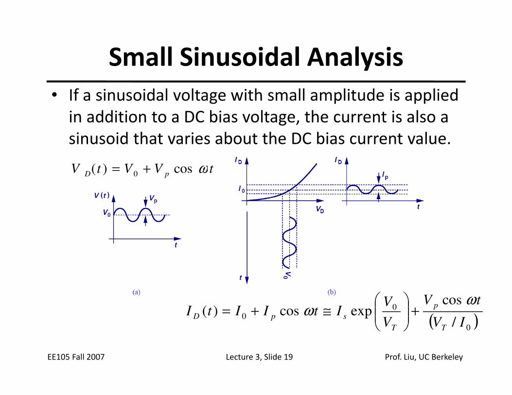
Small Sinusoidal Analysis
• If a sinusoidal voltage with small amplitude is applied
in addition to a DC bias voltage, the current is also a
sinusoid that varies about the DC bias current value.
tVVtV pD ωcos)( 0 +=
EE105 Fall 2007 Lecture 3, Slide 19 Prof. Liu, UC Berkeley
( )0
00
/
cosexpcos)(
IV
tV
V
VItIItI
T
p
T
spD
ωω +
≅+=
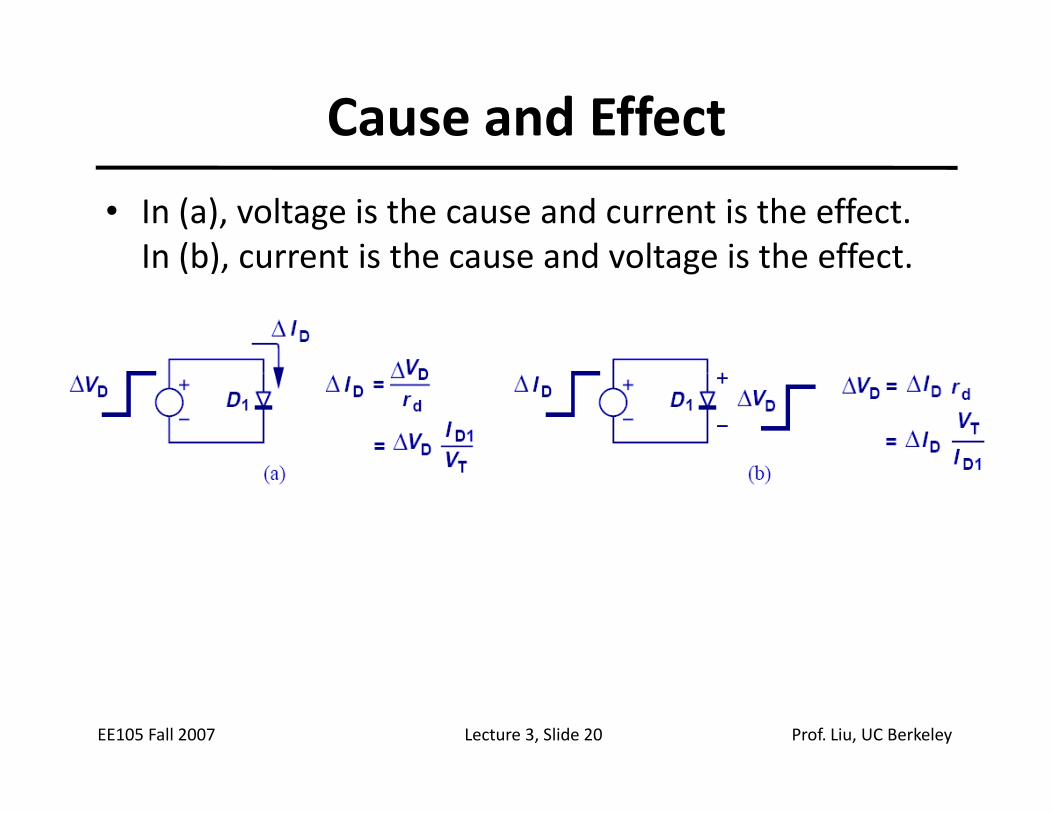
Cause and Effect
• In (a), voltage is the cause and current is the effect.
In (b), current is the cause and voltage is the effect.
EE105 Fall 2007 Lecture 3, Slide 20 Prof. Liu, UC Berkeley
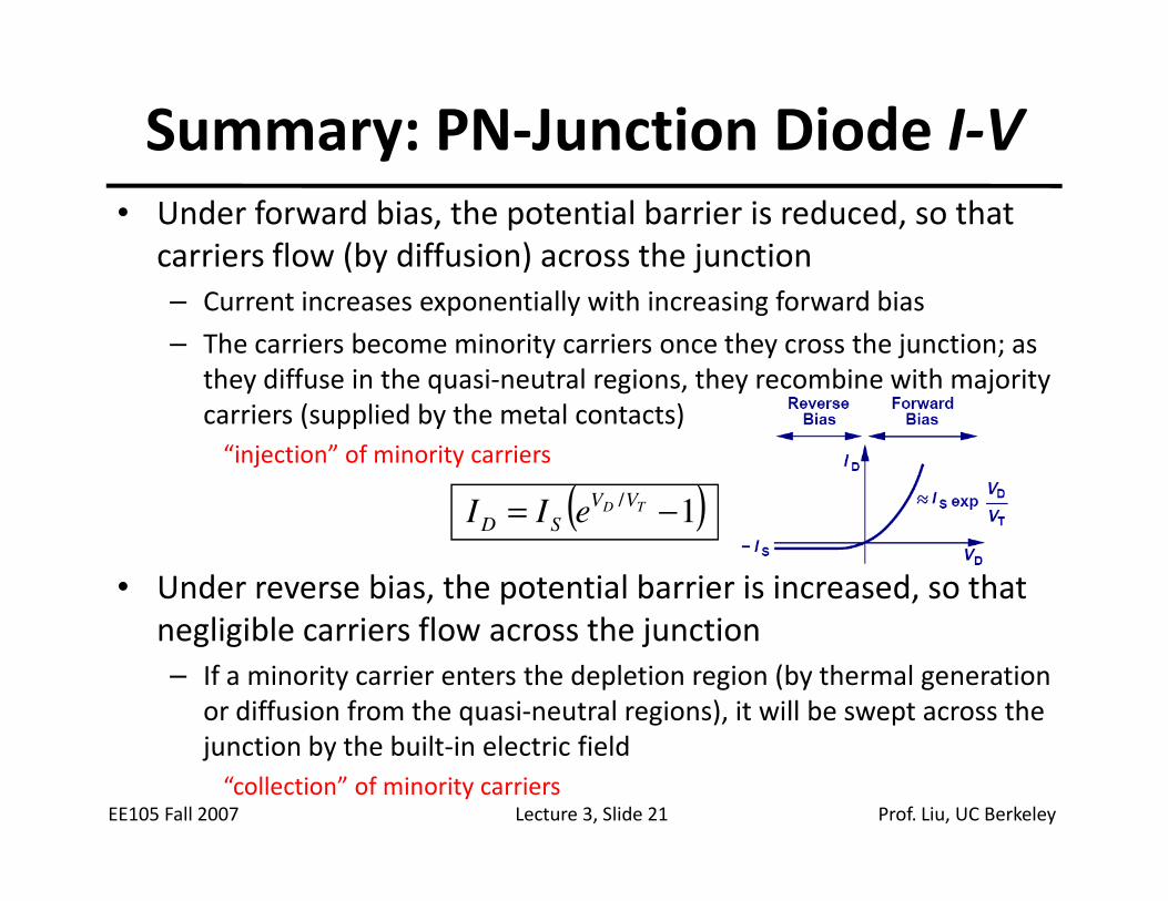
Summary: PN-Junction Diode I-V
• Under forward bias, the potential barrier is reduced, so that
carriers flow (by diffusion) across the junction
– Current increases exponentially with increasing forward bias
– The carriers become minority carriers once they cross the junction; as
they diffuse in the quasi-neutral regions, they recombine with majority
carriers (supplied by the metal contacts)
“injection” of minority carriers
EE105 Fall 2007 Lecture 3, Slide 21 Prof. Liu, UC Berkeley
“injection” of minority carriers
• Under reverse bias, the potential barrier is increased, so that
negligible carriers flow across the junction
– If a minority carrier enters the depletion region (by thermal generation
or diffusion from the quasi-neutral regions), it will be swept across the
junction by the built-in electric field
“collection” of minority carriers
( ) 1 / −= TD VV
SD eII