GOSSIP : Gas On Slimmed SIlicon Pixels NIKHEFAuke-Pieter Colijn Alessandro Fornaini Harry van der...
32
GOSSIP: Gas On Slimmed SIlicon Pixel NIKHEF Auke-Pieter Colijn Alessandro Fornaini Harry van der Graaf Peter Kluit Jan Timmermans Jan Visschers Saclay CEA DAPNIA Maximilien Chefdeville Paul Colas Yannis Giomataris Arnaud Giganon Univ. Twente/Mesa+ Jurriaan Schmitz CERN/Medipix Constm Eric Heijne Xavie Llopart Michael Campbell Thanks to: Wim Gotink Joop Rovenkamp
-
Upload
nickolas-merritt -
Category
Documents
-
view
214 -
download
0
Transcript of GOSSIP : Gas On Slimmed SIlicon Pixels NIKHEFAuke-Pieter Colijn Alessandro Fornaini Harry van der...

GOSSIP: Gas On Slimmed SIlicon Pixels
NIKHEF Auke-Pieter ColijnAlessandro FornainiHarry van der GraafPeter KluitJan TimmermansJan Visschers
Saclay CEA DAPNIA Maximilien Chefdeville Paul ColasYannis GiomatarisArnaud Giganon
Univ. Twente/Mesa+ Jurriaan Schmitz
CERN/Medipix Constm Eric HeijneXavie LlopartMichael Campbell Thanks to:
Wim GotinkJoop Rovenkamp

Cathode foil
Gem foils
Support plate
Medipix 2
Drift Space
The MediPix2 pixel CMOS chip
We apply the ‘naked’ MediPix2 chipwithout X-ray convertor!

MediPix2 pixel sensorBrass spacer blockPrinted circuit boardAluminum base plate
Micromegas
Cathode (drift) plane
55Fe
Baseplate
Drift space: 15 mm
Very strong E-field above (CMOS) MediPix!


We always knew, but never saw: the conversion of 55Fe quanta in Ar gas
No source, 1sNo source, 1s5555Fe, 1sFe, 1s
5555Fe, 10sFe, 10s
Friday 13 (!) Feb 2004: signals from a 55Fe source (220 e- per photon); 300 m x 500 m clouds as expected
14 mm
The Medipix CMOS chip facesan electric field of 350 V/50 μm
= 7 kV/mm !!

Eff = e-Thr/G
Thr: threshold setting (#e-)G: Gas amplification
Single electron efficiency
0.00
0.20
0.40
0.60
0.80
1.00
0 1000 2000 3000 4000
Threshold setting (number of electrons)
Eff
icie
ncy
(-)
G=500
G=1000
g=2000
g=4000
g=8000
Expon. (G=500)
Expon. (G=1000)
Expon. (g=2000)
Expon. (g=4000)
Expon. (g=8000)
single-electron avalanche distribution
0
0.0005
0.001
0.0015
0.002
0 1000 2000 3000 4000
electrons in avalanche
Pro
b(n
)
G=500
G=1000
G=2000
G=4000
G=8000
Expon. (G=500)
Expon. (G=1000)
Expon. (G=2000)
Expon. (G=4000)
Expon. (G=8000)Prob(n) = 1/G . e-n/G
• no attachment• homogeneous field in avalanche gap• low gas gain• simple exponential grown of avalanche
No Curran or Polyadistributions but simply:
Single electron efficiency

New trial: NIKHEF, March 30 – April 2, 2004Essential: try to see single electrons from cosmic muons (MIPs)
Pixel preamp threshold: 3000 e- (due to X-talk)Required gain: 5000 – 10.000
New MedipixNew Micromegas
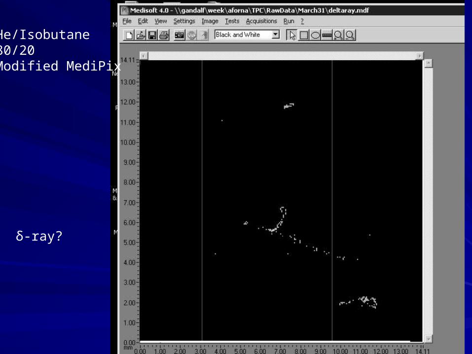
Gas: He/Isobutane 80/20 !Gain up to 30 k!He/CF4 80/20
…… It Works!

He/Isobutane80/20Modified MediPix
Sensitive area:14 x 14 x 15 mm3
Drift direction:Verticalmax = 15 mm

He/Isobutane80/20Modified MediPix

He/Isobutane80/20Modified MediPix

He/Isobutane80/20Non ModifiedMediPix
Americium Source

He/Isobutane80/20Modified MediPix
He/Isobutane80/20Modified MediPix
δ-ray?

MediPix modified by MESA+, Univ. of Twente, The Netherlands
Pixel Pitch: 55 x 55 μm2
Bump Bond pad: 25 μm octagonal75 % surface: pacivation SiNNew Pixel Pad: 45 x 45 μm2
Insulating surface was 75 %Reduced to 20 %
Non Modified Modified

Non Modified Modified
Peter Kluit: cluster & electron density versus MC of MIP cosmic rays:single electron efficiency > 0.95AND:Good explanation for Moire effect: pitch Micromegas holes: 60 μm
pitch MediPix pixels: 55 μmPeriodic position of hole w.r.t. pixel: repeats after 12 pixels!

Modified
Non Modified
InGrid: perfect alignment of pixels and grid holes!Small pad: small capacitance!

Integrate GEM/Micromegas and pixel sensor
‘GEM’ ‘Micromegas’
By ‘wafer post processing’
InGrid

First InGrid expected in July
Wafer dia.: 100 mm30 fields with variety of pillar geometry

1. WSLC-Paris 2004: LC ready in 2015…, not known where…..2. People with power and $: what is the relevance for LHC?!
So:
Other applications of TimePixGrid:
- μ-TPC- upgrades of TPCs: STAR, ALICE- Transition Radiation Detectors- GOSSIP: tracker for intense radiation environment

CMOS pixel array
MIP
Micromegas
GOSSIP: Gas On Slimmed SIlicon Pixels
Drift gap: 1 mmMax drift time: 10 ns
MIP
CMOS pixel chip
Cathode foil

Essentials of GOSSIP:
• Generate charge signal in gas instead of Si (e-/ions versus e-/holes)•Amplify # electrons in gas (electron avalanche versus FET preamps)
Then:• No radiation damage in depletion layer or pixel preamp FETs• No power dissipation of preamp FETs
GOSSIP: 1 mm gas layer + 20 μm gain gap + CMOS (digital!) chipAfter all: it is a TPC with 1 mm drift length (parallax!)
Max. drift length: 1 mmMax. drift time: 10 nsResolution: 0.1 mm 1 ns

EfficiencyPosition resolutionRate effectsAgeingRadiation hardnessHV breakdownsPower dissipationMaterial budget

Efficiency
Single electron efficiency: > 0.95Number of clusters per mm: 3 (Ar) – 10 (Isobutane)Number of electrons per cluster: 3 (Ar) - ? (Isobutane)Probability to have 1 cluster in 1 mm Ar: 0.95
With nice gas: eff ~ 0.99 in 1 mm thick layer should be possible
But…….
• Parallax error due to 1 mm thick layer, with 3rd coordinate 0.1 mm:• TPC/ max drift time 10 ns / σ = 0.1 mm / σ = 1 ns (not easy….)• Lorentz angle
• We want light ions (rate effect), and little UV photon induced avalanches

Position resolutionTransversal coordinateslimited by:• pixel dimensions: 20 x 20 – 50 x 50 μm2
Note: we MUST have pixels: no strips (pad capacity/noise)Good resolution in non-bending plane!Pixel number has NO cost consequence (m2 Si counts)Pixel number has some effect on CMOS power dissipation
• Diffusion: max. drift length 1 mm: little effect (?)
• δ-rays
Drift coordinatelimited by:• Pulse height fluctuation
• gas gain (3 k), pad capacity, # e- per cluster
0
Q
20 – 50 ns

Rate effects
time
0
Q
20 – 50 ns
• only (average) ~10 e- per track• gas gain only 3 k• most ions are discharged at grid after traveling time of 20 – 50 ns• a few percent enter the drift space:
LHC @ max lumi:@ 2 cm from beam pipe:10 tracks cm-2 25 ns-1
400 MHz cm-2!
Some ions crossing drift space: takes 20 – 200 μs!• B-field should help• ion space charge has NO effect on gas gain• ion charge may influence drift field, but this does little harm• ion charge may influence drift direction (?)• Recombination?

AgeingRemember the MSGCs……
Little ageing:
• the ratio (anode surface)/(gas volume) is very high w.r.t. i.e. MDTs• little gas gain (3k)• homogeneous drift field + homogeneous multiplication field versus 1/R field of wire. Absence of high E-field close to a wire: no high electron energy; little production of chemical radicals
Confirmed by measurements (Alfonsi, Colas)

Radiation hardness
• CMOS 130 nm technology: OK up to ? rad• need only modest input FETs

HV breakdowns
4 Protection Network
1 High-resistive layer
2 High-resistive layer
3 ‘massive’ pads

Power dissipation
MediPix2: 1 W/cm2 preamp powerLarge part in preamps + 2 discr per pixel
For GOSSIP CMOS Pixel chip:
- Array of 512 x 512 monostable gates- Row OR, Column OR, decoders, TimeStamp, shift registers
10 M transistors, most in rest Gas Cooling feasible!

Material budget
‘Slimmed’ Si CMOS chip: 30 μm SiPixel resistive layer 5 μm SiN2
Anode pads 5 μm AlGrid 1 μm AlGrid resistive layer 5 μm SiN2Cathode 1 μm Al
CF string support, gas tubing, power

How to proceed?
- InGrid 1 available for tests in July:- rate effects (all except change in drift direction)- ageing
Proof-of-principle of signal generator: Xmas 2004!
- InGrid 2: HV breakdowns, beamtests with MediPix (TimePix1 in 2005)- TimePix2: CMOS chip for GOSSIP: CERN MediPix/ATLAS Pixel
Needed: calculations/simulations:- PhD student- students- (NIKHEF) vertex experts: i.e. Henk T, Els K, Nigel H, Jos S, Marcel D.