Flip-Flops...Flip-Flops Outline: 1. Timing noise ÆSignal races, glitches ÆFPGA example...
41
Flip Flip - - Flops Flops Outline: Outline: 1. 1. Timing noise Timing noise Signal races, glitches FPGA example (“assign” bad) 2. 2. Synchronous circuits and memory Synchronous circuits and memory Logic gate example 3. 3. Flip Flip - - Flop memory Flop memory RS-latch example 4. 4. D and JK flip D and JK flip - - flops flops Flip-flops in FPGAs 5. Synchronous circuit design with Synchronous circuit design with FPGAs FPGAs FPGA example (“always” good). Parallel circuit design with FPGAs.
Transcript of Flip-Flops...Flip-Flops Outline: 1. Timing noise ÆSignal races, glitches ÆFPGA example...
FlipFlip--FlopsFlopsOutline:Outline:
1.1. Timing noiseTiming noise
Signal races, glitches
FPGA example (“assign” bad)
2.2. Synchronous circuits and memorySynchronous circuits and memory
Logic gate example
3.3. FlipFlip--Flop memoryFlop memory
RS-latch example
4.4. D and JK flipD and JK flip--flopsflops
Flip-flops in FPGAs
5. Synchronous circuit design with Synchronous circuit design with FPGAsFPGAs
FPGA example (“always” good).
Parallel circuit design with FPGAs.
Timing noiseTiming noise
Amplitude NoiseAmplitude NoiseA digital circuit is very immune to amplitude noise, since it can only have
two values (Low or High, True or False, 0 or 1). Digital electronics circuits typically have error rates smaller than 1 part in 109.
Timing NoiseTiming NoiseJust like an analog circuit, a digital circuit can experience timing noise.
Fortunately, good clocks are cheap and easily available, and a good design will eliminate the effects of timing noise.
If attention is not paid to timing issues can easily produce amplitude noise (bit errors).

Signal RaceSignal RaceThe timing delays produced by wires and logic gates can produce unwanted (illogical) outputs.
Example: 3-input NAND gateAB
CY
AB
A
B
C
ideal Y
TimeTime
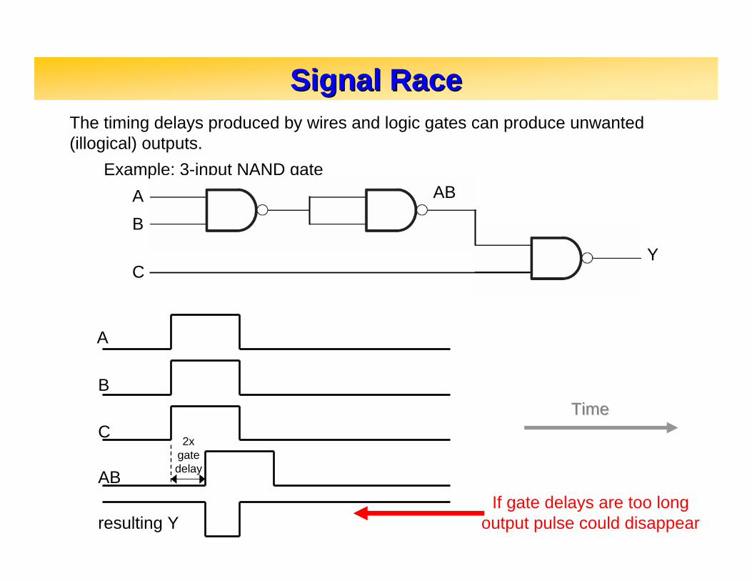
Signal RaceSignal RaceThe timing delays produced by wires and logic gates can produce unwanted (illogical) outputs.
Example: 3-input NAND gateAB
CY
AB
A
B
C
AB
resulting Y
TimeTime
2xgatedelay
If gate delays are too longoutput pulse could disappear
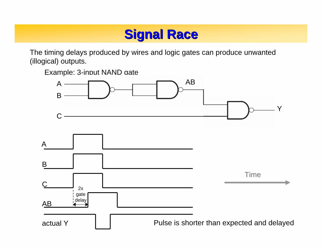
Signal RaceSignal RaceThe timing delays produced by wires and logic gates can produce unwanted (illogical) outputs.
Example: 3-input NAND gateAB
CY
AB
A
B
C
AB
actual Y
TimeTime
2xgatedelay
Pulse is shorter than expected and delayed
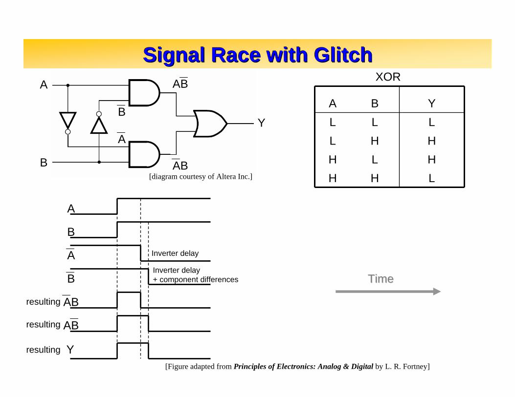
Signal Race with GlitchSignal Race with Glitch
LHHHLHHHLLLLYBA
XOR
[diagram courtesy of Altera Inc.]
A
B
A
B
BA
AB
Y
TimeTime
A
B
A
B
AB
BA
Y
resulting
resulting
resulting
Inverter delay
Inverter delay+ component differences
[Figure adapted from Principles of Electronics: Analog & Digital by L. R. Fortney]
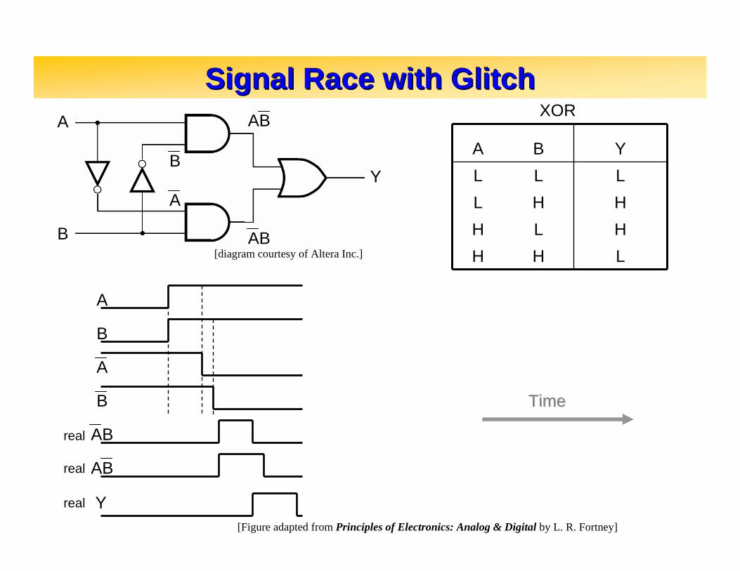
Signal Race with GlitchSignal Race with Glitch
LHHHLHHHLLLLYBA
XOR
[diagram courtesy of Altera Inc.]
A
B
A
B
BA
AB
Y
TimeTime
A
B
A
B
AB
BA
Y
real
real
real
[Figure adapted from Principles of Electronics: Analog & Digital by L. R. Fortney]
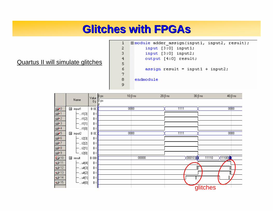
Glitches with Glitches with FPGAsFPGAs
glitches
Quartus II will simulate glitches

Asynchronous DesignAsynchronous Design
Asynchronous designAsynchronous design requires very careful attention to signal delays to avoid producing glitches and other spurious signals.
GlitchesGlitches will produce false data and can produce very wrong results
e.g. a glitch on the most-significant-bit will produce a factor of 2 error.
Asynchronous design can produce very fast digital circuits, but is generally avoided due to more difficult design.Asynchronous design can produce very fast digital circuits, but is generally avoided due to more difficult design.
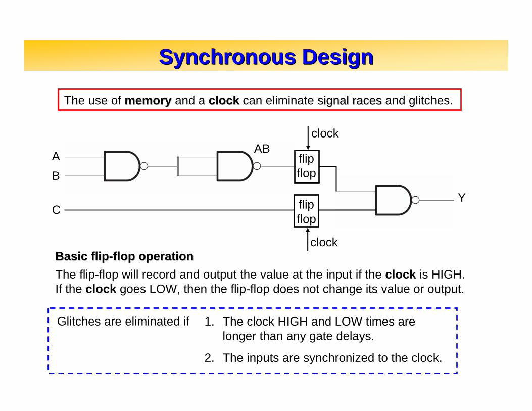
Synchronous DesignSynchronous Design
The use of memorymemory and a clockclock can eliminate signal racessignal races and glitches.
AB
CY
ABclock
clock
flipflop
flipflop
Basic flipBasic flip--flop operationflop operationThe flip-flop will record and output the value at the input if the clock is HIGH. If the clock goes LOW, then the flip-flop does not change its value or output.
Glitches are eliminated if 1. The clock HIGH and LOW times are longer than any gate delays.
2. The inputs are synchronized to the clock.
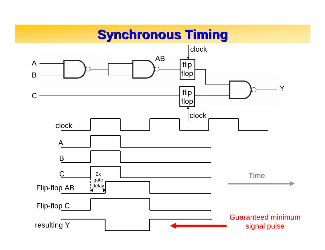
Synchronous TimingSynchronous Timing
AB
CY
ABclock
clock
flipflop
flipflop
A
B
C
Flip-flop AB
resulting Y
2xgatedelay
TimeTime
clock
Flip-flop CGuaranteed minimum
signal pulse
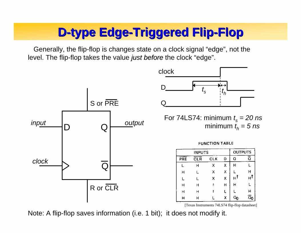
DD--type Edgetype Edge--Triggered FlipTriggered Flip--FlopFlopGenerally, the flip-flop is changes state on a clock signal “edge”, not the
level. The flip-flop takes the value just beforejust before the clock “edge”.
[Texas Instruments 74LS74 flip-flop datasheet]
Note: A flip-flop saves information (i.e. 1 bit); it does not modify it.
clock
D
Q
ts th
For 74LS74: minimum ts = 20 nsminimum th = 5 nsD
clock
Q
Q
R or CLR
S or PRE
input output
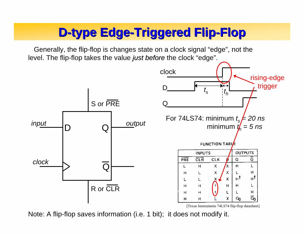
rising-edgetrigger
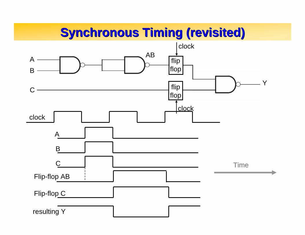
Synchronous Timing (revisited)Synchronous Timing (revisited)
AB
CY
ABclock
clock
flipflop
flipflop
A
B
C
Flip-flop AB
resulting Y
TimeTime
clock
Flip-flop C
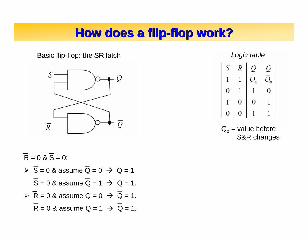
How does a flipHow does a flip--flop work?flop work?Basic flip-flop: the SR latch Logic table
Q0 = value beforeS&R changes
R = 0 & S = 0:
S = 0 & assume Q = 0 Q = 1.
S = 0 & assume Q = 1 Q = 1.
R = 0 & assume Q = 0 Q = 1.
R = 0 & assume Q = 1 Q = 1.
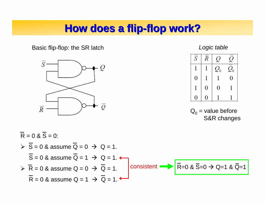
How does a flipHow does a flip--flop work?flop work?Basic flip-flop: the SR latch Logic table
Q0 = value beforeS&R changes
R = 0 & S = 0:
S = 0 & assume Q = 0 Q = 1.
S = 0 & assume Q = 1 Q = 1.
R = 0 & assume Q = 0 Q = 1.
R = 0 & assume Q = 1 Q = 1.
consistent R=0 & S=0 Q=1 & Q=1
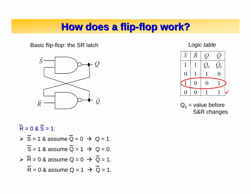
How does a flipHow does a flip--flop work?flop work?Basic flip-flop: the SR latch Logic table
Q0 = value beforeS&R changes
R = 0 & S = 1:R = 0 & S = 1:
S = 1 & assume Q = 0 Q = 1.
S = 1 & assume Q = 1 Q = 0.
R = 0 & assume Q = 0 Q = 1.
R = 0 & assume Q = 1 Q = 1.
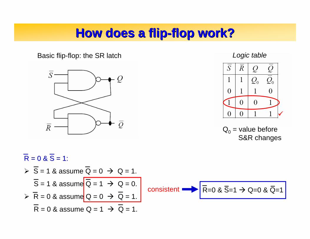
How does a flipHow does a flip--flop work?flop work?Basic flip-flop: the SR latch Logic table
Q0 = value beforeS&R changes
R = 0 & S = 1:R = 0 & S = 1:
S = 1 & assume Q = 0 Q = 1.
S = 1 & assume Q = 1 Q = 0.
R = 0 & assume Q = 0 Q = 1.
R = 0 & assume Q = 1 Q = 1.
consistent R=0 & S=1 Q=0 & Q=1
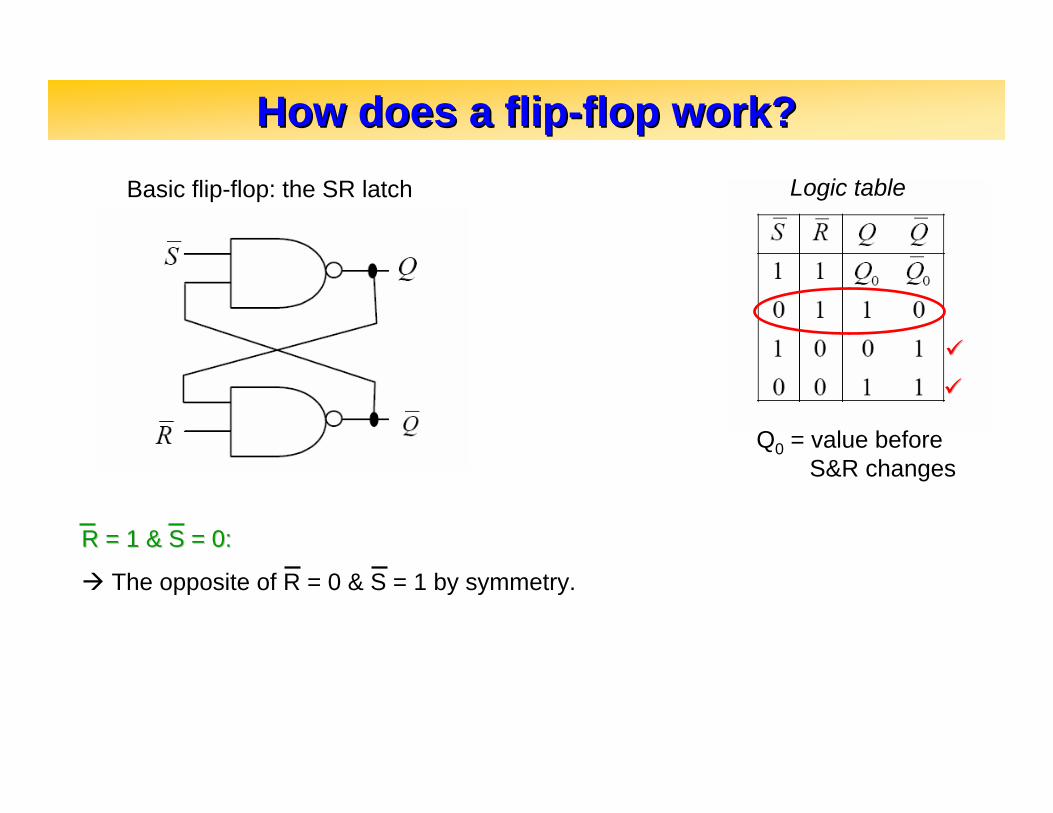
How does a flipHow does a flip--flop work?flop work?Basic flip-flop: the SR latch Logic table
Q0 = value beforeS&R changes
R = 1 & S = 0:R = 1 & S = 0:
The opposite of R = 0 & S = 1 by symmetry.
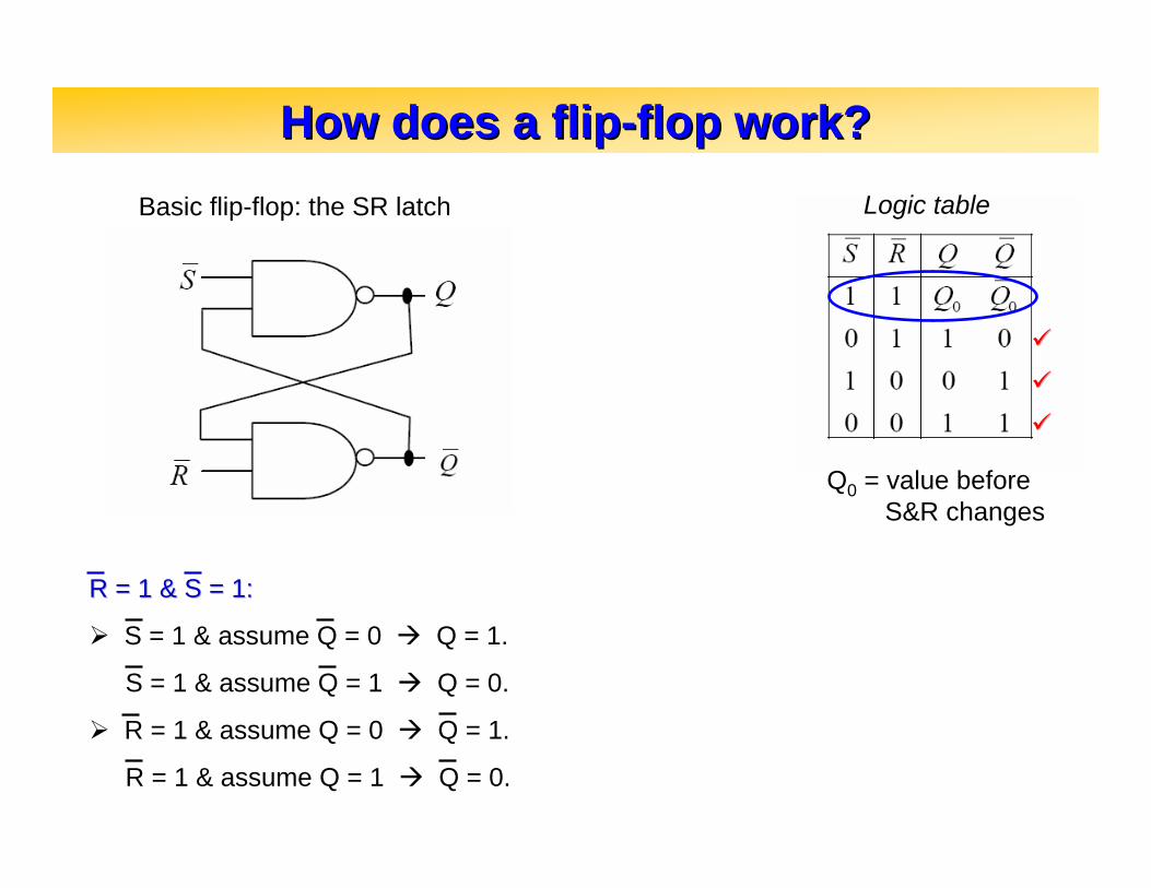
How does a flipHow does a flip--flop work?flop work?Basic flip-flop: the SR latch Logic table
Q0 = value beforeS&R changes
R = 1 & S = 1:R = 1 & S = 1:
S = 1 & assume Q = 0 Q = 1.
S = 1 & assume Q = 1 Q = 0.
R = 1 & assume Q = 0 Q = 1.
R = 1 & assume Q = 1 Q = 0.
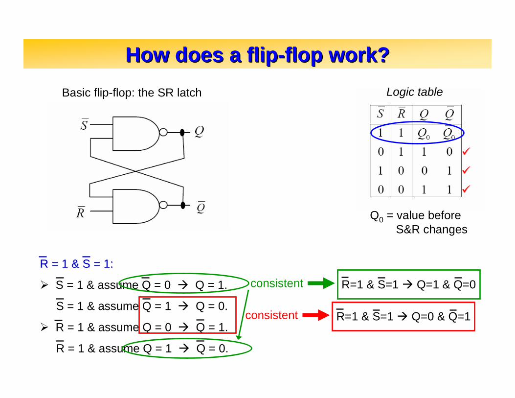
How does a flipHow does a flip--flop work?flop work?Basic flip-flop: the SR latch Logic table
Q0 = value beforeS&R changes
R = 1 & S = 1:R = 1 & S = 1:
S = 1 & assume Q = 0 Q = 1.
S = 1 & assume Q = 1 Q = 0.
R = 1 & assume Q = 0 Q = 1.
R = 1 & assume Q = 1 Q = 0.
consistent R=1 & S=1 Q=0 & Q=1
consistent R=1 & S=1 Q=1 & Q=0
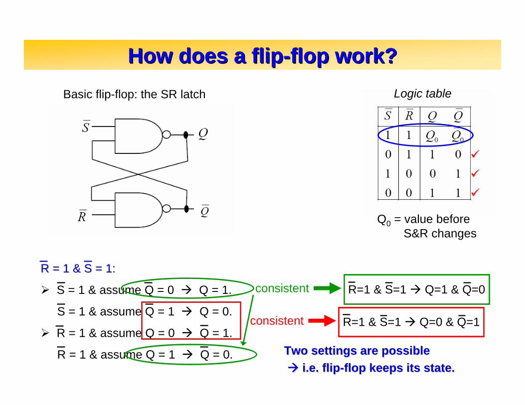
Two settings are possibleTwo settings are possiblei.e. flipi.e. flip--flop keeps its state.flop keeps its state.
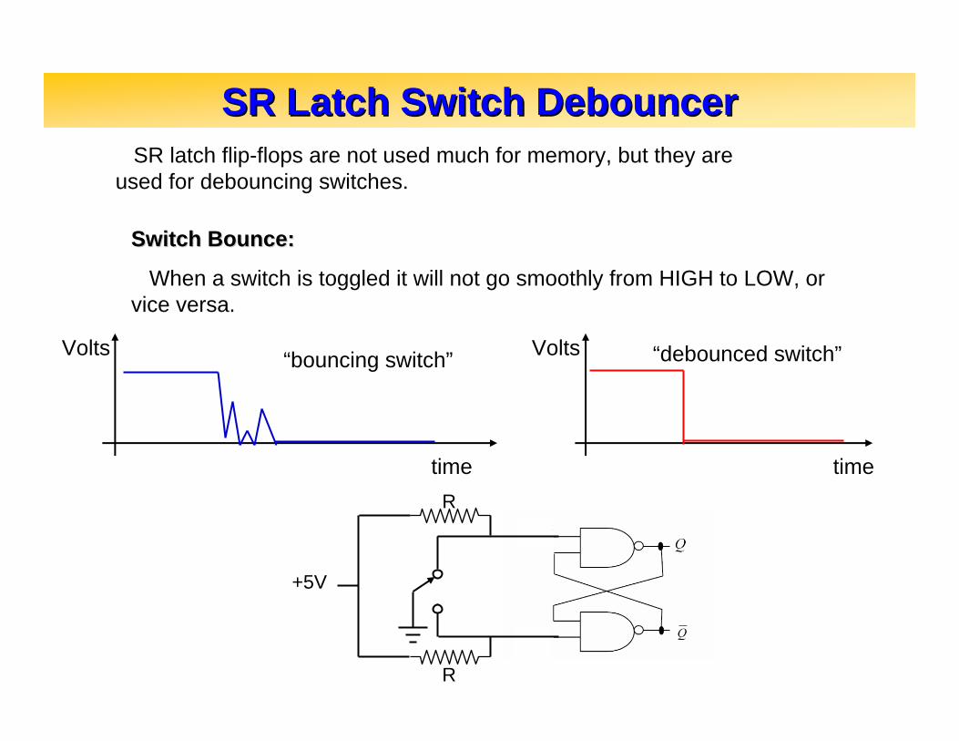
SR Latch Switch SR Latch Switch DebouncerDebouncerSR latch flip-flops are not used much for memory, but they are
used for debouncing switches.
Switch Bounce:Switch Bounce:
When a switch is toggled it will not go smoothly from HIGH to LOW, or vice versa.
time
Volts Volts
time
“bouncing switch” “debounced switch”
+5V
R
R
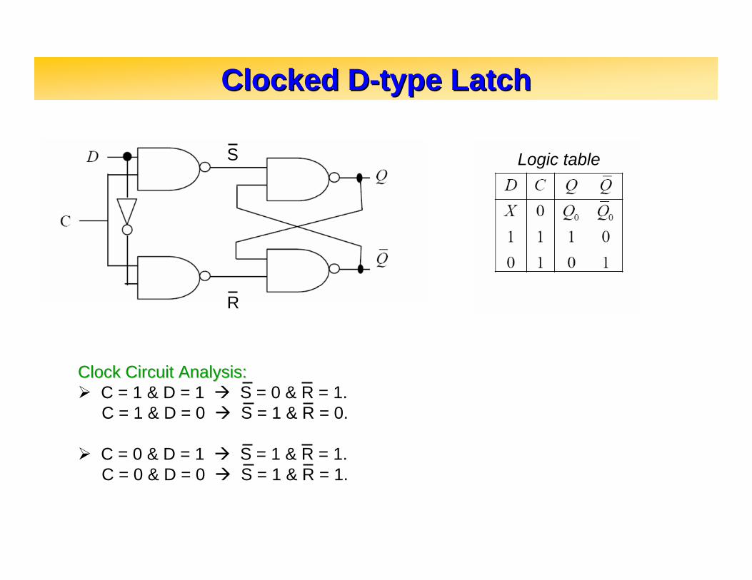
Clocked DClocked D--type Latchtype Latch
Logic tableS
R
Clock Circuit Analysis:Clock Circuit Analysis:C = 1 & D = 1 S = 0 & R = 1.C = 1 & D = 0 S = 1 & R = 0.
C = 0 & D = 1 S = 1 & R = 1.C = 0 & D = 0 S = 1 & R = 1.
Clocked DClocked D--type Latchtype Latch
Logic tableS
R
Clock Circuit Analysis:Clock Circuit Analysis:C = 1 & D = 1 S = 0 & R = 1.C = 1 & D = 0 S = 1 & R = 0.
C = 0 & D = 1 S = 1 & R = 1.C = 0 & D = 0 S = 1 & R = 1.
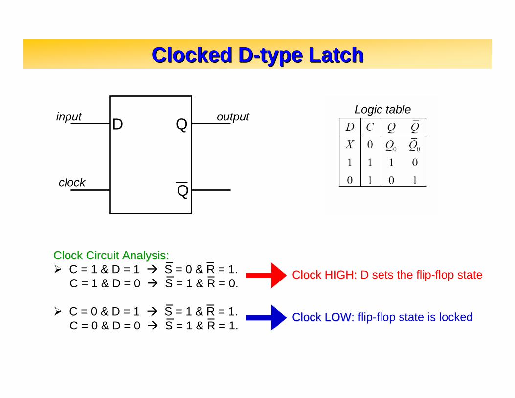
Clock HIGH:Clock HIGH: D sets the flip-flop state
Clock LOW:Clock LOW: flip-flop state is locked
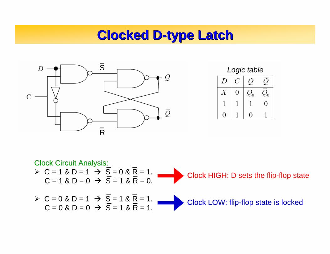
Clocked DClocked D--type Latchtype Latch
Logic table
Clock Circuit Analysis:Clock Circuit Analysis:C = 1 & D = 1 S = 0 & R = 1.C = 1 & D = 0 S = 1 & R = 0.
C = 0 & D = 1 S = 1 & R = 1.C = 0 & D = 0 S = 1 & R = 1.
Clock HIGH:Clock HIGH: D sets the flip-flop state
Clock LOW:Clock LOW: flip-flop state is locked
D
clock
Q
Q
input output
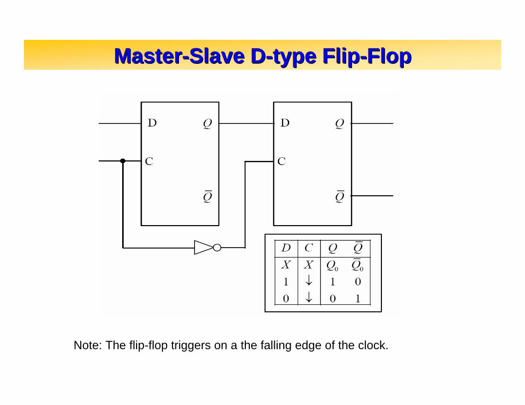
MasterMaster--Slave DSlave D--type Fliptype Flip--FlopFlop
Note: The flip-flop triggers on a the falling edge of the clock.
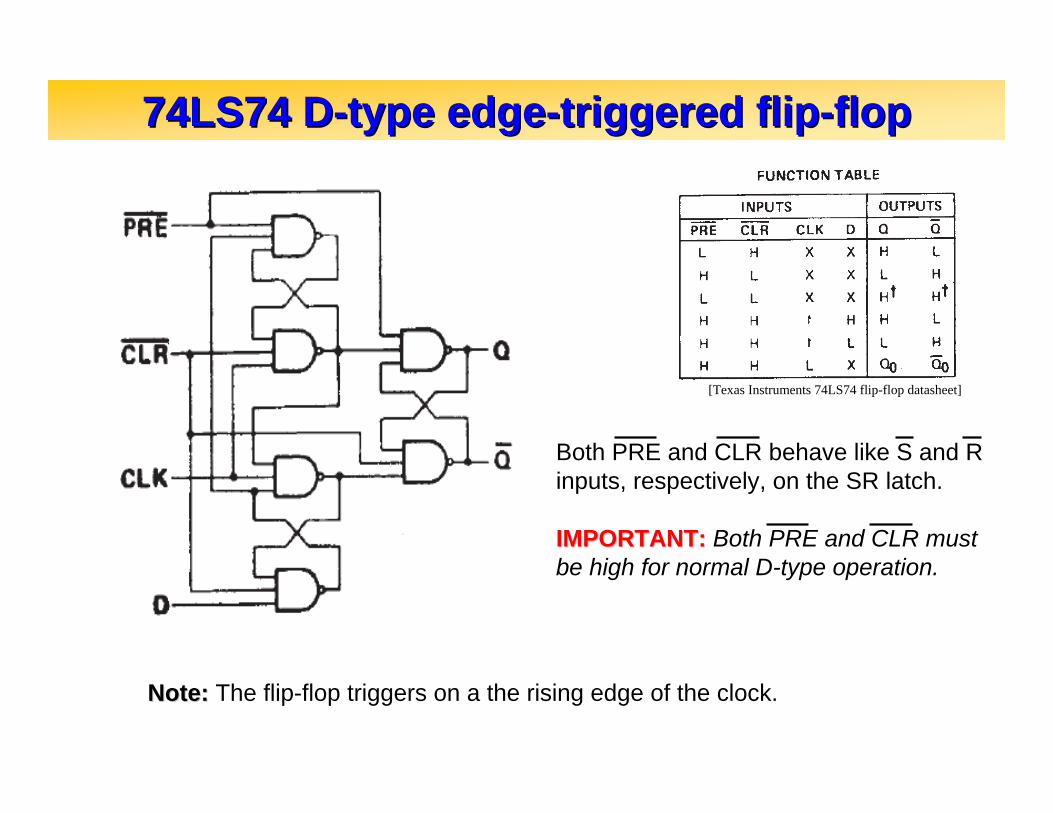
74LS74 D74LS74 D--type edgetype edge--triggered fliptriggered flip--flopflop
Note:Note: The flip-flop triggers on a the rising edge of the clock.
[Texas Instruments 74LS74 flip-flop datasheet]
Both PRE and CLR behave like S and R inputs, respectively, on the SR latch.
IMPORTANT:IMPORTANT: Both PRE and CLR must be high for normal D-type operation.
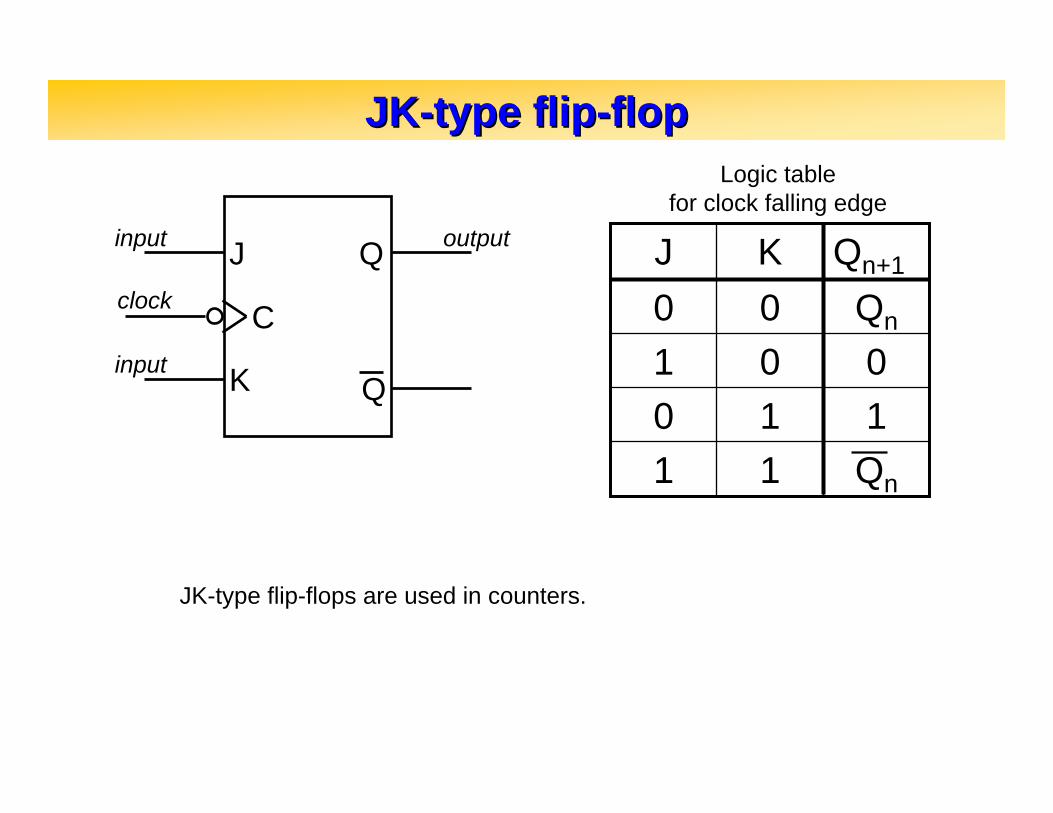
JKJK--type fliptype flip--flopflop
Jclock
Q
Q
input output
Kinput
C
Qn11110001
Qn00Qn+1KJ
Logic tablefor clock falling edge
JK-type flip-flops are used in counters.
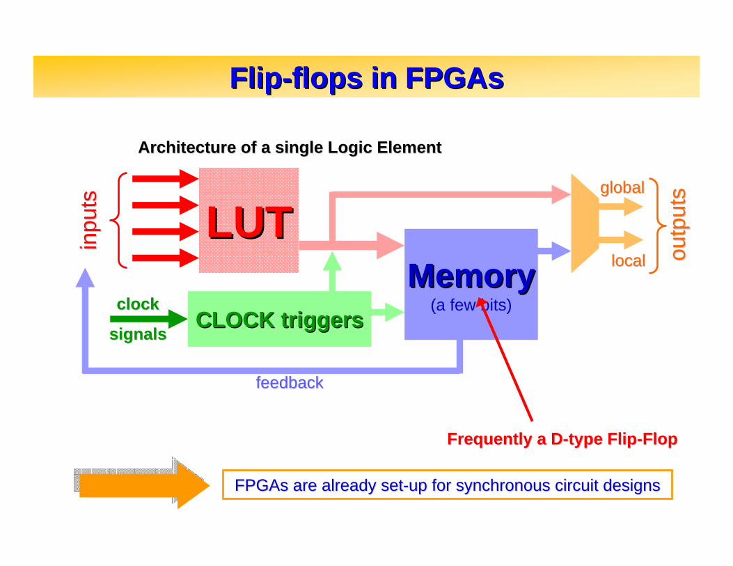
FlipFlip--flops in flops in FPGAsFPGAs
LUTLUTinpu
tsin
puts
MemoryMemory(a few bits)
CLOCK triggersCLOCK triggersclockclock
signalssignals
globalglobal
locallocal outp
uts
outp
uts
feedbackfeedback
Architecture of a single Logic ElementArchitecture of a single Logic Element
Frequently a DFrequently a D--type Fliptype Flip--FlopFlop
FPGAsFPGAs are already setare already set--up for synchronous circuit designsup for synchronous circuit designs
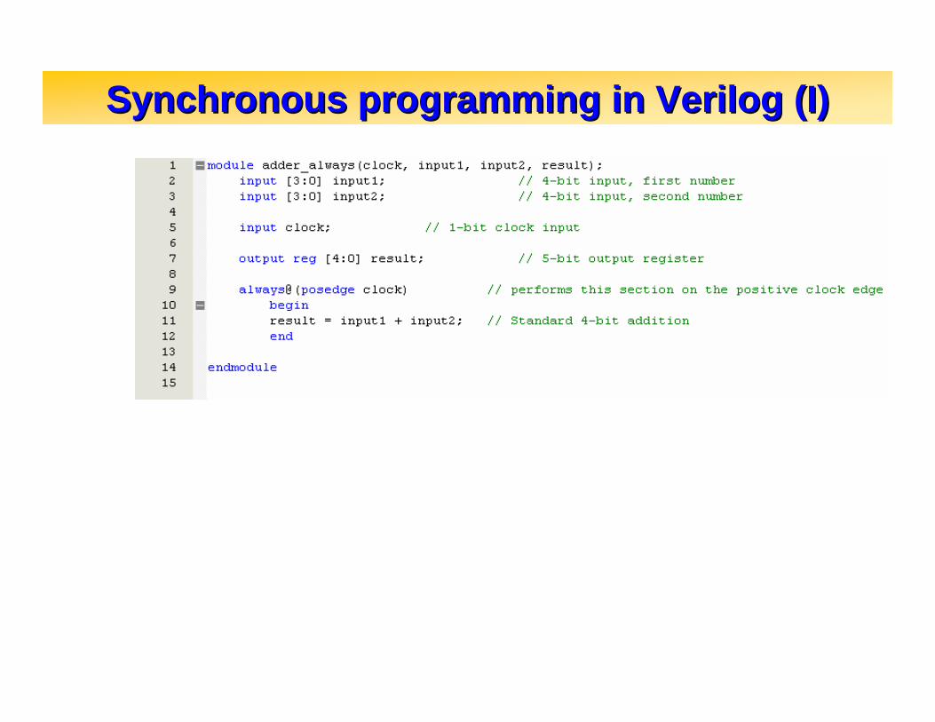
Synchronous programming in Synchronous programming in VerilogVerilog (I)(I)
Synchronous programming in Synchronous programming in VerilogVerilog (I)(I)
Clock Clock variablevariable
output registeroutput register(i.e. flip(i.e. flip--flop memory )flop memory )
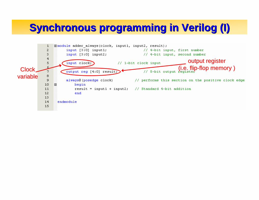
Synchronous programming in Synchronous programming in VerilogVerilog (I)(I)
Clock Clock variablevariable
output registeroutput register(i.e. flip(i.e. flip--flop memory )flop memory )
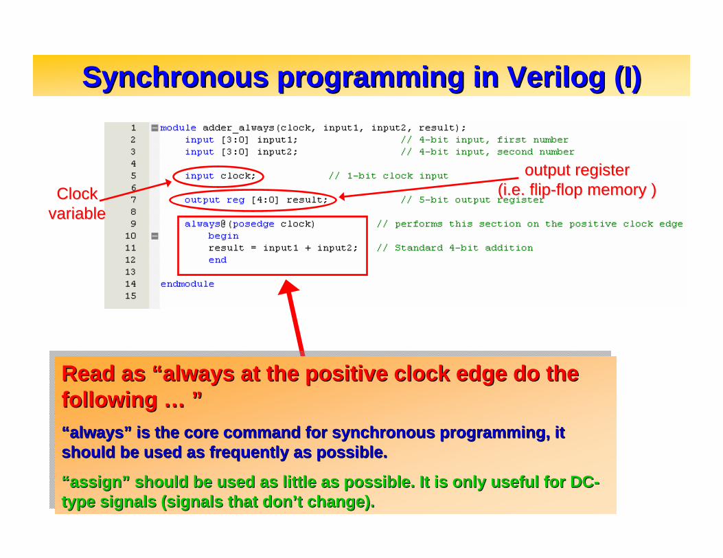
Read as “always at the positive clock edge do the following … ”“always” is the core command for synchronous programming, it should be used as frequently as possible.
“assign” should be used as little as possible. It is only useful for DC-type signals (signals that don’t change).
Read as Read as ““always at the positive clock edge do the always at the positive clock edge do the following following …… ””““alwaysalways”” is the core command for synchronous programming, it is the core command for synchronous programming, it should be used as frequently as possible. should be used as frequently as possible.
““assignassign”” should be used as little as possible. It is only useful for DCshould be used as little as possible. It is only useful for DC--type signals (signals that dontype signals (signals that don’’t change).t change).
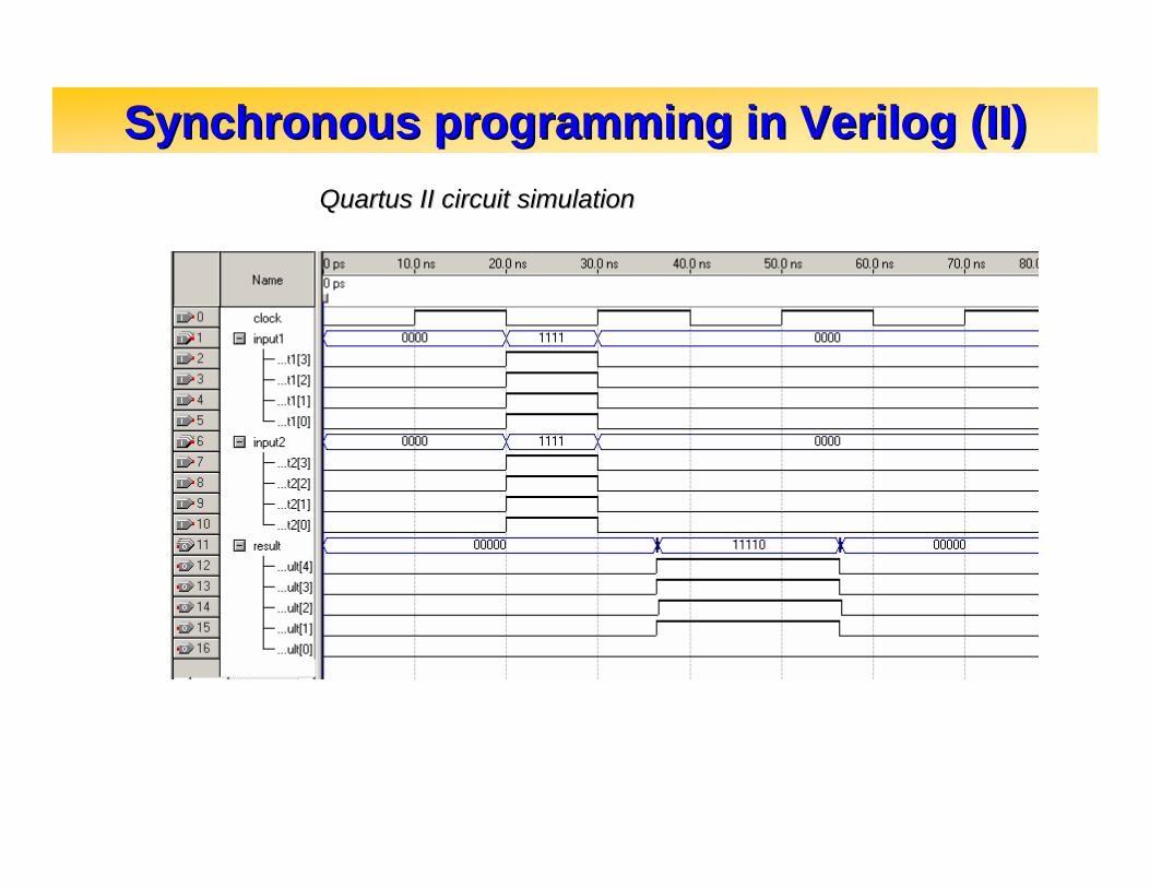
Synchronous programming in Synchronous programming in VerilogVerilog (II)(II)QuartusQuartus II circuit simulationII circuit simulation
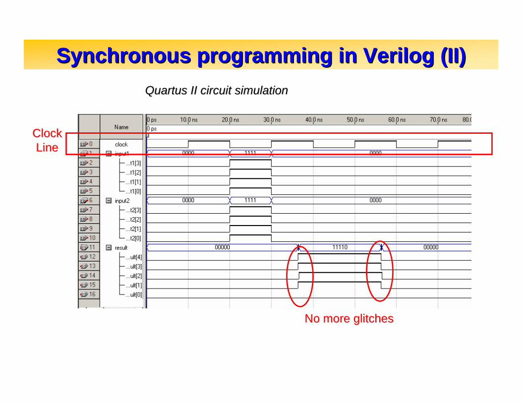
Synchronous programming in Synchronous programming in VerilogVerilog (II)(II)
No more glitchesNo more glitches
ClockClockLineLine
QuartusQuartus II circuit simulationII circuit simulation
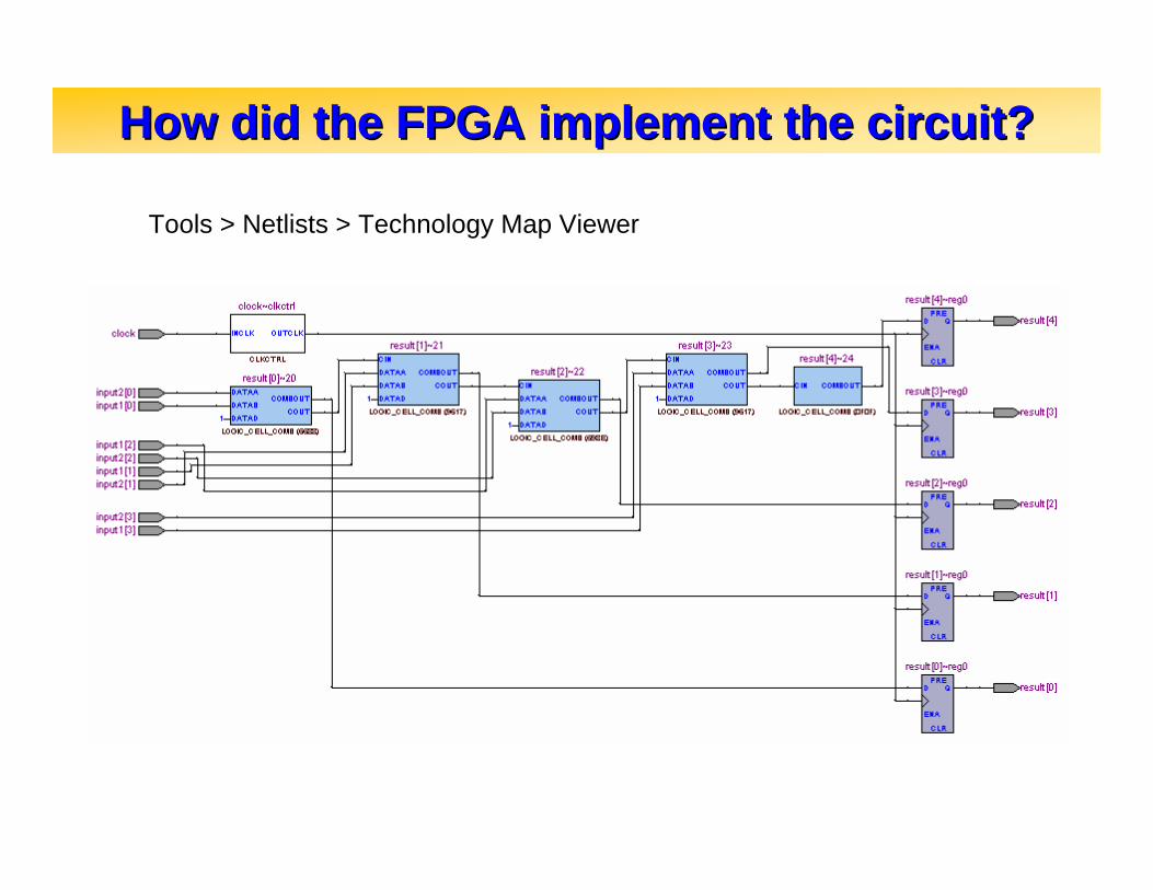
How did the FPGA implement the circuit?How did the FPGA implement the circuit?
Tools > Netlists > Technology Map Viewer
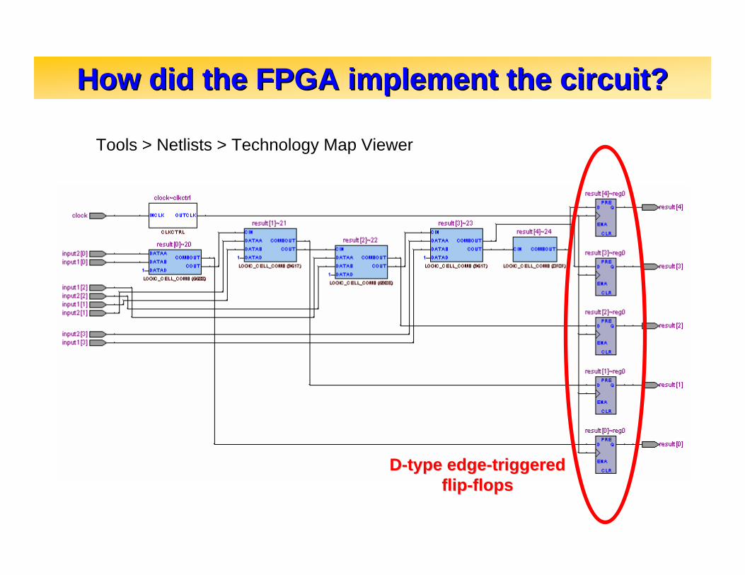
How did the FPGA implement the circuit?How did the FPGA implement the circuit?
Tools > Netlists > Technology Map Viewer
DD--type edgetype edge--triggeredtriggeredflipflip--flopsflops
Always use Always use ““alwaysalways””
A. Stummer, U. of Toronto._
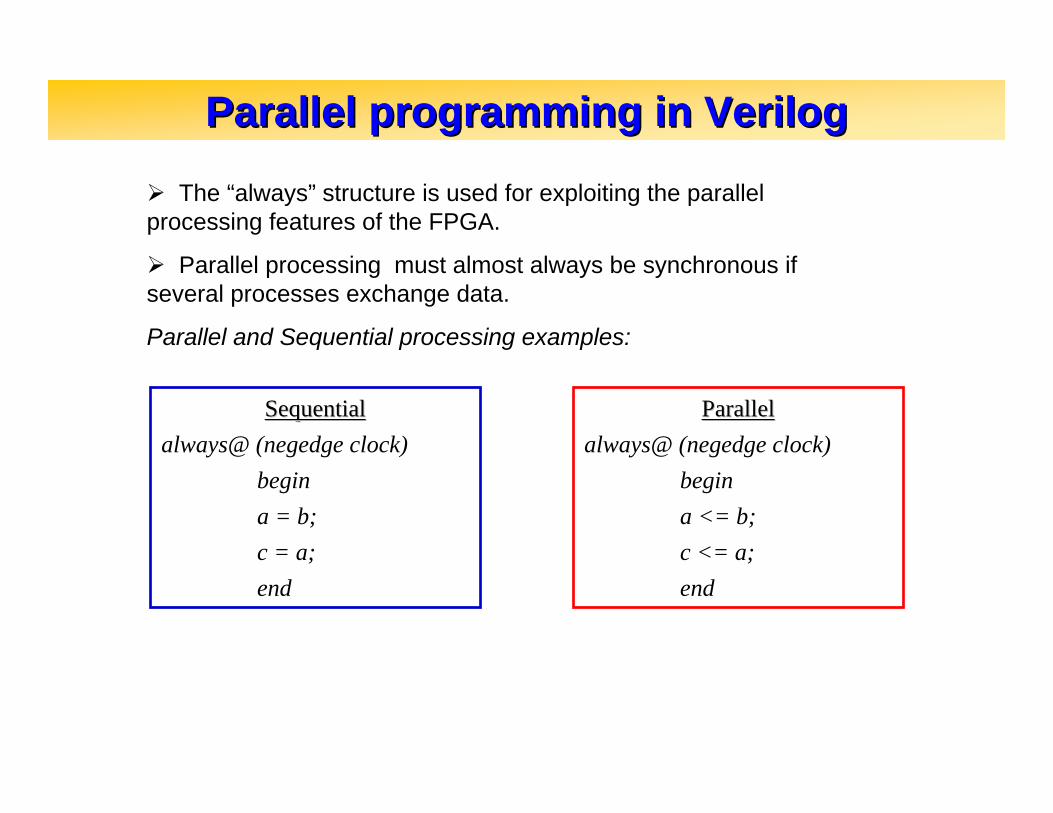
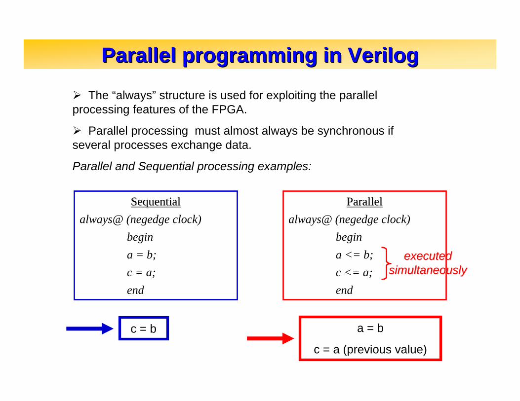
Parallel programming in Parallel programming in VerilogVerilog
The “always” structure is used for exploiting the parallel processing features of the FPGA.
Parallel processing must almost always be synchronous if several processes exchange data.
Parallel and Sequential processing examples:
SequentialSequentialalways@ (negedge clock)
begina = b;c = a;end
ParallelParallelalways@ (negedge clock)
begina <= b;c <= a;end
c = b a = b
c = a (previous value)
executedexecutedsimultaneouslysimultaneously