ELCT201: DIGITAL LOGIC DESIGN - eee.guc.edu.egeee.guc.edu.eg/Courses/Electronics/ELCT201 Digital...
37
ELCT201: DIGITAL LOGIC DESIGN Dr. Eng. Haitham Omran, [email protected] Dr. Eng. Wassim Alexan, [email protected] Lecture 3 ذو الحجة1438 هــWinter 2017 Following the slides of Dr. Ahmed H. Madian
Transcript of ELCT201: DIGITAL LOGIC DESIGN - eee.guc.edu.egeee.guc.edu.eg/Courses/Electronics/ELCT201 Digital...

ELCT201: DIGITAL LOGIC DESIGN Dr. Eng. Haitham Omran, [email protected]
Dr. Eng. Wassim Alexan, [email protected]
Lecture 3
هــ 1438ذو الحجة
Winter 2017
Following the slides of Dr. Ahmed H. Madian

COURSE OUTLINE
1. Introduction
2. Gate-Level Minimization
3. Combinational Logic
4. Synchronous Sequential Logic
5. Registers and Counters
6. Memories and Programmable Logic
2

4-VARIABLE MAP
• Notice the order of the
minterms
• Remember that the cells in the
top row are adjacent to the
cells in the bottom row
• Remember that cells in the most
left column are adjacent to the
cells in the most right column
• Remember that the cells in the
four corners are adjacent to
each
3

NOTES ON A 4-VARIABLE MAP
• The number of adjacent squares that may be combined must always represent a number that is a power of two, such as 1, 2, 4, 8 and 16
• As more adjacent squares are combined, we obtain a product term with fewer literals
• One square represents one minterm, giving a term with 4 literals
• Two adjacent squares represent a term with 3 literals
• Four adjacent squares represent a term with 2 literals
• Eight adjacent squares represent a term with 1 literal
• Sixteen adjacent squares encompass the entire map and produce a function that is always equal to logic 1
4

4-VARIABLE MAP: EXAMPLE I Simplify the Boolean expression:
𝐹 𝐴, 𝐵, 𝐶, 𝐷 = Σ(0,1,2,4,5,7,8,9,10,12,13)
5

4-VARIABLE MAP: EXAMPLE I Simplify the Boolean expression:
𝐹 𝐴, 𝐵, 𝐶, 𝐷 = Σ(0,1,2,4,5,7,8,9,10,12,13)
𝐹 𝐴, 𝐵, 𝐶, 𝐷 = 𝐶′ + 𝐵′𝐷′ + 𝐴′𝐵𝐷
6

4-VARIABLE MAP: EXAMPLE II Simplify the Boolean expression:
𝐹 𝑤, 𝑥, 𝑦, 𝑧 = Σ(0,1,2,4,5,6,8,9,12,13,14)
7

4-VARIABLE MAP: EXAMPLE II Simplify the Boolean expression:
𝐹 𝑤, 𝑥, 𝑦, 𝑧 = Σ(0,1,2,4,5,6,8,9,12,13,14)
𝐹 𝑤, 𝑥, 𝑦, 𝑧 = 𝑦′ +𝑤′𝑧′ + 𝑥𝑧′
8

We can simplify a function by using larger blocks
Do we really need all blocks?
Can we leave some out to further simplify an expression?
Any function needs to contain a special type of blocks
These are called Essential Prime Implicants
We need to define some new terms:
Implicant
Prime implicant
Essential prime implicant
9
CHOICE OF BLOCKS
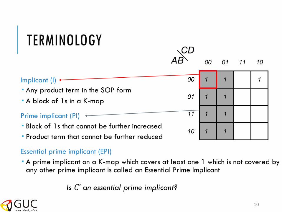
Implicant (I)
Any product term in the SOP form
A block of 1s in a K-map
Prime implicant (PI)
Block of 1s that cannot be further increased
Product term that cannot be further reduced
Essential prime implicant (EPI)
A prime implicant on a K-map which covers at least one 1 which is not covered by any other prime implicant is called an Essential Prime Implicant
10
TERMINOLOGY
Is 𝐶’ an essential prime implicant?

1. Generate all Prime Implicants of the function
2. Include all Essential Prime Implicants
3. For the remaining minterms not included in the Essential Prime Implicants, select a set of other Prime Implicants to cover them, with minimal overlap in the set
4. The resulting simplified function is the logical OR of the product terms selected above
11
THE SYSTEMATIC PROCEDURE FOR SIMPLIFYING BOOLEAN FUNCTIONS

ILLUSTRATING THE TERMS: EXAMPLE I
12
The Prime Implicants are:
• 𝐴′𝐷 𝑔𝑟𝑎𝑦 , • 𝐴𝐶 𝑟𝑜𝑠𝑒 , • 𝐵𝐶′𝐷′ 𝑝𝑖𝑛𝑘 , • 𝐶𝐷 𝑝𝑢𝑟𝑝𝑙𝑒 , • 𝐴𝐵𝐷′ 𝑔𝑟𝑒𝑒𝑛 , • 𝐴′𝐵𝐶′ (𝑦𝑒𝑙𝑙𝑜𝑤).
• Of which only three are Essential:
• 𝐴′𝐷 𝑔𝑟𝑎𝑦 , 𝐴𝐶 𝑟𝑜𝑠𝑒 and 𝐵𝐶′𝐷′ 𝑝𝑖𝑛𝑘 .

ILLUSTRATING THE TERMS: EXAMPLE II
13
The Prime Implicants are:
• 𝐵𝐷 𝑔𝑟𝑎𝑦 , • 𝐴′𝐵𝐶′ 𝑦𝑒𝑙𝑙𝑜𝑤 , • 𝐴𝐶′𝐷 𝑝𝑢𝑟𝑝𝑙𝑒 , • 𝐴𝐵𝐶 𝑔𝑟𝑒𝑒𝑛 , • 𝐴′𝐶𝐷 𝑟𝑜𝑠𝑒 .
• Of which only four are Essential:
𝐴′𝐵𝐶′ 𝑦𝑒𝑙𝑙𝑜𝑤 , 𝐴𝐶′𝐷 𝑝𝑢𝑟𝑝𝑙𝑒 , 𝐴𝐵𝐶 𝑔𝑟𝑒𝑒𝑛 𝑎𝑛𝑑 𝐴′𝐶𝐷 𝑟𝑜𝑠𝑒 .

• Use the SOP simplification on the zeros of the function in the K-map to get 𝐹’
• Find the complement of 𝐹’, i.e. 𝐹’ ′ = 𝐹
• Recall that the complement of a Boolean function can be obtained by (1) taking the dual and (2) complementing each literal
• Or by using DeMorgan’s theorem
14
PRODUCT OF SUMS SIMPLIFICATION USING K-MAPS

15
PRODUCT OF SUMS MINIMIZATION
How to generate a POS from a K-map?
• Use duality of Boolean algebra (DeMorgan’s law)
• Look at the 0s in map instead of the 1s
• Generate blocks around the 0s
This gives the inverse of 𝐹
Use duality to generate POS
Example:
𝐹 = (0,1,2,5,8,9,10)
𝐹′ = 𝐴𝐵 + 𝐶𝐷 + 𝐵𝐷′
𝐹 = (𝐴′ + 𝐵′)(𝐶′ + 𝐷′)(𝐵′ + 𝐷)

GATE IMPLEMENTATION
16

17
EXAMPLE ON POS MINIMIZATION
Given the K-map below, produce the 𝐹′ from the zeros in the map and then obtain 𝐹 from it
𝐹′ = AB′+AC′+A′BCD ′
𝐹 = (AB′)(AC′)(A′BCD′ ) 𝐹 = (𝐴′ + 𝐵)(𝐴′ + 𝐶)(𝐴 + 𝐵′ + 𝐶′ + 𝐷)

18
DON’T CARE CONDITIONS
There may be a combination of input values which: Will never occur,
If they do occur, the output is of no concern
The function value for such combinations is called a don’t care
They are usually denoted with an 𝑋
Each 𝑋 may be arbitrarily assigned the value 0 or 1 in an implementation
Don’t cares can be used to further simplify a function

19
MINIMIZATION USING DON’T CARES
Treat don’t cares as if they are 1s to generate Prime Implicants
Delete Prime Implicants that cover only don’t care minterms
Treat the covering of the remaining don’t care minterms as optional in the selection process (i.e. they maybe, but need not be covered)

𝐹 𝑤, 𝑥, 𝑦, 𝑧 = (1,3,7,11,15) and 𝑑 𝑤, 𝑥, 𝑦, 𝑧 = (0,2,5)
What are the possible solutions?
20
MINIMIZATION EXAMPLE
20

Simplify the function whose K-map is shown at the right
21
EXAMPLE INVOLVING X
𝐹 = 𝐴′𝐶′𝐷 + 𝐴𝐵′ + 𝐶𝐷′ + 𝐴′𝐵𝐶′ or
𝐹 = 𝐴′𝐶′𝐷 + 𝐴𝐵′ + 𝐶𝐷′ + 𝐴′𝐵𝐷′

22
ANOTHER EXAMPLE
Simplify the function whose K-map is shown at the right
𝐹 = 𝐴′𝐶′ + 𝐴𝐵
or
𝐹 = 𝐴′𝐶′ + 𝐵𝐷′

• Digital circuits are frequently constructed with NAND or NOR gates
rather than AND & OR gates.
• NAND and NOR gates are easier to fabricate with electronic components and are the basic gates used in all IC digital logic families
23
NAND AND NOR IMPLEMENTATIONS
A NAND gate has the smallest
propagation time delay among the
other gates, except for the inverter!

NAND AND NOR IMPLEMENTATIONS
• Each NAND or NOR gate requires only 4 transistors
• Each AND gate requires 6 transistors
24

NOT, AND, and OR can be implemented with NAND!
25
LOGIC OPERATION WITH NAND GATE
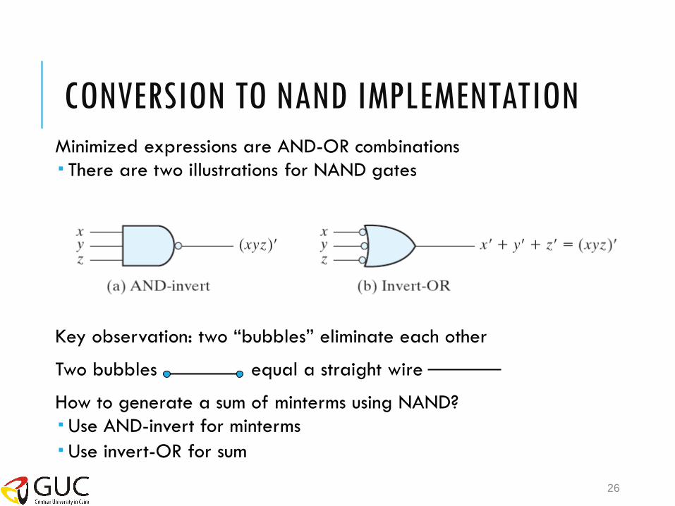
Minimized expressions are AND-OR combinations
There are two illustrations for NAND gates
Key observation: two “bubbles” eliminate each other
Two bubbles equal a straight wire
How to generate a sum of minterms using NAND?
Use AND-invert for minterms
Use invert-OR for sum
26
CONVERSION TO NAND IMPLEMENTATION

• Sum of minterms
• Replace AND with AND-invert and
OR with invert-OR
Still the same circuit!
• Replace AND-invert and invert-OR
with NAND
𝐹 = (𝐴′𝐵′)(𝐶′𝐷′) = 𝐴𝐵 + 𝐶𝐷
27
CONVERSION TO NAND IMPLEMENTATION

Minimize and implement the function
𝐹(𝑥, 𝑦, 𝑧) = (1,2,3,4,5,7),
using only NAND gates
28
NAND EXAMPLE IMPLEMENTATION

Multilevel circuits conversion rules:
1. Convert all AND gates to NAND with AND-invert symbols
2. Convert all OR gates to NAND with invert-OR symbols
3. Check all bubbles in the diagram. For every bubble that is not compensated by another bubble, insert an inverter.
Example:
29
MULTILEVEL NAND CIRCUITS

30
MULTILEVEL NAND CIRCUITS: AN EXAMPLE 𝐹 = (𝐴𝐵′ + 𝐴′𝐵)(𝐶 + 𝐷′)

NOR can also replace NOT, AND & OR
There are two representations of the NOR gate:
31
LOGIC OPERATION WITH NOR GATE

Same rules as for NAND implementations
With NOR
32
CONVERTING TO NOR IMPLEMENTATIONS
𝐹 = (𝐴𝐵′ + 𝐴′𝐵)(𝐶 + 𝐷′)
𝐹 = (𝐴𝐵′ + 𝐴′𝐵)(𝐶 + 𝐷′)

33
DESIGN PROBLEM
Design a digital system whose output is defined as
logically low if the 4-bit input binary number is a
multiple of 3; otherwise, the output will be logically
high. The output is defined if and only if the input
binary number is greater than 2.

34
DESIGN PROBLEM
Design a digital system whose
output is defined as logically
low if the 4-bit input binary
number is a multiple of 3;
otherwise, the output will be
logically high.
The output is defined if and
only if the input binary number
is greater than 2.

35
DESIGN PROBLEM

36
DESIGN PROBLEM
SOP POS
𝑌𝑆𝑂𝑃 = 𝐵′𝐷′ + 𝐴′𝐶′ + 𝐴′𝐵𝐷 + 𝐵𝐶′𝐷 + 𝐴𝐵′𝐶 + 𝐴𝐶𝐷′
𝑌𝑃𝑂𝑆 = (𝐴 + 𝐵)(𝐵 + 𝐶 + 𝐷′)(𝐴 + 𝐶′ + 𝐷)(𝐴′ + 𝐵′ + 𝐶 + 𝐷)(𝐴′ + 𝐵′ + 𝐶′ + 𝐷′)

37
DESIGN PROBLEM
What if you are asked to
implement these digital
circuits using only NAND
gates? Is that possible?