Digital Circuits - Educypedia
54
ENG1030 Electrical Physics and Electronics B.Lovell/T.Downs School of Computer Science and Electrical Engineering 1 28/05/01 Lecture 14 Digital Circuits
Transcript of Digital Circuits - Educypedia

ENG1030 Electrical Physics and Electronics B.Lovell/T.Downs
School of Computer Science and Electrical Engineering
1
28/05/01
Lecture 14
Digital Circuits

ENG1030 Electrical Physics and Electronics B.Lovell/T.Downs
School of Computer Science and Electrical Engineering
2
28/05/01
Lecture 14
Why are we studying digital circuits?
• So that one day you can design something which is better than the ...

ENG1030 Electrical Physics and Electronics B.Lovell/T.Downs
School of Computer Science and Electrical Engineering
3
28/05/01
Lecture 14
Why are we studying digital circuits?
• or something better than the...

ENG1030 Electrical Physics and Electronics B.Lovell/T.Downs
School of Computer Science and Electrical Engineering
4
28/05/01
Lecture 14
Why are we studying digital circuits?
• or even better ....
ENG1030 Electrical Physics and Electronics B.Lovell/T.Downs
School of Computer Science and Electrical Engineering
5
28/05/01
Lecture 14
Why are we studying digital circuits?
• in time, perhaps even....

ENG1030 Electrical Physics and Electronics B.Lovell/T.Downs
School of Computer Science and Electrical Engineering
6
28/05/01
Lecture 14
But .....
We have to start at the beginning....

ENG1030 Electrical Physics and Electronics B.Lovell/T.Downs
School of Computer Science and Electrical Engineering
7
28/05/01
Lecture 14
Number Systems
• Normally we use decimal (base or radix 10)– e.g 123 = (123)10 = 1*102 + 2*101 +3 *100
• For computers it is more convenient to express numbers in binary (base or radix 2)– e.g. (101010)2 = (1*25 + 0*24 + 1*23 + 0*22 +1 *21 + 0*20)
= (32 + 0 + 8 + 0 + 2 + 0) 10= (42) 10
• As binary leads to large strings of 1's and 0's, people often use hexadecimal (base 16) or octal (base 8) to write compact binary numbers

ENG1030 Electrical Physics and Electronics B.Lovell/T.Downs
School of Computer Science and Electrical Engineering
8
28/05/01
Lecture 14
Hexadecimal and Octal
• Conversion to Hex notation– (101010)2 = (0010 1010)2 = 2A (hex)– Group into blocks of 4 and convert each block– 0..9 is same as decimal; also A=10, B=11, C=12,
D=13,E=14,F=15
• Conversion to Octal notation– (101010)2 = (101 010)2 = 52 (octal)– Group into blocks of 3 and convert each block– Only use digits 0..7

ENG1030 Electrical Physics and Electronics B.Lovell/T.Downs
School of Computer Science and Electrical Engineering
9
28/05/01
Lecture 14
Digital Logic and Gates

ENG1030 Electrical Physics and Electronics B.Lovell/T.Downs
School of Computer Science and Electrical Engineering
10
28/05/01
Lecture 14
Analog vs. Digital waveformsAn analog signal assumes a continuous range of values:
A digital signal assumes discrete (isolated, separate) values. Usually there are two permitted values:
t
v(t) ANALOG
t
v(t) DIGITAL

ENG1030 Electrical Physics and Electronics B.Lovell/T.Downs
School of Computer Science and Electrical Engineering
11
28/05/01
Lecture 14
In real life ...A digital signal takes time to change from one value to another, and assumes intermediate values during transition. Steady values are slightly inaccurate. Voltages within certain ranges are guaranteed to be interpreted as certain permitted values (green regions).
t
v(t)
0
Vs
Interpretedas “HIGH”
Interpretedas “LOW”
AMBIGUOUS
(Vs = supply voltage)
A digital signal transition

ENG1030 Electrical Physics and Electronics B.Lovell/T.Downs
School of Computer Science and Electrical Engineering
12
28/05/01
Lecture 14
The digital advantageBecause voltages within a certain range are interpreted as a single value, a digital signal can contain a certain amount of error (e.g. distortion, noise, interference) and still be read correctly. As long as we regenerate the signal (read it and reconstruct it with electronic circuits) before the error becomes too large, we can remove the error.In an analog signal, we cannot tell whether the value is affected by error, because all values are permitted.
Digital signals can be copied, transmitted and processed without error. Analog signals cannot.

ENG1030 Electrical Physics and Electronics B.Lovell/T.Downs
School of Computer Science and Electrical Engineering
13
28/05/01
Lecture 14
Combinational vs. SequentialDigital circuits may be classified as combinational or sequential.In a combinational circuit, the present outputs depend only on present inputs (subject to reaction times).In a sequential circuit, the present outputs may also depend on past outputs and inputs. Sequential circuits usually contain combinationalsubcircuits.The two classes of circuits have different topologies. Sequential circuits contain feedback paths from the outputs to the inputs, while combinational circuits do not.

ENG1030 Electrical Physics and Electronics B.Lovell/T.Downs
School of Computer Science and Electrical Engineering
14
28/05/01
Lecture 14
Asynchronous vs. SynchronousSequential digital circuits may be further classified as asynchronous or synchronous.The outputs of a sequential circuit may be assembled into an ordered list called the state vector, or simply the state.In an asynchronous circuit, the state can change at any time in response to changes in the inputs.In a synchronous circuit, the state can change only at discrete times; these times are determined by a control signal called the clock.We begin by studying combinational circuits ...

ENG1030 Electrical Physics and Electronics B.Lovell/T.Downs
School of Computer Science and Electrical Engineering
15
28/05/01
Lecture 14
Two-valued digital signalsConsider the statement:
THE TELEPHONE LINE IS BUSY.This statement (or “condition”) is either true or false. So we might represent the statement by a digital signal (or “logical variable”) called BUSY, which takes the value TRUE when the line is busy, and the value FALSE when it is not. In other words, the value of BUSY expresses the truth or falsity of the statement represented by BUSY.Note that “BUSY” means the same as “BUSY=TRUE” or “BUSY is TRUE”. The words “is TRUE” are redundant.

ENG1030 Electrical Physics and Electronics B.Lovell/T.Downs
School of Computer Science and Electrical Engineering
16
28/05/01
Lecture 14
Single-variable operation: NOTThe operation NOT (called negation or complementation) is defined as follows: If A is any condition or statement,
“NOT A” means “A=FALSE”.Notice that the definition is a literal interpretation of the word “NOT” : “NOT A” is equivalent to “NOT (A=TRUE)”, so if we take “NOT” literally, we conclude that A=FALSE.Also notice that “NOT A” is just another statement, and is therefore either TRUE or FALSE. When A is TRUE, NOT A is FALSE; when A is FALSE,NOT A is TRUE.

ENG1030 Electrical Physics and Electronics B.Lovell/T.Downs
School of Computer Science and Electrical Engineering
17
28/05/01
Lecture 14
Two-variable operations: OR, ANDWe define the operations OR and AND by taking the words literally.“X OR Y” means “X is true or Y is true”. So “X OR Y” has the value TRUE when either X or Y is TRUE.N.B.: The word OR is interpreted in the inclusive sense. That is, “or” means “and/or”, and “X or Y” means “X or Y or both”.“X AND Y” means “X is true and Y is true”; that is, X AND Y has the value TRUE when both X and Y are TRUE.

ENG1030 Electrical Physics and Electronics B.Lovell/T.Downs
School of Computer Science and Electrical Engineering
18
28/05/01
Lecture 14
Notation; Truth Tables (1)For convenience, we define the following notations:
T = TRUEF = FALSEX’ = X = NOT XXY = X.Y = X AND YX + Y = X OR Y.
Then the operations NOT, OR, AND can be defined using truth tables [right].
A A’
NOT : F TT F
OR ANDA B A+B A B ABF F F F F FF T T F T FT F T T F FT T T T T T

ENG1030 Electrical Physics and Electronics B.Lovell/T.Downs
School of Computer Science and Electrical Engineering
19
28/05/01
Lecture 14
Notation; Truth Tables (2)The values
TRUE and FALSE
may also be called1 and 0,IN and OUT,YES and NO,SET and CLEAR,ON and OFF,MARK and SPACE .
The truth tables have been rewritten using 1 and 0.
X Y’
NOT : 0 11 0
OR ANDX Y X+Y X Y XY0 0 0 0 0 00 1 1 0 1 01 0 1 1 0 01 1 1 1 1 1

ENG1030 Electrical Physics and Electronics B.Lovell/T.Downs
School of Computer Science and Electrical Engineering
20
28/05/01
Lecture 14
Logic gates: OR, AND, NOTIf TRUE and FALSE (or 1 and 0) are represented by two different voltages, we can perform logical operations using circuits called logic gates.An OR gate performs the OR (+) operation. Its circuit symbol is:
An AND gate performs the AND (.) operation. Its circuit symbol is:
A NOT gate or inverterperforms the NOT operation; its circuit symbol is:
XY Z = X+Y
XY Z = XY
X Z = X’

ENG1030 Electrical Physics and Electronics B.Lovell/T.Downs
School of Computer Science and Electrical Engineering
21
28/05/01
Lecture 14
Inversion bubbles, NAND & NOR
The circle in the NOT gate symbol is called an “inversion bubble”. A bubble on the output (or input) of another symbol indicates inversion; e.g.:
means
In fact, an AND gate with output inversion is called a NAND gate (“Not AND”).
Similarly, an OR gate with inverted output is called a NOR gate (“Not OR”).
X Z = X’
XY Z = (XY)’
XY Z = (X+Y)’

ENG1030 Electrical Physics and Electronics B.Lovell/T.Downs
School of Computer Science and Electrical Engineering
22
28/05/01
Lecture 14
NAND and NOR truth tablesBy inverting the output columns of the AND and OR truth tables, we obtain the following:
NOR NANDX Y (X+Y)’ X Y (XY)’0 0 1 0 0 10 1 0 0 1 11 0 0 1 0 11 1 0 1 1 0
For the NOR, the output is false iff (if and only if) either input is true; that is, the output is true iff both inputs are false.For the NAND, the output is false iff both inputs are true; that is, the output is true iff either input is false.In other words ...
ENG1030 Electrical Physics and Electronics B.Lovell/T.Downs
School of Computer Science and Electrical Engineering
23
28/05/01
Lecture 14
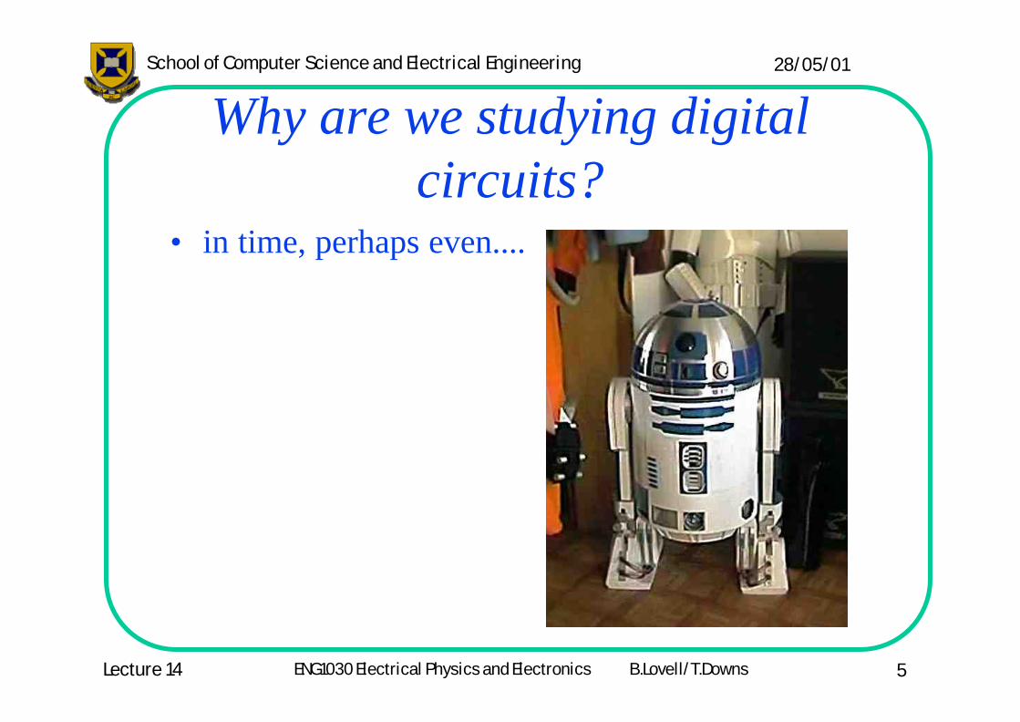
So what is really inside chips?7400 7402
7404 7408
7432

ENG1030 Electrical Physics and Electronics B.Lovell/T.Downs
School of Computer Science and Electrical Engineering
24
28/05/01
Lecture 14
Summary
• Why we study digital circuits?• Analog vs Digital• Combinational and Sequential circuits• Synchronous and Asynchronous circuits• NOT, AND, OR, XOR, NAND, NOR gates

ENG1030 Electrical Physics and Electronics B.Lovell/T.Downs
School of Computer Science and Electrical Engineering
25
28/05/01
Lecture 14
De Morgan’s laws (1)In a NOR gate, the output is TRUEiff the inverses of both inputs are TRUE; that is, a NOR gate performs and AND operation on the inverses. So there are two symbols for a NOR gate:
In a NAND gate, the output is TRUE iff the inverse of either input is TRUE; that is, a NAND gate does an OR operation on the inverses. So there are two symbols for a NAND gate:

ENG1030 Electrical Physics and Electronics B.Lovell/T.Downs
School of Computer Science and Electrical Engineering
26
28/05/01
Lecture 14
De Morgan’s laws (2)If we convert the two NOR symbols into algebraic expressions and equate them, we get
(X+Y)’ = X’ Y’ .Doing likewise with the NAND symbols, we get
(XY)’ = X’+Y’ .These equations are called De Morgan’s laws. If they are not already obvious, try expressing them in words:
Not (X or Y) = neither X nor Y = (not X) and (not Y).Not (X and Y) = not both X and Y = (not X) or (not Y).
Now omit the middle expressions.

ENG1030 Electrical Physics and Electronics B.Lovell/T.Downs
School of Computer Science and Electrical Engineering
27
28/05/01
Lecture 14
Positive and negative logic (1)Suppose we represent logical variables using two voltages called HIGHand LOW; HIGH is the higher voltage.Suppose we have a circuit with two inputs and one output, in which the output is HIGH iff both inputs are HIGH. If HIGH means 1 and LOW means 0 (“positive logic”), this device is an AND gate.The same circuit may be described equally well by saying that the output is LOW iff at least one input is LOW. So if LOW means 1 and HIGH means 0 (“negative logic”) the same device is an OR gate.

ENG1030 Electrical Physics and Electronics B.Lovell/T.Downs
School of Computer Science and Electrical Engineering
28
28/05/01
Lecture 14
Positive and negative logic (2)Consider another circuit with two inputs and one output, in which the output is HIGH iff at least one input is HIGH. In positive logic, this device is an OR gate.We can describe the same circuit by saying that the output is LOW iff both inputs are LOW. So in negative logic, the same device is an AND gate.In positive or negative logic, an inverter still inverts.In summary, switching from positive logic to negative logic (or back) changes ORs to ANDs and ANDs to ORs. This fact is known as the duality principle.

ENG1030 Electrical Physics and Electronics B.Lovell/T.Downs
School of Computer Science and Electrical Engineering
29
28/05/01
Lecture 14
Two theorems for the price of one!Suppose two logical expressions are known to be identical (i.e. equal for all values of the variables). We implement both expressions as electronic circuits, using positive logic. By the duality principle, if we modify the two expressions by replacing all ORs in the expressions with ANDs, ANDswith ORs, 1’s with 0’s, and 0’s with 1’s, we get the expressions implemented by the same circuits in negative logic; these expressions are also identical.The second identity is called the dual of the first identity; the dual is obtained by interchanging ANDs and ORs, and 1’s and 0’s.

ENG1030 Electrical Physics and Electronics B.Lovell/T.Downs
School of Computer Science and Electrical Engineering
30
28/05/01
Lecture 14
Duality and De Morgan’s laws (1)Recall that De Morgan’s laws are
(X+Y)’ = X’ Y’ and (XY)’ = X’+Y’ .First notice that each of these laws is the dual of the other.The gate symbols introduced so far assume positive logic. A negative-logic gate is indicated by drawing triangles on the inputs and outputs, e.g.
Negative-logic AND gate; Negative-logic OR gate.

ENG1030 Electrical Physics and Electronics B.Lovell/T.Downs
School of Computer Science and Electrical Engineering
31
28/05/01
Lecture 14
Duality and De Morgan’s laws (2)One way to make a positive-logic OR gate is to place inverters on the inputs and output of a negative-logic OR gate.
The inverters convert to negative logic before the OR, then back to positive.
By duality, the negative-logic OR gate is a positive-logic AND gate. So we have:
Since this is an OR gate,X+Y = (X’ Y’)’.
Inverting both sides gives the first De Morgan law:
(X+Y)’ = X’ Y’.

ENG1030 Electrical Physics and Electronics B.Lovell/T.Downs
School of Computer Science and Electrical Engineering
32
28/05/01
Lecture 14
Duality and De Morgan’s laws (3)Similarly, a positive-logic AND gate can be made like this:
By duality, this is equivalent to
Since this is an AND gate, we have
XY = (X’+Y’)’.Inverting both sides gives the second De Morgan law:
(XY)’ = X’+Y’.Thus De Morgan’s laws are related by duality, and are consequences of duality.

ENG1030 Electrical Physics and Electronics B.Lovell/T.Downs
School of Computer Science and Electrical Engineering
33
28/05/01
Lecture 14
The Exclusive-OR (XOR) operationThe OR function in logic is inclusive; “X or Y” means “X or Y or both”. The exclusive-OR function, as its name suggests, excludes the “or both” option: “X xor Y” means “X or Y but not both”. In equations, X xor Y is often written
X Y.
The truth table isX Y X xor Y0 0 00 1 11 0 11 1 0
and the gate symbol isX
YX xor Y
ENG1030 Electrical Physics and Electronics B.Lovell/T.Downs
School of Computer Science and Electrical Engineering
34
28/05/01
Lecture 14
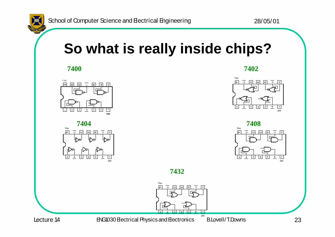
Exclusive-NOR/equivalence gateInverting the output of an XOR gate gives an exclusive-NOR (XNOR) or equivalence gate.XNOR truth table:
X Y (X xor Y)’0 0 10 1 01 0 01 1 1
XNOR gate symbol:
The truth table shows why the XNOR gate is called an equivalence gate: the output is true iff the inputs are the same. (For the XOR, the output is true iffthe inputs are different.)
X
Y(X xor Y)’

ENG1030 Electrical Physics and Electronics B.Lovell/T.Downs
School of Computer Science and Electrical Engineering
35
28/05/01
Lecture 14
AND-OR formulation of XORAs we shall see, XOR gates are used in addition and subtraction circuits. Hence it is of interest to see how such gates can be constructed. From the truth table, X xor Y is true iff (X is false and Y is true) or (X is true and Y is false).
More concisely, “X xor Y” means “([not X] and Y) or (X and [not Y])”. That is
X xor Y = X’Y + XY’.Note the priority of operators in the above equation: NOT (’) comes first, followed by AND, then OR. (Cf. powers, multiplication, addition.)

ENG1030 Electrical Physics and Electronics B.Lovell/T.Downs
School of Computer Science and Electrical Engineering
36
28/05/01
Lecture 14
AND-OR and NAND-NAND formsThe function
X xor Y = X’Y + XY’may be implemented using the circuit below.
Now let us introduce two inversion pairs [top right].
This circuit is equivalent to the previous one [left] because the inversions cancel out. But now all the multiple-input gates are NAND gates.
X
Y
X xor Y
X
Y
X xor Y
X’Y
XY’

ENG1030 Electrical Physics and Electronics B.Lovell/T.Downs
School of Computer Science and Electrical Engineering
37
28/05/01
Lecture 14
Advantage of NAND-NAND form (1)In the most widely used IC technologies (e.g. CMOS, NMOS, TTL), a NAND gate requires less silicon area than an AND or OR gate. CMOS circuits for an invertor and a positive-logic NAND gate are shown below.
X X’
VDD
VDD
X
Y
XY’p-channel
n-channel
(All transistors are enhancement-mode.)
NOT: NAND:
ENG1030 Electrical Physics and Electronics B.Lovell/T.Downs
School of Computer Science and Electrical Engineering
38
28/05/01
Lecture 14
Advantage of NAND-NAND form (2)In most IC technologies, it is easier to make a gate with inversion than without, because the common-emitter or common-source transistor configuration gives an inversion.In CMOS, an AND gate requires a NAND gate followed by an inverter. A NOR gate is just as simple as a NAND, while an OR requires a NORfollowed by an inverter.Exercise: Sketch a circuit for a CMOS NOR gate in positive logic. (Hint: What does the NAND circuit [previous slide] become if we use negative logic? See the following slide for some useful information on MOS transistors.)

ENG1030 Electrical Physics and Electronics B.Lovell/T.Downs
School of Computer Science and Electrical Engineering
39
28/05/01
Lecture 14
Enhancement-mode MOS transistorsAn enhancement-mode MOSFET (Metal-Oxide-Semiconductor Field-Effect Transistor) may be n-channel or p-channel:
For digital purposes, an MOSFET is a switch between the source and drain. For the n-channel enhancement-mode MOSFET, the switch is closed (on) if the gate voltage is substantially more positive than both the source and drain voltages; it is open (off) if the gate voltage is not substantially more positive than at least one of the source and drain voltages. Intermediate gate voltages are not used. For the p-channel, write “negative” instead of “positive”.
p-channeln-channel
Source
DrainGate
Drain
SourceGate

ENG1030 Electrical Physics and Electronics B.Lovell/T.Downs
School of Computer Science and Electrical Engineering
40
28/05/01
Lecture 14
NAND-NAND & De Morgan’s lawsRecall that
X xor Y = X’Y + XY’.
The first De Morgan law is(A+B)’ = A’B’.
Inverting both sides givesA+B = (A’B’)’.
Applying this to the OR in the top equation gives the NAND-NAND form:
X xor Y = [(X’Y)’ (XY’)’]’.
The two De Morgan laws and their inverted forms are contained in the ruleTo make an x-gate, invert
the inputs to a y-gate,where one of x,y is an AND and the other is an OR, and only one is inverted. There are four combinations. List them!

ENG1030 Electrical Physics and Electronics B.Lovell/T.Downs
School of Computer Science and Electrical Engineering
41
28/05/01
Lecture 14
Don’t forget truth tables!In the preceding slides, De Morgan’s laws and the AND-OR formulation of the XOR function have been derived by translating verbal statements into logical equations. This has been done to emphasise the connection between digital logic (AND/OR/NOT) and everyday logic (“and”, “or”, “not”).But all the equations can be verified by constructing the truth tables for the left-hand and right-hand sides, and observing that the truth tables are the same. Sometimes this is the most convenient method of proof.

ENG1030 Electrical Physics and Electronics B.Lovell/T.Downs
School of Computer Science and Electrical Engineering
42
28/05/01
Lecture 14
Commutative lawsThe OR, AND and XOR functions are commutative; that is, for all X,Y,
X+Y = Y+XXY = YX
X xor Y = Y xor X.These laws are obvious because the verbal definitions of OR, AND and XOR use words like
“either”, “both” and “only one”, which do not distinguish between the two inputs.The laws can be verified by swapping the input columns in the truth tables, and then reordering the rows to restore the original patterns of 1’s and 0’s. Try it.

ENG1030 Electrical Physics and Electronics B.Lovell/T.Downs
School of Computer Science and Electrical Engineering
43
28/05/01
Lecture 14
Associative lawsOR and AND are also associative; that is, for all X,Y,Z,
(X+Y)+Z = X+(Y+Z)(XY)Z = X(YZ).
These laws can also be verified using truth tables.The implication is that the expressions X+Y+Z and XYZ are unambiguous.
Repeated applications of the associative laws indicate that OR and AND combinations with 4 or more variables are also unambiguous.The commutative law can be brought in to show that these multi-variable expressions can be written in any order.

ENG1030 Electrical Physics and Electronics B.Lovell/T.Downs
School of Computer Science and Electrical Engineering
44
28/05/01
Lecture 14
Many-input gatesExpressions with three or more variables are implemented by logic gates with three or more inputs:
Their names and functions of these gates are obvious. Of course the outputs may be inverted [top right].
In a multi-input AND gate, the output is true iff all of the inputs are true. In a multi-input OR gate, the output is true iff any (one or more) of the inputs are true. In multi-input NAND and NOR gates, the output is FALSE under the same input conditions.

ENG1030 Electrical Physics and Electronics B.Lovell/T.Downs
School of Computer Science and Electrical Engineering
45
28/05/01
Lecture 14
De Morgan’s laws - many inputs (1)The verbal “proofs” of De Morgan’s laws [slides 14-16] can be modified for more than two inputs by writing “all” instead of “both”, and “any” or “one or more” instead of “either”. (The same trick extends the verbal definitions of AND and OR to several inputs [previous slide].)For a more rigorous proof, we can show algebraically that the three-input forms follow from the two-input forms:
(X+Y+Z)’ = ((X+Y)+Z)’ = (X+Y)’Z’ = (X’Y’)Z’ = X’Y’Z’.
... and similarly for the other law. In the same way, the laws for n+1 variables follow from those for n variables.

ENG1030 Electrical Physics and Electronics B.Lovell/T.Downs
School of Computer Science and Electrical Engineering
46
28/05/01
Lecture 14
De Morgan’s laws - many inputs (2)The many-input forms of De Morgan’s laws, like the two input forms, yieldalternative symbols for logic gates:
NAND:
NOR:
The summary rule still holds: To make an x-gate, invert the inputs to a y-gate, where one of x,y is an AND and the other is an OR, and only one is inverted.

ENG1030 Electrical Physics and Electronics B.Lovell/T.Downs
School of Computer Science and Electrical Engineering
47
28/05/01
Lecture 14
Other associative laws? (1)Recall that the associative laws hold for OR and AND. They do not hold for NOR or NAND. ((X+Y)’+Z)’ is not identical to (X+(Y+Z)’)’, and neither is identical to the three-input NOR function
(X+Y+Z)’ = ((X+Y)+Z)’ = (X+(Y+Z))’.Similarly, ((XY)’Z)’ is not identical to (X(YZ)’)’, and neither is identical to the three-input NAND function
(XYZ)’ = ((XY)Z)’ = (X(YZ))’.The three-way equalities are of course based on the associative laws for OR and AND.

ENG1030 Electrical Physics and Electronics B.Lovell/T.Downs
School of Computer Science and Electrical Engineering
48
28/05/01
Lecture 14
Other associative laws? (2)The associative laws do hold for XOR and XNOR.In fact, cascaded XOR or XNOR gates can be used as parity testers. If we combine n inputs in arbitrary order using n-1 XOR gates, the output is TRUE (1) iff the number of TRUE inputs is odd. If we do the same thing with XNOR (equivalence) gates, the output is FALSE (0) iff the number of FALSE inputs is odd. (The symmetry between these statements reflects the fact that XNOR is the dual of XOR; that is, an XOR gate in positive logic is an XNOR in negative logic, and vice versa.)

ENG1030 Electrical Physics and Electronics B.Lovell/T.Downs
School of Computer Science and Electrical Engineering
49
28/05/01
Lecture 14
Parity-testing circuitsEach of the following circuits combines n inputs using n-1 XOR gates, and produces an output of 1 iff the number of input 1’s is odd. Other gate arrangements are possible.
n = 3:
n = 6:

ENG1030 Electrical Physics and Electronics B.Lovell/T.Downs
School of Computer Science and Electrical Engineering
50
28/05/01
Lecture 14
Proof of parity-testing property (1)Proof for XOR gates: Suppose we combine n inputs in arbitrary order using n-1 XOR gates. Any combination of inputs can be set up by first setting all inputs to 0, then toggling the inputs that are required to be 1. When the n inputs are 0, all the inputs and outputs of all the gates are 0, and the final output is 0. If we toggle an input, this toggles the output of the gate to which the input is connected. If that output is fed into another gate, its output also toggles, and so on. So the final output is toggled for every input that is set to 1. If the number of 1’s (and toggles) is odd, the output ends up being 1.

ENG1030 Electrical Physics and Electronics B.Lovell/T.Downs
School of Computer Science and Electrical Engineering
51
28/05/01
Lecture 14
Proof of parity-testing property (2)Proof for XNOR gates: This is the same as the proof for XOR gates, except that we start with all the inputs and outputs of all the gates set to 1, and toggle the inputs that are required to be 0.Alternatively, we can suppose that the XOR array is implemented in positive logic, and switch to negative logic. Then the 0’s become 1’s, the 1’s become 0’s, the XORs become XNORs, and the XOR property [proven on the previous slide] turns into the XNOR property.It remains to prove that XNOR is the dual of XOR ...
ENG1030 Electrical Physics and Electronics B.Lovell/T.Downs
School of Computer Science and Electrical Engineering
52
28/05/01
Lecture 14
Proof of XOR/XNOR dualityAn XOR gate gives an output of 1 iff the inputs are different. An XNOR gives an output of 1 iff the inputs are the same. For a given circuit, switching from positive to negative logic does not change the sameness ordifferentness of the inputs, but it does invert the meaning of the output; the inversion changes XOR to XNOR and vice versa.

ENG1030 Electrical Physics and Electronics B.Lovell/T.Downs
School of Computer Science and Electrical Engineering
53
28/05/01
Lecture 14
Proof of XOR/XNOR associative lawWe have proven that the function performed by a cascade of XOR (or XNOR) gates can be described in terms of the parity of the number of 1’s (or 0’s) among the inputs. This description says nothing about the order in which the inputs and intermediate outputs are combined in pairs. So all such combinations must produce the same result; that is, the associative law must hold.
XOR parity testers are used in addition circuits (as we shall see) and in the detection of transmission errors.

ENG1030 Electrical Physics and Electronics B.Lovell/T.Downs
School of Computer Science and Electrical Engineering
54
28/05/01
Lecture 14


![[ 3 ] Power MOSFET in Detail - Educypedia](https://static.fdocuments.us/doc/165x107/613d0efc736caf36b758d244/-3-power-mosfet-in-detail-educypedia.jpg)