Digital Circuits
104
Introduction to Digital Concepts Section 1.1 Numerical Presentation In science, technology, business, and, in fact, most other fields of endeavor, we are constantly dealing with quantities. Quantities are measured, monitored, recorded, manipulated arithmetically, observed, or in some other way utilized in most physical systems. It is important when dealing with various quantities that we be able to represent their values efficiently and accurately. There are basically two ways of representing the numerical value of quantities: analog and digital. Analog Representation Analog Representation Analog Representation Analog Representation In analog representation a quantity is represented by a voltage, current, or meter movement that is proportional to the value of that quantity. Analog quantities such as those cited above have an important characteristic: they can vary over a continuous range of values. Below is a diagram of analog voltage vs time: C H A P T E R + + + + 1-1 Numerical Representations 1-2 Advantages and Limitations of Digital Techniques 1-3 Digital Number Systems 1-4 Representing Binary Quantities + + + + 1
description
If you like this document and you want to thank me please register here: http://www.income-web.biz?a_aid=4bd59700c7413 This is not a scam. I just want to earn money through online ads. Just click the link and register there IF you want to help me back. Thanks.
Transcript of Digital Circuits

Introduction to
Digital Concepts
Section 1.1 Numerical Presentation
In science, technology, business, and, in fact, most other fields of endeavor, we are constantly dealing with quantities. Quantities are measured, monitored, recorded, manipulated arithmetically, observed, or in some other way utilized in most physical systems. It is important when dealing with various quantities that we be able to represent their values efficiently and accurately. There are basically two ways of representing the numerical value of quantities: analog and digital.
Analog RepresentationAnalog RepresentationAnalog RepresentationAnalog Representation
In analog representation a quantity is represented by a voltage, current, or meter movement that is proportional to the value of that quantity. Analog quantities such as those cited above have an important characteristic: they can vary over a continuous range of values. Below is a diagram of analog voltage vs time:
C H A P T E R
+ + + +
1-1 Numerical Representations
1-2 Advantages and Limitations of Digital Techniques
1-3 Digital Number Systems
1-4 Representing Binary Quantities
+ + + +
1111

Chapter 1 Introduction to Digital Concepts 2
Building skills for success
Digital RepresentaDigital RepresentaDigital RepresentaDigital Representationtiontiontion
In digital representation the quantities are represented not by proportional quantities but by symbols called digits. As an example, consider the digital watch, which provides the time of day in the form of decimal digits which represent hours and minutes (and sometimes seconds). As we know, the time of day changes continuously, but the digital watch reading does not change continuously; rather, it changes in steps of one per minute (or per second). In other words, this digital representation of the time of day changes in discrete steps, as compared with the representation of time provided by an analog watch, where the dial reading changes continuously. Below is a diagram of digital voltage vs time:
The major difference between analog and digital quantities, then, can be simply stated as follows:
Analog = continuous Digital = discrete (step by step)

Chapter 1 Introduction to Digital Concepts 3
Building skills for success
FIGURE 1-1 Analog versus digital: (a) analog waveform; (b) digital waveform; (c) analog watch; (d) digital watch.
Section 1.2 Advantages and Limitations of Digital Techniques
AdvantagesAdvantagesAdvantagesAdvantages
1. Easier to design. Exact values of voltage or current are not important, only the range (HIGH or LOW) in which they fall.
2. Information storage is easy. 3. Accuracy and precision are greater. 4. Operation can be programmed. Analog systems can also be programmed, but the variety and
complexity of the available operations is severely limited. 5. Digital circuits are less affected by noise. As long as the noise is not large enough to prevent
us from distinguishing a HIGH from a LOW. 6. More digital circuitry can be fabricated on IC chips.

Chapter 1 Introduction to Digital Concepts 4
Building skills for success
LimitationsLimitationsLimitationsLimitations
There is really only one major drawback when using digital techniques:
The real world is mainly analog. Most physical quantities are analog in nature, and it is these quantities that are often the inputs and outputs that are being monitored, operated on, and controlled by a system. To take advantage of digital techniques when dealing with analog inputs and outputs, three steps must be followed:
1. Convert the real-world analog inputs to digital form. (ADC) 2. Process (operate on) the digital information. 3. Convert the digital outputs back to real-world analog form. (DAC)
The following diagram shows a temperature control system that requires analog/digital conversions in order to allow the use of digital processing techniques.

Chapter 1 Introduction to Digital Concepts 5
Building skills for success
FIGURE 1-2 The process of converting analog sound to digital and then back to analog.
Section 1.3 Number Systems
Many number systems are in use in digital technology. The most common are the decimal, binary, octal, and hexadecimal systems. The decimal system is clearly the most familiar to us because it is a tool that we use every day. Examining some of its characteristics will help us to better understand the other systems.
Decimal Number SystemDecimal Number SystemDecimal Number SystemDecimal Number System
Decimal System The decimal system is composed of 10 numerals or symbols. These 10 symbols are 0, 1, 2, 3, 4, 5, 6, 7, 8, 9; using these symbols as digits of a number, we can express any quantity. The decimal system, also called the base-10 system because it has 10 digits. It has a radix or a base of 10.
103 10
2 10
1 10
0 10
-1 10
-2 10
-3
=1000 =100 =10 =1 . =0.1 =0.01 =0.001
Most Significant Digit
Decimal point
Least Significant Digit

Chapter 1 Introduction to Digital Concepts 6
Building skills for success
Ex. 17610 = find its positional notation
= 1 X 10² + 7 X 101 + 6 X 10
0
= 100 + 70 + 6 = 17610
Binary Number SystemBinary Number SystemBinary Number SystemBinary Number System
In the binary system, there are only two symbols or possible digit values, 0 and 1. This base-2 system can be used to represent any quantity that can be represented in decimal or other number system. It has a radix or a base of 2.
23 2
2 2
1 2
0 2
-1 2
-2 2
-3
=8 =4 =2 =1 . =1/2 =1/4 =1/8
Most Significant Bit
Binary point
Least Significant Bit
Ex.1. 110112 = 1 X 2
4 + 1 X 2
3 + 0 X 2
2 + 1 X 2
1 + 1 X 2
0
= 16 + 8 + 0 +2 +1 = 2710
10.11102 = 1 X 21 + 0 X 2
0 + 1 X 2
-1 + 1 X 2
-2 + 1 X 2
-3 + 0 X 2
-4
= 2 + 0 + 0.5 + 0.25 + 0.125 = 2.87510

Chapter 1 Introduction to Digital Concepts 7
Building skills for success
Binary CountingBinary CountingBinary CountingBinary Counting
The Binary counting sequence is shown in the table
Octal Number SystemOctal Number SystemOctal Number SystemOctal Number System
A number system with 8 separate symbols represented by 0, 1, 2, 3, . . . 7. It has a radix or base of 8. Ex.1. 176.58 = 1 X 8
2 + 7 X 8
1 + 6 X 8
0 + 5 X 8
-1
= 64 + 56 + 6 + 0.625 = 126.62510
Hexadecimal Number SystemHexadecimal Number SystemHexadecimal Number SystemHexadecimal Number System
A number system with 16 separate symbols represented by 0, 1, 2, 3, …9, A, B, C, D, E, F. It has a radix or a base of 16. Ex.1. 10B.CF16 = 1 X 16
2 + 0 X 16
1 + 11 X 16
0 + 12 X 16
-1 + 15 X 16
-2
= 256 + 0 + 11 + 0.75 + 0.0586 = 267.808610
Chapter 1 Introduction to Digital Concepts 8
Building skills for success
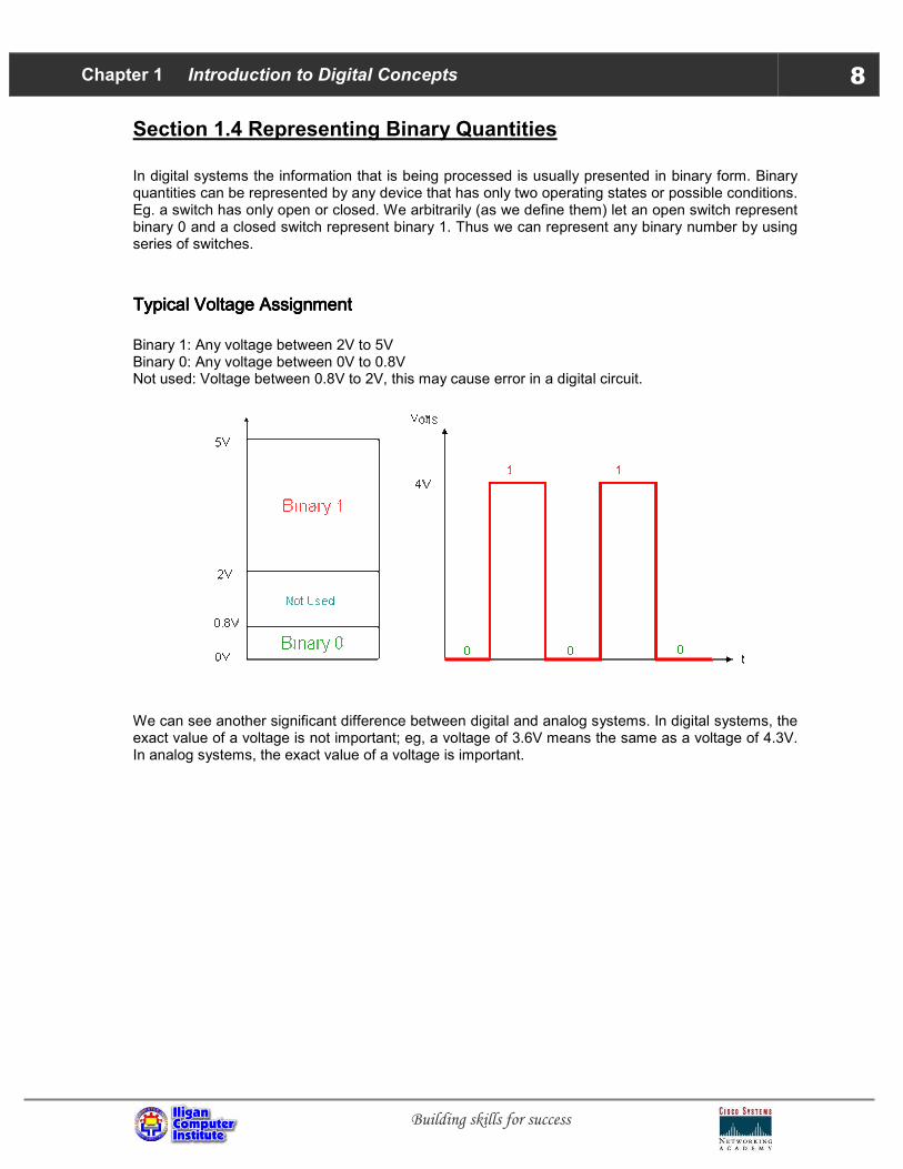
Section 1.4 Representing Binary Quantities
In digital systems the information that is being processed is usually presented in binary form. Binary quantities can be represented by any device that has only two operating states or possible conditions. Eg. a switch has only open or closed. We arbitrarily (as we define them) let an open switch represent binary 0 and a closed switch represent binary 1. Thus we can represent any binary number by using series of switches.
TypiTypiTypiTypical Voltage Assignmentcal Voltage Assignmentcal Voltage Assignmentcal Voltage Assignment
Binary 1: Any voltage between 2V to 5V Binary 0: Any voltage between 0V to 0.8V Not used: Voltage between 0.8V to 2V, this may cause error in a digital circuit.
We can see another significant difference between digital and analog systems. In digital systems, the exact value of a voltage is not important; eg, a voltage of 3.6V means the same as a voltage of 4.3V. In analog systems, the exact value of a voltage is important.

Chapter 1 Introduction to Digital Concepts 9
Building skills for success
Chapter 1Chapter 1Chapter 1Chapter 1 Self TestSelf TestSelf TestSelf Test
Choose the correct answers in the following questions.
1. What is the difference between digital and analog techniques?
Digital quantities can take on any value over a continuous range.
Digital quantities can take on discrete value over a range.
Actually, they are indifferent, only digital is a new technology inveneted in 1980s.
None of the above. 2. Which involves digital quantities:
Ten-Position switch.
Current meter
Temperature.
Radio volume control in 80s. 3. Which following is not an advantage of digital technique?
Digital system is easier to design.
Accuracy and precision are greater.
Digital circuits are less affected by noise
Digital quantities are equivalent to real-world physical quantities. 4. What is the largest decimal number that can be represented using 8 bits?
128
255.
256
1024. 5. Which of the following range is the not used in voltage assignment in digital system:
0.4V - 1.2V
0.8V - 2V
0.8V - 2.4V
1V - 2.4V

Number System and
Codes
The binary number system is the most important one in digital systems,
but several others are also important. The decimal system is important because it is universial used to represent quantites outside a digital system. This means that there will be situations where decimal values have to be converted to binary values before they are entered into the digital system. In additional to binary ans decimal, two other number systems find wide-spread applications in digital systems. The octal (base-8) and hexadecimal (base-16) number systems are both used for the same purpose- to provide an efficient means for representing large binary system. This chapter will show you how to perform these conversions.
C H A P T E R
+ + + +
2-1 Binary-to-Decimal Conversion
2-2 Decimal-to-Binary Conversion
2-3 Octal Number System
2-4 Hexadecimal Number System
+ + + +
2222

Chapter 2 Number System and Codes 11
Building skills for success
Section 2.1 Binary-To-Decimal Conversion
Any binary number can be converted to its decimal equivalent simply by summing together the weights of the various positions in the binary number which contain a 1.
1 1 0 1 1 2 (binary)
24+23+0+21+20 = 16+8+0+2+1
= 2710 (decimal)
And by positional notation
1 0 1 1 0 1 0 1 2 (binary)
27+0+25+24+0+22+0+20 = 128+0+32+16+0+4+0+1
= 18110 (decimal)
You should noticed the method is find the weights (i.e., powers of 2) for each bit position that contains a 1, and then to add them up.
Section 2.2 Decimal Number System
There are 2 methods:
(A) Repeated Division (Long method)
45 10 = 32 + 0 + 8 + 4 +0 + 1
= 25+0+23+22+0+20
= 1 0 1 1 0 12

Chapter 2 Number System and Codes 12
Building skills for success
The Flow chart for repeated-division method is as follow:
More Examples:
Decimal to Binary
2110 � convert to base 2
Answer: 2110 = 101012

Chapter 2 Number System and Codes 13
Building skills for success
Decimal to Octal
2110 � convert to base 8
Answer: 2110 = 258
Decimal to Hexadecimal
2110 � convert to base 16
Answer: 2110 = 1516
(B) Revese of Binary(B) Revese of Binary(B) Revese of Binary(B) Revese of Binary----ToToToTo----Digital MethodDigital MethodDigital MethodDigital Method (Short method) (Short method) (Short method) (Short method)
This method uses repeated division by 2. Example: convert 2510 to binary
25/ 2 = 12+ remainder of 1 1 (Least Significant Bit)
12/ 2 = 6 + remainder of 0 0
6 / 2 = 3 + remainder of 0 0
3 / 2 = 1 + remainder of 1 1
1 / 2 = 0 + remainder of 1 1 (Most Significant Bit)
Result 2510 = 1 1 0 0 12
Short method – uses binary number system as a reference.
Chapter 2 Number System and Codes 14
Building skills for success
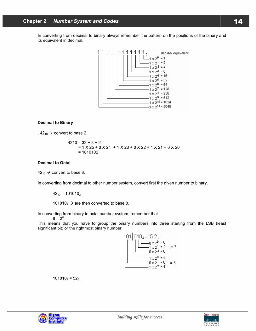
In converting from decimal to binary always remember the pattern on the positions of the binary and its equivalent in decimal.
Decimal to Binary
. 4210 � convert to base 2.
4210 = 32 + 8 + 2 = 1 X 25 + 0 X 24 + 1 X 23 + 0 X 22 + 1 X 21 + 0 X 20 = 1010102
Decimal to Octal 4210 � convert to base 8.
In converting from decimal to other number system, convert first the given number to binary.
4210 = 1010102
1010102 � are then converted to base 8.
In converting from binary to octal number system, remember that
8 = 23.
This means that you have to group the binary numbers into three starting from the LSB (least significant bit) or the rightmost binary number.
1010102 = 528

Chapter 2 Number System and Codes 15
Building skills for success
Decimal to Hexadecimal
4210 � convert to base 16. Again, in converting from decimal to other number system, convert first the given number to binary.
4210 = 1010102 1010102 � are then converted to base 16. In converting from binary to hexadecimal number system, remember that 16 = 2
4. This means that
you have to group the binary numbers into four starting from the LSB (least significant bit) or the rightmost binary number.
1010102 = 2A16
Section 2.3 Octal Number System
The octal number system has a base of eight, meaning that it has eight possible digits: 0,1,2,3,4,5,6,7.
83 82 81 80 8-1 8-2 8-3
=512 =64 =8 =1 . =1/8 =1/64 =1/512
Most Significant Digit
Octal point
Least Significant Digit
Octal to Decimal ConversionOctal to Decimal ConversionOctal to Decimal ConversionOctal to Decimal Conversion
eg. 24.68 = 2 x (81) + 4 x (8
0) + 6 x (8
-1) = 20.7510
BinaryBinaryBinaryBinary----ToToToTo----Octal / OctalOctal / OctalOctal / OctalOctal / Octal----ToToToTo----Binary ConversionBinary ConversionBinary ConversionBinary Conversion
Octal Digit 0 1 2 3 4 5 6 7
Binary Equivalent 000 001 010 011 100 101 110 111
Each Octal digit is represented by three bits of binary digit. eg. 100 111 0102 = (100) (111) (010)2 = 4 7 28

Chapter 2 Number System and Codes 16
Building skills for success
RepeatRepeatRepeatRepeatedededed Division Division Division Division
This method uses repeated division by 8. Example:. convert 17710 to octal and binary:
177/8 = 22+ remainder of 1 1 (Least Significant Bit)
22/ 8 = 2 + remainder of 6 6
2 / 8 = 0 + remainder of 2 2 (Most Significant Bit)
Result 17710 = 2618
Convert to Binary = 0101100012
Octal to HexadecimalOctal to HexadecimalOctal to HexadecimalOctal to Hexadecimal
Long method: 258 � convert to base 16
Step 1. Change first to its positional notation to find its decimal equivalent. 258 = 2 X 8
1 + 5 X 8
0
= 16 + 5 = 2110
Step 2. After getting the decimal equivalent, you can now proceed to the series of division to convert to the other base. 2110 � convert to base 16
258 = 2110 = 1516
Short Method:Short Method:Short Method:Short Method: 358 � convert to base 16
In converting from octal to hexadecimal convert first the given number to its binary equivalent. In this example, we know that the octal number is a group of three from the binary number. So to convert 358 to its binary equivalent, each digit is equal to a group of three bits.

Chapter 2 Number System and Codes 17
Building skills for success
358 = 0111012 = 1D16
Section 2.4 Hexadecimal Number System
The hexadecimal system uses base 16. Thus, it has 16 possible digit symbols. It uses the digits 0 through 9 plus the letters A, B, C, D, E, and F as the 16 digit symbols.
163 162 161 160 16-1 16-2 16-3
=4096 =256 =16 =1 . =1/16 =1/256 =1/4096
Most Significant Digit
Hexadec. point
Least Significant Digit
Hexadecimal to Decimal ConversionHexadecimal to Decimal ConversionHexadecimal to Decimal ConversionHexadecimal to Decimal Conversion
eg. 2AF16 = 2 x (162) + 10 x (16
1) + 15 x (16
0) = 68710
RepeatRepeatRepeatRepeatedededed Division: Convert decimal to hexadecimal Division: Convert decimal to hexadecimal Division: Convert decimal to hexadecimal Division: Convert decimal to hexadecimal
This method uses repeated division by 16. Example: convert 37810 to hexadecimal and binary:
378/16 = 23+ remainder of 10 A (Least Significant Bit)
23/ 16 = 1 + remainder of 7 7
1 / 16 = 0 + remainder of 1 1 (Most Significant Bit)
Result 37810 = 17A8
Convert to Binary = 0001 0111 10102 = 0000 0001 0111 1010 (16 bits)

Chapter 2 Number System and Codes 18
Building skills for success
BinaryBinaryBinaryBinary----ToToToTo----Hexadecimal /HexadecimalHexadecimal /HexadecimalHexadecimal /HexadecimalHexadecimal /Hexadecimal----ToToToTo----Binary ConversionBinary ConversionBinary ConversionBinary Conversion
Hexadecimal Digit 0 1 2 3 4 5 6 7
Binary Equivalent 0000 0001 0010 0011 0100 0101 0110 0111
Hexadecimal Digit 8 9 A B C D E F
Binary Equivalent 1000 1001 1010 1011 1100 1101 1110 1111
Each Hexadecimal digit is represented by four bits of binary digit. Example: 1011 0010 11112 = (1011) (0010) (1111)2 = B 2 F16
OctalOctalOctalOctal----ToToToTo----Hexadecimal /HexadecimalHexadecimal /HexadecimalHexadecimal /HexadecimalHexadecimal /Hexadecimal----ToToToTo----Octal ConversionOctal ConversionOctal ConversionOctal Conversion
Convert Octal (Hexadecimal) to Binary 1. First. regroup the binary number in 3 bits a group starts from the LSB if Octal is required.
Go back to Section 2.3 if you are not sure how to group in Octal. 2. Regroup the binary number in 4 bits a group from the LSB if Hexadecimal is required.
Example: Convert 5A816 to Octal .
5A816 = 0101 1010 1000 (Binary)
= 2 6 5 0 (Octal)
Another Example: 2A16 � convert to base 8. In converting from hexadecimal to octal convert first the given number to its binary equivalent. In this example, we know that the hexadecimal number is a group of four from the binary number. So to convert 2A16 to its binary equivalent, each digit is equal to a group of four binary digits (bits).
2A16 = 001010102 = 528
Chapter 2 Number System and Codes 19
Building skills for success
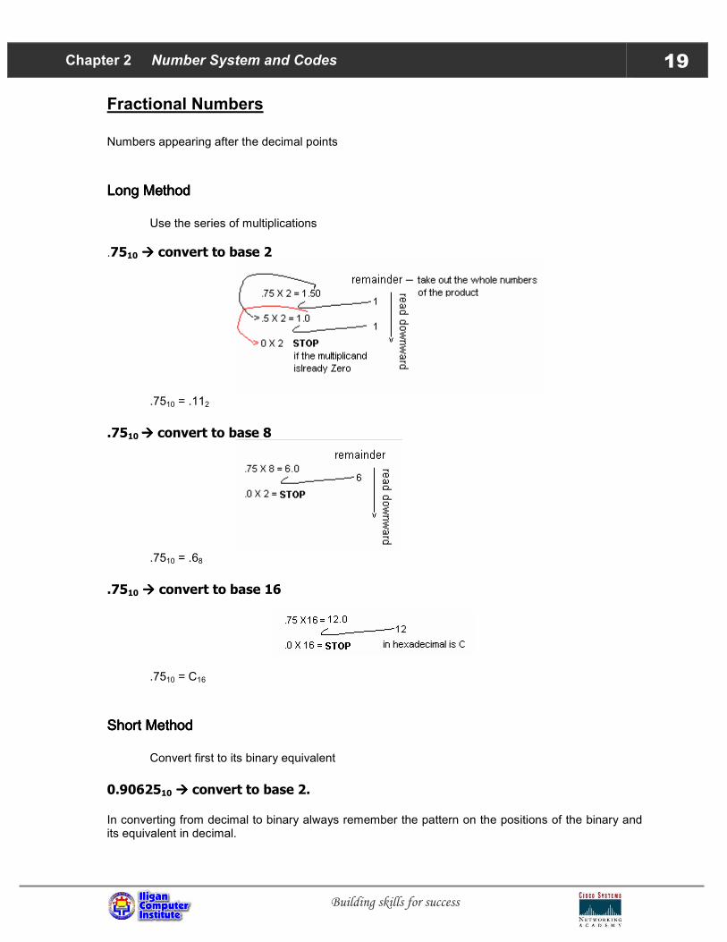
Fractional Numbers
Numbers appearing after the decimal points
Long MethodLong MethodLong MethodLong Method
Use the series of multiplications
.7510 ���� convert to base 2
.7510 = .112
.7510 ���� convert to base 8
.7510 = .68
.7510 ���� convert to base 16
.7510 = C16
Short MethodShort MethodShort MethodShort Method
Convert first to its binary equivalent
0.9062510 ���� convert to base 2. In converting from decimal to binary always remember the pattern on the positions of the binary and its equivalent in decimal.

Chapter 2 Number System and Codes 20
Building skills for success
0.9062510 = 0.5 + 0.25 + 0.125 + 0.03125 = 1 X 2
-1 + 1 X 2
-2 + 1 X 2
-3 + 0 X 2
-4 + 1 X 2
-5
= 0.111012
0.9062510 ���� convert to base 8 Convert first the given number to base 2. Which is we will have to group them from their binary form into three. 0.9062510 = 0.111012
In grouping into three, start grouping from the binary point rightward. Therefore: 0.9062510 = 0.111012 = 0.728
0.9062510 ���� convert to base 16 Convert first the given number to base 2. Which is we will have to group them from their binary form into four. 0.9062510 = 0.111012
In grouping into four, start grouping from the binary point rightward. Therefore:
0.9062510= 0.111012= 0.D816

Chapter 2 Number System and Codes 21
Building skills for success
Chapter 2Chapter 2Chapter 2Chapter 2 Self TestSelf TestSelf TestSelf Test
Choose the correct answers in the following questions.
1. Convert (63.25)10 to binary.
11111.11
111001.01
111111.01
111111.1
None of the above
2. Convert (43.8125)10 to binary.
101011.1101
110101.1101
101011.1011
110101.1011
None of the above 3. Convert (1001011.011)2 to decimal.
73.0375
75.375
91.375
75.573
None of the above 4. Convert (110101.1011)2 to decimal.
53.6875
53.6375
52.6875
55.6375
None of the above 5. Convert (11001.1)2 to base 8.
(62.4)8
(62.1)8
(31.1)8

Chapter 2 Number System and Codes 22
Building skills for success
(31.2)8
(31.4)8 6. Convert (25.6)8 to binary.
(10101.11)2
(11101.10)2
(10101.10)2
(10010.11)2
(11111.01)2
7. Convert (35.1)8 to base 16.
(17.4)16
(1D.1)16
(D1.2)16
(E8.1)16
None of the above 8. Convert (39.A)16 to base 8.
(35.5)8
(70.5)8
(71.5)8
(72.25)8
(75.5)8 9. Convert (485)10 to base 16.
(1E5)16
(231)16
(5E1)16
(15E)16
None of the above
10. Try Harder Convert (397)10 to base 3.
(12310)3
(121201)3
(012211)3
(112201)3
(100202)3

Binary Arithmetic
Binary Arithmetic s performed in the same manner as in
decimal arithmetic.
Section 3.1 Binary Addition
Any 1 in the addends of the series of binary addition, the sum is 1. But 1 + 1 = 0, causing a carry to the next significant bit a carry of 1. 0 + 0 = 0 0 + 1 = 1 1 + 0 = 1 1 + 1 = 0 with a carry of 1 Ex. 1. 810 = 10002 2. 1210 = 11002 + 510 = 01012 + 310 = 00112 ------------------ ------------------- 1310 = 11012 1510 = 11112 1 1 1 1 1 1 1
3. 1100 10002 4. 1011 11012 + 0010 10112 + 0100 10012 ------------------- ------------------- 1111 00112 1 0000 01102
Section 3.2 Binary Subtraction
0 – 0 = 0 1 – 0 = 1 1 – 1 = 0 0 – 1 = 1 with a borrow of 1 Ex. 1. 4210 = 1010102 2. 110100.0012 - 1810 = 100102 - 11011.1102 ------------------ ------------------- 2410 = 0110002 011000.0112
C H A P T E R
+ + + +
3-1 Binary Addition
3-2 Binary Addition
3-3 Binary Multiplication
3-4 Binary Division
3-5 Binary Complement
+ + + +
3333

Chapter 3 Binary Arithmetic 24
Building skills for success
Section 3.3 Binary Multiplication
Any 1 in the multiplicands or multiplier in the series of multiplication, the product is always 1. 0 * 0 = 0 0 * 1 = 0 1 * 0 = 0 1 * 1 = 1 Ex. 1. 1710 = 100012 2. 1 1 1 . 1 12 1010 = 10102 X 1 0 . 1 12
----------- ------------ ------------------- 00 00000 1 1 1 1 1 17 10001 1 1 1 1 1
------- 00000 0 0 0 0 0 17010 10001 1 1 1 1 1 ------------ ------------------- 101010102 1 0 1 0 1. 0 1 0 12
Section 3.4 Binary Division
This operation is a combination of multiplication and subtraction and follows the same rules as stated above.
Ex.
1. 04 � 0 0 0 0 1 0 0
6 / 24 110 / 0 0 0 1 1 0 0 0
24 0 0 0 1 1 0
----- -----------------
0 0 0 0 – two more zero’s will be added to the quotient
Section 3.5 Binary Complements
Two Types:
1’s Complement1’s Complement1’s Complement1’s Complement
Every 1 in a number is changed to 0 and every 0 to a 1. Ex. 111011.112 � 000100.002 The application of this is when we want to add signed numbers. The negative number is converted to its 1’s complement while the positive number maintains its binary equivalent.

Chapter 3 Binary Arithmetic 25
Building skills for success
Ex. 8910 = 0101 10012 � 0101 10012
- 6710 = 0100 00112 � + 1011 11002 ------- ------------------
2210 1 0001 0101 the carry is added to the LSB + 1 ------------------ 0001 01102 = 2210 0 means a positive number
2’s Complement2’s Complement2’s Complement2’s Complement
Every 1 in a number is changed to 0 and every 0 to a 1. A 1 is then added to the LSB (least significant bit) of the new number form.
Ex. 11 01102 � 00 1001 + 1 ------------ 00 10102 The application of this 2’s complement is when we are to add signed numbers or numbers that includes negative. Ex. –3210 = - 0010 00002 � 1101 1111 +1510 = + 0000 11112 + 1 -------- --------------- - 1710 1110 00002
The negative number will be converted to its 2’s complement and the positive number maintains its binary equivalent. 1110 00002 + 0000 11112 ------------------- 1110 11112 � 2’s complement = 0001 0000
+ 1 the MSB is 1 therefore negative -------------- - 0001 00012 = - 1710
The most significant bit (MSB) or the leftmost bit identifies weather the number is positive or negative. If the MSB is 1 the number is negative. If the MSB is 0 the number is positive.
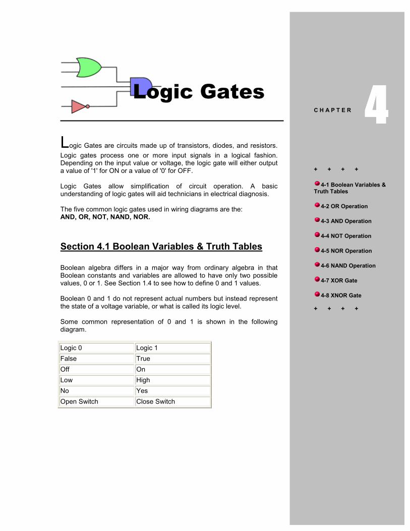
Logic Gates
Logic Gates are circuits made up of transistors, diodes, and resistors.
Logic gates process one or more input signals in a logical fashion. Depending on the input value or voltage, the logic gate will either output a value of '1' for ON or a value of '0' for OFF. Logic Gates allow simplification of circuit operation. A basic understanding of logic gates will aid technicians in electrical diagnosis. The five common logic gates used in wiring diagrams are the: AND, OR, NOT, NAND, NOR.
Section 4.1 Boolean Variables & Truth Tables
Boolean algebra differs in a major way from ordinary algebra in that Boolean constants and variables are allowed to have only two possible values, 0 or 1. See Section 1.4 to see how to define 0 and 1 values. Boolean 0 and 1 do not represent actual numbers but instead represent the state of a voltage variable, or what is called its logic level. Some common representation of 0 and 1 is shown in the following diagram.
Logic 0 Logic 1
False True
Off On
Low High
No Yes
Open Switch Close Switch
C H A P T E R
+ + + +
4-1 Boolean Variables & Truth Tables
4-2 OR Operation
4-3 AND Operation
4-4 NOT Operation
4-5 NOR Operation
4-6 NAND Operation
4-7 XOR Gate
4-8 XNOR Gate
+ + + +
4444

Chapter 4 Logic Gates 27
Building skills for success
In boolean algebra, there are three basic logic operations:
OR, AND and NOT. These logic gates are digital circuits constructed from diodes, transistors, and resistors connected in such a way that the circuit output is the result of a basic logic operation (OR, AND, NOT) performed on the inputs.
Truth TableTruth TableTruth TableTruth Table
A truth table is a means for describing how a logic circuit's output depends on the logic levels present at the circuit's inputs. In the following two-inputs logic circuit, the table lists all possible combinations of logic levels present at inputs A and B along with the corresponding output level X.
When either input A OR B is 1, the output X is 1. Therefore the "?" in the box is an OR gate. Go to next section to explore more on the OR gate.
Digital CircuitsDigital CircuitsDigital CircuitsDigital Circuits
Logic Gates are digital circuits. All digital circuits are either ON or OFF. A light switch in your house can be used as an example of a digital circuit. The light is either ON or OFF depending on the switch position. When the Light is ON the output value is '1'. When the Light is OFF the output value is '0'. The inputs are the position of the light switch. The switch is placed either in the ON or OFF position to activate the Light.
Chapter 4 Logic Gates 28
Building skills for success
Binary CodeBinary CodeBinary CodeBinary Code
Logic gates are digital circuits and they utilize a binary numbering system known as binary code. Binary code is the same language used by computers which use only 1 or 0 as numbers. People use a base 10 numbering system, ones, tens, hundreds, etc. Example: 1,2,3,4,5,6,7,8,9,and 0. Once we get to zero, we expand to the tens place: 10, 11, etc.
Binary code example:
00000001 = 1 00000010 = 2
00000011 = 3 00000100 = 4
00000101 = 5 00000110 = 6
00000111 = 7 00001000 = 8
00001001 = 9 00001010 = 10
When the number place holder is empty, it has a zero in it. When full, there is a 1. Look at the first example, the number one. When we add a 1 to the number 1, the first place holder becomes a zero and we carry one place to the left. The zero (the second from the left) now becomes a 1. So a number 10 in the binary system equals a number 2 in the base 10 system.
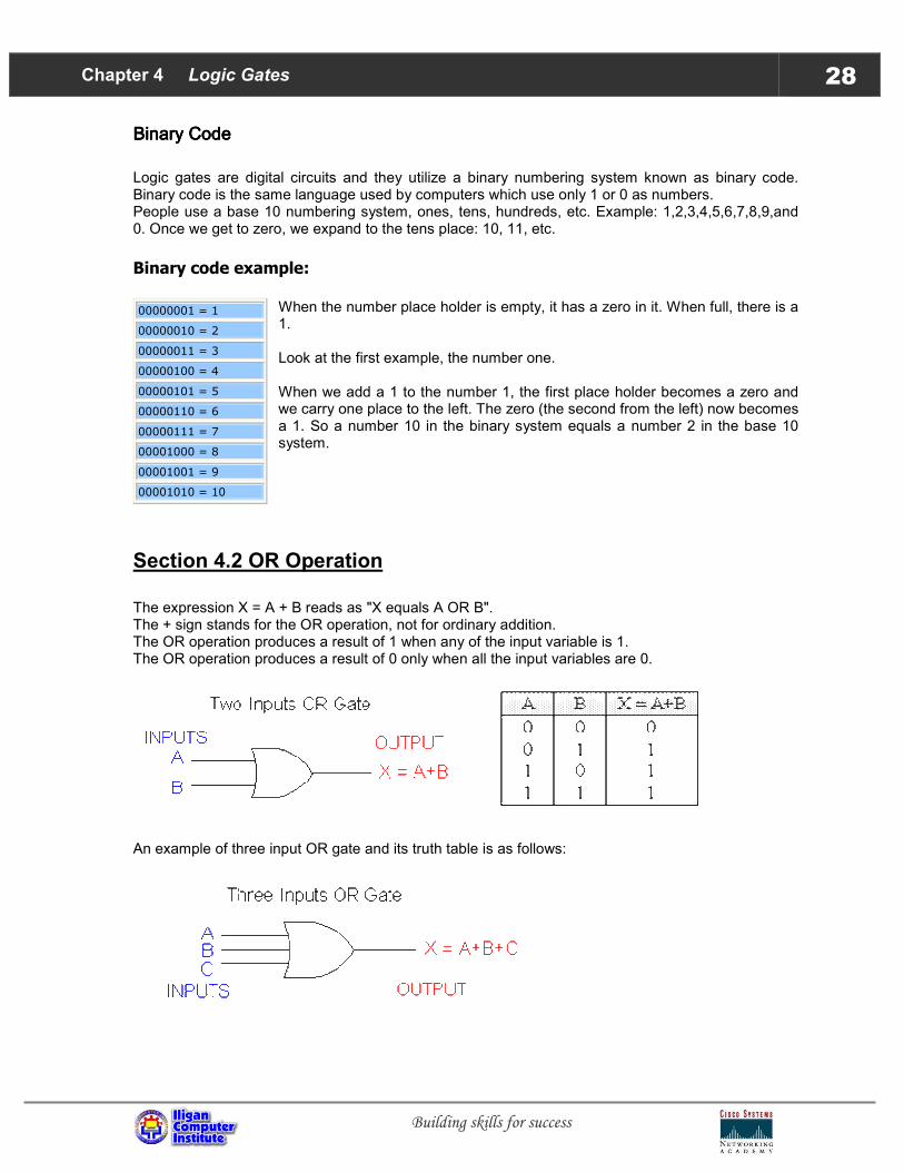
Section 4.2 OR Operation
The expression X = A + B reads as "X equals A OR B". The + sign stands for the OR operation, not for ordinary addition. The OR operation produces a result of 1 when any of the input variable is 1. The OR operation produces a result of 0 only when all the input variables are 0.
An example of three input OR gate and its truth table is as follows:

Chapter 4 Logic Gates 29
Building skills for success
With the OR operation, 1 + 1 = 1, 1+ 1 + 1 = 1 and so on.
HOW DOES THE "OR" GATHOW DOES THE "OR" GATHOW DOES THE "OR" GATHOW DOES THE "OR" GATE WORK?E WORK?E WORK?E WORK?
An 'OR' gate is like two or more switches in parallel. Only one switch needs to be closed ('ON' or a value of '1') in order to make the lamp (output C) turn 'ON' with a value of '1'.
EXAMPLE OF "OR" GATE OPERATIONEXAMPLE OF "OR" GATE OPERATIONEXAMPLE OF "OR" GATE OPERATIONEXAMPLE OF "OR" GATE OPERATION
An input value of '1' at either of the OR gate inputs will result in an output value of '1' from the OR gate, thus sending B+ to the lamp.
Input values of '0' at all inputs to the OR gate will result in an output value of '0' from the OR gate, thus preventing B+ from going to the lamp.
Chapter 4 Logic Gates 30
Building skills for success
Section 4.3 AND Operation
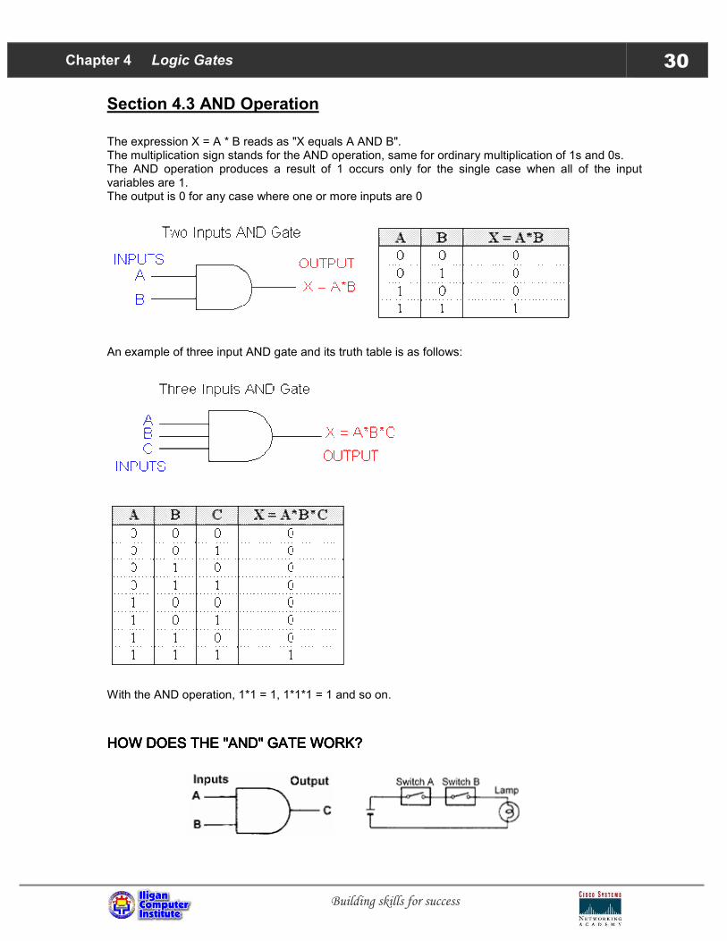
The expression X = A * B reads as "X equals A AND B". The multiplication sign stands for the AND operation, same for ordinary multiplication of 1s and 0s. The AND operation produces a result of 1 occurs only for the single case when all of the input variables are 1. The output is 0 for any case where one or more inputs are 0
An example of three input AND gate and its truth table is as follows:
With the AND operation, 1*1 = 1, 1*1*1 = 1 and so on.
HOW DOES THE "AHOW DOES THE "AHOW DOES THE "AHOW DOES THE "AND" GATE WORK?ND" GATE WORK?ND" GATE WORK?ND" GATE WORK?

Chapter 4 Logic Gates 31
Building skills for success
'AND' gates are like two or more switches in series. All the switches have to be closed ( 'ON' or a value of '1') in order to make the lamp (output C) turn on. If all inputs are not "ON", the output is "OFF".
EXAMPLE OF "AND" GATE OPERATIONEXAMPLE OF "AND" GATE OPERATIONEXAMPLE OF "AND" GATE OPERATIONEXAMPLE OF "AND" GATE OPERATION
A value of '1' is needed at all AND gate inputs to produce an output value of '1' from the AND gate, thus sending B+ to the lamp.
Unless all AND gate inputs receive a value of '1' the output value will be '0', thus preventing B+ to the lamp.
Section 4.4 NOT Operation
The NOT operation is unlike the OR and AND operations in that it can be performed on a single input variable. For example, if the variable A is subjected to the NOT operation, the result x can be expressed as
x = A' where the prime (') represents the NOT operation. This expression is read as:
x equals NOT A x equals the inverse of A x equals the complement of A
Each of these is in common usage and all indicate that the logic value of x = A' is opposite to the logic value of A.

Chapter 4 Logic Gates 32
Building skills for success
The truth table of the NOT operation is as follows:
1' = 0 because NOT 1 is 0 0' = 1 because NOT 0 is 1
The NOT operation is also referred to as inversion or complementation, and these terms are used interchangeably. NOT gates reverse the input signal value. If the input value is '1', the output value will be '0'. If the input value is '0', then the output value will be '1'. NOT gates can be referred to as inverters; whatever the input signal is the output is always the opposite.
EXAMPLE OF "NOT" GATE OPERATIONEXAMPLE OF "NOT" GATE OPERATIONEXAMPLE OF "NOT" GATE OPERATIONEXAMPLE OF "NOT" GATE OPERATION
An input value of '0' at the NOT gate produces an output value of '1' from the NOT gate, thus sending B+ to the lamp (as shown above). An input value of '1' at the NOT gate produces an output value of '0' from the NOT gate, thus preventing B+ from going to the lamp.
Section 4.5 NOR Operation
NOR and NAND gates are used extensively in digital circuitry. These gates combine the basic operations AND, OR and NOT, which make it relatively easy to describe then using Boolean Algebra. NOR is the same as the OR gate symbol except that it has a small circle on the output. This small
circle represents the inversion operation. Therefore the output expression of the two input NOR gate is:
X = ( A + B )'

Chapter 4 Logic Gates 33
Building skills for success
An example of three-input OR gate can be constructed by a NOR gate plus a NOT gate:
EXAMPLE OF "NOR" GAEXAMPLE OF "NOR" GAEXAMPLE OF "NOR" GAEXAMPLE OF "NOR" GATE OPERATIONTE OPERATIONTE OPERATIONTE OPERATION
If a value of '1' is applied to either input of the OR gate, it will produce an output value of '1' from the OR gate. The NOT gate receives an input value of '1', which is inverted by the NOT gate to an output value of '0'.

Chapter 4 Logic Gates 34
Building skills for success
If a value of '1' is applied to either input of the NOR gate, an output value of '0' will result from the NOR gate, thus preventing B+ from going to the lamp.
If a value of '0' is sent to all of the inputs of the NOR gate, the output value of '0' will result from the OR gate. The NOT gate will receive an input value of '0' which is inverted to an output value of '1'.
If a value of '0' is applied to all the NOR gate inputs, an output value of '1' will result from the NOR gate, thus sending B+ to the lamp.
Section 4.6 NAND Operation
NAND is the same as the AND gate symbol except that it has a small circle on the output. This small circle represents the inversion operation. Therefore the output expression of the two input NAND gate is:
X = ( AB )'

Chapter 4 Logic Gates 35
Building skills for success
EXAMPLE OF "NAND" GATE OPERATIONEXAMPLE OF "NAND" GATE OPERATIONEXAMPLE OF "NAND" GATE OPERATIONEXAMPLE OF "NAND" GATE OPERATION
If a value of '1' is sent to all inputs of the AND gate the result will be an output value of '1' from the AND gate. The NOT gate receives an input value of '1' and will invert the output value to '0'.
If a value of '1' is applied to all the NAND gate inputs, an output value of '0' will result from the NAND gate, thus preventing B+ to the lamp.
If a value of '0' is sent to all of the AND gate inputs, the output value of '0' will result from the AND gate. The NOT gate will receive an input value of '0', which is inverted to produce an output value of '1'. If a value of '0' is applied to all the NAND gate inputs, an output value of '1' will result from the NAND gate, thus sending B+ to the lamp.

Chapter 4 Logic Gates 36
Building skills for success
Section 4.7 XOR Gate
Exclusive OR gate has two or more input signal but only one output signal. The output is HIGH if the number of 1’s in the input is ODD. Symbol:
Truth Table:
Inputs
A B
Output
0 0 0
0 1 1
1 0 1
1 1 0
Section 4.8 XNOR Gate
Excusive NOR gate has two or more input signal but only one output signal. The output is HIGH if the number if 1’s in the input is EVEN. It is simply the opposite or inverse of the XOR gate. Symbol:
Truth Table:
Inputs
A B
Output
0 0 1
0 1 0
1 0 0
1 1 1

Chapter 4 Logic Gates 37
Building skills for success
Chapter 4 Chapter 4 Chapter 4 Chapter 4 Self TestSelf TestSelf TestSelf Test
Choose the correct answers in the following questions.
1. Boolean algebra is different from ordinary algebra in which way?
Boolean algebra can represent more than 1 discrete level between 0 and 1
Boolean algebra have only 2 discrete levels: 0 and 1
Boolean algebra can describe up to 3 levels of logic levels
They are actually the same
None of the Above
The following 2 questions are referred to the below image:
2. What is the output X if both inputs A and B are 0?
0
1
I don't know
None of the Above 3. What is the output X if A=1 and B=0?
0
1
I don't know
None of the Above 4. For a three inputs (A,B C) OR gate, what inputs are needed if output=0?
A=0, B=0, C=1
A=0, B=1, C=0
A=1, B=1, C=1
A=0, B=0,C=0
None of the Above

Chapter 4 Logic Gates 38
Building skills for success
The following 2 questions are refered to the below image:
5. What is the output X if input A=1, B=0 and C=1?
0
1
I don't know
None of the Above 6. What inputs are needed if output=1?
A=0,B=0,C=0
A=1, B=0, C=1
A=0, B=1, C=0
A=1, B=1, C=1
None of the Above
The following 2 questions are related to the below image:
7. What is the ouput of the above gate if input A=0, B=1?
0
1
Not sure
None of the Above 8. What are the value of the inputs if output=1?
A=0, B=0
A=0, B=1
A=1, B=0
A=1, B=1
I don't know

Chapter 4 Logic Gates 39
Building skills for success
The following 2 questions are related to the below image:
9. What are the values of the inputs if output=0?
A=0, B=0
A=0, B=1
A=1, B=0
A=1, B=1
I don't know 10. Try Harder For the truth table below, what typr of logic gate is it?
3 Inputs OR
3 Inputs AND
3 Inputs NOR
3 Inputs NAND
Not sure

Boolean Algebra
Section 5.1 Describing Logic Circuits Algebraically
Any logic circuit, no matter how complex, may be completely described
using the Boolean operations, because the OR gate, AND gate, and NOT circuit are the basic building blocks of digital systems. This is an example of the circuit using Boolean expression:
If an expression contains both AND and OR operations, the AND operations are performed first, like: X = AB + C; AB is performed first. Unless there are parentheses in the expression, in which case the operation inside the parentheses is to be performed first, like:
X = (A+B) + C; A+B is performed first.
C H A P T E R
+ + + +
5-1 Describing Logic Circuits Algebraically
5-2 Evaluating Logic Circuit Outputs
5-3 Implementing Circuits from Boolean Expression
5-4 Boolean Theorems
5-5 DeMorgan's Theorems
5-6 Universality of NAND and NOR Gates
5-7 Alternate Logic-Gate Representations
5-8 Logic Symbol Interpretation
+ + + +
5555

Chapter 5 Boolean Algebra 41
Building skills for success
Circuits containing InvertersCircuits containing InvertersCircuits containing InvertersCircuits containing Inverters
Whenever an INVERTER is present in a logic-circuit diagram, its output expression is simply equal to the input expression with a prime (') over it.
Section 5.2 Evaluating Logic Circuit Outputs
Once the Boolean expression for a circuit output has been obtained, the output logic level can be determined for any set of input levels. These are two examples of the evaluating logic circuit output: Let A=0, B=1, C=1, D=1
X = A'BC (A+D)'
= 0'*1*1* (0+1)'
= 1 *1*1* (1)'
= 1 *1*1* 0
= 0
Let A=0, B=0, C=1, D=1, E=1
X = [D+ ((A+B)C)'] * E
= [1 + ((0+0)1 )'] * 1
= [1 + (0*1)'] * 1
= [1+ 0'] *1
= [1+ 1 ] * 1
= 1
In general, the following rules must always be followed when evaluating a Boolean expression:
1. First, perform all inversions of single terms; that is, 0 = 1 or 1 = 0. 2. Then perform all operations within parentheses. 3. Perform an AND operation before an OR operation unless parentheses indicate otherwise. 4. If an expression has a bar over it, perform the operations of the expression first and then invert the result.
Chapter 5 Boolean Algebra 42
Building skills for success
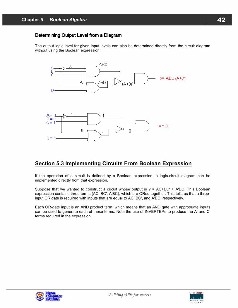
Determining Output Level from a DiagramDetermining Output Level from a DiagramDetermining Output Level from a DiagramDetermining Output Level from a Diagram
The output logic level for given input levels can also be determined directly from the circuit diagram without using the Boolean expression.
Section 5.3 Implementing Circuits From Boolean Expression
If the operation of a circuit is defined by a Boolean expression, a logic-circuit diagram can he implemented directly from that expression. Suppose that we wanted to construct a circuit whose output is y = AC+BC' + A'BC. This Boolean expression contains three terms (AC, BC', A'BC), which are ORed together. This tells us that a three-input OR gate is required with inputs that are equal to AC, BC', and A'BC, respectively. Each OR-gate input is an AND product term, which means that an AND gate with appropriate inputs can be used to generate each of these terms. Note the use of INVERTERs to produce the A' and C' terms required in the expression.

Chapter 5 Boolean Algebra 43
Building skills for success
Section 5.4 Boolean Theorems
Investigating the various Boolean theorems (rules) can help us to simplify logic expressions and logic circuits.

Chapter 5 Boolean Algebra 44
Building skills for success
Important operations: Logical Addition 0 + 0 = 0 Logical Multiplication 0 * 0 = 0 0 + 1 = 1 0 * 1 = 0 1 + 0 = 1 1 * 0 = 0 1 + 1 = 1 1 * 1 = 1 Complement - the invert or the opposite state 0’ = 1 1’ = 0
Multivariable TheoremsMultivariable TheoremsMultivariable TheoremsMultivariable Theorems
The theorems presented below involve more than one variable:
(9) x + y = y + x (commutative law)
(10) x * y = y * x (commutative law)
(11) x+ (y+z) = (x+y) +z = x+y+z (associative law)
(12) x (yz) = (xy) z = xyz (associative law)
(13a) x (y+z) = xy + xz
(13b) (w+x)(y+z) = wy + xy + wz + xz
(14) x + xy = x [proof see below]
(15) x + x'y = x + y
Boolean theorems 15 to 19 are derived from the basic rules which are from 1 – 14. The following are the solution to prove these rules. Rule 15. X + XZ = X = X (1 + Z) = X (1) = X Rule 16. X ( X + Y ) = X = XX + XY = X + XY = X (1 + Y) = X (1) = X Rule 17. ( X + Y ) ( X + Z ) = X + YZ = XX + XZ + XY + YZ = X + XZ + XY + YZ = X + XY + YZ = X + YZ

Chapter 5 Boolean Algebra 45
Building skills for success
Rule 18. X + X’Y = X + Y same as X’ + XY = X’ + Y Proving through examples: IF X = 0 ; Y = 1 IF X = 1 ; Y = O X + X’Y = 0 + ( 0’ * 1 ) X + X’Y = 1+ (1’ * 0 ) = 0 + ( 1 + 1 ) = 1 + (0 * 0 ) = 0 + 1 = 1 + 0 = 1 = 1 Which is also true that X + Y = 1 if X = 0 and Y = 1 ; X’ + Y = 0 if X = 1 and Y = 0 Rule 19. XY + YZ + Y’Z = XY + Z = XY + Z ( Y + Y’ ) rule 14 = XY + Z (1) rule 4 = XY + Z rule 6
Applications of Boolean AlgebraApplications of Boolean AlgebraApplications of Boolean AlgebraApplications of Boolean Algebra
Simplify the following expressions: 1. AB + A ( B + C ) + B ( B + C) 2. A + AB + ABC 3. ( A + B ) C + ABC
Solutions: 1. AB + A ( B + C ) + B ( B + C ) = A [B + C] + B [B + C] = [B + C] [A+B] = AB +AC + B + BC = B ( A + 1 ) + AC + BC = B + AC + BC = B [1 + C] + AC = B + AC 2. A + AB + ABC = A (1 + B) + ABC = A + ABC = A (1 + BC) = A 3. (A + B) C + ABC = AC + BC + ABC = BC (1 + A) + AC = BC + AC = C (B + A)
Prove the following identities:
Solutions:

Chapter 5 Boolean Algebra 46
Building skills for success
More Examples
Find the simplified equation. 1. X’Z + Z + X’Y = A
= Z (X’+1) + X’Y = Z + X’Y
2. X’Z + Y’Z + YZ + X’Y = B = X’Z + Z(Y’+Y) + X’Y = X’Z + Z(1) + X’Y = Z(X’+1) + X’Y = Z + X’Y
3. X’Z + Y’Z + XYZ + X’Y = C
= X’Z + Z(Y’ + XY) + X’Y = X’Z + Z(Y’ + X) + X’Y = X’Z + Y’Z + XZ + X’Y = Z(X’+X) + Y’Z + X’Y = Z(1+Y’) + X’Y = Z + X’Y
4. X’YZ’ + X’Y = D
= X’Y(Z’+1) = X’Y
5. (XY)’Z + XYZ + X’YZ’ + X’Y = E
= (X’+Y’)Z + XYZ + X’YZ’ + X’Y = X’Z + Y’Z + XYZ + X’YZ’ + X’Y = X’Z + Y’Z + XYZ + X’Y(1 +Z’) = X’Z + Y’Z + XYZ + X’Y = X’Z + Y’Z + Y(XZ+ X’) = X’Z + Y’Z + Y(Z+ X’) = X’Z + Y’Z + YZ + X’Y = X’Z + Z(Y+Y’) + X’Y = X’Z + Z + X’Y = Z(X’ + 1) + X’Y = Z +X’Y
Practice. Simplify the following equations.
1. X’Y’Z’ + X’YZ’ + XY’Z’ + XYZ’ = A find A which is the simplified equation
Chapter 5 Boolean Algebra 47
Building skills for success
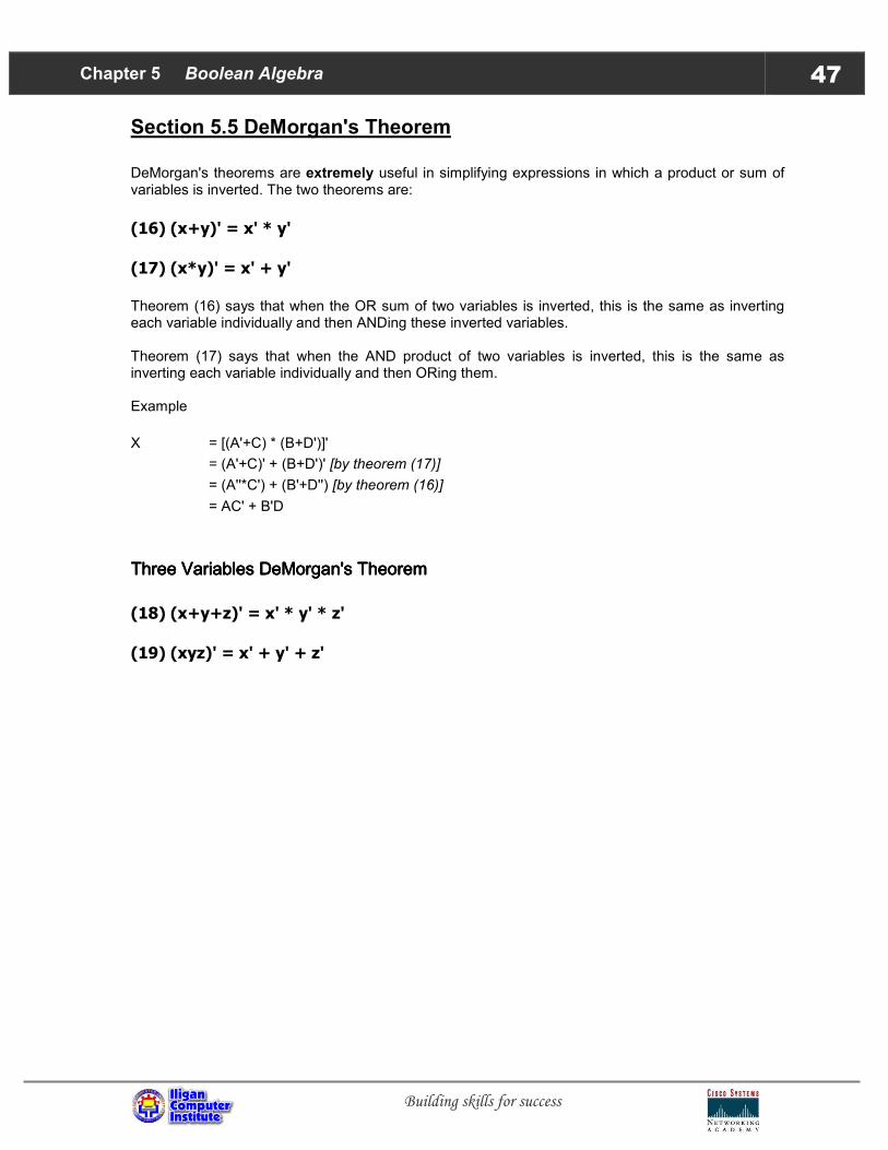
Section 5.5 DeMorgan's Theorem
DeMorgan's theorems are extremely useful in simplifying expressions in which a product or sum of variables is inverted. The two theorems are:
(16) (x+y)' = x' * y'
(17) (x*y)' = x' + y'
Theorem (16) says that when the OR sum of two variables is inverted, this is the same as inverting each variable individually and then ANDing these inverted variables. Theorem (17) says that when the AND product of two variables is inverted, this is the same as inverting each variable individually and then ORing them. Example
X = [(A'+C) * (B+D')]'
= (A'+C)' + (B+D')' [by theorem (17)]
= (A''*C') + (B'+D'') [by theorem (16)]
= AC' + B'D
Three Variables DeMorgan's TheoremThree Variables DeMorgan's TheoremThree Variables DeMorgan's TheoremThree Variables DeMorgan's Theorem
(18) (x+y+z)' = x' * y' * z'
(19) (xyz)' = x' + y' + z'

Chapter 5 Boolean Algebra 48
Building skills for success
Implications of DeMorgan's TheoremImplications of DeMorgan's TheoremImplications of DeMorgan's TheoremImplications of DeMorgan's Theorem
For (16): (x+y)' = x' * y'
For (17): (x*y)' = x' + y'
Chapter 5 Boolean Algebra 49
Building skills for success
Exercises: Solve for the simplified logic equation for the following applying De-Morgan’s Theorem. 1. AB ((ABC)’ + (AC)’ ) + (A((A(BC)’) + (AB)’)’ = X 2. (A((ABC)’ + ( A’B’) + A’)’) + ((ABC)’ (AB+C)’)’ = Y
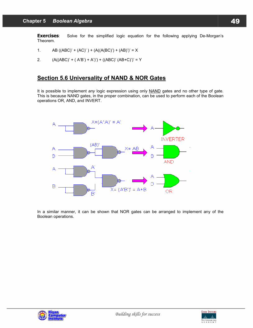
Section 5.6 Universality of NAND & NOR Gates
It is possible to implement any logic expression using only NAND gates and no other type of gate. This is because NAND gates, in the proper combination, can be used to perform each of the Boolean operations OR, AND, and INVERT.
In a similar manner, it can be shown that NOR gates can be arranged to implement any of the Boolean operations.

Chapter 5 Boolean Algebra 50
Building skills for success
Section 5.7 Alternate Logic Gate Representations
The left side of the illustration shows the standard symbol for each logic gate, and the right side shows the alternate symbol. The alternate symbol for each gate is obtained from the standard symbol by doing the following: 1. Invert each input and output of the standard symbol. This is done by adding bubbles (small circles) on input and output lines that do not have bubbles, and by removing bubbles that are already there. 2. Change the operation symbol from AND to OR, or from OR to AND. (In the special case of the INVERTER, the operation symbol is not changed.)

Chapter 5 Boolean Algebra 51
Building skills for success
Several points should be stressed regarding the logic symbol equivalences: 1. The equivalences are valid for gates with any number of inputs. 2. None of the standard symbols have bubbles on their inputs, and all the alternate symbols do. 3. The standard and alternate symbols for each gate represent the same physical circuit: there is no difference in the circuits represented by the two symbols. 4. NAND and NOR gates are inverting gates, and so both the standard and alternate symbols for each will have a bubble on either the input or the output. AND and OR gates are noninverting gates, and so the alternate symbols for each will have bubbles on both inputs and output.
Section 5.8 Logic Symbol Interpretation
Concept of Active Logic Levels:
When an input or output line on a logic circuit symbol has no bubble on it, that line is said to be
active-HIGH. When an input or output line does have a bubble on it, that line is said to be active-LOW. The presence or absence of a bubble, then, determines the active-HIGH/active-LOW status of a circuit's inputs and output, and is used to interpret the circuit operation.

Chapter 5 Boolean Algebra 52
Building skills for success
Combination of GatesCombination of GatesCombination of GatesCombination of Gates
Obtain the logical representation of the following Boolean Expression.
a)
b)
c)

Chapter 5 Boolean Algebra 53
Building skills for success
Chapter 5 Chapter 5 Chapter 5 Chapter 5 Self TestSelf TestSelf TestSelf Test
A. Choose the correct answers in the following questions.
1. What function is implemented by the circuit shown
x'y'+z
(x'+y')z
x'y'z
x'+y'+z
None of the Above 2. What function is implemented by the circuit shown
x+y+z
x+y+z'
x'y'z
x'+y'+z'
None of the Above 3. What function is implemented by the circuit shown
xz'+y
xz+y
x'z+y'
x'y'+y'z'
x'y'+y'z

Chapter 5 Boolean Algebra 54
Building skills for success
4. Which gate is the following circuit equivalent to?
AND
OR
NAND
NOR
None of the above 5. Which of the following functions equals the function: f=x+yz' ?
x(y'+z)
x(y'+z)
(y+x)(z'+x)
(y+x')(x'+z')
None of the Above 6. Any possible binary logic function can be implemented using only.
AND
OR
NOT
AA (anyone is sufficient)
NAND 7. The function in the following circuit is:
abcd
ab+cd
(a+b)(c+d)
a+b+c+d
(a'+b')(c'+d') 8. Given F=A'B+(C'+E)(D+F'), use de Morgan's theorem to find F'.
ACE'+BCE'+D'F
(A+B')(CE'D'F)

Chapter 5 Boolean Algebra 55
Building skills for success
A+B+CE'D'F
ACE'+AD'F+B'CE'+B'D'F
None of the Above 9. The function in the following circuit is:
x'+y'+z'
x+y+z
x'z'+y'z'
xy+z
z 10. Try Harder Simplify the following: {[(AB)'C]'D}'
(A'+B')C+D'
(A+B')C'+D'
A'+(B'+C')D
A'+B'+C'+D'
A+B+C+D
B. Choose the correct answers in the following questions.
1. Give the relationship that represents the dual of the Boolean property A + 1 = 1? (Note: * = AND, + = OR and ' = NOT)
a. A * 1 = 1 b. A * 0 = 0 c. A + 0 = 0 d. A * A = A e. A * 1 = 1
2. Give the best definition of a literal?
a. A Boolean variable b. The complement of a Boolean variable c. 1 or 2 d. A Boolean variable interpreted literally e. The actual understanding of a Boolean variable

Chapter 5 Boolean Algebra 56
Building skills for success
3. Simplify the Boolean expression (A+B+C)(D+E)' + (A+B+C)(D+E) and choose the best answer.
a. A + B + C b. D + E c. A'B'C' d. D'E' e. None of the above
4. Which of the following relationships represents the dual of the Boolean property x + x'y = x + y?
a. x'(x + y') = x'y' b. x(x'y) = xy c. x*x' + y = xy d. x'(xy') = x'y' e. x(x' + y) = xy
5. Given the function F(X,Y,Z) = XZ + Z(X'+ XY), the equivalent most simplified Boolean representation for F is:
a. Z + YZ b. Z + XYZ c. XZ d. X + YZ e. None of the above
6. Which of the following Boolean functions is algebraically complete?
a. F = xy b. F = x + y c. F = x' d. F = xy + yz e. F = x + y'
7. Simplification of the Boolean expression (A + B)'(C + D + E)' + (A + B)' yields which of the following results?
a. A + B b. A'B' c. C + D + E d. C'D'E' e. A'B'C'D'E'
8. Given that F = A'B'+ C'+ D'+ E', which of the following represent the only correct expression for F'?
a. F'= A+B+C+D+E b. F'= ABCDE c. F'= AB(C+D+E) d. F'= AB+C'+D'+E' e. F'= (A+B)CDE

Chapter 5 Boolean Algebra 57
Building skills for success
9. An equivalent representation for the Boolean expression A' + 1 is
a. A b. A' c. 1 d. 0
10. Simplification of the Boolean expression AB + ABC + ABCD + ABCDE + ABCDEF yields which of the following results?
a. ABCDEF b. AB c. AB + CD + EF d. A + B + C + D + E + F e. A + B(C+D(E+F))

Karnaugh Maps
Karnaugh maps provide an alternative technique for representing
Boolean functions. For example, consider the Karnaugh map for a 2-input AND gate (Figure 1).
Figure 1: Karnaugh map for a 2-input AND gate.
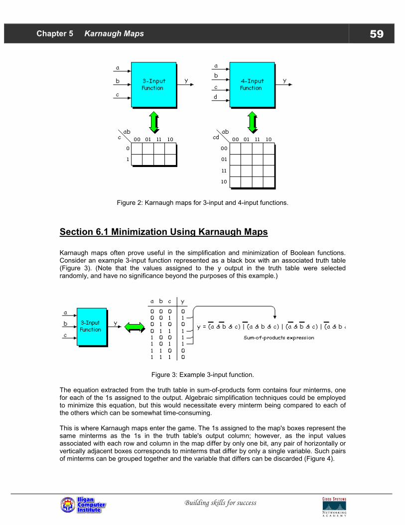
The Karnaugh map comprises a box for every line in the truth table; the binary values above the boxes are those associated with the A and B inputs. Unlike a truth table, in which the input values typically follow a standard binary sequence (00, 01, 10, 11), the Karnaugh map's input values must be ordered such that the values for adjacent columns vary by only a single bit, for example, 00, 01, 11, and 10. This ordering is known as a gray code, and it is a key factor in the way in which Karnaugh maps work. The y column in the truth table shows all the 0 and 1 values associated with the gate's output. Similarly, all of the output values could be entered into the Karnaugh map. However, for reasons of clarity, it is common for only a single set of values to be used, typically the 1s. Similar maps can be constructed for 3-input and 4-input functions (Figure 2). In the case of a 4-input map, the values associated with the c and d inputs must also be ordered as a gray code; that is, ordered in such a way that the values for adjacent rows vary by only a single bit.
C H A P T E R
+ + + +
6.1 Minimization Using Karnaugh Maps
6.2 Grouping Minterms
6.3 Incompletely Specified Functions
6.4 Populating Maps Using 0s Versus 1s + + + +
6666
Chapter 5 Karnaugh Maps 59
Building skills for success
Figure 2: Karnaugh maps for 3-input and 4-input functions.
Section 6.1 Minimization Using Karnaugh Maps
Karnaugh maps often prove useful in the simplification and minimization of Boolean functions. Consider an example 3-input function represented as a black box with an associated truth table (Figure 3). (Note that the values assigned to the y output in the truth table were selected randomly, and have no significance beyond the purposes of this example.)
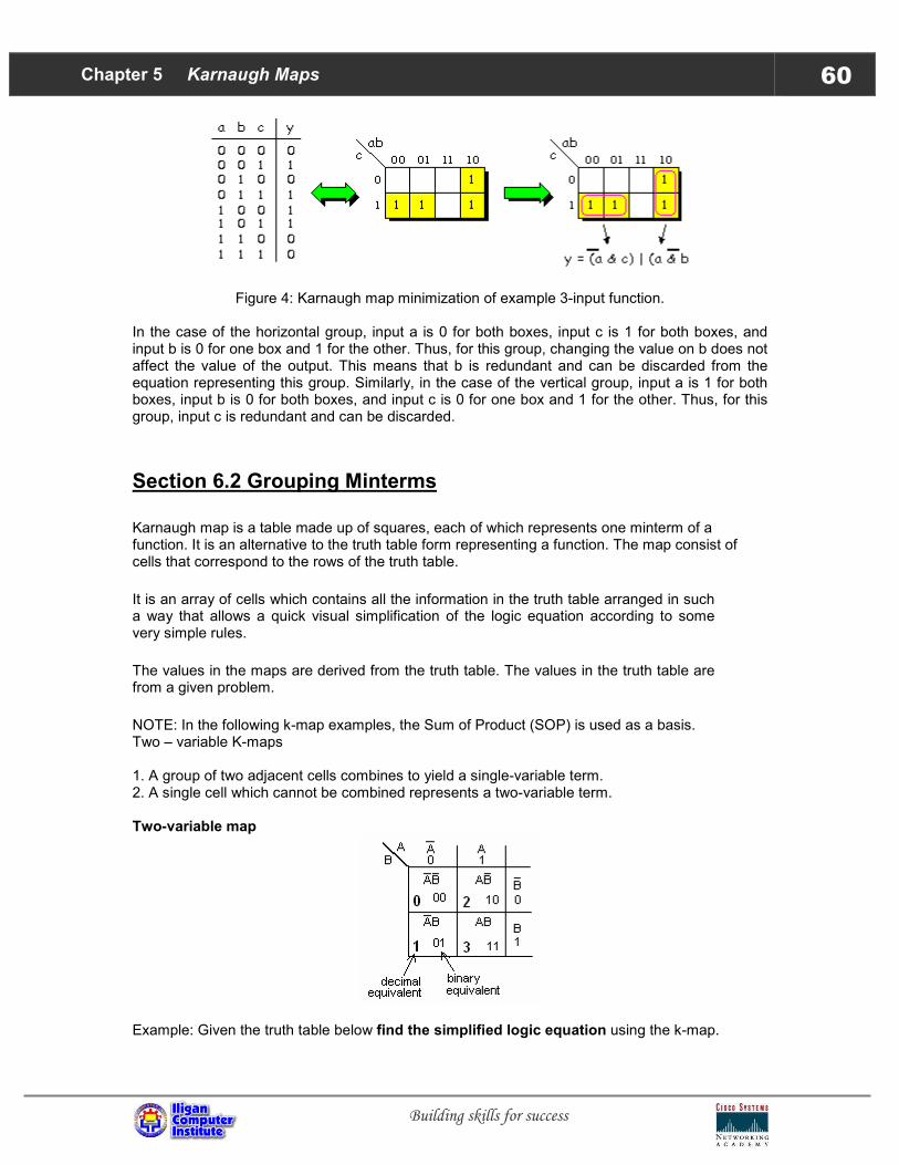
Figure 3: Example 3-input function. The equation extracted from the truth table in sum-of-products form contains four minterms, one for each of the 1s assigned to the output. Algebraic simplification techniques could be employed to minimize this equation, but this would necessitate every minterm being compared to each of the others which can be somewhat time-consuming. This is where Karnaugh maps enter the game. The 1s assigned to the map's boxes represent the same minterms as the 1s in the truth table's output column; however, as the input values associated with each row and column in the map differ by only one bit, any pair of horizontally or vertically adjacent boxes corresponds to minterms that differ by only a single variable. Such pairs of minterms can be grouped together and the variable that differs can be discarded (Figure 4).
Chapter 5 Karnaugh Maps 60
Building skills for success
Figure 4: Karnaugh map minimization of example 3-input function. In the case of the horizontal group, input a is 0 for both boxes, input c is 1 for both boxes, and input b is 0 for one box and 1 for the other. Thus, for this group, changing the value on b does not affect the value of the output. This means that b is redundant and can be discarded from the equation representing this group. Similarly, in the case of the vertical group, input a is 1 for both boxes, input b is 0 for both boxes, and input c is 0 for one box and 1 for the other. Thus, for this group, input c is redundant and can be discarded.
Section 6.2 Grouping Minterms
Karnaugh map is a table made up of squares, each of which represents one minterm of a function. It is an alternative to the truth table form representing a function. The map consist of cells that correspond to the rows of the truth table.
It is an array of cells which contains all the information in the truth table arranged in such a way that allows a quick visual simplification of the logic equation according to some very simple rules.
The values in the maps are derived from the truth table. The values in the truth table are from a given problem.
NOTE: In the following k-map examples, the Sum of Product (SOP) is used as a basis. Two – variable K-maps 1. A group of two adjacent cells combines to yield a single-variable term. 2. A single cell which cannot be combined represents a two-variable term. Two-variable map
Example: Given the truth table below find the simplified logic equation using the k-map.

Chapter 5 Karnaugh Maps 61
Building skills for success
Truth table:
Inputs
A B
Output X= ?
0 0 1
0 1 0
1 0 1
1 1 1
Solutions: The locations with values of x = 1 must be marked on the map.
Answer: X = A + B’ or X = B’ + A (cumulative property of addition).
Three – variable K-maps 1. A group of four adjacent cells (in line or in square) combines to yield a single-variable term. 2. A group of two adjacent cells combines to yield a two-variable term. 3. A single cell, which cannot be combined represent a three-variable term. Three-variable map
Example: Given the truth table below find the simplified logic equation using the k-map. Truth table:
Inputs
A B C
OutputX = ?
0 0 0 0
0 0 1 1
0 1 0 1
0 1 1 0
1 0 0 1
1 0 1 1
1 1 0 1
1 1 1 1
Solutions: The locations with values of x = 1 must be marked on the map.
Answer: X = A + BC’ + B’C or X = BC’ + A + B’C or in any arrangement as to whatever pairs comes first because of the cumulative property of addition.

Chapter 5 Karnaugh Maps 62
Building skills for success
Four – variable K-maps 1. Eight adjacent cells combine to yield a singe-variable term. 2. Four adjacent cells combine to yield a two-variable term. 3. Two adjacent cells combine to yield a three-variable term. 4. Individual cells represent a four variable term. Four-variable map
Example: Given the truth table below find the simplified logic equation using the k-map. Truth table:
Inputs
A B C D
Output X = ?
0 0 0 0 1
0 0 0 1 1
0 0 1 0 1
0 0 1 1 0
0 1 0 0 0
0 1 0 1 1
0 1 1 0 1
0 1 1 1 0
1 0 0 0 1
1 0 0 1 1
1 0 1 0 1
1 0 1 1 0
1 1 0 0 0
1 1 0 1 0
1 1 1 0 1
1 1 1 1 0
Solutions: The locations with values of X = 1 must be marked on the map.
Answer: X = A’C’B’ + B’C’ + CD’ or X = CD’ + A’C’B’ + B’C’ or in any arrangement as to whatever pairs comes first because of the cumulative property of addition

Chapter 6 Karnaugh Maps 63
Building skills for success
More examples: Simplify the following equations using k-maps. 1. X = A’B’C + AD’ + ABCD + A’ + A’BD’ 2. X = (ABCD)’ + ((AB)’ (ABC’ + (AD)’) 3. A girl (G) and a boy (B) argued if they are to go home after the party. They have decided that if both or none of them agreed, then they will go home. Find the SLE using K-map in SOP. 4. A princess wanted to choose from her 16 prince charming with the following qualities: Handsome – 30% Intelligent – 35% Wealth – 10% Healthy Body – 25%. She will only choose if the guy gets 70% or better from the given qualities. Find the truth table, SLE through K – map, and logic circuit connections. 5. Your mother decided to give you a present if you have passed at least two of your major exams (Prelim, Midterm, and Semi – Final). Find the truth table.
Product of Sum Representations (POS) In POS the binary 1 represents a complemented quantity and the binary 0 represents a not complemented quantity. Also in POS we are using the maxterms. In other words, in POS it is the summation of maxterms of the quantities. A four-variable POS map using maxterms:

Chapter 6 Karnaugh Maps 64
Building skills for success
Examples: 1. X = (A’+B+C’+D)(A’+B’)(A’+B’+D’) simplify the logic equation.
X = (A’+B’)(A’+C’+D) 2. Find the simplified logic given the map.
X = (A+B+C)(C’+D’)(A’+B+D)

Chapter 6 Karnaugh Maps 65
Building skills for success
More on Minterms & Maxterms 1. From a particular table the minterms of f(A,B,C,D) = ∑m (0,1,2,3,6,9,11,12,14,15) was derived. Obtain its simplified minterm equation. Solutions:
X=A’B’ + B’D + A’CD’ + ACD + ABD’
2. From a particular table the maxterm of f(A,B,C,D) = ∏ M(1,2,5,7,8,11,12,15) was derived. Obtain its simplified maxterm equation. Solutions:
X = (C’+D’)(A+C+D’)(A+B+C’)(A’+C+D) n the case of a 3-input Karnaugh map, any two horizontally or vertically adjacent minterms, each composed of three variables, can be combined to form a new product term composed of only two variables. Similarly, in the case of a 4-input map, any two adjacent minterms, each composed of four variables, can be combined to form a new product term composed of only three variables. Additionally, the 1s associated with the minterms can be used to form multiple groups. For example, consider a new 3-input function (Figure 5).

Chapter 6 Karnaugh Maps 66
Building skills for success
Figure 5: Karnaugh map minterms can be used to form multiple groups. Groupings can also be formed from four adjacent minterms in which case two redundant variables can be discarded; consider some 4-input Karnaugh map examples (Figure 6). In fact, any group of 2n adjacent minterms can be gathered together, where n is a positive integer. For example, 21 = two minterms, 22 = four minterms, 23 = eight minterms, and so forth.
Figure 6: Some example Karnaugh map groupings of four adjacent minterms. As was noted above, Karnaugh map input values are ordered so that the values associated with adjacent rows and columns differ by only a single bit. One result of this ordering is that the top and bottom rows are also only separated by a single bit; similarly, the left and right columns are only separated by a single bit. It may help to visualize the map rolled into a horizontal cylinder such that the top and bottom edges are touching, or into a vertical cylinder such that the left and right edges are touching. This leads to some additional grouping possibilities (Figure 7).

Chapter 6 Karnaugh Maps 67
Building skills for success
Figure 7: Some additional Karnaugh map grouping possibilities. Note especially the last example. Diagonally adjacent minterms generally cannot be used to form a group; however, remembering that the left-right columns and the top-bottom rows are logically adjacent, the four corner minterms can be used to form a single group.
Section 6.3 Incompletely Specified Functions
In certain cases a function may be incompletely specified; that is, the output may be undefined for some of the input combinations. If the designer knows that certain input combinations will never occur, then the value assigned to the output for these combinations is irrelevant. Alternatively, for some input combinations the designer may simply not care about the value on the output. In both cases, the designer can represent the output values associated with the relevant input combinations as question marks in the map (Figure 8).

Chapter 6 Karnaugh Maps 68
Building skills for success
Figure 8: Karnaugh map for an incompletely specified function. The “?” characters indicate don't care states which can be considered to represent either 0 or 1 values at the designer's discretion. It should be noted that many electronics references use X characters to represent don't care states. Unfortunately, this may lead to confusion as design tools such as logic simulators use X characters to represent don't know states. Unless otherwise indicated, this book uses “?” and “X” to represent don't care and don't know states respectively.
Incompletely Specified Functions do not affect the equations but it will only help to maximize the number of groupings.
Examples:
1. f (A, B, C, D) = ∏M (1, 4, 7, 11, 15) + d(2, 4,6, 8, 10)
X = (A+B’)(A+C+D’)(A’+C’+D’)
2. f (A, B, C, D) = ∑m (2, 5, 8, 10, 12) + d(1, 3, 5, 7, 9)

Chapter 6 Karnaugh Maps 69
Building skills for success
X = AC’ + C’D + + B’CD’
Section 6.4 Populating Maps Using 0s Versus 1s
When a Karnaugh map is populated using the 1s assigned to the truth table's output, the resulting Boolean expression is extracted from the map in sum-of-products form. As an alternative, the Karnaugh map can be populated using the 0s assigned to the truth table's output. In this case, groupings of 0's are used to generate expressions in product-of-sums format (Figure 9). Although the sum-of-products and product-of-sums expressions appear to be somewhat different, they do produce identical results. The expressions can be shown to be equivalent using algebraic means, or by constructing truth tables for each expression and comparing the outputs.
Figure 9: Karnaugh maps populated using 0s versus 1s. Karnaugh maps are most often used to represent 3-input and 4-input functions. It is possible to create similar maps for 5-input and 6-input functions, but these maps can become unwieldy and difficult to use. The Karnaugh technique is generally not considered to have any application for functions with more than six inputs.

Flip Flops
Introduction
Combinational logic refers to circuits whose output is strictly
depended on the present value of the inputs. As soon as inputs are changed, the information about the previous inputs is lost, that is, combinational logics circuits have no memory. In many applications, information regarding input values at a certain instant of time is required at some future time. Although every digital system is likely to have combinational circuits, most systems encountered in practice also include memory elements, which require that the system be described in terms of sequential logic. Circuits whose outputs depends not only on the present input value but also the past input value are known as sequential logic circuits. The mathematical model of a sequential circuit is usually referred to as a sequential machine. A general block diagram of a sequential circuit is shown below in Figure 1.
Figure 1. Block Diagram of Sequential Circuit.
C H A P T E R
+ + + +
8.1 Synchronous and Asynchronous Operation
8.2 Edge-Triggered Flip-flops
8.3 Summary of the Types of Flip-flop Behaviour
7.4 Pulse-Triggered (Master-Slave) Flip-flops
7.5 Data Lock-Out Flip-flops
7.6 Operating Characteristics
+ + + +
7777

Chapter 7 Flip Flops 71
Building skills for success
The diagram consists of combinational circuit to which memory elements are connected to form a feedback path. The memory elements are devices capable of storing binary information within them. The combinational part of the circuit receives two sets of input signals: one is primary (coming from the circuit environment) and secondary (coming from memory elements). The particular combination of secondary input variables at a given time is called the present state of the circuit. The secondary input variables are also know as the state variables. The block diagram shows that the external outputs in a sequential circuit are a function not only of external inputs but also of the present state of the memory elements. The next state of the memory elements is also a function of external inputs and the present state. Thus a sequential circuit is specified by a time sequence of inputs, outputs, and internal states.
Quiz Quiz Quiz Quiz 7777....1111
These short quizzes are to refresh on what you have learnt so far.
1. A sequential circuit is a digital circuit whose logic states depend on a specified time sequence.
True False
2. Sequential circuits contain only combinational logics.
True False
3. Sequential circuits contain memory and combinational circuits do not.
True False
4. The outputs of a sequential circuit are computed using both the present and past input values.
True False
Section 7.1 Synchronous and Asynchronous Operation
Sequential circuits are divided into two main types: synchronous and asynchronous. Their classification depends on the timing of their signals. Synchronous sequential circuits change their states and output values at discrete instants of time, which are specified by the rising and falling edge of a free-running clock signal. The clock signal is generally some form of square wave as shown in Figure 2 below.
Figure 2. Clock Signal
Chapter 7 Flip Flops 72
Building skills for success
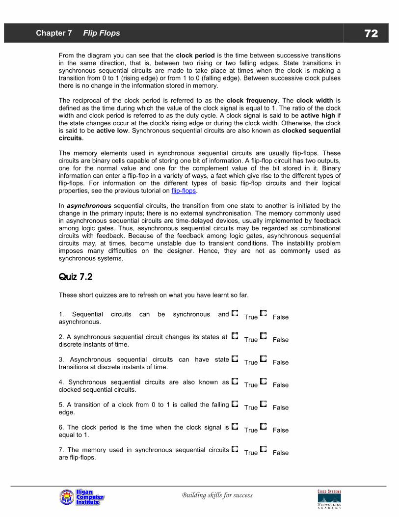
From the diagram you can see that the clock period is the time between successive transitions in the same direction, that is, between two rising or two falling edges. State transitions in synchronous sequential circuits are made to take place at times when the clock is making a transition from 0 to 1 (rising edge) or from 1 to 0 (falling edge). Between successive clock pulses there is no change in the information stored in memory. The reciprocal of the clock period is referred to as the clock frequency. The clock width is defined as the time during which the value of the clock signal is equal to 1. The ratio of the clock width and clock period is referred to as the duty cycle. A clock signal is said to be active high if the state changes occur at the clock's rising edge or during the clock width. Otherwise, the clock is said to be active low. Synchronous sequential circuits are also known as clocked sequential circuits. The memory elements used in synchronous sequential circuits are usually flip-flops. These circuits are binary cells capable of storing one bit of information. A flip-flop circuit has two outputs, one for the normal value and one for the complement value of the bit stored in it. Binary information can enter a flip-flop in a variety of ways, a fact which give rise to the different types of flip-flops. For information on the different types of basic flip-flop circuits and their logical properties, see the previous tutorial on flip-flops. In asynchronous sequential circuits, the transition from one state to another is initiated by the change in the primary inputs; there is no external synchronisation. The memory commonly used in asynchronous sequential circuits are time-delayed devices, usually implemented by feedback among logic gates. Thus, asynchronous sequential circuits may be regarded as combinational circuits with feedback. Because of the feedback among logic gates, asynchronous sequential circuits may, at times, become unstable due to transient conditions. The instability problem imposes many difficulties on the designer. Hence, they are not as commonly used as synchronous systems.
Quiz Quiz Quiz Quiz 7777....2222
These short quizzes are to refresh on what you have learnt so far.
1. Sequential circuits can be synchronous and asynchronous.
True False
2. A synchronous sequential circuit changes its states at discrete instants of time.
True False
3. Asynchronous sequential circuits can have state transitions at discrete instants of time.
True False
4. Synchronous sequential circuits are also known as clocked sequential circuits.
True False
5. A transition of a clock from 0 to 1 is called the falling edge.
True False
6. The clock period is the time when the clock signal is equal to 1.
True False
7. The memory used in synchronous sequential circuits are flip-flops.
True False

Chapter 7 Flip Flops 73
Building skills for success
Flip-flops are synchronous bistable devices. The term synchronous means the output changes state only when the clock input is triggered. That is, changes in the output occur in synchronization with the clock. Flip-flop is a kind of multivibrator. There are three types of multivibrators: Monostable multivibrator (also called one-shot) has only one stable state. It produces a single pulse in response to a triggering input. Bistable multivibrator exhibits two stable states. It is able to retain the two SET and RESET states indefinitely. It is commonly used as a basic building block for counters, registers and memories. Astable multivibrator has no stable state at all. It is used primarily as an oscillator to generate periodic pulse waveforms for timing purposes. In this tutorial, the three basic categories of bistable elements are emphasized: edge-triggered flip-flop, pulse-triggered (master-slave) flip-flop, and data lock-out flip-flop. Their operating characteristics and basic applications will also be discussed.
Section 7.2 Edge-Triggered Flip-flops
An edge-triggered flip-flop changes states either at the positive edge (rising edge) or at the negative edge (falling edge) of the clock pulse on the control input. The three basic types are introduced here: S-R, J-K and D. The S-R, J-K and D inputs are called synchronous inputs because data on these inputs are transferred to the flip-flop's output only on the triggering edge of the clock pulse.On the other hand, the direct set (SET) and clear (CLR) inputs are called asynchronous inputs, as they are inputs that affect the state of the flip-flop independent of the clock. For the synchronous operations to work properly, these asynchronous inputs must both be kept LOW.
EdgeEdgeEdgeEdge----triggered Striggered Striggered Striggered S----R flipR flipR flipR flip----flop flop flop flop
The basic operation is illustrated below, along with the truth table for this type of flip-flop. The operation and truth table for a negative edge-triggered flip-flop are the same as those for a positive except that the falling edge of the clock pulse is the triggering edge.
As S = 1, R = 0. Flip-flop SETS on the rising clock edge.

Chapter 7 Flip Flops 74
Building skills for success
Note that the S and R inputs can be changed at any time when the clock input is LOW or HIGH (except for a very short interval around the triggering transition of the clock) without affecting the output. This is illustrated in the timing diagram below:
EdgeEdgeEdgeEdge----triggered Jtriggered Jtriggered Jtriggered J----K flipK flipK flipK flip----flop flop flop flop
The J-K flip-flop works very similar to S-R flip-flop. The only difference is that this flip-flop has NO invalid state. The outputs toggle (change to the opposite state) when both J and K inputs are HIGH. The truth table is shown below.
EdgeEdgeEdgeEdge----triggered D fliptriggered D fliptriggered D fliptriggered D flip----flop flop flop flop
The operations of a D flip-flop is much more simpler. It has only one input addition to the clock. It is very useful when a single data bit (0 or 1) is to be stored. If there is a HIGH on the D input when a clock pulse is applied, the flip-flop SETs and stores a 1. If there is a LOW on the D input when a clock pulse is applied, the flip-flop RESETs and stores a 0. The truth table below summarize the operations of the positive edge-triggered D flip-flop. As before, the negative edge-triggered flip-flop works the same except that the falling edge of the clock pulse is the triggering edge.

Chapter 7 Flip Flops 75
Building skills for success
Section 7.3 Summary of the Types of Flip-flop Behaviour
Since memory elements in sequential circuits are usually flip-flops, it is worth summarising the behaviour of various flip-flop types before proceeding further. All flip-flops can be divided into four basic types: SR, JK, D and T. They differ in the number of inputs and in the response invoked by different value of input signals. The four types of flip-flops are defined in Table 1. Table 1. Flip-flop Types
FLIP-FLOP NAME
FLIP-FLOP SYMBOL
CHARACTERISTIC TABLE
CHARACTERISTIC EQUATION
EXCITATION TABLE
SR
S R Q(next)
0 0 Q
0 1 0
1 0 1
1 1 ?
Q(next) = S + R'Q SR = 0
Q Q(next) S R
0 0 0 X
0 1 1 0
1 0 0 1
1 1 X 0
JK
J K Q(next)
0 0 Q
0 1 0
1 0 1
1 1 Q'
Q(next) = JQ' + K'Q
Q Q(next) J K
0 0 0 X
0 1 1 X
1 0 X 1
1 1 X 0
D
D Q(next)
0 0
1 1
Q(next) = D
Q Q(next) D
0 0 0
0 1 1
1 0 0
1 1 1
Each of these flip-flops can be uniquely described by its graphical symbol, its characteristic table, its characteristic equation or excitation table. All flip-flops have output signals Q and Q'.
The characteristic table in the third column of Table 1 defines the state of each flip-flop as a function of its inputs and previous state. Q refers to the present state and Q(next) refers to the next state after the occurrence of the clock pulse. The characteristic table for the RS flip-flop shows that the next state is equal to the present state when both inputs S and R are equal to 0. When R=1, the next clock pulse clears the flip-flop. When S=1, the flip-flop output Q is set to 1. The equation mark (?) for the next state when S and R are both equal to 1 designates an indeterminate next state. The characteristic table for the JK flip-flop is the same as that of the RS when J and K are replaced by S and R respectively, except for the indeterminate case. When both J and K are equal to 1, the next state is equal to the complement of the present state, that is, Q(next) = Q'.

Chapter 7 Flip Flops 76
Building skills for success
The next state of the D flip-flop is completely dependent on the input D and independent of the present state. The characteristic table is useful during the analysis of sequential circuits when the value of flip-flop inputs are known and we want to find the value of the flip-flop output Q after the rising edge of the clock signal. As with any other truth table, we can use the map method to derive the characteristic equation for each flip-flop, which are shown in the third column of Table 1. During the design process we usually know the transition from present state to the next state and wish to find the flip-flop input conditions that will cause the required transition. For this reason we will need a table that lists the required inputs for a given change of state. Such a list is called the excitation table, which is shown in the fourth column of Table 1. There are four possible transitions from present state to the next state. The required input conditions are derived from the information available in the characteristic table. The symbol X in the table represents a "don't care" condition, that is, it does not matter whether the input is 1 or 0.
Quiz Quiz Quiz Quiz 7777....3333
These short quizzes are to refresh on what you have learnt so far.
1. A JK flip-flop is presently in the RESET state and must go to the SET state on the next clock pulse. J must be 1 and K must be X (don't care).
True False
2. A JK flip-flop is presently in the SET state and must remain SET on the next clock pulse. Then J must be X and K must be 1.
True False
3. A RS flip-flop is presently in a SET state and must go to the RESET state on the next clock pulse. S must be 1 and R must be 0.
True False
4. For a D flip-flop, the next state is always equal to the D input.
True False
5. For a D flip-flop, when the present state Q=0 goes to the next state Q=1, the required D input is D=1
True False
Section 7.4 Pulse-Triggered (Master-Slave) Flip-flops
The term pulse-triggered means that data are entered into the flip-flop on the rising edge of the clock pulse, but the output does not reflect the input state until the falling edge of the clock pulse. As this kind of flip-flops are sensitive to any change of the input levels during the clock pulse is still HIGH, the inputs must be set up prior to the clock pulse's rising edge and must not be changed before the falling edge. Otherwise, ambiguous results will happen. The three basic types of pulse-triggered flip-flops are S-R, J-K and D. Their logic symbols are shown below. Notice that they do not have the dynamic input indicator at the clock input but have postponed output symbols at the outputs.

Chapter 7 Flip Flops 77
Building skills for success
The truth tables for the above pulse-triggered flip-flops are all the same as that for the edge-triggered flip-flops, except for the way they are clocked. These flip-flops are also called Master-Slave flip-flops simply because their internal construction are divided into two sections. The slave section is basically the same as the master section except that it is clocked on the inverted clock pulse and is controlled by the outputs of the master section rather than by the external inputs. The logic diagram for a basic master-slave S-R flip-flop is shown below.
Secion 7.5 Data Lock-Out Flip-flops
The data lock-out flip-flop is similar to the pulse-triggered (master-slave) flip-flop except it has a dynamic clock input. The dynamic clock disables (locks out) the data inputs after the rising edge of the clock pulse. Therefore, the inputs do not need to be held constant while the clock pulse is HIGH. The master section of this flip-flop is like an edge-triggered device. The slave section becomes a pulse-triggered device to produce a postponed output on the falling edge of the clock pulse. The logic symbols of S-R, J-K and D data lock-out flip-flops are shown below. Notice they all have the dynamic input indicator as well as the postponed output symbol.
Again, the above data lock-out flip-flops have same the truth tables as that for the edge-triggered flip-flops, except for the way they are clocked.

Chapter 7 Flip Flops 78
Building skills for success
Section 7.6 Operating Characteristics
The operating characteristics mention here apply to all flip-flops regardless of the particular form of the circuit. They are typically found in data sheets for integrated circuits. They specify the performance, operating requirements, and operating limitations of the circuit. Propagation Delay Time - is the interval of time required after an input signal has been applied for the resulting output change to occur. Set-Up Time - is the minimum interval required for the logic levels to be maintained constantly on the inputs (J and K, or S and R, or D) prior to the triggering edge of the clock pulse in order for the levels to be reliably clocked into the flip-flop. Hold Time - is the minimum interval required for the logic levels to remain on the inputs after the triggering edge of the clock pulse in order for the levels to be reliably clocked into the flip-flop. Maximum Clock Frequency - is the highest rate that a flip-flop can be reliably triggered. Power Dissipation - is the total power consumption of the device. Pulse Widths - are the minimum pulse widths specified by the manufacturer for the Clock, SET and CLEAR inputs.
Registers and
Counters
A register is a group of memory element that works together
as a unit. The simplest register does nothing more than to store a binary word; others modify the stored word or shifting its bits left or right or by performing other operations to be discussed in this chapter. A counter is a special kind of register, designed to count the number of clock pulses arriving at its input. This chapter discusses some basic registers and counters used in microcomputers.
Section 8.1 Buffer Registers
A buffer register is the simplest kind of register; all it does is to store a digital word.
Basic IdeaBasic IdeaBasic IdeaBasic Idea
Figure 8-1 shows a buffer register built with positive edge triggered D-flip flops. The X bits set up the flip flops for loading. Therefore, when the first positive clock edge arrives, the stored word becomes Q3Q2Q1Q0 = X3X2X1X0. In chunked notation, Q = X The circuit is too primitive to be of any use. What it needs is some control over the X bits some way of holding them off until we’re ready to store them.
C H A P T E R
+ + + +
8-1 Buffer Registers
8-2 Shift Registers
8-4 Ripple Counters
8-5 Synchronous Counters
8-6 Ring Counters
8-7 Other Counters: Mod10 Counter
Down Counter UP-Down Counter Presettable Counter
+ + + +
8888

Chapter 8 Registers and Counters 80
Building skills for success
Figure 8-1 Buffer register
ControlledControlledControlledControlled
Figure 8-2 Controlled Buffer Register
Figure 8-2 is more like it. This is a controlled buffer register with an active-high CLR. Therefore, when CLR goes high, all flip flops reset and the stored word becomes Q = 0000 When CLR returns to Low, the register is ready for action. LOAD is a control input; it determines what the circuit does. When the LOAD is Low, the X bits cannot reach the flip flops. At the same time, the inverted signal LOAD is high this forces each flip flop output to feed back to its data input. When each rising clock edge arrives, data is circulated or retained. In other words, the register contents are unchanged when LOAD is low. When LOAD goes high, the X bits are transmitted to the data inputs. After a short time, the flip flops are ready for loading. With the arrival of the positive clock edge, the X bits are loaded and the stored word becomes
Q3Q2Q1Q0 = X3X2X1X0
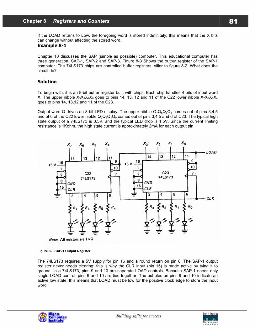
Chapter 8 Registers and Counters 81
Building skills for success
If the LOAD returns to Low, the foregoing word is stored indefinitely; this means that the X bits can change without affecting the stored word.
Example 8-1
Chapter 10 discusses the SAP (simple as possible) computer. This educational computer has three generation, SAP-1, SAP-2 and SAP-3. Figure 8-3 Shows the output register of the SAP-1 computer. The 74LS173 chips are controlled buffer registers, siilar to figure 8-2. What does the circuit do?
Solution To begin with, it is an 8-bit buffer register built with chips. Each chip handles 4 bits of input word X. The upper nibble X3X2X1X0 goes to pins 14, 13, 12 and 11 of the C22 lower nibble X7X6X5X4 goes to pins 14, 13,12 and 11 of the C23. Output word Q drives an 8-bit LED display. The upper nibble Q7Q6Q5Q4 comes out of pins 3,4,5 and of 6 of the C22 lower nibble Q3Q2Q1Q0 comes out of pins 3,4,5 and 6 of C23. The typical high state output of a 74LS173 is 3.5V, and the typical LED drop is 1.5V. Since the current limiting resistance is 1Kohm, the high state current is approximately 2mA for each output pin.
Figure 8-3 SAP-1 Output Register
The 74LS173 requires a 5V supply for pin 16 and a round return on pin 8. The SAP-1 output register never needs clearing; this is why the CLR input (pin 15) is made active by tying it to ground. In a 74LS173, pins 9 and 10 are separate LOAD controls. Because SAP-1 needs only single LOAD control, pins 9 and 10 are tied together. The bubbles on pins 9 and 10 indicate an active low state; this means that LOAD must be low for the positive clock edge to store the inout word.

Chapter 8 Registers and Counters 82
Building skills for success
The action of the crcuit is straightforward. While LOAD is high, the register contents are unchanged even though the clock is running. To change the stored word, LOAD must go low. Then the next rising clock edge loads the X bits into the register. As soon as this happens, the LED display shows the new contents.
Section 8.2 Shift Registers
A shift register moves the stored bits left or right. This bit shifting is essential for certain arithmetic and logic operations used in microcomputers.
Shift LeftShift LeftShift LeftShift Left
Figure 8-4 Shift left register.
Figure 8-4 is a shift-left register. As shown, Din sets up the right flip flop, Q0 sets up the second flip flop, Q1 the third, and so on. When the next positive clock edge strikes, therefore, the stored bits move one position to the left. As an example, here is what happens with Din = 1 and Q = 0000 All data inputs except the one on the right are 0s. The arrival of the first rising clock edge sets the right flip flop, and the stored word becomes Q = 0001
This new word means D1 now equals 1, as well as D0. When the next positive clock edge hits, the Q1 flip flop sets and the register content become Q = 0011 The third positive clock edge results in Q = 0111 And the fourth rising clock edge gives Q = 1111
Hereafter, the stored word is unchanged as long as Din = 1. Suppose Din is now changed to 0. Then, successive clock pulses produce these register contents:

Chapter 8 Registers and Counters 83
Building skills for success
Q = 1110 Q = 1100 Q = 1000 Q = 0000 As long as Din = 0, subsequent clock pulses have no further effect. The timing diagram of figure 8-5 summarizes the foregoing discussion.
Figure 8-5 Shift left timing diagram
Shift RightShift RightShift RightShift Right
Figure 8-6 Shift right register

Chapter 8 Registers and Counters 84
Building skills for success
Figure 8-6 is a shift right register. As shown, each Q output sets up the D input of the preceding flip flop. When the rising edge arrives, the stored bits move one position to the right. Here’s an example with Din = 1 and Q = 0000 All data inputs except the one on the left are 0s. The first positive clock edge sets the left flip flop and the stored word becomes Q = 1000 With the appearance of this word, D3 and D2 are the 1s. The second rising clock edge gives Q = 1100 The third clock pulse gives Q = 1110 And the fourth clock pulse gives Q = 1111
Section 8.3 Controlled Shift Registers
A controlled shift register has control inputs that determine what it does on the next clock pulse.
SHL ControlSHL ControlSHL ControlSHL Control
Figure 8-7 Controlled shift register.

Chapter 8 Registers and Counters 85
Building skills for success
Figure 8-7 shows how the shift left operation is controlled. SHL is the control signal. When SHL is low, the inverted signal SHL is high. This forces each flip flop output to feed back to its data input. Therefore, the data is retained in each flip flop as the clock pulses arrive. In a way, a digital word can be stored indefinitely. When SHL goes high, Din sets up the right flip flop, Q0 sets up the second flip flop, Q1 the third flip flop, and so on. In this ode, the circuit acts like a shift-left register. Each positive clock edge shifts the stored bits one position to the left.
Section 8.4 Ripple Counters
A counter is a register capable of counting the number of clock pulses that have arrived at its clock input. In its simplest form it is the electronic equivalent of a binary odometer.
The CircuitThe CircuitThe CircuitThe Circuit
Figure 8-9 (a) ripple counter (b) timing diagram
Figure 8-9 shows a counter built with JK flip flops. Since the J and K inputs are returned to a high voltage, each flip flop will toggle when its clock input receives a negative edge. Here’s how the counter works. Visualize the Q outputs as a binary word Q = Q3Q2Q1Q0 Q3 is the most significant bit (MSB), and Q0 is the least significant bit (LSB). When CLR goes low; all flip flops reset. This results as a digital word Q = 0000

Chapter 8 Registers and Counters 86
Building skills for success
When CLR returns to high, the counter is ready to load. Since the LSB flip flop receives each clock pulse, Q0 toggles once per negative clock edge, as shown in the timing diagram of figure 8-9b. The remaining flip-flops toggle less often because they receive their negative edges from the preceding flip-flops. For instance, when Q0 goes from 1 back to 0, the flip flop receives a negative edge and toggles. Likewise when Q1 changes from 1 back to 0, the Q2 flip flop gets a negative edge and toggles. And when Q2 goes from 1 to a 0, the Q3 flip flop toggles. In other words, whenever a flip flop resets to 0, the next higher flip flop toggles, see figure 8-9b. What does this remind you of? Reset and carry! Each flip flop acts like a wheel in a binary odometer; whenever it resets to 0, it sends a carry to the next higher flip flop. Therefore, the counter of figure 8-9a is the electronic equivalent of a binary odometer.
CountingCountingCountingCounting
If CLR goes low then high, the register contents of Figure 8-9a become Q = 0000 When the first clock pulse hits the LSB flip flop, Q0 becomes a 1. So the first output word is Q = 0001 When the second clock pulse arrives, Q0 resets and carries; therefore, the next output word is Q = 0010 The third clock pulse advances Q0 to 1; this gives Q = 0011 The fourth clock pulse forces Q0 flip flop to reset and carry. In return, the Q1 flip flop resets and carries. The resulting output word is Q = 0100 The Fifth clock pulse gives Q = 0101 The sixth gives Q = 0110 And the seventh gives Q = 0111 On the eight clock pulse, Q0 resets and carries, Q1 resets and carries, Q2 resets and carries, and Q3 advances to 1. So the output word becomes Q = 1000

Chapter 8 Registers and Counters 87
Building skills for success
The ninth clock pulse gives Q = 1001 The tenth gives Q = 1010 And so on. The last word is Q = 1111 Corresponding to the fifteenth clock pulse. The next clock pulse resets all flip flops. Therefore, the counter resets to Q = 0000 And the cycle repeats.
Table 8-1 summarizes the operation of the counter. Count represents the number of clock pulses that have arrives. As you see, the counter output is the binary equivalent of the decimal count.

Chapter 8 Registers and Counters 88
Building skills for success
Frequency DivisionFrequency DivisionFrequency DivisionFrequency Division
Each flip flop in figure 8-9a divides the clock frequency by a factor of 2. This is why a flip flop is sometimes called a divide-by-2 circuit. Since each flip flop divides the clock frequency by 2, the n flip flops divide the clock frequency by 2
n.
The timing diagram of figure 8-9b illustrates the divide by 2 action. Q0 is one half the clock frequency, Q1 is one-fourth the frequency, Q2 is the one-eight the clock frequency. In other,
1 flip flop divides by 2 2 flip flop divide by 4 3 flip flop divide by 8 4 flip flop divide by 16
and n flip flops divide by 2
n
Ripple CounterRipple CounterRipple CounterRipple Counter
The counter of figure 8-9a is a known ripple counter because the carry moves through the flip flop like a ripple on water. In other words, the Q0 flip flop must toggle before the Q1 flip flop, which in turn must toggle before the Q2 flip flop, which in turn must toggle before the Q3 flip flop. The worst case occurs when the stored word changes from 0111 to 1000, or from 1111 to 0000. In either case, the carry has to move all the way to the MSB flip flop. Given a tp of to ns per flip flop, it takes 40 ns for the MSB to change. By adding more flip flops top the left end of figure 8-9a we can build a ripple counter of any length. Eight flip flops give an eight bit ripple counter, twelve flip flops result in 12 bit ripple counter and so on.
Controlled CounterControlled CounterControlled CounterControlled Counter
A controlled counter counts the clock pulses only when commanded to do so. Figure 8-10 shows how it’s done. The COUNT signal can be low or high. Since it conditions the J and the K inputs, the COUNT controls the action of the counter forcing it to either do nothing or to count clock pulses.
Figure 8-10 Controlled Ripple Counter When the COUNT is low, the j and K inputs are low, therefore, all flip flops remain latched in spite of the clock pulses driving the counter.

Chapter 8 Registers and Counters 89
Building skills for success
On the other hand, when COUNT is high, the J and K inputs are high. In this case, the counter works as previously described; each clock edge increments the stored count by 1.
Example 8-2 As mentioned earlier, the program and data are stored in the memory before a computer run. The program is a set of instructions telling the computer how to process the data. Every microcomputer has a program counter to keep track of the instruction being executed. Figure 8-11 shows part of the program computer used in SAP-1. What does it do?
Figure 8-11 SAP-1 Program Counter
Solution To begin with, lets find out why the CLR and the CLK signals are shown as complements. Signals are often available in complemented and un-complemented form. The switch de-bouncer of figure 7-4a has two outputs, CLR and CLR. In SAP-1 the CLR signal goes to any circuits with an active low clear. This is why CLR goes to the counter f figure 8-11; it has an active low clear. A similar idea applies to the clock signal. The 74107 is a dual JK aster slave flip flop. The SAP-1 program counter uses two 74107s. Although not shown, pin 14 ties to the 5V supply, and the pin 7 is the chip ground. Because master-slave flip flops are used, the high CLK clocks the master and a low CLK triggers the slave. Before a computer run, the operator pushes a clear button that sends a low CLR to the program counter. This resets its count to Q = 0000 When the operator releases the button, CLR goes high and the counter run begins. After the first instruction has been fetched from the memory, COUNT goes high for one clock pulse and the count becomes Q = 0001 This count indicates that the first instruction has been fetched fro the memory. (Later you will see how the computer executes the first instructions)

Chapter 8 Registers and Counters 90
Building skills for success
After the first instruction has been executed, the computer fetches the second instruction in the memory. Once again, COUNT goes high for one clock pulse, producing a new count of Q = 0010 The program counter now indicates that the second instruction has been fetched fro the memory. Each time a new instruction is fetched from the memory, the program counter us incremented to produce the next higher count. In this way, the computer can keep track of which instruction it’s working on.
Section 8.5 Synchronous Counters
When the carry has to propagate through a chain of n flip flops, the overall propagation delay time is ntp. For this reason ripple counters are too slow for some applications. To get around the ripple delay problem, we can use a synchronous counter.
The CircuitThe CircuitThe CircuitThe Circuit
Figure 8-12 shows one way to build a synchronous counter with positive-edge-triggered flip flops. This time, clock pulses drive all flip flops in parallel. Because of the simultaneous clocking, the correct binary word appears after one propagation delay time rather than four.
Figure 8-12 Synchronous Counter
The least significant flip flop has its J and K inputs tied to a high voltage; therefore, it responds to each positive clock edge. But the remaining flip flops can respond to the positive clock ege only under certain conditions. As shown in figure 8-12, the Q1 flip flop toggles on the positive clock edge only when Q0 is a 1. The Q2 flip flop toggles only when Q1 and Q0 are 1s. And the Q3 flip flop toggles only when Q2, Q1 and Q0 are 1s. In other words, a flip flop toggles only on the next positive edge if all lower bits are 1s. Here’s the counting action. A low CLR resets the counter to Q = 0000 Whyen the CLR line goes high; the counter is ready to go. The first positive clock edge sets Q0 to get

Chapter 8 Registers and Counters 91
Building skills for success
Q = 0001 Since Q0 is now 1, the Q1 flip flop is conditioned to toggle on the next positive clock edge. When the second positive clock edge arrives, Q1 and Q0 simultaneously toggle and the output word becomes Q = 0010 The third positive clock edge advances the count by 1: Q = 0011 Because Q1 and Q0 are now 1s, the Q2, Q1, and Q0 flip flops are conditioned to toggle on the next positive clock edge. When the fourth positive clock edge arrives, Q2, Q1 and Q0 toggle simultaneously, and after one propagation delay time the output word becomes Q = 0100 The successive Q words are 0101, 0110, 0111, and so on up to 1111 (equivalent to decimal 15). The next positive clock edge resets the counter, and the cycle repeats. By adding more flip flops and gates we can build synchronous counters of any length. The advantage of a synchronous counter is its speed; its takes only one propagation delay time for the correct canary count to appear after the clock edge hits.
Controlled CounterControlled CounterControlled CounterControlled Counter
Figure 8-13 shows how to build a controlled synchronous counter. A low COUNT disables all flip flops. When COUNT is high, the circuit becomes a synchronous counter; each positive clock edge advances the count by 1.
Figure 8-13 Controlled Synchronous Counter

Chapter 8 Registers and Counters 92
Building skills for success
Section 8.6 Ring Counters
Instead of counting with binary numbers, a ring counter uses words that have only a single high bit.
The CircuitThe CircuitThe CircuitThe Circuit
Figure 8-14 Ring Counter
Figure 8-14 is a ring counter built with D flip flops. The Q0 output sets up the D1 input, the Q
1
output sets up the D2 input, and so on. Therefore, a ring counter resembles a shift left register
because the bits are shifted left one position in each positive clock edge. But the circuit differs because the final output is fed back to the D0 input. This kind of action is called rotate left; bits are shifted left and fed back to the input. When CLR goes low then back to high, the initial output word is Q = 0001 The first positive clock edge shifts the MSB into the LSB position; the other bits shift left one position. Therefore, the output word becomes Q = 0010 The second positive clock edge causes another rotate left and the output word changes to Q = 0100 After the third positive clock edge, the output word is Q = 1000 The fourth positive clock edge starts the cycle over because the rotate left produces Q = 0001 The stored 1 bit follows a circular path, moving left through the flip flops until the final flip flop sends it back to the first flip flop. This is why the circuit is called a ring counter.

Chapter 8 Registers and Counters 93
Building skills for success
More BitsMore BitsMore BitsMore Bits
Add more flip flops and you can build a ring counter of any length. With six flip flops we get a 6-bit ring counter. Again, the CLR signal resets all flip flops except the LSB flip flop. Therefore, the successive ring words are Q = 000001 (0) Q = 000010 (1) Q = 000100 (2) Q = 001000 (3) Q = 010000 (4) Q = 100000 (5) Each of the foregoing words has only 1 high bit. The initial word stands for decimal 0 and the final word for decimal 5. If a ring counter has n flip flops, therefore, the final ring word represents decimal n - 1.
ApplicationsApplicationsApplicationsApplications
Ring counter cannot compete with ripple and synchronous counters when it comes to ordinary counting, but they are invaluable when it’s necessary to control a sequence of operations. Because each ring word has only 1 high bit, you can activate one of several devices.
Figure 8-15 Controlling a sequence of operations.
For instance, suppose the six small boxes (A to F) of Figure 8-15 are digital circuits that can be turned on by a high Q bit. When CLR goes low, Q0 goes high and activates device A. After CLR returns to high successive clock pulses turn on each device for a short time. In other words, as the stored 1 bit shifts left, it turns on B to F in sequence, and the cycle starts over. Many digital circuits participate during a computer run. To fetch and execute instructions, a computer has to activate these circuits at precisely the right time and in the right sequence. This is where a ring counters shine; they produce the ring words for timing different operations during a computer run.
Example 8-3 Figure 8-16 shows the ring counter used in the SAP-1 computer. T6 to T1 are called timing signals because they control a sequence of digital operations. What does this ring counter do?

Chapter 8 Registers and Counters 94
Building skills for success
Figure 8-16 SAP-1 Ring Counter
Solution The 74107 is a dual JK master-slave flip flop, previously used in SAP-1 program counter (Example 8-2). The flip flops are connected in a rotate-left mode. Since the 74107 does not have a preset input, the Q0 flip flop is inverted so that it’s Q output drives the J input of the Q1 flip flop. In this way, a low CLR produces the initial timing word. T6T5T4T3T2T1 = 000001 In chunked form T = 000001 Because of the master slave action, a complete clock pulse is needed to produce the next ring word. After CLR returns high, the successive clock pulse produces the timing words T = 000010 T = 000100 T = 001000 T = 010000 T = 100000 Then the cycle repeats.
Example 8-4 The clock frequency in figure 8-16 is 1 kHz. CLR goes low then high. Show the timing diagram.
Solution Figure 8-17 is the timing diagram. Since the clock has a frequency of 1 kHz, it has a period of 1 ms. This is the amount of time between successive negative clock edges. Each negative clock edge produces the next ring word. When its turn comes, each timing signal goes high for 1 ms.

Chapter 8 Registers and Counters 95
Building skills for success
Figure 8-17 SAP-1 Clock and Timing Pulses
Notice that the CLK signal of figure 8-17 is the input of the ring counter if Figure 8-16, whereas the complement CLK is the input to the program counter of Figure 8-11. The half cycle difference is deliberate. The reason is given in chapter 10, which explains hoe the timing signals of figure 8-17 control circuits that fetch and execute each program instruction.
Section 8.7 Other Counters
The modulus of a counter is the number of output states it has. A 4 bit ripple counter has a modulus of 16 because it has 16 distinct states numbered from 0000 to 1111, changing the design we can produce a counter with desired modulus.
ModModModMod----10 Counter10 Counter10 Counter10 Counter
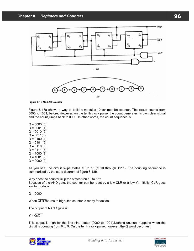
Chapter 8 Registers and Counters 96
Building skills for success
Figure 8-18 Mod-10 Counter
Figure 8-18a shows a way to build a modulus-10 (or mod10) counter. The circuit counts from 0000 to 1001, before. However, on the tenth clock pulse, the count generates its own clear signal and the count jumps back to 0000. In other words, the count sequence is Q = 0000 (0) Q = 0001 (1) Q = 0010 (2) Q = 0011(3) Q = 0100 (4) Q = 0101 (5) Q = 0110 (6) Q = 0111 (7) Q = 1000 (8) Q = 1001 (9) Q = 0000 (0) As you see, the circuit skips states 10 to 15 (1010 through 1111). The counting sequence is summarized by the state diagram of figure 8-18b. Why does the counter skip the states fron 10 to 15? Because of the AND gate, the counter can be reset by a low CLR or a low Y. Initially, CLR goes low to produce Q = 0000 When CLR returns to high, the counter is ready for action. The output of NAND gate is Y = Q3Q1 This output is high for the first nine states (0000 to 1001).Nothing unusual happens when the circuit is counting from 0 to 9. On the tenth clock pulse, however, the Q word becomes

Chapter 8 Registers and Counters 97
Building skills for success
Q = 1010 This means that Q3 and Q1 are high. Almost immediately Y goes low, forcing the counter to reset to Q = 0000 Y then goes high, and the counter is ready to start over. Since it takes 10 clock pulses to reset the counter, the output frequency of the Q3 flip flop is one tenth of the clock frequency. This is why a mod 10 counter is also known as a divide-by-ten circuit. A mod 10 counter like figure 8-18a is often called a decade counter. Because it counts from 0 to 9, it is natural choice in BCD applications like frequency counters, digital voltmeters and electronic wristwatches. To get any other modulus, we can use the same basic idea. For instance, to get a mod-12 counter, we can drive the NAND gate from 0 to 11 (0000 to 1011). On the next clock pulse, Q3 and Q2 are high, which clears the counter. (What is the modulus if Q3 and Q0 drive the NAND gate?)
DOWN CounterDOWN CounterDOWN CounterDOWN Counter
Figure 8-19 Down Counter
All the counters discussed so far have counted upward, toward higher numbers. Figure 8-19 shows a down counter; it counts from 1111 to 0000. Each flip flop toggles when its clock input goes fro 1 to 0. This is equivalent to an un-complemented or complemented outputs going from 1 to 0.For instance, the Q1 flip flop toggles when Q0 goes from 1 to 0; this is equivalent to Q0 gong form 0 to 1. A preset signal generated elsewhere is available in either un-complemented or complemented form; PRE goes to all circuits with an active high preset; PRE goes to all circuits with an active-low preset. Initially, the preset signal PRE goes low in figure 8-19, producing an output word of Q = 1111 (15) When PRE goes high, the action starts. Notice that Q0 toggles once per clock pulse. In the following discussion, a positive toggle means a change from 0 to 1, a negative toggle means a change from 1 to 0.

Chapter 8 Registers and Counters 98
Building skills for success
The first clock pulse produces a negative toggle in Q0, nothing else happens: Q = 11110 (14) The second clock pulse produces a positive toggle which produces a negative toggle n Q1: Q = 1101 (13) On the third clock pulse, Q0 toggles negatively, Q = 1100 (12) On the fourth clock pulse, Q0 toggles positively, and Q2 toggles negatively: Q = 1011 (11) You should have the idea by now. The circuit is counting doen from 15 to 0. when it reaches 0, Q = 0000 On the next clock pulse, all flip flops toggle positively to get Q = 1111 And the cycle repeats.
UPUPUPUP----DOWN counterDOWN counterDOWN counterDOWN counter
Figure 8-20 shows how to build an up-down counter. The flip flops outputs are connected to steering networks. An UP control signal produces either down counting or up counting. If the UP signal is low, Q2, Q1 and Q0 are transmitted to the clock inputs; this results in a down counter. On the other hand, when the UP is high, Q2, Q1 and Q0 drive the clock inputs and the circuit becomes an up counter.

Chapter 8 Registers and Counters 99
Building skills for success
Figure 8-20 Up-Down Counter
Presettable counterPresettable counterPresettable counterPresettable counter
In a presettable counter the count starts at a number greater than zero. Figure 8-21a shows a presettable counter; the count begins with P3P2P1P0, a number between 0000 and 1111.
Figure
Figure 8-21 Presettable Counter
To start the analysis, look at the LOAD control line. When it is low, all NAND gates have high outputs; therefore the preset and clear inputs of all flip flops are inactive. In the case, the circuits

Chapter 8 Registers and Counters 100
Building skills for success
counts upward, as previously described. The data inputs P3 and P0 have no effect because the NAND gates are disabled. When the LOAD line is high, the data inputs and their complements pass through the NAND gates and preset the counter to P3P2P1P0. As an example, suppose the preset input is P3P2P1P0 = 0110 Because of the two left NAND gates, the low P3 produces a high preset and a low clear for the Q3 flip flop; this clears ….

Building skills for success
INTRODUCTION TO DIGITAL CONCEPTS ........................................................1
Section 1.1 Numerical Presentation ............................................................................................................ 1 Analog Representation............................................................................................................................... 1 Digital Representation ............................................................................................................................... 2
Section 1.2 Advantages and Limitations of Digital Techniques................................................................ 3 Advantages ................................................................................................................................................ 3 Limitations................................................................................................................................................. 4
Section 1.3 Number Systems........................................................................................................................ 5 Decimal Number System........................................................................................................................... 5 Binary Number System.............................................................................................................................. 6 Binary Counting ........................................................................................................................................ 7 Octal Number System................................................................................................................................ 7 Hexadecimal Number System ................................................................................................................... 7
Section 1.4 Representing Binary Quantities............................................................................................... 8 Typical Voltage Assignment ..................................................................................................................... 8
Chapter 1 Self Test................................................................................................................................ 9
NUMBER SYSTEM AND CODES......................................................................10
Section 2.1 Binary-To-Decimal Conversion ............................................................................................. 11
Section 2.2 Decimal Number System ........................................................................................................ 11 (A) Repeated Division (Long method)................................................................................................ 11 Decimal to Binary .................................................................................................................................. 12 Decimal to Octal .................................................................................................................................... 13 Decimal to Hexadecimal ...................................................................................................................... 13 (B) Revese of Binary-To-Digital Method (Short method)....................................................................... 13
Section 2.3 Octal Number System............................................................................................................. 15 Octal to Decimal Conversion................................................................................................................... 15 Binary-To-Octal / Octal-To-Binary Conversion...................................................................................... 15 Repeated Division.................................................................................................................................... 16 Octal to Hexadecimal .............................................................................................................................. 16 Short Method: .......................................................................................................................................... 16
Section 2.4 Hexadecimal Number System ................................................................................................ 17 Hexadecimal to Decimal Conversion ...................................................................................................... 17 Repeated Division: Convert decimal to hexadecimal .............................................................................. 17 Binary-To-Hexadecimal /Hexadecimal-To-Binary Conversion .............................................................. 18 Octal-To-Hexadecimal /Hexadecimal-To-Octal Conversion................................................................... 18
Fractional Numbers.................................................................................................................................... 19 Long Method ........................................................................................................................................... 19 Short Method ........................................................................................................................................... 19
BINARY ARITHMETIC .......................................................................................23
Section 3.1 Binary Addition....................................................................................................................... 23
Building skills for success
Section 3.2 Binary Subtraction.................................................................................................................. 23
Section 3.3 Binary Multiplication.............................................................................................................. 24
Section 3.4 Binary Division........................................................................................................................ 24
Section 3.5 Binary Complements .............................................................................................................. 24 1’s Complement....................................................................................................................................... 24 2’s Complement....................................................................................................................................... 25
LOGIC GATES ...................................................................................................26
Section 4.1 Boolean Variables & Truth Tables........................................................................................ 26 Truth Table .............................................................................................................................................. 27 Digital Circuits ........................................................................................................................................ 27 Binary Code............................................................................................................................................. 28
Section 4.2 OR Operation .......................................................................................................................... 28 HOW DOES THE "OR" GATE WORK? ............................................................................................... 29 EXAMPLE OF "OR" GATE OPERATION ........................................................................................... 29
Section 4.3 AND Operation........................................................................................................................ 30 HOW DOES THE "AND" GATE WORK? ............................................................................................ 30 EXAMPLE OF "AND" GATE OPERATION ........................................................................................ 31
Section 4.4 NOT Operation........................................................................................................................ 31 EXAMPLE OF "NOT" GATE OPERATION......................................................................................... 32
Section 4.5 NOR Operation ....................................................................................................................... 32 EXAMPLE OF "NOR" GATE OPERATION......................................................................................... 33
Section 4.6 NAND Operation..................................................................................................................... 34 EXAMPLE OF "NAND" GATE OPERATION ..................................................................................... 35
Section 4.7 XOR Gate................................................................................................................................. 36
Section 4.8 XNOR Gate.............................................................................................................................. 36 Chapter 4 Self Test.............................................................................................................................. 37
BOOLEAN ALGEBRA .......................................................................................40
Section 5.1 Describing Logic Circuits Algebraically ............................................................................... 40 Circuits containing Inverters.................................................................................................................... 41
Section 5.2 Evaluating Logic Circuit Outputs.......................................................................................... 41 Determining Output Level from a Diagram............................................................................................. 42
Section 5.3 Implementing Circuits From Boolean Expression ............................................................... 42
Section 5.4 Boolean Theorems................................................................................................................... 43 Multivariable Theorems........................................................................................................................... 44 Applications of Boolean Algebra ............................................................................................................ 45
Section 5.5 DeMorgan's Theorem ............................................................................................................. 47

Building skills for success
Three Variables DeMorgan's Theorem.................................................................................................... 47 Implications of DeMorgan's Theorem ..................................................................................................... 48
Section 5.6 Universality of NAND & NOR Gates .................................................................................... 49
Section 5.7 Alternate Logic Gate Representations .................................................................................. 50
Section 5.8 Logic Symbol Interpretation .................................................................................................. 51 Combination of Gates .............................................................................................................................. 52
Chapter 5 Self Test.............................................................................................................................. 53
KARNAUGH MAPS............................................................................................58
Section 6.1 Minimization Using Karnaugh Maps .................................................................................... 59
Section 6.2 Grouping Minterms ................................................................................................................ 60
Section 6.3 Incompletely Specified Functions .......................................................................................... 67
Section 6.4 Populating Maps Using 0s Versus 1s ..................................................................................... 69
FLIP FLOPS .......................................................................................................70
Introduction ................................................................................................................................................ 70 Quiz 7.1............................................................................................................................................... 71
Section 7.1 Synchronous and Asynchronous Operation ......................................................................... 71 Quiz 7.2............................................................................................................................................... 72
Section 7.2 Edge-Triggered Flip-flops ...................................................................................................... 73 Edge-triggered S-R flip-flop.................................................................................................................... 73 Edge-triggered J-K flip-flop .................................................................................................................... 74 Edge-triggered D flip-flop ....................................................................................................................... 74
Section 7.3 Summary of the Types of Flip-flop Behaviour ..................................................................... 75 Quiz 7.3............................................................................................................................................... 76
Section 7.4 Pulse-Triggered (Master-Slave) Flip-flops............................................................................ 76
Secion 7.5 Data Lock-Out Flip-flops......................................................................................................... 77
Section 7.6 Operating Characteristics ...................................................................................................... 78
REGISTERS AND COUNTERS .........................................................................79
Section 8.1 Buffer Registers....................................................................................................................... 79 Basic Idea ................................................................................................................................................ 79 Controlled ................................................................................................................................................ 80
Section 8.2 Shift Registers.......................................................................................................................... 82 Shift Left.................................................................................................................................................. 82 Shift Right................................................................................................................................................ 83
Building skills for success
Section 8.3 Controlled Shift Registers ...................................................................................................... 84 SHL Control ............................................................................................................................................ 84
Section 8.4 Ripple Counters....................................................................................................................... 85 The Circuit ............................................................................................................................................... 85 Counting .................................................................................................................................................. 86 Frequency Division.................................................................................................................................. 88 Ripple Counter......................................................................................................................................... 88 Controlled Counter .................................................................................................................................. 88
Section 8.5 Synchronous Counters............................................................................................................ 90 The Circuit ............................................................................................................................................... 90 Controlled Counter .................................................................................................................................. 91
Section 8.6 Ring Counters.......................................................................................................................... 92 The Circuit ............................................................................................................................................... 92 More Bits ................................................................................................................................................. 93 Applications............................................................................................................................................. 93
Section 8.7 Other Counters........................................................................................................................ 95 Mod-10 Counter ...................................................................................................................................... 95 DOWN Counter ....................................................................................................................................... 97 UP-DOWN counter ................................................................................................................................. 98 Presettable counter................................................................................................................................... 99