David C Joy University of Tennessee Oak Ridge National ...
37
The CD-SEM - and beyond David C Joy University of Tennessee Oak Ridge National Laboratory
Transcript of David C Joy University of Tennessee Oak Ridge National ...

The CD-SEM - and beyond
David C JoyUniversity of Tennessee
Oak Ridge National Laboratory

The CD-SEMFor 30 years the performance of electron-optical tools has kept pace with the continuous reduction in feature size but it is no longer possible to anticipate continuous improvements by a factor of two times every three years because the performance is now limited in some fundamental physical areasThe CD-SEM is subject to all the usual constraints that any SEM faces - but operational choices that have to be made can be mutually obstructive …...
Hitachi S-9300 CD SEM

Trends and Consequences
Parameter Trend Drivers Consequences
Beam Energy Lower ChargingBeam Damage
Degraded electron-opticalperformance
Diffraction limitedLow performance electron
sources
Beam Current ConstantTrade-off between
throughput rate, damageand charging
Marginal signal to noise
Spot Size SmallerResolution“Precision”
Lower beam currentDegraded Signal/NoiseDecreased depth of field
Scan Speed HigherThroughput
Charge controlStress on video
componentsPoor linearity
The conflicts
Each of the trends in the table represents a sensible response to a particular problemHowever these parameters interact in a complex wayLowering the beam energy to reduce charging and damage conflicts with the need for ever better imaging resolutionLowering the beam energy reduces the source brightness and reduces beam current - but smaller features and larger wafers demand high currents it throughput rates are to be maintainedHigh scan speeds improve throughput and charging but lead to degraded linearity, and a lower signal to noise ratio

Issues and SolutionsKey Issue Possible Solutions Collateral Damage
ResolutionAberration correction
Higher beam energy
Higher beam current into a smaller probe,but collapse of the Depth of Field
Higher beam current into a smaller probe.Depth of Field about constant
Charge Control
Still lower beam energies
Low vacuum operation
Problem in maintaining opticalperformance
Possible loss in resolution and contrast.Reduction in usable scan speed
Beam induced damageUltra-low energy
High beam energiesElectron-optical performance
Unproven
Contamination(carbon carry-over)
Low vacuum operation
In situ cleaning
Possible loss in resolution and contrast.Reduction in usable scan speed
Damage to resists and oxide layers. Timerequired
3-D information
“Stereo imaging”
Modeling
Requires two exposures.Limited geometries
Needs extensive pre-computation.Accuracy may be limited by charging
Throughput Multiple columns Holographic methods
Complex technology and data handling.Statistical rather than site-specific data
Cost and delay in developing anddelivering new tools
“Common Platform” Needs agreement on basic specificationsand creativity in design

The way forward
There is no simple panacea because every choice carries with it an inescapable side-effect. A piecemeal solution is therefore impossible. Instead it is necessary to look at the tool as a complete systemCan group options together to form scenarios for consideration:the mixture as before (but hopefully better)taking the high energy routelooking for something radically new

Option 1 -The mixture as before
The obvious response is to keep the CD-SEM in the form in which it exists today and try to find some fixes to the problems identified aboveSince the CD-SEM is already operating at very close to its theoretical limits, and the restraints on progress are fundamental in nature, it is clear that this precludes the chance of any one advance resulting in a major step forwardInstead progress must be made simultaneously in several different, key, areas of instrumentation

Key problems -The Electron Source
The brightness of an electron beam varies linearly with the energy with which it hits the target (Langmuir’s Law)– thus a FEG source at 500eV is only about as bright as a tungsten hairpin filament at 20keVMost of the increased brightness obtained from the switch to FEG sources a decade ago is therefore used solely to maintain adequate performance at low energiesTo permit improved operation at lower energies - smaller spots, and higher currents - a much improved source is required. For the 70nm node a factor of 100x over current values is needed
How brightness must be increased to maintain throughput
and give enhanced resolution
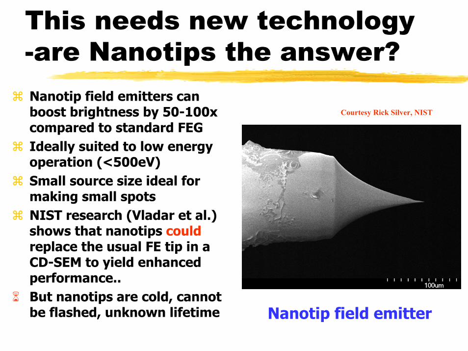
This needs new technology -are Nanotips the answer?Nanotip field emitters can boost brightness by 50-100x compared to standard FEGIdeally suited to low energy operation (<500eV)Small source size ideal for making small spotsNIST research (Vladar et al.) shows that nanotips couldreplace the usual FE tip in a CD-SEM to yield enhanced performance..But nanotips are cold, cannot be flashed, unknown lifetime
Courtesy Rick Silver, NIST
Nanotip field emitter

Comparing Regular and Nano TipsAMAG PolySi sample
Regular FE tip Nano tipS-6000 CD SEM 1989
Courtesy A Vladar and M Postek NIST

Key Problems -Electron Optics performance
Problem -the electron wavelength λ is large at low beam energiesProblem - to minimize chromatic and spherical aberrations the numerical aperture (NA) of the lens has to be kept smallResult - the diffraction disc (=λ/NA) limits the spot sizeFor a CD-SEM lens this gives a probe size of a few nanometers at around 800eV (too big) and currents of a few pA (too small)However the small NA provides a reasonable Depth of Field in the image
Cold FEG
∆E=0.3eV
Size
(Α)

This needs New Technology-Aberration Corrected Lenses
It is now possible to correct lenses for aberration.This enhances performance and allows great flexibility in the design of the lens, stage, and chamber. Note that the optimum NA is higher, so the (diffraction limited) probe size is smaller, and much more beam current is available in the probe (IB~ NA2) for the same gun brightness.
Size
(A)
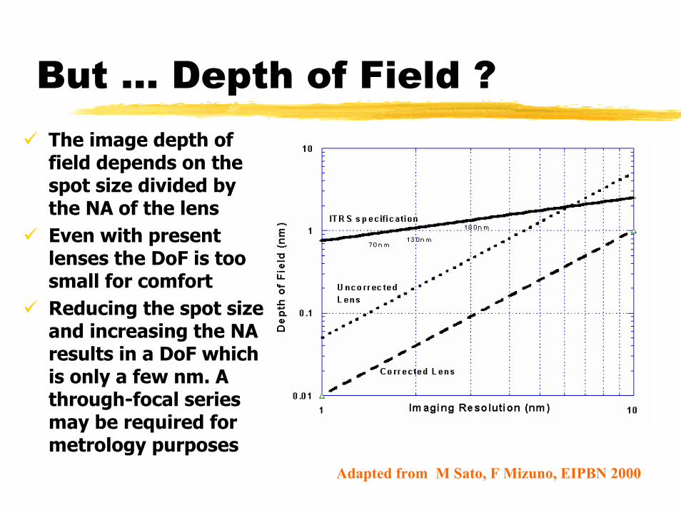
But … Depth of Field ?The image depth of field depends on the spot size divided by the NA of the lensEven with present lenses the DoF is too small for comfortReducing the spot size and increasing the NA results in a DoF which is only a few nm. A through-focal series may be required for metrology purposes
Adapted from M Sato, F Mizuno, EIPBN 2000

Unwanted beam interactions193nm and 157nm resists are highly sensitive to damage from the electron beamThe changes observed are very large compared to desired precision and accuracy
Effect of 0.01µC/cm on protein protoxin
500nm
Shrinkage of 193nm resist with doseSu et al Proc. SPIE 4344, 2001
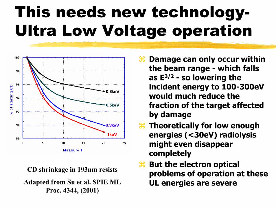
This needs new technology-Ultra Low Voltage operation
Damage can only occur within the beam range - which falls as E3/2 - so lowering the incident energy to 100-300eV would much reduce the fraction of the target affected by damageTheoretically for low enough energies (<30eV) radiolysismight even disappear completelyBut the electron optical problems of operation at these UL energies are severe
CD shrinkage in 193nm resists
Adapted from Su et al. SPIE MLProc. 4344, (2001)

…or Radiation damage is tranmsittedby excitons which can redistribute energy over distances of ~10nmIf they encounter a target of high damage cross-section they transfer their energy to that rather than to the sample of interestSo infiltration of sample with sacrificial species leads to limited protection against radiation damageAnother job for resist chemists? Radiolysis of cell membrane
in frozen glucose (sacrificial component) 200keV beam
Scenario 1 - Conclusions
Follows conventional wisdom and has momentum behind itSignificant amounts of new technology are required. Takes time and moneyThe amount of “upside” performance gain may not be large because too many conflicting factors are involvedFundamental problems (e.g. diffraction) cannot be engineered away
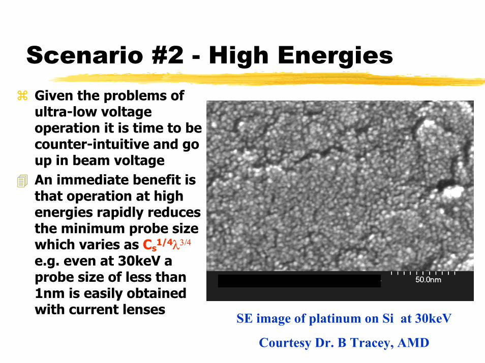
Scenario #2 - High EnergiesGiven the problems of ultra-low voltage operation it is time to be counter-intuitive and go up in beam voltageAn immediate benefit is that operation at high energies rapidly reduces the minimum probe size which varies as Cs
1/4λ3/4e.g. even at 30keV a probe size of less than 1nm is easily obtained with current lenses SE image of platinum on Si at 30keV
Courtesy Dr. B Tracey, AMD
Other advantages of a HV CD-SEM
Significantly higher brightness (30x to 200x that at 1keV) is available from existing sources without the need for new technology. Stable, long-life Schottky emitters can replace cold FEG sources without any loss in resolution due to the increased energy spreadThe column is less susceptible to external EM interferenceContamination and surface coatings have little effect on the imageBecause the electron wavelength is much smaller at higher energies diffraction limiting is reduced and so an acceptable depth of field can be achieved
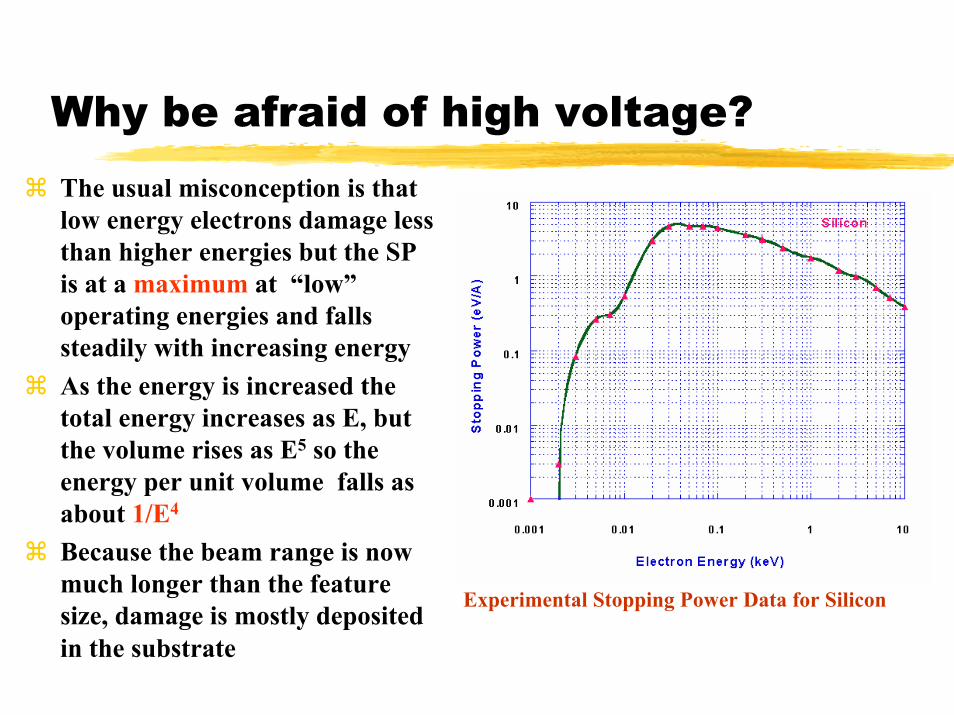
Why be afraid of high voltage?The usual misconception is that low energy electrons damage less than higher energies but the SP is at a maximum at “low” operating energies and falls steadily with increasing energyAs the energy is increased the total energy increases as E, but the volume rises as E5 so the energy per unit volume falls as about 1/E4
Because the beam range is now much longer than the feature size, damage is mostly deposited in the substrate
Experimental Stopping Power Data for Silicon
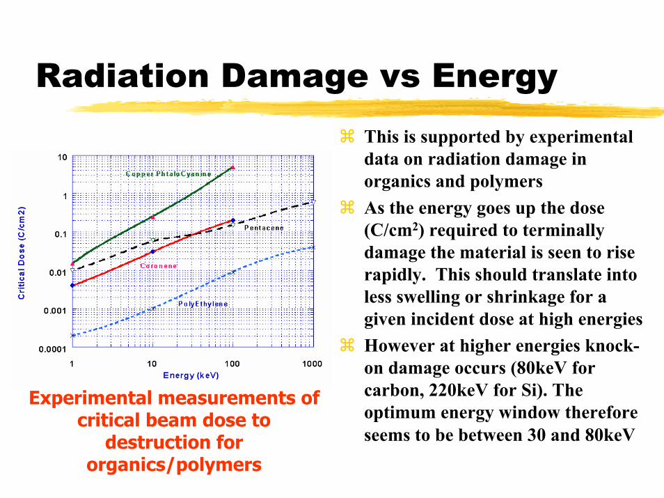
Radiation Damage vs EnergyThis is supported by experimental data on radiation damage in organics and polymersAs the energy goes up the dose (C/cm2) required to terminally damage the material is seen to rise rapidly. This should translate into less swelling or shrinkage for a given incident dose at high energiesHowever at higher energies knock-on damage occurs (80keV for carbon, 220keV for Si). The optimum energy window therefore seems to be between 30 and 80keV
Experimental measurements of critical beam dose to
destruction for organics/polymers
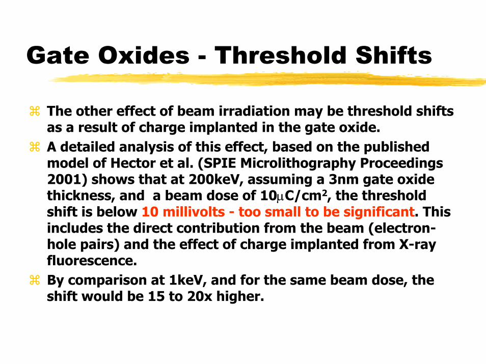
Gate Oxides - Threshold Shifts
The other effect of beam irradiation may be threshold shifts as a result of charge implanted in the gate oxide.A detailed analysis of this effect, based on the published model of Hector et al. (SPIE Microlithography Proceedings 2001) shows that at 200keV, assuming a 3nm gate oxide thickness, and a beam dose of 10µC/cm2, the threshold shift is below 10 millivolts - too small to be significant. This includes the direct contribution from the beam (electron-hole pairs) and the effect of charge implanted from X-ray fluorescence.By comparison at 1keV, and for the same beam dose, the shift would be 15 to 20x higher.
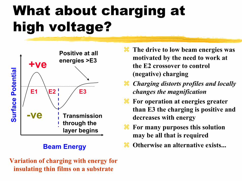
What about charging at high voltage?
The drive to low beam energies was motivated by the need to work at the E2 crossover to control (negative) charging Charging distorts profiles and locally changes the magnificationFor operation at energies greater than E3 the charging is positive and decreases with energyFor many purposes this solution may be all that is requiredOtherwise an alternative exists...Beam Energy
Surf
ace
Pote
ntia
l
E1 E2 E3
-ve Transmission through the layer begins
Variation of charging with energy for insulating thin films on a substrate
Positive at all energies >E3+ve

Charging in a gas
Surrounding the sample with a low pressure atmosphere of gas allows the charging to be controlled in a simple wayThis action is self controllingThe gas does not limit high resolution performance
Experimental charging data for a EUV Cr on Glass mask. Air environment, 200pA current
500nm20keV image at 400Pa (3T) of air
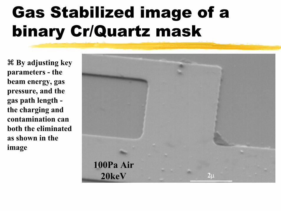
Gas Stabilized image of a binary Cr/Quartz mask
2µ100Pa Air
20keV
By adjusting key parameters - the beam energy, gas pressure, and the gas path length -the charging and contamination can both the eliminated as shown in the image
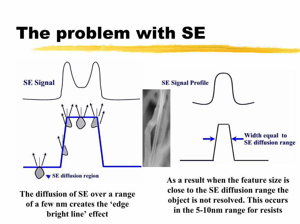
The problem with SE
As a result when the feature size is close to the SE diffusion range the object is not resolved. This occurs
in the 5-10nm range for resists
The diffusion of SE over a range of a few nm creates the ‘edge
bright line’ effect
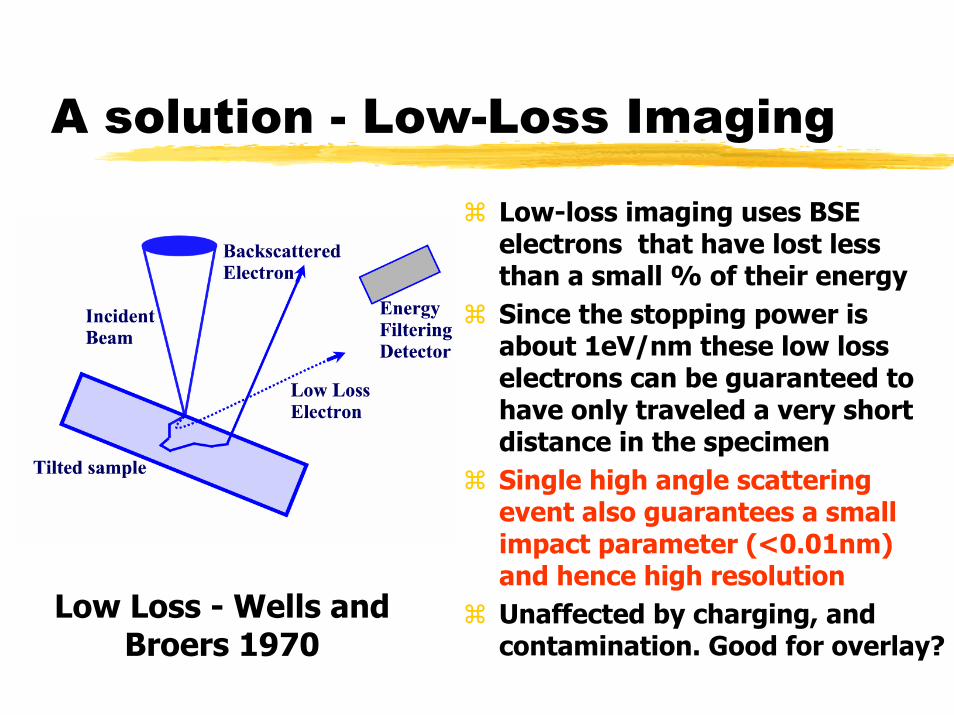
A solution - Low-Loss Imaging
Low-loss imaging uses BSE electrons that have lost less than a small % of their energySince the stopping power is about 1eV/nm these low loss electrons can be guaranteed to have only traveled a very short distance in the specimenSingle high angle scattering event also guarantees a small impact parameter (<0.01nm) and hence high resolutionUnaffected by charging, and contamination. Good for overlay?
Low Loss - Wells and Broers 1970
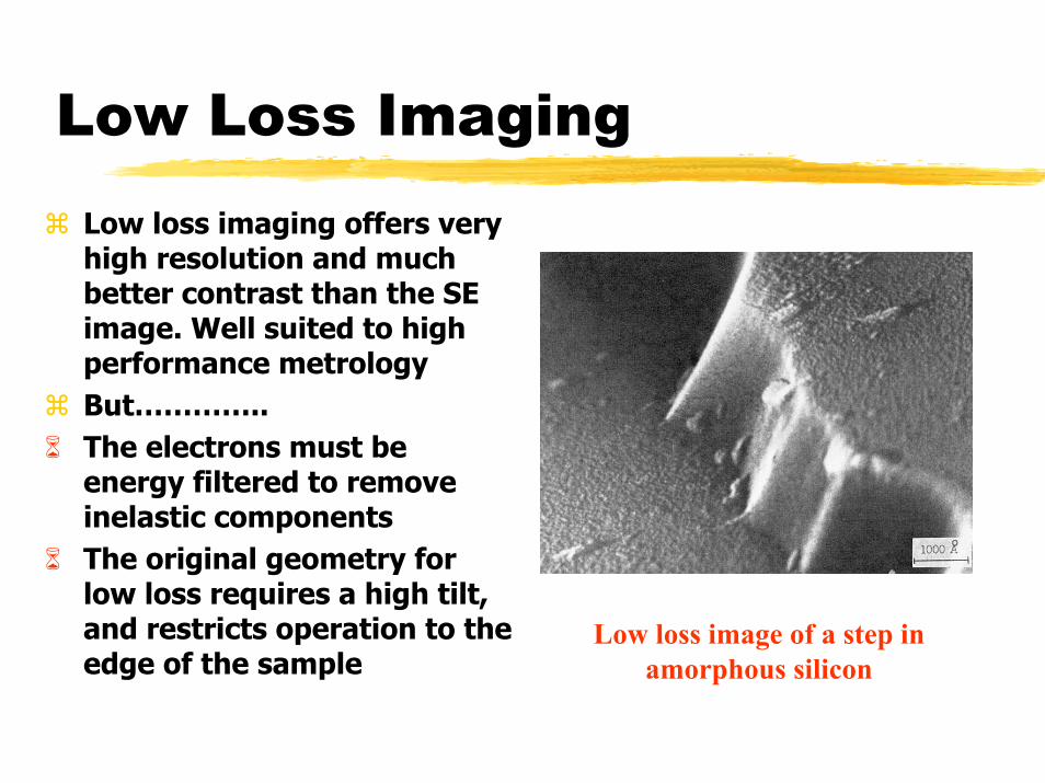
Low Loss ImagingLow loss imaging offers very high resolution and much better contrast than the SE image. Well suited to high performance metrologyBut…………..The electrons must be energy filtered to remove inelastic componentsThe original geometry for low loss requires a high tilt, and restricts operation to the edge of the sample
Low loss image of a step in amorphous silicon
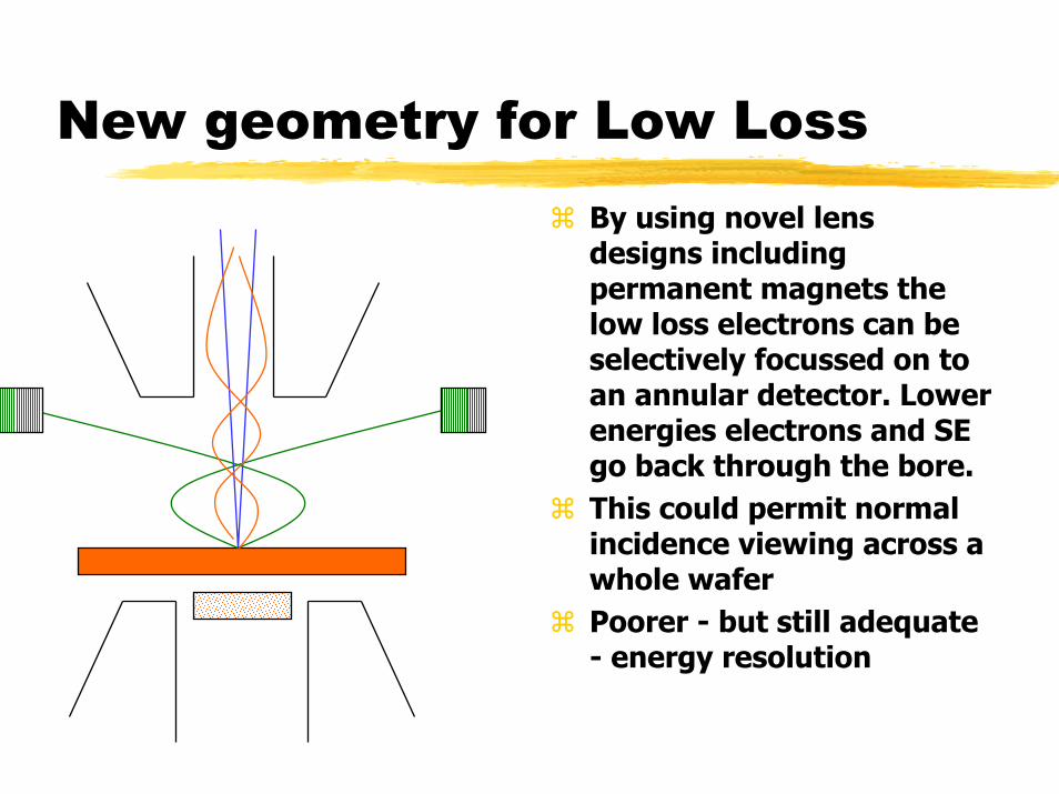
New geometry for Low LossBy using novel lens designs including permanent magnets the low loss electrons can be selectively focussed on to an annular detector. Lower energies electrons and SE go back through the bore.This could permit normal incidence viewing across a whole waferPoorer - but still adequate - energy resolution
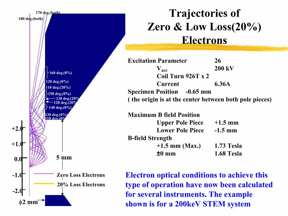
5 mm
φ2 mm
180 deg.(both)170 deg.(both)
160 deg.(0%)
150 deg.(0%)
140 deg.(0%)
130 deg.(0%)
120 deg.(0%)
110 deg.(0%)
110 deg.(20%)
120 deg.(20%)130 deg.(20%)
Zero Loss Electrons
20% Loss Electrons
0.0
-1.0
-2.0
+1.0
+2.0
Electron optical conditions to achieve this type of operation have now been calculated for several instruments. The example shown is for a 200keV STEM system
Trajectories of Zero & Low Loss(20%)
Electrons
Excitation Parameter 26Vacc 200 kVCoil Turn 926T x 2Current 6.36A
Specimen Position -0.65 mm( the origin is at the center between both pole pieces)
Maximum B field PositionUpper Pole Piece +1.5 mmLower Pole Piece -1.5 mm
B-field Strength+1.5 mm (Max.) 1.73 Tesla±0 mm 1.68 Tesla

Low Loss operation
The predicted conditions for the new Low Loss geometry have been demonstrated to produce good quality imagesThe LL signal to noise ratio is lower than desirable because of limitations in the detectorThe comparative images show that the familiar artifacts of SE imaging (the edge brightness effects, charging) are absent and edge definition is enhanced
Low Loss
SE
0.5µ
A resist structure recorded in Low Loss mode using the new geometry, and the corresponding SE image. 5keV operation, Hitachi S4300SE
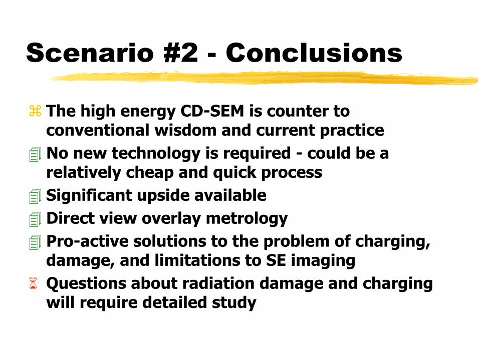
Scenario #2 - Conclusions
The high energy CD-SEM is counter to conventional wisdom and current practiceNo new technology is required - could be a relatively cheap and quick processSignificant upside availableDirect view overlay metrologyPro-active solutions to the problem of charging, damage, and limitations to SE imagingQuestions about radiation damage and charging will require detailed study
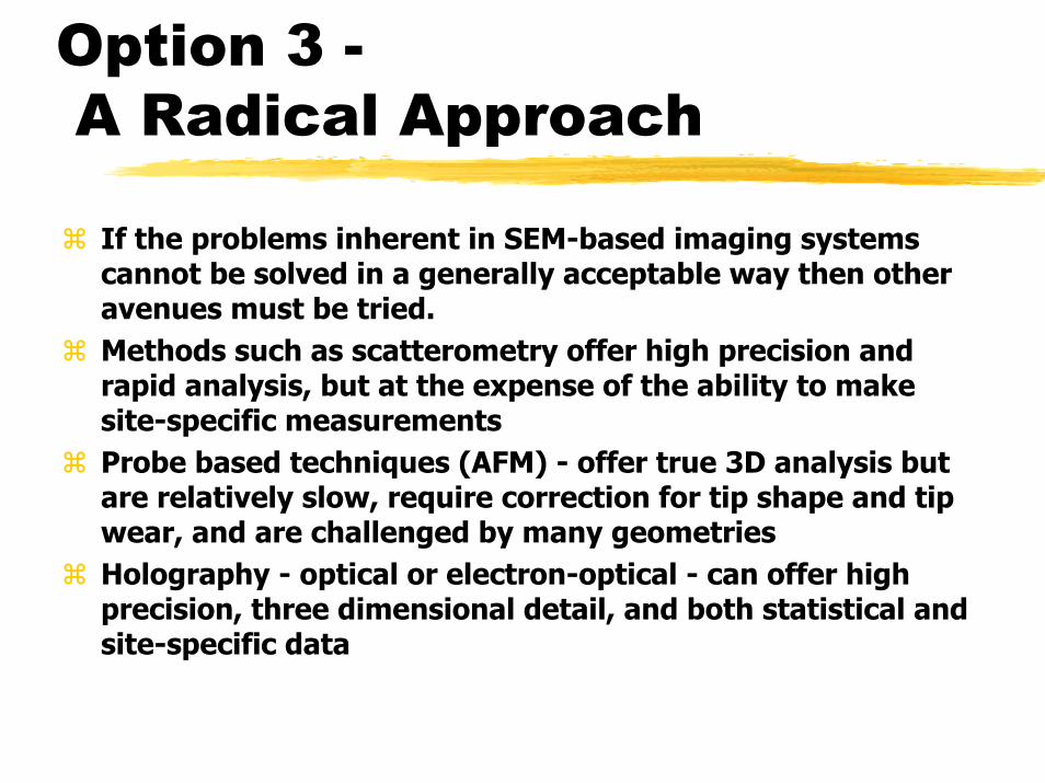
Option 3 -A Radical Approach
If the problems inherent in SEM-based imaging systems cannot be solved in a generally acceptable way then other avenues must be tried.Methods such as scatterometry offer high precision and rapid analysis, but at the expense of the ability to make site-specific measurementsProbe based techniques (AFM) - offer true 3D analysis but are relatively slow, require correction for tip shape and tip wear, and are challenged by many geometriesHolography - optical or electron-optical - can offer high precision, three dimensional detail, and both statistical and site-specific data
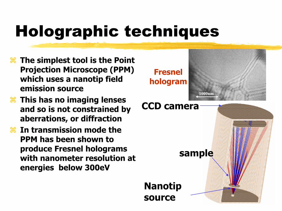
Holographic techniques
sample
CCD camera
Fresnel hologram
The simplest tool is the Point Projection Microscope (PPM) which uses a nanotip field emission sourceThis has no imaging lenses and so is not constrained by aberrations, or diffractionIn transmission mode the PPM has been shown to produce Fresnel holograms with nanometer resolution at energies below 300eV
Nanotip source

New PPM Reflection Geometry
The system has now been configured to produce vertical incidence and reflectionThe nanotip emitter no longer uses the sample as an anode. Instead a self - contained nanogun has been developedThe sample potential can now be varied around zero to provide a variety of imaging modes including ‘mirror’ operation
screen
nanotip
“nanogun”
crossover -point source
bias
reflected rays
X
Y
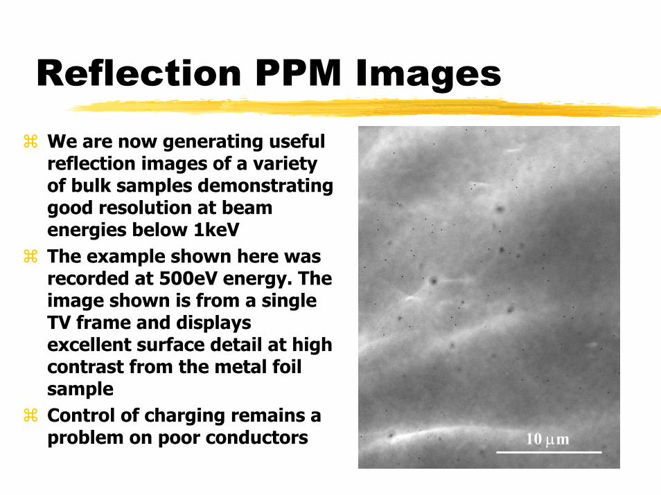
Reflection PPM Images
10 µm
We are now generating useful reflection images of a variety of bulk samples demonstrating good resolution at beam energies below 1keVThe example shown here was recorded at 500eV energy. The image shown is from a single TV frame and displays excellent surface detail at high contrast from the metal foil sampleControl of charging remains a problem on poor conductors
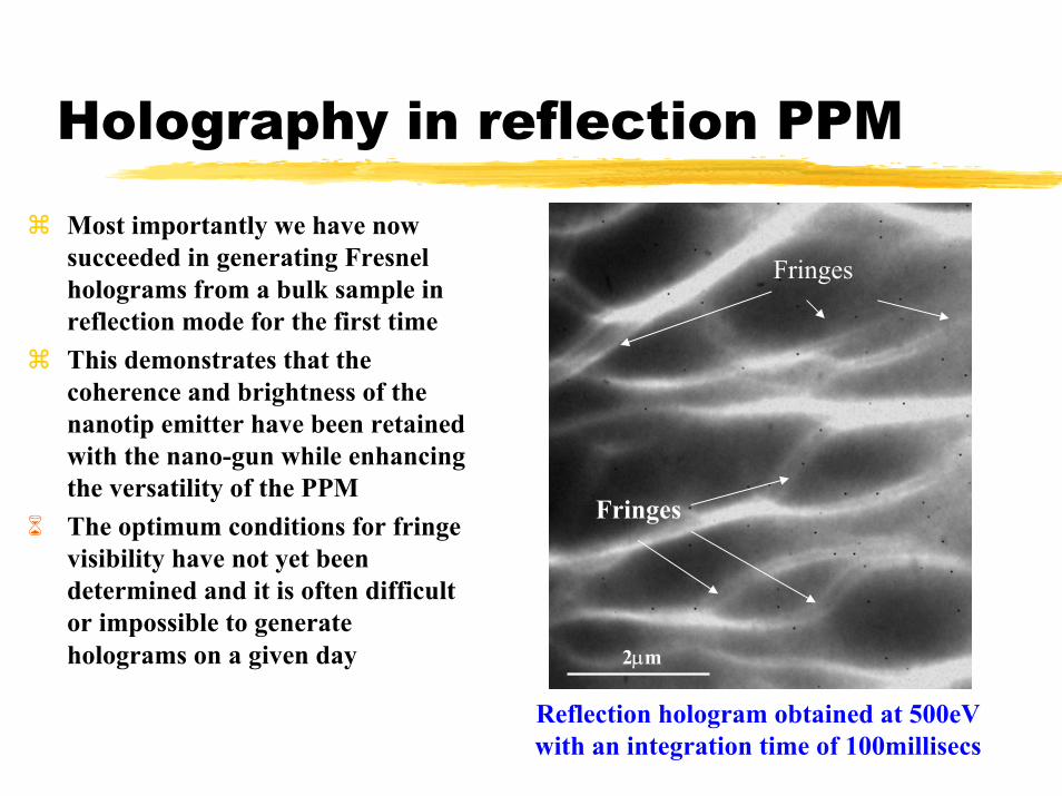
Holography in reflection PPM
Fringes
Fringes
2µm
Most importantly we have now succeeded in generating Fresnelholograms from a bulk sample in reflection mode for the first timeThis demonstrates that the coherence and brightness of the nanotip emitter have been retained with the nano-gun while enhancing the versatility of the PPMThe optimum conditions for fringe visibility have not yet been determined and it is often difficult or impossible to generate holograms on a given day
Reflection hologram obtained at 500eV with an integration time of 100millisecs