CHAPTER 4 - CMOS...
32
Current Mirrors (5/11/00) Page 1 ECE 4430 - Analog Integrated Circuits and Systems P.E. Allen, 2000 CURRENT MIRRORS INTRODUCTION Objective The objective of this presentation is: 1.) Introduce and characterize the current mirrors 2.) Show how to improve the performance of the current mirrors 3.) Demonstrate the design of current mirrors Outline • Simple MOS current mirrors • Simple BJT current mirrors • Cascode current mirrors • Wilson current mirrors • Regulated-cascode current mirrors • Summary
Transcript of CHAPTER 4 - CMOS...

Current Mirrors (5/11/00) Page 1
ECE 4430 - Analog Integrated Circuits and Systems P.E. Allen, 2000
CURRENT MIRRORS INTRODUCTION
Objective The objective of this presentation is: 1.) Introduce and characterize the current mirrors 2.) Show how to improve the performance of the current mirrors 3.) Demonstrate the design of current mirrors Outline • Simple MOS current mirrors • Simple BJT current mirrors • Cascode current mirrors • Wilson current mirrors • Regulated-cascode current mirrors • Summary

Current Mirrors (5/11/00) Page 2
ECE 4430 - Analog Integrated Circuits and Systems P.E. Allen, 2000
SIMPLE MOS CURRENT MIRRORS
Characterization of Current Mirrors A current mirror is basically nothing more than a current amplifier. The ideal characteristics of a current amplifier are: • Output current linearly related to the input current, iout = Aiiin
• Input resistance is zero • Output resistance is infinity In addition, we have the characteristic VMIN which applies not only to the output but also the input.
• VMIN(in) is the range of input voltage over which the input resistance is not small
• VMIN(out) is the range of the output voltage over which the output resistance is not large
Graphically:
CurrentMirror
+
-vin
iin+
-vout
iout
vin
iin
VMIN (in)
Slope= 1/Rin
iin vout
iout
VMIN (out)
Slope = 1/Rout
iout
1Ai
Fig. 4.4-1Input Characteristics Transfer Characteristics Output Characteristics
Therefore, we will focus on Rout, Rin, VMIN(out), VMIN(in), and Ai to characterize the current mirror.

Current Mirrors (5/11/00) Page 3
ECE 4430 - Analog Integrated Circuits and Systems P.E. Allen, 2000
Simple MOS Current Mirror
M1 M2
iI iO
+
-
vDS1
+
-
vDS2
Fig. 4.4-2
+-vGS-
Assume that vDS2 > vGS - VT2, then
iOiI
=
L1W2
W1L2
VGS-VT2
VGS-VT1
2
1 + λvDS2
1 + λvDS1
K2’
K1’
If the transistors are matched, then K1’ = K2’ and VT1 = VT2 to give,
iOiI
=
L1W2
W1L2
1 + λvDS2
1 + λvDS1
If vDS1 = vDS2, then
iOiI
=
L1W2
W1L2
Therefore the sources of error are 1.) vDS1≠ vDS2 and 2.) M1 and M2 are not matched.

Current Mirrors (5/11/00) Page 4
ECE 4430 - Analog Integrated Circuits and Systems P.E. Allen, 2000
Influence of the Channel Modulation Parameter, λλλλ If the transistors are matched and the W/L ratios are equal, then
iOiI
= 1 + λvDS21 + λvDS1
assuming that the channel modulation parameter is the same for both transistors (L1 = L2).
Ratio error (%) versus drain voltage difference:
4.0
8.0
5.0
6.0
7.0
0.0
3.0
2.0
1.0
0.0 5.0 vDS2 - vDS1 (volts)
λ = 0.01
1.0 2.0
λ = 0.015
λ = 0.02
Ratio Error vDS2 - vDS1 (volts)
v DS2
v DS1
1 11
100
+ +−
×λ λ
%R
atio
Err
or
vDS1 = 2.0 volt
Fig. 4.4-33.0 4.0
Note that one could use this effect to measure λ. Measure VDS1,VDS2, iI and iO and solve the above equation for the channel modulation parameter, λ.

Current Mirrors (5/11/00) Page 5
ECE 4430 - Analog Integrated Circuits and Systems P.E. Allen, 2000
Influence of Mismatched Transistors
Assume that vDS1 = vDS2 and that K1’ ≠ K2’ and VT1 ≠ VT2. Therefore we have
iOiI
= K2’(vGS - VT2)2
K1’(vGS - VT1)2
How do you analyze the mismatch? Use plus and minus worst case approach. Define
∆K’ = K’2 - K’1 K’ = 0.5(K2’ + K1’ ) ∆VT = VT2 - VT1 and VT = 0.5(VT1+VT2). ∴ K1’ = K’ - 0.5∆K’ K2’ = K’ + 0.5∆K’ VT1 = VT -0.5∆VT and VT2 = VT+0.5∆VT
Substituting these terms into the above equation gives,
iOiI
= (K’+0.5∆K’)(vGS - VT - 0.5∆VT )2
(K’-0.5∆K’)(vGS - VT + 0.5∆VT)2 =
1 + ∆K’2K’
1 - ∆VT
2(vGS-VT)2
1 - ∆K’2K’
1 + ∆VT
2(vGS-VT)2
Assuming that the terms added to or subtracted from “1” are smaller than unity gives
iOiI
♠
1 + ∆K’2K’
1 + ∆K’2K’
1 - ∆VT
2(vGS-VT)2
1 - ∆VT
2(vGS-VT)2 Uses the approximation 1/(1+ε) ≈ 1-ε
Retaining only first order products gives
iOiI
♠ 1 + ∆K’K’ -
2∆VT(vGS-VT)
Assume ∆K’/K’ = ±5% and ∆VT/(vGS-VT) = ±10%.
∴ iO/iI ≈ 1 ± 0.05 ±(-0.20) = 1 ± (0.25) ⇒ ±15% error in gain if tolerances are correlated.
Current Mirrors (5/11/00) Page 6
ECE 4430 - Analog Integrated Circuits and Systems P.E. Allen, 2000
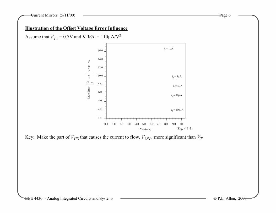
Illustration of the Offset Voltage Error Influence
Assume that VT1 = 0.7V and K’W/L = 110µA/V2.
8.0
16.0
10.0
12.0
14.0
0.0
6.0
4.0
2.0
0.0 10
∆VT (mV)
1.0 2.0
i O i i
100
×%
Rat
io E
rror
1−
iI = 1µA
3.0 4.0 5.0 6.0 7.0 8.0 9.0
iI = 3µA
iI = 5µA
iI = 10µA
iI = 100µA
Fig. 4.4-4 Key: Make the part of VGS that causes the current to flow, VON, more significant than VT.

Current Mirrors (5/11/00) Page 7
ECE 4430 - Analog Integrated Circuits and Systems P.E. Allen, 2000
Influence of Error in Aspect Ratio of the Transistors Example 1 - Aspect Ratio Errors in Current Mirrors
Figure 4.4-4 shows the layout of a one-to-four current amplifier. Assume that the lengths are identical (L1 = L2) and find the ratio error if W1 = 5 ± 0.1 µm. The actual widths of the two transistors are
W1 = 5 ± 0.1 µm andW2 = 20 ± 0.1 µm
Solution We note that the tolerance is not multiplied by the nominal gain factor of 4. The ratio of W2 to W1 and consequently the gain of the current amplifier is
iOiI
= W2W1
= 20 ± 0.15 ± 0.1 = 4
1 ±
0.120
1 ± 0.15
♠ 4
1 ± 0.120
1 -±0.1
5 ♠ 4
1 ± 0.120 -
±0.420 = 4 - (±0.06)
where we have assumed that the variations would both have the same sign (correlated). It is seen that this ratio error is 1.5% of the desired current ratio or gain.
iO
M1 M2
+
-
+
-
+
-
VDS1VDS2
iI
VGS����������
M1M2iO iI
GND
Fig. 4.4-5

Current Mirrors (5/11/00) Page 8
ECE 4430 - Analog Integrated Circuits and Systems P.E. Allen, 2000
Influence of Error in Aspect Ratio of the Transistors-Continued Example 2 - Reduction of the Aspect Ratio Errors in Current Mirrors Use the layout technique illustrated in Fig. 4.4-5 and calculate the ratio error of a current amplifier having the specifications of the previous example. Solutions The actual widths of M1 and M2 are
W1 = 5 ± 0.1 µm and W2 = 4(5 ± 0.1) µm
The ratio of W2 to W1 and consequently the current gain is given below and is for all practical purposes independent of layout error.
iOiI
= 4(5 ± 0.1)
5 ± 0.1 = 4
��������
��������
��������
����
����M1M2bM2a M2dM2c iO
M1 M2
iI
iI
GND
GND
iO
Fig. 4.4-6

Current Mirrors (5/11/00) Page 9
ECE 4430 - Analog Integrated Circuits and Systems P.E. Allen, 2000
Summary of the Simple MOS Current Mirror/Amplifier • Minimum input voltage is VMIN(in) = VT+VON
Okay, but could be reduced to VON.
Principle:
M1M2
VTiI iO
VT+VON+-
+
-VON
M1 M2VT
Fig. 4.4-7
iI iO
VT+VON
+
-
+
-
VON
Ib
IbIb
VDD
Ib
M3 M4
M5 M6 M7
Will deal with later in low voltage op amps. • Minimum output voltage is VMIN(out) = VON
• Output resistance is Rout = 1
λID
• Input resistance is Rin ≈ 1
gm
• Current gain accuracy is poor because vDS1 ≠ vDS2

Current Mirrors (5/11/00) Page 10
ECE 4430 - Analog Integrated Circuits and Systems P.E. Allen, 2000
SIMPLE BJT CURRENT MIRRORS Characterization of a Simple BJT Current Mirror
vBE
CM10
Q1 Q2
iC1
iC2 = i2
iB1 iB2
i1
+
-
Rout = ro2 = VA2IC2
Rin ≈ 1
gm1 =
VtIC1
VMIN(out) = vCE(sat) ≈ 0.2V
VMIN(in) = VBE ≈ 0.6 to 0.7V
and
Ai = Is2Is1
if the transistors are matched and β = ∞.

Current Mirrors (5/11/00) Page 11
ECE 4430 - Analog Integrated Circuits and Systems P.E. Allen, 2000
Simple BJT Current Mirror Matching Circuit:
i1 = iC1 + iB1 + iB2 = iE1 + iB2 = iC1αF1
+ iB2
iC1 =
1 +
vCE1VA1
Is1 exp(vBE/Vt)
and
iC2 = i2 =
1 +
vCE2VA2
Is2 exp(vBE/Vt)
Now,
i1 =
1 +
vCE1VA1
Is1
αF1 exp(vBE/Vt) + iB2 and iB2 =
iC2βF2
= i2
βF2 =
1-αF2
αF2
1+
v2VA2
Is2 exp(vBE/Vt)
∴ i1 =
1 +
v1VA1
Is1
αF1 +
1-αF2
αF2
1+
v2VA2
Is2 exp(vBE/Vt)
Finally,
i2i1
=
1+
v2VA2
1 +
v1VA1
Is1
αF1 +
1-αF2
αF2
1+
v2VA2
Is2
vBE
CM11
Q1 Q2
iC1
iC2 = i2
iB1 iB2
i1
+
-
+
-
vCE1 = v1vCE2 = v2
+
-

Current Mirrors (5/11/00) Page 12
ECE 4430 - Analog Integrated Circuits and Systems P.E. Allen, 2000
Simple BJT Current Mirror Matching - Continued
Using a Taylor series expansion and ignoring the second-order terms, we have
i2i1 ≈
IS2
1 + v1
VA1 -
v2VA2
Is1
αF1 +
(1- αF2)
αF2Is2
For large βF (αF ≈ 1):
i2i1 ≅
Is2
1 + v1
VA1 -
v2VA2
Is1
Again using Taylor-series expansion:
i2i1 ≈
Is2
Is1
1 - v1
VA1 +
v2VA2
Let ∆Is = Is2 - Is1 and Is ≈ Is1 ≈ Is2
i2i1 ≈
1 + ∆IsIs
1 - v1
VA1 +
v2VA2
For v1 = VBE = 0.7V, v2 = 5V, ∆IsIs
= 0.02, VA = 50
i2i1 ≈ 1.11 > 11% error due primarily to mismatch in Rout (v1 and v2)

Current Mirrors (5/11/00) Page 13
ECE 4430 - Analog Integrated Circuits and Systems P.E. Allen, 2000
Geometrical Influence on BJT Matching
If everything is ideal (βF = ∞ and VCE1 = VCE2), the matching of the currents is determined by the matching of the saturation currents, Is, which is given as
Is = qni2D n
NAWB(VCB) AE = qni2D n
QB(VCB) AE
Therefore, the transistor matching directly depends on how well the emitter areas are matched. If a current gain greater than 1 is required, the emitter areas should be implemented as follows:
CM19
C1
C2
E2E1
B2
B1
Metal 2
Metal 1
Current gain of the above structure is 1.5.
CM18
Emitter AreaCollectorContact Base
Contact
Emitter Contact

Current Mirrors (5/11/00) Page 14
ECE 4430 - Analog Integrated Circuits and Systems P.E. Allen, 2000
Rules for Matching of NPN BJT Transistors† 1. Use identical emitter geometries. 2. The emitter diameter should equal 2-10 times the minimum allowed diameter. 3. Maximize the emitter area-to-periphery ratio (circle the best, square okay). 4. Place matched transistors in close proximity 5. Keep the layout of matched transistors as compact as possible. 6. Construct ratioed pairs and quads using even integer ratios between 4:1 and 16:1 7. Place matched transistors far away from power devices. 8. Place matched transistor in low-stress areas (thermal and physical). 9. Place moderately or precisely matched transistors on axes of symmetry of the die. 10. Do not allow the buried layer shadow to intersect matched emitters (must overlay the emitter area). 11. Place emitters far enough apart to avoid interactions. 12. Increase the base overlap of moderately or precisely matched emitters. 13. Operate matched transistors on the flat portion of the beta curve. 14. The contact geometry should match the emitter geometry (circular contact for circular structure, square contact
for square structure, etc.). 15. Consider using emitter degeneration.
† Alan Hastings, “The Art of Analog Layout”, Chapter 9, 1998 (Unpublished text, [email protected])

Current Mirrors (5/11/00) Page 15
ECE 4430 - Analog Integrated Circuits and Systems P.E. Allen, 2000
Rules for Matching Lateral PNP Transistors
1. Use identical emitter and collector geometries. 2. Use minimum-size emitters for matched transistors. 3. Field plate the base region of mateched lateral PNP transistors. 4. Split-collector lateral PNP transistors can achieve moderate matching. 5. Place matched transistors in close proximity. 6. If possible, avoid constructing VPTAT circuits from ratioed lateral PNP transistors. 7. Place matched transistors far away from power devices. 8. Place matched transistor in low-stress areas (thermal and physical). 9. Place moderately or precisely matched transistors on axes of symmetry of the die. 10. Do not allow the buried layer shadow to intersect matched emitters (must overlay the emitter area). 11. Operate matched lateral PNP transistors near peak beta. 12. The contact geometry should match the emitter geometry (circular contact for circular structure, square contact
for square structure, etc.). 13. Consider using emitter degeneration.

Current Mirrors (5/11/00) Page 16
ECE 4430 - Analog Integrated Circuits and Systems P.E. Allen, 2000
Simple BJT Current Mirror for Finite ββββ Circuit:
If the transistors are matched and vCE1 = vCE2, then iC1 = iC2 but
iC1 = i1 - 2iB = i1
1+ 2β
∴ Ai = i2i1
= 1
1+2β
If βF is small then appreciable error is introduced into the current gain.
Solutions to this problem:
VCC
CM12
Q1 Q2
iC1 iC2Q3
VCC
Q1 Q2
iC1 iC2Q3or
vBE
CM10
Q1 Q2
iC1
iC2 = i2
iB1 iB2
i1
+
-

Current Mirrors (5/11/00) Page 17
ECE 4430 - Analog Integrated Circuits and Systems P.E. Allen, 2000
Base-Current Cancellation In a BiCMOS process, base current cancellation is possible and using the following technique.
VDD
CM13
Q1
Q2
M1 M2
M3 M4
IB1
IB2
IB2I ≈ 0
If Q1 and Q2 are matched, then IC1 ≈ IC2 and IB1 ≈ IB2.
The cascode current mirror is used to make sure that IB1 = IB2.

Current Mirrors (5/11/00) Page 18
ECE 4430 - Analog Integrated Circuits and Systems P.E. Allen, 2000
CASCODE CURRENT MIRRORS MOS Cascode Current Mirror Improving the output resistance:
iI iO
M3
M1 M2
M4
Fig. 4.4-8
gm3v3 rds3
+
-
v3
gm1v1 rds1
+
-
v1
D3=G3=G4
S3=G2
D1=G1
S1
gm4vgs4rds4
rds2
D4
S4
D2
S2gm2vgs2
+
-
viniin
+
-
vout iout
• Rout:
vout = rds4(iout-gm4vgs4) + rds2(iout-gm2vgs2)
But, iin = 0 so that v1 = v3 = 0 ⇒ vgs4 = -vs4 = -ioutrds2 and vgs2 = 0
∴ vout = iout[rds4 + rds2 + gm4rds2rds4] ≈ rds2gm4rds4
• Rin:
Rin = 1
gm3 ||rds3 +
1gm1
||rds1 ≈ 1
gm1 +
1gm3
≈ 2
gm
• VMIN(out) = VT + 2VON
• VMIN(in) = 2(VT +VON)
• Current gain match: Excellent since vDS1 = vDS2

Current Mirrors (5/11/00) Page 19
ECE 4430 - Analog Integrated Circuits and Systems P.E. Allen, 2000
Large Output Swing Cascode Current Mirror
M2
M1M3
1/4
M4
VDD
IREF IREF iO
M5
Fig. 4.4-9
iI
1/1
1/1
1/1
1/1
gm5vgs5rds5
gm3vgs3 rds1
+
-
vs5
D5=G3
D3=S5
S3=G5
+
-
viniin
= gm3vin
• Rout ≈ gm2rds2rds1 • Rin = ? vin = rds5(iin - gm5vgs5) + vs5 = rds5(iin + gm5vs5) + vs5 = rds5iin + (1+gm5rds5)vs5
But, vs5 = rds3(iin - gm3vin)
∴ vin = rds5iin + (1+gm5rds5)rds3iin - gm3rds3(1+gm5rds5)vin
Rin = viniin
= rds5 + rds3 + rds3gm5rds5
gm3rds3(1+gm5rds5) ♠ 1
gm3
• VMIN(out) = 2VON
• VMIN(in) = VT + VON
• Current gain is excellent because vDS1 = vDS3.

Current Mirrors (5/11/00) Page 20
ECE 4430 - Analog Integrated Circuits and Systems P.E. Allen, 2000
Self-Biased Cascode Current Mirror VDD VDD
I1 I2iin iout
R
M1 M2
M3 M4
gm3vgs3
rds3
R
gm1vgs1 rds1
+
-
vin
+
-
v2v1
+
-
+
-
vin
Small-signal model to calculate Rin.Self-biased, cascode current mirror Fig. 4.4-10
iin
• Rin = ? vin = iinR + rds3(iin-gm3vgs3) + rds1(iin-gm1vgs1)
But, vgs1 = vin - iinR and vgs3 = vin - rds1(iin-gm1vgs1) = vin - rds1iin + gm1rds1(vin-iinR)
∴ vin = iinR + rds3iin - gm3rds3[vin - rds1iin + gm1rds1(vin-iinR)] + rds1[iin - gm1(vin+iinR)]
vin[1 + gm3rds3 + gm1rds1gm3rds3 + gm1rds1] = iin[R + rds1 + rds3 + gm3rds3rds1 + gm1rds1gm3rds3R]
Rin = R + rds1 + rds3 + gm3rds3rds1 + gm1rds1gm3rds3R
1 + gm3rds3 + gm1rds1gm3rds3 + gm1rds1 ♠
1gm1
+ R
• Rout ≈ gm4rds4rds2
• VMIN(in) = VT + 2VON •VMIN(out) = 2VON • Current gain matching is excellent

Current Mirrors (5/11/00) Page 21
ECE 4430 - Analog Integrated Circuits and Systems P.E. Allen, 2000
BJT Cascode Current Mirror
CM14
Q1 Q2
i1 i2
Q3 Q4
+VBE1-
+VBE3-
+VBE4-
+
-
VCE1
+
-
VCE4
Advantages:
Because VCE1= VCE2, this mirror will have very good matching if βF is very large.
Output resistance large because of cascoded output (Rout ≈ βF4ro2)
Disadvantages: VMIN (out) = VBE1 + vCE4(sat)
VMIN (in) = VBE1 + VBE3 = 2VBE

Current Mirrors (5/11/00) Page 22
ECE 4430 - Analog Integrated Circuits and Systems P.E. Allen, 2000
Improving the Matching of the BJT Cascode Current Mirror VDD
CM15
Q4
Q5
X2
IB
IB
2IB2
I ≈ 0
Q1 Q2
iIN iOUTX2
Q3
IBIB
VDD
Q4
M5
IB2IB
I ≈ 0
Q1 Q2
iIN
iOUT
Q3
IBIB
IB
2IB
Achieves the desired base current
cancellation However, there are three transistors stacked at the output which will cause a large VMIN
Achieves the desired base current cancellation using only two stacked transistors VMIN = VBE + vCE(sat)

Current Mirrors (5/11/00) Page 23
ECE 4430 - Analog Integrated Circuits and Systems P.E. Allen, 2000
Improving VMIN of the BJT Cascode Current Mirror
Use the “trick” of freeing the voltage at the bases of the cascode transistors to get,
CM16
Q1 Q2
i1 i2
Q3 Q4
+VBE-
+VBE-
+VBE-
+
-
vCE(sat)
+
-
VCE
VBE +vCE(sat)
vCE(sat)+
-
+
-VBE
Advantages: VMIN(out) = 2vCE(sat)
Rout ≈ βFro
VMIN(in) = VBE (lowest possible without using extreme methods) Disadvantages:
Screwed up the current mismatch. Okay if βF is large or you can use another transistor but VMIN(in) will increase.
Requires a battery of VBE +vCE(sat)

Current Mirrors (5/11/00) Page 24
ECE 4430 - Analog Integrated Circuits and Systems P.E. Allen, 2000
Self-Biased,VMIN(out) BJT Cascode Current Mirror
Can eliminate the battery using the self-biased concept as illustrated below.
CM17
Q1 Q2
i1
i2
Q3 Q4
+VBE
-
+VBE-
+VBE-
+
-
vCE(sat)
+
-
VCE
vCE(sat)+
-
+
-VBE-vCE(sat)
vCE(sat)+
-R
Design R so that R = vCE(sat)
I1
Comments: • Minimum VMIN(out) can be obtained (2vCE(sat))
• The VMIN(in) is equal to VBE +vCE(sat)
• Still have current mismatch if βF is not large (can use two more transistors to eliminate the mismatch)
Current Mirrors (5/11/00) Page 25
ECE 4430 - Analog Integrated Circuits and Systems P.E. Allen, 2000
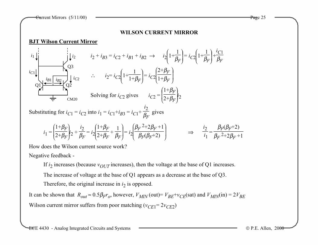
WILSON CURRENT MIRROR BJT Wilson Current Mirror
i2 + iB3 = iC2 + iB1 + iB2 → i2
1+
1βF
= iC2
1+
1βF
+iC1βF
∴ i2= iC2
1+
11+βF
= iC2
2+βF
1+βF
Solving for iC2 gives iC2 =
1+βF
2+βFi2
Substituting for iC1 = iC2 into i1 = iC1+iB3 = iC1+ i2βF
gives
i1 =
1+βF
2+βFi2 +
i2βF
= i2
1+βF
2+βF +
1βF
= i2
βF 2+2βF +1
βF(βF+2) ⇒ i2 i1
= βF(βF+2)
βF 2+2βF +1
How does the Wilson current source work? Negative feedback - If i2 increases (because vOUT increases), then the voltage at the base of Q1 increases.
The increase of voltage at the base of Q1 appears as a decrease at the base of Q3. Therefore, the original increase in i2 is opposed.
It can be shown that Rout ≈ 0.5βFro, however, VMIN (out)= VBE+vCE(sat) and VMIN(in) = 2VBE
Wilson current mirror suffers from poor matching (vCE1= 2vCE2)
CM20
Q1 Q2
i1 i2
Q3iC1
iC2iB1 iB2

Current Mirrors (5/11/00) Page 26
ECE 4430 - Analog Integrated Circuits and Systems P.E. Allen, 2000
Wilson MOS Current Mirror
iI iOM3
M2M1
gm3vgs3 rds3
gm2vgs2 rds2gm1vgs1 rds1
+
-
vout
iout
Fig. 4.4-11
+ -vgs3+
-
vgs2=vgs1
+
-
vin
iin
Uses negative series feedback to achieve higher output resistance. • Rout = ? (iin=0) vout = rds2(iout - gm3vgs3) + vgs2
vgs2 = iout
gm2+gds2 =
rds2iout1+gm2rds2
and vgs3 = -gm1rds1vgs2 - vgs2= -(1+gm1rds1)vgs2
∴ vout = rds2iout + gm3rds2(1+gm1rds1)vgs2 = iout
rds3+rds2
1+gm3rds2+gm1rds1gm3rds3
1 + gm2rds2
Rout = rds3+rds2
1+gm3rds2+gm1rds1gm3rds3
1 + gm2rds2 ≈
gm1rds1gm3rds3gm2

Current Mirrors (5/11/00) Page 27
ECE 4430 - Analog Integrated Circuits and Systems P.E. Allen, 2000
Wilson Current Mirror - Continued • Rin = ? (vout = 0)
iin ≈ gm1vgs1 = gm1gm3vgs3
gm2+gds2+gds3 ≈
gm1gm3vgs3gm2
vgs3 = vin - vgs1= vin - gm1gm3vgs3
gm2 ⇒ vgs3 =
vin
1 + gm1gm3
gm2
∴ iin ≈ gm1gm3 vingm2 +gm3
⇒ Rin = gm2 +gm3 gm1gm3
• VMIN(in) = 2(VT+VON)
• VMIN(out) = VT + 2VON
• Current gain matching - poor, vDS1 ≠ vDS2

Current Mirrors (5/11/00) Page 28
ECE 4430 - Analog Integrated Circuits and Systems P.E. Allen, 2000
Evolution of the Regulated Cascode Current Mirror from the Wilson Current Mirror
iI iOM3
M2
M1
Wilson Current Mirror Redrawn
iI iOM3
M2
M1
VBias2
Regulated Cascode Current Sink
Fig. 4.4-12

Current Mirrors (5/11/00) Page 29
ECE 4430 - Analog Integrated Circuits and Systems P.E. Allen, 2000
REGULATED CASCODE CURRENT MIRROR MOS Regulated Cascode Current Mirror
IBias iOM3
M2
M1
iI
M4
FIG. 4.4-13 • Rout ≈ gm2rds3
• Rin ≈ 1
gm4
• VMIN(out) = VT+2VON (Can be reduced to 2VON)
• VMIN(in) = VT+VON (Can be reduced to VON)
• Current gain matching - good as long as vDS4 = vDS2

Current Mirrors (5/11/00) Page 30
ECE 4430 - Analog Integrated Circuits and Systems P.E. Allen, 2000
BiCMOS Regulated Cascode Current Mirror Circuit:
IBias
VDD
CM21
Q1 Q2
M3
M4M5
+
-
vOUT
iOUT
M13
M6 M7
M8iIN
M9M10
M12M11 M14 M15 M16 M17
I6 I4I7 I5
+
-
vCE(sat)+
-
vCE(sat)
Constraints: Let I4 = I6 and I5 = I6. If the W/L values of M4-M7 are equal than these currents can be used to set the collector-emitter voltages of Q1 and Q2.
Rin ≈ (gds7+gds14)(gπ1+gπ2)
gm1gm7gm8 , Rout ≈ ro1gm3rds3gm5(rds5||rds8), VMIN(out) = VMIN(in) = vCE(sat)
and the current matching will be excellent.

Current Mirrors (5/11/00) Page 31
ECE 4430 - Analog Integrated Circuits and Systems P.E. Allen, 2000
SUMMARY Summary of MOS Current Mirrors
Current Mirror Accuracy Output Resistance
Input Resistance
Minimum Output Voltage
Minimum Input Voltage
Simple Poor rds 1
gm VON VT+VON
Cascode Excellent gmrds2 2gm
VT+2VON 2(VT+VON)
Wide Output Swing Cascode
Excellent gmrds2 1gm
2VON VT+VON
Self-biased Cascode
Excellent gmrds2 R + 1
gm 2VON VT+2VON
Wilson Poor gmrds2 2gm
2(VT+VON) VT+2VON
Regulated Cascode Good-Excellent gm2rds3 1gm
VT+2VON
(min. is 2VON) VT+VON
(min. is VON)

Current Mirrors (5/11/00) Page 32
ECE 4430 - Analog Integrated Circuits and Systems P.E. Allen, 2000
Summary of BJT Current Mirrors
Current Mirror Accuracy Output Resistance
Input Resistance
Minimum Output Voltage
Minimum Input Voltage
Simple Poor ro 1gm
VCE(sat) VBE
Cascode Excellent βFro 2gm
VCE(sat)+VBE 2VBE
Wide Output Swing Cascode
Excellent βFro 1gm
2VCE(sat) VBE
Self-biased Cascode
Excellent βFro R + 1
gm 2VCE(sat) VCE(sat)+VBE
Wilson Poor βFro 2gm
VCE(sat)+VBE VCE(sat)+VBE
Regulated Cascode Good-Excellent βFro 1gm
or less VCE(sat)* VCE(sat)*
* One can design the regulated cascode so that effectively the minimum value of VMIN (out) is just VCE(sat).