
Ultrabroadband radio-frequency arbitrary waveform generation with ...

Analytical study on arbitrary waveform generation by MEMS micro mirror arrays
Salih K. Kalyoncu,1 Yuewang Huang,1 Qi Song,1 and Ozdal Boyraz1,2* 1EECS Department, University of California, Irvine, 92697, USA
2EE Department, founding member, Istanbul Sehir University, Istanbul, Turkey *[email protected]
Abstract: We provide analytical modeling and the detailed procedure that is used in recently proposed arbitrary waveform generation technique by using MEMS digital micro-mirror arrays. We estimate the achievable temporal resolution, repetition rate, modulation index and the rise/fall times of the final waveform as figure of merit in the proposed systems. We show that reducing the diffraction limit via increasing the ratio of beam size to lens focal length (>0.075) and the spatial modulation down to single mirror pitch size (10.8μm), waveforms up to 18GHz repetition rates with >90% modulation index and <100ps rise times are achievable. Theoretical calculations are compared with experimental generation of 120MHz square waves and 160MHz sawtooth waves and obtained good agreement.
©2012 Optical Society of America
OCIS codes: (050.1970) Diffractive optics; (070.6120) Spatial light modulators; (230.3990) Micro-optical devices.
References and links 1. L. J. Mullen, A. J. C. Vieira, P. R. Herezfeld, and V. M. Contarino, “Application of RADAR technology to aerial
LIDAR systems for enhancement of shallow underwater target detection,” IEEE Trans. Microw. Theory Tech. 43(9), 2370–2377 (1995).
2. B. Jalali, P. Kelkar, and V. Saxena, “Photonic arbitrary waveform generator,” in Proc. 14th Annu. Meeting IEEE Lasers Electro-Optics Soc. 1, 253–254 (2001).
3. S. Poinsot, H. Porte, J.-P. Goedgebuer, W. T. Rhodes, and B. Boussert, “Continuous radio-frequency tuning of an optoelectronic oscillator with dispersive feedback,” Opt. Lett. 27(15), 1300–1302 (2002).
4. T. Yilmaz, C. M. DePriest, T. Turpin, J. H. Abeles, and P. J. Delfyett, “Toward a photonic arbitrary waveform generator using modelocked external cavity semiconductor laser,” IEEE Photon. Technol. Lett. 14(11), 1608–1610 (2002).
5. H. Chi and J. Yao, “Symmetrical waveform generation based on temporal pulse shaping using amplitude-only modulator,” Electron. Lett. 43(7), 415–417 (2007).
6. C. Wang and J. Yao, “Large time-bandwidth product microwave arbitrary waveform generation using a spatially discrete chirped fiber Bragg grating,” J. Lightwave Technol. 28(11), 1652–1660 (2010).
7. M. Bolea, J. Mora, B. Ortega, and J. Capmany, “Optical arbitrary waveform generator using incoherent microwave photonic filtering,” IEEE Photon. Technol. Lett. 23(10), 618–620 (2011).
8. J. D. McKinney, D. E. Leaird, and A. M. Weiner, “Millimeter-wave arbitrary waveform generation with a direct space-to-time pulse shaper,” Opt. Lett. 27(15), 1345–1347 (2002).
9. A. M. Weiner, “Femtosecond optical pulse shaping and processing,” Prog. Quantum Electron. 19(3), 161–237 (1995).
10. J. Chou, Y. Han, and B. Jalali, “Adaptive RF-Photonic arbitrary waveform generator,” IEEE Photon. Technol. Lett. 15(4), 581–583 (2003).
11. D. L. P. Texas Instruments, “DLP 0.55XGA Chipset,” (Texas Instruments 2010). http://www.ti.com/lit/ml/dlpb003/dlpb003.pdf
12. R. S. Nesbitt, S. L. Smith, R. A. Molnar, and S. A. Benton, “Holographic recording using a digital micromirror device,” Proc. SPIE 3637, 12–20 (1999).
13. I. W. Jung, J. S. Wang, and O. Solgaard, “Optical pattern generation using a spatial light modulator for maskless lithography,” IEEE J. Sel. Top. Quantum Electron. 13(2), 147–154 (2007).
14. D. Dudley, W. Duncan, and J. Slaughter, “Emerging Digital Micromirror Device (DMD) applications,” Proc. SPIE 4985, 14–25 (2003).
15. S. K. Nayar, V. Branzoi, and T. E. Boult, “Programmable imaging using a digital micromirror array,” In Proc. of IEEE Conference on Computer Vision and Pattern Recognition (CVPR) I, 436–443 (2004).
#174197 - $15.00 USD Received 23 Aug 2012; revised 11 Nov 2012; accepted 12 Nov 2012; published 28 Nov 2012(C) 2012 OSA 3 December 2012 / Vol. 20, No. 25 / OPTICS EXPRESS 27542

16. S. K. Kalyoncu, Y. Huang, Q. Song, and O. Boyraz, “Fast arbitrary waveform generation by using digital micro mirror arrays,” IEEE Photonics Conference, paper TuK 4, San Francisco, Sept. 2012.
17. S. K. Kalyoncu, Y. Huang, Q. Song and O. Boyraz, “Fast arbitrary waveform generation by using digital micro mirror arrays,” IEEE Photon. Technol. Lett. (To be Appear In Photonics Technology Letters).
18. M. L. Hsieh, “Modulation transfer function of Digital Micromirror Device,” Opt. Eng. 45(3), 034001 (2006). 19. O. Boyraz, J. Kim, M. N. Islam, and B. Jalali, “10 Gb/s multiple wavelength, coherent short pulse source based
on spectral carving of supercontinuum generated in fibers,” J. Lightwave Technol. 18(12), 2167–2175 (2000).
1. Introduction
Arbitrary waveform generators (AWGs) find many applications in wide range of fields varying from wideband communication and instrument diagnostics to remote sensing and radar systems. Photonic AWGs provide wider bandwidth and higher dynamic range resolution and hence can complement the electronic AWG techniques in many applications [1,2]. Various photonic techniques which significantly improve the current state of art millimeter wave and microwave AWG have been proposed and demonstrated. The narrow band techniques which enable to generate tunable gigahertz waveforms through RF interference by employing a tunable laser diode source, electrooptic modulator, and fiber delay lines [3] and through beating of different longitudinal laser modes, which are independently phase or amplitude modulated to produce arbitrarily shaped beat signals, by utilizing mode-locked laser diode combined with a wavelength-division-demultiplexing [4] have been demonstrated. Using arrayed waveguide grating as a wavelength-division-multiplexing (WDM) scheme with a series of optical attenuators and delay lines as well permits to achieve amplitude and phase modulated gigahertz RF waveforms [2]. This technique, however, requires adapting the wavelength selective delay lines for each specific RF waveform and thus complicates the reconfigurability. In addition, all-fiber based methods such as temporal pulse shaping, spectral shaping and microwave filtering followed by frequency-to-time mapping have been recently proposed to generate desired RF waveforms [5–7]. Moreover, free space AWG techniques using high rate tailored pulse sequences produced through the direct space-to-time pulse shaper generating amplitude equalized and frequency modulated RF waveforms up to 50 GHz [8] and time stretched reprogrammable system producing waveforms up to 10GHz by shaping the spectrum of the broadband source spatially after being mapped over the modulator which relies on liquid crystal horizontal pixel arrays providing controllability over the amplitude and phase of the incident light [9,10] have been previously proposed. Recently, new digital micro-mirror device (DMD) based on the DLPTM technology (Texas Instruments, Dallas, TX) enabling two dimensional mapping and modulation via 2D pixel arrays, high resolution, high reflection, exceptional stability and excellent controllability over thousands of individual micro mirrors have been commercialized. In comparison to most commonly used liquid crystal display (LCD) technology, such devices providing extremely faster switching speeds (<30μs) between different types of modulation patterns, less attenuation (higher fill factor of %90 than the LC with %70), ~6.6 times higher power transfer efficiency, ~11 times higher contrast ratio, as twice as higher diffraction efficiency of %88, feasibility for wide range of wavelengths (UV to NIR) can be used as a digital spatial light modulator [11,12]. Up to date MEMS micro-mirror arrays have been proposed for such many application as programmable imaging, display technologies, spectroscopy, microscopy, 3D metrology, and maskless lithography [13–15]. However, use of such devices for arbitrary waveform generation has not been utilized.
Recently, we have experimentally demonstrated novel method for optical arbitrary waveform generation that utilizes DMD technology [16,17]. We show that utilizing DMD technology allows AWG with bandwidth up to 18GHz with reconfigurability rate beyond 32.5kHz. In this paper we discuss the procedure that is used in AWG in detail and provide analytical modeling. Additionally, we discuss the limits on the achievable spatial and temporal resolution of the proposed technique based on currently available digital mirror technologies. We calculate the repetition rate, modulation index and the rise/fall times of the
#174197 - $15.00 USD Received 23 Aug 2012; revised 11 Nov 2012; accepted 12 Nov 2012; published 28 Nov 2012(C) 2012 OSA 3 December 2012 / Vol. 20, No. 25 / OPTICS EXPRESS 27543

final waveform as figure of merit. We show that reducing the diffraction limit by increasing the ratio of beam size to lens focal length (>0.1) and spatial modulation down to single mirror pitch size (10.8μm), waveforms up to 18GHz repetition rates with >90% modulation index and <100ps rise times can be achievable by utilizing −675 ps/nm dispersion. The system temporal performance increases with the amount of dispersion. We also compare the experimental results with theoretical estimates on generated square and sawtooth waveforms at 120MHz and 160MHz, respectively. We show that the analytical estimates match the experimental results.
2. AWG configuration and theoretical analysis
We investigated the optically assisted AWG system, which is mainly designed by combining the broadband illumination, wavelength-to-time mapping, space-wavelength mapping and spectral shaping modules, Fig. 1. The supercontinuum (SC) pulses centered at 1590nm are used as 20nm wide broadband source to capture the spectral modulation that is transformed into RF signals after time wavelength mapping [10]. In the first stage, the broadband SC pulses are propagated through the dispersion compensation module (DCM) with −675 ps/nm dispersion to map the spectral information into temporal waveform. Then, the spectral content of the time stretched SC pulses are mapped over the focal plane by diffractive optics which is composed of a blazed diffraction grating with 600 lines/mm grove density and a Fourier lens with 200mm focal length to collimate the dispersed wavelengths and to focus the beam for better resolution. After being mapped over the focal plane, the spectrum of the pulses is shaped by 1024 X 768 micro-mirror arrays used as a digital spatial light modulator. The pattern on the DMD is electronically tunable and the pattern is set according to the desired waveforms. The temporally and spectrally modulated signals are captured by an optical detector connected to a real time oscilloscope.
Fig. 1. Functional block diagram for all-optical arbitrary waveform generation by using micro-mirror arrays. SC: Supercontinuum, DCM: Dispersion compensating module, DMD: Digital micro-mirror device, PC: Personal computer, OSC: Oscilloscope.
2.1. Resolution analysis
The resolution of the proposed AWG system is analyzed in terms of the spatial and spectral resolution of the pulse shaping module [9,10] and the temporal resolution of the detection system to assess the limit on the achievable RF waveforms. The pulse shaping mechanism is the key module of the proposed AWG system and consists of space wavelength mapping, namely the spatial dispersion of wavelengths via diffractive element, and the focusing system which focuses the collimated beam on to the spatial light modulator by a cylindrical lens [9,10]. The spatial resolution of the focusing system, namely the minimum focal size, limits the smallest detectable feature on the image plane (refers to DMD) due to the diffraction limit and depends on the wavelength (λ), the focal length (f) of the Fourier lens and the beam size (d) which is defined as the aperture diameter if the plane wave is considered or the spatial full width at half maximum width (FWHM) if the Gaussian wave is considered, Fig. 2(a). Here, we analyzed the spatial and spectral resolution performance of the pulse shaping module for
#174197 - $15.00 USD Received 23 Aug 2012; revised 11 Nov 2012; accepted 12 Nov 2012; published 28 Nov 2012(C) 2012 OSA 3 December 2012 / Vol. 20, No. 25 / OPTICS EXPRESS 27544
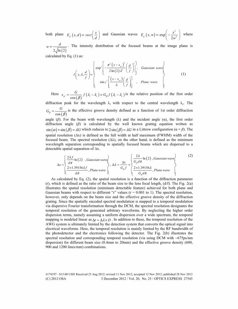
both plane ( ),p
xE x d rect
d ∝
and Gaussian waves ( )2
2, exp
2g
xE x w
w
∝ −
where
( )2 ln 2
dw = . The intensity distribution of the focused beams at the image plane is
calculated by Eq. (1) as:
( )( )
( )
2 22
2
2
2
exp ,2 ln 2
, ,
sin ,
pi
pi
x x dGaussian wave
fdI x
f x x dc Plane wave
f
π
λλ
λ
−−
∝−
(1)
Here ( ) ( ) ( )
cospi i c i c
Gx f G fβλ λ λ λ
β≈ − = − is the relative position of the first order
diffraction peak for the wavelength λi with respect to the central wavelength λc. The
( )cos
GGβ β
= is the effective groove density defined as a function of 1st order diffraction
angle (β). For the beam with wavelength (λ) and the incident angle (α), the first order diffraction angle (β) is calculated by the well known grating equation written as
( ) ( )sin sin Gα β λ+ = which reduces to ( )2sin Gβ λ= in a Littrow configuration (α = β). The
spatial resolution (∆x) is defined as the full width at half maximum (FWHM) width of the focused beam. The spectral resolution (Δλ), on the other hand, is defined as the minimum wavelength separation corresponding to spatially focused beams which are dispersed to a detectable spatial separation of ∆x.
( ) ( )22 ln 2 ,ln 2 ,
,2 1.39156 2 1.39156
, ,
f Gaussian waveGaussian wave G dxdx
f G fPlane wave Plane wave
d G d
β
β
β
λλππ λ
λ λπ π
ΔΔ ≈ Δ ≈ =
× ×
(2)
As calculated by Eq. (2), the spatial resolution is a function of the diffraction parameter (r), which is defined as the ratio of the beam size to the lens focal length, (d/f). The Fig. 2(a) illustrates the spatial resolution (minimum detectable feature) achieved for both plane and Gaussian beams with respect to different “r” values (r = 0.001 to 1). The spectral resolution, however, only depends on the beam size and the effective groove density of the diffraction grating. Since the spatially encoded spectral modulation is mapped to a temporal modulation via dispersive Fourier transformation through the DCM, the spectral resolution designates the temporal resolution of the generated arbitrary waveforms. By neglecting the higher order dispersion terms, namely assuming a uniform dispersion over a wide spectrum, the temporal mapping is modeled linear as t DλΔ ≈ Δ × . In addition to these, the temporal resolution of the AWG system is ultimately limited by the detection system that converts the optical signal into electrical waveforms. Here, the temporal resolution is mainly limited by the RF bandwidth of the photodetector and the electronics following the detector. The Fig. 2(b) illustrates the spectral resolution and corresponding temporal resolution (via using DCM with −675ps/nm dispersion) for different beam size (0.4mm to 20mm) and the effective groove density (600, 900 and 1200 lines/mm) combinations.
#174197 - $15.00 USD Received 23 Aug 2012; revised 11 Nov 2012; accepted 12 Nov 2012; published 28 Nov 2012(C) 2012 OSA 3 December 2012 / Vol. 20, No. 25 / OPTICS EXPRESS 27545

Fig. 2. The spatial resolution (a) of the focusing system depends on the diffraction limit and is impoved by increasing diffraction parameter, r. The spectral and temporal resolution (calculated for D = −675ps/nm) mainly depends on the beam size, d and the effective groove density,Gβ (b).
2.2 Spatial light modulation
The spatial light modulator is placed at the focal plane to shape the spectrum of the broadband source properly for the desired waveform. The approach we propose uses the MEMS based digital micro-mirror array device (DMD). The particular DMD considered in the experimental setup and in these analytical calculations is a 0.55-inch diagonal mirror arrays consisting of 1024x768 individually addressable aluminum micro mirrors with 10.8µm pitch size, Fig. 3(a). Each mirror can be assigned to discrete states of ON ( + 12° rotation) or OFF (−12° rotation), which can be refreshed at a frame rate of 5 kHz, to control the direction of light [11]. The mirrors having a fill factor of %90 provide a high optical efficiency and are capable of modulating broadband light ranging from ultraviolent to infrared wavelengths. The DMD mirrors are also protected by a cover glass which is coated to operate for desired spectral window [14]. Among these the frame rate is particularly important and it determines the ultimate rate at which we can reconfigure the whole waveform and also the maximum temporal width of a waveform package, as long as the laser repetition rate is adjusted accordingly. With the recent MEMS micro-mirror technologies, up to 32.5 kHz pattern rate with a fast switching speed of approximately 30µs between the states allowing for fast display of illumination patterns can be achieved.
Fig. 3. The micro mirrors inbuilted on DMD with having 10.8 microns pitch size and ~1micron
gap in between (a) can be oriented with high precision and speed at + 12 or + 12 degrees [13].
A sample (b) implemented ON-OFF modulation pattern on DMD [19].
#174197 - $15.00 USD Received 23 Aug 2012; revised 11 Nov 2012; accepted 12 Nov 2012; published 28 Nov 2012(C) 2012 OSA 3 December 2012 / Vol. 20, No. 25 / OPTICS EXPRESS 27546

2.2.1 Square waveform generation
In order to generate an arbitrary waveform with a desired shape and frequency binary image patterns are created on the DMD to set the states. The shape of the waveform corresponds to the image of the binary pattern. For instance, in order to generate square waveforms binary image patterns similar to the samples shown in Fig. 4 are fed into the DMD. These vertical strip type patterns with varying spatial frequency (in terms of the number of mirrors) function as a periodic rectangular spectral filter. Black lines correspond to the OFF state of mirrors and white lines correspond to ON state of mirrors.
Fig. 4. The sample binary image patterns created on DMD to generate square waveforms with different spatial frequencies. Patterns with spatial period of 60mirrors/period (a), 120mirrors/period (b) and 200mirrors/period (c).
By carefully selecting the bandwidth of SC pulses we can generate periodic waveforms encoded on a single laser pulse. Using parallel system or utilizing the different diffraction orders from the digital light mirrors, on the other hand, waveforms which appear longer period of time, namely aperiodic with respect to laser repetition rate can also be generated. The frequency of the generated RF waveforms on a single pulse is basically determined by the spatial light modulator and the dispersive unit. As illustrated in Fig. 5(a) that decreasing the pattern’s spatial modulation down to single mirror pitch size (10.8μm) and using gratings with higher groove density improves the spectral allocation (up to 18GHz temporal repetition rates can be achieved by −675ps/nm) so that further by using lower dispersion DCMs (~17 times higher modulation rates can be obtained by using −40ps/nm dispersive fiber as employed in [10]), the temporal frequency of the output waveforms can be increased.
Fig. 5. The spectral modulation and the corresponding temporal frequency (calculated for D = −675ps/nm) of the RF waveforms depends on the spatial modulation period and the effective groove density (a). Analytically generated square waveforms for different spatial modulation periods,P are illustrated in (b).
#174197 - $15.00 USD Received 23 Aug 2012; revised 11 Nov 2012; accepted 12 Nov 2012; published 28 Nov 2012(C) 2012 OSA 3 December 2012 / Vol. 20, No. 25 / OPTICS EXPRESS 27547

The accuracy and the RF bandwidth of generated waveforms are also affected by the diffraction parameter (r) and the spatial period of the patterns. We analyzed the generated waveforms in terms of the modulation index and the sharpness of the rise/fall edges. The modulation index is defined as ( ) ( )max min max min/m y y y y= − + and mainly depends on the
diffraction parameter (r). For the same spatial modulation frequency, increase in the ratio of
the beam size to lens focal length improves the spatial resolution fx
d
λ Δ ∝
so that the RF
waveforms which are the images of the patterns becomes sharper on the edges and higher in modulation index, Figs. 6(b)-6(d). In addition, for the same diffraction parameter (d/f), decrease in the pattern’s spatial period causes the edges to get closer, rounds and thus reduces the modulation index, Figs. 6(a)-6(c). The minimum spatial modulation period required to obtain a modulation index >90% is also calculated for each diffraction parameter, Figs. 6(a)-6(c).
Fig. 6. The modulation index (m) with respect to spatial modulation period and the diffraction parameter (r) is calculated for both Gaussian (a) and Plane (c) beams. Due to the difference in the definition of the beam size, which is the aperture diameter if the plane wave is considered and the spatial FWHM width if the Gaussian wave is considered, the plane beam becomes comparably narrower and cause the modulation index to be dropped abruptly. The inset figures shows the required modulation period to obtain m>90%. Analytically generated waveforms for diffrent diffraction parameters are illustrated in (b-d)
#174197 - $15.00 USD Received 23 Aug 2012; revised 11 Nov 2012; accepted 12 Nov 2012; published 28 Nov 2012(C) 2012 OSA 3 December 2012 / Vol. 20, No. 25 / OPTICS EXPRESS 27548

The other key concept to evaluate the characteristics of the generated waveforms is the maximum achievable RF bandwidth, namely the sharpness of the rise/fall edges. The spectral (δλR) or the temporal (τR) rise refers to the increment required for a waveform to change from a specified low value (10%) to a specified high value (90%). As the spatial modulation period increases, the rounding effects disappear, the edges become clearer and the edge slope becomes constant, Figs. 7(a)-7(c). The actual rise/fall time can be improved by increasing the beam size, d (the effect of the lens focal length is almost negligible) and by using gratings with higher groove density (G), Figs. 7(b)-7(d).
Fig. 7. The spectral (δλR) and the temporal (τR) rise at the waveform edges due to spatial modulation period (a-c) and the beam size (b-d) for Gaussian and Plane beams, respectively. The inset figures shows that the effect of lens focal length on δλR and τR is almost negligible.
2.2.2 Sawtooth waveform generation
The DMD can display both binary and grayscale images with high frame rates. Contrary to binary images for which the micro mirrors are only assigned to either ON or OFF states, to achieve grayscale images, however, requires fast switching of the mirrors between two binary states by properly adjusting the percentage of the time the mirror is at ON state during the refresh time. The DMD chipset used in this experiment can be refreshed up to 5kHz (200μs refresh time) and 500Hz (2ms refresh time) for binary and grayscale (up to 8bits, 256 levels, toning) images, respectively. However, since the temporal window (temporal width of the SC pulses) to catch the pattern modulation is much shorter than the DMD refresh time, it disables
#174197 - $15.00 USD Received 23 Aug 2012; revised 11 Nov 2012; accepted 12 Nov 2012; published 28 Nov 2012(C) 2012 OSA 3 December 2012 / Vol. 20, No. 25 / OPTICS EXPRESS 27549

to utilize the averaging of dynamic patterns. Thus, static assignment of the micro mirrors can only be used for the waveform generation. On the other hand, to enable amplitude modulation or to generate complex waveforms such as sawtooth or triangle, which includes grayscale amplitudes, special patterns has to be created. Two different approaches have been proposed to create appropriate binary patterns to achieve grayscale modulation.
In the first approach, the two dimensional mapping/modulation capability of DMD via 1024 X 768 individually addressable digital micro mirror arrays is proposed to accomplish amplitude quantization. To enable 2D modulation, spatially dispersed and collimated beam (considered as 1D wavelength to space mapping) has to be expanded to illuminate a sufficient area over the DMD. Through assigning the mirrors in horizontal direction for the temporal sampling and the mirrors in the vertical direction for the amplitude quantization, it is possible to generate complex waveforms by adjusting the number of vertical ON state mirrors accordingly to set the quantization levels, Fig. 8.
Fig. 8. The 2-D amplitude quantization model for sawtooth waveform generation. The sample modulation scheme employed on DMD with 128 horizontal mirrors/period and 8 amplitude quantization levels (a). The sample binary image pattern with 128 horizontal mirrors/period and 320 vertical mirrors (40 mirrors /each level) created on DMD to generate sawtooth waveform (b).
In the second approach, using so called pulse width modulation among the combined group of mirrors enables one dimensional amplitude quantization. The pre-defined modulation period (in terms of the pixels/mirrors), is divided into sub-periods to define each quantization level for which the number of the mirrors at ON state is set accordingly, Fig. 9(a). The binary image patterns created due to second approach similar to the sample shown in Fig. 9(b) are used in the experiment to generate the sawtooth waveforms with varying spatial period.
Fig. 9. The so-called pulse width modulation model for sawtooth waveform generation. The sample modulation scheme employed on DMD with 128 mirrors/period and 8 amplitude quantization levels (a). The sample binary image pattern with 128 horizontal mirrors/period created on DMD to generate sawtooth waveform (b).
#174197 - $15.00 USD Received 23 Aug 2012; revised 11 Nov 2012; accepted 12 Nov 2012; published 28 Nov 2012(C) 2012 OSA 3 December 2012 / Vol. 20, No. 25 / OPTICS EXPRESS 27550

3. Experimental results
The experimental setup for optical AWG used to test our theoretical model is illustrated in Fig. 10. Supercontinuum pulses are generated to provide broadband source by propagating the Mode Locked Laser pulses (at 1550nm with <1ps pulse width and 20MHz repetition rate) through the amplifier (EDFA: Erbium Doped Fiber Amplifier) and the cascaded single mode, dispersion shifted and nonlinear fiber patch cords [18]. Band pass filter (CWDM: Coarse Wavelength Division Multiplexing) centered at 1590nm is used to carve out ~20nm nearly-flat portion of the spectrum. Generated SC pulses are then wavelength-to-time mapped through the dispersion compensation module (DCM with −675ps/nm) for real time detection. The optical pulses, on the other hand, are highly attenuated while passing through the system. The system losses are mainly due to the DCM (~2.1 dB insertion loss) and the DMD which induces single pass attenuation of ~45% by considering the beam wavelength (1590nm), micro-mirror reflectivity (~90%), active area (~90%), diffraction efficiency (%88) and the transmission of the protective cover glass on the micro mirrors (~90% if coated for NIR and ~75% if coated for visible) [14]. In order to compensate the system losses and to obtain a better signal to noise ratio, a flat gain Raman amplifier is designed to provide a uniform amplification through the DCM. The Raman amplification with ~10dB net gain and <0.5dB gain ripple is introduced by using diode lasers with different wavelengths in a hybrid pumping configuration. Amplified and temporally stretched broadband pulses are spatially dispersed and collimated on to the DMD (1024x768 mirror array). The spectrally and temporally modulated pulses via DMD are captured by the photo detector (>1.2GHz bandwidth), which is placed through the mirrors’ ON state direction, connected to real time storage oscilloscope with 8GHz bandwidth. The DMD chipset used in the experiment is protected by a cover glass, which is anti-reflective coated for visible light. Under broadband and near infrared illumination, a strong interference results from the Fabry Perot effect between the micro-mirrors and the cover glass. This spectral interference transforms to a temporal modulation of ~1.8GHz through the DCM (−675ps/nm). As a result, a low pass filter with 1GHz cut-off is used after the detector to eliminate this undesired interference.
Fig. 10. The experimental setup of all optical arbitrary waveform generator (AWG). MLL: Mode locked laser, EDFA: Erbium doped fiber amplifier, SC: Supercontinuum, BPF: Band pass filter.
In the experiment, we have used collimated beam with a Gaussian profile having ~0.87mm beam diameter, Fourier lenses with 200mm (L1) and 30mm (L2) focal lengths and a blazed diffraction grating with 600lines/mm. The DMD is loaded with the appropriate patterns, similar to Fig. 4 and Fig. 9(b), with 180mirrors/period and 162 mirrors/period for
#174197 - $15.00 USD Received 23 Aug 2012; revised 11 Nov 2012; accepted 12 Nov 2012; published 28 Nov 2012(C) 2012 OSA 3 December 2012 / Vol. 20, No. 25 / OPTICS EXPRESS 27551

square and sawtooth waveform generation, respectively. The experimentally and analytically generated square and the sawtooth waveforms are illustrated to demonstrate the concept and the correctness of the analytical model, Fig. 11. The RF waveforms illustrated in Fig. 11, are generated on a single stretched pulse, which provides nearly 13.5ns (20nm X 0.675ns) temporal window. However, since the MLL output rate is 20MHz (50ns period), there is ~36.5ns time interval between each stretched pulses, in which the output light power is zero. This interval can be reduced or prevented by increasing the temporal width of stretched pulse to occupy the entire MLL pulse period via using wider spectral width or longer dispersion compensating module (Δλ × D≈50ns). In addition, using such a parallel interleaved configuration with appropriate delay lines can fill this time gap to perform a real continuous time operation. In this manuscript we focus on single channel application.
Fig. 11. The analytical and experimental results for the generated square waveform at 120MHz (a) and for the sawtooth waveform at 160MHz (b). The weak high frequency modulation appears on the analytically generated sawtooth waveform (b) results from the individual square
type modulation of the sub-periods of the pattern used to generate sawtooth waveforms (Fig. 9). This weak modulation on the sawtooth waveform and the sharp edges of the square waveform are slightly smoothened due to the 1GHz LPF used in the experimental setup.
3. Summary
We have proposed a new approach for all optical AWG by using MEMS based micro mirror arrays as a digital spatial light modulator. We described the procedure that is used in AWG in detail and provide analytical modeling. Additionally, we discuss the limits of the proposed technique based on currently available digital mirror technologies. As a performance criteria, the achievable temporal frequency, modulation index and the maximum frequency bandwidth of the modulated waveforms are investigated for such different optical system parameters as the beam size, lens focal length, effective groove density and the spatial modulation frequency. The results indicates that reducing the diffraction limit via increasing the ratio of beam size to lens focal length (>0.075) and spatial modulation down to single mirror pitch size (10.8μm), waveforms up to 18GHz repetition rates with >90% modulation index and <100ps rise/fall times can be achievable by utilizing −675 ps/nm dispersion. The system temporal performance mainly depends on the dispersive unit and can be improved proportionally with the amount of dispersion. Using an initial experimental setup, we obtain 160MHz sawtooth and 120MHz square waveforms and compared with analytical counterparts to illustrate the agreement with the analytical estimates. Based on the state of the art MEMS
#174197 - $15.00 USD Received 23 Aug 2012; revised 11 Nov 2012; accepted 12 Nov 2012; published 28 Nov 2012(C) 2012 OSA 3 December 2012 / Vol. 20, No. 25 / OPTICS EXPRESS 27552

digital mirror technology, we estimate that waveforms with 1GHz rate reconfigurable in ~30μs are achievable by using proposed approach. Using an effective feedback algorithm, the system would converge to high accuracy waveforms with minimum achievable waveform error by compensating for the system non-idealities such as non-uniformity of the SC source and the system distortions through the patterns fed into the mirrors.
Acknowledgment
This work is supported by DARPA Young Faculty Award, #66001-10-1-4036, DARPA RADER Program and EU grant PIRG07-GA-2010-268370.
#174197 - $15.00 USD Received 23 Aug 2012; revised 11 Nov 2012; accepted 12 Nov 2012; published 28 Nov 2012(C) 2012 OSA 3 December 2012 / Vol. 20, No. 25 / OPTICS EXPRESS 27553