Analytical Modeling and TCAD Simulation of a Quanta …ericfossum.com/Publications/Papers/2017 IEEE...
10
Received 9 August 2016; revised 5 October 2016; accepted 13 October 2016. Date of publication 19 October 2016; date of current version 20 December 2016. The review of this paper was arranged by Editor A. G. Unil Perera. Digital Object Identifier 10.1109/JEDS.2016.2618721 Analytical Modeling and TCAD Simulation of a Quanta Image Sensor Jot Device With a JFET Source-Follower for Deep Sub-Electron Read Noise JIAJU MA (Student Member, IEEE), AND ERIC R. FOSSUM (Fellow, IEEE) Thayer School of Engineering, Dartmouth College, Hanover, NH 03755, USA CORRESPONDING AUTHOR: E. R. FOSSUM (e-mail: [email protected]) This work was supported by Rambus. ABSTRACT A novel quanta image sensor (QIS) jot device with a CMOS compatible junction-field effect transistor (JFET) source follower (SF) is introduced. The device is proposed to further reduce the read noise of QIS jots and ultimately realize a read noise of 0.15e-r.m.s. for accurate photoelectron counting. We take advantage of the small gate capacitance in a p-channel JFET SF to reduce the total capacitance of the floating diffusion, which yields a greatly improved conversion gain of 1.38 mV/e- in TCAD simulation compared to MOSFET SF with the same pitch size. Lower 1/f noise is also anticipated yielding a low input-referred read noise. The device is designed in a 45 nm CMOS image sensor process. The fundamental working principles of this device are discussed, and important functionalities are analyzed with simulation and theory. INDEX TERMS CMOS image sensor, quanta image sensor, jot device, low noise imaging, TCAD simulation. I. INTRODUCTION The quanta Image Sensor (QIS) was first proposed in 2004 as a “digital film camera” [1], [2] outlining a dif- ferent way to utilize sub-diffraction-limit (SDL) pixels. In the concept, a QIS might consist of one billion special- ized sub-micrometer-pitch pixels, which are called “jots”. The large array of jots work at a high frame rate (e.g., 1000fps) and with extremely low power consumption [3]. The small area size per jot and high frame rate ensures that the photon exposure on each jot per frame is limited to sev- eral photons. Jots detect the number of incident photons, and then output single-bit or multi-bit digital data corre- sponding to this number [4]. The final image is created by integrating the digital data both spatially over multiple jots and temporally over multiple frames [5] with image pro- cessing. If jots can count photoelectrons in each frame so accurately that counting error is negligible, noise-free jot data binning is achievable. QIS can enable many appli- cations, such as high-dynamic-range imaging in consumer photography [6], scientific imaging, security [7], and encryption [8]. In a photoelectron counting image sensor, the counting accuracy or counting error rate is impacted by many charac- teristics, and the noise floor of the signal readout chain is the dominant factor [9]. Deep sub-electron read noise (DSERN) (read noise lower than 0.5e- r.m.s.) is a prerequisite for pho- toelectron counting capability, and read noise of 0.15e- r.m.s. or lower is necessary for ultimately accurate photoelectron counting (0.04% counting error rate). The counting error rate is so sensitive that a mild increase of read noise, e.g., 0.25e-r.m.s., will increase the error rate to 1%. The photoelectron signal is converted to a voltage signal by the floating diffusion (FD) node capacitance. The voltage signal is sensed by an in-pixel SF and subsequently amplified and digitized. In low-noise image sensors, the in-pixel SF is generally the most significant contributor to the total read noise (commonly 100-200 μV r.m.s.). It is a result of higher 1/f noise caused by shrinking SF area size and lack of 2168-6734 c 2016 IEEE. Translations and content mining are permitted for academic research only. Personal use is also permitted, but republication/redistribution requires IEEE permission. VOLUME 5, NO. 1, JANUARY 2017 See http://www.ieee.org/publications_standards/publications/rights/index.html for more information. 69
Transcript of Analytical Modeling and TCAD Simulation of a Quanta …ericfossum.com/Publications/Papers/2017 IEEE...

Received 9 August 2016; revised 5 October 2016; accepted 13 October 2016. Date of publication 19 October 2016;date of current version 20 December 2016. The review of this paper was arranged by Editor A. G. Unil Perera.
Digital Object Identifier 10.1109/JEDS.2016.2618721
Analytical Modeling and TCAD Simulation ofa Quanta Image Sensor Jot Device With
a JFET Source-Follower for DeepSub-Electron Read Noise
JIAJU MA (Student Member, IEEE), AND ERIC R. FOSSUM (Fellow, IEEE)Thayer School of Engineering, Dartmouth College, Hanover, NH 03755, USA
CORRESPONDING AUTHOR: E. R. FOSSUM (e-mail: [email protected])
This work was supported by Rambus.
ABSTRACT A novel quanta image sensor (QIS) jot device with a CMOS compatible junction-field effecttransistor (JFET) source follower (SF) is introduced. The device is proposed to further reduce the readnoise of QIS jots and ultimately realize a read noise of 0.15e-r.m.s. for accurate photoelectron counting.We take advantage of the small gate capacitance in a p-channel JFET SF to reduce the total capacitance ofthe floating diffusion, which yields a greatly improved conversion gain of 1.38 mV/e- in TCAD simulationcompared to MOSFET SF with the same pitch size. Lower 1/f noise is also anticipated yielding a lowinput-referred read noise. The device is designed in a 45 nm CMOS image sensor process. The fundamentalworking principles of this device are discussed, and important functionalities are analyzed with simulationand theory.
INDEX TERMS CMOS image sensor, quanta image sensor, jot device, low noise imaging, TCADsimulation.
I. INTRODUCTIONThe quanta Image Sensor (QIS) was first proposed in2004 as a “digital film camera” [1], [2] outlining a dif-ferent way to utilize sub-diffraction-limit (SDL) pixels. Inthe concept, a QIS might consist of one billion special-ized sub-micrometer-pitch pixels, which are called “jots”.The large array of jots work at a high frame rate (e.g.,1000fps) and with extremely low power consumption [3].The small area size per jot and high frame rate ensures thatthe photon exposure on each jot per frame is limited to sev-eral photons. Jots detect the number of incident photons,and then output single-bit or multi-bit digital data corre-sponding to this number [4]. The final image is created byintegrating the digital data both spatially over multiple jotsand temporally over multiple frames [5] with image pro-cessing. If jots can count photoelectrons in each frame soaccurately that counting error is negligible, noise-free jotdata binning is achievable. QIS can enable many appli-cations, such as high-dynamic-range imaging in consumer
photography [6], scientific imaging, security [7], andencryption [8].In a photoelectron counting image sensor, the counting
accuracy or counting error rate is impacted by many charac-teristics, and the noise floor of the signal readout chain is thedominant factor [9]. Deep sub-electron read noise (DSERN)(read noise lower than 0.5e- r.m.s.) is a prerequisite for pho-toelectron counting capability, and read noise of 0.15e- r.m.s.or lower is necessary for ultimately accurate photoelectroncounting (0.04% counting error rate). The counting errorrate is so sensitive that a mild increase of read noise,e.g., 0.25e-r.m.s., will increase the error rate to 1%.The photoelectron signal is converted to a voltage signal
by the floating diffusion (FD) node capacitance. The voltagesignal is sensed by an in-pixel SF and subsequently amplifiedand digitized. In low-noise image sensors, the in-pixel SF isgenerally the most significant contributor to the total readnoise (commonly 100-200 µV r.m.s.). It is a result of higher1/f noise caused by shrinking SF area size and lack of
2168-6734 c© 2016 IEEE. Translations and content mining are permitted for academic research only.Personal use is also permitted, but republication/redistribution requires IEEE permission.
VOLUME 5, NO. 1, JANUARY 2017 See http://www.ieee.org/publications_standards/publications/rights/index.html for more information. 69

MA and FOSSUM: ANALYTICAL MODELING AND TCAD SIMULATION OF A QIS JOT DEVICE
amplification of signal before the SF. Two major noise typesin a SF are 1/f noise and random telegraph signal (RTS).The origin of RTS is known to be related to the randomcapture and emission of channel carriers by Si-SiO2 interfacetraps [10]. There is still debate on the origin of 1/f noise, butthe most widely accepted explanation is the fluctuation ofconduction carrier population due to interface traps and thefluctuation of carrier mobility due to phonon scattering [11].Many experiments have been done to reduce SF noise.
Replacing the surface-channel SF with a buried-channelSF has been used historically in CCDs [12] and CMOSimage sensors [13]. In-pixel buried-channel SF and cor-related multiple sampling (CMS) can be used togetherfor improved noise reduction [14], [15]. Improvement innoise in minimum geometry buried-channel SF transistors inadvanced technology nodes may be less [16], perhaps due toSTI sidewall effects. In addition, three-fold SF noise reduc-tion was recently demonstrated by tuning the bandwidth ofcorrelated double sampling (CDS) circuitry [17].To reduce input-referred read noise, another approach
is to increase the signal using avalanche multiplication.This approach has been applied to CCDs [18], single-photon avalanche detectors (SPADs) [19], and CMOS imagesensors [20]. However, use of avalanche multiplication hasa number of drawbacks including high electric fields andoperating voltages, that lead to large pixel size, high darkcount rate, manufacturing challenges and reliability issues.Another approach is to increase the conversion gain by
reducing the capacitance of the floating diffusion node. Thepump-gate (PG) jot device developed by our group improvedCG to 410 µV/e- by reducing the FD parasitic capacitanceinduced by transfer gate (TG) and reset gate (RG) [21]–[23],and a best-case 0.22e- r.m.s. read noise was demonstrated.For the first time the PG jot enabled DSERN and photo-electron counting without electron multiplication, which wasa major step forward in our efforts to realize highly accuratephotoelectron counting for QIS applications. However, moreprogress needs to be made to further reduce read noise to0.15e- r.m.s. or lower. In general, QIS jot devices have goodcompatibility with most of the existing read noise reductiontechniques, but CMS requires relatively long processing timeand low temperature which may not be compatible with thehigh frame rate used with QIS. In a PG jot device, theSF gate oxide capacitance is the dominant contributor tothe total FD capacitance, so the reduction of SF size isinevitable for future improvements in CG. As is well-knownand re-verified in our PG jot devices, the reduction of SFsize leads to higher 1/f noise [22], [23], so the improvementin CG from smaller SF will be negated by higher 1/f noise,and input-referred read noise will hardly be improved. Fromthis dilemma arises the motivation for the present approach.In this paper, a jot device with a junction-field effect
transistor (JFET) SF is proposed. The JFET SF is a goodalternative because of its potential for low-noise andscalability [24], [25], which may be a solution for the SF-size-shrinking tradeoff with 1/f noise allowing for higher CG
FIGURE 1. Schematic of a jot device with a JFET SF and punch-throughreset.
and lower SF noise simultaneously compared to a PG jotwith MOSFET SF. The device is designed with TCAD sim-ulation tools in a 45nm backside illumination (BSI) processand will be fabricated in the coming year. In the followingsections, the fundamental working principles of this devicewill be discussed, and important functionalities are analyzedwith simulation and theory.
II. DEVICE DESCRIPTIONThe schematic of the jot device is shown in Fig. 1. Thejot consists of a pump-gate TG, a reset transistor, a JFETSF and a row-select transistor. The reset transistor can alsobe replaced with a punch-through reset diode for furtherimprovement in CG, and more details will be discussed inSection IV. The JFET SF has a p-type channel and n-typegate. The source (SRC) of SF is biased by a current source,and its drain (DRN) is biased to ground (GND). The pump-gate TG and photoelectron storage well (SW) have a similardesign to the previously fabricated PG jots. The 3D dop-ing profile of this device with a punch-through reset diodeobtained from TCAD simulation is depicted in Fig. 2. Asshown, FD also functions as the gate of the SF, locatedunderneath a shallow p-type channel. During the readout,photoelectrons transferred from SW to FD cause a potentialchange in the integrated gate of the JFET, or FD. This in turnmodulates the JFET current. If the JFET is used as a SF andoperates in the saturation region, the voltage on the sourcewill follow the FD potential. Because the JFET is built ona p-type substrate, the p-type source has to be isolated fromthe substrate to avoid a short-circuit current from the sourceto the bulk. The isolation is achieved by extending the FDn-well under the source and surrounding the source withSTI. Using a similar concept, a buried-channel version of
70 VOLUME 5, NO. 1, JANUARY 2017

MA and FOSSUM: ANALYTICAL MODELING AND TCAD SIMULATION OF A QIS JOT DEVICE
FIGURE 2. Doping profiles from 3D modeling in TCAD. Row Selector (RS) isnot included. 3D doping profile of a 2x1 shared jot with a JFET SF (Top).Cut-planes doping profile of SF region (XZ) and punch-through reset (RST)region (XY).
FIGURE 3. Doping profiles from 3D TCAD simulation. Cut-planes dopingprofile of buried-channel JFET SF region on XZ plane (left) and XYplane (right).
this device is also designed as shown in Fig. 3 to potentiallyfurther reduce 1/f noise from surface effects.This device enables the reduction of many FD capacitance
components. First, in a pixel with a MOSFET SF, the FDnode is connected to the gate of SF through a metal wire.In order to have an ohmic contact, the FD node needs to beheavily doped, which increases the FD-sub junction capaci-tance. In the proposed device, since the FD is integrated inthe SF, a metal connection is not necessary, therefore the dop-ing of the FD can be reduced, which yields a smaller junctioncapacitance. Second, the large gate-oxide capacitance insmall-scale a MOSFET SF, resulting from extremely thinoxide, is replaced by a relatively small junction capacitancebetween the gate and channel. A comparison of parasiticcapacitance components is depicted in Fig. 4, in which thecapacitance data of MOSFET SF device is extracted from
FIGURE 4. (a) Capacitance components in a TPG Jot with MOSFETSF [18] (left) and a JFET Jot (right). (b) Comparison of calculatedcapacitance components in the two types of jots.
the TPG jot device published in [21] and the capacitanceof this JFET SF is obtained from analytic calculation andsimulation. The result clearly shows the total FD capacitancecan be greatly reduced with a JFET SF approach.In a MOSFET SF, the interface traps on the surface and
STI side-wall interact with conduction carriers in the channel,and noise is introduced by the resulting carrier populationfluctuation and threshold fluctuation. In this JFET SF, sincethe gate is located underneath the channel and the channelis surrounded by FD instead of STI, the interface traps haveless impact on the conduction carriers and threshold. Lower1/f noise can be expected because the amount of traps inthe silicon bulk is much less than the amount of interfacetraps.
III. THEORETICAL DEVICE ANALYSISMany theoretical studies of JFET devices have beenpresented in [26]–[28]. Compared to conventional JFETdevices in [27], the device in this paper has a relativelyshort channel length, so the short channel effects becomemore important when modeling the device characteristics.Compared to typical short-channel JFETs, the gate in thisJFET is relatively lightly doped, and due to its asymmetricstructure, the conventional short-channel JFETs model can-not match the device performance properly. We felt someadditional theoretical analysis is necessary for a better under-standing of this device, but as the major design work stillrelies on TCAD simulation, a simplified 1D analytic modelwas developed to be used for verification and estimation.
A. PINCH-OFF EFFECT AND EFFECTIVE CHANNEL DEPTHIn the JFET, the channel and gate form a PN junction, andthe effective channel depth is equal to the physical channel
VOLUME 5, NO. 1, JANUARY 2017 71

MA and FOSSUM: ANALYTICAL MODELING AND TCAD SIMULATION OF A QIS JOT DEVICE
depth minus the depth of the depletion region induced bythe gate potential. The abrupt junction assumption is usedto get the channel depletion region depth:
D (x) ={
2εsβ
q
[Vbigc + Vg − Vc(x)
]} 12
(1)
where q is the elementary charge of holes, εs is the permit-tivity of silicon, Vbigc is the gate-channel built-in voltage,Vg is the gate bias voltage, and Vc(x) is the potential inthe channel at location x. β is a doping ratio coefficientdefined as:
β = NdNa
1
Na + Nd(2)
where Na and Nd are the doping concentration of the channeland the gate respectively. The coordinate system that willbe used in the following discussions is defined in Fig. 4(a):x = 0 is the origin of the channel at the source-end; andx = L is the endpoint of the channel at the drain-end, withL being the physical channel length.The channel potential is determined by the bias voltages
applied to the source VS, and the drain VD. When the JFETis setup as a SF, the drain is biased to ground and the sourcehas a positive output voltage, so the situation when VSD > 0is of most interest. Under this condition, Vc(x) decreasesgradually from the VS (at x = 0) to VD (at x = L).When the depletion region depth is equal to or greater than
the physical channel depth, pinch-off occurs. From Eq.1, itcan be anticipated that pinch-off will happen at the drain-end first as Vg increases. The pinch-off voltage is definedin [26] as:
Vp = Vbigc + VGS − VSDsat = qh2
2εsβ(3)
where h is the physical channel depth, and VSDsat is theminimum source-drain voltage to trigger pinch-off undera given gate bias VGS. As VGS increases, pinch-off willexpand towards the source, and the whole channel will becut-off when pinch-off reaches the source-end. The cut-offvoltage is then given by:
VGScutoff = Vp − Vbigc (4)
Pinch-off and cut-off effects can be observed in TCADsimulation and examples are shown in Fig. 5.
B. DRAIN CURRENT BEFORE SATURATIONA longitudinal electric field is created in the channel by VSD,resulting in a hole current from source to drain. The currentflowing through the cross-section of channel at location ofx is given by,
ID(x) = W [h− D (x)]NaqμHF(x)dVcdx
(5)
where W is the channel width, and μHF(x) is the mobil-ity of holes. In a short-channel device, the carrier mobilityreduces significantly with relatively high electric field, and
FIGURE 5. Illustrations of pinch-off and cut-off effects from TCADsimulation. Electrostatic potential profile is shown in color. The boundaryof depletion region is shown in white lines. (a) Pinch-off effect, whereVGS = 0.1V and VSD = 0.4V . (b) Cut-off effect, where VGS = 0.3V andVSD = 0.4V .
the dependence can be described by an empirical modelgiven in [26]:
μHF = μp
1 +(
μpE(x)vs
) (6)
where E(x) is the electric field, μp is the low-field holemobility that is also doping dependent, and vs is the holesaturation velocity in silicon. By integrating Eq. 5, the aver-age drain current can be obtained. The detailed calculationof this step can be found in [26]. The result is given as:
ID = − g0Vp
1 +(
μpVSDvsL
){(u2D − u2
S
)− 2
3
(u3D − u3
S
)}(7)
g0 = Wh
LNaμpq (8)
where g0 is the unit transconductance, and uS, uD are thenormalized depletion depth at the source-end and drain-endof the channel:
uS = D(0)
h=
{2εsβ
q
[Vbigc + VGS
]} 12
/h (9)
uD = D(L)
h=
{2εsβ
q
[Vbigc + VGS + VSD
]} 12
/h. (10)
C. SHORT-CHANNEL EFFECTSIn this JFET device, several short-channel effects arise asnon-negligible factors affecting device current-voltage char-acteristics. One of the several phenomena, carrier mobilityreduction due to high electric field, is already discussed in theprevious discussion. Another important effect, channel length
72 VOLUME 5, NO. 1, JANUARY 2017

MA and FOSSUM: ANALYTICAL MODELING AND TCAD SIMULATION OF A QIS JOT DEVICE
FIGURE 6. Illustration of drain-induced gate depletion in TCAD simulationwhen VGS = −0.5V and VSD = 1V . The white lines are boundaries ofdepletion region. Leff1 is the effective channel length.
modulation (CLM), is the shortening of the effective channellength with increased drain bias, which is seen as an increasein current and reduction of output resistance with increaseddrain bias. CLM caused by drain-induced gate depletion aswell as pinch-off are considered in this model.
C.1. CLM BY DRAIN-INDUCED GATE DEPLETIONAccording to Eq. 1, the amount of carriers in the chan-nel is controlled by VGS and is ideally independent of VSD.However, because the drain has much higher doping than thegate, the gate is partially depleted by the drain, as shown inFig. 6. In the depletion region, as a result of charge conser-vation the drain supplies carriers to the channel, and henceleads to a reduction in the output resistance and an increasein current. Because the depletion region width xGD is of thesame order of magnitude as the channel length, the resultingCLM effect has a strong influence on the I-V characteris-tics. One may expect the same effect at the source-end, butsince VGS is always lower than VGD, the gate depletion ismuch weaker at the source-end. Assuming a continuous cur-rent flowing from the source to the drain, the current in thegate depletion region is equal to the current flowing in theeffective channel region, therefore the drain current ID canbe calculated by the current flowing in the effective channelregion. The effective channel length is given by,
Leff1 = L− xGD (11)
xGD =√
2εs
q
NaDNd
1
NaD + Nd
(Vbigd + VGS + VSD
)(12)
where NaD is the drain doping concentration and Vbigd is thegate-drain built-in voltage.
C.2. CLM BY PINCH-OFFAfter pinch-off occurs near the drain, the JFET operates insaturation mode. The pinch-off region will expand towardsthe source with further increased VSD. The channel cannotget any narrower once pinch-off is reached at the drain-end,however higher VSD will increase the electric field prior to thepinch-off point, and hence leads to an increase in the current.Similar to CLM caused by the drain-induced gate depletion,to maintain a continuous current in the whole channel, thecurrent flowing in the pinch-off region must be equal tothe current in the previous region, and ID can be calculatedby the current-flow prior to the pinch-off point. To locatethe the pinch-off point, the channel potential as a function
of x needs to be identified according to Eq. 1. In TCAD,the channel potential profile is a numerical solution of a 3Dcharge conservation equation given by Gauss’ law. The samescenario cannot be applied to a 1D model, and approximationis necessary to get an analytical answer. Based on the TCADresults and following the well-demonstrated approach usedin [29], an approximation is made that the hole velocityin the channel is a linear function of x, and the channelpotential profile can be obtained using this approximation.The analytical potential profile was re-verified with a 3DTCAD simulation and showed good agreement. It is worthnoting that this assumption is valid when the maximum holevelocity is lower than its saturation velocity, which is suitablefor the condition in which this JFET is operating. In othercases, the velocity saturation model in [26] can be appliedinstead.The expression of hole velocity is derived from Eq. 6:
v(x) = μHFE(x) = μpE(x)
1 +(
μpE(x)vs
) = Cvx (13)
where Cv is a linear coefficient. From Eq. 13, the expressionof electric field is given,
E(x) = Cvx
μp
(1 − Cvx
vs
) (14)
and the channel potential expression can be obtained byintegrating Eq. 14:
Vc(x) = −x∫
0
E (t) dt
= − vsμp
x− v2s
μpCvln
(1 − Cvx
vs
)(15)
With a given bias VSD and channel length L. The coefficientCv can be solved with:
− vsμp
L− v2s
μpCvln
(1 − CvL
vs
)= VSD (16)
Then the effective channel length Leff2 can be obtained bysolving:
− vsμp
Leff2 − v2s
μpCvln
(1 − CvLeff2
vs
)= VSDsat . (17)
C.3. DRAIN CURRENT WITH SHORT CHANNEL EFFECTSThe expression of drain current in Eq. 7 can be updated toinclude the modulation of effective channel length as:
ID = −g0gscVP
{(u2θ − u2
S
)− 2
3
(u3θ − u3
S
)}(18)
where gsc is the short-channel transconductance coefficient:
gsc = 1LeffL + μpVθ
vsL
(19)
VOLUME 5, NO. 1, JANUARY 2017 73
MA and FOSSUM: ANALYTICAL MODELING AND TCAD SIMULATION OF A QIS JOT DEVICE
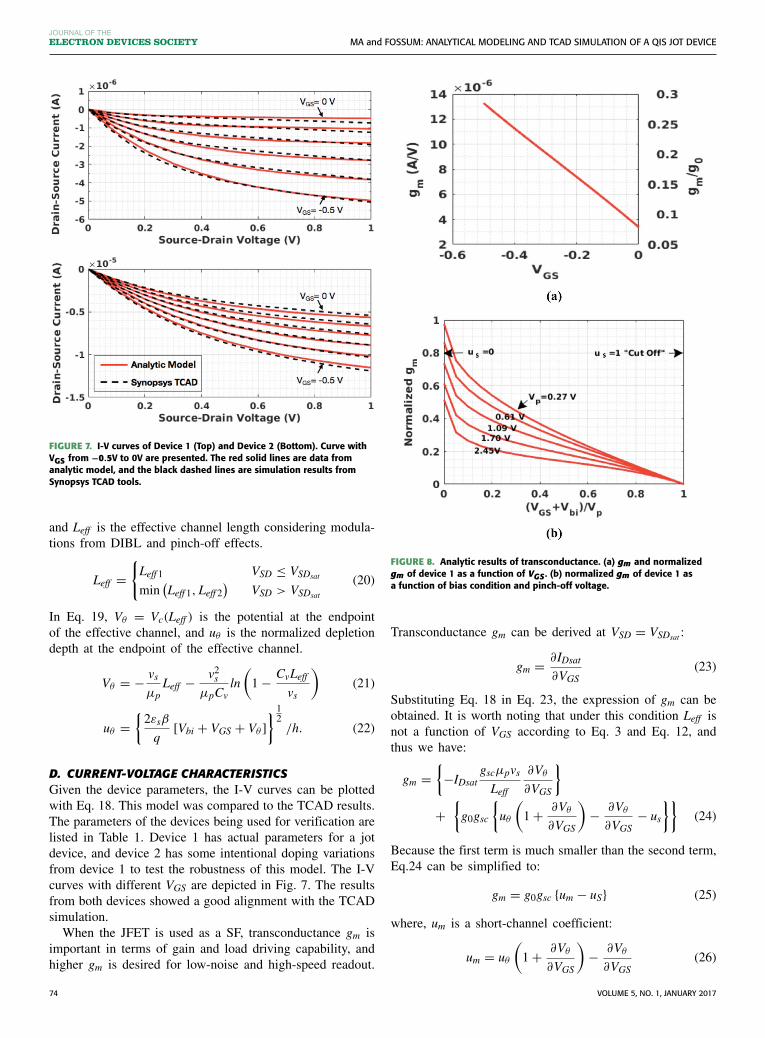
FIGURE 7. I-V curves of Device 1 (Top) and Device 2 (Bottom). Curve withVGS from −0.5V to 0V are presented. The red solid lines are data fromanalytic model, and the black dashed lines are simulation results fromSynopsys TCAD tools.
and Leff is the effective channel length considering modula-tions from DIBL and pinch-off effects.
Leff ={Leff1 VSD ≤ VSDsatmin
(Leff1,Leff2
)VSD > VSDsat
(20)
In Eq. 19, Vθ = Vc(Leff ) is the potential at the endpointof the effective channel, and uθ is the normalized depletiondepth at the endpoint of the effective channel.
Vθ = − vsμp
Leff − v2s
μpCvln
(1 − CvLeff
vs
)(21)
uθ ={
2εsβ
q[Vbi + VGS + Vθ ]
} 12
/h. (22)
D. CURRENT-VOLTAGE CHARACTERISTICSGiven the device parameters, the I-V curves can be plottedwith Eq. 18. This model was compared to the TCAD results.The parameters of the devices being used for verification arelisted in Table 1. Device 1 has actual parameters for a jotdevice, and device 2 has some intentional doping variationsfrom device 1 to test the robustness of this model. The I-Vcurves with different VGS are depicted in Fig. 7. The resultsfrom both devices showed a good alignment with the TCADsimulation.When the JFET is used as a SF, transconductance gm is
important in terms of gain and load driving capability, andhigher gm is desired for low-noise and high-speed readout.
FIGURE 8. Analytic results of transconductance. (a) gm and normalizedgm of device 1 as a function of VGS . (b) normalized gm of device 1 asa function of bias condition and pinch-off voltage.
Transconductance gm can be derived at VSD = VSDsat :
gm = ∂IDsat∂VGS
(23)
Substituting Eq. 18 in Eq. 23, the expression of gm can beobtained. It is worth noting that under this condition Leff isnot a function of VGS according to Eq. 3 and Eq. 12, andthus we have:
gm ={−IDsat gscμpvs
Leff
∂Vθ
∂VGS
}
+{g0gsc
{uθ
(1 + ∂Vθ
∂VGS
)− ∂Vθ
∂VGS− us
}}(24)
Because the first term is much smaller than the second term,Eq.24 can be simplified to:
gm = g0gsc {um − uS} (25)
where, um is a short-channel coefficient:
um = uθ
(1 + ∂Vθ
∂VGS
)− ∂Vθ
∂VGS(26)
74 VOLUME 5, NO. 1, JANUARY 2017

MA and FOSSUM: ANALYTICAL MODELING AND TCAD SIMULATION OF A QIS JOT DEVICE
FIGURE 9. Short channel factors um and gsc with different channel lengthL and VGS .
the term ∂Vθ
∂VGScan be solved from Eq. 21:
∂Vθ
∂VGS= −
ln(
1 − CvLeffvs
)+ CvLeff
vs−CvLeffln
(1 − CvL
vs
)+ CvL
vs−CvL(27)
and Cv can be obtained from Eq. 16 with VSD = VSDsat. Thenormalized gm is given by,
gm
g0= gsc {um − uS} (28)
As depicted in Fig. 8(a), the normalized gm has a valuefrom 0 to 1 and is dependent on VGS. It suggests that gm ismainly determined by g0, and g0 is affected by the devicedimensional ratio Wh
L and the channel doping concentrationNa. With given device parameters, lower VGS is preferredfor higher gm. Short-channel factors um and gsc both tendto 1 as channel length increases, as shown in Fig. 9. Inlong-channel JFETs, Eq. 28 can be simplified to:
gm = g0 (1 − uS) = g0
⎡⎣1 −
(Vbigc + VGS
Vp
) 12
⎤⎦ (29)
which exactly matches the result in [26]. The unit transcon-ductance g0 of device 1 is 51.1μA/V , which is very close tothe unit transconductance of a PMOS SF (∼54μA/V) withthe same dimensions and under the same process, but lowerthan a NMOS SF with the same dimensions (∼179μA/V)mostly due to the lower mobility of holes compared to elec-trons. However, the current driving capability of device 1 asa SF is already high enough to meet the high-speed opera-tion requirements in QIS application based on our empiricaldata, so higher gm may not be needed.According to Eq. 3, a larger channel depth h or higher
doping factor β leads to higher pinch-off voltage Vp, whichweakens the control of the gate on the channel current. It ispresented as a lower normalized gm as depicted in Fig. 8(b).
E. DEVICE DESIGN DISCUSSIONThis JFET device works as a SF, so the parameters must bewell engineered to meet requirements from other componentsin the jot device. For instance, the bias voltages range is
determined by, ⎧⎨⎩Vg = VFDVS = VoutVD = 0
(30)
where the FD potential VFD is determined by,
VRST − (CG× FWC) ≤ VFD ≤ VRST (31)
and VRST is the FD potential after reset. As presented inEq. 3, to make the JFET SF work in saturation mode, thefollowing condition must be satisfied,
VRST − (CG× FWC) ≥ Vp − Vbi (32)
In a jot device with a conventional reset transistor, VRST isflexible and can be adjusted according to the working rangeof the JFET SF. In a device with punch-through reset, Vrst isnormally confined to a certain range, and the design of theJFET needs to accommodate these constraints, whereby Vpand Vbi have to be engineered accordingly to have enoughFWC. The maximum FWC is given by:
FWCmax = VRST − Vp + VbiCG
(33)
The source follows the FD potential, and the output rangeis determined by the bias current and the I-V characteristicsof the JFET.
IV. PUNCH-THROUGH RESETThe punch-through reset technique was proposed to improvereset speed [30], and used in [15] to reduce the parasiticcapacitance from the reset gate. In [15], for example, thepunch-through reset voltage was over 20V. One of the goalsin our design was to reduce the voltage required for reset.The punch-through reset process relies on the fringing
effect induced by a strong lateral electric field in a NPNjunction. As shown in Fig. 2, FD and RD are separated bya p-type region, which creates a potential barrier betweenthe two n-type regions. During the reset state, RD is biasedto a higher level VRDHI , e.g., VDD. In this case, the p-typeregion is fully depleted by RD, and the strong lateral elec-tric field between FD and RD forces the potential in thep-region to increase. As shown in Fig. 10(a), the potentialbarrier between FD and RD is reduced with increased VRD.Electrons start to flow from FD to RD once the potential bar-rier has been lowered, as depicted in Fig. 11(a). Meanwhile,FD is discharged and VFD increases until the RD-FD electricfield is too weak to maintain punch-through. The FD voltageafter the reset VRST depends on the bias VRDHI during thereset and the reset pulse duration. After the reset, bias VRDis reduced to VRDLO and the potential barrier VB is restoredto stop electron current, as shown in Fig. 10(b). During the“off” state, in order to have a solid barrier on both FD andRD ends, VRD needs to be equal to, or near VRST , as shownby the green curve in Fig. 10(b). The maximum potentialbarrier height depends on the doping in the p-type regionand its width. It is a tradeoff that a higher potential barrier
VOLUME 5, NO. 1, JANUARY 2017 75
MA and FOSSUM: ANALYTICAL MODELING AND TCAD SIMULATION OF A QIS JOT DEVICE
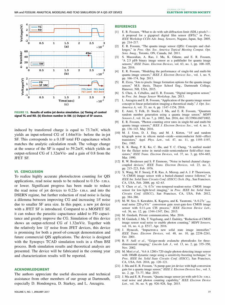
FIGURE 10. FD (left) to RD (right) electrostatic potential profile from TCADsimulation. Cutline is illustrated in Fig. 11. (a) Potential profile duringpunch-through reset with different VRD. VFD after reset changesaccordingly. (b) Potential profile after reset, with VFD = 1V . The height ofpotential barrier changes with different VRD.
FIGURE 11. FD (left) to RD (right) electron current density profile fromTCAD simulation. (a) Electron current density during punch-through resetwith VRD = 2.5V . (b) Electron current density after reset, with VRD = 1V .
after reset will also limit the highest reset voltage FD canreach during reset. In the case of device 1, FD can be resetto 1V with VRDHI of 3V, and after reset VB is about 0.9Vwith VRDLO of 1V. In this case, the barrier is strong enoughto stop electrons exchange between RD and FD, as depictedin Fig. 11(b). According to Eq. 33 the maximum FWC is824 e-, which is relatively small for conventional CIS, but
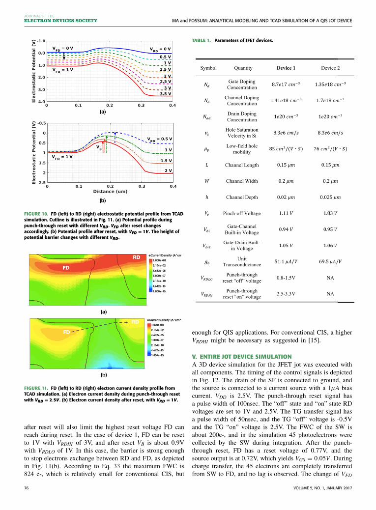
TABLE 1. Parameters of JFET devices.
enough for QIS applications. For conventional CIS, a higherVRDHI might be necessary as suggested in [15].
V. ENTIRE JOT DEVICE SIMULATIONA 3D device simulation for the JFET jot was executed withall components. The timing of the control signals is depictedin Fig. 12. The drain of the SF is connected to ground, andthe source is connected to a current source with a 1μA biascurrent. VDD is 2.5V. The punch-through reset signal hasa pulse width of 100nsec. The “off” state and “on” state RDvoltages are set to 1V and 2.5V. The TG transfer signal hasa pulse width of 50nsec, and the TG “off” voltage is -0.5Vand the TG “on” voltage is 2.5V. The FWC of the SW isabout 200e-, and in the simulation 45 photoelectrons werecollected by the SW during integration. After the punch-through reset, FD has a reset voltage of 0.77V, and thesource output is at 0.72V, which yields VGS = 0.05V . Duringcharge transfer, the 45 electrons are completely transferredfrom SW to FD, and no lag is observed. The change of VFD
76 VOLUME 5, NO. 1, JANUARY 2017
MA and FOSSUM: ANALYTICAL MODELING AND TCAD SIMULATION OF A QIS JOT DEVICE
FIGURE 12. Results of entire jot device simulation. (a) Timing of controlsignal TG and RD. (b) Electron number in SW. (c) Output of SF source.
induced by transferred charge is equal to 73.7mV, whichyields an input-referred CG of 1.64mV/e- before the in-jotSF. This corresponds to a 0.1fF total FD capacitance whichmatches the analytic calculation result. The voltage changeat the source of the SF is equal to 59.2mV, which yields anoutput-referred CG of 1.32mV/e- and a gain of 0.8 from theJFET SF.
VI. CONCLUSIONTo realize highly accurate photoelectron counting for QISapplications, read noise needs to be reduced to 0.15e- r.m.s.or lower. Significant progress has been made to reducethe read noise of jot devices to 0.22e- r.m.s. and into theDSERN regime, but further reduction of read noise is facinga dilemma between improving CG and increasing 1/f noisedue to smaller SF area size. In this paper, a new jot devicewith a JFET SF is introduced. Compared to a MOSFET SF,it can reduce the parasitic capacitance added to FD capaci-tance and greatly improve the CG. Simulation of this deviceshows an output-referred CG of 1.32mV/e. Together withthe relatively low 1/f noise from JFET devices, this deviceis promising for both a proof-of-concept demonstration andfuture commercial QIS applications. The device is designedwith the Synopsys TCAD simulation tools in a 45nm BSIprocess. Both simulation results and theoretical analysis arepresented. The device will be fabricated in the coming yearand characterization results will be reported.
ACKNOWLEDGMENTThe authors appreciate the useful discussion and technicalassistance from other members of our group at Dartmouth,especially D. Hondongwa, D. Starkey, and L. Anzagira.
REFERENCES[1] E. R. Fossum, “What to do with sub-diffraction-limit (SDL) pixels?—
A proposal for a gigapixel digital film sensor (DFS),” in Proc.IEEE Workshop CCDs Adv. Imag. Sensors, Nagano, Japan, Sep. 2005,pp. 214–217.
[2] E. R. Fossum, “The quanta image sensor (QIS): Concepts and chal-lenges,” in Proc. Opt. Soc. America Topical Meeting Comput. Opt.Sens. Imag., Toronto, ON, Canada, Jul. 2011.
[3] S. Masoodian, A. Rao, J. Ma, K. Odame, and E. R. Fossum,“A 2.5 pJ/b binary image sensor as a pathfinder for quanta imagesensors,” IEEE Trans. Electron Devices, vol. 63, no. 1, pp. 100–105,Jan. 2016.
[4] E. R. Fossum, “Modeling the performance of single-bit and multi-bitquanta image sensors,” IEEE J. Electron Devices Soc., vol. 1, no. 9,pp. 166–174, Sep. 2013.
[5] R. Zizza, “Jots to pixels: Image formation options for the quanta imagesensor,” M.S. thesis, Thayer School Eng., Dartmouth College,Hanover, NH, USA, 2015.
[6] S. Chen, A. Ceballos, and E. R. Fossum, “Digital integration sensor,”in Proc. Int. Image Sensor Workshop, Jun. 2013.
[7] L. Anzagira and E. R. Fossum, “Application of the quanta image sensorconcept to linear polarization imaging-a theoretical study,” J. Opt. Soc.America A, vol. 33, no. 6, pp. 1147–1154, 2016.
[8] E. Amri, Y. Felk, D. Stucki, J. Ma, and E. R. Fossum, “Quantumrandom number generation using a quanta image sensor,” MDPISensors J., vol. 16, no. 7, p. 1002, Jun. 2016, doi: 10.3390/s16071002.
[9] E. R. Fossum, “Photon counting error rates in single-bit and multi-bitquanta image sensors,” IEEE J. Electron Devices Soc., vol. 4, no. 3,pp. 136–143. May 2016.
[10] M. J. Uren, D. J. Day, and M. J. Kirton, “1/f and randomtelegraph noise in silicon metal−oxide−semiconductor field−effecttransistors,” Appl. Phys. Lett., vol. 47, no. 11, pp. 1195–1197,Dec. 1985.
[11] K. K. Hung, P. K. Ko, C. Hu, and Y. C. Cheng, “A unified modelfor the flicker noise in metal-oxide-semiconductor field-effect tran-sistors,” IEEE Trans. Electron Devices, vol. 37, no. 3, pp. 654–665,Mar. 1990.
[12] R. W. Brodersen and S. P. Emmons, “Noise in buried channel charge-coupled devices,” IEEE Trans. Electron Devices, vol. 23, no. 2,pp. 215–223, Feb. 1976.
[13] X. Wang, M. F. Snoeij, P. R. Rao, A. Mierop, and A. J. P. Theuwissen,“A CMOS image sensor with a buried-channel source follower,” inIEEE Int. Solid State Circuits Conf. (ISSCC) Tech. Dig., San Francisco,CA, USA, Feb. 2008, pp. 62–63.
[14] Y. Chen et al., “A 0.7e− rms-temporal-readout-noise CMOS imagesensor for low-light-level imaging,” in Proc. IEEE Int. Solid StateCircuits Conf. (ISSCC), San Francisco, CA, USA, Feb. 2012,pp. 384–386.
[15] M.-W. Seo, S. Kawahito, K. Kagawa, and K. Yasutomi, “A 0.27e−rmsread noise 220-μV/e− conversion gain reset-gate-less CMOS imagesensor with 0.11-μm CIS process,” IEEE Electron Device Lett.,vol. 36, no. 12, pp. 1344–1347, Dec. 2015.
[16] M. Guidash, Private communication, Mar. 2016.[17] M. Guidash, J. Ma, T. Vogelsang, and J. Endsley, “Reduction of CMOS
image sensor read noise to enable photon counting,” MDPI Sensors,vol. 16, no. 4, p. E517, Apr. 2016.
[18] J. Hynecek, “Impactron-a new solid state image intensifier,”IEEE Trans. Electron Devices, vol. 48, no. 10, pp. 2238–2241,Oct. 2001.
[19] B. F. Aull et al., “Geiger-mode avalanche photodiodes for three-dimensional imaging,” Lincoln Lab. J., vol. 13, no. 2, pp. 335–350,Nov. 2002.
[20] M. Mori et al., “6.6 A 1280×720 single-photon-detecting image sensorwith 100dB dynamic range using a sensitivity-boosting technique,” inProc. IEEE Int. Solid State Circuits Conf. (ISSCC), San Francisco,CA, USA, Feb. 2016, pp. 120–121.
[21] J. Ma and E. R. Fossum, “A pump-gate jot device with high conversiongain for a quanta image sensor,” IEEE J. Electron Devices Soc., vol. 3,no. 2, pp. 73–77, Mar. 2015.
[22] J. Ma and E. R. Fossum, “Quanta image sensor jot with sub 0.3e- r.m.s.read noise and photon counting capability,” IEEE Electron DeviceLett., vol. 36, no. 9, pp. 926–928, Sep. 2015.
VOLUME 5, NO. 1, JANUARY 2017 77

MA and FOSSUM: ANALYTICAL MODELING AND TCAD SIMULATION OF A QIS JOT DEVICE
[23] J. Ma, D. Starkey, A. Rao, K. Odame, and E. R. Fossum,“Characterization of quanta image sensor pump-gate jots with deepsub-electron read noise,” IEEE J. Electron Devices Soc., vol. 3, no. 6,pp. 472–480, Nov. 2015.
[24] J. Hynecek, “Vertical JFET source follower for small pixel CMOSimage sensors,” U.S. Patent 8 937 272 B2, Jan. 20, 2015.
[25] H. Nomura, T. Shima, A. Kamashita, T. Ishida, and T. Yoneyama,“A 256/spl times/256 BCAST motion detector with simultaneous videooutput,” in IEEE Int. Solid State Circuits Conf. (ISSCC) Tech. Dig.,San Francisco, CA, USA, Feb. 1998, pp. 282–283.
[26] S. M. Sze, “JFET and MESFET,” in Physics of Semiconductor Devices,2nd ed. New York, NY, USA: Wiley, 1981, ch. 6, pp. 312–362.
[27] U. K. Mishra and J. Singh, “Field effect transistors,” in SemiconductorDevice Physics and Design, 1st ed. Dordrecht, The Netherlands:Springer, 2008, ch. 8, pp. 356–432.
[28] J. Chang, A. K. Kapoor, L. F. Register, and S. K. Banerjee, “Analyticalmodel of short-channel double-gate JFETs,” IEEE Trans. ElectronDevices, vol. 57, no. 8, pp. 1846–1855, Aug. 2010.
[29] Y. Hu, R. V. H. Booth, and M. V. White, “An analytical model for thelateral channel electric field in LDD structures,” IEEE Trans. ElectronDevices., vol. 37, no. 10, pp. 2254–2264, Oct. 1990.
[30] R. M. Guidash, “Solid state image sensor with fast reset,” U.S.Patent 5 338 946 A, Aug. 16, 1994.
JIAJU MA (S’12) received the B.S. degree inphysics from Nankai University, China, in 2012.He is currently pursuing the Ph.D. degree withthe Thayer School of Engineering at Dartmouth.He is exploring low-noise CMOS image sensorpixel devices for quanta image sensor and otherphoton-counting imaging applications.
ERIC R. FOSSUM (S’80–M’84–SM’91–F’98) iscurrently a Professor with the Thayer Schoolof Engineering, Dartmouth. He is the PrimaryInventor of the CMOS image sensor used in bil-lions of camera phones and other applications. Hewas inducted into the National Inventors Hall ofFame and a member of the National Academyof Engineering. He is the Co-Founder and thePast President of the International Image SensorSociety and the Director of the National Academyof Inventors. He is currently exploring the quantaimage sensor.
78 VOLUME 5, NO. 1, JANUARY 2017