TCAD Modeling for Mechanical Stress Management in … · TCAD Modeling for Mechanical Stress...
20
© 2014 Synopsys, Inc. All rights reserved. 1 TCAD Modeling for Mechanical Stress Management in 3D IC Packages Xiaopeng Xu TCAD R&D, Synopsys Mountain View, California June 12, 2014 NCCAVS Joint User Group Meeting on 3D Packaging
Transcript of TCAD Modeling for Mechanical Stress Management in … · TCAD Modeling for Mechanical Stress...

© 2014 Synopsys, Inc. All rights reserved. 1
TCAD Modeling for Mechanical
Stress Management in 3D IC Packages
Xiaopeng Xu
TCAD R&D, Synopsys Mountain View, California
June 12, 2014
NCCAVS Joint User Group Meeting on 3D Packaging
© 2014 Synopsys, Inc. All rights reserved. 2
Outline
• Thermal Mismatch Stresses in 3D IC
• Modeling stress evolution with TCAD
• Analyzing stress effects on performance and
reliability
• Stress management in 3D IC technology
integration and design

© 2014 Synopsys, Inc. All rights reserved. 3
Through Silicon Via Stress Effects
Via material,
process
Barrier layer
material
Insulation liner
material and
thickness
TSV pitch,
diameter
• Mobility change
- Radial tension
- Circumferential
compression
Pumping
• Reliability
Performance shifting due to TSV stress
- IMEC, VLSI 2010
Silicon crystal
orientation, P/N
TSV extrusion and de-lamination
- Tezzaron, RTI 2009
Synopsys, Chip Scale Review, April 2014
IMEC

© 2014 Synopsys, Inc. All rights reserved. 4
Thermal Mismatch Stress near u-bump
Active
region
Thermal mismatch leads to die
pull-down and bump push-up
Micro-bump Array
Top Die
Bottom
Die
Micro-bumps
Smear
Smear Under-fill Oxide
Oxide
Deformed Micro-bump
bumpfillunder
Synopsys, MRS Proceedings, 2011

© 2014 Synopsys, Inc. All rights reserved. 5
Micro-bump Stress Effects
• Micro-bumps introduce stresses that depend on
Micro-bump and under-fill material properties
Micro-bump geometry and layout parameters
• Micro-bump stress effects
Current shift in devices above micro bumps
Interface delamination and cracking
IME, EPTC 2009 IMEC, ECTC 2011
Interface cracking
near micro-bump
Device On current shift
above micro-bump
Synopsys, MRS Proceedings, 2011

© 2014 Synopsys, Inc. All rights reserved. 6
Outline
• Thermal Mismatch Stresses in 3D IC
• Modeling stress evolution with TCAD
• Analyzing stress effects on performance
and reliability
• Stress management in 3D IC technology
integration and design

© 2014 Synopsys, Inc. All rights reserved. 7
TCAD 3D IC Simulation Flow
Deposit material=Oxide thickness=0.3 type=isotropic
Etch mask=metal_2 material=Oxide thickness=0.3
Layout Info
3D Structures
Solution Fields
Mobility Variations
Reliability Analyses
Process Info
Process Simulation
Finite Element Analysis
Reliability
Effective
Stress
Mobility Variation
IMEC/Synopsys et al, IEDM 2010 Synopsys, IRPS 2009
Material Property Model Selection
Synopsys, AIP Conference Proceedings, Vol. 1378, 2011

© 2014 Synopsys, Inc. All rights reserved. 8
Bottom die
(Die 1)
TSV
Bottom die
(Die 1) BEOL
RDL
Oxide
TSV
Micro-bump Top die
(Die 2)
Bottom die
(Die 1) BEOL
BEOL Under-fill
RDL
Oxide
RDL
Oxide
TSV
Micro-bump
FEOL TSV BEOL Thinning Backside m-Bump Stacking
BEOL
Die 1
Die 2
1 2 3
TSV and m-bump Stress Simulation
After TSV step
After stacking step After bump step
Layout
Via-middle process:
Synopsys, 12th Int. Workshop on Stress in Microelectronics, 2012

© 2014 Synopsys, Inc. All rights reserved. 9
Stress Evolution with Process Steps
Sxx (Pa)
After TSV step After micro-bump step
100 MPa Die 1
Die 1
TSV TSV
100 MPa
Synopsys, 12th Int. Workshop on Stress in Microelectronics, 2012
© 2014 Synopsys, Inc. All rights reserved. 10
Top die
(Die 2)
Bottom die
(Die 1)BEOL
BEOLUnder-fill
RDL
Oxide
RDL
OxideTSV
Micro-bump
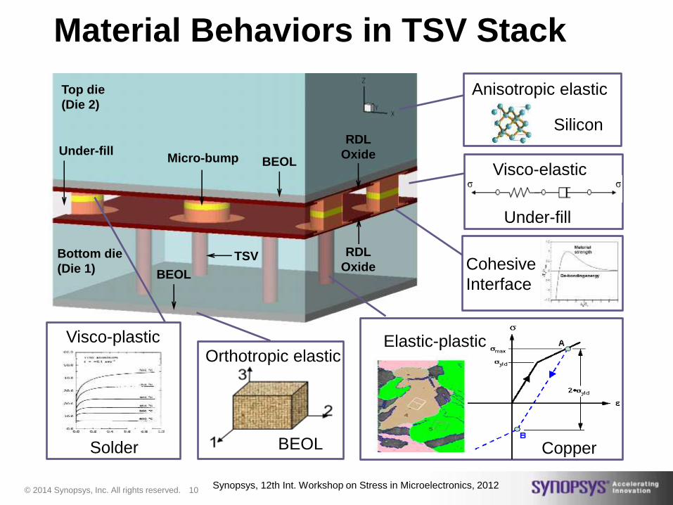
Material Behaviors in TSV Stack
Anisotropic elastic
Silicon
Visco-elastic
Under-fill
Elastic-plastic
Copper
Orthotropic elastic
BEOL
Visco-plastic
Solder
Cohesive
Interface
Synopsys, 12th Int. Workshop on Stress in Microelectronics, 2012

© 2014 Synopsys, Inc. All rights reserved. 11
Outline
• Thermal Mismatch Stresses in 3D IC
• Modeling stress evolution with TCAD
• Analyzing stress effects on performance
and reliability
• Stress management in 3D IC technology
integration and design

© 2014 Synopsys, Inc. All rights reserved. 12
P-mobility Variation on Die-1 Surface
TSV
(%)
[001]/[110]
5%
- 5%
Top die
(Die 2)
Bottom die
(Die 1)BEOL
BEOLUnder-fill
RDL
Oxide
RDL
OxideTSV
Micro-bump
• Mobility variation localized around TSVs
• Keep-Out-Zone (KOZ) design rule and place & route methodology
Stress around TSV - Radial tension
- Circumferential compression
Synopsys, 12th international workshop on stress-induced phenomena in microelectronics, 2012

© 2014 Synopsys, Inc. All rights reserved. 13
TSV Diameter and Pitch Effects
TSV Diameter = 5 um TSV Diameter = 10 um
~38% higher normal stress
Synopsys, 12th international workshop on stress-induced phenomena in microelectronics, 2012

© 2014 Synopsys, Inc. All rights reserved. 14
N-mobility Variation on Die-2 Surface
(%)
Top Die
Bottom Die
Micro-bumps
BEOL
BEOLUnder-fillRDL
Oxide
RDLOxide
• Mobility variation localized above u-bump
• KOZ design rule and place & route methodology
Active
region
Synopsys, 12th international workshop on stress-induced phenomena in microelectronics, 2012

© 2014 Synopsys, Inc. All rights reserved. 15
Under-fill CTE Impact LCTE: 15.0, 30.0 and 45.0 ppm/C
Larger under-fill CTE leads to greater mobility variation
Active region
Large under-fill CTE
increases contraction
and pulling down
Synopsys, MRS Proceedings, 2011
-5
0
5
10
15
20
0 5 10 15 20 25
N-M
obil
ity
chan
ge [
%]
Distance along x-axis [mm]
15 ppm/ C, N-mob
30 ppm/ C, N-mob
45 ppm/ C, N-mob
-5
0
5
10
15
20
0 5 10 15 20 25
N-M
obil
ity
chan
ge [
%]
Distance along x-axis [mm]
15 ppm/ C, N-mob
30 ppm/ C, N-mob
45 ppm/ C, N-mob
Under-fill CTE
Above
Bump

© 2014 Synopsys, Inc. All rights reserved. 16
Copper Anisotropic Effect on Crack
Isotropic Anisotropic 1 Anisotropic 2 (Pa)
Anisotropic Copper E1 E2 E3
Anisotropic 1 156 GPa 69 GPa 69 GPa
Anisotropic 3 69 GPa 69 GPa 156 GPa
• Crack driving force and mode mixity
depends on copper anisotropy in
different crystal orientation
TSV Si
BEOL
Top die
(Die 2)
Bottom die
(Die 1)BEOL
BEOLUnder-fill
RDL
Oxide
RDL
OxideTSV
Micro-bump
TSV Si
BEOL
TSV Si
BEOL
Synopsys/Fraunhofer, IEEE TDMR, 2012

© 2014 Synopsys, Inc. All rights reserved. 17
Outline
• Thermal Mismatch Stresses in 3D IC
• Modeling stress evolution with TCAD
• Analyzing stress effects on performance
and reliability
• Stress management in 3D IC technology
integration and design

© 2014 Synopsys, Inc. All rights reserved. 18
Managing KOZ with TCAD Modeling
M. Rabie, et al, GLOBAL FOUNDRIES, IITC 2014
• Tensile stress due to TSV copper shrinkage is compensated by
compressive stress due to CMP stop layer
• Experiments and TCAD simulations

© 2014 Synopsys, Inc. All rights reserved. 19
Stress Management at Qualcomm
TSV Effect m-Bump Effect Stacking Effect
Qualcomm, CICC 2010, ECTC 2014
TSV
+ ve
- ve
change
Active
Pocke Active
Pockets
Mobility Change
Layout
View

© 2014 Synopsys, Inc. All rights reserved. 20
Summary
• Mechanical stress in TSV stacks affects both performance and reliability
• TCAD modeling of stress evolution and stress effects provides valuable insights
• 3D IC design and technology configurations can be optimized with stress management