17 May 2011Matthias Bergholz DESY Zeuthen 1 Simulations with TCAD Tutorial.

18/01/2021
TCAD+APSQ SIMULATIONS FOR
CLICTDKatharina Dort
Vertex and Tracker Meeting
2
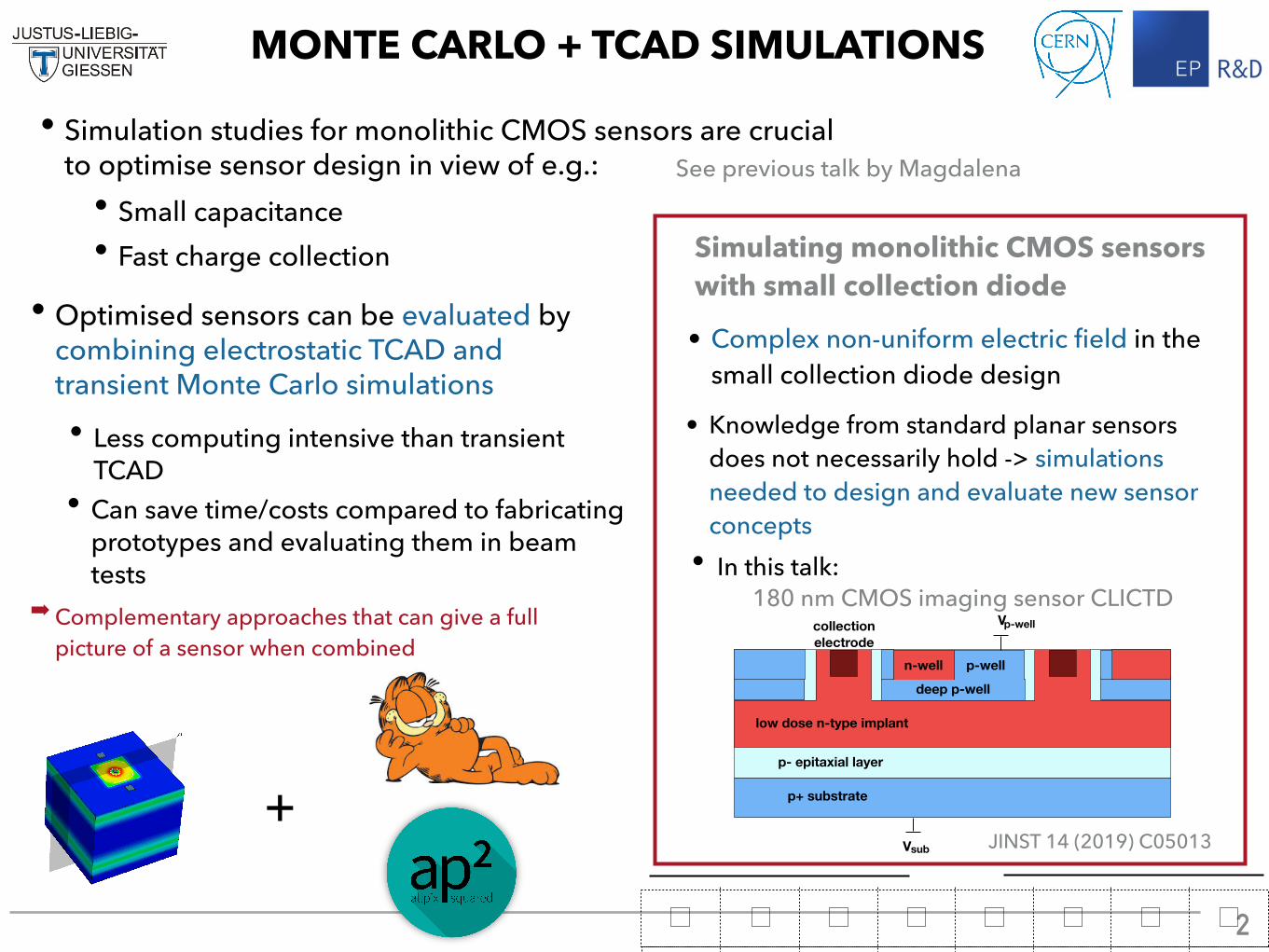
MONTE CARLO + TCAD SIMULATIONS
collection electrode
n-implant37.5 μm
30 μ
m
300 μm
collection electrode
low dose n-type implant
p- epitaxial layer
p+ substrate
n-well p-well
deep p-well
Vp-well
Vsub
column
row
• In this talk:
• Complex non-uniform electric field in the small collection diode design
Simulating monolithic CMOS sensors with small collection diode
• Simulation studies for monolithic CMOS sensors are crucial to optimise sensor design in view of e.g.:
• Small capacitance • Fast charge collection
See previous talk by Magdalena
• Optimised sensors can be evaluated by combining electrostatic TCAD and transient Monte Carlo simulations • Less computing intensive than transient
TCAD
+
• Knowledge from standard planar sensors does not necessarily hold -> simulations needed to design and evaluate new sensor concepts
180 nm CMOS imaging sensor CLICTD
JINST 14 (2019) C05013
➡ Complementary approaches that can give a full picture of a sensor when combined
• Can save time/costs compared to fabricating prototypes and evaluating them in beam tests

3
ALLPIX SQUARED + TCAD SIMULATIONS
• Validation of simulation with Investigator test-chip (developed within ALICE ITS upgrade)
NIM A 964 (2020) 163784
Paul Schütze, Simon Spannagel | Allpix Squared – Status and Plans | 16 December 2020 4
Particle Detection in Silicon Sensors
SignalTransfer
DigitizationChargeTransport
EnergyDeposition
incidentradiation
e-e-
e-
e-
e-
e-
e-e-
e-
h
hhh
hAC/DC 0111010010100101
detectorreadout
x
t
hhh
h
h
Stage 1 Stage 2 Stage 3
e-
Stage 4
https://cern.ch/allpix-squared/
Please see e.g. https://indico.cern.ch/event/984049/
• Allpix Squared handles all simulation steps from charge deposition in sensor to digitisation of signal
• Static fields are imported from 3D TCAD simulations to ensure precise field modelling All 3D TCAD simulations in this talk were performed by M. Munker
NIM A 901 (2018) 164-172
From Paul’s and Simon’s talk in the monolithic sensor simulation meeting
4
ALLPIX SQUARED + TCAD SIMULATIONS
The charge carrier transport is mainly dominated by the436
precision of the numeric integration and its granularity.437
The number of charge carriers transported as group has438
been varied from a single charge carrier up to ten per group439
in order to study possible e↵ects on the distribution at the440
implants. The e↵ect on the reconstruction observables is441
found to be negligible.442
Parameters constrained by measurements. The behavior443
of the sensor has been shown to be very sensitive to the444
simulated physical properties of the CMOS sensor, i.e. the445
thickness of the epitaxial layer as well as the modeled elec-446
tric field. Even small changes in the sensor design, such447
as a more simplistic approximation of the implant dop-448
ing profiles in the TCAD design cause large changes in449
the resulting cluster size distributions and position resolu-450
tion. It is therefore of paramount importance to model the451
sensor as precisely as possible and to constrain the di↵er-452
ent parameters in TCAD by additional measurements [22].453
The low-field regions found in the corners of the pixel cell454
visible in Figures 3 and 4 are strongly influenced by these455
modifications, and their contribution to the detector signal456
changes accordingly.457
The integration time currently used to stop the trans-458
port of charge carriers is also linked to the sensor design,459
since it is used to emulate an e↵ective recombination of460
charge carriers. Their lifetime in the di↵erent regions of461
the sensor is dominated by the respective doping concen-462
tration, and potentially a↵ected by the silicon wafer pro-463
duction process. Since this was not modeled in detail for464
this simulation, the integration time was chosen such that465
the MPV of the cluster charge matched the value obtained466
from data as discussed in Section 4. The corresponding467
uncertainty on the charge calibration of the reference data468
has therefore to be taken into account as systematic uncer-469
tainty of the simulation by comparing the cluster charge470
MPV for di↵erent integration times to the value obtained471
from data as shown in Figure 8. Here, the hatched band472
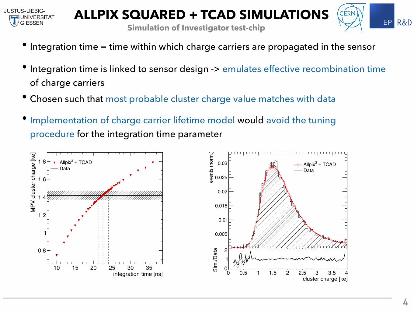
integration time [ns]10 15 20 25 30 35
MPV
clu
ster
cha
rge
[ke]
0.8
1
1.2
1.4
1.6
1.8 + TCAD2AllpixData
Figure 8: Most probable cluster charge as a function of the simu-
lated integration time. The black horizontal line represents the value
obtained from data, the hatched band corresponds to the assumed
systematic uncertainty of the charge calibration.
represents an assumed uncertainty of ±50 e on the charge473
calibration of data [7, 9]. This translates to an uncertainty474
on the integration time of 22.5+1.5�1.3 ns, which is propagated475
as systematic uncertainty to the results presented in this476
paper.477
It has been observed that the overall agreement between478
data and simulation seems to improve for lower integration479
times, which might indicate either an o↵set in the absolute480
charge calibration of data or an insu�cient modeling of the481
signal formation processes in silicon.482
Also the charge threshold applied to the individual pix-483
els has a strong impact on both the cluster size and the in-484
trinsic resolution, with decreasing influence towards higher485
thresholds. At a threshold of 40 e, a change of as little486
as ±5 e visibly alters the observables. Since the absolute487
charge calibration and the threshold value in electrons are488
fully correlated, the uncertainty on the applied threshold489
has been taken into account by varying the two parameters490
simultaneously and by calculating the total uncertainty491
arising from the variations.492
10
A variation of the threshold dispersion and electronics493
noise of up to 10 e at a threshold of 40 e yielded no observ-494
able e↵ect. The values for noise and threshold dispersion495
have been estimated from the evaluation of the full wave-496
form in data [9].497
The residual width and the final intrinsic resolution de-498
pend on the resolution of the reference tracks at the po-499
sition of the detector under investigation. This resolution500
has been determined for the test-beam data used, and a501
variation of ±0.2 µm around this value shifts the obtained502
resolution accordingly. This strong influence arises from503
the fact that the two values are of similar size.504
In summary, while the free parameters of the simulation505
have little to no influence on the final result when varied506
within a reasonable range, several parameters show a high507
sensitivity but are constrained by measurements.508
7. Validation With Test-Beam Data509
The simulation is compared to data recorded with the510
Investigator chip, described in Section 3, at the CERN511
SPS accelerator with a 120GeV ⇡+ beam. A total of512
25660 tracks through the region of interest have been513
recorded, mainly limited by the very small active area of514
the DUT and the dead time of the data acquisition system515
used. More details about the test-beam setup, data sam-516
ples and the analysis of data used for comparison in this517
paper can be found in [6, 9].518
7.1. Cluster Charge519
The cluster charge distributions for both simulation and520
data at a charge threshold of 120 e are shown in Figure 9.521
The distributions are fitted with the convolution of a Gaus-522
sian and Landau function. The MPV is 1.42 ke for both523
data and simulation, and the width of the Gaussian is524
0.21 ke/0.22 ke for data/simulation, respectively. A good525
agreement between data and simulation is observed, as526
also indicated by the ratio of the two distributions dis-527
played in the lower part of the figure. While the MPV528
cluster charge [ke]0 0.5 1 1.5 2 2.5 3 3.5 4Si
m./D
ata
012
cluster charge [ke]
eve
nts
(nor
m.)
0.005
0.01
0.015
0.02
0.025
0.03 + TCAD2AllpixData
Figure 9: Cluster charge distributions at a pixel threshold of 120 e for
simulation and experiment. The distributions resemble the expected
Landau-Gauss distribution. The hatched band represents the total
uncertainty.
has been tuned to match data using the integration time529
of the simulation as discussed in Section 4, the agreement530
of the shapes indicates that the energy deposition in the531
relevant parts of the sensor as well as the collection of532
charge carriers is well-modeled by the simulation. The533
data distribution exhibits some fluctuations owing to the534
low statistics of the sample.535
7.2. Cluster Size536
The distribution of the total cluster size at a thresh-537
old of 120 e for simulation and experiment is presented538
in Figure 10. Qualitatively, the distributions are in good539
agreement. A possible source of the observed deviations540
for individual cluster sizes are uncertainties in the modeled541
electric field of the sensor as discussed in Section 6.542
The projection of the cluster size in x and y, depicted543
in Figure 11, provides additional details about the charge544
sharing process. Data and simulation agree well, but a545
small di↵erence between the distributions in x and y can546
be observed in data despite the symmetry of the pixel cell547
11
• Integration time = time within which charge carriers are propagated in the sensor
• Integration time is linked to sensor design -> emulates effective recombination time of charge carriers
• Chosen such that most probable cluster charge value matches with data
• Implementation of charge carrier lifetime model would avoid the tuning procedure for the integration time parameter
Simulation of Investigator test-chip

5
CHARGE CARRIER RECOMBINATION
Solar Energy 76 (2004) 255–262
1τeff
=1
τSRH+
1τAuger
0 5 10 15 20 25 300.015−
0.01−
0.005−
0
0.005
0.01
0.015
1
10
210
310
410
510
recomb_map_
# Recombinations
Y [um]
Z [m
m]
• Charge carrier recombination was implemented based on the following models:
• Shockley-Read-Hall (SRH) recombination
• Auger recombination
• Effective charge carrier lifetime:
• Effective lifetime in highly doped bulk : a few nanoseconds
(doping-dependent)
(doping-dependent)
6
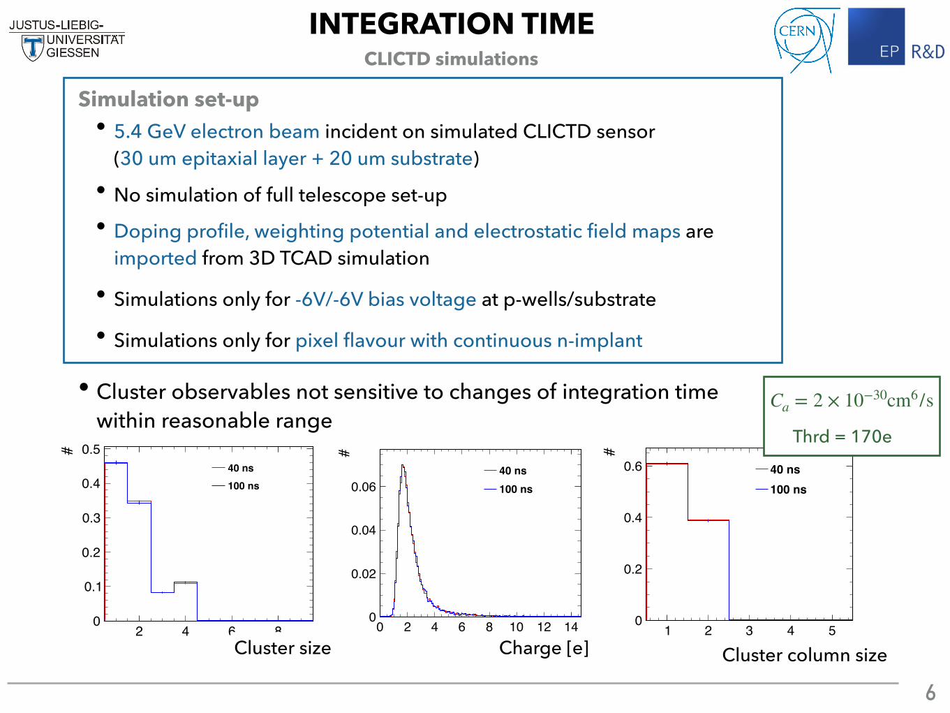
INTEGRATION TIME
2 4 6 8size
0
0.1
0.2
0.3
0.4
0.5#
40 ns
100 ns
0 2 4 6 8 10 12 14charge [e]
0
0.02
0.04
0.06
#
40 ns
100 ns
1 2 3 4 5size in x
0
0.2
0.4
0.6
#
40 ns100 ns
• Cluster observables not sensitive to changes of integration time within reasonable range
Cluster size Cluster column sizeCharge [e]
Simulation set-up• 5.4 GeV electron beam incident on simulated CLICTD sensor
(30 um epitaxial layer + 20 um substrate)
• Doping profile, weighting potential and electrostatic field maps are imported from 3D TCAD simulation
• Simulations only for -6V/-6V bias voltage at p-wells/substrate
• Simulations only for pixel flavour with continuous n-implant
• No simulation of full telescope set-up
CLICTD simulations
Thrd = 170e
Ca = 2 × 10⁻³⁰cm6/s

7
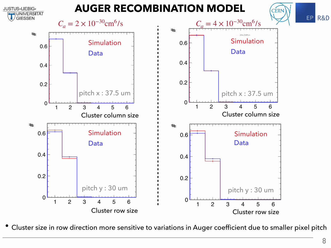
AUGER RECOMBINATION MODEL
2 4 6size
0
0.1
0.2
0.3
0.4
0.5#
simulation
data
2 4 6 8size
0
0.1
0.2
0.3
0.4
0.5
#
simulation
data
• Lifetime for Auger recombination: τAuger =1
Ca ⋅ n2
Ca = 4 × 10⁻³⁰cm6/sCa = 2 × 10⁻³⁰cm6/s
How sensitive are cluster observables to variations of the parameters in the lifetime models?
• Increasing Auger coefficient is expected to lead to a lower effective lifetime and therefore a decrease in cluster size
SimulationData
SimulationData
Thrd = 170e
Cluster size Cluster size
• Minor impact on cluster size at a threshold of 170e
8
1 2 3 4 5 6size in x
0
0.2
0.4
0.6
#
simulation
data
1 2 3 4 5 6size in x
0
0.2
0.4
0.6
#simulation
data
AUGER RECOMBINATION MODEL
1 2 3 4 5 6size in y
0
0.2
0.4
0.6
#
simulation
data
1 2 3 4 5 6size in y
0
0.2
0.4
0.6
#
simulation
data
Ca = 4 × 10⁻³⁰cm6/sCa = 2 × 10⁻³⁰cm6/s
SimulationData
SimulationData
SimulationData
SimulationData
• Cluster size in row direction more sensitive to variations in Auger coefficient due to smaller pixel pitch
pitch y : 30 um pitch y : 30 um
pitch x : 37.5 umpitch x : 37.5 um
Cluster column size Cluster size in x
Cluster row size
Cluster column size
Cluster row size
9
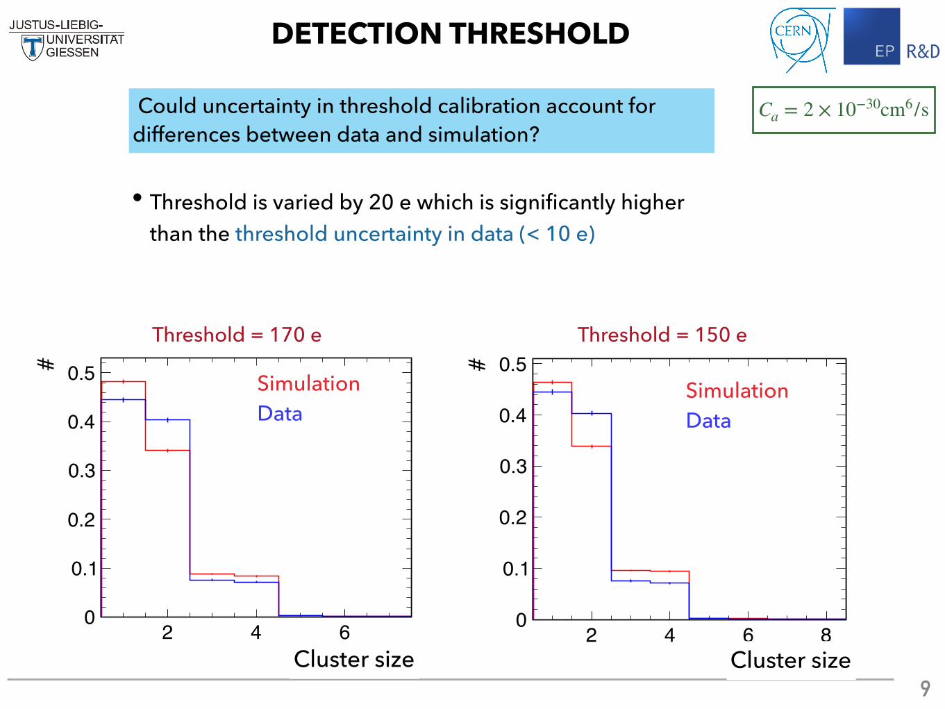
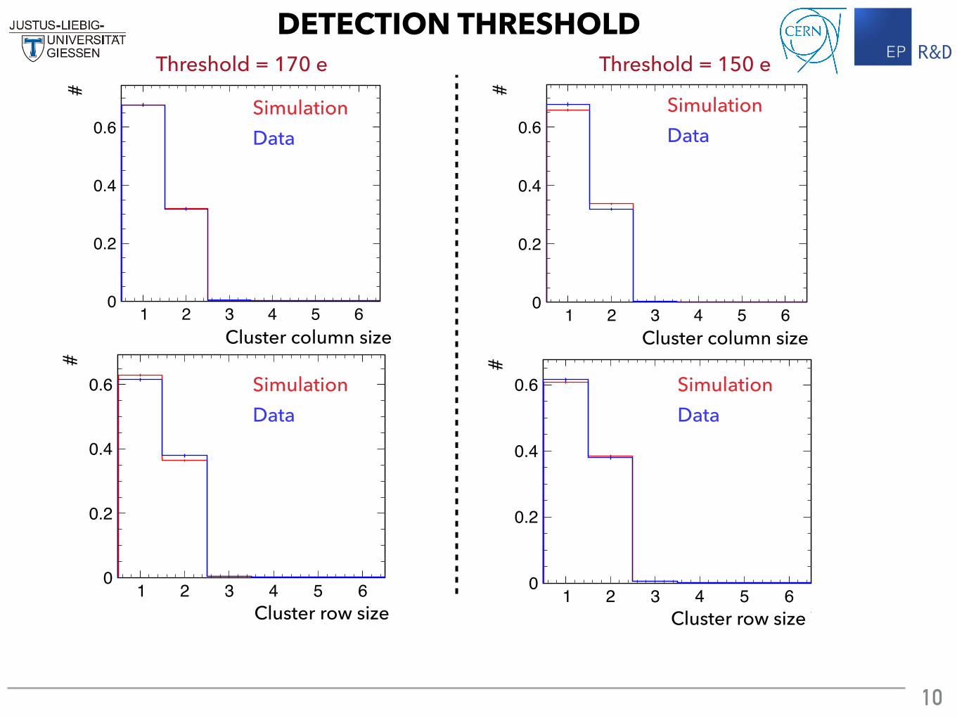
DETECTION THRESHOLD
2 4 6size
0
0.1
0.2
0.3
0.4
0.5#
simulation
data
2 4 6 8size
0
0.1
0.2
0.3
0.4
0.5#
simulation
data
Threshold = 170 e Threshold = 150 e
Ca = 2 × 10⁻³⁰cm6/s Could uncertainty in threshold calibration account for differences between data and simulation?
Cluster size Cluster size
SimulationData
SimulationData
• Threshold is varied by 20 e which is significantly higher than the threshold uncertainty in data (< 10 e)
10
1 2 3 4 5 6size in x
0
0.2
0.4
0.6
#simulation
data
1 2 3 4 5 6size in x
0
0.2
0.4
0.6
#
simulation
data
Threshold = 170 e Threshold = 150 e
1 2 3 4 5 6size in y
0
0.2
0.4
0.6
#
simulation
data
1 2 3 4 5 6size in y
0
0.2
0.4
0.6
#
simulation
data
DETECTION THRESHOLD
SimulationData
SimulationData
SimulationData
SimulationData
Cluster column size
Cluster row size
Cluster column size
Cluster row size
11
LATERAL PROFILE SPREAD OF P-WELL IMPLANT
10− 0 10m]µin-pixel y [
15−
10−
5−
0
5
10
15
m]
µin
-pix
el z
[
10−8−6−4−2−
0246
6−10×
ele
ctric
fiel
d y
diffe
renc
e
CLICdp work in progress
collection electrode
n-implant37.5 μm
30 μ
m
300 μm
collection electrode
low dose n-type implant
p- epitaxial layer
p+ substrate
n-well p-well
deep p-well
Vp-well
Vsub
column
row
What is the impact of uncertainties in the doping profiles on the charge sharing ?
• Lateral spread of the profile at the edge of the p-well implant (p-well smearing) was varied
Low p-well smearing - high p-well smearingDifferences in electric field in y
• Low smearing leads to a stronger lateral electric field
Collection diode
12
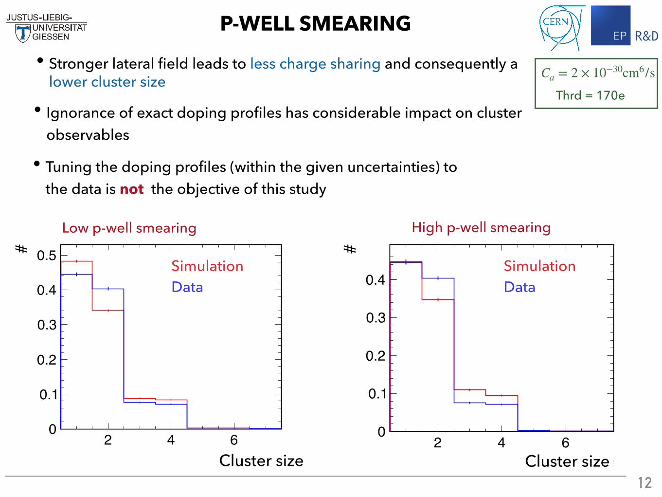
P-WELL SMEARING
Low p-well smearing
2 4 6size
0
0.1
0.2
0.3
0.4
0.5#
simulation
data
2 4 6size
0
0.1
0.2
0.3
0.4
#
simulation
data
• Ignorance of exact doping profiles has considerable impact on cluster observables
• Stronger lateral field leads to less charge sharing and consequently a lower cluster size
• Tuning the doping profiles (within the given uncertainties) to the data is not the objective of this study
Ca = 2 × 10⁻³⁰cm6/sThrd = 170e
High p-well smearing
Cluster size Cluster size
SimulationData
SimulationData

13
P-WELL SMEARING
1 2 3 4 5 6size in x
0
0.2
0.4
0.6
#simulation
data
2 4 6size in x
0
0.2
0.4
0.6
#
simulation
data
1 2 3 4 5 6size in y
0
0.2
0.4
0.6
#
simulation
data
2 4 6size in y
0
0.2
0.4
0.6
#
simulation
data
Low p-well smearing High p-well smearing
• Effect of p-well smearing is clearly visible in both spatial dimensions
Cluster column size
Cluster row size
Cluster column size
Cluster row size
SimulationData
SimulationData
SimulationData
SimulationData
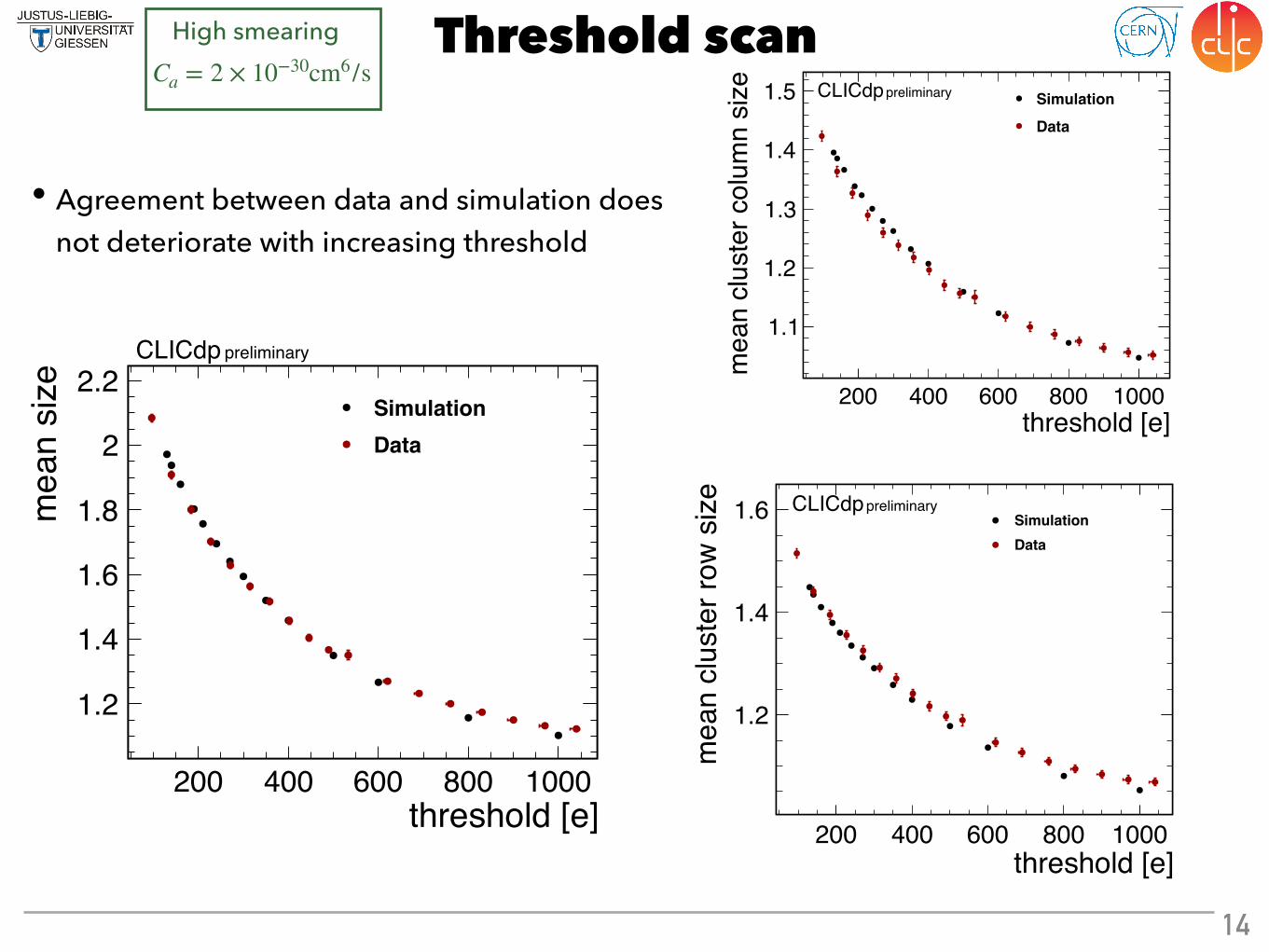
Threshold scan
200 400 600 800 1000threshold [e]
1.2
1.4
1.6
1.8
2
2.2
mea
n si
ze SimulationData
CLICdp preliminary
200 400 600 800 1000threshold [e]
1.1
1.2
1.3
1.4
1.5
mea
n cl
uste
r col
umn
size Simulation
Data
CLICdp preliminary
200 400 600 800 1000threshold [e]
1.2
1.4
1.6
mea
n cl
uste
r row
siz
e
SimulationData
CLICdp preliminary
High smearing
• Agreement between data and simulation does not deteriorate with increasing threshold
14
Ca = 2 × 10⁻³⁰cm6/s

Rotation scan
20 30 40 50 60 70rotation angle
1
1.5
2
2.5
3
3.5
4
mea
n cl
uste
r col
umn
size CLICdp preliminary
• Sensor is tilted in column direction
• Charge carriers created in or close to the substrate are expected to have a stronger contribution to the cluster size for increasing rotation angles
Column direction
Not to scale
Subs
trate
Data - 300 um thick sampleData - 50 um thick sample
Simulation
15
High smearing
Thrd = 170eCa = 2 × 10⁻³⁰cm6/s
16
SUMMARY AND OUTLOOK
• Comparison of simulation against FastPix measurements (analogue information available)
A thousand thanks to Magdalena and Simon for their invaluable support and supervision for this work
• Charge carrier recombination models (Shockley-Read-Hall and Auger recombination) have been implemented
• Effective charge carrier lifetime is determined by these models and not by integration time
• Ignorance of exact doping profiles introduces uncertainties in the simulation
Outlook
Summary
• Studying impact of additional variations in the doping profiles on the cluster observables
Thank you for your attention
• TCAD+APSQ simulations for 65 nm process

Back-up

18
CHARGE CARRIER RECOMBINATION
Tucher, Nico. (2016). Analysis of photonic structures for silicon solar cells.

In-pixel cluster size differenceHigh smearing
0 10 20 30x [um]
0
5
10
15
20
25
30
y [u
m]
1.5−
1−
0.5−
0
0.5
diff
siz
e
0 10 20 30x [um]
0
5
10
15
20
25
30
y [u
m]
0.6−0.5−0.4−0.3−0.2−0.1−
00.10.20.3
diff
x s
ize
0 10 20 30x [um]
0
5
10
15
20
25
30
y [u
m]
0.8−
0.6−
0.4−
0.2−
00.20.4
diff
y s
ize
Ca = 2 × 10⁻³⁰
Thrd = 170e