3D heterostructures and systems for novel MEMS/NEMS - IOPscience
10
Science and Technology of Advanced Materials TOPICAL REVIEW 3D heterostructures and systems for novel MEMS/NEMS To cite this article: Victor Yakovlevich Prinz et al 2009 Sci. Technol. Adv. Mater. 10 034502 View the article online for updates and enhancements. You may also like VHF NEMS-CMOS piezoresistive resonators for advanced sensing applications Julien Arcamone, Cécilia Dupré, Grégory Arndt et al. - Scalable fabrication of carbon-based MEMS/NEMS and their applications: a review Shulan Jiang, Tielin Shi, Xiaobin Zhan et al. - CMOS and NEMS Hybrid Architectures Thomas Ernst, Issam Ouerghi, Willy Ludurczak et al. - Recent citations 3D printing methods for micro- and nanostructures K B Fritzler and V Ya Prinz - CAD/CAM for scalable nanomanufacturing: A network-based system for hybrid 3D printing Hae-Sung Yoon et al - Editorial Nuggehalli M. Ravindra - This content was downloaded from IP address 194.39.196.6 on 03/12/2021 at 01:40
Transcript of 3D heterostructures and systems for novel MEMS/NEMS - IOPscience

Science and Technology ofAdvanced Materials
TOPICAL REVIEW
3D heterostructures and systems for novelMEMS/NEMSTo cite this article: Victor Yakovlevich Prinz et al 2009 Sci. Technol. Adv. Mater. 10 034502
View the article online for updates and enhancements.
You may also likeVHF NEMS-CMOS piezoresistiveresonators for advanced sensingapplicationsJulien Arcamone, Cécilia Dupré, GrégoryArndt et al.
-
Scalable fabrication of carbon-basedMEMS/NEMS and their applications: areviewShulan Jiang, Tielin Shi, Xiaobin Zhan etal.
-
CMOS and NEMS Hybrid ArchitecturesThomas Ernst, Issam Ouerghi, WillyLudurczak et al.
-
Recent citations3D printing methods for micro- andnanostructuresK B Fritzler and V Ya Prinz
-
CAD/CAM for scalablenanomanufacturing: A network-basedsystem for hybrid 3D printingHae-Sung Yoon et al
-
EditorialNuggehalli M. Ravindra
-
This content was downloaded from IP address 194.39.196.6 on 03/12/2021 at 01:40

IOP PUBLISHING SCIENCE AND TECHNOLOGY OF ADVANCED MATERIALS
Sci. Technol. Adv. Mater. 10 (2009) 034502 (9pp) doi:10.1088/1468-6996/10/3/034502
TOPICAL REVIEW
3D heterostructures and systems fornovel MEMS/NEMSVictor Yakovlevich Prinz, Vladimir Alexandrovich Seleznev,Alexander Victorovich Prinz and Alexander Vladimirovich Kopylov
Institute of Semiconductor Physics, Russian Academy of Sciences, Siberian Branch,Lavrent’ev Avenue 13, Novosibirsk 630090, Russia
E-mail: [email protected]
Received 21 January 2009Accepted for publication 24 May 2009Published 14 July 2009Online at stacks.iop.org/STAM/10/034502
AbstractIn this review, we consider the application of solid micro- and nanostructures of variousshapes as building blocks for micro-electro-mechanical or nano-electro-mechanical systems(MEMS/NEMS). We provide examples of practical applications of structures created byMEMS/NEMS fabrication. Novel devices are briefly described, such as a high-powerelectrostatic nanoactuator, a fast-response tubular anemometer for measuring gas and liquidflows, a nanoprinter, a nanosyringe and optical MEMS/NEMS. The prospects are describedfor achieving NEMS with tunable quantum properties.
Keywords: micro-electro-mechanical systems (MEMS), nano-electro-mechanical systems(NEMS), MEMS/NEMS heterostructures
(Some figures in this article are in colour only in the electronic version)
1. Introduction
Micro-electro-mechanical systems (MEMS) are awell-established R&D field. Fabrication methods forMEMS building blocks and various applications of MEMShave been described in detail in numerous publications(see [1–4], for instance). In terms of fabrication, MEMS arecurrently dominated by planar processing techniques, whichare based on silicon integrated circuit (IC) technology.The planar approach and the strong dependence onsilicon worked well in the early years because manyprocessing tools and methodologies that are commonlyused in IC fabrication could be directly applied for thefabrication of MEMS devices. The considerable progress inMEMS was due to the full exploitation of the mechanicaldegree of freedom and the evolution to 3D structures.Here, bulk micromachining, surface micromachining andLIGA (from German: Lithographie, Galvanoformung,Abformung) technologies have contributed substantially tothe already existing possibilities [5]. Structures fabricatedby these processes include comb electrostatic actuators.
Other well-known applications of such processes includeMEMS cavities in inkjet printers and MEMS sensors inautomobiles [2].
Presently, we are witnessing a transition from MEMSto nano-electro-mechanical systems (NEMS) that offer newexciting applications [3, 4]. In the transition from MEMS toNEMS, the feature sizes are reduced, making the fabricationmethods previously developed for MEMS unsuitable forthe production of high-precision NEMS elements. On theother hand, nanomechanical devices require precise 3Dnanostructures whose parts move at nanometer scale. Thekey challenge in NEMS is therefore the development of newmethods for routine reproducible nanofabrication.
Several approaches to solving this problem arepresently available. For instance, 3D nanostructureshave been fabricated using a focused electron beam [6].Electron-beam-induced deposition is a promising techniquefor maskless nanofabrication that has been studied by manyresearchers because of its higher resolution due to the smallerbeam spot, and because of the possibility of combining
1468-6996/09/034502+09$30.00 1 © 2009 National Institute for Materials Science Printed in the UK

Sci. Technol. Adv. Mater. 10 (2009) 034502 Topical Review
(d) (e)
Figure 1. Schematic illustration of the strain-driven fabrication of shells. The interatomic elastic forces in the lower layer (F1) and theupper layer (F2) are oppositely directed, giving rise to a nonzero moment of forces M . Under the action of this moment, the initially planarbilayer bends or rolls up into the shape of a scroll [7]. Scanning electron microscopy (SEM; a, d, e) and high-resolution transmissionelectron microscopy (HRTEM; b, c ) images of rolled-up InGaAs/GaAs nanotubes formed from bilayered films [7]. (d) and (e)InGaAs/GaAs 3D open shells obtained by lithography and directional rolling [9].
top-down and bottom-up approaches. There is no doubtthat this technique, enabling the fabrication of many 3Dstructures, will be widely used. This method can also beused as a supplementary tool. It should be noted, however,that this approach uses a successive process; as a result,the time necessary for batch nanofabrication may becomeunacceptably long.
It is therefore acutely recognized that a parallel processfor fabricating 3D nanostructures is required, ensuringnanoscale sizes and near-atomic precision in fabricatedNEMS. In addition, efficient nanotechnology should beapplicable to various materials and allow the formation ofvariously shaped, scalable structures necessary for practicalapplications. Such technology should also be robust andcompatible with the well-established procedures for theepitaxial growth of nanostructures, as well as with planarprocessing techniques, and should use already existing plantsand facilities. To meet these requirements, a technologyhas been introduced [7–9] that enables the formation ofprecise 3D shell nanostructures of various shapes. Thistechnology has been used to fabricate tubes with diametersdown to 2 nm, helices with diameters down to 7 nm, andperiodically corrugated structures with corrugation periodsdown to 10 nm. It has been demonstrated to be suitable for thebatch production of precise 3D structures for use in NEMS.
The new technology is based on the use of high-precisioninitial plane structures and systems, and also on the use ofself-forming and self-assembling processes for the fabricationof precise 3D objects capable of executing mechanicalmotion, elastically changing their shape and so forth [7, 8].In [8], a new concept of fabricating building blocks fornanoelectronic and nanomechanic devices was discussed. Inthe present paper, we summarize the results obtained in the
pilot development of MEMS and NEMS, and show how theproposed concept can be used in the formation of buildingblocks for micro- and nanomechanical devices. The examplesof building blocks and experimental structures given in thispaper merely illustrate the simplest 3D structures. The nextdevelopmental stage in this field will be the adaptation of thistechnology to the fabrication of multilayered 3D structuresand materials.
2. Fabrication principles and classificationof structures
For high-performance MEMS/NEMS, 3D structures arerequired to exhibit the free motion of their parts. Suchstructures must be fabricated with high precision. However,until recently no standard processes were available forfabricating 3D building blocks with atomic or nanometeraccuracy. In recent years, there has been a clear tendencytowards the use of 3D rather than planar building blocks [5].Another tendency, towards using new materials in MEMS,was discussed in detail in [10, 11]. The previously usedapproaches were primarily based on LIGA technology whichhas contributed greatly to the formation of 3D MEMSmicrostructures. LIGA processes, however, are restricted tomicrometer sizes, whereas the precision of NEMS fabricationmust be of nanometer or atomic scale [2].
The general approach to the formation of semiconductornanotubes and other 3D nanoshells [7–9] is illustrated infigures 1 and 2. The initial structure includes a sacrificiallayer and a bilayered heterofilm that is strained as a resultof the lattice mismatch with the substrate. After selectiveremoval of the sacrificial layer, the strained heterofilm bends,
2
Sci. Technol. Adv. Mater. 10 (2009) 034502 Topical Review
(a) (b) (c)
Figure 2. (a) Schematic illustration of buckling of compressed layer after its partial detachment from the substrate resulting from selectiveetching of the underlying AlAs sacrificial layer. (b) SEM cross-sectional images of buckled and corrugated InGaAs–GaAs structures [8].(c) 3D image of SiGe/Si corrugated film obtained using atomic force microscopy [12].
rolls, or buckles because of internal elastic forces, formingthe final elastic shell structure. The curvature radius of thefinal 3D shell is precisely defined by the mechanical strainand by the thicknesses of the constituent layers in the initialplanar structure. In the simple case of an initial planar bilayerstructure we have
R =2
3d
a
1a, (1)
where d is the thickness of each layer and 1a/a is the latticemismatch between the layers. The thicknesses of the layers, aswell as the mechanical strain induced by the lattice mismatchbetween the layers, can be controlled with extreme precision,thus enabling precise control of the curvature radius fromone nanometer to hundreds of micrometers (for a review,see [8, 9]). A great variety of shell designs have now beendemonstrated, and many other configurations can be formedon one substrate. Semiconductors, metals, or dielectrics canbe used as materials for this technology.
Figure 1 illustrates closed shells (a–c) and open shells(d, e) fabricated in the described manner. Open shells are verysensitive to mechanical forces, whereas closed shells werefound to be extremely rigid. Our experiments showed thatInGaAs/GaAs tubes (closed shells) of 1 µm diameter, 10 nmwall thickness and 100 µm length can be elastically loadedwith a force of 0.1 N [7].
The formation of nanobuckles and the possibilityof controlling their dimensional parameters were firstdemonstrated in [8]. The fabricated nanocorrugated systemshad periods of up to 10 nm [8, 9]. Figure 2 illustratesa nanocorrugated (nanobuckled) film prepared from acompressed, initially flat film locally detached from asubstrate. Such corrugations can be formed because locallyreleased compressed planar films are unstable and tend tobuckle. The buckled shape results from the simple elongationof the released films in the direction along the edge [12].This technology is being further developed by many researchgroups [13–15].
The fabrication technology includes the followingcritical points: (i) the highly selective etching of sacrificiallayers [7]; (ii) the directional rolling up of films, yielding3D micro- and nanoshells of various shapes [16–18];(iii) the assembly of micro- and nanoshells into morecomplex architectures [19]; (iv) the super-critical drying ofnanoshells [20]; and (v) the formation of nanoshells whosesizes can be precisely controlled in three dimensions [21].
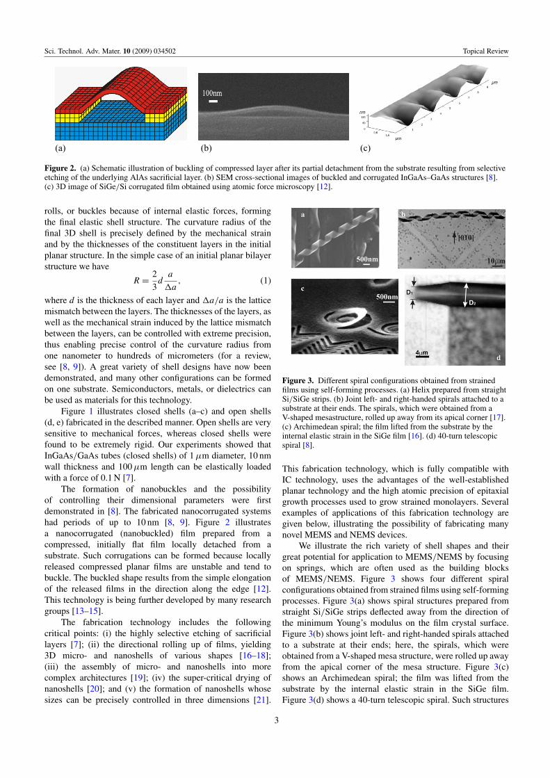
Figure 3. Different spiral configurations obtained from strainedfilms using self-forming processes. (a) Helix prepared from straightSi/SiGe strips. (b) Joint left- and right-handed spirals attached to asubstrate at their ends. The spirals, which were obtained from aV-shaped mesastructure, rolled up away from its apical corner [17].(c) Archimedean spiral; the film lifted from the substrate by theinternal elastic strain in the SiGe film [16]. (d) 40-turn telescopicspiral [8].
This fabrication technology, which is fully compatible withIC technology, uses the advantages of the well-establishedplanar technology and the high atomic precision of epitaxialgrowth processes used to grow strained monolayers. Severalexamples of applications of this fabrication technology aregiven below, illustrating the possibility of fabricating manynovel MEMS and NEMS devices.
We illustrate the rich variety of shell shapes and theirgreat potential for application to MEMS/NEMS by focusingon springs, which are often used as the building blocksof MEMS/NEMS. Figure 3 shows four different spiralconfigurations obtained from strained films using self-formingprocesses. Figure 3(a) shows spiral structures prepared fromstraight Si/SiGe strips deflected away from the direction ofthe minimum Young’s modulus on the film crystal surface.Figure 3(b) shows joint left- and right-handed spirals attachedto a substrate at their ends; here, the spirals, which wereobtained from a V-shaped mesa structure, were rolled up awayfrom the apical corner of the mesa structure. Figure 3(c)shows an Archimedean spiral; the film was lifted from thesubstrate by the internal elastic strain in the SiGe film.Figure 3(d) shows a 40-turn telescopic spiral. Such structures
3

Sci. Technol. Adv. Mater. 10 (2009) 034502 Topical Review
can also be obtained from a film with thickness gradientalong the strip, which results in a gradient of curvature radiusalong the surface. Figures 1(d) and 1(e) show a system ofspirals also prepared from a system of strips. It is possibleto fabricate a variable-pitch, variable-diameter spiral from abilayer film with variable thickness of the top layer; in thiscase, the elastic force bending the film also varies along thesurface. These simplest 3D shells can be used in actuators,such as those described in [22], and sensors, including thesupersensitive sensors described in [23]. It should be notedthat such shells can be formed from many materials, includingsemiconductors, dielectrics and metals. Of prime importancehere are shells formed from hybrid films and shells in whichsemiconductor layers are used as shape-generating elements.
In addition, this technology is ideal for the formation ofNEMS owing to the following features. Firstly, it is scalabledown to nanometer dimensions, enabling the formationof shells with molecular- and atomic-level thicknesses.Secondly, this technology allows shell fabrication withhigh precision. Thirdly, it is perfectly compatible with thewell-established planar lithographic technology used forICs. Fourthly, it allows to produce a rich variety of shellshapes made of various materials. This technology, initiallydeveloped for the formation of semiconductor micro- andnanoshells, has subsequently been extended to the formationof hybrid metal-semiconductor shells [24], metal micro-and nanoshells [25], organic nanoshells [26] and metalshells formed from strained layers deposited onto polymerfilms [27]; these processes offer additional possibilities innanofabrication.
The developed technology meets all the requirementsfor NEMS fabrication and offer high performance for thefabrication of freestanding, multilayered and self-assemblingstructures.
3. Novel micro- and nanoactuators
Nowadays, the fabrication of solid-state nanoactuators isstill a challenging problem, and active research to find newapproaches towards solving this problem is under way.
The rich variety of shapes offered by elastic shellsformed from strained films of many materials opensup wide possibilities for the creation of various micro-and nanoactuators and sensors. A simple artificialactuator developed around spiral shells is given as anexample [22]. The proposed structure allows the developmentof self-propelled devices and swimming microrobots, whichmimic bacterial flagella in both size and motion. The swimmerconsists of an InGaAs/GaAs or InGaAs/GaAs/Cr helicaltail and a thin soft-magnetic head. These magnetically drivenhelical devices can be used as wireless manipulators formedical and biological applications under three-dimensionalcontrol in fluid environments [23, 28]. In [27], a catalytictubular microjet is described, which was rolled up from aTi/Fe/Au/Ag multilayer nanomembrane. Inside the microjet,hydrogen peroxide (H2O2) is decomposed into O2 bubblesand water by a catalytic reaction of H2O2 with the inner Agnanotube wall.
Figure 4. Schematic of a simple electrostatic capacitor actuator.
The simplest and most widespread actuators use theelectrostatic attraction force acting between two parallelplates (usually, one plate is fixed and the other is moving).Electrostatic micro- and nanoactuators are easy to designand fabricate, and they are easily integrated in micro-and nanosystems. They are applied in radio engineeringas active filters or resonators, and also in hydrodynamicsystems. They can be employed as pumps for liquids orfinely dispersed materials, as atomizers for liquid droplets,and also as accelerometers and sensors in many industries.These electrostatic nanoactuators are very promising owingto the high energy density accumulated in these devices andthe large force that they can generate. These factors areparticularly advantageous in scaling the separation betweenthe plates down to nanometer dimensions. The high accuracydesired in the formation of such super narrow nanogaps canbe achieved by molecular-beam epitaxy, which can yieldstructures with perfectly controlled separation between thelayers. A disadvantage of such actuators is their insufficientstability: they suffer from pull-in phenomena [29, 30].Moreover, the range of stable displacements in such actuatorsis much smaller than the initial separation between theelectrodes.
Let us consider an electrostatic actuator formed by twoparallel plates of area A with separation g0 between theplates (figure 4). Neglecting edge phenomena, the energyaccumulated in such an actuator–capacitor is defined bythe voltage V applied to the plate electrodes and by thecapacitance C of the capacitor:
W =1
2CV 2
=ε0 AV 2
2g0. (2)
The force acting between the plates is
F =dW
dg=
ε0 AV 2
2g20
. (3)
Thus, the force F is a nonlinear function of the potentialand of the separation between the plates. For such a system toact as an actuator, one or both plates should be movable andfixed to an elastic compensator. A spring [31–34] or a viscousliquid [35] can be used as the compensator. The system is
4

Sci. Technol. Adv. Mater. 10 (2009) 034502 Topical Review
at equilibrium when the elastic force due to the spring isbalanced by the electrostatic attracting force:
kx =ε0 AV 2
2(g0 − x)2. (4)
Here, kx is the elastic force generated by the spring, andthe right-hand side is the electrostatic attraction force. Theelastic force varies linearly with x , whereas the electrostaticforce is nonlinear with respect to x . An equilibrium state ofthe system is only possible if the electrostatic force is lessthan or equal to the elastic force. At some voltage Vpull-in
the electrostatic force becomes greater than the elastic force,the system becomes unstable and the capacitor plates comein contact. Normally, such a state emerges at x ≈ 0.3g0; thismeans that the controlled electrostatic force developed inthe actuator is almost 50 times smaller than the force thatwould be developed in the case of x ≈ 0.9g0 (see the formulaabove). The pull-in effect is the main shortcoming of capacitorsystems because it strongly limits the range of displacementsand the force generated in the actuator. Various liquids canbe used to avoid this effect [35]. However, this results in thecatastrophic deterioration of all performance characteristics ofthe actuator.
In [36, 37], we proposed an alternative electrostaticactuator without this shortcoming. In the new actuator, anelastic corrugated film, acting as a variable-rigidity spring,is installed between the two parallel plates. As the biasvoltage applied to the electrodes increases, the corrugated filmdeforms and switches between states with a consecutivelyincreasing number of corrugation periods and decreasingcorrugation amplitude (see figure 5). This allows us to obtainnanogaps between electrodes and to dramatically increasethe electrostatic attraction. It should be noted that as theelectrodes approach each other, both the attractive forceand the actuator power increase (the electrostatic force isinversely proportional to the square of the separation betweenthe plates). A specific feature of corrugated nanofilms istheir ability to withstand enormous mechanical stresses [12].Upon removing the voltage, the actuator, after passingthrough intermediate successive states, reacquires its initialconfiguration. Numerical calculations and experimental testshave shown that such variable-rigidity actuators, whichhave a considerable range of displacements, are capable ofgenerating forces of up of to 105 N cm−2 [36, 37].
Such actuators were experimentally realized witha GaAs/AlAs/InGaAs/AlAs/GaAs structure and ahybrid structure (substrate/corrugated film/ferroelectricfilm/semiconductor film). Special monolayer coatings wereused to prevent sticking. For Si/SiGe/Si structures, we used1-octadecene monolayers [38]. The tests were performedusing capacitance methods for measuring the separationbetween the electrodes. The small dimensions of the actuatorand the possibility of low control voltages (< 5 V at a 100 nminitial gap and 6 nm thickness of the corrugated film) makethe device promising for nanoscale applications.
(a)
(b)
Figure 5. (a) Schematic illustration of the operating sequence of avariable-rigidity actuator. An increase in the bias voltage leads to anincreased load acting on the corrugated film, causing the film tosequentially switch into states with a greater number of periods andsmaller corrugation amplitude (from top to bottom). The upwardarrows show the reverse process upon decreasing the bias voltage.(b) Cross-sectional view of an experimental actuator structurefabricated from an initial GaAs/AlAs/InGaAs/AlAs/GaAsstructure by etching the AlAs sacrificial layer [36, 37].
4. Hot-tube sensors as basic elements for smartcontrol of turbulence systems
The nanometer thicknesses of micro- and nanoshells, thehigh stability and precision of their shapes, and their goodreproducibility in batch production open up wide possibilitiesin the application of such shells in intelligent micro- andnanosystems, and also in sensors and actuators. Otherapplications of 3D elastic nanostructures include sensors,actuators for MEMS/NEMS and smart systems based onsuch structures. The replacement of bulk sensor/actuatorcomponents with nanoshells drastically improves thesensitivity and response rate of the devices. Below, wegive one example in which the replacement of a wire withan ultrathin-walled tube (1–100 nm) reduces the thermalinertia of a sensor or actuator by two orders of magnitude.This improves the response speed of sensors and actuators,allows the detection and suppression of rapidly develop-ing turbulence, and assists the development of smart
5

Sci. Technol. Adv. Mater. 10 (2009) 034502 Topical Review
Figure 6. Amplitude–frequency characteristics of hot-wire (a) andhot-tube (b) sensitive elements. For the hot-tube probe, the timeconstant is 100 times smaller than that for the standard hot-wireprobe, which enables us to considerably extend the frequency rangeof measurements and to study rapid processes that generateturbulence at high flow velocities [44, 45].
control systems providing a laminar flow regime around newaircraft.
The control of the laminar–turbulent transition in theboundary layer is a long-standing practical challenge inthe field of gas dynamics and hydrodynamics. If solved,it will enable a significant reduction of drag for movingaircraft and the enhanced efficiency of air transport.The potential benefits of flow control include improvedperformance and maneuverability, affordability, increasedrange and payload, drag reduction, lift enhancement, mixingaugmentation, heat-transfer enhancement and the suppressionof flow-induced noise [39].
Recently, a prototype feedback control system for wallturbulence has been developed [40]. Arrays of micro hot-filmsensors were employed to measure streamwise shear stressfluctuations, while arrays of magnetic actuators were used tointroduce control input through wall deformation. A digitalsignal processor was employed to drive the actuators based onsensor signals. Feedback control experiments were performedin a turbulent air channel flow, and it was found that thewall shear stress (drag) could be decreased by up to 7%. Amajor deficiency of presently developed systems is a very longresponse time (∼ms), which restricts the application of suchsystems to low-velocity subsonic flow conditions [40, 41].
Heated wires, cooled by flowing gas, are widely used asflow sensors (hot-wire anemometry) [42]. In [43], it wasshown that the replacement of hot wires with hot microtubes(see figure 6) improves the response time by a factor of 100.This property of tubular hot-wire sensors allows their use insupersonic flow systems operating at frequencies above1 MHz.
In [44, 45], it was also shown that microtubes heated in apulsed mode can be used as sensors and actuators; moreover,one and the same tube can be used as both a sensor and anactuator in smart turbulence control systems.
The tubular components are connected to control andreadout devices using conductor lines located on the substrate
(figure 7). The figure shows electron microscopy images ofa chip with an array of hybrid microtubes rolled up from aSiO2/Si3N4/Au heterofilm. The total thickness of the wallsin the SiO2/Si3N4/Au microtubes was 90 nm, and the tubediameter was about 10 µm.
The above example is suitable for gas-dynamicsapplications, with the tube wall thickness in the nanometerrange and the tube diameter preset in the micrometer range.Because the shell technology can be scaled down to thenanometer region, the use of nanoscale hot-tube sensors andsmart control systems based on such sensors is realistic in bothhydrodynamic and nanofluidic applications.
5. Elements for micro- and nanofluidicMEMS/NEMS
Microfluidics and its applications to a lab-on-a-chip aredescribed in [2]. The fundamentals of nanofluidics and thephysics of liquid jets have been considered thoroughly in [46].
To deliver DNA and other biologically importantmolecules into a living cell, a micro-needle (or pipette)penetrating the membrane is used for microinjection [47].However, the large pipette size and injection volume candamage cells. Smaller needle diameters (submicro- andnanometer) would enable new applications for these objectssuch as the handling and dissection of individual biologicalcells and chromosomes, and accurate microinjection intoliving cells.
The use of semiconductor technology in this fieldallows the mass production of such instruments. Manygroups have conducted extensive research into the fabricationand application of micromachined microneedles [48–53].Rolled-up tubes are also highly promising elements for therealization of nanofluidic MEMS/NEMS suitable for batchproduction. Indeed, rolled-up nanotubes with a broad rangeof lengths and diameters can be formed from semiconductorsby a process perfectly compatible with planar and ICtechnologies.
Because of their very thin walls, rolled-up tubes offermuch promise for use in microinjection systems. Rolled-upsemiconductor microtubes were experimentally shown topossess a mechanical strength sufficient for the multiplepiercing of plant cell walls [48, 49].
Below, an example is given in which structuring wasachieved by the successive action of elastic forces. Figure 8illustrates the formation of needles extending beyond the edgeof a chip substrate. It can be clearly seen that the tubesare rolled at the first stage (a). At the second stage (b), theformed tubes become oriented upward under the action ofinternal elastic forces, thus forming a structure with a needleprotruding over the substrate edge. Figure 8 shows examplesof needles with atomically sharp edges, which were used forthe development of micro- and nanosyringes and micro- andnanoneuroprobes [49].
An atomic-force microscope offers unrivaled running andpositioning accuracy, which cannot be obtained using manualmicroactuators. The use of an atomic-force microscope fortransfection was demonstrated for the first time in [54, 55]
6

Sci. Technol. Adv. Mater. 10 (2009) 034502 Topical Review
Figure 7. System of electrically conducting thin-walled microtubes with electrical contacts: (a) schematic of a chip with an array ofmicrotubes; (b) SEM image of chip with microtubes fabricated from a SiO2/Si3N4/Au heterofilm (the tubes are suspended above the pitsetched in the Si substrate); (c) enlarged image of one of the microtubes in (b) [44, 45].
(a) (b) (c)
Hinge
Tube
Figure 8. Formation of a tube protruding over the substrate edge. Scheme (a, b) and resultant Si/SiGe structure (c) [49].
Figure 9. (a) Schematic view of a nanocorrugated structure. (b) Cross-section of the bilayer structure shown in (a): in the top layer, regionslabeled 1 are under tensile stress, and regions labeled 2 are under compressive strain. (c) Confinement potential for electrons near the uppersurface of the film (solid line) and the lower electron level (dashed line) [69].
using modified cantilevers with pointed tips. The microscopeallows one to adjust the force applied to a cell and is thereforea very sensitive precision instrument. Several authors haveused cantilevers modified with carbon nanotubes to puncturecell walls [57] and introduce molecules into living cellswith the help of cantilever-mounted carbon nanotubes. Thenanotubes were modified with a disulfide linker to fix aquantum dot covered with a protein [58]. It should be noted,however, that modified cantilevers and carbon nanotubes fixedat the needle point are rather costly to fabricate. In addition,
such cantilevers cannot be used to dissect cells because theyhave no cutting edges.
Recently, we have fabricated cantilevers with tips,prepared as rolled-up tubes. Our initial experiments showedthat rolled-up semiconductor nanotubes offer substantialadvantages for cell puncture in comparison with carbontubes.
Such tubes can be used for the development of nanojetprinters [59]. In our experiment, a solution contained in
7

Sci. Technol. Adv. Mater. 10 (2009) 034502 Topical Review
a microtube was locally heated by a resistive microheaterprepared from Ni foil. Upon applying electric current pulses,the ink in the tube boiled locally, causing bubbles to formand liquid droplets to jet out of the tube. Minimum dropdiameter of 100 nm was achieved using an inkjet preparedfrom a 200-nm diameter tube.
These examples demonstrate the potential capabilities ofthe technology in micro- and nanofluidic applications. Thesecapabilities are based on the possibility of forming, usingthe new process, various nanoshells with perfectly controlledsizes that can be scaled down to nanometer region.
6. Building blocks for optical MEMS/NEMS
Extreme precision, a large variety of designs, wide-rangescaling, the possibility of 3D arrangements and a parallelfabrication process make 3D shells ideal elements for variousnovel materials, particularly, for metamaterials, which presentnew opportunities for controlling electromagnetic radiation(for example, see reviews [60, 61]). 3D shells were used tocreate chiral structures and metamaterials in [62, 63]. Suchshells can be used to create metamaterials with a negativeindex of refraction, and also magnetic and bianisotropicmetamaterials that can control radiation over a widespectral range, from microwaves to visible light. Arrays ofprecise hybrid metal-semiconductor helical microresonatorswere recently fabricated from strained bilayer films [63](figures 1(d) and (e)). A maximum angle of polarizationplane rotation in the microwave range (135–145 GHz) of90◦ was achieved using an array of parallel helices orientedparallel to the wave direction, with a pitch close to thewavelength of microwave radiation. Giant rotation of thepolarization plane of radiation by arrays of helices in the THzrange was examined in [62, 63]. The elasticity andextreme shape stability of out-of-plane freely suspendedshell resonators allow control of the shell shapes andthe electromagnetic properties of shell-based metamaterials,respectively. The full compatibility of the method used withIC technology facilitates high-speed dynamic polarizationcontrol. The integration of shell helices with NEMS for theelectromechanical control of helix geometry is very promisingfor the formation of solid-state metamaterials analogous toliquid crystals that can control radiation in different spectralranges. Above, we considered 3D structures formed by thinfilms of nanometer thickness. Our recent experiments showedthat the structuring method enabling the formation of 3Dnanostructures can be successfully transferred to films ofatomic thickness [64].
7. Prospects for NEMS with tunablequantum properties
Conducting nanoshells exhibit unusual quantum properties(see, for instance [65–69]), which can be further controlledby displacing parts of such elastic systems at the nanoscale.
There are a few strategies for providing mechanicalsystems with tunable quantum properties. The shuttleproposed in [65] is one of the most well-known mechanical
systems employing quantum properties. Using such a shuttle,for instance, single-electron transfer can be achieved. Weexpect that shuttling devices for electrons can be fabricatedusing the above-discussed technology for 3D shells. Also,even simpler ways are presently available for the fabricationof NEMS with tunable quantum properties.
The conformal transformations of shells analogous to theconformal transformations of molecules that widely occur innature are of much interest to us. Upon the modification of themolecular configurations, the molecular properties may alsoexhibit considerable changes [70].
Below, we describe the possibility of mechanicallycontrolling shell shapes and, hence, the quantum propertiesof modified structures. In section 3 and in [12] we showedthat under the action of electrostatic forces the corrugationconfiguration can undergo dramatic modifications, leading,for instance, to a sequential decrease in the corrugation periodand film-bending radius.
When a film bends, its outer layers stretch and its innerlayers compress, and the strain εs in the direction alongthe surface varies linearly across the film [71, 72]: εs =
h/R, where h is the thickness of the film and R is itscurvature radius calculated by differential geometry formulae.Calculations of a nanocorrugated structure [69] revealed thatthe film bends can produce deep quantum wells (up to1 eV deep for thin InAs films). When an external action isexerted on such a corrugated film (see section 3), a systemcan be obtained with tunable quantum properties at roomtemperature.
The transformation of corrugated structures by applyingan external force was demonstrated in [12, 36, 37].Undoubtedly, complex shells that are reconfigurable byelectrostatic forces will form a basis for novel NEMS.
8. Conclusion
We have described some novel applications of precise3D shell structures (powerful electrostatic nanoactuators,ultrafast tubular anemometers for measuring gas flows,elements for micro- and nanofluidic MEMS/NEMS, opticalMEMS/NEMS). We have presented examples of preciselyfabricated MEMS/NEMS devices based on semiconductors,metals, and hybrid micro- and nanoshells. Novel sensors andactuators and smart materials are briefly described. Finally, weoutlined prospects for achieving NEMS with tunable quantumproperties.
Acknowledgments
This work was supported by the Russian Foundation for BasicResearch and by the Russian Government (Federal Programs).
References
[1] Cleland A 2003 Foundations of Nanomechanics(Berlin: Springer)
[2] Bhushan B 2004 Springer Handbook of Nanotechnology(Berlin: Springer)
8

Sci. Technol. Adv. Mater. 10 (2009) 034502 Topical Review
[3] Goddard W A III, Brenner D W, Lyshevski S E and Iafrate G J2002 Handbook of Nanoscience, Engineering, andTechnology (Boca Raton, FL: CRC Press)
[4] Li M, Tang H X and Roukes M L 2007 Nat. Nanotechnol.2 114
[5] Becker E W, Ehrfeld W, Hagmann P, Maner A andMunchmeuer B 1986 Microelectron. Eng. 4 35
[6] Furuya K 2008 Sci. Technol. Adv. Mater. 9 014110[7] Prinz V Ya, Seleznev V A, Gutakovsky A K, Chehovskiy A V,
Preobrazenskii V V, Putyato M A and Gavrilova T A 2000Physica E 6 828
[8] Prinz V Ya 2003 Microelectron. Eng. 69 466[9] Prinz V Ya 2006 Phys. Status Solidi b 243 3333
[10] Wilson S et al 2007 Mater. Sci. Eng. R 56 1[11] Liu C 2007 Adv. Mater. 19 3783[12] Prinz A V and Prinz V Ya 2008 Proc. 16th Int. Symp. on
Nanostructures: Physics and Technology pp 147–8Prinz A V and Prinz V Ya 2006 Russian Patent No. 2278815
[13] Cho A 2006 Science 313 164[14] Scott S A and Lagally M G 2007 J. Phys. D: Appl. Phys.
40 R75[15] Li X 2008 J. Phys. D: Appl. Phys. 41 193001[16] Prinz V Ya, Grutzmacher D, Beyer A, David C, Ketterer B
and Deccard E 2001 Nanotechnology 12 399[17] Prinz A V and Vorob’ev A B 2002 Semicond. Sci. Technol.
17 614[18] Golod S V, Prinz V Ya and Mashanov V I 2005 Thin Solid
Films 489 169[19] Prinz V Ya, Vorob’ev A B and Seleznev V A 2001
Inst. Phys. Conf. Ser. 170 319[20] Seleznev V A, Yamaguchi H, Hirayama Y and Prinz V Ya
2003 Japan. J. Appl. Phys. 42 L79[21] Prinz V Ya, Chekhovskiy A V, Preobrazhenskii V V, Semyagin
B R and Gutakovsky A K 2002 Nanotechnology 13 231[22] Zhang L, Abbott J J, Dong L, Kratochvil B E, Bell D and
Nelson B J 2009 Appl. Phys. Lett. 94 064107[23] Grutzmacher D, Zhang L, Dong L, Bell D, Nelson B,
Prinz A V and Ruhd E 2008 Microelectron. J. 39 478[24] Prinz V Ya and Golod S V 2006 J. Appl. Mech. Tech. Phys.
47 867[25] Nastaushev Yu V, Prinz V Ya and Svitasheva S N 2005
Nanotechnology 16 908[26] Luchnikov V, Sydorenko O and Stamm M 2005 Adv. Mater.
17 1177[27] Mei Y, Huang G, Solovev A, Bermudes E, Monch I, Ding A,
Reindl T, Fu R, Chu P and Schmidt O G 2008 Adv. Mater.20 4085
[28] Bell D J, Dong L, Nelson B J, Golling M, Zhang L andGrützmacher D 2006 Nano Lett. 6 725
[29] Nemirovsky Y and Degani O 2001 J. Micromech. Syst. 10 601[30] Degani O, Socher E, Lipson A, Leitner T, Setter D J, Kaldor S
and Nemirovsky Y 1998 J. Micromech. Syst. 7 373[31] Bermejo S et al 2008 J. Micromech. Microeng. 18 055004[32] Seeger J I and Boser B E 2003 J. Microelectromech. Syst. 12
656[33] Li Y, Packirisamy M and Bhat R 2008 Microsyst. Technol. 14
255–66[34] Guo J G and Zhao Y P 2006 Int. J. Solids Struct. 43 675[35] Rollier A S et al 2006 J. Micromech. Microeng. 16 794[36] Prinz V Ya, Prinz A V and Kopylov A V 2008 Patent Appl.
No. 208122800 favorable decision 14.04.2009
[37] Kopylov A V, Prinz A V and Prinz V Ya to be published[38] Antonova I V, Soots R A, Guliaev M B, Prinz V Ya, Kagan
M S and Kolodzey J 2007 Appl. Phys. Lett. 91 102116[39] Ikeda K 2007 Sci. Technol. Trends—Q. Rev. 22 98[40] Yoshino T, Suzuki Y and Kasagi N 2008 J. Fluid Sci. Technol.
3 137[41] Ho C-H and Tai Y-C 1998 Annu. Rev. Fluid Mech. 30 579[42] Hinze J O 1959 Turbulence: An Introduction to its Mechanism
and Theory (New York: McGraw-Hill) p 680[43] Fomin V M, Shiplyuk A N, Aniskin V M, Maslov A A, Pai
V V, Prinz V Ya and Seleznev V A 2006 Dokl. Phys. 51 132[44] Seleznev V A, Prinz V Ya, Aniskin V M and Maslov A A 2009
J. Appl. Mech. Tech. Phys. 50 291 (Engl. Transl.)Seleznev V A, Prinz V Ya, Aniskin V M and Maslov A A 2009
Prikl. Mekh. Tekh. Fiz. 50 145[45] Shiplyuk A N, Aniskin M V, Seleznev A V, Prinz V Ya,
Maslov A A and Matvienko A A 2009 J. Appl. Mech. Tech.Phys. 50 454
[46] Eggers J and Villermaux E 2008 Rep. Prog. Phys. 71 036601[47] Anderson W F, Killos L, Sanders-Haigh L, Kretschmer P J and
Diacumakos E G 1980 Proc. Natl. Acad. Sci. USA. 77 5399[48] Prinz A V and Prinz V Ya 2003 Surf. Sci. 532–535 911[49] Prinz V Ya, Golod S V and Prinz A V 2008 Patent of Russia
No. 2341299[50] Schrlau M et al 2008 Nanotechnology 19 015101[51] McAllister D V, Allen M G and Prausnitz M R 2000
Annu. Rev. Biomed. Eng. 2 289[52] Reed M L and Lye W K 2004 Proc. IEEE 92 56[53] Lin L W and Pisano A P 1999 J. Microelectromech. Syst. 8 78[54] Han S W et al 2005 Biosens. Bioelectron. 20 2120[55] Han S W et al 2008 Nanomed.: Nanotechnol. Biol. Med.
4 215[56] Obataya I et al 2005 Nano Biotechnol. 1 347[57] Vakarelski I U, Brown S C, Higashitani K and Moudgil B M
2007 Langmuir 23 10893[58] Chen X, Kis A, Zettl A and Bertozzi C R 2007 Proc. Natl.
Acad. Sci. USA 104 8218[59] Prinz A V, Prinz V Ya and Seleznev V A 2003 Microelectron.
Eng. 67–68 782[60] Lapine M and Tretyakov S A 2007 IET Microw. Antennas
Propag. 1 3[61] Pendry J B and Smith D R 2006 Sci. Am. 295 60[62] Naumova E V et al 2009 J. Opt. A: Pure Appl. Opt.
to be published in a special issue[63] Naumova E V and Prinz V Ya 2008 Russian Patent
No. 2317942[64] Prinz V Ya and Seleznev V A 2007 Phys. Status Solidi b
244 4193[65] Shekhter R I, Galperin Yu, Gorelik Y L, Isacsson A and
Jonson M 2003 J. Phys.: Condens. Matter 15 R441[66] Vorob’ev B, Friedland K-J, Kostial H, Hey R, Jahn U,
Wiebicke E, Yukecheva Ju S and Prinz V Ya 2007Phys. Rev. B 75 205309
[67] Kibis O V and Portnoi M E 2007 Tech. Phys. Lett. 33 878[68] Magarill L I and Éntin M V 2003 JETP Lett. 78 213[69] Prinz A V and Prinz V Ya 2006 Russian Patent No. 2278815[70] Osadchii V M and Prinz V Ya 2005 Phys. Rev. B 72
033313[71] Tsui Y C and Clyne T W 1997 Thin Solid Films 306 23[72] Timoshenko S and Woinowsky-Krieger S 1959 Theory of
Plates and Shells (New York: McGraw-Hill)
9