Nems Design Applications
56
Prime Faraday Technology Watch ISBN 1-84402-020-7 An Introduction to MEMS January 2002 An Introduction to MEMS (Micro-electromechanical Systems) MEMS has been identified as one of the most promising technologies for the 21 st Century and has the potential to revolutionize both industrial and consumer products by combining silicon-based microelectronics with micromachining technology. Its techniques and microsystem-based devices have the potential to dramatically affect of all of our lives and the way we live. This report presents a general introduction to the field of MEMS, with emphasis on its commercial applications and device fabrication methods. It also describes the range of MEMS sensors and actuators, the phenomena that can be sensed or acted upon with MEMS devices, and outlines the major challenges facing the industry. PRIME Faraday Partnership PRIME Faraday Partnership
description
nano fabrication applications
Transcript of Nems Design Applications
Prime Faraday Technology Watch
ISBN 1-84402-020-7 An Introduction to MEMS January 2002
An Introduction to MEMS (Micro-electromechanical Systems)
MEMS has been identified as one of the most promising technologies for the 21st Century and has the potential to revolutionize both industrial and consumer products by combining silicon-based microelectronics with micromachining technology. Its techniques and microsystem-based devices have the potential to dramatically affect of all of our lives and the way we live. This report presents a general introduction to the field of MEMS, with emphasis on its commercial applications and device fabrication methods. It also describes the range of MEMS sensors and actuators, the phenomena that can be sensed or acted upon with MEMS devices, and outlines the major challenges facing the industry.
PRIME Faraday Partnership
PRIME Faraday Partnership

This title is for sale in paperback at Amazon.co.uk http://www.amazon.co.uk/exec/obidos/ASIN/1844020207
Technology Watch titles are written for managers, especially in small and medium-sized manufacturing companies. They offer a practical introduction to cutting-edge developments that affect – or likely soon will affect – the design, development, manufacture and marketing of PRIME products – products with interdependent mechanical and electronic (and possibly software) parts.
All Technology Watch titles can be downloaded free of charge from the Prime Faraday Partnership’s Technology Watch website http://www.primetechnologywatch.org.uk/. Selected titles can be purchased in paperback from Amazon.co.uk.
In addition to market and technology reviews, the Technology Watch website also provides news cuttings, case studies, an events diary and details of funding opportunities. The service is sponsored by the DTI and managed by the PRIME Faraday Partnership, which marries the academic strengths of Loughborough University and the University of Nottingham to the technology-transfer expertise of Pera.
An Introduction to MEMS
Prime Faraday Technology Watch – January 2002
Published in 2002 by PRIME Faraday Partnership
Wolfson School of Mechanical and Manufacturing Engineering Loughborough University, Loughborough, Leics LE11 3TU http://www.primetechnologywatch.org.uk
© 2002 Loughborough University
ISBN 1-84402-020-7
Whilst the advice and information in this publication is believed to be true and accurate at the time of publication, neither the author nor the publisher assume any legal responsibility or liability for any error or
omission that may have been made.
Comments on this publication are welcomed. Please send them to <[email protected]>
An Introduction to MEMS
Prime Faraday Technology Watch – January 2002 iii
Contents Page 1. Introduction………………………………………………………………………….. 1 2. Micro-electromechanical Systems (MEMS)………………………………………... 1
2.1 What is MEMS?…………………………………………………………………... 1 2.2 Definitions and Classifications…………………………………………………… 3 2.3 History…………………………………………………………………………… 4 2.4 Applications………………………………………………………………………. 6
2.4.1 Established MEMS Applications………………………………………………….. 7 2.4.2 New MEMS Applications…………………………………………………………11
2.5 MEMS Market……………………………………………………………………14 2.6 Miniaturization Issues…………………………………………………………… 16
3. MEMS Fabrication Methods……………………………………………………….. 17
3.1 Photolithography………………………………………………………………… 17 3.2 Materials for Micromachining……………………………………………………18
3.2.1 Substrates………………………………………………………………………… 18 3.2.2 Additive Films and Materials……………………………………………………..19
3.3 Bulk Micromachining…………………………………………………………….20 3.3.1 Wet Etching……………………………………………………………………….20 3.3.2 Dry Etching………………………………………………………………………. 21
3.4 Surface Micromachining………………………………………………………… 21 3.4.1 Fusion Bonding……………………………………………………………………23
3.5 High-Aspect-Ratio-Micromachining……………………………………………. 23 3.5.1 LIGA……………………………………………………………………………... 23 3.5.2 Laser Micromachining…………………………………………………………… 24
3.6 Computer Aided Design………………………………………………………….24 3.7 Assembly and System Integration……………………………………………….. 25 3.8 Packaging………………………………………………………………………... 27
3.8.1 Multi-Chip Modules………………………………………………………………28 3.8.2 Passivation and Encapsulation…………………………………………………… 29
3.9 Foundry Services…………………………………………………………………29 4. MEMS Transducers………………………………………………………………… 30
4.1 Mechanical Transducers………………………………………………………….31 4.1.1 Mechanical Sensors……………………………………………………………….31 4.1.2 Mechanical Actuators……………………………………………….…………… 32
4.2 Radiation Transducers…………………………………………………………… 34 4.2.1 Radiation Sensors………………………………………………………………... 34 4.2.2 Radiation (Optical) Actuators……………………………………………………. 34
4.3 Thermal Transducers……………………………………………………………..35 4.3.1 Thermal Sensors…………………………………………………………………..35 4.3.2 Thermal Actuators……………………………………………………………..….35
4.4 Magnetic Transducers…………………………………………………………… 36 4.4.1 Magnetic Sensors………………………………………………………………… 36 4.4.2 Magnetic Actuators…………………………………………………………….… 37
4.5 Chemical and Biological Transducers…………………………………………… 37 4.5.1 Chemical and Biological Sensors………………………………………………... 37 4.5.2 Chemical Actuators……………………………………………………………….39
4.6 Microfluidic Devices……………………………………………………………. 39

An Introduction to MEMS
Prime Faraday Technology Watch – January 2002 iv
5. Future of MEMS……………………………………………………………………. 41
5.1 Industry Challenges…………………………………………………………….. 41 5.2 The Way Ahead………………………………………………………………… 43
References…………………………………………………………………………………. 44 Appendix A Glossary of Terms……………………………………………………….. 47 Appendix B Sources of MEMS Information and Advice…………………………… 49
An Introduction to MEMS
Prime Faraday Technology Watch – January 2002 1
1. Introduction This report deals with the emerging field of micro-electromechanical systems, or MEMS. MEMS is a process technology used to create tiny integrated devices or systems that combine mechanical and electrical components. They are fabricated using integrated circuit (IC) batch processing techniques and can range in size from a few micrometers to millimetres. These devices (or systems) have the ability to sense, control and actuate on the micro scale, and generate effects on the macro scale. The interdisciplinary nature of MEMS utilizes design, engineering and manufacturing expertise from a wide and diverse range of technical areas including integrated circuit fabrication technology, mechanical engineering, materials science, electrical engineering, chemistry and chemical engineering, as well as fluid engineering, optics, instrumentation and packaging. The complexity of MEMS is also shown in the extensive range of markets and applications that incorporate MEMS devices. MEMS can be found in systems ranging across automotive, medical, electronic, communication and defence applications. Current MEMS devices include accelerometers for airbag sensors, inkjet printer heads, computer disk drive read/write heads, projection display chips, blood pressure sensors, optical switches, microvalves, biosensors and many other products that are all manufactured and shipped in high commercial volumes. MEMS has been identified as one of the most promising technologies for the 21st Century and has the potential to revolutionize both industrial and consumer products by combining silicon-based microelectronics with micromachining technology. Its techniques and microsystem-based devices have the potential to dramatically affect of all of our lives and the way we live. If semiconductor microfabrication was seen to be the first micromanufacturing revolution, MEMS is the second revolution. This report introduces the field of MEMS and is divided into four main sections. In the first section, the reader is introduced to MEMS, its definitions, history, current and potential applications, as well as the state of the MEMS market and issues concerning miniaturization. The second section deals with the fundamental fabrication methods of MEMS including photolithography, bulk micromachining, surface micromachining and high-aspect-ratio micromachining; assembly, system integration and packaging of MEMS devices is also described here. The third section reviews the range of MEMS sensors and actuators, the phenomena that can be sensed or acted upon with MEMS devices, and a brief description of the basic sensing and actuation mechanisms. The final section illustrates the challenges facing the MEMS industry for the commercialisation and success of MEMS. 2. Micro-electromechanical Systems (MEMS) 2.1 What is MEMS? Micro-electromechanical systems (MEMS) is a process technology used to create tiny integrated devices or systems that combine mechanical and electrical components. They are fabricated using integrated circuit (IC) batch processing techniques and can range in size from a few micrometers to millimetres. These devices (or systems) have the ability to sense, control and actuate on the micro scale, and generate effects on the macro scale.
An Introduction to MEMS
Prime Faraday Technology Watch – January 2002 2
MEMS, an acronym that originated in the United States, is also referred to as Microsystems Technology (MST) in Europe and Micromachines in Japan. Regardless of terminology, the uniting factor of a MEMS device is in the way it is made. While the device electronics are fabricated using ‘computer chip’ IC technology, the micromechanical components are fabricated by sophisticated manipulations of silicon and other substrates using micromachining processes. Processes such as bulk and surface micromachining, as well as high-aspect-ratio micromachining (HARM) selectively remove parts of the silicon or add additional structural layers to form the mechanical and electromechanical components. While integrated circuits are designed to exploit the electrical properties of silicon, MEMS takes advantage of either silicon’s mechanical properties or both its electrical and mechanical properties.
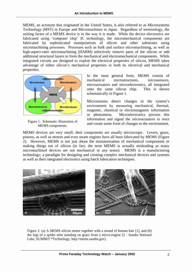
In the most general form, MEMS consist of mechanical microstructures, microsensors, microactuators and microelectronics, all integrated onto the same silicon chip. This is shown schematically in Figure 1.
Microsensors detect changes in the system’s environment by measuring mechanical, thermal, magnetic, chemical or electromagnetic information or phenomena. Microelectronics process this information and signal the microactuators to react and create some form of changes to the environment.
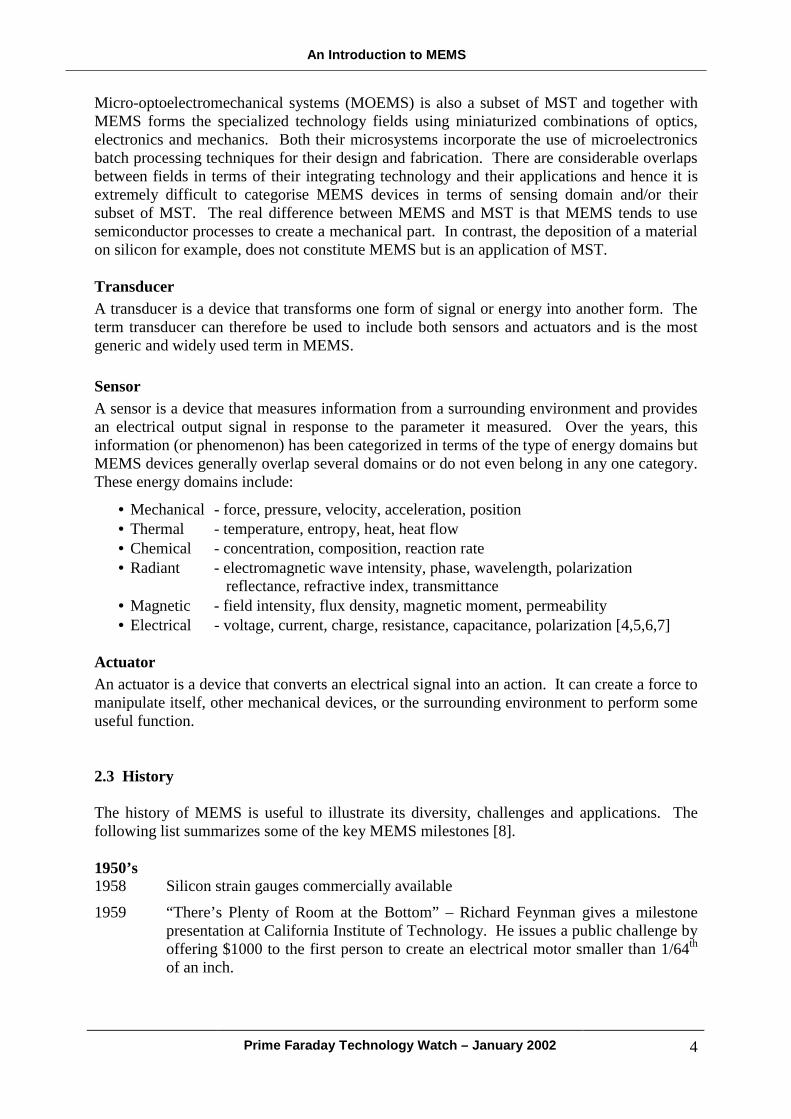
MEMS devices are very small; their components are usually microscopic. Levers, gears, pistons, as well as motors and even steam engines have all been fabricated by MEMS (Figure 2). However, MEMS is not just about the miniaturization of mechanical components or making things out of silicon (in fact, the term MEMS is actually misleading as many micromachined devices are not mechanical in any sense). MEMS is a manufacturing technology; a paradigm for designing and creating complex mechanical devices and systems as well as their integrated electronics using batch fabrication techniques.
Figure 1. Schematic illustration of MEMS components.
Figure 2. (a) A MEMS silicon motor together with a strand of human hair [1], and (b) the legs of a spider mite standing on gears from a micro-engine [2 - Sandia National Labs, SUMMiT *Technology, http://mems.sandia.gov].

An Introduction to MEMS
Prime Faraday Technology Watch – January 2002 3
From a very early vision in the early 1950’s, MEMS has gradually made its way out of research laboratories and into everyday products. In the mid-1990’s, MEMS components began appearing in numerous commercial products and applications including accelerometers used to control airbag deployment in vehicles, pressure sensors for medical applications, and inkjet printer heads. Today, MEMS devices are also found in projection displays and for micropositioners in data storage systems. However, the greatest potential for MEMS devices lies in new applications within telecommunications (optical and wireless), biomedical and process control areas. MEMS has several distinct advantages as a manufacturing technology. In the first place, the interdisciplinary nature of MEMS technology and its micromachining techniques, as well as its diversity of applications has resulted in an unprecedented range of devices and synergies across previously unrelated fields (for example biology and microelectronics). Secondly, MEMS with its batch fabrication techniques enables components and devices to be manufactured with increased performance and reliability, combined with the obvious advantages of reduced physical size, volume, weight and cost. Thirdly, MEMS provides the basis for the manufacture of products that cannot be made by other methods. These factors make MEMS potentially a far more pervasive technology than integrated circuit microchips. However, there are many challenges and technological obstacles associated with miniaturization that need to be addressed and overcome before MEMS can realize its overwhelming potential. 2.2 Definitions and Classifications This section defines some of the key terminology and classifications associated with MEMS. It is intended to help the reader and newcomers to the field of micromachining become familiar with some of the more common terms. A more detailed glossary of terms has been included in Appendix A. Figure 3 illustrates the classifications of microsystems technology (MST). Although MEMS is also referred to as MST, strictly speaking, MEMS is a process technology used to create these tiny mechanical devices or systems, and as a result, it is a subset of MST.
Figure 3. Classifications of microsystems technology [3].
An Introduction to MEMS
Prime Faraday Technology Watch – January 2002 4
Micro-optoelectromechanical systems (MOEMS) is also a subset of MST and together with MEMS forms the specialized technology fields using miniaturized combinations of optics, electronics and mechanics. Both their microsystems incorporate the use of microelectronics batch processing techniques for their design and fabrication. There are considerable overlaps between fields in terms of their integrating technology and their applications and hence it is extremely difficult to categorise MEMS devices in terms of sensing domain and/or their subset of MST. The real difference between MEMS and MST is that MEMS tends to use semiconductor processes to create a mechanical part. In contrast, the deposition of a material on silicon for example, does not constitute MEMS but is an application of MST. Transducer A transducer is a device that transforms one form of signal or energy into another form. The term transducer can therefore be used to include both sensors and actuators and is the most generic and widely used term in MEMS. Sensor A sensor is a device that measures information from a surrounding environment and provides an electrical output signal in response to the parameter it measured. Over the years, this information (or phenomenon) has been categorized in terms of the type of energy domains but MEMS devices generally overlap several domains or do not even belong in any one category. These energy domains include:
• Mechanical - force, pressure, velocity, acceleration, position • Thermal - temperature, entropy, heat, heat flow • Chemical - concentration, composition, reaction rate • Radiant - electromagnetic wave intensity, phase, wavelength, polarization
reflectance, refractive index, transmittance • Magnetic - field intensity, flux density, magnetic moment, permeability • Electrical - voltage, current, charge, resistance, capacitance, polarization [4,5,6,7]
Actuator An actuator is a device that converts an electrical signal into an action. It can create a force to manipulate itself, other mechanical devices, or the surrounding environment to perform some useful function. 2.3 History The history of MEMS is useful to illustrate its diversity, challenges and applications. The following list summarizes some of the key MEMS milestones [8]. 1950’s 1958 Silicon strain gauges commercially available 1959 “There’s Plenty of Room at the Bottom” – Richard Feynman gives a milestone
presentation at California Institute of Technology. He issues a public challenge by offering $1000 to the first person to create an electrical motor smaller than 1/64th of an inch.
An Introduction to MEMS
Prime Faraday Technology Watch – January 2002 5
1960’s 1961 First silicon pressure sensor demonstrated 1967 Invention of surface micromachining. Westinghouse creates the Resonant Gate
Field Effect Transistor, (RGT). Description of use of sacrificial material to free micromechanical devices from the silicon substrate.
1970’s 1970 First silicon accelerometer demonstrated 1979 First micromachined inkjet nozzle 1980’s
Early 1980’s: first experiments in surface micromachined silicon. Late 1980’s: micromachining leverages microelectronics industry and widespread experimentation and documentation increases public interest.
1982 Disposable blood pressure transducer 1982 “Silicon as a Mechanical Material” [9]. Instrumental paper to entice the scientific
community – reference for material properties and etching data for silicon. 1982 LIGA Process 1988 First MEMS conference 1990’s Methods of micromachining aimed towards improving sensors. 1992 MCNC starts the Multi-User MEMS Process (MUMPS) sponsored by Defense
Advanced Research Projects Agency (DARPA) 1992 First micromachined hinge 1993 First surface micromachined accelerometer sold (Analog Devices, ADXL50) 1994 Deep Reactive Ion Etching is patented 1995 BioMEMS rapidly develops 2000 MEMS optical-networking components become big business
An Introduction to MEMS
Prime Faraday Technology Watch – January 2002 6
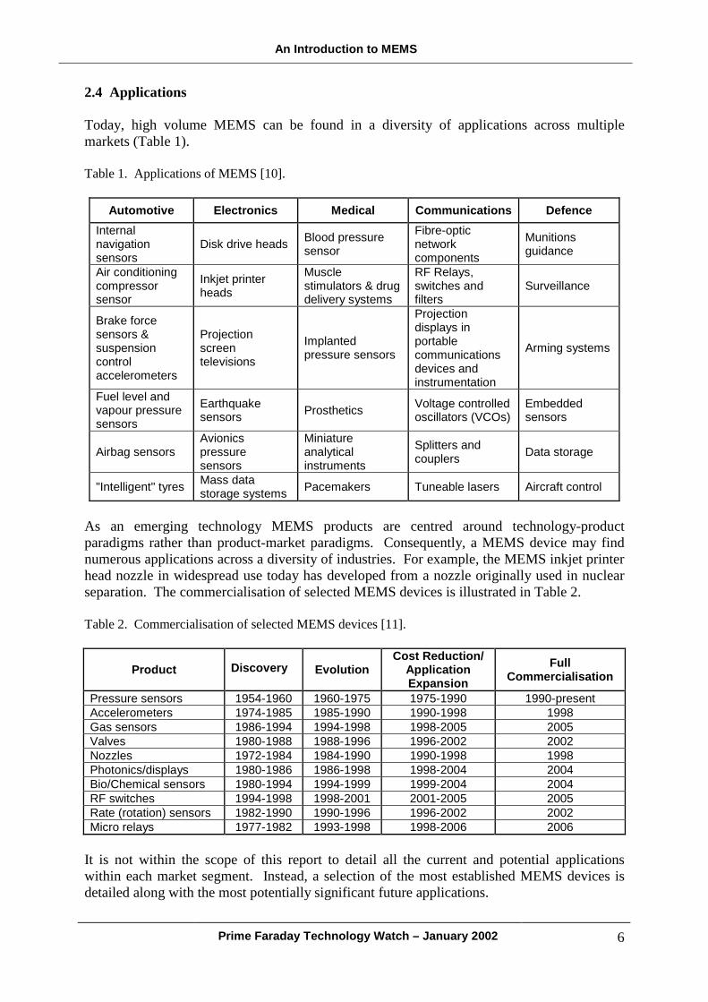
2.4 Applications Today, high volume MEMS can be found in a diversity of applications across multiple markets (Table 1). Table 1. Applications of MEMS [10].
Automotive Electronics Medical Communications Defence Internal navigation sensors
Disk drive heads Blood pressure sensor
Fibre-optic network components
Munitions guidance
Air conditioning compressor sensor
Inkjet printer heads
Muscle stimulators & drug delivery systems
RF Relays, switches and filters
Surveillance
Brake force sensors & suspension control accelerometers
Projection screen televisions
Implanted pressure sensors
Projection displays in portable communications devices and instrumentation
Arming systems
Fuel level and vapour pressure sensors
Earthquake sensors Prosthetics Voltage controlled
oscillators (VCOs) Embedded sensors
Airbag sensors Avionics pressure sensors
Miniature analytical instruments
Splitters and couplers Data storage
"Intelligent" tyres Mass data storage systems Pacemakers Tuneable lasers Aircraft control
As an emerging technology MEMS products are centred around technology-product paradigms rather than product-market paradigms. Consequently, a MEMS device may find numerous applications across a diversity of industries. For example, the MEMS inkjet printer head nozzle in widespread use today has developed from a nozzle originally used in nuclear separation. The commercialisation of selected MEMS devices is illustrated in Table 2. Table 2. Commercialisation of selected MEMS devices [11].
Product Discovery Evolution Cost Reduction/
Application Expansion
Full Commercialisation
Pressure sensors 1954-1960 1960-1975 1975-1990 1990-present Accelerometers 1974-1985 1985-1990 1990-1998 1998 Gas sensors 1986-1994 1994-1998 1998-2005 2005 Valves 1980-1988 1988-1996 1996-2002 2002 Nozzles 1972-1984 1984-1990 1990-1998 1998 Photonics/displays 1980-1986 1986-1998 1998-2004 2004 Bio/Chemical sensors 1980-1994 1994-1999 1999-2004 2004 RF switches 1994-1998 1998-2001 2001-2005 2005 Rate (rotation) sensors 1982-1990 1990-1996 1996-2002 2002 Micro relays 1977-1982 1993-1998 1998-2006 2006
It is not within the scope of this report to detail all the current and potential applications within each market segment. Instead, a selection of the most established MEMS devices is detailed along with the most potentially significant future applications.
An Introduction to MEMS
Prime Faraday Technology Watch – January 2002 7
2.4.1 Established MEMS Applications i) Automotive airbag sensor
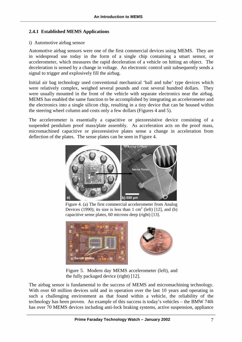
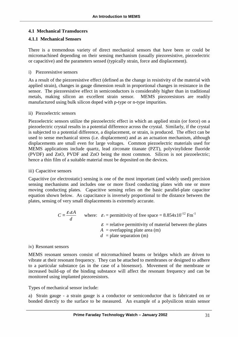
Automotive airbag sensors were one of the first commercial devices using MEMS. They are in widespread use today in the form of a single chip containing a smart sensor, or accelerometer, which measures the rapid deceleration of a vehicle on hitting an object. The deceleration is sensed by a change in voltage. An electronic control unit subsequently sends a signal to trigger and explosively fill the airbag. Initial air bag technology used conventional mechanical ‘ball and tube’ type devices which were relatively complex, weighed several pounds and cost several hundred dollars. They were usually mounted in the front of the vehicle with separate electronics near the airbag. MEMS has enabled the same function to be accomplished by integrating an accelerometer and the electronics into a single silicon chip, resulting in a tiny device that can be housed within the steering wheel column and costs only a few dollars (Figures 4 and 5). The accelerometer is essentially a capacitive or piezoresistive device consisting of a suspended pendulum proof mass/plate assembly. As acceleration acts on the proof mass, micromachined capacitive or piezoresistive plates sense a change in acceleration from deflection of the plates. The sense plates can be seen in Figure 4.
The airbag sensor is fundamental to the success of MEMS and micromachining technology. With over 60 million devices sold and in operation over the last 10 years and operating in such a challenging environment as that found within a vehicle, the reliability of the technology has been proven. An example of this success is today’s vehicles – the BMW 740i has over 70 MEMS devices including anti-lock braking systems, active suspension, appliance
Figure 4. (a) The first commercial accelerometer from Analog Devices (1990); its size is less than 1 cm2 (left) [12], and (b) capacitive sense plates, 60 microns deep (right) [13].
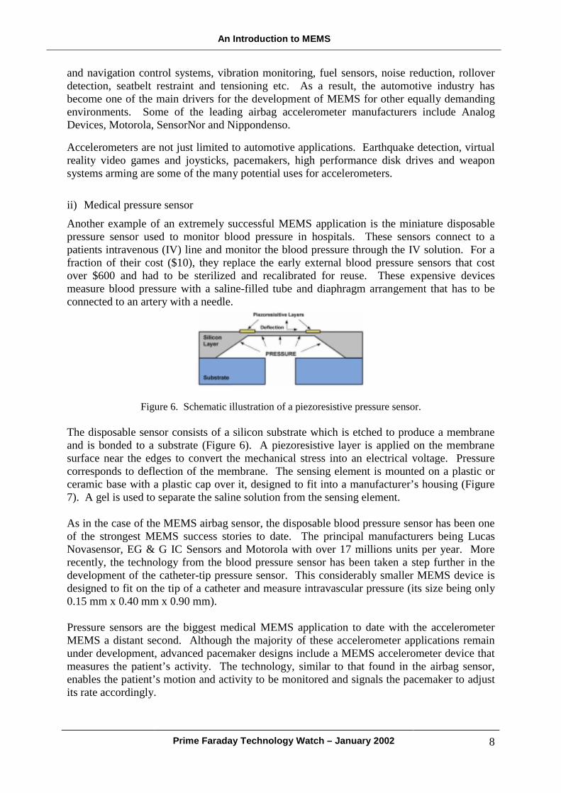
Figure 5. Modern day MEMS accelerometer (left), and the fully packaged device (right) [12].
An Introduction to MEMS
Prime Faraday Technology Watch – January 2002 8
and navigation control systems, vibration monitoring, fuel sensors, noise reduction, rollover detection, seatbelt restraint and tensioning etc. As a result, the automotive industry has become one of the main drivers for the development of MEMS for other equally demanding environments. Some of the leading airbag accelerometer manufacturers include Analog Devices, Motorola, SensorNor and Nippondenso. Accelerometers are not just limited to automotive applications. Earthquake detection, virtual reality video games and joysticks, pacemakers, high performance disk drives and weapon systems arming are some of the many potential uses for accelerometers.
ii) Medical pressure sensor
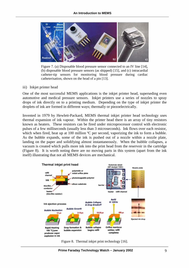
Another example of an extremely successful MEMS application is the miniature disposable pressure sensor used to monitor blood pressure in hospitals. These sensors connect to a patients intravenous (IV) line and monitor the blood pressure through the IV solution. For a fraction of their cost ($10), they replace the early external blood pressure sensors that cost over $600 and had to be sterilized and recalibrated for reuse. These expensive devices measure blood pressure with a saline-filled tube and diaphragm arrangement that has to be connected to an artery with a needle.
Figure 6. Schematic illustration of a piezoresistive pressure sensor.
The disposable sensor consists of a silicon substrate which is etched to produce a membrane and is bonded to a substrate (Figure 6). A piezoresistive layer is applied on the membrane surface near the edges to convert the mechanical stress into an electrical voltage. Pressure corresponds to deflection of the membrane. The sensing element is mounted on a plastic or ceramic base with a plastic cap over it, designed to fit into a manufacturer’s housing (Figure 7). A gel is used to separate the saline solution from the sensing element. As in the case of the MEMS airbag sensor, the disposable blood pressure sensor has been one of the strongest MEMS success stories to date. The principal manufacturers being Lucas Novasensor, EG & G IC Sensors and Motorola with over 17 millions units per year. More recently, the technology from the blood pressure sensor has been taken a step further in the development of the catheter-tip pressure sensor. This considerably smaller MEMS device is designed to fit on the tip of a catheter and measure intravascular pressure (its size being only 0.15 mm x 0.40 mm x 0.90 mm). Pressure sensors are the biggest medical MEMS application to date with the accelerometer MEMS a distant second. Although the majority of these accelerometer applications remain under development, advanced pacemaker designs include a MEMS accelerometer device that measures the patient’s activity. The technology, similar to that found in the airbag sensor, enables the patient’s motion and activity to be monitored and signals the pacemaker to adjust its rate accordingly.
An Introduction to MEMS
Prime Faraday Technology Watch – January 2002 9
iii) Inkjet printer head
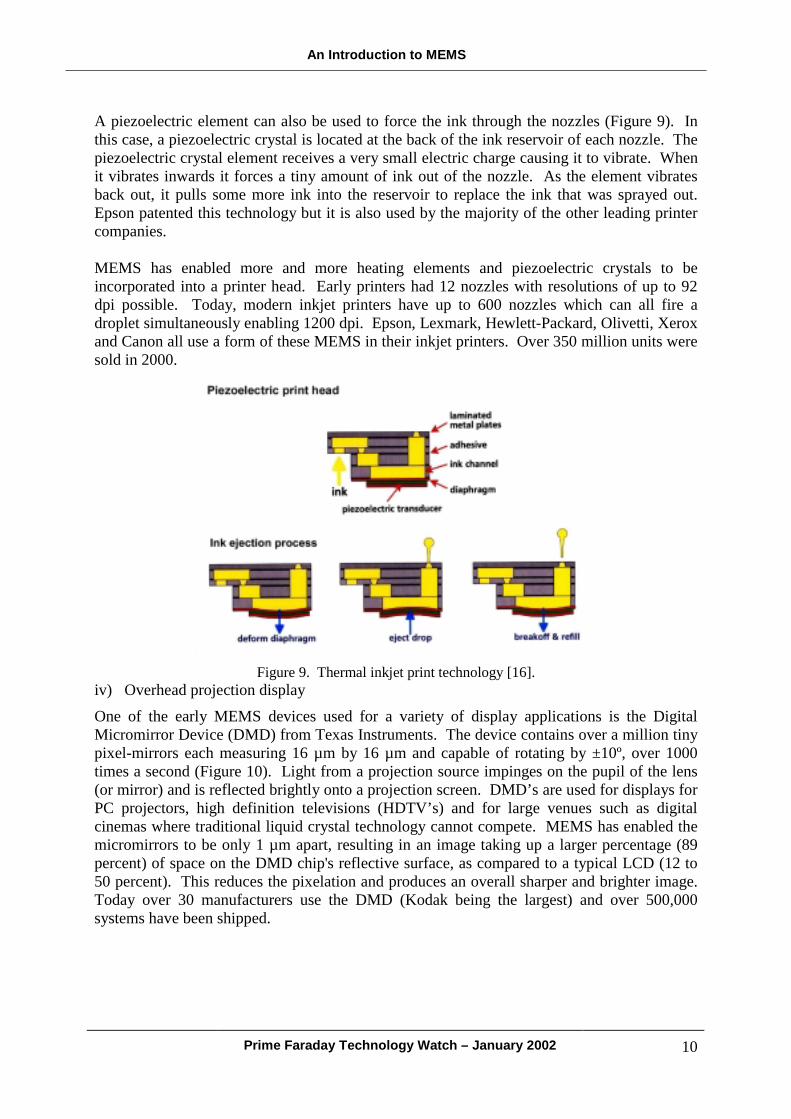
One of the most successful MEMS applications is the inkjet printer head, superseding even automotive and medical pressure sensors. Inkjet printers use a series of nozzles to spray drops of ink directly on to a printing medium. Depending on the type of inkjet printer the droplets of ink are formed in different ways; thermally or piezoelectrically. Invented in 1979 by Hewlett-Packard, MEMS thermal inkjet printer head technology uses thermal expansion of ink vapour. Within the printer head there is an array of tiny resistors known as heaters. These resistors can be fired under microprocessor control with electronic pulses of a few milliseconds (usually less than 3 microseconds). Ink flows over each resistor, which when fired, heat up at 100 million ºC per second, vaporizing the ink to form a bubble. As the bubble expands, some of the ink is pushed out of a nozzle within a nozzle plate, landing on the paper and solidifying almost instantaneously. When the bubble collapses, a vacuum is created which pulls more ink into the print head from the reservoir in the cartridge (Figure 8). It is worth noting there are no moving parts in this system (apart from the ink itself) illustrating that not all MEMS devices are mechanical.
Figure 8. Thermal inkjet print technology [16].
Figure 7. (a) Disposable blood pressure sensor connected to an IV line [14], (b) disposable blood pressure sensors (as shipped) [15], and (c) intracardial catheter-tip sensors for monitoring blood pressure during cardiac catheterisation, shown on the head of a pin [13].
An Introduction to MEMS
Prime Faraday Technology Watch – January 2002 10
A piezoelectric element can also be used to force the ink through the nozzles (Figure 9). In this case, a piezoelectric crystal is located at the back of the ink reservoir of each nozzle. The piezoelectric crystal element receives a very small electric charge causing it to vibrate. When it vibrates inwards it forces a tiny amount of ink out of the nozzle. As the element vibrates back out, it pulls some more ink into the reservoir to replace the ink that was sprayed out. Epson patented this technology but it is also used by the majority of the other leading printer companies. MEMS has enabled more and more heating elements and piezoelectric crystals to be incorporated into a printer head. Early printers had 12 nozzles with resolutions of up to 92 dpi possible. Today, modern inkjet printers have up to 600 nozzles which can all fire a droplet simultaneously enabling 1200 dpi. Epson, Lexmark, Hewlett-Packard, Olivetti, Xerox and Canon all use a form of these MEMS in their inkjet printers. Over 350 million units were sold in 2000.
Figure 9. Thermal inkjet print technology [16].
iv) Overhead projection display
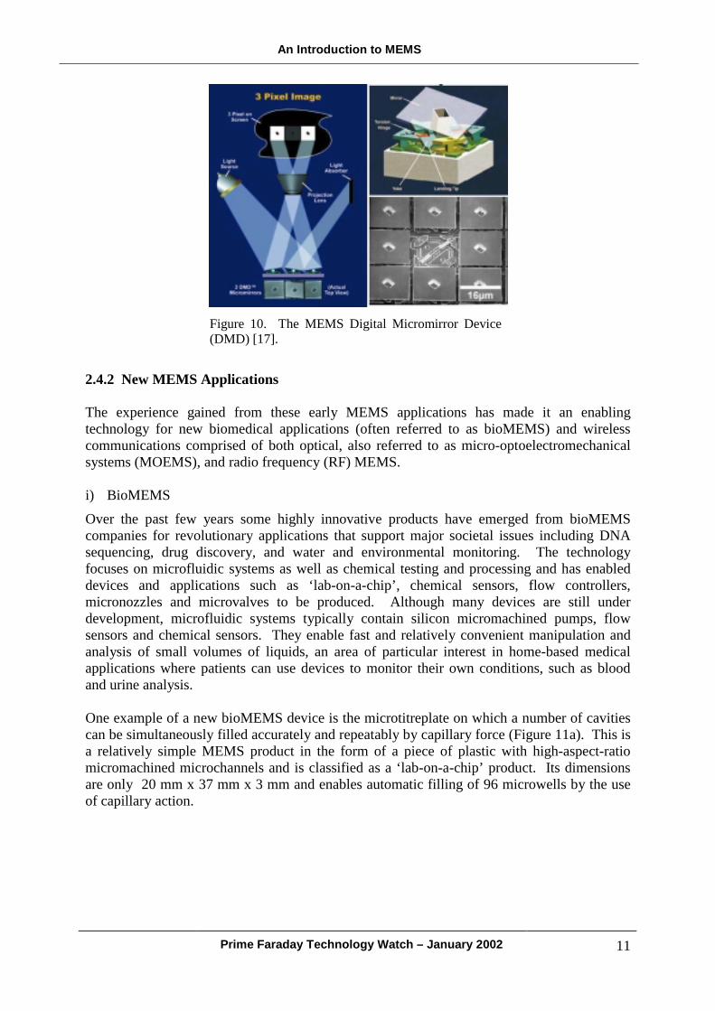
One of the early MEMS devices used for a variety of display applications is the Digital Micromirror Device (DMD) from Texas Instruments. The device contains over a million tiny pixel-mirrors each measuring 16 µm by 16 µm and capable of rotating by ±10º, over 1000 times a second (Figure 10). Light from a projection source impinges on the pupil of the lens (or mirror) and is reflected brightly onto a projection screen. DMD’s are used for displays for PC projectors, high definition televisions (HDTV’s) and for large venues such as digital cinemas where traditional liquid crystal technology cannot compete. MEMS has enabled the micromirrors to be only 1 µm apart, resulting in an image taking up a larger percentage (89 percent) of space on the DMD chip's reflective surface, as compared to a typical LCD (12 to 50 percent). This reduces the pixelation and produces an overall sharper and brighter image. Today over 30 manufacturers use the DMD (Kodak being the largest) and over 500,000 systems have been shipped.
An Introduction to MEMS
Prime Faraday Technology Watch – January 2002 11
2.4.2 New MEMS Applications The experience gained from these early MEMS applications has made it an enabling technology for new biomedical applications (often referred to as bioMEMS) and wireless communications comprised of both optical, also referred to as micro-optoelectromechanical systems (MOEMS), and radio frequency (RF) MEMS. i) BioMEMS
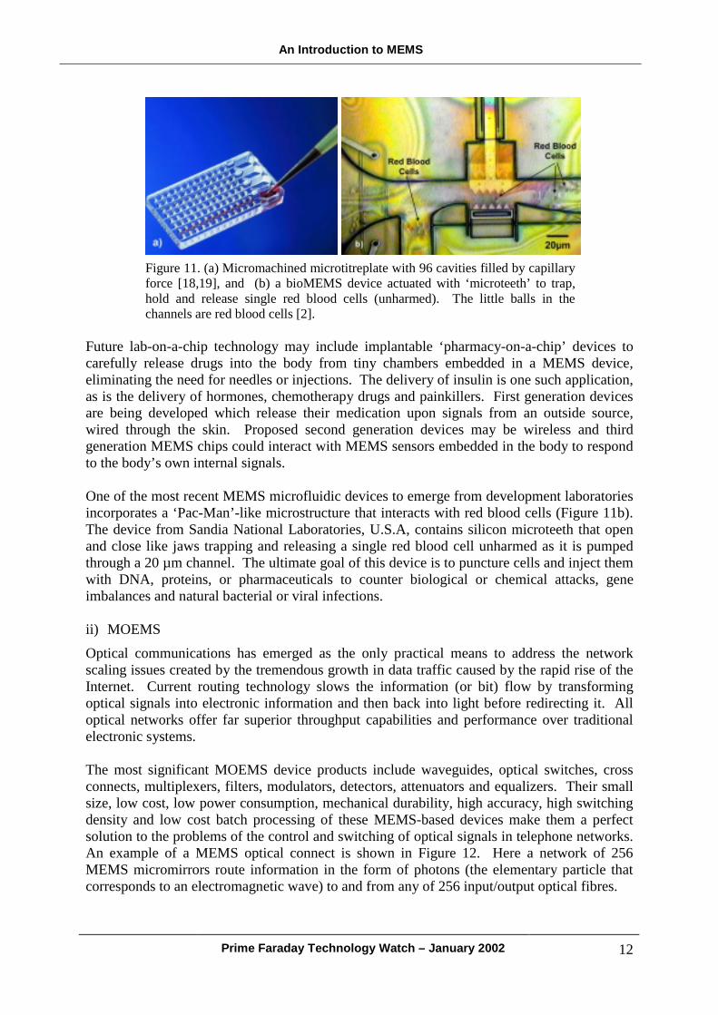
Over the past few years some highly innovative products have emerged from bioMEMS companies for revolutionary applications that support major societal issues including DNA sequencing, drug discovery, and water and environmental monitoring. The technology focuses on microfluidic systems as well as chemical testing and processing and has enabled devices and applications such as ‘lab-on-a-chip’, chemical sensors, flow controllers, micronozzles and microvalves to be produced. Although many devices are still under development, microfluidic systems typically contain silicon micromachined pumps, flow sensors and chemical sensors. They enable fast and relatively convenient manipulation and analysis of small volumes of liquids, an area of particular interest in home-based medical applications where patients can use devices to monitor their own conditions, such as blood and urine analysis. One example of a new bioMEMS device is the microtitreplate on which a number of cavities can be simultaneously filled accurately and repeatably by capillary force (Figure 11a). This is a relatively simple MEMS product in the form of a piece of plastic with high-aspect-ratio micromachined microchannels and is classified as a ‘lab-on-a-chip’ product. Its dimensions are only 20 mm x 37 mm x 3 mm and enables automatic filling of 96 microwells by the use of capillary action.
Figure 10. The MEMS Digital Micromirror Device (DMD) [17].
An Introduction to MEMS
Prime Faraday Technology Watch – January 2002 12
Future lab-on-a-chip technology may include implantable ‘pharmacy-on-a-chip’ devices to carefully release drugs into the body from tiny chambers embedded in a MEMS device, eliminating the need for needles or injections. The delivery of insulin is one such application, as is the delivery of hormones, chemotherapy drugs and painkillers. First generation devices are being developed which release their medication upon signals from an outside source, wired through the skin. Proposed second generation devices may be wireless and third generation MEMS chips could interact with MEMS sensors embedded in the body to respond to the body’s own internal signals. One of the most recent MEMS microfluidic devices to emerge from development laboratories incorporates a ‘Pac-Man’-like microstructure that interacts with red blood cells (Figure 11b). The device from Sandia National Laboratories, U.S.A, contains silicon microteeth that open and close like jaws trapping and releasing a single red blood cell unharmed as it is pumped through a 20 µm channel. The ultimate goal of this device is to puncture cells and inject them with DNA, proteins, or pharmaceuticals to counter biological or chemical attacks, gene imbalances and natural bacterial or viral infections. ii) MOEMS
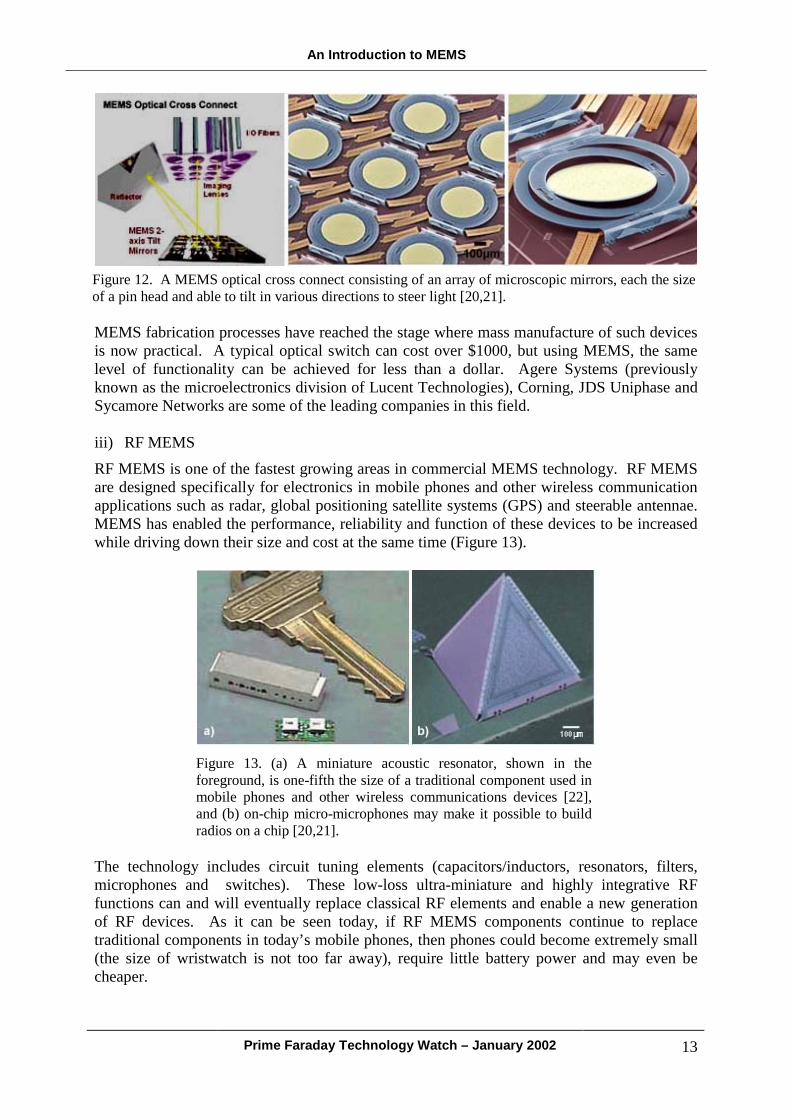
Optical communications has emerged as the only practical means to address the network scaling issues created by the tremendous growth in data traffic caused by the rapid rise of the Internet. Current routing technology slows the information (or bit) flow by transforming optical signals into electronic information and then back into light before redirecting it. All optical networks offer far superior throughput capabilities and performance over traditional electronic systems. The most significant MOEMS device products include waveguides, optical switches, cross connects, multiplexers, filters, modulators, detectors, attenuators and equalizers. Their small size, low cost, low power consumption, mechanical durability, high accuracy, high switching density and low cost batch processing of these MEMS-based devices make them a perfect solution to the problems of the control and switching of optical signals in telephone networks. An example of a MEMS optical connect is shown in Figure 12. Here a network of 256 MEMS micromirrors route information in the form of photons (the elementary particle that corresponds to an electromagnetic wave) to and from any of 256 input/output optical fibres.
Figure 11. (a) Micromachined microtitreplate with 96 cavities filled by capillary force [18,19], and (b) a bioMEMS device actuated with ‘microteeth’ to trap, hold and release single red blood cells (unharmed). The little balls in the channels are red blood cells [2].
An Introduction to MEMS
Prime Faraday Technology Watch – January 2002 13
MEMS fabrication processes have reached the stage where mass manufacture of such devices is now practical. A typical optical switch can cost over $1000, but using MEMS, the same level of functionality can be achieved for less than a dollar. Agere Systems (previously known as the microelectronics division of Lucent Technologies), Corning, JDS Uniphase and Sycamore Networks are some of the leading companies in this field. iii) RF MEMS
RF MEMS is one of the fastest growing areas in commercial MEMS technology. RF MEMS are designed specifically for electronics in mobile phones and other wireless communication applications such as radar, global positioning satellite systems (GPS) and steerable antennae. MEMS has enabled the performance, reliability and function of these devices to be increased while driving down their size and cost at the same time (Figure 13).
The technology includes circuit tuning elements (capacitors/inductors, resonators, filters, microphones and switches). These low-loss ultra-miniature and highly integrative RF functions can and will eventually replace classical RF elements and enable a new generation of RF devices. As it can be seen today, if RF MEMS components continue to replace traditional components in today’s mobile phones, then phones could become extremely small (the size of wristwatch is not too far away), require little battery power and may even be cheaper.
Figure 12. A MEMS optical cross connect consisting of an array of microscopic mirrors, each the size of a pin head and able to tilt in various directions to steer light [20,21].
Figure 13. (a) A miniature acoustic resonator, shown in the foreground, is one-fifth the size of a traditional component used in mobile phones and other wireless communications devices [22], and (b) on-chip micro-microphones may make it possible to build radios on a chip [20,21].
An Introduction to MEMS
Prime Faraday Technology Watch – January 2002 14
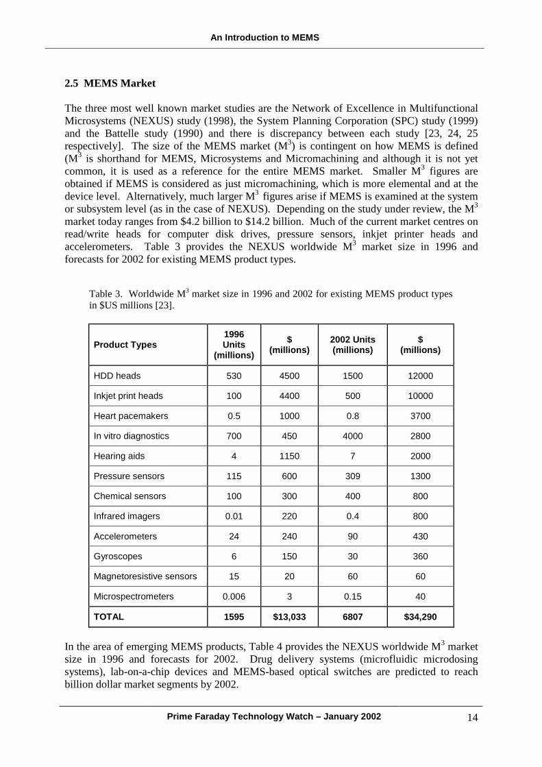
2.5 MEMS Market The three most well known market studies are the Network of Excellence in Multifunctional Microsystems (NEXUS) study (1998), the System Planning Corporation (SPC) study (1999) and the Battelle study (1990) and there is discrepancy between each study [23, 24, 25 respectively]. The size of the MEMS market (M3) is contingent on how MEMS is defined (M3 is shorthand for MEMS, Microsystems and Micromachining and although it is not yet common, it is used as a reference for the entire MEMS market. Smaller M3 figures are obtained if MEMS is considered as just micromachining, which is more elemental and at the device level. Alternatively, much larger M3 figures arise if MEMS is examined at the system or subsystem level (as in the case of NEXUS). Depending on the study under review, the M3 market today ranges from $4.2 billion to $14.2 billion. Much of the current market centres on read/write heads for computer disk drives, pressure sensors, inkjet printer heads and accelerometers. Table 3 provides the NEXUS worldwide M3 market size in 1996 and forecasts for 2002 for existing MEMS product types.
Product Types 1996 Units
(millions) $
(millions) 2002 Units (millions)
$ (millions)
HDD heads 530 4500 1500 12000
Inkjet print heads 100 4400 500 10000
Heart pacemakers 0.5 1000 0.8 3700
In vitro diagnostics 700 450 4000 2800
Hearing aids 4 1150 7 2000
Pressure sensors 115 600 309 1300
Chemical sensors 100 300 400 800
Infrared imagers 0.01 220 0.4 800
Accelerometers 24 240 90 430
Gyroscopes 6 150 30 360
Magnetoresistive sensors 15 20 60 60
Microspectrometers 0.006 3 0.15 40
TOTAL 1595 $13,033 6807 $34,290
In the area of emerging MEMS products, Table 4 provides the NEXUS worldwide M3 market size in 1996 and forecasts for 2002. Drug delivery systems (microfluidic microdosing systems), lab-on-a-chip devices and MEMS-based optical switches are predicted to reach billion dollar market segments by 2002.
Table 3. Worldwide M3 market size in 1996 and 2002 for existing MEMS product types in $US millions [23].
An Introduction to MEMS
Prime Faraday Technology Watch – January 2002 15
Product Types 1996 Units
(millions) $
(millions) 2002 Units (millions) $ (millions)
Drug delivery systems 1 10 100 1000 Optical switches 1 50 40 1000 Lab on ship 0 0 100 1000 Magneto optical heads 0.01 1 100 500 Projection valves 0.1 10 1 300 Coil on chip 20 10 600 100 Micro relays 0.1 50 100 Micromotors 0.1 5 2 80 Inclinometers 1 10 20 70 Injection nozzles 10 10 30 30 Anti-collision sensors 0.01 0.5 2 20 Electronic noses 0.001 0.1 0.05 5 TOTAL 33 $107 1045 $4,205
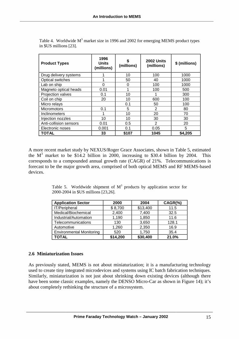
A more recent market study by NEXUS/Roger Grace Associates, shown in Table 5, estimated the M3 market to be $14.2 billion in 2000, increasing to $30.4 billion by 2004. This corresponds to a compounded annual growth rate (CAGR) of 21%. Telecommunications is forecast to be the major growth area, comprised of both optical MEMS and RF MEMS-based devices.
Application Sector 2000 2004 CAGR(%) IT/Peripheral $ 8,700 $13,400 11.5 Medical/Biochemical 2,400 7,400 32.5 Industrial/Automation 1,190 1,850 11.6 Telecommunications 130 3,650 128.1 Automotive 1,260 2,350 16.9 Environmental Monitoring 520 1,750 35.4 TOTAL $14,200 $30,400 21.0%
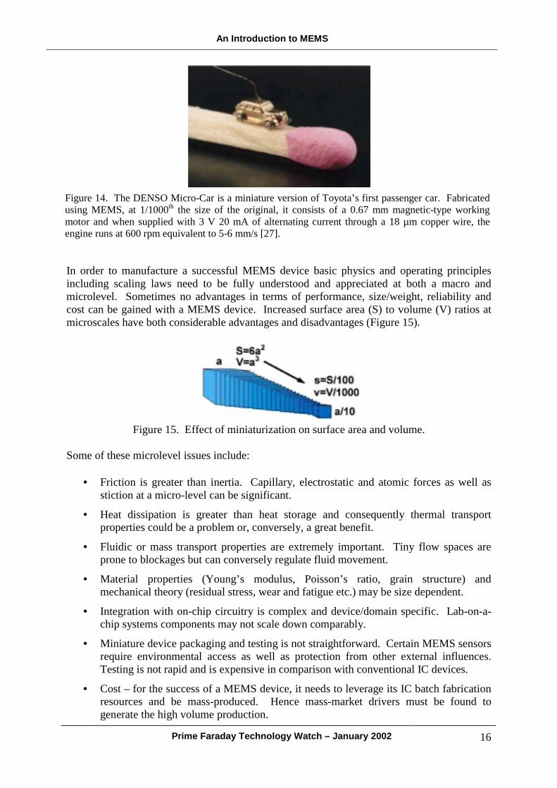
2.6 Miniaturization Issues As previously stated, MEMS is not about miniaturization; it is a manufacturing technology used to create tiny integrated microdevices and systems using IC batch fabrication techniques. Similarly, miniaturization is not just about shrinking down existing devices (although there have been some classic examples, namely the DENSO Micro-Car as shown in Figure 14); it’s about completely rethinking the structure of a microsystem.
Table 4. Worldwide M3 market size in 1996 and 2002 for emerging MEMS product types in $US millions [23].
Table 5. Worldwide shipment of M3 products by application sector for 2000-2004 in $US millions [23,26].
An Introduction to MEMS
Prime Faraday Technology Watch – January 2002 16
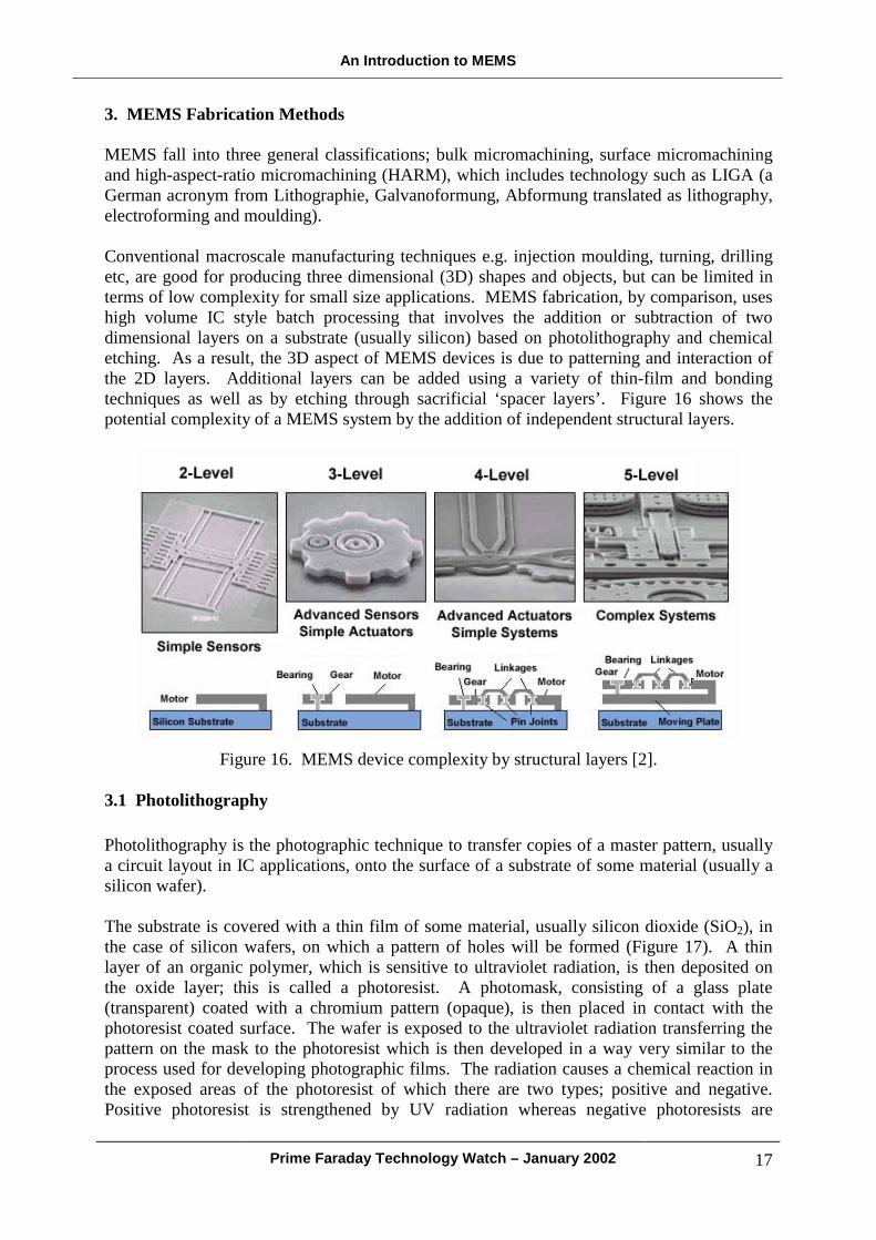
In order to manufacture a successful MEMS device basic physics and operating principles including scaling laws need to be fully understood and appreciated at both a macro and microlevel. Sometimes no advantages in terms of performance, size/weight, reliability and cost can be gained with a MEMS device. Increased surface area (S) to volume (V) ratios at microscales have both considerable advantages and disadvantages (Figure 15).
Figure 15. Effect of miniaturization on surface area and volume.
Some of these microlevel issues include:
• Friction is greater than inertia. Capillary, electrostatic and atomic forces as well as stiction at a micro-level can be significant.
• Heat dissipation is greater than heat storage and consequently thermal transport properties could be a problem or, conversely, a great benefit.
• Fluidic or mass transport properties are extremely important. Tiny flow spaces are prone to blockages but can conversely regulate fluid movement.
• Material properties (Young’s modulus, Poisson’s ratio, grain structure) and mechanical theory (residual stress, wear and fatigue etc.) may be size dependent.
• Integration with on-chip circuitry is complex and device/domain specific. Lab-on-a-chip systems components may not scale down comparably.
• Miniature device packaging and testing is not straightforward. Certain MEMS sensors require environmental access as well as protection from other external influences. Testing is not rapid and is expensive in comparison with conventional IC devices.
• Cost – for the success of a MEMS device, it needs to leverage its IC batch fabrication resources and be mass-produced. Hence mass-market drivers must be found to generate the high volume production.
Figure 14. The DENSO Micro-Car is a miniature version of Toyota’s first passenger car. Fabricated using MEMS, at 1/1000th the size of the original, it consists of a 0.67 mm magnetic-type working motor and when supplied with 3 V 20 mA of alternating current through a 18 µm copper wire, the engine runs at 600 rpm equivalent to 5-6 mm/s [27].
An Introduction to MEMS
Prime Faraday Technology Watch – January 2002 17
3. MEMS Fabrication Methods MEMS fall into three general classifications; bulk micromachining, surface micromachining and high-aspect-ratio micromachining (HARM), which includes technology such as LIGA (a German acronym from Lithographie, Galvanoformung, Abformung translated as lithography, electroforming and moulding). Conventional macroscale manufacturing techniques e.g. injection moulding, turning, drilling etc, are good for producing three dimensional (3D) shapes and objects, but can be limited in terms of low complexity for small size applications. MEMS fabrication, by comparison, uses high volume IC style batch processing that involves the addition or subtraction of two dimensional layers on a substrate (usually silicon) based on photolithography and chemical etching. As a result, the 3D aspect of MEMS devices is due to patterning and interaction of the 2D layers. Additional layers can be added using a variety of thin-film and bonding techniques as well as by etching through sacrificial ‘spacer layers’. Figure 16 shows the potential complexity of a MEMS system by the addition of independent structural layers.
Figure 16. MEMS device complexity by structural layers [2].
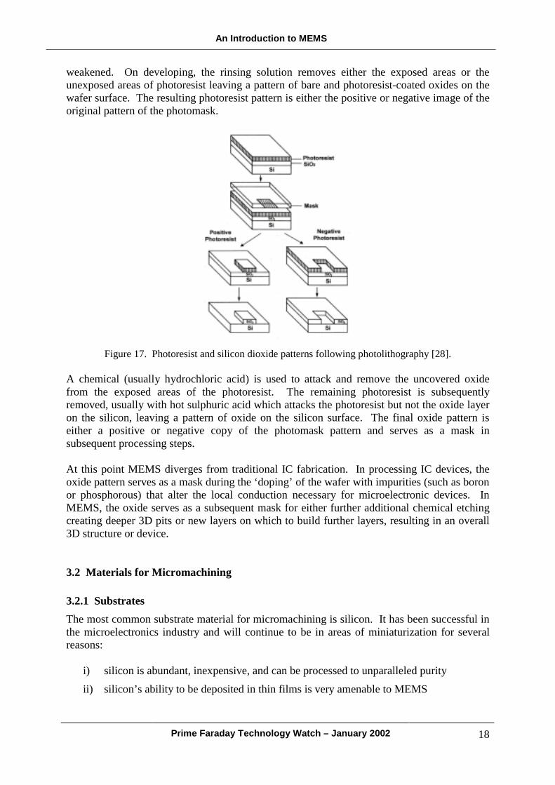
3.1 Photolithography Photolithography is the photographic technique to transfer copies of a master pattern, usually a circuit layout in IC applications, onto the surface of a substrate of some material (usually a silicon wafer). The substrate is covered with a thin film of some material, usually silicon dioxide (SiO2), in the case of silicon wafers, on which a pattern of holes will be formed (Figure 17). A thin layer of an organic polymer, which is sensitive to ultraviolet radiation, is then deposited on the oxide layer; this is called a photoresist. A photomask, consisting of a glass plate (transparent) coated with a chromium pattern (opaque), is then placed in contact with the photoresist coated surface. The wafer is exposed to the ultraviolet radiation transferring the pattern on the mask to the photoresist which is then developed in a way very similar to the process used for developing photographic films. The radiation causes a chemical reaction in the exposed areas of the photoresist of which there are two types; positive and negative. Positive photoresist is strengthened by UV radiation whereas negative photoresists are
An Introduction to MEMS
Prime Faraday Technology Watch – January 2002 18
weakened. On developing, the rinsing solution removes either the exposed areas or the unexposed areas of photoresist leaving a pattern of bare and photoresist-coated oxides on the wafer surface. The resulting photoresist pattern is either the positive or negative image of the original pattern of the photomask.
Figure 17. Photoresist and silicon dioxide patterns following photolithography [28].
A chemical (usually hydrochloric acid) is used to attack and remove the uncovered oxide from the exposed areas of the photoresist. The remaining photoresist is subsequently removed, usually with hot sulphuric acid which attacks the photoresist but not the oxide layer on the silicon, leaving a pattern of oxide on the silicon surface. The final oxide pattern is either a positive or negative copy of the photomask pattern and serves as a mask in subsequent processing steps. At this point MEMS diverges from traditional IC fabrication. In processing IC devices, the oxide pattern serves as a mask during the ‘doping’ of the wafer with impurities (such as boron or phosphorous) that alter the local conduction necessary for microelectronic devices. In MEMS, the oxide serves as a subsequent mask for either further additional chemical etching creating deeper 3D pits or new layers on which to build further layers, resulting in an overall 3D structure or device. 3.2 Materials for Micromachining 3.2.1 Substrates The most common substrate material for micromachining is silicon. It has been successful in the microelectronics industry and will continue to be in areas of miniaturization for several reasons:
i) silicon is abundant, inexpensive, and can be processed to unparalleled purity ii) silicon’s ability to be deposited in thin films is very amenable to MEMS
An Introduction to MEMS
Prime Faraday Technology Watch – January 2002 19
iii) high definition and reproduction of silicon device shapes using photolithography are perfect for high levels of MEMS precision
iv) silicon microelectronics circuits are batch fabricated (a silicon wafer contains hundreds of identical chips not just one)
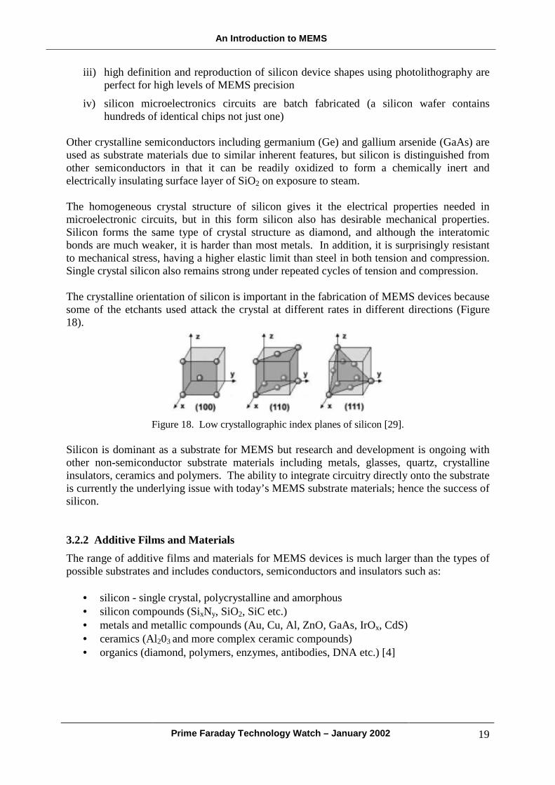
Other crystalline semiconductors including germanium (Ge) and gallium arsenide (GaAs) are used as substrate materials due to similar inherent features, but silicon is distinguished from other semiconductors in that it can be readily oxidized to form a chemically inert and electrically insulating surface layer of SiO2 on exposure to steam. The homogeneous crystal structure of silicon gives it the electrical properties needed in microelectronic circuits, but in this form silicon also has desirable mechanical properties. Silicon forms the same type of crystal structure as diamond, and although the interatomic bonds are much weaker, it is harder than most metals. In addition, it is surprisingly resistant to mechanical stress, having a higher elastic limit than steel in both tension and compression. Single crystal silicon also remains strong under repeated cycles of tension and compression. The crystalline orientation of silicon is important in the fabrication of MEMS devices because some of the etchants used attack the crystal at different rates in different directions (Figure 18).
Figure 18. Low crystallographic index planes of silicon [29].
Silicon is dominant as a substrate for MEMS but research and development is ongoing with other non-semiconductor substrate materials including metals, glasses, quartz, crystalline insulators, ceramics and polymers. The ability to integrate circuitry directly onto the substrate is currently the underlying issue with today’s MEMS substrate materials; hence the success of silicon. 3.2.2 Additive Films and Materials The range of additive films and materials for MEMS devices is much larger than the types of possible substrates and includes conductors, semiconductors and insulators such as:
• silicon - single crystal, polycrystalline and amorphous • silicon compounds (SixNy, SiO2, SiC etc.) • metals and metallic compounds (Au, Cu, Al, ZnO, GaAs, IrOx, CdS) • ceramics (Al203 and more complex ceramic compounds) • organics (diamond, polymers, enzymes, antibodies, DNA etc.) [4]
An Introduction to MEMS
Prime Faraday Technology Watch – January 2002 20
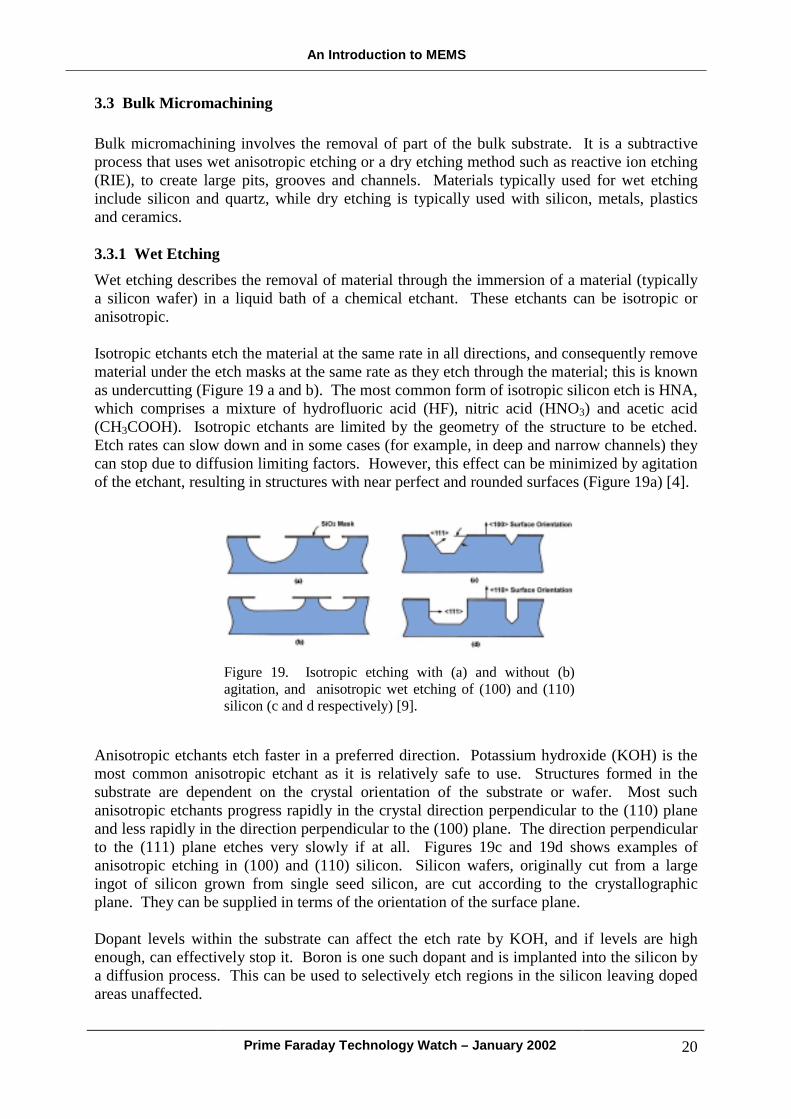
3.3 Bulk Micromachining Bulk micromachining involves the removal of part of the bulk substrate. It is a subtractive process that uses wet anisotropic etching or a dry etching method such as reactive ion etching (RIE), to create large pits, grooves and channels. Materials typically used for wet etching include silicon and quartz, while dry etching is typically used with silicon, metals, plastics and ceramics. 3.3.1 Wet Etching Wet etching describes the removal of material through the immersion of a material (typically a silicon wafer) in a liquid bath of a chemical etchant. These etchants can be isotropic or anisotropic. Isotropic etchants etch the material at the same rate in all directions, and consequently remove material under the etch masks at the same rate as they etch through the material; this is known as undercutting (Figure 19 a and b). The most common form of isotropic silicon etch is HNA, which comprises a mixture of hydrofluoric acid (HF), nitric acid (HNO3) and acetic acid (CH3COOH). Isotropic etchants are limited by the geometry of the structure to be etched. Etch rates can slow down and in some cases (for example, in deep and narrow channels) they can stop due to diffusion limiting factors. However, this effect can be minimized by agitation of the etchant, resulting in structures with near perfect and rounded surfaces (Figure 19a) [4].
Anisotropic etchants etch faster in a preferred direction. Potassium hydroxide (KOH) is the most common anisotropic etchant as it is relatively safe to use. Structures formed in the substrate are dependent on the crystal orientation of the substrate or wafer. Most such anisotropic etchants progress rapidly in the crystal direction perpendicular to the (110) plane and less rapidly in the direction perpendicular to the (100) plane. The direction perpendicular to the (111) plane etches very slowly if at all. Figures 19c and 19d shows examples of anisotropic etching in (100) and (110) silicon. Silicon wafers, originally cut from a large ingot of silicon grown from single seed silicon, are cut according to the crystallographic plane. They can be supplied in terms of the orientation of the surface plane. Dopant levels within the substrate can affect the etch rate by KOH, and if levels are high enough, can effectively stop it. Boron is one such dopant and is implanted into the silicon by a diffusion process. This can be used to selectively etch regions in the silicon leaving doped areas unaffected.
Figure 19. Isotropic etching with (a) and without (b) agitation, and anisotropic wet etching of (100) and (110) silicon (c and d respectively) [9].
An Introduction to MEMS
Prime Faraday Technology Watch – January 2002 21
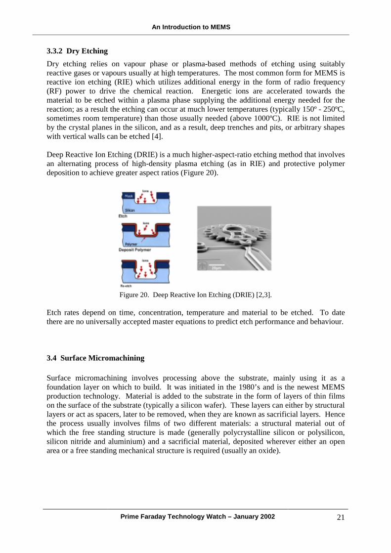
3.3.2 Dry Etching Dry etching relies on vapour phase or plasma-based methods of etching using suitably reactive gases or vapours usually at high temperatures. The most common form for MEMS is reactive ion etching (RIE) which utilizes additional energy in the form of radio frequency (RF) power to drive the chemical reaction. Energetic ions are accelerated towards the material to be etched within a plasma phase supplying the additional energy needed for the reaction; as a result the etching can occur at much lower temperatures (typically 150º - 250ºC, sometimes room temperature) than those usually needed (above 1000ºC). RIE is not limited by the crystal planes in the silicon, and as a result, deep trenches and pits, or arbitrary shapes with vertical walls can be etched [4]. Deep Reactive Ion Etching (DRIE) is a much higher-aspect-ratio etching method that involves an alternating process of high-density plasma etching (as in RIE) and protective polymer deposition to achieve greater aspect ratios (Figure 20).
Figure 20. Deep Reactive Ion Etching (DRIE) [2,3].
Etch rates depend on time, concentration, temperature and material to be etched. To date there are no universally accepted master equations to predict etch performance and behaviour. 3.4 Surface Micromachining Surface micromachining involves processing above the substrate, mainly using it as a foundation layer on which to build. It was initiated in the 1980’s and is the newest MEMS production technology. Material is added to the substrate in the form of layers of thin films on the surface of the substrate (typically a silicon wafer). These layers can either by structural layers or act as spacers, later to be removed, when they are known as sacrificial layers. Hence the process usually involves films of two different materials: a structural material out of which the free standing structure is made (generally polycrystalline silicon or polysilicon, silicon nitride and aluminium) and a sacrificial material, deposited wherever either an open area or a free standing mechanical structure is required (usually an oxide).
An Introduction to MEMS
Prime Faraday Technology Watch – January 2002 22
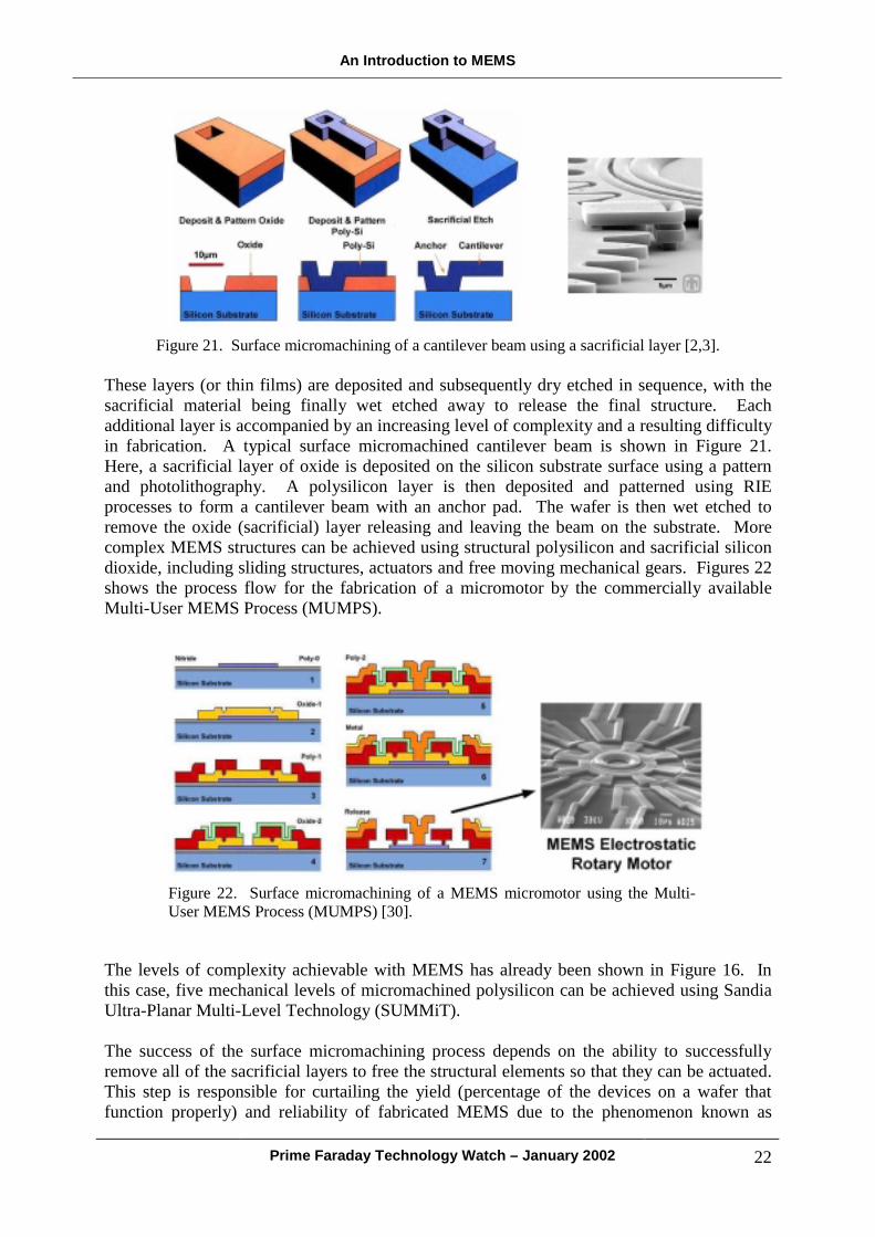
Figure 21. Surface micromachining of a cantilever beam using a sacrificial layer [2,3].
These layers (or thin films) are deposited and subsequently dry etched in sequence, with the sacrificial material being finally wet etched away to release the final structure. Each additional layer is accompanied by an increasing level of complexity and a resulting difficulty in fabrication. A typical surface micromachined cantilever beam is shown in Figure 21. Here, a sacrificial layer of oxide is deposited on the silicon substrate surface using a pattern and photolithography. A polysilicon layer is then deposited and patterned using RIE processes to form a cantilever beam with an anchor pad. The wafer is then wet etched to remove the oxide (sacrificial) layer releasing and leaving the beam on the substrate. More complex MEMS structures can be achieved using structural polysilicon and sacrificial silicon dioxide, including sliding structures, actuators and free moving mechanical gears. Figures 22 shows the process flow for the fabrication of a micromotor by the commercially available Multi-User MEMS Process (MUMPS).
The levels of complexity achievable with MEMS has already been shown in Figure 16. In this case, five mechanical levels of micromachined polysilicon can be achieved using Sandia Ultra-Planar Multi-Level Technology (SUMMiT). The success of the surface micromachining process depends on the ability to successfully remove all of the sacrificial layers to free the structural elements so that they can be actuated. This step is responsible for curtailing the yield (percentage of the devices on a wafer that function properly) and reliability of fabricated MEMS due to the phenomenon known as
Figure 22. Surface micromachining of a MEMS micromotor using the Multi-User MEMS Process (MUMPS) [30].
An Introduction to MEMS
Prime Faraday Technology Watch – January 2002 23
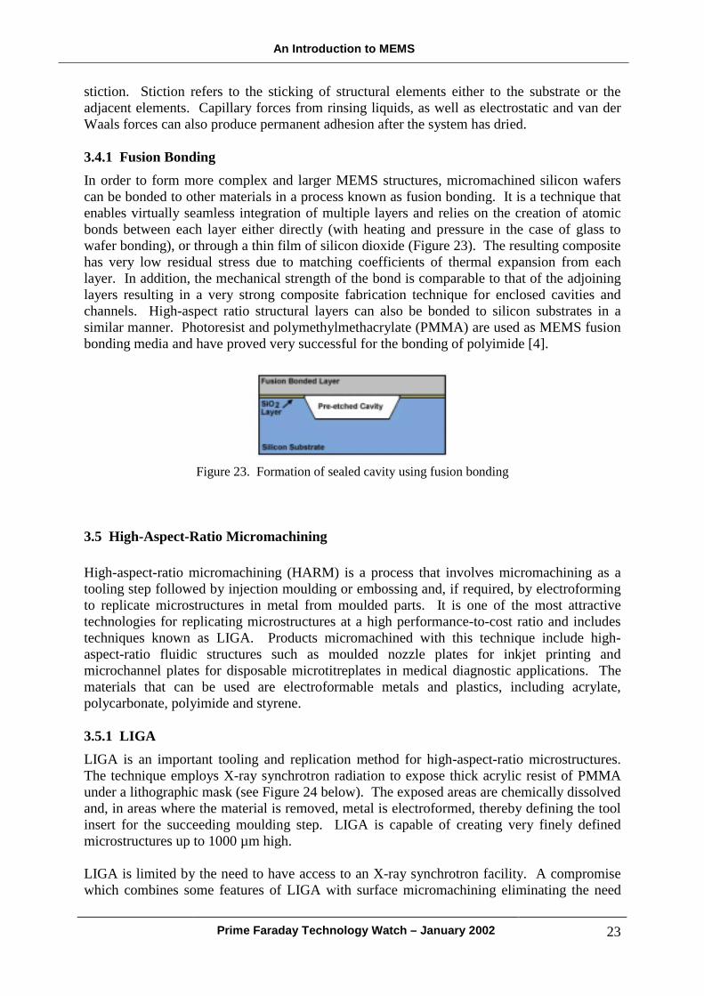
stiction. Stiction refers to the sticking of structural elements either to the substrate or the adjacent elements. Capillary forces from rinsing liquids, as well as electrostatic and van der Waals forces can also produce permanent adhesion after the system has dried. 3.4.1 Fusion Bonding In order to form more complex and larger MEMS structures, micromachined silicon wafers can be bonded to other materials in a process known as fusion bonding. It is a technique that enables virtually seamless integration of multiple layers and relies on the creation of atomic bonds between each layer either directly (with heating and pressure in the case of glass to wafer bonding), or through a thin film of silicon dioxide (Figure 23). The resulting composite has very low residual stress due to matching coefficients of thermal expansion from each layer. In addition, the mechanical strength of the bond is comparable to that of the adjoining layers resulting in a very strong composite fabrication technique for enclosed cavities and channels. High-aspect ratio structural layers can also be bonded to silicon substrates in a similar manner. Photoresist and polymethylmethacrylate (PMMA) are used as MEMS fusion bonding media and have proved very successful for the bonding of polyimide [4].
Figure 23. Formation of sealed cavity using fusion bonding
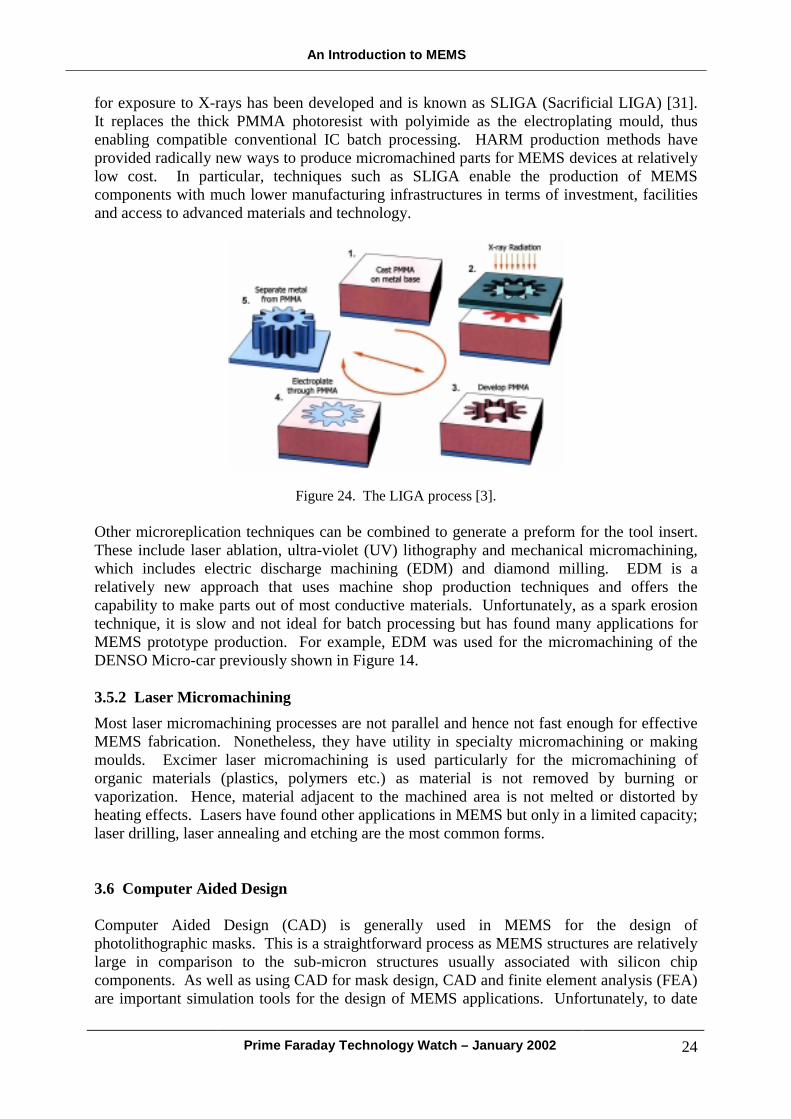
3.5 High-Aspect-Ratio Micromachining High-aspect-ratio micromachining (HARM) is a process that involves micromachining as a tooling step followed by injection moulding or embossing and, if required, by electroforming to replicate microstructures in metal from moulded parts. It is one of the most attractive technologies for replicating microstructures at a high performance-to-cost ratio and includes techniques known as LIGA. Products micromachined with this technique include high-aspect-ratio fluidic structures such as moulded nozzle plates for inkjet printing and microchannel plates for disposable microtitreplates in medical diagnostic applications. The materials that can be used are electroformable metals and plastics, including acrylate, polycarbonate, polyimide and styrene. 3.5.1 LIGA LIGA is an important tooling and replication method for high-aspect-ratio microstructures. The technique employs X-ray synchrotron radiation to expose thick acrylic resist of PMMA under a lithographic mask (see Figure 24 below). The exposed areas are chemically dissolved and, in areas where the material is removed, metal is electroformed, thereby defining the tool insert for the succeeding moulding step. LIGA is capable of creating very finely defined microstructures up to 1000 µm high. LIGA is limited by the need to have access to an X-ray synchrotron facility. A compromise which combines some features of LIGA with surface micromachining eliminating the need
An Introduction to MEMS
Prime Faraday Technology Watch – January 2002 24
for exposure to X-rays has been developed and is known as SLIGA (Sacrificial LIGA) [31]. It replaces the thick PMMA photoresist with polyimide as the electroplating mould, thus enabling compatible conventional IC batch processing. HARM production methods have provided radically new ways to produce micromachined parts for MEMS devices at relatively low cost. In particular, techniques such as SLIGA enable the production of MEMS components with much lower manufacturing infrastructures in terms of investment, facilities and access to advanced materials and technology.
Figure 24. The LIGA process [3]. Other microreplication techniques can be combined to generate a preform for the tool insert. These include laser ablation, ultra-violet (UV) lithography and mechanical micromachining, which includes electric discharge machining (EDM) and diamond milling. EDM is a relatively new approach that uses machine shop production techniques and offers the capability to make parts out of most conductive materials. Unfortunately, as a spark erosion technique, it is slow and not ideal for batch processing but has found many applications for MEMS prototype production. For example, EDM was used for the micromachining of the DENSO Micro-car previously shown in Figure 14. 3.5.2 Laser Micromachining Most laser micromachining processes are not parallel and hence not fast enough for effective MEMS fabrication. Nonetheless, they have utility in specialty micromachining or making moulds. Excimer laser micromachining is used particularly for the micromachining of organic materials (plastics, polymers etc.) as material is not removed by burning or vaporization. Hence, material adjacent to the machined area is not melted or distorted by heating effects. Lasers have found other applications in MEMS but only in a limited capacity; laser drilling, laser annealing and etching are the most common forms. 3.6 Computer Aided Design Computer Aided Design (CAD) is generally used in MEMS for the design of photolithographic masks. This is a straightforward process as MEMS structures are relatively large in comparison to the sub-micron structures usually associated with silicon chip components. As well as using CAD for mask design, CAD and finite element analysis (FEA) are important simulation tools for the design of MEMS applications. Unfortunately, to date
An Introduction to MEMS
Prime Faraday Technology Watch – January 2002 25
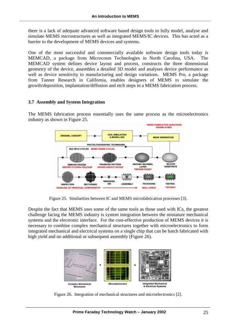
there is a lack of adequate advanced software based design tools to fully model, analyse and simulate MEMS microstructures as well as integrated MEMS/IC devices. This has acted as a barrier to the development of MEMS devices and systems. One of the most successful and commercially available software design tools today is MEMCAD, a package from Microcosm Technologies in North Carolina, USA. The MEMCAD system defines device layout and process, constructs the three dimensional geometry of the device, assembles a detailed 3D model and analyses device performance as well as device sensitivity to manufacturing and design variations. MEMS Pro, a package from Tanner Research in California, enables designers of MEMS to simulate the growth/deposition, implantation/diffusion and etch steps in a MEMS fabrication process. 3.7 Assembly and System Integration The MEMS fabrication process essentially uses the same process as the microelectronics industry as shown in Figure 25.
Figure 25. Similarities between IC and MEMS microfabrication processes [3]. Despite the fact that MEMS uses some of the same tools as those used with ICs, the greatest challenge facing the MEMS industry is system integration between the miniature mechanical systems and the electronic interface. For the cost-effective production of MEMS devices it is necessary to combine complex mechanical structures together with microelectronics to form integrated mechanical and electrical systems on a single chip that can be batch fabricated with high yield and no additional or subsequent assembly (Figure 26).
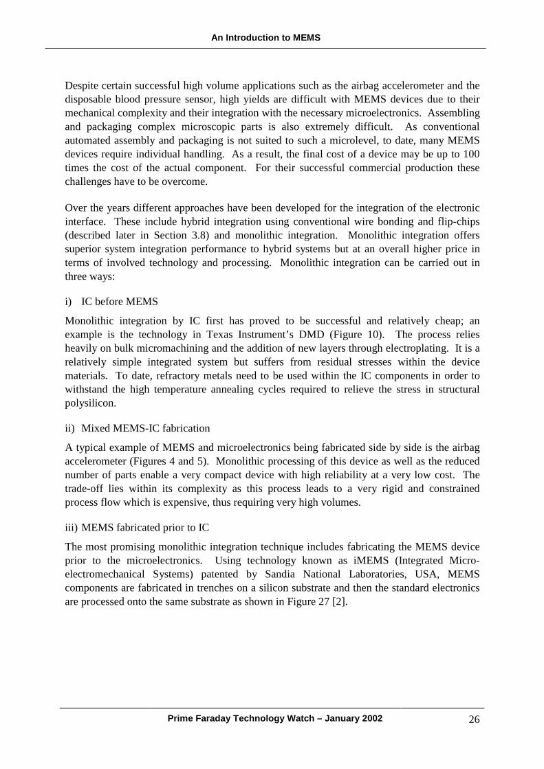
Figure 26. Integration of mechanical structures and microelectronics [2].
An Introduction to MEMS
Prime Faraday Technology Watch – January 2002 26
Despite certain successful high volume applications such as the airbag accelerometer and the disposable blood pressure sensor, high yields are difficult with MEMS devices due to their mechanical complexity and their integration with the necessary microelectronics. Assembling and packaging complex microscopic parts is also extremely difficult. As conventional automated assembly and packaging is not suited to such a microlevel, to date, many MEMS devices require individual handling. As a result, the final cost of a device may be up to 100 times the cost of the actual component. For their successful commercial production these challenges have to be overcome. Over the years different approaches have been developed for the integration of the electronic interface. These include hybrid integration using conventional wire bonding and flip-chips (described later in Section 3.8) and monolithic integration. Monolithic integration offers superior system integration performance to hybrid systems but at an overall higher price in terms of involved technology and processing. Monolithic integration can be carried out in three ways: i) IC before MEMS
Monolithic integration by IC first has proved to be successful and relatively cheap; an example is the technology in Texas Instrument’s DMD (Figure 10). The process relies heavily on bulk micromachining and the addition of new layers through electroplating. It is a relatively simple integrated system but suffers from residual stresses within the device materials. To date, refractory metals need to be used within the IC components in order to withstand the high temperature annealing cycles required to relieve the stress in structural polysilicon. ii) Mixed MEMS-IC fabrication
A typical example of MEMS and microelectronics being fabricated side by side is the airbag accelerometer (Figures 4 and 5). Monolithic processing of this device as well as the reduced number of parts enable a very compact device with high reliability at a very low cost. The trade-off lies within its complexity as this process leads to a very rigid and constrained process flow which is expensive, thus requiring very high volumes. iii) MEMS fabricated prior to IC
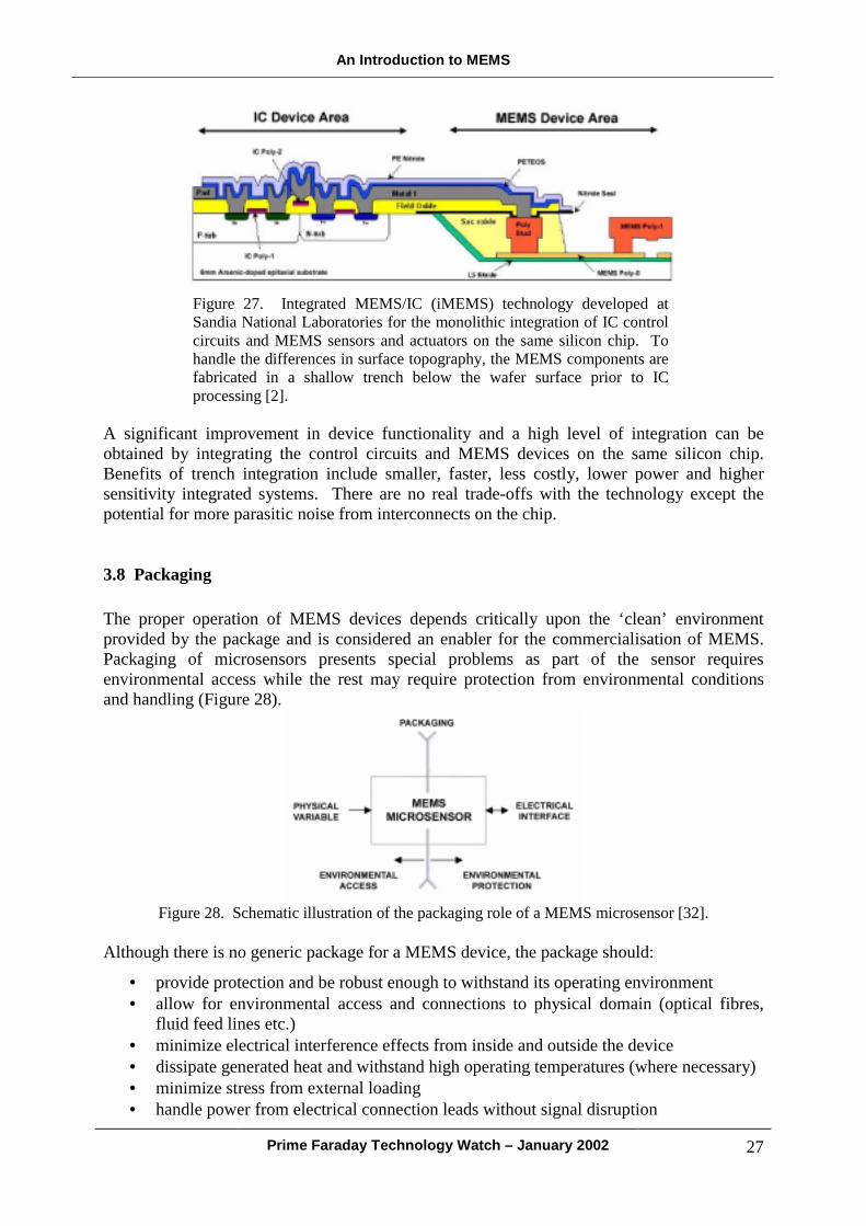
The most promising monolithic integration technique includes fabricating the MEMS device prior to the microelectronics. Using technology known as iMEMS (Integrated Micro-electromechanical Systems) patented by Sandia National Laboratories, USA, MEMS components are fabricated in trenches on a silicon substrate and then the standard electronics are processed onto the same substrate as shown in Figure 27 [2].
An Introduction to MEMS
Prime Faraday Technology Watch – January 2002 27
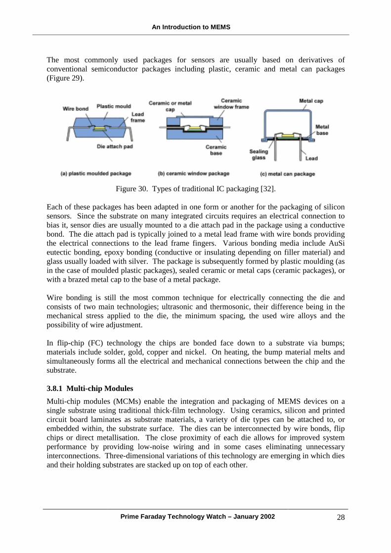
A significant improvement in device functionality and a high level of integration can be obtained by integrating the control circuits and MEMS devices on the same silicon chip. Benefits of trench integration include smaller, faster, less costly, lower power and higher sensitivity integrated systems. There are no real trade-offs with the technology except the potential for more parasitic noise from interconnects on the chip. 3.8 Packaging The proper operation of MEMS devices depends critically upon the ‘clean’ environment provided by the package and is considered an enabler for the commercialisation of MEMS. Packaging of microsensors presents special problems as part of the sensor requires environmental access while the rest may require protection from environmental conditions and handling (Figure 28).
Figure 28. Schematic illustration of the packaging role of a MEMS microsensor [32].
Although there is no generic package for a MEMS device, the package should:
• provide protection and be robust enough to withstand its operating environment • allow for environmental access and connections to physical domain (optical fibres,
fluid feed lines etc.) • minimize electrical interference effects from inside and outside the device • dissipate generated heat and withstand high operating temperatures (where necessary) • minimize stress from external loading • handle power from electrical connection leads without signal disruption
Figure 27. Integrated MEMS/IC (iMEMS) technology developed at Sandia National Laboratories for the monolithic integration of IC control circuits and MEMS sensors and actuators on the same silicon chip. To handle the differences in surface topography, the MEMS components are fabricated in a shallow trench below the wafer surface prior to IC processing [2].
An Introduction to MEMS
Prime Faraday Technology Watch – January 2002 28
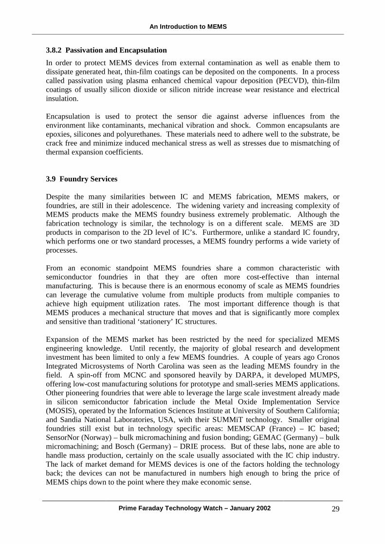
The most commonly used packages for sensors are usually based on derivatives of conventional semiconductor packages including plastic, ceramic and metal can packages (Figure 29).
Figure 30. Types of traditional IC packaging [32].
Each of these packages has been adapted in one form or another for the packaging of silicon sensors. Since the substrate on many integrated circuits requires an electrical connection to bias it, sensor dies are usually mounted to a die attach pad in the package using a conductive bond. The die attach pad is typically joined to a metal lead frame with wire bonds providing the electrical connections to the lead frame fingers. Various bonding media include AuSi eutectic bonding, epoxy bonding (conductive or insulating depending on filler material) and glass usually loaded with silver. The package is subsequently formed by plastic moulding (as in the case of moulded plastic packages), sealed ceramic or metal caps (ceramic packages), or with a brazed metal cap to the base of a metal package. Wire bonding is still the most common technique for electrically connecting the die and consists of two main technologies; ultrasonic and thermosonic, their difference being in the mechanical stress applied to the die, the minimum spacing, the used wire alloys and the possibility of wire adjustment. In flip-chip (FC) technology the chips are bonded face down to a substrate via bumps; materials include solder, gold, copper and nickel. On heating, the bump material melts and simultaneously forms all the electrical and mechanical connections between the chip and the substrate. 3.8.1 Multi-chip Modules Multi-chip modules (MCMs) enable the integration and packaging of MEMS devices on a single substrate using traditional thick-film technology. Using ceramics, silicon and printed circuit board laminates as substrate materials, a variety of die types can be attached to, or embedded within, the substrate surface. The dies can be interconnected by wire bonds, flip chips or direct metallisation. The close proximity of each die allows for improved system performance by providing low-noise wiring and in some cases eliminating unnecessary interconnections. Three-dimensional variations of this technology are emerging in which dies and their holding substrates are stacked up on top of each other.
An Introduction to MEMS
Prime Faraday Technology Watch – January 2002 29
3.8.2 Passivation and Encapsulation In order to protect MEMS devices from external contamination as well as enable them to dissipate generated heat, thin-film coatings can be deposited on the components. In a process called passivation using plasma enhanced chemical vapour deposition (PECVD), thin-film coatings of usually silicon dioxide or silicon nitride increase wear resistance and electrical insulation. Encapsulation is used to protect the sensor die against adverse influences from the environment like contaminants, mechanical vibration and shock. Common encapsulants are epoxies, silicones and polyurethanes. These materials need to adhere well to the substrate, be crack free and minimize induced mechanical stress as well as stresses due to mismatching of thermal expansion coefficients. 3.9 Foundry Services Despite the many similarities between IC and MEMS fabrication, MEMS makers, or foundries, are still in their adolescence. The widening variety and increasing complexity of MEMS products make the MEMS foundry business extremely problematic. Although the fabrication technology is similar, the technology is on a different scale. MEMS are 3D products in comparison to the 2D level of IC’s. Furthermore, unlike a standard IC foundry, which performs one or two standard processes, a MEMS foundry performs a wide variety of processes. From an economic standpoint MEMS foundries share a common characteristic with semiconductor foundries in that they are often more cost-effective than internal manufacturing. This is because there is an enormous economy of scale as MEMS foundries can leverage the cumulative volume from multiple products from multiple companies to achieve high equipment utilization rates. The most important difference though is that MEMS produces a mechanical structure that moves and that is significantly more complex and sensitive than traditional ‘stationery’ IC structures. Expansion of the MEMS market has been restricted by the need for specialized MEMS engineering knowledge. Until recently, the majority of global research and development investment has been limited to only a few MEMS foundries. A couple of years ago Cronos Integrated Microsystems of North Carolina was seen as the leading MEMS foundry in the field. A spin-off from MCNC and sponsored heavily by DARPA, it developed MUMPS, offering low-cost manufacturing solutions for prototype and small-series MEMS applications. Other pioneering foundries that were able to leverage the large scale investment already made in silicon semiconductor fabrication include the Metal Oxide Implementation Service (MOSIS), operated by the Information Sciences Institute at University of Southern California; and Sandia National Laboratories, USA, with their SUMMiT technology. Smaller original foundries still exist but in technology specific areas: MEMSCAP (France) – IC based; SensorNor (Norway) – bulk micromachining and fusion bonding; GEMAC (Germany) – bulk micromachining; and Bosch (Germany) – DRIE process. But of these labs, none are able to handle mass production, certainly on the scale usually associated with the IC chip industry. The lack of market demand for MEMS devices is one of the factors holding the technology back; the devices can not be manufactured in numbers high enough to bring the price of MEMS chips down to the point where they make economic sense.
An Introduction to MEMS
Prime Faraday Technology Watch – January 2002 30
In 1999, the MEMS industry witnessed unprecedented growth and wealth creation as major venture capital and corporate funding took place. Today, it is no longer necessary to build a separate fabrication facility to create a MEMS product or invest hundred of millions of dollars to become a MEMS player. A newly created infrastructure of smaller foundries is now available to support both emerging and proven MEMS-based applications. Although the biggest of these foundries are the risk-taking producers of specialized and niche chips such as Motorola, Sony, Analog Devices and Texas Instruments, there are also many smaller start-up MEMS foundries which offer more specialized services such as packaging, testing, reliability analysis etc. Not only do these foundries offer the obvious manufacturing technology and services to outside customers but they offer the concept of ‘shared learning’ in that lessons learned when the foundry puts into volume production one product can be applied to the subsequent volume production of another product. This can occur even when the products are completely different because there will still be sharing of specific process modules. Today, there are more than 40-50 MEMS makers or foundries worldwide (though none has broken away from the pack as in the case, for example, of Intel with computer chips). 4. MEMS Transducers Microsensors and microactuators are at the very core of a MEMS device or system. A microsensor detects changes in the system’s environment; an ‘intelligent’ part processes the information detected by the sensor and makes a decision in the form of a signal; and a microactuator acts on this signal to create some form of changes in the environment. Microelectronic components make up most of the intelligent part of the device and, as an established technology, will not be discussed here. Sensors and actuators are broadly termed transducers and are essentially devices that convert one form of energy into another. Many of the MEMS sensors and actuators described in this section have been developed within the microelectronics industry and do not all involve any special micromachining techniques; they are based on conventional integrated circuits that, through inherent mechanisms, sense light, temperature etc. However, many of these can be enhanced by the use of MEMS. Basic MEMS mechanisms and structures consist of both in-plane and out-of-plane mechanisms as well as structural members to couple energy between the actuator and sensors as well as with the physical interface of a mechanical system. Mechanisms such as joints, linkages, gears and hinges are very typical. This section concentrates on the phenomena that can be sensed or acted upon with MEMS devices with a brief description of the basic sensing and actuation mechanisms. It is important to note that although these devices are mechanical and have been categorized in terms of their sensing domain (e.g. thermal, chemical, radiation), there are many overlaps, and forms of mechanical transducer can be commonly found as intermediate mechanisms in other devices.
An Introduction to MEMS
Prime Faraday Technology Watch – January 2002 31
4.1 Mechanical Transducers 4.1.1 Mechanical Sensors There is a tremendous variety of direct mechanical sensors that have been or could be micromachined depending on their sensing mechanism (usually piezoresistive, piezoelectric or capacitive) and the parameters sensed (typically strain, force and displacement). i) Piezoresistive sensors
As a result of the piezoresistive effect (defined as the change in resistivity of the material with applied strain), changes in gauge dimension result in proportional changes in resistance in the sensor. The piezoresistive effect in semiconductors is considerably higher than in traditional metals, making silicon an excellent strain sensor. MEMS piezoresistors are readily manufactured using bulk silicon doped with p-type or n-type impurities. ii) Piezoelectric sensors
Piezoelectric sensors utilize the piezoelectric effect in which an applied strain (or force) on a piezoelectric crystal results in a potential difference across the crystal. Similarly, if the crystal is subjected to a potential difference, a displacement, or strain, is produced. The effect can be used to sense mechanical stress (i.e. displacement) and as an actuation mechanism, although displacements are small even for large voltages. Common piezoelectric materials used for MEMS applications include quartz, lead zirconate titanate (PZT), polyvinylidene fluoride (PVDF) and ZnO, PVDF and ZnO being the most common. Silicon is not piezoelectric; hence a thin film of a suitable material must be deposited on the devices. iii) Capacitive sensors
Capacitive (or electrostatic) sensing is one of the most important (and widely used) precision sensing mechanisms and includes one or more fixed conducting plates with one or more moving conducting plates. Capacitive sensing relies on the basic parallel-plate capacitor equation shown below. As capacitance is inversely proportional to the distance between the plates, sensing of very small displacements is extremely accurate.
dAC rεε 0= where: 0ε = permittivity of free space = 8.854x10⁻¹² Fm-1
rε = relative permittivity of material between the plates A = overlapping plate area (m) d = plate separation (m)
iv) Resonant sensors
MEMS resonant sensors consist of micromachined beams or bridges which are driven to vibrate at their resonant frequency. They can be attached to membranes or designed to adhere to a particular substance (as in the case of a biosensor). Movement of the membrane or increased build-up of the binding substance will affect the resonant frequency and can be monitored using implanted piezoresistors. Types of mechanical sensor include:
a) Strain gauge - a strain gauge is a conductor or semiconductor that is fabricated on or bonded directly to the surface to be measured. An example of a polysilicon strain sensor
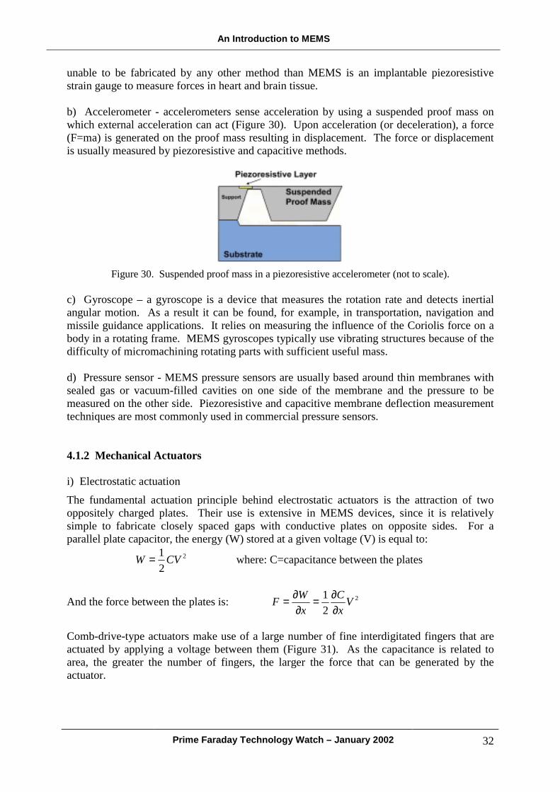
An Introduction to MEMS
Prime Faraday Technology Watch – January 2002 32
unable to be fabricated by any other method than MEMS is an implantable piezoresistive strain gauge to measure forces in heart and brain tissue. b) Accelerometer - accelerometers sense acceleration by using a suspended proof mass on which external acceleration can act (Figure 30). Upon acceleration (or deceleration), a force (F=ma) is generated on the proof mass resulting in displacement. The force or displacement is usually measured by piezoresistive and capacitive methods.
Figure 30. Suspended proof mass in a piezoresistive accelerometer (not to scale).
c) Gyroscope – a gyroscope is a device that measures the rotation rate and detects inertial angular motion. As a result it can be found, for example, in transportation, navigation and missile guidance applications. It relies on measuring the influence of the Coriolis force on a body in a rotating frame. MEMS gyroscopes typically use vibrating structures because of the difficulty of micromachining rotating parts with sufficient useful mass. d) Pressure sensor - MEMS pressure sensors are usually based around thin membranes with sealed gas or vacuum-filled cavities on one side of the membrane and the pressure to be measured on the other side. Piezoresistive and capacitive membrane deflection measurement techniques are most commonly used in commercial pressure sensors. 4.1.2 Mechanical Actuators i) Electrostatic actuation
The fundamental actuation principle behind electrostatic actuators is the attraction of two oppositely charged plates. Their use is extensive in MEMS devices, since it is relatively simple to fabricate closely spaced gaps with conductive plates on opposite sides. For a parallel plate capacitor, the energy (W) stored at a given voltage (V) is equal to:
2
21 CVW = where: C=capacitance between the plates
And the force between the plates is: 2
21 V
xC
xWF
∂∂=
∂∂=
Comb-drive-type actuators make use of a large number of fine interdigitated fingers that are actuated by applying a voltage between them (Figure 31). As the capacitance is related to area, the greater the number of fingers, the larger the force that can be generated by the actuator.
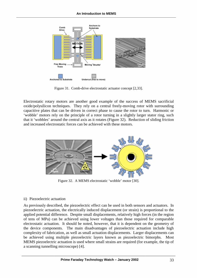
An Introduction to MEMS
Prime Faraday Technology Watch – January 2002 33
Figure 31. Comb-drive electrostatic actuator concept [2,33].
Electrostatic rotary motors are another good example of the success of MEMS sacrificial oxide/polysilicon techniques. They rely on a central freely-moving rotor with surrounding capacitive plates that can be driven in correct phase to cause the rotor to turn. Harmonic or ‘wobble’ motors rely on the principle of a rotor turning in a slightly larger stator ring, such that it ‘wobbles’ around the central axis as it rotates (Figure 32). Reduction of sliding friction and increased electrostatic forces can be achieved with these motors.
Figure 32. A MEMS electrostatic ‘wobble’ motor [30].
ii) Piezoelectric actuation
As previously described, the piezoelectric effect can be used in both sensors and actuators. In piezoelectric actuation, the electrically induced displacement (or strain) is proportional to the applied potential difference. Despite small displacements, relatively high forces (in the region of tens of MPa) can be achieved using lower voltages than those required for comparable electrostatic actuation. It should be noted, however, that it is dependent on the geometry of the device components. The main disadvantages of piezoelectric actuation include high complexity of fabrication, as well as small actuation displacements. Larger displacements can be achieved using multiple piezoelectric layers known as piezoelectric bimorphs. Most MEMS piezoelectric actuation is used where small strains are required (for example, the tip of a scanning tunnelling microscope) [4].
An Introduction to MEMS
Prime Faraday Technology Watch – January 2002 34
4.2 Radiation Transducers 4.2.1 Radiation Sensors Radiation sensors cover ionising radiation as well as visible light, infra-red (IR) and ultra-violet (UV) radiation. Current ionising radiation sensors for high-energy particles and X-rays include Geiger-Müller (GM) tubes and scintillators and although they have not been realized using MEMS, their miniaturization is potentially feasible. Sensors for visible, IR and UV radiation are generally categorized as either direct or indirect. Direct optical sensors detect photons and result in an electronic signal. Indirect sensors convert the optical signals into an intermediate energy form (e.g. thermal or chemical), which is then measured electrically. There are a wide variety of both direct and indirect sensors and only the most common will be described here. i) Photodiodes
A photodiode is a semiconductor device for measuring light intensity based on the photoconductive effect (increase in conductivity of a semiconductor on exposure to light). Photodiodes are junction-based photoelectrodes which have a p-n junction. When visible or near infra-red light falls on the device, additional charge carriers are generated resulting in increased current flow. ii) Charge-coupled devices
Charge-coupled devices (CCDs) are one of the most common photodetectors used in handheld video recorders and many other consumer applications. They consist of a metal gate (electrode) above a dielectric and a semiconductor substrate. This forms a metal oxide semiconductor (MOS) capacitor, the charge on which arises from photogenerated carriers. CCDs can be linear or made up of arrays of metal-insulator-semiconductor sensors arranged so that photo-generated charge can be stored and transferred between elements by an appropriate variation of control voltages applied to surface electrodes (memory/signal processing approach). iii) Pyroelectric sensors
Pyroelectric detectors are an example of indirect optical sensors and are essentially capacitors whose charge can be altered by illumination or temperature changes. By converting incident light into heat, which is then measured, pyroelectric sensors have a wide range of applications in surveillance, military, security consumer markets etc. e.g. human motion detectors. Pyroelectric sensors use piezoelectric and ferroelectric materials (varying dielectric constant with applied voltage). ZnO is the most common in MEMS devices. 4.2.2 Radiation (Optical) Actuators The two most common forms of optical actuation include light emitting diodes and light modulators such as liquid crystal displays and reflective micromechanical light modulators (technology used in Texas Instrument’s DMD projection system). Optical devices can either be active or passive; active devices include laser emitting diodes, photodiodes and optical switches. Passive devices include couplers, mirrors, wavelength division multiplexers, polarisers etc. Their application is important in both optical MEMS
An Introduction to MEMS
Prime Faraday Technology Watch – January 2002 35
devices and integrated optics to enable the control and analysis of optical acquired data. A brief selection of optical MEMS components includes:
• optical waveguides to route optical energy from one region to another. MEMS techniques are commonly employed to enable waveguide-to-photodiode coupling.
• fibre-optic couplers incorporate micromachined grooves and channels as mechanical
couplings for fibre-optic components. Anisotropic wet etching, DRIE and HARM methods are typically used.
• micromirrors with flawless surfaces can be achieved using anisotropic etching to yield
perfect crystal plane surfaces. 4.3 Thermal Transducers 4.3.1 Thermal Sensors i) Thermo-mechanical sensors
Thermo-mechanical sensing (and actuation) utilize the fact that all materials have a coefficient of thermal expansion. Consequently, if two different materials are sandwiched together and undergo a temperature change, movement in the sandwich assembly would occur. This is the basis for the common bimetallic (or thermal bimorph) sensing and actuation. ii) Thermoresistive sensors
Thermoresistive sensors rely on the fact that the resistivity, ρ , of most materials changes with temperature and is shown by the equation )1( 2bTaTR =+=ρ where R is the resistivity of the material at a reference temperature, T (ºC), and a and b are constants specific to the material being used. The rate of change of resistance with temperature is known as the temperature coefficient of resistance. Most common materials exhibit an increase in resistance with temperature (e.g. platinum is particularly linear with temperature). Certain materials – for example, carbon, some ceramics and most semiconductors used in thermoresistors or ‘thermistors’ – exhibit a decrease in resistance with increasing temperature. They are not as linear as platinum, but often cheaper to fabricate and easier to integrate with circuitry in MEMS devices. iii) Thermocouples
The thermocouple is probably the most common temperature transducer. It consists of a junction between two different materials and measures the temperature-dependent voltage that arises across the junction. Semiconductor materials often exhibit a better thermoelectric effect than metals. Thermocouples have been used in a wide variety of MEMS sensors in an array arrangement referred to as a thermopile. 4.3.2 Thermal Actuators Thermal actuation in MEMS is usually as a direct result of incorporating tiny heaters, or resistors. These resistors can be controlled to locally heat specific areas or layers as in the case of a bilayer actuator. As already detailed, basic thermal actuation utilizes the difference

An Introduction to MEMS
Prime Faraday Technology Watch – January 2002 36
in thermal coefficients for expansion of two bonded materials and is referred to as thermal bimorph actuation. A typical thermal bimorph actuator is shown in Figure 33.
Figure 33. Example of a MEMS thermal bimorph actuator [34].
This can be applied to a volume of fluid (liquid or gases) in sealed cavities with a thin membrane as a wall. By incorporating a heater the liquid can be heated causing it to expand and deform the membrane outwards. Large forces can be achieved using thermally actuated devices but power consumption can be high and it can take time for material to cool to its original activation state. i) Shape memory alloy actuation Shape memory alloys (SMAs) exhibit considerable changes in their length (contraction) when heated. These include titanium/nickel alloys, of which some, once mechanically deformed, would return to their original undeformed state when heated. Being conductive they can be heated simply by passing a current through them. 4.4 Magnetic Transducers 4.4.1 Magnetic Sensors Most MEMS magnetic sensors are based on the Hall effect. They rely on the production of an electric field across a material through which an electric current is flowing and where a magnetic field is acting. The force applied to the charge carriers by the electric field exactly balances a force from the magnetic field called the Lorentz force. Other ways to sense magnetic fields use optical sensors that rely on the magneto-optical effect or materials that exhibit magnetic anisotropy (shape, stress and crystalline anisotropy are particularly common in MEMS magnetic applications). Magnetic coils are not common in MEMS as they tend to be 2D, which is not useful for many applications. The most sensitive magnetic sensors include superconducting quantum interference devices (SQUIDS). The devices can detect diminutive magnetic fluxes produced by the electric currents in heart and brain tissue. Advances in superconducting thin films as well as MEMS techniques have accelerated growth with these devices. Most of today’s magnetic sensors are silicon based, not only because of the ease of fabrication and their ability to be readily integrated with circuitry, but also because their high volume demand necessitates lower cost.
An Introduction to MEMS
Prime Faraday Technology Watch – January 2002 37
4.4.2 Magnetic Actuators Magnetic actuation is based on the fact that a current-carrying conductor generates a magnetic field. If this conductor is a wire (or coil) and interacts with another external magnetic field (e.g. from a similar conductor or coil) a mechanical force is produced. Despite the success of magnetic actuation on a macroscale, such as motors or solenoids, MEMS magnetic devices are still relatively unestablished. This is due to the fact that 3D coils are very difficult to fabricate by MEMS. A notable exception is the magnetic read/write heads for computer disk drives. This device can be classified as both a sensor and actuator in that it reads from and writes to magnetic media. Choice of magnetic material is limited to those that can be easily micromachined and do not suffer from high power consumption and heat dissipation. Thin film permanent magnets can be fabricated using MEMS; LIGA is particularly common for polymers such as polyimide which can be loaded with a magnetic powder and electroplated. Although attempts have been made to fabricate MEMS magnetic actuators with wire-bonded coils, often in MEMS devices, magnetic actuators compete with electrostatic devices which are stronger for the same volume. i) Magnetostrictive Actuators These rely on the magnetostrictive effect, which is the change of shape or size of a ferromagnetic material induced by a magnetic field, for example, the contraction of a nickel rod under a longitudinal magnetic field. 4.5 Chemical and Biological Transducers 4.5.1 Chemical and Biological Sensors Chemical and biological sensors encompass a large and wide variety of devices that interact with solids, gases and liquids of all types and are therefore extremely diverse and interdisciplinary. They are different from previously described sensors in that they must directly interact with a chemical medium to connect the chemical and electrical domains. Hence they require ‘openings’ within their packaging to enable this interaction (like pressure sensors). Most chemical and biological sensors do not require extremely sophisticated micromachining but can require considerable interdisciplinary knowledge and sophistication for their actual use. Chemical sensors must be very highly selective in order to make such identifications among compounds without falsely responding to potential interfering species. Chemical sensors can be categorized in many ways including passive chemical sensors, work function based systems and electrochemical transducers. Passive chemical sensors include:
• Chemiresistors measure the resistance of a chemically sensitive layer between two electrical contacts. Sensitivity can be increased using more micromachined electrodes.
An Introduction to MEMS
Prime Faraday Technology Watch – January 2002 38
• Chemicapacitors are similar to chemiresistors but the capacitance of the sensitive layer is measured. Chemicapacitors have found application in sensing humidity.
• Chemomechanical sensors rely on direct chemical-to-mechanical transduction (for
example, the expansion of a thin-film polymer in the presence of a substance being analysed).
• Calorimetric sensors measure heat generated by chemical reactions.
i) Work function based sensors
This class of sensors, including the ion sensitive field effect transistor (ISFET) and the metal oxide semiconductor field effect transistor (MOSFET), utilizes metal-insulator-semiconductor junctions and the fact that the work function of the material at the interfaces can be chemically modulated. The ISFET was developed as a direct result of the fact that metal-oxide-semiconductor transistors were so sensitive to surface contaminants during their manufacture. As a large proportion of chemical sensors are based on the ISFET, a more detailed description of their operation is outlined. ISFETs sense the concentration or activity level of a particular ion in solution. The ISFET is a derivative of a common electronic component called a MOSFET. This consists of a silicon semiconductor substrate (doped with impurities to make it p-type) and two electrical contacts (source and drain) doped with impurities so that negatively charged electrons are the main carriers in these small n-type silicon regions. A small distance separates source from drain (Figure 34). Overlaying the substrate between the source and drain is a silicon dioxide insulator which itself is overlaid with a metal electrode called a gate. When a potential is applied to the gate of the MOSFET, the induced electrical field changes the freedom with which the current flows between the source and the drain. In the case of an ISFET however, there is no gate electrode and the insulator is in direct contact with an electrolyte solution to be measured. With the ISFET, electric current flows from the source to the drain via a channel. As in the MOSFET the channel resistance depends on the electric field perpendicular to the direction of the current. Also it depends on the potential difference over the gate oxide. Therefore the source-drain current is influenced by the interface potential at the oxide/aqueous junction. When SiO2 is used as the insulator, the chemical nature of the interface oxide is reflected in the measured source-drain current. With the selection of other appropriate insulator material, such as silicon nitride or aluminium oxide, hydrogen ions will reside at the surface of the insulator in proportion to the pH. Their positive charge produces an electric field that modulates the current between the source and drain. In order to quantify this effect, the control voltage is measured that must be applied (via a reference electrode) to maintain the drain-source current at a constant value. The chemical sensitivity of the ISFET is completely controlled by the properties of the electrolyte/insulator interface. One significant problem in the design and fabrication of ISFETs is ensuring that the selective membrane adheres to the device. If the integrity of the membrane is compromised, then the device is useless.
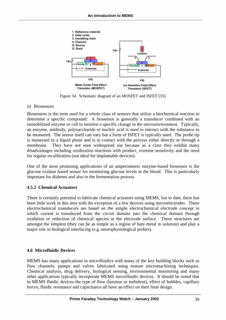
An Introduction to MEMS
Prime Faraday Technology Watch – January 2002 39
Figure 34. Schematic diagram of an MOSFET and ISFET [35].
ii) Biosensors Biosensors is the term used for a whole class of sensors that utilize a biochemical reaction to determine a specific compound. A biosensor is generally a transducer combined with an immobilized enzyme or cell to monitor a specific change in the microenvironment. Typically, an enzyme, antibody, polysaccharide or nucleic acid is used to interact with the substance to be measured. The sensor itself can vary but a form of ISFET is typically used. The probe tip is immersed in a liquid phase and is in contact with the process either directly or through a membrane. They have not seen widespread use because as a class they exhibit many disadvantages including oxidization reactions with product, extreme sensitivity and the need for regular recalibration (not ideal for implantable devices). One of the most promising applications of an amperometric enzyme-based biosensor is the glucose oxidase based sensor for monitoring glucose levels in the blood. This is particularly important for diabetes and also in the fermentation process. 4.5.2 Chemical Actuators There is certainly potential to fabricate chemical actuators using MEMS, but to date, there has been little work in this area with the exception of a few devices using microelectrodes. These electrochemical transducers are based on the simple electrochemical electrode concept in which current is transduced from the circuit domain into the chemical domain through oxidation or reduction of chemical species at the electrode surface. These structures are amongst the simplest (they can be as simple as a region of bare metal in solution) and play a major role in biological interfacing (e.g. neurophysiological probes). 4.6 Microfluidic Devices MEMS has many applications in microfluidics with many of the key building blocks such as flow channels, pumps and valves fabricated using mature micromachining techniques. Chemical analysis, drug delivery, biological sensing, environmental monitoring and many other applications typically incorporate MEMS microfluidic devices. It should be noted that in MEMS fluidic devices the type of flow (laminar or turbulent), effect of bubbles, capillary forces, fluidic resistance and capacitance all have an effect on their final design.
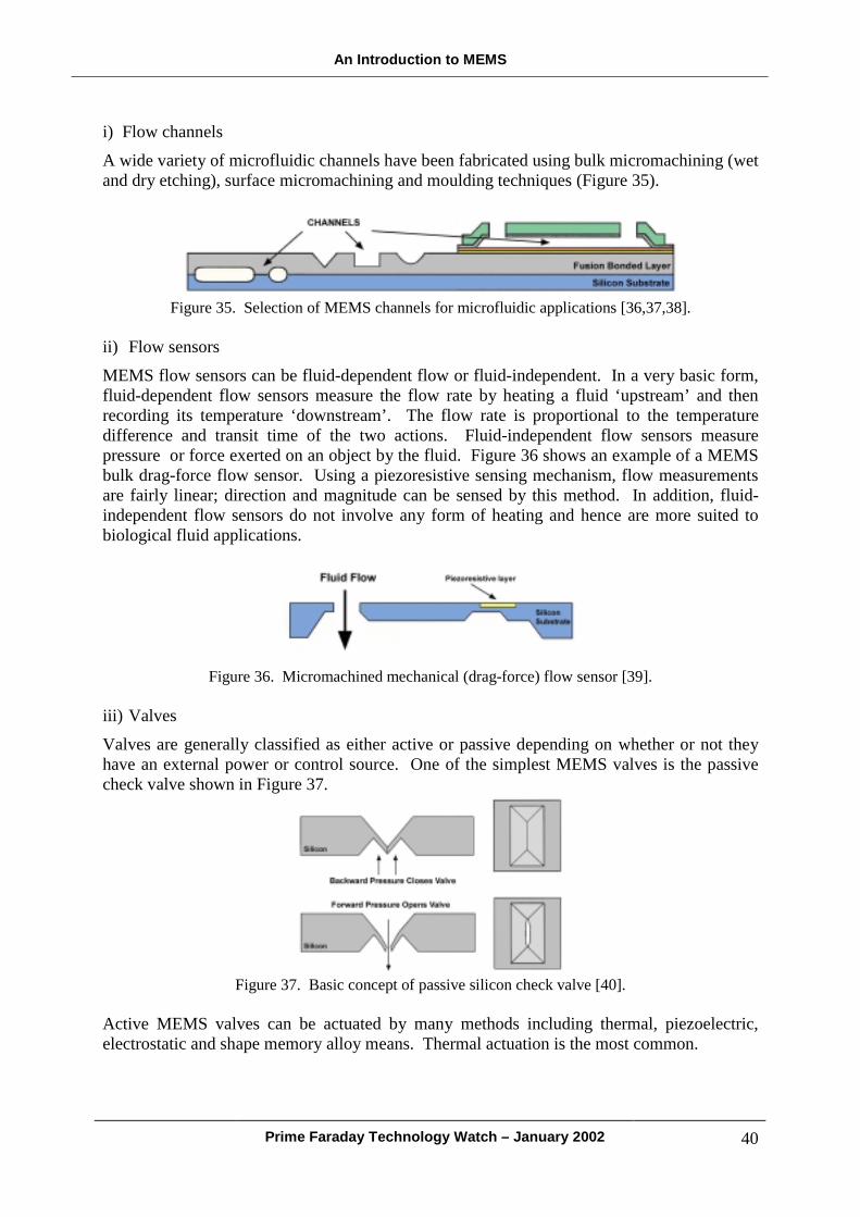
An Introduction to MEMS
Prime Faraday Technology Watch – January 2002 40
i) Flow channels
A wide variety of microfluidic channels have been fabricated using bulk micromachining (wet and dry etching), surface micromachining and moulding techniques (Figure 35).
Figure 35. Selection of MEMS channels for microfluidic applications [36,37,38].
ii) Flow sensors
MEMS flow sensors can be fluid-dependent flow or fluid-independent. In a very basic form, fluid-dependent flow sensors measure the flow rate by heating a fluid ‘upstream’ and then recording its temperature ‘downstream’. The flow rate is proportional to the temperature difference and transit time of the two actions. Fluid-independent flow sensors measure pressure or force exerted on an object by the fluid. Figure 36 shows an example of a MEMS bulk drag-force flow sensor. Using a piezoresistive sensing mechanism, flow measurements are fairly linear; direction and magnitude can be sensed by this method. In addition, fluid-independent flow sensors do not involve any form of heating and hence are more suited to biological fluid applications.
Figure 36. Micromachined mechanical (drag-force) flow sensor [39].
iii) Valves
Valves are generally classified as either active or passive depending on whether or not they have an external power or control source. One of the simplest MEMS valves is the passive check valve shown in Figure 37.
Figure 37. Basic concept of passive silicon check valve [40].
Active MEMS valves can be actuated by many methods including thermal, piezoelectric, electrostatic and shape memory alloy means. Thermal actuation is the most common.
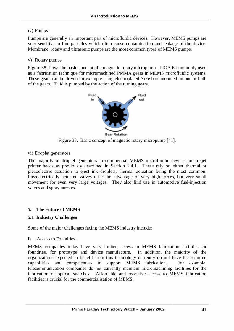
An Introduction to MEMS
Prime Faraday Technology Watch – January 2002 41
iv) Pumps
Pumps are generally an important part of microfluidic devices. However, MEMS pumps are very sensitive to fine particles which often cause contamination and leakage of the device. Membrane, rotary and ultrasonic pumps are the most common types of MEMS pumps. v) Rotary pumps
Figure 38 shows the basic concept of a magnetic rotary micropump. LIGA is commonly used as a fabrication technique for micromachined PMMA gears in MEMS microfluidic systems. These gears can be driven for example using electroplated NiFe bars mounted on one or both of the gears. Fluid is pumped by the action of the turning gears.
Figure 38. Basic concept of magnetic rotary micropump [41].
vi) Droplet generators The majority of droplet generators in commercial MEMS microfluidic devices are inkjet printer heads as previously described in Section 2.4.1. These rely on either thermal or piezoelectric actuation to eject ink droplets, thermal actuation being the most common. Piezoelectrically actuated valves offer the advantage of very high forces, but very small movement for even very large voltages. They also find use in automotive fuel-injection valves and spray nozzles. 5. The Future of MEMS 5.1 Industry Challenges Some of the major challenges facing the MEMS industry include: i) Access to Foundries.
MEMS companies today have very limited access to MEMS fabrication facilities, or foundries, for prototype and device manufacture. In addition, the majority of the organizations expected to benefit from this technology currently do not have the required capabilities and competencies to support MEMS fabrication. For example, telecommunication companies do not currently maintain micromachining facilities for the fabrication of optical switches. Affordable and receptive access to MEMS fabrication facilities is crucial for the commercialisation of MEMS.
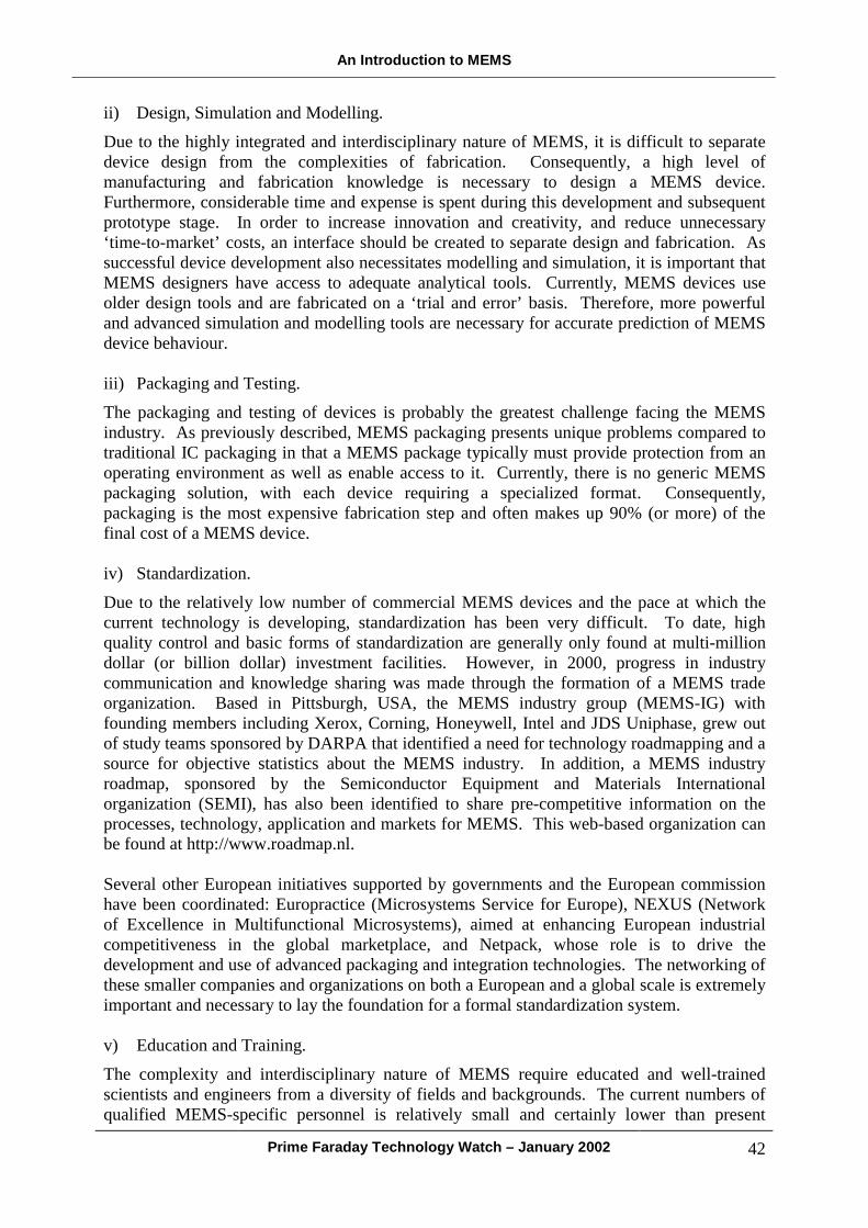
An Introduction to MEMS
Prime Faraday Technology Watch – January 2002 42
ii) Design, Simulation and Modelling.
Due to the highly integrated and interdisciplinary nature of MEMS, it is difficult to separate device design from the complexities of fabrication. Consequently, a high level of manufacturing and fabrication knowledge is necessary to design a MEMS device. Furthermore, considerable time and expense is spent during this development and subsequent prototype stage. In order to increase innovation and creativity, and reduce unnecessary ‘time-to-market’ costs, an interface should be created to separate design and fabrication. As successful device development also necessitates modelling and simulation, it is important that MEMS designers have access to adequate analytical tools. Currently, MEMS devices use older design tools and are fabricated on a ‘trial and error’ basis. Therefore, more powerful and advanced simulation and modelling tools are necessary for accurate prediction of MEMS device behaviour. iii) Packaging and Testing.
The packaging and testing of devices is probably the greatest challenge facing the MEMS industry. As previously described, MEMS packaging presents unique problems compared to traditional IC packaging in that a MEMS package typically must provide protection from an operating environment as well as enable access to it. Currently, there is no generic MEMS packaging solution, with each device requiring a specialized format. Consequently, packaging is the most expensive fabrication step and often makes up 90% (or more) of the final cost of a MEMS device. iv) Standardization.
Due to the relatively low number of commercial MEMS devices and the pace at which the current technology is developing, standardization has been very difficult. To date, high quality control and basic forms of standardization are generally only found at multi-million dollar (or billion dollar) investment facilities. However, in 2000, progress in industry communication and knowledge sharing was made through the formation of a MEMS trade organization. Based in Pittsburgh, USA, the MEMS industry group (MEMS-IG) with founding members including Xerox, Corning, Honeywell, Intel and JDS Uniphase, grew out of study teams sponsored by DARPA that identified a need for technology roadmapping and a source for objective statistics about the MEMS industry. In addition, a MEMS industry roadmap, sponsored by the Semiconductor Equipment and Materials International organization (SEMI), has also been identified to share pre-competitive information on the processes, technology, application and markets for MEMS. This web-based organization can be found at http://www.roadmap.nl. Several other European initiatives supported by governments and the European commission have been coordinated: Europractice (Microsystems Service for Europe), NEXUS (Network of Excellence in Multifunctional Microsystems), aimed at enhancing European industrial competitiveness in the global marketplace, and Netpack, whose role is to drive the development and use of advanced packaging and integration technologies. The networking of these smaller companies and organizations on both a European and a global scale is extremely important and necessary to lay the foundation for a formal standardization system. v) Education and Training.
The complexity and interdisciplinary nature of MEMS require educated and well-trained scientists and engineers from a diversity of fields and backgrounds. The current numbers of qualified MEMS-specific personnel is relatively small and certainly lower than present
An Introduction to MEMS
Prime Faraday Technology Watch – January 2002 43
industry demand. Education at graduate level is usually necessary and although the number of universities offering MEMS-based degrees is increasing, gaining knowledge is an expensive and time-consuming process. Therefore, in order to match the projected need for these MEMS scientists and engineers, an efficient and lower cost education methodology is necessary. One approach, for example, is industry-led (or driven) academic research centres offering technology-specific programmes with commercial integration, training and technology transfer. 5.2 The Way Ahead The market for MEMS devices is still being developed but does not have the explosive growth of, for example, the IC industry in the 1970s. Comparison will always be made between the two, but this is not realistic as there is no ‘dominant technology’ in MEMS analogous to metal oxide semiconductor circuitry, which accelerated the exponential growth of the digital electronics industry. Most of the research today is focused on surface micromachining, but in industry the majority of shipped devices are still manufactured using much older bulk methods. Although some surface micromachined devices are being produced in volume, it will take a few more years for this approach to make a large impact; devices using both surface and bulk continue to be marketed. Despite MEMS being an enabling technology for the development and production of many new industrial and consumer products, MEMS is also a disruptive technology in that it differs significantly from existing technology, requiring a completely different set of capabilities and competencies to implement it. MEMS involves major scaling, packaging and testing issues, and, as a disruptive technology, faces challenges associated with developing manufacturing processes that no longer fit established methods. For the true commercialisation of MEMS, foundries must overcome the critical technological bottlenecks, the economic feasibility of integrating MEMS-based components, as well as the market uncertainty for such devices and applications. Cost reduction is critical and will ultimately result from better availability of infrastructure, more reliable manufacturing processes and technical information as well as new standards on interfacing.
An Introduction to MEMS
Prime Faraday Technology Watch – January 2002 44
References General References Angell, J.B., Terry, S.C., Barth, P.W., Silicon Micromechanical Devices, Scientific American, April 1983, Vol. 248, pp. 44-55. Banks, D., Introduction to Microengineering, http://www.dbanks.demon.co.uk/ueng/ what.html De Los Santos, H.J., Introduction to Microelectromechanical (MEM) Microwave Systems, Artech House Microwave Library, Artech House, Boston, MA, 1999. Feynman, R., There’s Plenty of Room at the Bottom, Journal of Microelectromechanical Systems, March 1992, Vol.1, No.1, pp. 60-66. Kovacs, G.T.A., Micromachined Transducers Sourcebook, McGraw-Hill, New York, NY, 1998. Madou, M., Fundamentals of Microfabrication, CRC Press, Inc., Boca Raton, FL, 1997. Muller, R.S., Howe, R.T., Senturia, S.D., Smith, R.L., and White, R.M. [Eds.], Microsensors, IEEE Press, New York, NY, 1991. Trimmer, W.S., Micromechanics and MEMS: Classic and Seminal Papers to 1990, IEEE Press, New York, NY, 1997. Specific References 1. Berkeley Sensor and Actuator Center, http://bsac.eecs.berkeley.edu 2. Sandia National Laboratories, SUMMiT * Technologies, http://www.mems.sandia.gov 3. Defense Advanced Research Projects Agency (DARPA), http://www.darpa.mil/MTO/ 4. Kovacs, G.T.A., Micromachined Transducers Sourcebook, McGraw-Hill, New York, NY,
1998. 5. Lion, K.S., Transducers: Problems and Prospects, IEEE Transactions on Industrial
Electronics and Control Instrumentation, Vol. IECI-16, No.1, July 1969, pp. 2-5. 6. White, R.M., A Sensor Classification Scheme, IEEE Transactions on Ultrasonics,
Ferroelectrics and Frequency Control, Vol UFFC-34, No.2, March 1987, pp. 124-126. 7. Ristic, Lj. [Ed.], Sensor Technology and Devices, Artech House, London, 1994. 8. University of Stanford, http://www.stanford.edu/group/SML/ee321/ho/MEMS-01-
intro.pdf 9. Petersen, K.E., Silicon as a Mechanical Material, Proceedings of the IEEE, May 1982,
Vol. 70, No. 5, pp.420-457. 10. Memscap, http://www.memscap.com 11. Walsh, S., Linton, J., Grace, R., Marshall, Knutti, S., MEMS and MOEMS Technology
and Applications, edited by Rai Choudry, P., SPIE – The International Society for Optical Engineering, Bellingham, WA, Ch. 8, 2000.
12. Analog Devices Inc., http://www.analog.com 13. Lucas Novasensor, http://www.novasensor.com
An Introduction to MEMS
Prime Faraday Technology Watch – January 2002 45
14. Motorola, Sensor Products Divison, http://www.motorola.com 15. Perkin-Elmer Applied Biosystems, http://www.perkin-elmer.com,
http://www.appliedbiosystems.com 16. Hewlett-Packard, http://www.hp.com 17. Texas Instruments Inc., http://www.ti.com 18. STEAG microParts GmbH, http://microparts.de 19. Merlin Diagnostika GmbH, http://www.merlin-diagnostika.de 20. Bell Labs, http://www.bell-labs.com 21. Lucent Technologies, http://www.lucent.com 22. Agilent Technologies, http://www.agilent.com 23. NEXUS (The Network of Excellence in Multifunctional Microsystems) Task Force,
Market Analysis for Microsystems: 1996-2002, 1998, http://www.nexus-emsto.com 24. System Planning Corporation (SPC), MicroElectromechanical Systems (MEMS): An
SPC Study, 1994. 25. Battelle Institute, Micromechanics, Battelle Institute, Frankfurt am Main, 1992 26. Roger Grace Associates, http://www.rgrace.com 27. Denso Corporation, http://www.denso-int.com 28. Jaeger, R.C., Introduction to Microelectronics Fabrication, Vol. V, Modular Series on
Solid State Devices, (Neudeck, G.W. and Pierret, R.F., Eds.), Addison-Wesley, Reading, MA, 1988.
29. Sze, S.M., Semiconductor Sensors, John Wiley and Sons, Sommerset, NJ, 1994. 30. MCNC, http://www.mcnc.org 31. Bryzek, J., Peterson, K., and McCulley, W., Micromachines on the March, IEEE
Spectrum, 1994, pp. 20-31. 32. Elwenspoek, M., Wiegerink, R.J., Mechanical Microsensors, Springer, Berlin, Germany,
2001. 33. Judy, M.W., and Howe, R.T., Polysilicon Hollow Beam Lateral Resonators, Proceedings
of the IEEE Microelectromechanical Systems Conference, Fort Lauderdale, FL, Feb. 7-10, 1993, pp. 265-271.
34. Riethmuller, W. and Benecke, W., ‘Thermally Excited Silicon Microactuators, IEEE Transactions on Electron Devices, vol.35, no.6, June 1988, pp.758-763.
35. University of Warsaw, Warsaw, Poland 36. Sobek, D., Senturia, S.D., and Gray, M.L., Microfabricated Fused Silica Flow Chambers
for Flow Cytometry, Proceedings of the Solid-State Sensor and Actuator Workshop, Hilton Head Island, SC, June 13-16, 1994, pp. 260-263.
37. Tjerkstra, R. W., de Boer, M., Berenschot, E., Gardeniers, J.G.E., van der Berg, A., and Elwenspoek, M., Etching Technology for Microchannels, Proceedings of the 10th Annual Workshop of Micro Electro Mechanical Systems (MEMS ’97), Nagoya, Japan, Jan. 26-30, 1997, pp. 396-398.
An Introduction to MEMS
Prime Faraday Technology Watch – January 2002 46
38. Man, P.F., Jones, D.K. and Mastrangelo, C.H., Microfluidic Plastic Capillaries on Silicon Substrates: A New Inexpensive Technology for Bioanalysis Chips, Proceedings of the 10th Annual Workshop of Micro Electro Mechanical Systems (MEMS ’97), Nagoya, Japan, Jan. 26-30, 1997, pp.311-316.
39. Gass, V., van der Schoot, B.H., Jeanneret, S., and de Rooji, N.F., Integrated Flow-Regulated Silicon Micropump, Proceedings of Transducers ’93, the 7th International Conference on Solid-State Sensors and Actuators, Yokohama, Japan, June 7-10, 1993, Institute of Electrical Engineers, Japan, pp. 1048-1051.
40. Smith, L., and Hok, B., A Silicon Self-Aligned Non-Reverse Valve, Proceedings of Transducers ’91, the 1991 International Conference on Solid-State Sensors and Actuators, San Francisco, CA, June 24-27, 1991, pp. 1049-1051.
41. Ahn, C.H., and Allen, M.G., Fluid Micropumps Based on Rotary Magnetic Actuators, Proceedings of the 8th Annual Workshop of Micro Electro Mechanical Systems (MEMS ’95), Amsterdam, Netherlands, Jan. 29 – Feb.2, 1995, pp. 408-412.
An Introduction to MEMS
Prime Faraday Technology Watch – January 2002 47
Appendix A Glossary of Terms Chip A piece of semiconductor wafer containing the entire circuit. Die A single piece of semiconductor containing entire integrated circuit chip, which has not yet been packaged. Dielectric A polarisable medium, usually an insulator. Field Effect Transistor A class of transistor in which current flows from a source to a drain via a channel whose resistance can be controlled by applying a voltage to a gate. Ferroelectric Ferroelectric materials (typically oxides) have a spontaneous electric polarization in the absence of an applied field that can be reversed by application of a potential field. All ferroelectric crystals are simultaneously pyroelectric and piezoelectric as well. Gate One of three electrodes of a field effect transistor. The gate is the connection that is used to control the behaviour of the transistor by varying the voltage (or current) through it. Integrated Circuit (IC) A chip that contains electrical components such as transistors, resistors and capacitors connected by wiring, to form a circuit designed to perform some specific task or tasks. Integrated Sensor A sensor that is integrated with signal processing circuits in a single package (usually a silicon chip). Micromachine Micromachines are composed of functional elements only a few millimetres in size and are capable of performing complex microscopic tasks. Microsystem An intelligent miniaturised system comprising sensing, processing and/or actuating functions integrated onto a single chip or multi-chip hybrid. N-type Silicon Silicon that is negatively charged by doping with an element, such as boron, which contains an extra electron. The extra electron enables electric current to flow through the material.
An Introduction to MEMS
Prime Faraday Technology Watch – January 2002 48
p-n junction A junction formed between layers of p-type semiconductor and n-type semiconductor. The junction forms a potential barrier at the interface. P-type Silicon Silicon doped with an element containing one fewer electron in its outer layer, like phosphorous. When combined with silicon, phosphorous takes an electron from the outer ring of the silicon, leaving an electron hole which enables electric current to flow. Sacrificial Layer A layer of material that is deposited between structural layers for mechanical separation and isolation. This layer is removed during the release etch to free the structural layers and allow mechanical devices to move relative to the substrate. Semiconductor A crystalline solid that behaves somewhere between a conductor (like iron) and an insulator (like glass). Semiconductors are the raw materials used in active electronic and optical devices. Structural Layer A layer of material that forms a physical structure on a substrate. A structural layer is releasable when a sacrificial layer separates it from the substrate. Substrate A base material, typically a semiconductor, on which a second material is to be deposited or adsorbed. Vertical Aspect Ratio The ratio of the height or depth of a mechanical structure perpendicular to the substrate to the width of the structure. Work Function The minimum energy required for an electron at the Fermi energy of a conductor to escape from the conductor.
An Introduction to MEMS
Prime Faraday Technology Watch – January 2002 49
Appendix B Sources of MEMS Information and Advice Organisations The following organizations are leading sources of MEMS information and advice. 1. The MEMS Industry Group (MEMS-IG)
The trade association representing the MEMS industry. Their mission is to provide leadership for U.S. MEMS manufacturers and integrators by being a resource on the critical issues of MEMS technology, evolution, global markets and the state of the industry. Contact Info: MEMS-IG 2403 Sidney Street Tel: 1 (412) 390-1644 Suite 565 Fax: 1 (412) 381-1336 Pittsburgh 15203 Email: [email protected] USA http://www.memsindustrygroup.org 2. NEXUS (The Network of Excellence in Multi-functional Microsystems)
Sponsored by the ESPRIT Programme of the European Commission, its mission is to enhance European industrial competitiveness in the global MEMS marketplace. It houses the European Microsystems Technology On-Line database (EMSTO). Contact Info: NEXUS CEA/Grenoble Tel: 33(0)438.78.43.47 17, rue des Martyrs Fax: 33(0)438.78.51.42 F-38054 Grenoble Cedex 9 Email: [email protected] France http://www.nexus-emsto.com 3. The MEMS/MST Roadmap
The mission of the roadmap is to provide a guide to pre-competitive research and development and infrastructure expenditure that will lead to the commercialisation of MEMS. Contact Info: MEMS/MST Roadmap Twente Microproducts Tel: 31.53.4800111 P.O. Box 318 Fax: 31.53.4800119 7500 AH Enschede Email: [email protected] The Netherlands http://www.roadmap.nl Internet-based Resources There is a wealth of MEMS-based information on the Internet. The primary website in the field is provided by the Information Sciences Institute (ISI) in California. Sponsored by DARPA, it offers a MEMS Bulletin Board known as the MEMS ClearingHouse. It can be found at http://mems.isi.edu/mems. A selection of other informative MEMS websites include: 1. The European Microsystems Technology On-Line database (EMSTO) operated by
NEXUS, which contains over 160 MEMS links categorized by Government and Research
An Introduction to MEMS
Prime Faraday Technology Watch – January 2002 50
Institutes; Newsletters, Journals and Societies; Universities; and Companies (http://www.nexus-emsto.com).
2. William Trimmer’s Home Page contains details of over 100 websites for MEMS related
journals, books as well as company, university and organization information. It is a huge resource for MEMS, MST and micromechanics (http://www.trimmer.net).
3. Memsleadership.com operated by Standard MEMS Corporation (William Trimmer, CTO)
contains over 200 industry and academic links, as well as an excellent MEMS Glossary and an updated calendar of global MEMS events (http://www.memsleadership.com).
4. The MEMS Superlink operated by Cornell University offers a ‘MEMS Virtual Learning
Cyber Center’, (http://www.people.cornell.edu/pages/akt1/superlink.html). 5. Memscenter.com is one of the largest MEMS guides and portals for the industry. It
provides extensive MEMS information with daily news and links, (http://www.memscenter.com).
6. System Planning Corporation supports critical national requirements by providing
superior scientific analyses, systems engineering, prototype development and information technology applications. Their MEMS market study is available online and they have an extensive list of publications and links (http://memsmarket.sysplan.com/cgi-bin/linker.pl).
Industry and Academic Participants It is beyond the scope of this report to fully list the range of industry and academic participants involved in MEMS; the list is truly extensive. However, numerous links to companies, organizations and universities can be found on the sites listed above in Organisations and Internet-based Resources (http://www.memsleadership.com/links.cfm, http://nexus-emsto.com/links.html and http://www.trimmer.net are particularly detailed) Journals Some of the leading MEMS-specific journals include: 1. Journal of Microelectromechanical Systems
(http://www.ieee.org/pub_preview/mems_toc.html) 2. Journal of Micromechanics and Microengineering (http://www.iop.org/Journals/jm) 3. Sensors and Actuators A (Physical)
(http://www.elsevier.com:80/inca/publications/store/5/0/4/1/0/3/) Conference Proceedings The following MEMS-based conferences are held on an annual basis or in alternate years. Their proceedings are a valuable source of current activity in the MEMS field. Memsleadership.com and Memscenter.com offer updated calendar lists for most MEMS conferences and events. 1. Eurosensors 2. International Conference on Solid-State Sensors and Actuators
An Introduction to MEMS
Prime Faraday Technology Watch – January 2002 51
3. Micro Electro Mechanical Systems Workshop/MEMS 4. Micro Total Analysis Systems/µTAS 5. Solid-State Sensor and Actuator Workshop Textbooks Good sources of introductory information can be found in books listed in the References Section. Particular attention is drawn to the following titles, which include all of the most important and fundamental papers up to 1990 in the field of MEMS, microsensors and micromechanics. 1. Microsensors, Muller, R.S., Howe, R.T., Senturia, S.D., Smith, R.L., and White, R.M.
[Eds.], IEEE Press, New York, NY, 1991. 2. Micromechanics and MEMS: Classic and Seminal Paper to 1990, Trimmer, W.S., IEEE
Press, New York, NY, 1997.