NanoDevices and NEMS - Encsusers.encs.concordia.ca/.../NanoDevices-and-NEMS... · NanoDevices and...
158
NanoDevices and NEMS
Transcript of NanoDevices and NEMS - Encsusers.encs.concordia.ca/.../NanoDevices-and-NEMS... · NanoDevices and...
NanoDevices and NEMS

Nano Devices
• Nano devices are in the early stages in
development.
• Lithography; optical, electron beam and X-
ray each has practical problems and
constraints.
• A major obstacle facing nanotechnology is
the lack of effective processes for building
the nanoscale structures.

Nanodevices
• Nano-imprint lithography can produce patterns on a surface having 10-nm resolution at low cost and high rates. It does not required the use of sophisticated radiation beam generating patterns.
• Scanning tunneling microscope (STM) and atomic force microscope (AFM) have been used to build nano sized structures atom by atom on the surface of materials.
• The nanomanipulation with scanning probe microscopes (SPMs) provide an effective approach for constructing nanostructures from the bottom up, by assembling building blocks that result from chemical synthesis.
• Single-tip SPM manipulation is useful for fabrication of prototypedesigns. Long time before the mass production of any nanodevice, prototyping is needed to ensure that the device will work as intended, and to optimize its parameters, like geometry.
• Single-tip SPM may also be used to repair or modify structures built by other techniques.

Methods of Synthesis
• 1. Top-Down Approach
– Lithography
• 2. Bottom-Up Approach
– Assemble from units
– Compact powders
– Solid-Solution precipitation
– Deposition and Coatings
– Electro-depositions
Nanoparticles Nanowires
• Scanning probe instruments like Atomic Force Microscope (AFM)
• Lithography Techniques:– Dip-Pen Lithography
– E-Beam Lithography
– Ion-Beam Lithography
– Soft Lithography (nano printing)
• Plasma arcing
• Laser Ablation
• Chemical Vapor Deposition
• Electro-deposition
• Sol gel synthesis
• Ball milling, and the use of natural nanoparticles
• Self Assembly techniques
NanoDevices and NEMS
Application of the nanowires in electronics, optics,
mechanics, and sensing technology is very broad. These
days they are the building blocks for many nano devices.
They have been used as a master in nano-imprinting, and
as a masking layer for dry etching into other materials.
They are used as a template in a self-assembly technology,
e.g., Au nanowires are used to assemble biological
species.

NanoDevices and NEMS
• As nanowires with various materials with
different propertied are produced, makes
the potential applications of nanowires
unlimited.
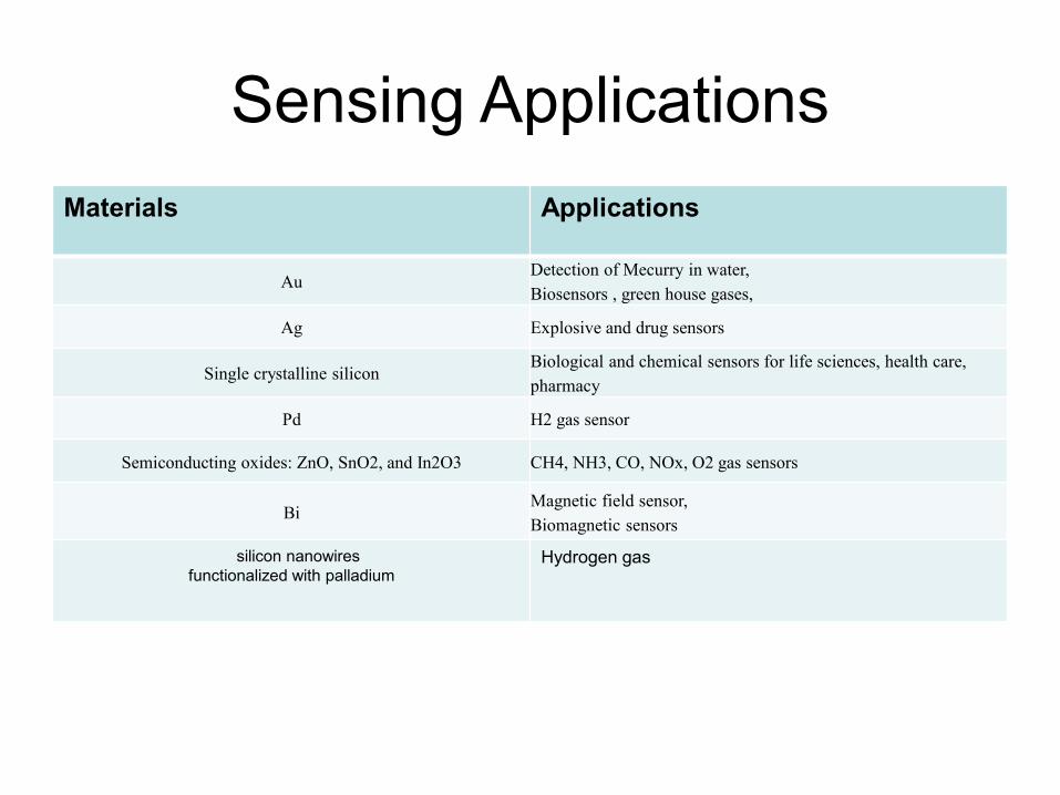
Sensing Applications
Materials Applications
AuDetection of Mecurry in water,
Biosensors , green house gases,
Ag Explosive and drug sensors
Single crystalline siliconBiological and chemical sensors for life sciences, health care,
pharmacy
Pd H2 gas sensor
Semiconducting oxides: ZnO, SnO2, and In2O3 CH4, NH3, CO, NOx, O2 gas sensors
BiMagnetic field sensor,
Biomagnetic sensors
silicon nanowires
functionalized with palladiumHydrogen gas

Nanowires and Energy
materials Applications
ZnO Piezoelectricity
Graphene coated with ZnO Solar cell
Semiconductor nanowires grown on
gold nanoparticles
Solar cell
Copper nanowires Flexible conductors
Semiconductor nanowires Light concentrator
CdS nanowires coated with CuS Solar cell
Silicon nanowires Hydrogen storage
Silicon nanowires grown on Stainless
steel
High capacity batteries
Doped ZnO nanowires Color centers, Single Photon Lasers
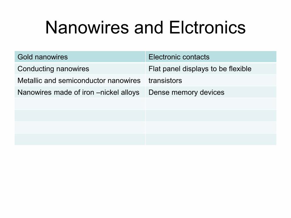
Nanowires and Elctronics
Gold nanowires Electronic contacts
Conducting nanowires Flat panel displays to be flexible
Metallic and semiconductor nanowires transistors
Nanowires made of iron –nickel alloys Dense memory devices

Applications
• Nanoelectronic Devices.
• Optoelectronic Devices Based on
Nanostructures
• Sensors
• Actuators
• NEMS
• Molecular and Biological Devices.
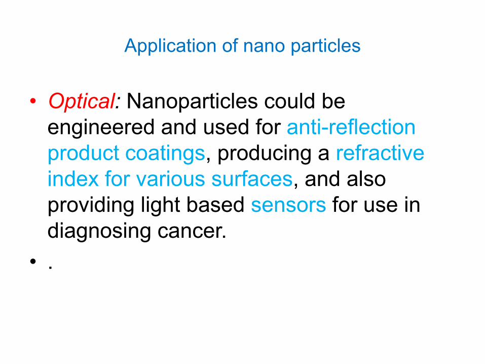
Application of nano particles
• Optical: Nanoparticles could be
engineered and used for anti-reflection
product coatings, producing a refractive
index for various surfaces, and also
providing light based sensors for use in
diagnosing cancer.
• .

Application of nano particles
• Magnetic. Nanoparticles have the potential
to increase the density of various storage
media, and also when magnetized they
can improve the detail and contrast of MRI
images as previously alluded to.

Application of nano particles
• Thermal. Specifically engineered particles
could improve the transfer of heat from
collectors of solar energy to their storage
tanks. They could also enhance the
coolant system currently used by
transformers in these types of processes.
Application of nano particles
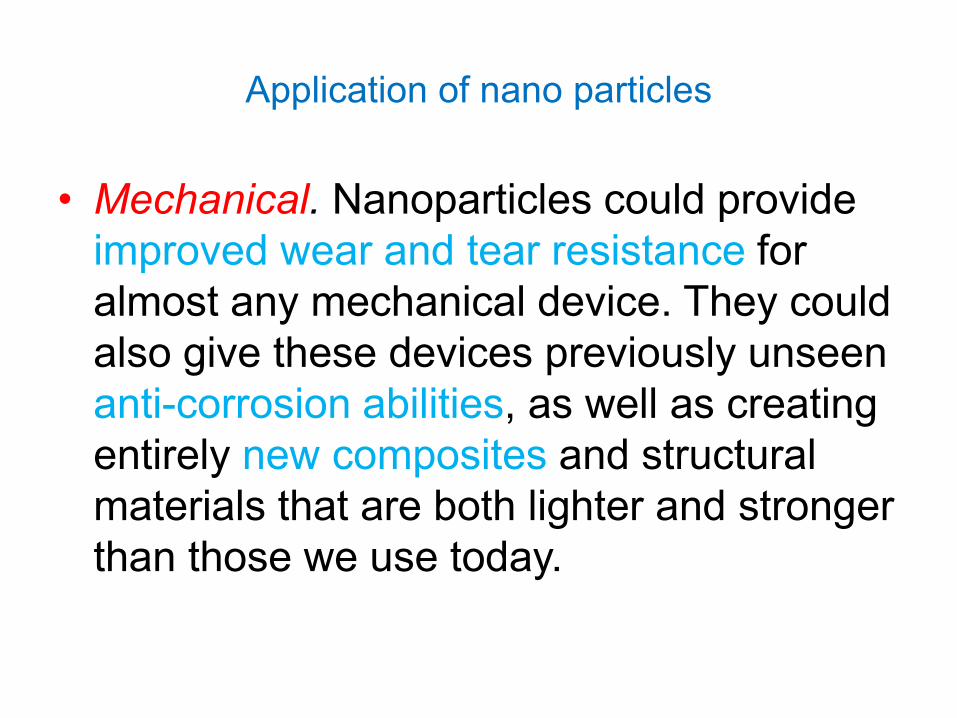
• Mechanical. Nanoparticles could provide
improved wear and tear resistance for
almost any mechanical device. They could
also give these devices previously unseen
anti-corrosion abilities, as well as creating
entirely new composites and structural
materials that are both lighter and stronger
than those we use today.

Application of nano particles
• Electronic. Because of their tiny size,
nanoparticles are inherently poised to aid
in the production of high performance
delicate electronics; they may provide not
only materials with a high rate of
conductivity, but also sleeker parts for
small consumer electronics like cell
phones. And when it comes to advertising,
nanoparticle electronics can create digital
displays that are more electricity-efficient,
less expensive to produce, brighter in

Nanoparticles and Energy
• Nanoparticle batteries would be longer-lasting and have
a higher energy density than those we use today.
• Metal nanoparticle clusters could also have revolutionary
applications for hydrogen storage
• They could also produce extremely efficient fuel cells by
acting as electrocatalysts for these devices.
• Nanoparticles may also pave the way for practical and
renewable energy; they have already demonstrated an
ability to improve solar panel efficiency many times over.

Nanoparticles and Biomedical
You may soon find that your wounds are
dressed with antibacterial coatings of silver
nanoparticles. Nanoparticles have also been
used to produce “quantum dots,” which can
detect diseases, as well as interactive foods
and drinks that change flavor and color
based on your tastes, or in some cases may
even alter their nutrient content based on
your state of health.

•Nanoparticles in polymer composite materials for application in baseball
structure to cars, .. airplane, satellites…
•Nanoparticles additives to or surface treatments of fabrics help them resist
wrinkling, staining, and bacterial growth,
•Nanoparticles or nanoscale thin films on eyeglasses, computer and camera
displays, windows, and other surfaces ..
•Nanoparticles materials in cosmetic products provide greater clarity or
coverage; cleansing..
•Nanoparticle materials in the food industry ..
•Nanosensors built into plastic packaging can warn against spoiled food.
•Nanoparticles are used to develop sensors to detect salmonella, pesticides,
and other contaminates on food

•Nanoparticle materials in automotive products include high-power rechargeable
battery systems and extended range.
•Nanoparticle materials make superior household products such as degreasers and
stain removers; environmental sensors, alert systems, air purifiers and filters;
antibacterial cleansers; and specialized paints and sealing products.
•Nanostructured ceramic coatings exhibit much greater toughness than
conventional wear-resistant coatings for machine parts. In 2000, the U.S. Navy
qualified such a coating for use on gears of air-conditioning units for its ships,
saving $20 million in maintenance costs over 10 years. Such coatings can extend
the lifetimes of moving parts in everything from power tools to industrial machinery.
•
•Nanoparticles are used increasingly in catalysis to boost chemical reactions.

•Nanoscale transistors that are faster, more powerful, and increasingly
energy-efficient; soon your computer’s entire memory may be stored on a
single tiny chip.
•Magnetic random access memory (MRAM) enabled by nanometer‐scale
magnetic tunnel junctions that can quickly and effectively save even
encrypted data during a system shutdown or crash, enable resume‐play
features, and gather vehicle accident data.
•Displays for many new TVs, laptop computers, cell phones, digital cameras,
and other devices incorporate nanostructured polymer films known as
organic light-emitting diodes, or OLEDs. OLED screens offer brighter images
in a flat format, as well as wider viewing angles, lighter weight, better picture
density, lower power consumption, and longer lifetimes.
•Other computing and electronic products include Flash memory chips for
iPod nanos; ultrar esponsive hearing aids; antimicrobial/antibacterial coatings

•Nanostructured materials are being pursued to greatly improve hydrogen
membrane and storage materials and the catalysts needed to realize fuel cells
for alternative transportation technologies at reduced cost. Researchers are also
working to develop a safe, lightweight hydrogen fuel tank.
•Various nanoscience-based options are being pursued to convert waste heat in
computers, automobiles, homes, power plants, etc., to usable electrical power.
•An epoxy containing carbon nanotubes is being used to make windmill blades
that are longer, stronger, and lighter-weight than other blades to increase the
amount of electricity that windmills can generate.
•Researchers are developing wires containing carbon nanotubes to have much
lower resistance than the high-tension wires currently used in the electric grid
and thus reduce transmission power loss.

•To power mobile electronic devices, researchers are developing thin-film solar
electric panels that can be fitted onto computer cases and flexible piezoelectric
nanowires woven into clothing to generate usable energy on-the-go from light,
friction, and/or body heat.
•Energy efficiency products are increasing in number and kinds of application.
In addition to those noted above, they include more efficient lighting systems
for vastly reduced energy consumption for illumination; lighter and stronger
vehicle chassis materials for the transportation sector; lower energy
consumption in advanced electronics; low-friction nano-engineered lubricants
for all kinds of higher-efficiency machine gears, pumps, and fans; light-
responsive smart coatings for glass to complement alternative heating/cooling
schemes; and high-light-intensity, fast-recharging lanterns for emergency
crews.

• Nanotechnology has the real potential to revolutionize a wide array of
medical and biotechnology tools and procedures so that they are more
personalized, portable, cheaper, safer, and easier to administer. Below are
some examples of important advances in these areas.
• Quantum dots are semiconducting nanocrystals that can enhance biological
imaging for medical diagnostics. When illuminated with ultraviolet light, they
emit a wide spectrum of bright colors that can be used to locate and identify
specific kinds of cells and biological activities. These crystals offer optical
detection up to 1,000 times better than conventional dyes used in many
biological tests, such as MRIs, and render significantly more information.
• Nanotechnology has been used in the early diagnosis of atherosclerosis, or
the buildup of plaque in arteries. Researchers have developed an imaging
technology to measure the amount of an antibody-nanoparticle complex that
accumulates specifically in plaque. Clinical scientists are able to monitor the
development of plaque as well as its disappearance following treatment
(see image).

Nanoelectronics DevicesCarbon nanotube field effect transistors (CNFET)
• A carbon nanotube device is similar to a MOSFET where a gate is used to control the flow of current through the device by varying the field through a channel. The new idea here is the mechanism of transport of electrons from the source to drain. Instead of having a channel whose field can be controlled by a gate electrode, these devices have a tiny tubular structure of carbon nanotube. Carbon nanotube with diameter 2nm have extremely low resistance and thus can carry large current without heating, so it could be use as interconnectors. It also has very high thermal conductivity means that they can also serve as heat sink i.e. allows heat to be rapidly transferred away from the chip.

Carbon Nanotube Single-Electron Transistor (SET)
Single-electron transistors (SETs) are transistors whose drain to source
current is composed of only one electron. With only one electron
traveling, the power consumption is greatly reduced.
It has been discovered that SETs will have a very tough time replacing
MOSFETs because of their low gain, high impedance, and higher
sensitivity to background noise
The SETs contribution is high charge sensitivity, while the MOSFETs
provide the gain and low impendence needs for real life application.
Another important application for SETs is charge-sensing applications
such as the readouts for both memories and charge-coupled devices in
metrology and astronomy where precision charge measurements are
required.

Electronic Devices
A Carbon nanotube field effect transistors (CNFET)


Electronic Devices
Single-Electron Transistors
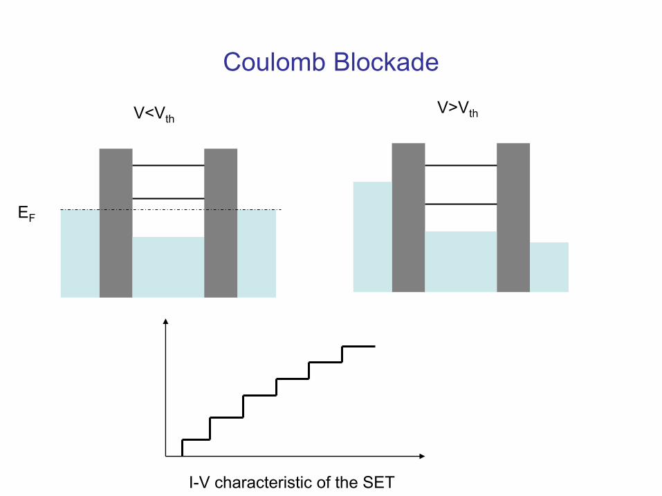
Coulomb Blockade
V<VthV>Vth
I-V characteristic of the SET
EF


The first gate is of a standard planar design that is used for the input of the transistor. The
second gate is a parallel plate type of gate, used to tune the background charge. The
arrows point to the small points where the source and drain make contact. These contact
points are the tunneling junctions that isolate the conduction island.

pnp device
ε is steepness of the barrier

CNT Switches
• Due to the thermal activation of electrons over the energy gap results in empty valence states and occupied conduction states.
• The off-state conductance of semiconductor CNT is non-zero, and it is depend on the temperature and the band gap.

Effects of Doping on CNT Structure
• The geometry, band structure, and binding
energies of CNT is strongly depend on the
doping of some atoms or molecules.
• The effects of hydrogen doping is very
depend on the pattern of hydrogenation.

Effects of Doping on CNT
O. Gulseren, et al. 2002
T. Yildirim, Phys. Rev.B, 64, pp
75404-1/, 2001
Hydrogen

Optoelectronic Devices
• Light emission from CNTs
IRThe transistor has two Schottky
barriers at the source and drain.
Electron and holes can inject into
the intrinsic CNT, inducing light
emission with wavelength of 1.5 -
2 micron. It was found that IR
luminescence emitted from a
very small region. Its position can
be controlled by applied gate
voltage. The intensity and the
shape of IR spot can be
monitored.
The IRL is optimized
when VG = VD/2 and the
source is grounded

Nanowires and Optoelectronic Devices
substrate
Semiconductor
NW
P type SNW
N type SNW GaN CdS CdSeelectrodes
ZnO NW
light

Buckytube Electro-
mechanical
NanoActuators
Baughman et al., Science 284, 1340 (1999)
~1% length change per volt

Memory device based on 2 layers of carbon nanotubes,
in which the top layer is suspended above the lower
layer. A 3D view, gold structures are the contacts, and
the black cubes are nonconductive supports
Conductivity and molecular perfection
allows nanotubes to be used as switches
and memory elements.

NEMS
• NEMS research involves design
prototyping, fabrication, control,
programming, and applications.
• Design of any NEMS or MEMS involves
Sensors, Actuators, and Control.

NEMS
• Sensors, which sense chemicals,
mechanical, electrical, and any other
physical changes, had so far very little
progress.
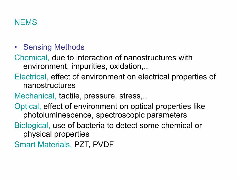
NEMS
• Sensing Methods
Chemical, due to interaction of nanostructures with environment, impurities, oxidation,..
Electrical, effect of environment on electrical properties of nanostructures
Mechanical, tactile, pressure, stress,..
Optical, effect of environment on optical properties like photoluminescence, spectroscopic parameters
Biological, use of bacteria to detect some chemical or physical properties
Smart Materials, PZT, PVDF
Sensors
• Tactile sensing using functionalized SPM cantilevers is investigated.
• Fluorescent probes with nano sizes are reported.
• Biological species like bacteria may be used to sense light or magnetic fields.
• Sensors technologies, in particular chemical and biochemical sensing are evolving very fast.
Sensors
• Nanotubes and nanowires are used to sense the chemicals and gases.
• Chemical sensors based on microscopic cantilevers are investigated. The detection mechanism is based on either by detecting the deflection of a cantilever caused by surface stresses that arise when a chemical species binds to one of the two opposing sides of the cantilever, or by measuring the shift in the resonance frequency of a vibrating cantilever when its mass increases because of the deposition of the molecules being detected.

Gas SensorsHow does a gas sensor work?
• Gaseous species are adsorbed at the
surface of materials (catalysts)
• Some physical properties of catalysts are
changed upon adsorption of gases
• By monitoring those physical parameters,
one can detect the gas type and measure
its concentration

Gas Ionization Sensors
1. The precise breakdown voltage provides the fingerprint for the gas to be identified; it is well established that at constant temperature and pressure every gas has a unique breakdown electric field.
2. Because this technique does not involve adsorption / desorption of gases, the sensor displays a fast response and is not limited by considerations of reversibility and recovery.

Methods of Operation
Breakdown Voltage
(Vb)
Blunt-tip AuNRs
or
Whisker/Al2O3-covered AuNRs
at the cathode
Tunneling Field-Ion Current
IFI = f(UI)
Whisker/Al2O3-covered AuNRs
at the anode
AuNRs are used as field-enhancing elements
(a) (b)
A
A
DC
DC
Ic or Ia
Ia or IcSMU #1
SMU #2
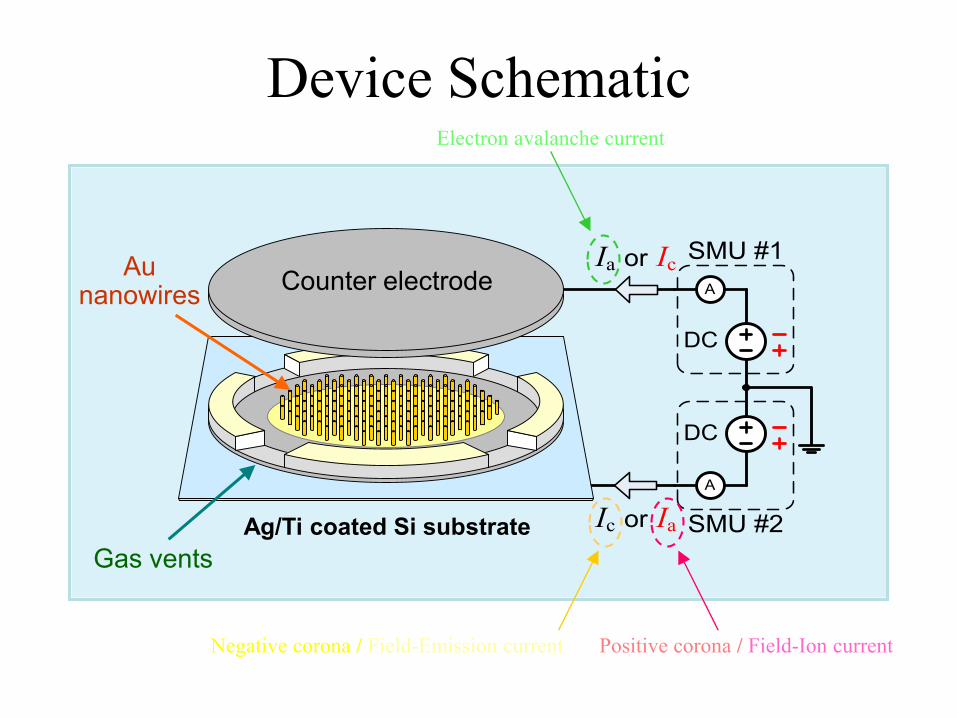
Device Schematic
Counter electrode
Gas vents
Au nanowires
Ag/Ti coated Si substrate
Positive corona / Field-Ion currentNegative corona / Field-Emission current
Electron avalanche current

Geometrical Field Enhancement
d
VFM macroscopic field
V
d
Geometrical/Mathematical models for
field enhancing: (top) definition of the
macroscopic field in a parallel-plate
capacitor; (right) enhancement factor
on a hemisphere on a post structure
resembling a nanotube or nanowire
R.G. Forbes et al.
Ultramicroscopy 95, 57–65 (2003).
M
loc
F
F
L
9.015.22.1
field-enhancement
factor
protrusion length to
base ratio
V
dFloc
2
L
VFloc field factor

200
250
300
350
400
450
500
550
0 2 4 6 8 10
Pressure (P ) [torr]
Bre
akd
ow
n v
olta
ge
(V
b)
[V]
0.E+00 1.E-04 2.E-04 3.E-04 4.E-04 5.E-04 6.E-04
Concentration [mol/liter]
O
Air
N
Ar
2
2
Sensor #1
Breakdown characteristics of Au-only device
Vb–P curves of the NWGIS (AuNWs at the cathode) for Ar, N2, Air and O2.
The minimum breakdown voltage (Vb)min, observed here, occurred within a
pressure range of 0.3 < P < 0.5 torr which is far less than the pressures at
which Vb is minimum in uniform fields.
R. B. Sadeghian & M. Kahrizi,
SNA 137, 248–255, (2007).

The Two-Step Field Enhancement Approach
rt2
l2
l1
r t1
1 1 1 1, t appE l r E
2 2 2 2 1 1 1, ,t t appE l r l r E
appE V d
d

Tunneling Field Ionization
He Atom
He+ ion
rtip
R
Cathode
Anode
He Atom
rtip
He+ ion
12
3
tipr
RM
Theory

µ-spheres
100 nm
Nanowhiskers

Tunneling Field Ionization on Semiconductors
EC
EV
EF
fS
f fS UI
atom
xc
Valence band
ES = Evac' erEvac
surface
states
lS
e-
c
T.T. Tsong, Surf. Sci. 85, 1–18 (with modifications).
Ic SU Ex ff
l
ef r
S
E
1/ 21/ 2exp I cD A U BE x
Theory
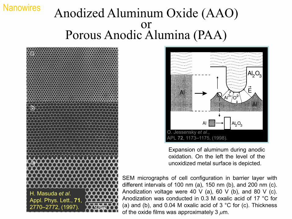
Anodized Aluminum Oxide (AAO)or
Porous Anodic Alumina (PAA)
Expansion of aluminum during anodic
oxidation. On the left the level of the
unoxidized metal surface is depicted.
O. Jessensky et al.,
APL 72, 1173–1175, (1998).
SEM micrographs of cell configuration in barrier layer with
different intervals of 100 nm (a), 150 nm (b), and 200 nm (c).
Anodization voltage were 40 V (a), 60 V (b), and 80 V (c).
Anodization was conducted in 0.3 M oxalic acid of 17 °C for
(a) and (b), and 0.04 M oxalic acid of 3 °C for (c). Thickness
of the oxide films was approximately 3 mm.
H. Masuda et al.
Appl. Phys. Lett., 71,
2770–2772, (1997).
Nanowires
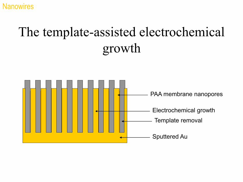
The template-assisted electrochemical
growth
PAA membrane nanopores
Sputtered Au
Electrochemical growth
Template removal
Nanowires

Self-Standing AuNWs
Nanowires

Super tips Tubular Structures
Nanowhiskers
Nanowires

Photographs
Film of vertically aligned freestanding
gold nanowire/nanorods bonded on an
Ag-Ti coated silicon substrate, after the
embedding template has been removed
A snapshot of the
Gas Ionization Sensor

Breakdown characteristics
200
250
300
350
400
450
500
550
0.01 0.1 1 10
Pressure (P ) [torr]
Bre
akdow
n v
oltage (
Vb
) [V
]
O
air
N
Ar
2
2
36
37
38
39
40
41
42
0.0001 0.001 0.01 0.1 1
Pressure (P ) [torr]
Bre
akdow
n V
oltage (
Vb
) [V
]
He
Ar
O2
Room temperature Vb – P characteristics of our sensor, in O2
, air, N2 and Ar, when the embedding template is completely
removed (semilog scale). The dashed lines show the average
Vb of each gas for P 1 torr.
Room temperature Vb – P characteristics of our sensor, in He,
Ar and O2, when the dissolution treatment was incomplete
(semilog scale). The breakdown voltages are considerably
reduced compared to the former case due to presence of
alumina on AuNWs.
Au-only Au/Al2O3 with whiskers

0
1
2
3
4
5
6
7
8
9
10
0 10 20 30 40 50
V (V)
I (
10
-5 A
)4E-06
0.01
0.09
37
Sensor #7
Full range I – V
(AuNWs at the cathode)
Fowler-
Nordheim
tunneling
Quasiballistic
emission
Formation of
coronabreakdown
Results

ZnO nanowires

Applications
E-Nose
Explosive & Poisonous
gases
Control
air quality
Vacuum
control

Device Optimization
I1 I2 I3 ...
DC
High FieldLow Field
Improved Vents Tilted Counter Electrode
Multigrid Electrode
Applications: Odor Sensors, Explosive &
Poisonous Gases, …
Grid of
Sensors
Pattern
Recognition
System
Analysis & Control
System
PreprocessorGas Flow
(Odor)

66
Biosensors
• AFM of Au-PS
colloidal crystal (Au
can’t be seen here –
too small)
• Ordered multilayers of
composites 18-20
layers
PS microspheres: 510 nm; Au: 5 nm
Vertical deposition 55oC, 3 days
Morphology of Au Nanostructures

67
• Sample prepared with 700 nm PS
Spheres – not annealed
• Nanorings and nanoholes present
• Aggregation effects around holes
•Size of holes is less than the size of
spheres
Results
Morphology cont’d
• Fabricated many samples – PS sphere sizes: 100 nm, 200 nm, 500 nm and 700 nm
• Resulted in hole and ring structures
• Ring structures are not continuous ring structures - made of nanoparticles which do not touch one another
• Some samples were annealed and some were not
• Observed aggregation effects around holes for certain samples
• Observed PS spheres not completely removed in some cases
• Nanohole/nanoring array prepared with 530 nm PS and 20 nm Au – more rings
• Sample annealed at 900C for 20 min
• Inset: enlarged image of a region where PS spheres were not completely removed. - Au nanoparticles are around and on the top of the spheres

68
Results
Morphology cont’d
• Sample prepared with 200 nm PS
Spheres – not annealed
• Nanohole present – evenly
distributed
• Sample prepared with 200 nm PS
Spheres – not annealed
• Nanoholes present – some imperfections

Gold Nanostructures

71
Results
UV-VIS Spectrum of a Nanohole/Nanoring Array -
Sensitivity of the Structure (l/n)
A) In water and B) 2-PROPANOL (sample annealed for 30 min at
110C)
Au LSPR band red-shifted by 8 nm in 2-propanol S = 340 nm/RIU
72
Results
Biomolecular Interactions cont’d
• ADDL deposited on
functionalized gold
structures
• Left in contact with
sensor platform for
24 hours
• Large shift of
LSPR band
observed Δλ = 30nm
Δλ = λ in PBS without ADDL – λ in
PBS with ADDL

73
Biomolecular Interactions cont’d
Spectra corresponding to the protein-antibody interaction:
A) spectrum of the functionalized substrate using Au that
was prepared in the lab B) spectrum of the antibody
adsorbed on the substrate C) spectrum of the previously
absorbed antibody followed by the adsorption of the protein
on the substrate
• Observed shift of +10 nm when antibody adsorbed
• After protein adsorption no additional shift but observed
shoulder around 600 nm
74
Spectrum corresponding to the protein sandwiched between two antibody
layers: A) Spectrum of the functionalized substrate with antibody and protein
adsorption – using Au that was prepared in the lab B) spectrum when an
additional antibody layer is adsorbed on the system corresponding to trace A
Biomolecular Interactions cont’d
Additional antibody layer results in shift of +10 nm

NEMS
• Actuators, are moving parts of any micro or nano devices.
• Powers are mechanical, electrical, optical or chemical, which among them electrical and optical are most convenient.
• CNT, nanowires, nano-cantilevers,… can be used as the actuators.
• Molecular actuators either from a single molecules or supramolecules are fabricated using chemical synthesis. They are atomically precise.

Nano cantilever

NEMS
• Electrical &Electromagnetic Actuators
Coulomb interactions including weak interactions
Capacitive interactions
Dipole- Dipole interactions
Dipole Interaction with Electric Field
Magnetic Field Interactions
Magnetic dipole-dipole interactions
Magnetostrictive Materials (ferromagnetic materials)
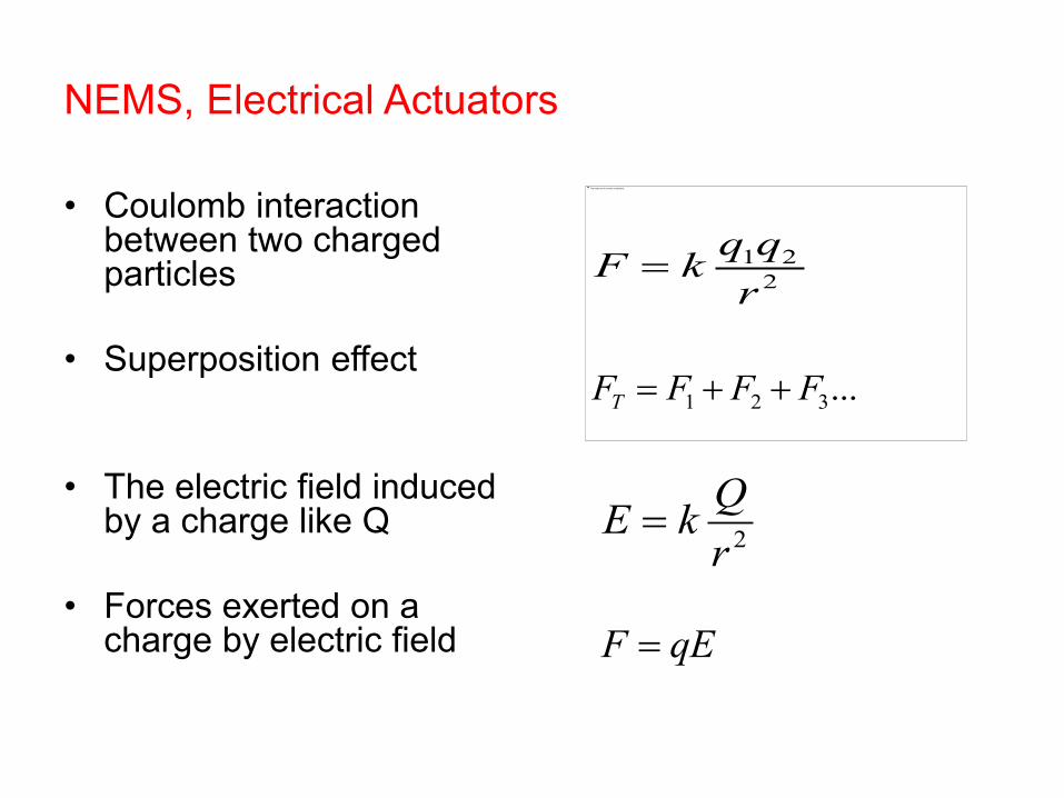
NEMS, Electrical Actuators
• Coulomb interaction between two charged particles
• Superposition effect
• The electric field induced by a charge like Q
• Forces exerted on a charge by electric field
2
21
r
qqkF
...321 FFFFT
2r
QkE
qEF

NEMS, Electrical Actuators
• The distribution of charges in a body is characterized by a parameter called dipole moment
p = LQ (p is a vector
directed from –ve
charge toward +ve
charge)
Applying electric field induces a torque T = p x E (T, p, and E are vectors)

NEMS, Electrical Actuators
F+ = EQsin(θ)
F- =- EQsin(θ) The net force is
zero, and as a
result of this
torque the rod will
rotate around
centerT =∑ r x F = -1/2 L Q Esin(θ) -1/2LQEsin(θ)
= - LQ E sin(θ)

NEMS, Electrical Actuators
• The energy of the two
dipoles p1 and p2 at
angles θ1and θ2
measured from the
line connecting the
dipoles is given by
3
21
3
21int
).)(.(3.
r
rprp
r
ppE eraction

NEMS, Electrical Actuators
• Similar to electric dipoles, there exist a magnetic dipole between the two magnetic poles.
• A current carrying loop of radius a induces a magnetic dipole moment m
• Electrons orbit around nucleus also induces current and dipole moments
2aIm
r
qvI
2
2
qvrIAm
NEMS, Electrical Actuators
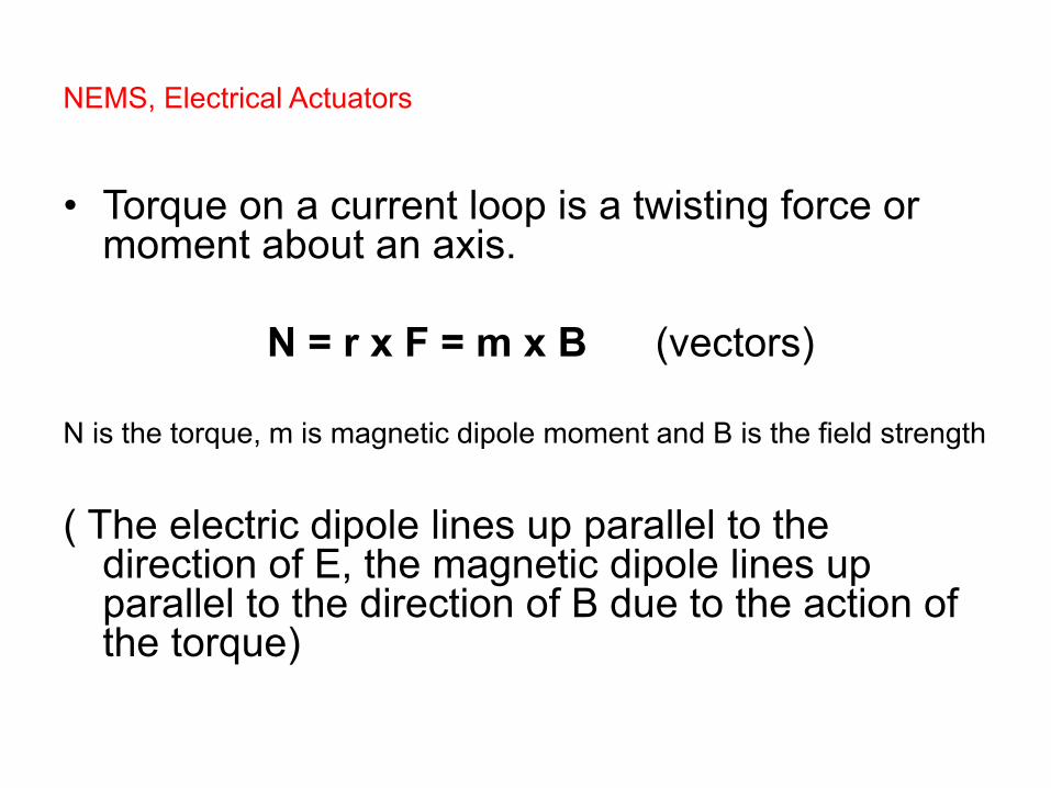
• Torque on a current loop is a twisting force or moment about an axis.
N = r x F = m x B (vectors)
N is the torque, m is magnetic dipole moment and B is the field strength
( The electric dipole lines up parallel to the direction of E, the magnetic dipole lines up parallel to the direction of B due to the action of the torque)

NEMS, Electrical Actuators
+-
-
-
- +
+
+
+
+
-
Electrophoresismigration of dispersed particles on a fluid under the influence of
an uniform electric field
Coulomb Interaction

NEMS, Electrical Actuators
+
+
+
+
+ - - - - - -
-
-+
+
Dielectrophoresismigration of dispersed particles in a fluid under the influence
of a non-uniform electric field

NEMS, Electrical Actuators
0o
27
0o
180o
90o
-Q Q+
E
Electrorotation

NEMS, Electrical Actuators

NEMS, Optical forces
• Optical actuation is due to:
Direct conversion of optical energy to mechanical (thermal) energy
The interaction of Electric component of light with the charged particles
( Laser tweezers and laser spanners)
Molecular or Structural changes in nanostructures, cis-transisomerization
Photostrictive Materials (opto-piozoelectric)
Photorefractive crystals; Actuation occurs as a result of mechanical deformation of the crystal caused by photogenerated electric charge distribution due to piezoelectric effect.

NEMS
Isomerization
• Isomers are molecules having the same
atoms and the same bonds but different
equilibrium structure (geometry).
• Isomers can switch from one structure to
other if they subjected to external stimuli
like light, electric field, heat,…

NEMS
• The rotation happens as the light causes a cis-
trans isomerization. The resulting conformation
is unstable and spontaneously changes to a
more energetically-favorable conformation,
continuing the rotation.
• [cis-trans is a change of shape of the molecule
from a state in which two groups (of atoms) are
on the same side of a bond (cis) to another in
which the groups are on opposite sides of the
bond (trans)]
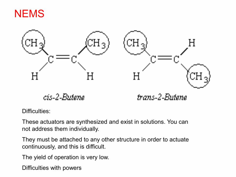
NEMS
Difficulties:
These actuators are synthesized and exist in solutions. You can
not address them individually.
They must be attached to any other structure in order to actuate
continuously, and this is difficult.
The yield of operation is very low.
Difficulties with powers

NEMS
Cantilevers
• An essential components to MEMS/NEMS is a cantilever which can actuate and be controlled by applied actuation forces.
• The actuation force could be electrostatic, electromagnetic or optical.
• The cantilever can be integrated with associated electronic/optoelectronic of a system.
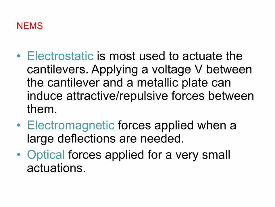
NEMS
• Electrostatic is most used to actuate the cantilevers. Applying a voltage V between the cantilever and a metallic plate can induce attractive/repulsive forces between them.
• Electromagnetic forces applied when a large deflections are needed.
• Optical forces applied for a very small actuations.
NEMS
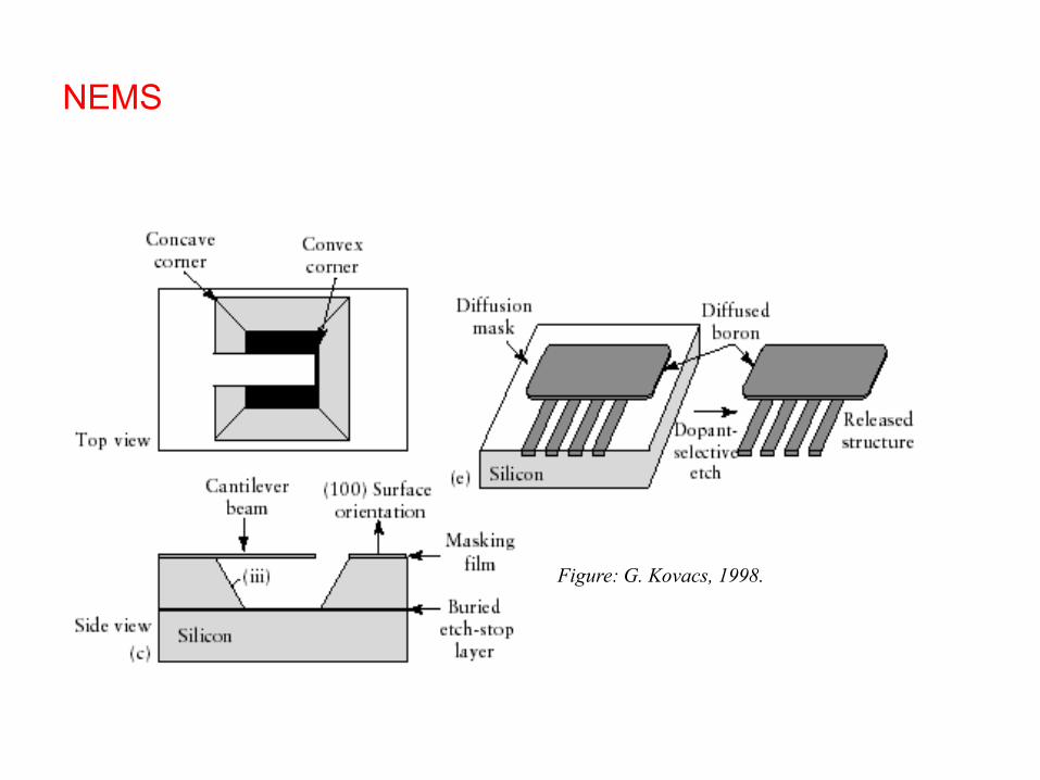
Figure: G. Kovacs, 1998.

NEMS
Many formula applied for micro structures are not adequate for structures in nano scale among them:
a) Van der Waals forces: has a significant contribution to actuation process of nano cantilever, it is attractive or repulsive in nature. It is strongly sensitive to the geometry of the structure.
b) Casimir force: understood through Quantum Field Theory. According to this theory the vacuum is not empty, filled with virtual particles, continuously created and annihilated. This fluctuation induce a force between bodies separated by distances less than a micron. Again is strongly depended on the geometry and boundary conditions.
NEMS
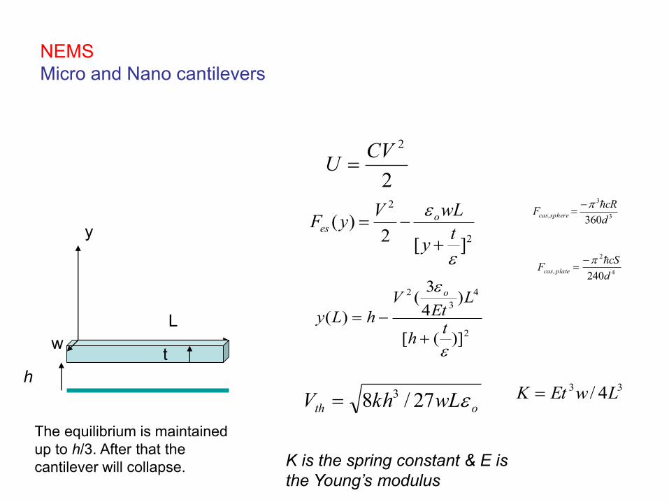
Micro and Nano cantilevers
2
2CVU
2
2
][2
)(
e
e
ty
wLVyF o
es
2
4
3
2
)]([
)4
3(
)(
e
e
th
LEt
V
hLy
o
4
2
,240d
cSF platecas
3
3
,360d
cRF spherecas
L
w
y
t
oth wLkhV e27/8 333 4/ LwEtK
K is the spring constant & E is
the Young’s modulus
The equilibrium is maintained
up to h/3. After that the
cantilever will collapse.
h
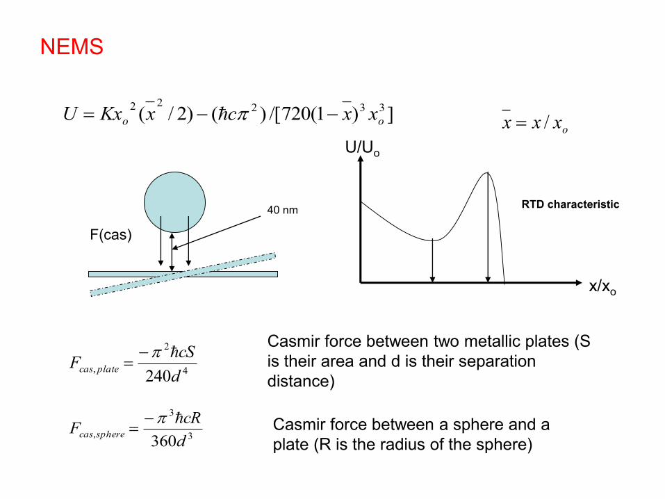
NEMS
3
3
,360d
cRF spherecas
4
2
,240d
cSF platecas
F(cas)
Casmir force between two metallic plates (S
is their area and d is their separation
distance)
Casmir force between a sphere and a
plate (R is the radius of the sphere)
])1(720/[)()2/( 33222
oo xxcxKxU oxxx /
40 nm
U/Uo
x/xo
RTD characteristic

NEMS
• Casmir force is dependent on the geometry of
the structures. Can be engineered to make nano
devices.
• As an example a nonlinear mechanical
oscillators and switches can be fabricated using
a sphere placed over a plate. As the plate moves
under elastic forces the structure oscillates
around the equilibrium (local minima) and can
switch between the minimum and maximum
positions.

NEMS
Micro and Nano cantilevers
Y(max)
Quantized motion of nanocantilever
Nano cantilever when are double-
clamped the van der Waals has a
very little effect however another
characteristic will show up. The
quantized mechanical movement of
the cantilever. Each time an electron
tunnel through the CNT (an
additional electrostatic
contribution), its deflection changes
in discrete steps.
NEMS
• Control:
• It is demonstrated that with the
combinations of sensors and power
sources one can control the behavior of
these nanodevices
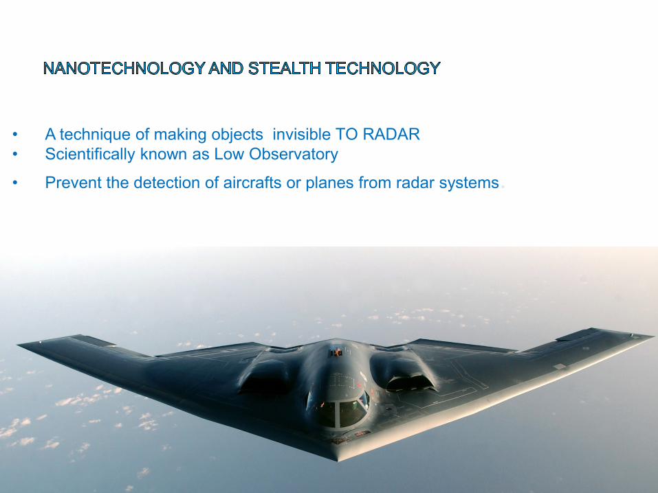
• A technique of making objects invisible TO RADAR
• Scientifically known as Low Observatory
• Prevent the detection of aircrafts or planes from radar systems.
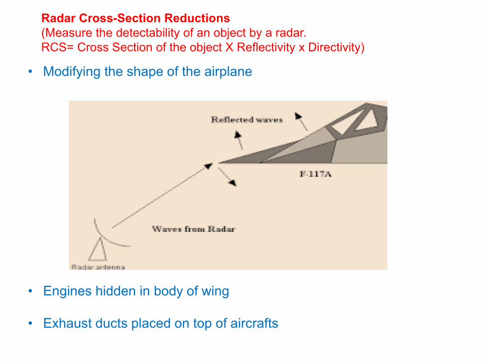
• Modifying the shape of the airplane
• Engines hidden in body of wing
• Exhaust ducts placed on top of aircrafts
Radar Cross-Section Reductions
(Measure the detectability of an object by a radar.
RCS= Cross Section of the object X Reflectivity x Directivity)
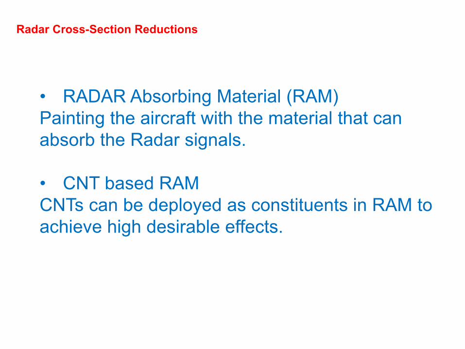
Radar Cross-Section Reductions
• RADAR Absorbing Material (RAM)
Painting the aircraft with the material that can
absorb the Radar signals.
• CNT based RAM
CNTs can be deployed as constituents in RAM to
achieve high desirable effects.

Production:
Carbon nanotube type used : CM95/MWNT
Diameter : 0.01-0.015 μm
Length : 10-20 μm
Formulations used : 0.1, 0.5 and 1.0% (w/w) of CNT
dispersed in the epoxy resin.
To achieve more homogenous dispersion, ultrasonic
homogenizer shoud be used.
Resin/CNT Composites
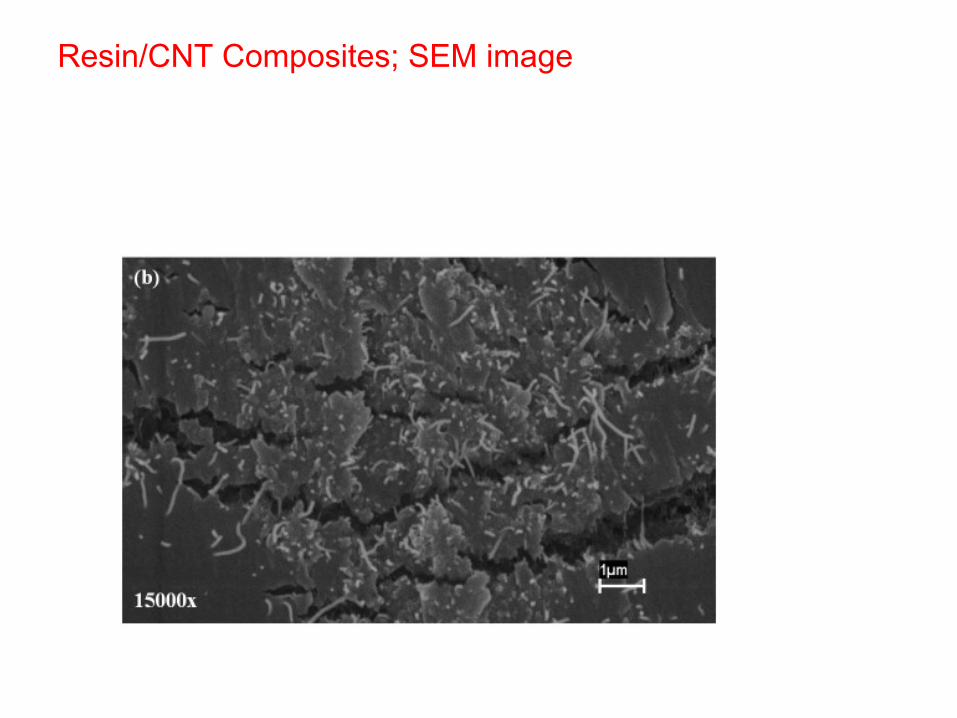
Resin/CNT Composites; SEM image
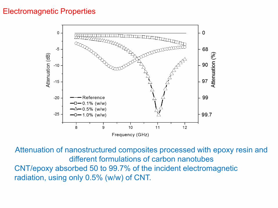
Electromagnetic Properties
Attenuation of nanostructured composites processed with epoxy resin and
different formulations of carbon nanotubes
CNT/epoxy absorbed 50 to 99.7% of the incident electromagnetic
radiation, using only 0.5% (w/w) of CNT.

• Cathode– Generally made of graphite
and other conductive additives.
• Anode– a layered transition metal
oxide
(Lithium cobalt oxide etc. )
• Electrolyte– Through which lithium ions
shuttles between the cathode and anode
Nanotechnology and Batteries

Improvements
• More energy storage and long duration of
power supply.
• Shorter charging times.
• Durability.
• Resistance to fire hazards.

Applying Nanotechnology
• Faster intercalation of Li ions can be facilitated by using nanosized materials for electrodes, which offer high surface areas and short diffusion paths, and hence faster storage and delivery of energy
• Nanosizing the anode materials can make the anode to have short mass and charge pathways to allow easier transport of both lithium ions and electrons, resulting in high reverse capacity and deliver at a faster rate.
• Nanostructuring of solid electrolytes has proven to improve the lithium ion conductivity, – for example, when the conventional bulk lithium thiophosphate
electrolyte was made nanoporous, it could conduct lithium ions 1000 times faster.

Nanotechnology and Hydrogen Storage
Advantages
• Higher energy per unit mass (>142 MJ kg-1 compare to 47 MJ kg-1 for a liquid hydrocarbon)
• Cleanest energy carrier (H2O is burning by-product compare to CO2 for hydrocarbons)
Disadvantages
• Low energy density per unit volume as it is a low density gas.
• Challenging onboard storage

Hydrogen Storage: physisorption
• Accumulation of hydrogen molecules on and between surfaces of
materials without any chemical reaction. H2 molecules are adsorbed
to host material surface by van der Waals force

Hydrogen Storage: Chemisorption
• Hydrogen atoms penetrate into interstitial site of the host materials
LaNi5, ZrNi, Mg2Ni; metallic hydride.
• Hydrogen atoms form covalent bonds with host material atoms like
Si, ZnO; complex hydride.
• b: hydrogen molecules split into atoms in
presence of catalyst
• c: in moderate pressure H atom take random
locations
• d: in high pressure they would fill all the
interstitial sites.
Nanowries and hydrogen storage
• The problem with the physisorption method is that
they can only occur at cryogenic temperatures which
are difficult to reach.
• On the other hand, the chemisorption methods are
fast and they need to be controlled so that they can be
used for practical purposes.
• The percentage of hydrogen that can be stored
depends upon individual type of nanowires like for
ZnO, ZnS, Ge, Si etc.

Hydrogen Storage: Silicon Nanowires
• It can be seen in the figure that the body of structures is made of closely stacked
nano plates, make them suitable for the hydrogen storage. The hydrogen can be
stored via physisorption (in space between the nano plates), as well as chemisorption
(attached to the dangling bonds on the surface of nano plates).
a) b) c)
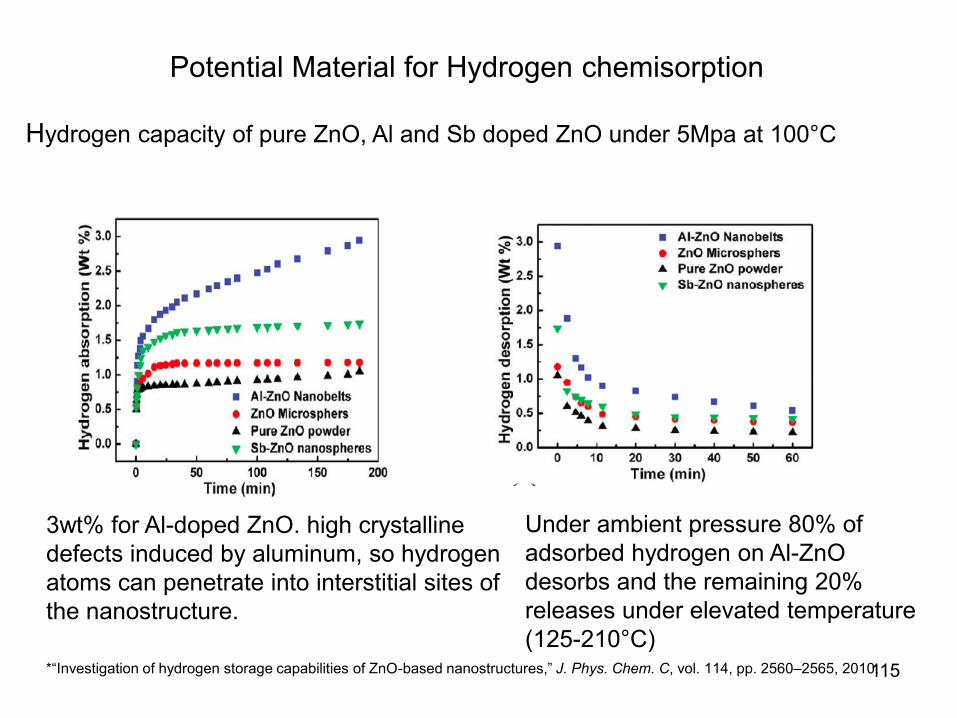
Potential Material for Hydrogen chemisorption
Hydrogen capacity of pure ZnO, Al and Sb doped ZnO under 5Mpa at 100°C
3wt% for Al-doped ZnO. high crystalline
defects induced by aluminum, so hydrogen
atoms can penetrate into interstitial sites of
the nanostructure.
Under ambient pressure 80% of
adsorbed hydrogen on Al-ZnO
desorbs and the remaining 20%
releases under elevated temperature
(125-210°C)*“Investigation of hydrogen storage capabilities of ZnO-based nanostructures,” J. Phys. Chem. C, vol. 114, pp. 2560–2565, 2010. 115
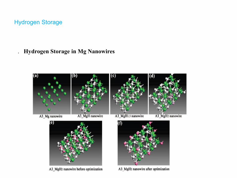
Hydrogen Storage
. Hydrogen Storage in Mg Nanowires

Nanotechnology and Solar Cell:
Effect of metal nanoparticles on polymers solar cell

Colloidal solutions of gold nanopartcles

Ag and Au nanoparticles

Local Surface Plasmonic Rresonance

Absorption bands of gold NP in water
Numbers represent 2R (nm)


Molecular Devices
• This is an inter/multidisciplinary research
field, engineering, biology, chemistry, and
physics.
• So we skip all (most of) the
chemical/biological terms.
• In this field most terms related to atomic
structures in semiconductors will be
replaced by molecular structures.

Molecular Devices
For example in band structures:
• Ec will be replaced by highest occupied molecular orbit (HOMO)
• Ev will be replaced by lowest unoccupied molecular orbit (LUMO)
• Metallic contacts are replaced by conjugated linear polymeric systems.
• Chemical substitutions will replace the doping in semiconductors.
• Molecular orbitals define the band gap.
• Individual atoms and the replacement will control all physical, mechanical, chemical, optical properties of the devices.

Molecular Devices
• Unlike the semiconductor electronic circuits
where adding a branch does not change the
electrical properties of the individual elements,
adding a new branch to a molecule creates a
new molecule with different electrical properties.
• So, the Ohm’s law and Kirchhoff's law can not
be applied for molecular circuits.
• As a result, the electrical properties of molecular
systems can be easily engineered.

Molecular Transistor
LUMO HOMO

Molecular Machines
• In common with their macroscopic counterparts,
a molecular machine is characterized by several
criteria. These are:
• the type of energy needed to make it work
• the nature of the movement during which work is
done or energy is transformed
• the way it can be controlled
• the ability to repeat its operation
• the time needed for a useful action.

Molecular Machines
• Catenanes, Rotaxanes and knots are
topologically molecular objects which are
well known to chemists for a long time.
However, these novel chemical species
received special attention in recent years
as it was found their places in the area of
nanosciences and nanotechnology, and an
emerging new field of research called
molecular machines and motors.

Molecular Machines

Molecular Machines
• Catenanes: Structures are joined bracelets
linked through each other. Their polymers, which
consist of chained together are called
polycatenanes
• Thus a [2] catenane has two rings and a [3]
polycatenane has three rings. Two-bracelet
catenanes ([2] catenanes) are useful because
each bracelet can be rotated around the other.

Molecular Machines
• Rotaxane: In this structure a central rod holds the axle to the superstructure through a collar, and dumbbell structures are at each end to stop the collar falling off. The molecular equivalents of these structures are called rotaxanes. Rotaxanes are of particular interest because the collar structure can often be moved by some external force and used as a molecular switch . The principle behind using rotaxanes as molecular switches is the ability to move the collar under some external influence. If the collar can be switched back and forth from each site 's' then it acts as a switch.

Molecular Machines
Rotaxane Catenane
S S
S S

Molecular Machines (Motors)
• A molecular machine is a multicomponent system in which the reversible movement of the components can be controlled by an external stimulus (S). Known examples of molecular machines includes nondegenerate rotaxanes (Type I), nondegenerate catenanes (Type II), as well as pseudorotaxanes (Type III). Control of the motions of the components in those systems has been introduced, which results in a change in properties which produce a signal that allows the operation of the machine to be monitored. The outside stimuli can be photons, electrons, or chemical species, to generate photochemically-, electrochemically- and chemically-driven molecular machines, respectively.

Molecular Machines

Molecular Machines

Molecular Machines

Molecular Machines

Molecular Machines

Molecular Machines
Molecular Machines

Molecular Machines

Molecular Machines

Molecular Machines

Molecular Machines
• Researches are done on the switches composed from the single molecules called molecular switches.
• There are various molecular switches that work using electricity, light, heat, protons or ions as external stimuli.
• Attentions are paid to catenanes which have a structure of two macrocycles which mechanically interlocked and move from the state A to the Bby the external stimulus.

Molecular Machines
The chemically and electrochemically triggered redox switching of 2 catenanes.

Molecular Machines
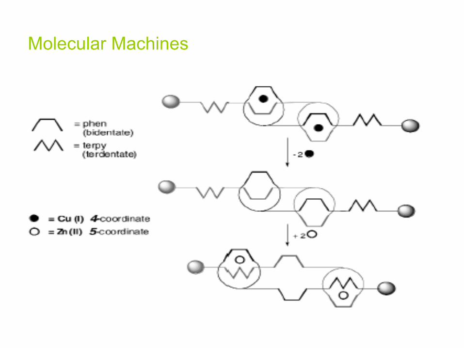
CN-
Cu+
Molecular Machines
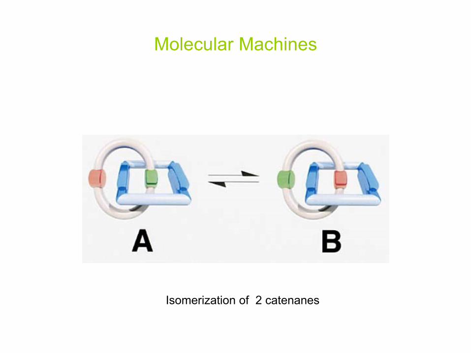
Isomerization of 2 catenanes
Molecular Machines
CH3OC
H3
S
CH3
H3C

Molecular Machines
• Parts of molecular machines: a molecular
paddle system,
Molecular Machines

Molecular Machines
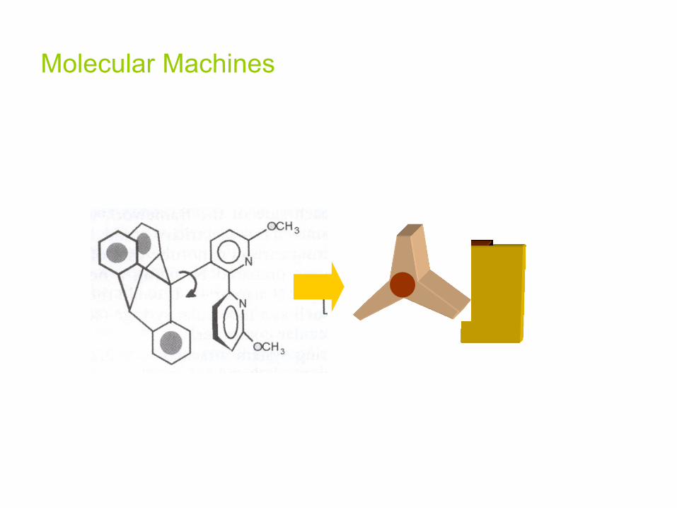
Molecular Machines
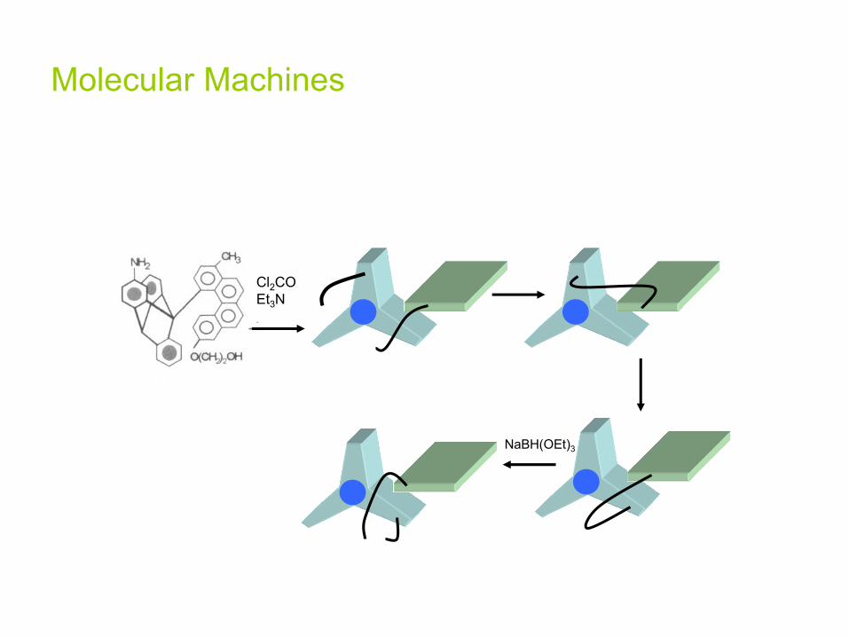
Molecular Machines
Cl2CO
Et3N
NaBH(OEt)3

Molecular Machines
CH3OC
H3
S
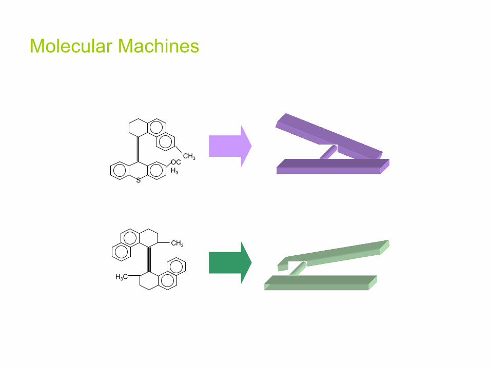
hv, 300nm
hv, 250nm
X
X
M-CisP-trans
M-transP-Cis
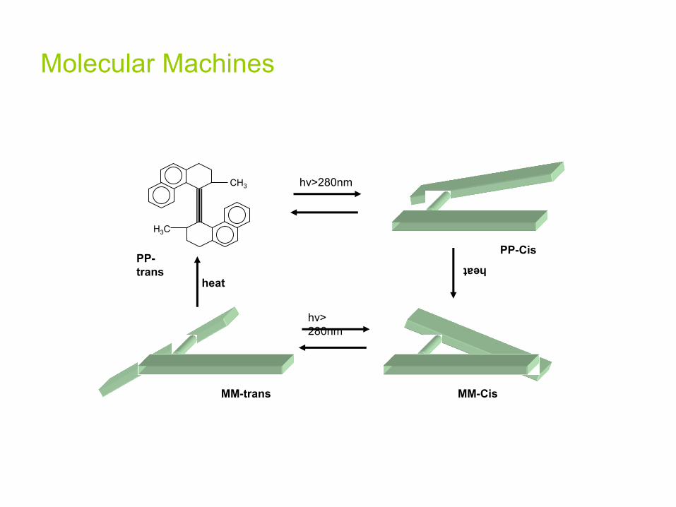
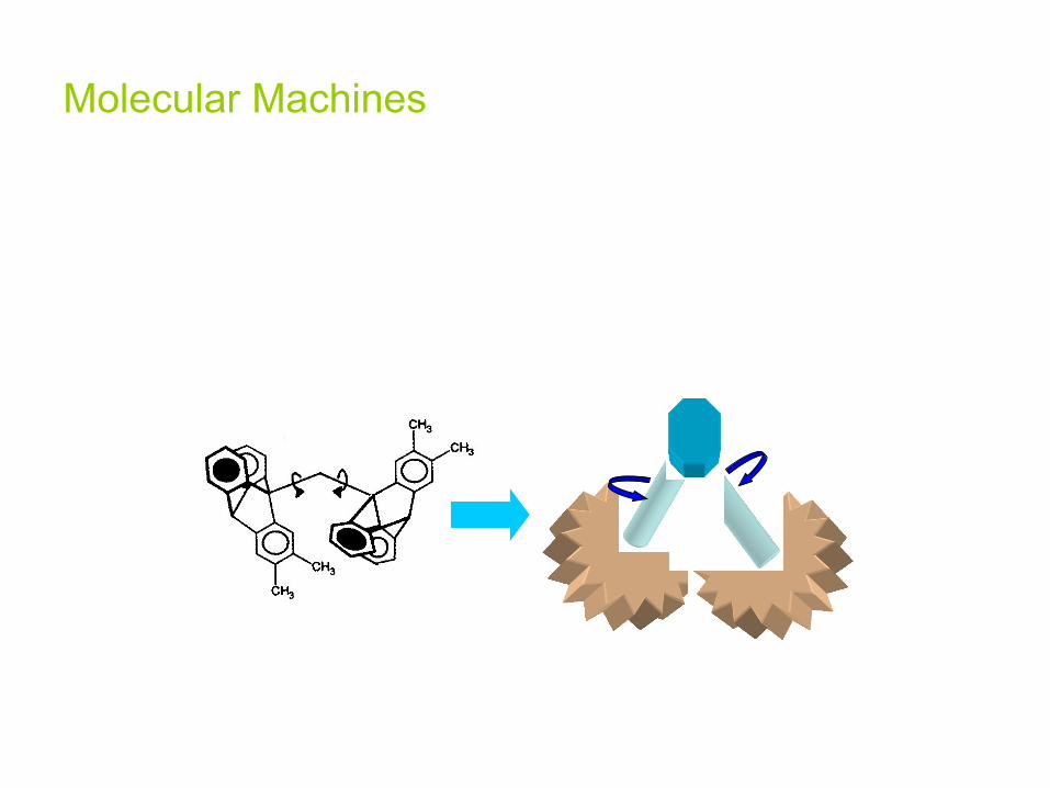
Molecular Machines
CH3
H3C
hv>
280nm
hv>280nm
heat
heat
PP-Cis
MM-CisMM-trans
PP-
trans
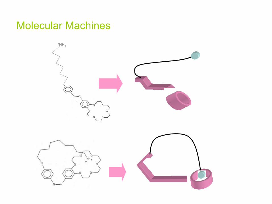
Molecular Machines
+NH3


![DNA Nanodevices based on i motif structuresdnatec09/presentations/2009_05_15_dnatec09... · DNA Nanodevices based on i‐motif structures ... Hao Yan [hao.yan@asu.edu] Challenges](https://static.fdocuments.us/doc/165x107/5c7f16b709d3f2aa3f8c1a71/dna-nanodevices-based-on-i-motif-structures-dnatec09presentations20090515dnatec09.jpg)