2736 IEEE JOURNAL OF SOLID-STATE CIRCUITS, VOL. 42,...
9
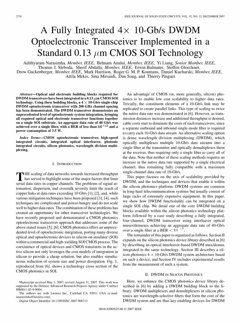
2736 IEEE JOURNAL OF SOLID-STATE CIRCUITS, VOL. 42, NO. 12, DECEMBER 2007 A Fully Integrated 4 10-Gb/s DWDM Optoelectronic Transceiver Implemented in a Standard 0.13 m CMOS SOI Technology Adithyaram Narasimha, Member, IEEE, Behnam Analui, Member, IEEE, Yi Liang, Senior Member, IEEE, Thomas J. Sleboda, Sherif Abdalla, Member, IEEE, Erwin Balmater, Steffen Gloeckner, Drew Guckenberger, Member, IEEE, Mark Harrison, Roger G. M. P. Koumans, Daniel Kucharski, Member, IEEE, Attila Mekis, Sina Mirsaidi, Dan Song, and Thierry Pinguet Abstract—Optical and electronic building blocks required for DWDM transceivers have been integrated in a 0.13 m CMOS SOI technology. Using these building blocks, a 4 10-Gb/s single-chip DWDM optoelectronic transceiver with 200 GHz channel spacing has been demonstrated. The DWDM transceiver demonstrates an unprecedented level of optoelectronic system integration, bringing all required optical and electronic transceiver functions together on a single SOI substrate. An aggregate data rate of 40 Gb/s was achieved over a single fiber, with a BER of less than and a power consumption of 3.5 W. Index Terms—CMOS optoelectronic transceiver, high-speed integrated circuits, integrated optical interleaver, photonic integrated circuits, silicon photonics, wavelength division multi- plexing. I. INTRODUCTION T HE scaling of data networks towards increased throughput has served to highlight some of the major factors that limit serial data rates in copper channels. The problems of signal at- tenuation, dispersion, and crosstalk severely limit the reach of copper links at data rates exceeding 10 Gb/s [1], [2], and, while various mitigation techniques have been proposed [3], [4], such techniques are complicated and power-hungry and do not scale well to higher data rates. The combination of these problems has created an opportunity for other transceiver technologies. We have recently proposed and demonstrated a CMOS photonics optoelectronic transceiver approach that addresses some of the above stated issues [5], [6]. CMOS photonics offers an unprece- dented level of optoelectronic integration, porting many diverse optical and optoelectronic devices to silicon-on-insulator (SOI) within a commercial and high-yielding SOI CMOS process. The coexistence of optical devices and CMOS transistors in the ac- tive silicon not only leverages the cost models of integration in silicon to provide a cheap solution, but also enables simulta- neous reduction of system size and power dissipation. Fig. 1, reproduced from [6], shows a technology cross section of the CMOS photonics in SOI. Manuscript received May 1, 2007; revised August 31, 2007. This work was supported by the Defense Advanced Research Projects Agency under Contract HR0011-05-9-0004. The authors are with Luxtera Inc., Carlsbad CA 92011 USA (e-mail: [email protected]). Digital Object Identifier 10.1109/JSSC.2007.908713 An advantage of CMOS (or, more generally, silicon) pho- tonics is to enable low cost scalability to higher data rates. Trivially, the constituent elements of a 10-Gb/s link may be replicated to create parallel links. This type of scaling to twice the native data rate was demonstrated in [6]. However, as trans- mission distances increase and additional throughput is desired, cable costs start to dominate the costs of such transceivers, since a separate outbound and inbound single-mode fiber is required to carry each 10-Gb/s data stream. An alternative scaling option is dense wavelength division multiplexing (DWDM), which optically multiplexes multiple 10-Gb/s data streams into a single fiber at the transmitter and optically demultiplexes them at the receiver, thus requiring only a single fiber to carry all of the data. Note that neither of these scaling methods requires an increase in the native data rate supported by a single electrical channel, thus remaining fully compatible with a maximum single-channel data rate of 10-Gb/s. This paper focuses on the axis of scalability provided by DWDM, and the techniques and devices that enable it within the silicon photonics platform. DWDM systems are common in long-haul telecommunication systems but usually consist of large racks of extremely expensive equipment. In this paper, we show how DWDM functionality can be integrated on a single SOI chip. We detail one of the core DWDM building blocks available within the silicon photonics technology plat- form followed by a case study describing a fully integrated, four-channel, DWDM transceiver using interleaver optical muxes/demuxes achieving an aggregate data rate of 40-Gb/s over a single fiber at a BER . The remainder of this paper is organized as follows. Section II expands on the silicon photonics device library described in [6] by describing an optical interleaver-based DWDM mux/demux integrated in the same technology. Section III describes a sil- icon photonics 4 10-Gb/s DWDM system architecture based on such a device, and Section IV includes experimental results from the measurement of such a system. II. DWDM IN SILICON PHOTONICS Here, we enhance the CMOS photonics device library de- scribed in [6] by adding a DWDM building block to the li- brary. DWDM multiplexers and demultiplexers in silicon pho- tonics are wavelength-selective filters that form the core of the DWDM system and are thus key enabling devices for DWDM 0018-9200/$25.00 © 2007 IEEE
Transcript of 2736 IEEE JOURNAL OF SOLID-STATE CIRCUITS, VOL. 42,...
2736 IEEE JOURNAL OF SOLID-STATE CIRCUITS, VOL. 42, NO. 12, DECEMBER 2007
A Fully Integrated 4 10-Gb/s DWDMOptoelectronic Transceiver Implemented in a
Standard 0.13 �m CMOS SOI TechnologyAdithyaram Narasimha, Member, IEEE, Behnam Analui, Member, IEEE, Yi Liang, Senior Member, IEEE,
Thomas J. Sleboda, Sherif Abdalla, Member, IEEE, Erwin Balmater, Steffen Gloeckner,Drew Guckenberger, Member, IEEE, Mark Harrison, Roger G. M. P. Koumans, Daniel Kucharski, Member, IEEE,
Attila Mekis, Sina Mirsaidi, Dan Song, and Thierry Pinguet
Abstract—Optical and electronic building blocks required forDWDM transceivers have been integrated in a 0.13 m CMOS SOItechnology. Using these building blocks, a 4 10-Gb/s single-chipDWDM optoelectronic transceiver with 200 GHz channel spacinghas been demonstrated. The DWDM transceiver demonstrates anunprecedented level of optoelectronic system integration, bringingall required optical and electronic transceiver functions togetheron a single SOI substrate. An aggregate data rate of 40 Gb/s wasachieved over a single fiber, with a BER of less than 10
12 and apower consumption of 3.5 W.
Index Terms—CMOS optoelectronic transceiver, high-speedintegrated circuits, integrated optical interleaver, photonicintegrated circuits, silicon photonics, wavelength division multi-plexing.
I. INTRODUCTION
THE scaling of data networks towards increased throughputhas served to highlight some of the major factors that limit
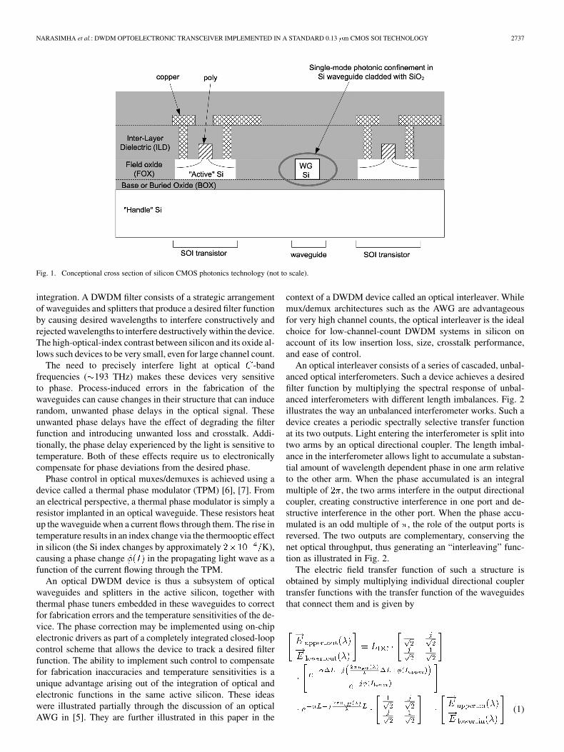
serial data rates in copper channels. The problems of signal at-tenuation, dispersion, and crosstalk severely limit the reach ofcopper links at data rates exceeding 10 Gb/s [1], [2], and, whilevarious mitigation techniques have been proposed [3], [4], suchtechniques are complicated and power-hungry and do not scalewell to higher data rates. The combination of these problems hascreated an opportunity for other transceiver technologies. Wehave recently proposed and demonstrated a CMOS photonicsoptoelectronic transceiver approach that addresses some of theabove stated issues [5], [6]. CMOS photonics offers an unprece-dented level of optoelectronic integration, porting many diverseoptical and optoelectronic devices to silicon-on-insulator (SOI)within a commercial and high-yielding SOI CMOS process. Thecoexistence of optical devices and CMOS transistors in the ac-tive silicon not only leverages the cost models of integration insilicon to provide a cheap solution, but also enables simulta-neous reduction of system size and power dissipation. Fig. 1,reproduced from [6], shows a technology cross section of theCMOS photonics in SOI.
Manuscript received May 1, 2007; revised August 31, 2007. This work wassupported by the Defense Advanced Research Projects Agency under ContractHR0011-05-9-0004.
The authors are with Luxtera Inc., Carlsbad CA 92011 USA (e-mail:[email protected]).
Digital Object Identifier 10.1109/JSSC.2007.908713
An advantage of CMOS (or, more generally, silicon) pho-tonics is to enable low cost scalability to higher data rates.Trivially, the constituent elements of a 10-Gb/s link may bereplicated to create parallel links. This type of scaling to twicethe native data rate was demonstrated in [6]. However, as trans-mission distances increase and additional throughput is desired,cable costs start to dominate the costs of such transceivers, sincea separate outbound and inbound single-mode fiber is requiredto carry each 10-Gb/s data stream. An alternative scaling optionis dense wavelength division multiplexing (DWDM), whichoptically multiplexes multiple 10-Gb/s data streams into asingle fiber at the transmitter and optically demultiplexes themat the receiver, thus requiring only a single fiber to carry all ofthe data. Note that neither of these scaling methods requires anincrease in the native data rate supported by a single electricalchannel, thus remaining fully compatible with a maximumsingle-channel data rate of 10-Gb/s.
This paper focuses on the axis of scalability provided byDWDM, and the techniques and devices that enable it withinthe silicon photonics platform. DWDM systems are commonin long-haul telecommunication systems but usually consist oflarge racks of extremely expensive equipment. In this paper,we show how DWDM functionality can be integrated on asingle SOI chip. We detail one of the core DWDM buildingblocks available within the silicon photonics technology plat-form followed by a case study describing a fully integrated,four-channel, DWDM transceiver using interleaver opticalmuxes/demuxes achieving an aggregate data rate of 40-Gb/sover a single fiber at a BER .
The remainder of this paper is organized as follows. Section IIexpands on the silicon photonics device library described in [6]by describing an optical interleaver-based DWDM mux/demuxintegrated in the same technology. Section III describes a sil-icon photonics 4 10-Gb/s DWDM system architecture basedon such a device, and Section IV includes experimental resultsfrom the measurement of such a system.
II. DWDM IN SILICON PHOTONICS
Here, we enhance the CMOS photonics device library de-scribed in [6] by adding a DWDM building block to the li-brary. DWDM multiplexers and demultiplexers in silicon pho-tonics are wavelength-selective filters that form the core of theDWDM system and are thus key enabling devices for DWDM
0018-9200/$25.00 © 2007 IEEE
NARASIMHA et al.: DWDM OPTOELECTRONIC TRANSCEIVER IMPLEMENTED IN A STANDARD 0.13 m CMOS SOI TECHNOLOGY 2737
Fig. 1. Conceptional cross section of silicon CMOS photonics technology (not to scale).
integration. A DWDM filter consists of a strategic arrangementof waveguides and splitters that produce a desired filter functionby causing desired wavelengths to interfere constructively andrejected wavelengths to interfere destructively within the device.The high-optical-index contrast between silicon and its oxide al-lows such devices to be very small, even for large channel count.
The need to precisely interfere light at optical -bandfrequencies ( 193 THz) makes these devices very sensitiveto phase. Process-induced errors in the fabrication of thewaveguides can cause changes in their structure that can inducerandom, unwanted phase delays in the optical signal. Theseunwanted phase delays have the effect of degrading the filterfunction and introducing unwanted loss and crosstalk. Addi-tionally, the phase delay experienced by the light is sensitive totemperature. Both of these effects require us to electronicallycompensate for phase deviations from the desired phase.
Phase control in optical muxes/demuxes is achieved using adevice called a thermal phase modulator (TPM) [6], [7]. Froman electrical perspective, a thermal phase modulator is simply aresistor implanted in an optical waveguide. These resistors heatup the waveguide when a current flows through them. The rise intemperature results in an index change via the thermooptic effectin silicon (the Si index changes by approximately K),causing a phase change in the propagating light wave as afunction of the current flowing through the TPM.
An optical DWDM device is thus a subsystem of opticalwaveguides and splitters in the active silicon, together withthermal phase tuners embedded in these waveguides to correctfor fabrication errors and the temperature sensitivities of the de-vice. The phase correction may be implemented using on-chipelectronic drivers as part of a completely integrated closed-loopcontrol scheme that allows the device to track a desired filterfunction. The ability to implement such control to compensatefor fabrication inaccuracies and temperature sensitivities is aunique advantage arising out of the integration of optical andelectronic functions in the same active silicon. These ideaswere illustrated partially through the discussion of an opticalAWG in [5]. They are further illustrated in this paper in the
context of a DWDM device called an optical interleaver. Whilemux/demux architectures such as the AWG are advantageousfor very high channel counts, the optical interleaver is the idealchoice for low-channel-count DWDM systems in silicon onaccount of its low insertion loss, size, crosstalk performance,and ease of control.
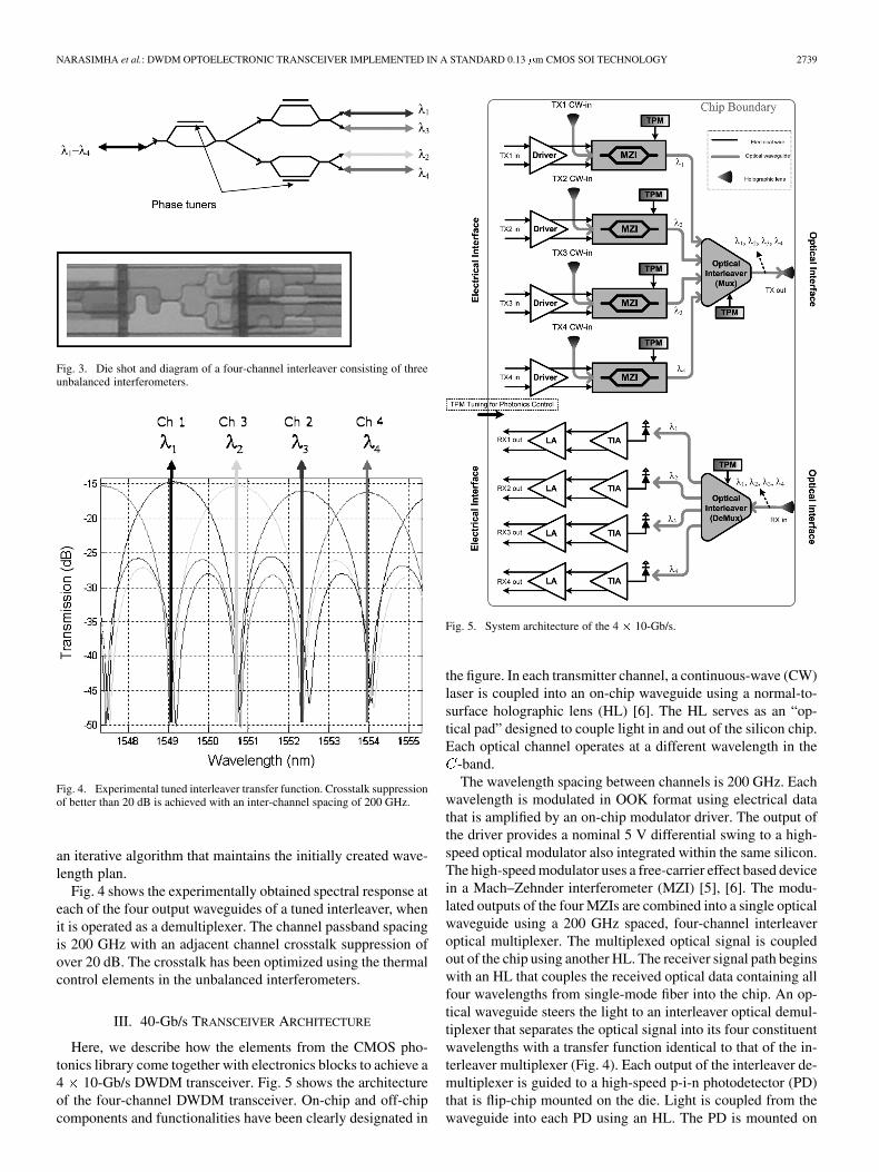
An optical interleaver consists of a series of cascaded, unbal-anced optical interferometers. Such a device achieves a desiredfilter function by multiplying the spectral response of unbal-anced interferometers with different length imbalances. Fig. 2illustrates the way an unbalanced interferometer works. Such adevice creates a periodic spectrally selective transfer functionat its two outputs. Light entering the interferometer is split intotwo arms by an optical directional coupler. The length imbal-ance in the interferometer allows light to accumulate a substan-tial amount of wavelength dependent phase in one arm relativeto the other arm. When the phase accumulated is an integralmultiple of , the two arms interfere in the output directionalcoupler, creating constructive interference in one port and de-structive interference in the other port. When the phase accu-mulated is an odd multiple of , the role of the output ports isreversed. The two outputs are complementary, conserving thenet optical throughput, thus generating an “interleaving” func-tion as illustrated in Fig. 2.
The electric field transfer function of such a structure isobtained by simply multiplying individual directional couplertransfer functions with the transfer function of the waveguidesthat connect them and is given by
(1)

2738 IEEE JOURNAL OF SOLID-STATE CIRCUITS, VOL. 42, NO. 12, DECEMBER 2007
Fig. 2. Functionality of an unbalanced interferometer.
where , , , and are theelectric field vectors as a function of wavelength, correspondingto the optical intensities , , and
, respectively, as indicated in Fig. 2, is the op-tical power excess loss of a directional coupler, is the fieldattenuation coefficient of the optical waveguide per unit length,
is the length of the lower interferometer arm, isthe difference between the upper and lower interferometer armsgiven by , is the effective indexof the optical waveguide as a function of wavelength, andis is the phase induced in the upper or lower interferometer armby a current driven through the phase control element.
It is clear from (1) that the transfer function can be modifiedvia the upper and lower interferometer phase control terms
, allowing us to control the location of the peaks and nullsin the function by applying a suitable current to the phasecontrol elements. This allows for shaping and positioning thenulls and peaks of the transfer function with respect to a desiredwavelength, allowing us to compensate for process variationsand temperature-induced variations in the transfer function of agiven device.
Fig. 2 plots the output optical intensities, andcorresponding to the fields given by (1) for the
shown in the figure. In this case, .Note the complementary interleaving nature of the two outputfunctions.
The periodicity of the nulls seen in the transfer function de-pends on the path-length difference between the two arms of theunbalanced interferometer and is given by
(2)
where is the period of the nulls in the transfer function ingigahertz, is the speed of light in a vacuum expressed in metersper second, is the path-length difference between the twoarms of the unbalanced interferometer in nanometers, and isthe group velocity index of the optical waveguide used in theinterferometer arms.
Unbalanced interferometers of different are cascaded to-gether, multiplying out different transfer functions to generatea desired spectral response. A four-channel interleaver employsthree unbalanced interferometers, as illustrated in the diagramand die shot in Fig. 3. Random variations in the process man-ifest themselves as local variations in the waveguide index, re-sulting in an inability to predict the exact peak of the individualstage transfer functions. Additionally, the imbalance in the in-terferometer makes its transfer function sensitive to temperature(via an effective index change) due to the thermooptic effect insilicon. These variations serve to degrade the overall interleavertransfer function resulting in crosstalk between the wavelengths.Tuning the interferometer using its control elements induces achange in the effective length of the waveguide, thus modifyingone of the terms in (1). To reduce the crosstalk, current isapplied to low-speed TPMs in the upper or lower arms of theindividual interferometers. Tuning the interleaver during chipstartup is simply a matter of adjusting the current through theindividual phase-control elements till the power at the desiredoutput port is maximized for a given wavelength. Since the in-terleaver is designed for an inter-channel spacing of 200 GHz,maximizing one wavelength at a given output port ensures thesuppression of other wavelengths in the DWDM wavelengthplan. In operation, the three interferometers are continuouslytuned by maximizing the output power from each channel using
NARASIMHA et al.: DWDM OPTOELECTRONIC TRANSCEIVER IMPLEMENTED IN A STANDARD 0.13 m CMOS SOI TECHNOLOGY 2739
Fig. 3. Die shot and diagram of a four-channel interleaver consisting of threeunbalanced interferometers.
Fig. 4. Experimental tuned interleaver transfer function. Crosstalk suppressionof better than 20 dB is achieved with an inter-channel spacing of 200 GHz.
an iterative algorithm that maintains the initially created wave-length plan.
Fig. 4 shows the experimentally obtained spectral response ateach of the four output waveguides of a tuned interleaver, whenit is operated as a demultiplexer. The channel passband spacingis 200 GHz with an adjacent channel crosstalk suppression ofover 20 dB. The crosstalk has been optimized using the thermalcontrol elements in the unbalanced interferometers.
III. 40-Gb/s TRANSCEIVER ARCHITECTURE
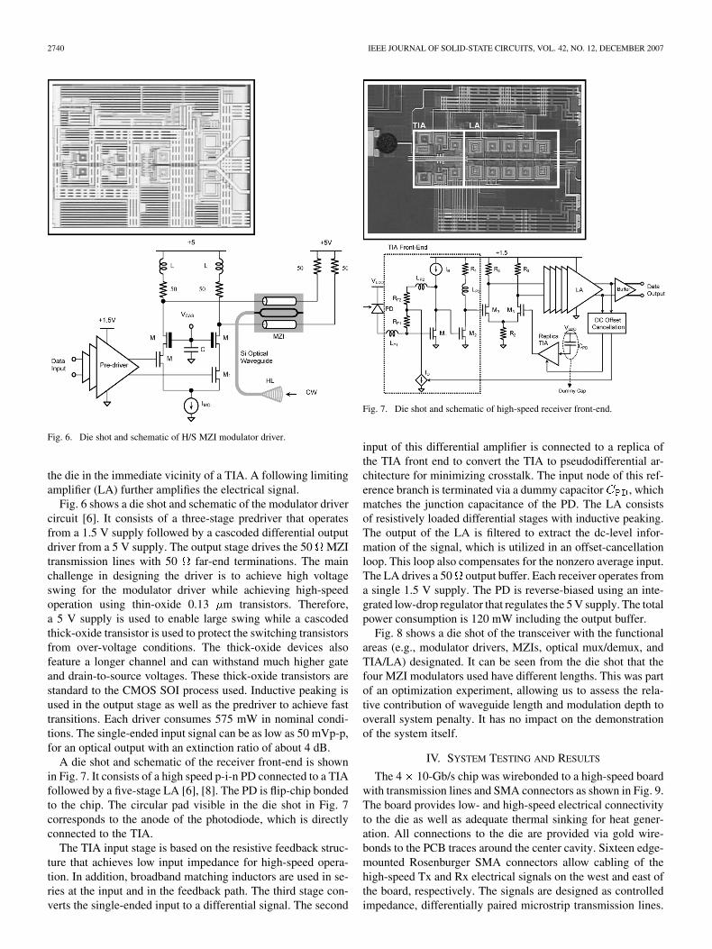
Here, we describe how the elements from the CMOS pho-tonics library come together with electronics blocks to achieve a4 10-Gb/s DWDM transceiver. Fig. 5 shows the architectureof the four-channel DWDM transceiver. On-chip and off-chipcomponents and functionalities have been clearly designated in
Fig. 5. System architecture of the 4 � 10-Gb/s.
the figure. In each transmitter channel, a continuous-wave (CW)laser is coupled into an on-chip waveguide using a normal-to-surface holographic lens (HL) [6]. The HL serves as an “op-tical pad” designed to couple light in and out of the silicon chip.Each optical channel operates at a different wavelength in the
-band.The wavelength spacing between channels is 200 GHz. Each
wavelength is modulated in OOK format using electrical datathat is amplified by an on-chip modulator driver. The output ofthe driver provides a nominal 5 V differential swing to a high-speed optical modulator also integrated within the same silicon.The high-speed modulator uses a free-carrier effect based devicein a Mach–Zehnder interferometer (MZI) [5], [6]. The modu-lated outputs of the four MZIs are combined into a single opticalwaveguide using a 200 GHz spaced, four-channel interleaveroptical multiplexer. The multiplexed optical signal is coupledout of the chip using another HL. The receiver signal path beginswith an HL that couples the received optical data containing allfour wavelengths from single-mode fiber into the chip. An op-tical waveguide steers the light to an interleaver optical demul-tiplexer that separates the optical signal into its four constituentwavelengths with a transfer function identical to that of the in-terleaver multiplexer (Fig. 4). Each output of the interleaver de-multiplexer is guided to a high-speed p-i-n photodetector (PD)that is flip-chip mounted on the die. Light is coupled from thewaveguide into each PD using an HL. The PD is mounted on
2740 IEEE JOURNAL OF SOLID-STATE CIRCUITS, VOL. 42, NO. 12, DECEMBER 2007
Fig. 6. Die shot and schematic of H/S MZI modulator driver.
the die in the immediate vicinity of a TIA. A following limitingamplifier (LA) further amplifies the electrical signal.
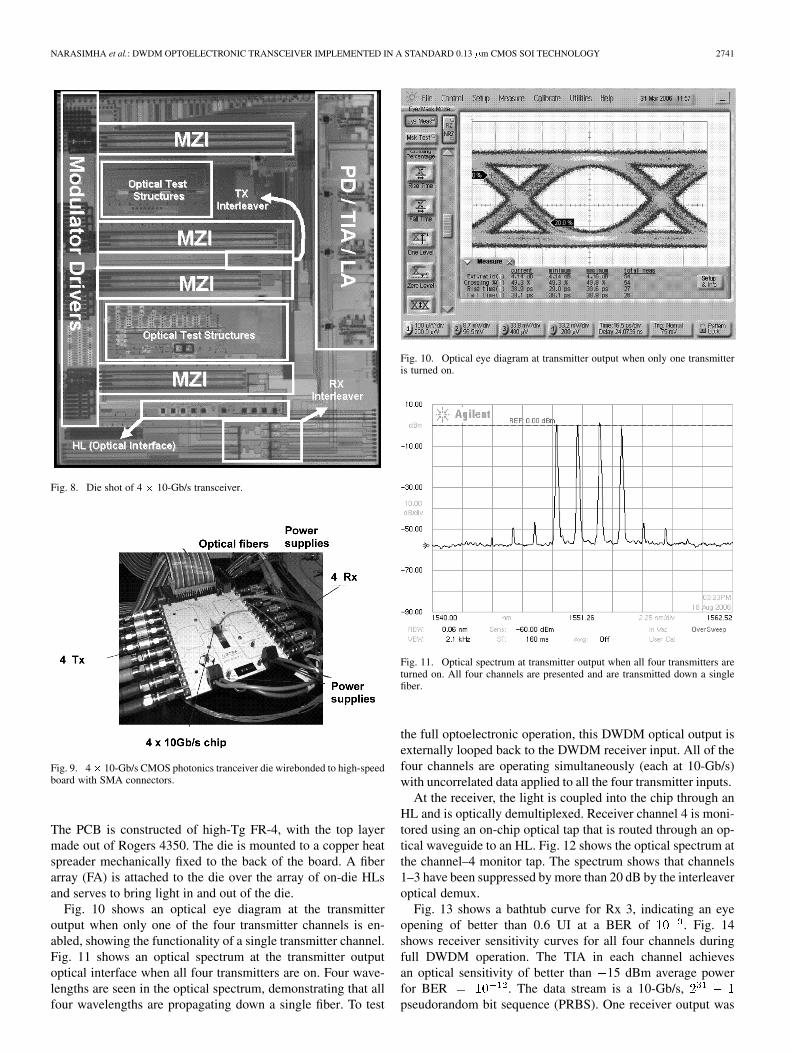
Fig. 6 shows a die shot and schematic of the modulator drivercircuit [6]. It consists of a three-stage predriver that operatesfrom a 1.5 V supply followed by a cascoded differential outputdriver from a 5 V supply. The output stage drives the 50 MZItransmission lines with 50 far-end terminations. The mainchallenge in designing the driver is to achieve high voltageswing for the modulator driver while achieving high-speedoperation using thin-oxide 0.13 m transistors. Therefore,a 5 V supply is used to enable large swing while a cascodedthick-oxide transistor is used to protect the switching transistorsfrom over-voltage conditions. The thick-oxide devices alsofeature a longer channel and can withstand much higher gateand drain-to-source voltages. These thick-oxide transistors arestandard to the CMOS SOI process used. Inductive peaking isused in the output stage as well as the predriver to achieve fasttransitions. Each driver consumes 575 mW in nominal condi-tions. The single-ended input signal can be as low as 50 mVp-p,for an optical output with an extinction ratio of about 4 dB.
A die shot and schematic of the receiver front-end is shownin Fig. 7. It consists of a high speed p-i-n PD connected to a TIAfollowed by a five-stage LA [6], [8]. The PD is flip-chip bondedto the chip. The circular pad visible in the die shot in Fig. 7corresponds to the anode of the photodiode, which is directlyconnected to the TIA.
The TIA input stage is based on the resistive feedback struc-ture that achieves low input impedance for high-speed opera-tion. In addition, broadband matching inductors are used in se-ries at the input and in the feedback path. The third stage con-verts the single-ended input to a differential signal. The second
Fig. 7. Die shot and schematic of high-speed receiver front-end.
input of this differential amplifier is connected to a replica ofthe TIA front end to convert the TIA to pseudodifferential ar-chitecture for minimizing crosstalk. The input node of this ref-erence branch is terminated via a dummy capacitor , whichmatches the junction capacitance of the PD. The LA consistsof resistively loaded differential stages with inductive peaking.The output of the LA is filtered to extract the dc-level infor-mation of the signal, which is utilized in an offset-cancellationloop. This loop also compensates for the nonzero average input.The LA drives a 50 output buffer. Each receiver operates froma single 1.5 V supply. The PD is reverse-biased using an inte-grated low-drop regulator that regulates the 5 V supply. The totalpower consumption is 120 mW including the output buffer.
Fig. 8 shows a die shot of the transceiver with the functionalareas (e.g., modulator drivers, MZIs, optical mux/demux, andTIA/LA) designated. It can be seen from the die shot that thefour MZI modulators used have different lengths. This was partof an optimization experiment, allowing us to assess the rela-tive contribution of waveguide length and modulation depth tooverall system penalty. It has no impact on the demonstrationof the system itself.
IV. SYSTEM TESTING AND RESULTS
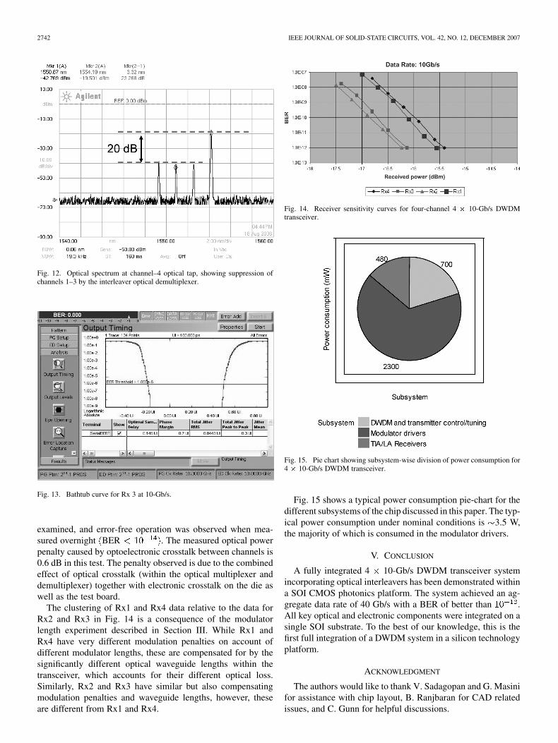
The 4 10-Gb/s chip was wirebonded to a high-speed boardwith transmission lines and SMA connectors as shown in Fig. 9.The board provides low- and high-speed electrical connectivityto the die as well as adequate thermal sinking for heat gener-ation. All connections to the die are provided via gold wire-bonds to the PCB traces around the center cavity. Sixteen edge-mounted Rosenburger SMA connectors allow cabling of thehigh-speed Tx and Rx electrical signals on the west and east ofthe board, respectively. The signals are designed as controlledimpedance, differentially paired microstrip transmission lines.
NARASIMHA et al.: DWDM OPTOELECTRONIC TRANSCEIVER IMPLEMENTED IN A STANDARD 0.13 m CMOS SOI TECHNOLOGY 2741
Fig. 8. Die shot of 4 � 10-Gb/s transceiver.
Fig. 9. 4� 10-Gb/s CMOS photonics tranceiver die wirebonded to high-speedboard with SMA connectors.
The PCB is constructed of high-Tg FR-4, with the top layermade out of Rogers 4350. The die is mounted to a copper heatspreader mechanically fixed to the back of the board. A fiberarray (FA) is attached to the die over the array of on-die HLsand serves to bring light in and out of the die.
Fig. 10 shows an optical eye diagram at the transmitteroutput when only one of the four transmitter channels is en-abled, showing the functionality of a single transmitter channel.Fig. 11 shows an optical spectrum at the transmitter outputoptical interface when all four transmitters are on. Four wave-lengths are seen in the optical spectrum, demonstrating that allfour wavelengths are propagating down a single fiber. To test
Fig. 10. Optical eye diagram at transmitter output when only one transmitteris turned on.
Fig. 11. Optical spectrum at transmitter output when all four transmitters areturned on. All four channels are presented and are transmitted down a singlefiber.
the full optoelectronic operation, this DWDM optical output isexternally looped back to the DWDM receiver input. All of thefour channels are operating simultaneously (each at 10-Gb/s)with uncorrelated data applied to all the four transmitter inputs.
At the receiver, the light is coupled into the chip through anHL and is optically demultiplexed. Receiver channel 4 is moni-tored using an on-chip optical tap that is routed through an op-tical waveguide to an HL. Fig. 12 shows the optical spectrum atthe channel–4 monitor tap. The spectrum shows that channels1–3 have been suppressed by more than 20 dB by the interleaveroptical demux.
Fig. 13 shows a bathtub curve for Rx 3, indicating an eyeopening of better than 0.6 UI at a BER of . Fig. 14shows receiver sensitivity curves for all four channels duringfull DWDM operation. The TIA in each channel achievesan optical sensitivity of better than 15 dBm average powerfor BER . The data stream is a 10-Gb/s,pseudorandom bit sequence (PRBS). One receiver output was
2742 IEEE JOURNAL OF SOLID-STATE CIRCUITS, VOL. 42, NO. 12, DECEMBER 2007
Fig. 12. Optical spectrum at channel–4 optical tap, showing suppression ofchannels 1–3 by the interleaver optical demultiplexer.
Fig. 13. Bathtub curve for Rx 3 at 10-Gb/s.
examined, and error-free operation was observed when mea-sured overnight BER . The measured optical powerpenalty caused by optoelectronic crosstalk between channels is0.6 dB in this test. The penalty observed is due to the combinedeffect of optical crosstalk (within the optical multiplexer anddemultiplexer) together with electronic crosstalk on the die aswell as the test board.
The clustering of Rx1 and Rx4 data relative to the data forRx2 and Rx3 in Fig. 14 is a consequence of the modulatorlength experiment described in Section III. While Rx1 andRx4 have very different modulation penalties on account ofdifferent modulator lengths, these are compensated for by thesignificantly different optical waveguide lengths within thetransceiver, which accounts for their different optical loss.Similarly, Rx2 and Rx3 have similar but also compensatingmodulation penalties and waveguide lengths, however, theseare different from Rx1 and Rx4.
Fig. 14. Receiver sensitivity curves for four-channel 4 � 10-Gb/s DWDMtransceiver.
Fig. 15. Pie chart showing subsystem-wise division of power consumption for4 � 10-Gb/s DWDM transceiver.
Fig. 15 shows a typical power consumption pie-chart for thedifferent subsystems of the chip discussed in this paper. The typ-ical power consumption under nominal conditions is 3.5 W,the majority of which is consumed in the modulator drivers.
V. CONCLUSION
A fully integrated 4 10-Gb/s DWDM transceiver systemincorporating optical interleavers has been demonstrated withina SOI CMOS photonics platform. The system achieved an ag-gregate data rate of 40 Gb/s with a BER of better than .All key optical and electronic components were integrated on asingle SOI substrate. To the best of our knowledge, this is thefirst full integration of a DWDM system in a silicon technologyplatform.
ACKNOWLEDGMENT
The authors would like to thank V. Sadagopan and G. Masinifor assistance with chip layout, B. Ranjbaran for CAD relatedissues, and C. Gunn for helpful discussions.
NARASIMHA et al.: DWDM OPTOELECTRONIC TRANSCEIVER IMPLEMENTED IN A STANDARD 0.13 m CMOS SOI TECHNOLOGY 2743
REFERENCES
[1] J. W. Goodman, F. J. Leonberger, S.-Y. Kung, and R. A. Athale, “Op-tical interconnections for VLSI systems,” Proc. IEEE, vol. 72, no. 7,pp. 850–866, Jul. 1984.
[2] D. A. B. Miller, “Rationale and challenges for optical interconnects toelectronics chips,” Proc. IEEE, vol. 88, no. 6, pp. 728–749, Jun. 2000.
[3] S. Bates and K. Iniewski, “10 GBPS over copper lines—State of the artin VLSI,” in Proc. 5th Int. Workshop Systems-on-Chip for Real-TimeApplications, Jul. 2005, pp. 491–494.
[4] T. Beukema et al., “A 6.4-Gb/s CMOS SerDes core with feed-forwardand decision-feedback equalization,” IEEE J. Solid-State Circuits, vol.40, no. 12, pp. 2633–2645, Dec. 2005.
[5] A. Huang et al., “A 10 Gb/s photonic modulator and WDM MUX/DEMUX integrated with electronics in 0.13-�m SOI CMOS,” in IEEEISSCC Dig. Tech. Papers, 2006, pp. 244–245.
[6] B. Analui, D. Guckenberger, D. Kucharski, and A. Narasimha, “A fullyintegrated 20-Gb/s optoelectronic transceiver implemented in a stan-dard 0.13-�m CMOS SOI technology,” IEEE J. Solid-State Circuits,vol. 41, no. 12, pp. 2945–2955, Dec. 2006.
[7] G. T. Reed and A. P. Knights, Silicon Photonics: An Introduction.New York: Wiley, 2004.
[8] F. Pera and S. P. Voinigescu, “An SOI CMOS, high gain and low noisetransimpedance-limiting amplifier for 10 Gb/s applications,” in Proc.IEEE Radio Frequency Integr. Circuits Symp., Jun. 2006.
Adithyaram Narasimha (S’99–M’04) received theB.S. degree in electrical and electronics engineeringfrom the Birla Institute of Technology and Science,Pilani, India, in 1998, and the Ph.D. degree in elec-trical engineering from the University of California,Los Angeles (UCLA), in 2004.
He is currently a Senior Staff Engineer withLuxtera Inc., Carlsbad, CA, where he is part of theProduct Development Team working on the com-pany’s first high-speed optoelectronic transceiver.Previously, at Luxtera, he worked on porting inte-
grated DWDM device technologies to silicon photonics and on optoelectronictransceiver system and subsystem architectures. While at UCLA, he conductedresearch on photonic transmission systems and diffractive photonic devicesin SOI. Prior to UCLA, he was with Siemens Components Pte. Ltd. (nowInfineon), Singapore, where he worked on DRAMs in the Signal Processing ICGroup.
Dr. Narasimha was a corecipient of the 2006 IEEE Lewis Winner BestPaper Award.
Behnam Analui (S’97–M’05) received the B.S. andM.S. degrees in electronics engineering from theSharif University of Technology, Tehran, Iran, in1998 and 2000, respectively, and the Ph.D. degree inelectrical engineering from the California Instituteof Technology (Caltech), Pasadena, in 2005.
He was with the Mixed-Signal CommunicationsIC Design Group, IBM T. J. Watson Research Center,Yorktown Heights, NY, in 2003, where he developedan eye-opening monitor for 10-Gb/s multimode fiberlinks. He is now a Senior Staff Engineer with Lux-
tera Inc., Carlsbad, CA, as part of the team that is leading the development ofthe world’s first silicon photonics-based transceivers. His technical interests in-clude signal integrity issues in high-speed serial links, jitter, and integrated sil-icon photonics systems.
Dr. Analui was the Silver Medal winner of the National MathematicsOlympiad in 1994. He was the recipient of Caltech’s Atwood Fellowship in2000 and the Analog Devices Outstanding Student Designer Award in 2002.
Yi Liang (SM’02) received the Ph.D. degree in electrical engineering fromNorthern Jiaotong University, Beijing, China, in 1988.
She then taught fiber optics and researched several state and federal govern-ment-funded programs of optical fiber applications at Northern Jiaotong Univer-sity from 1989 to 1994. She joined the Ultrafast Switching Group, Departmentof Electrical Engineering and Computer Science, University of Michigan, Ann
Arbor, in 1995, where she focused on the research of the 100-Gb/s all-opticalswitching program for more than three years. From 2000 to 2004, she was withSorrento Networks Inc., San Diego, CA, where she was involved with the de-velopment of optical switching systems and DWDM optical transport systems.She joined Luxtera Inc., Carlsbad, CA, in October 2004, where she focuses onthe characterization and validation of CMOS photonic devices and systems.
Thomas J. Sleboda received the B.S. degree in ma-terials engineering and the M.S. degree in metallur-gical engineering from the Georgia Institute of Tech-nology, Atlanta, in 1994 and 1996, respectively. Hisgraduate studies were conducted at the Packaging Re-search Center.
He is currently a Senior Staff Engineer with Lux-tera Inc., Carlsbad, CA, where he is involved withpackaging development of products that leverage sil-icon photonics technology. Prior to joining Luxtera,he was with Cameron Health, developing packaging
solutions for subcutaneous implantable defibrillators. Prior to this position, heworked with Big Bear Networks developing packaging technology for OC-768transceiver products. Prior to Big Bear, he was with Motorola (now Freescale)Semiconductor Products Sector, developing packaging solutions for 3G cel-lular applications, PowerPC (IBM Somerset partnership), and the world’s firstflip-chip plastic ball grid array (FC-PBGA) product.
Sherif Abdalla (S’98–M’02) received the B.Sc.degree in electrical engineering and communicationfrom Cairo University, Cairo, Egypt, in 1992, andthe M.S. degree in electrical engineering from theUniversity of Toronto, Toronto, ON, Canada, in2002.
From 2002 to 2005, he was with Snowbush,Toronto, working on multi-Gb/s serial links. Since2005, he has been with Luxtera Inc., Carlsbad, CA,where he is the Director of Engineering responsiblefor electronics IC design activities. Prior to his IC
design career, he has worked on different technologies in robotics, machinevision, and oil-field measurement systems.
Erwin Balmater, photograph and biography not available at the time of publi-cation.
Steffen Gloeckner received the Ph.D. degree inphysics from Friedrich-Schiller-University, Jena,Germany.
He is a Director of Engineering with LuxteraInc., Carlsbad, CA, where he is responsible formanaging the Photonics Components and SystemDesign Group. Prior to Luxtera, he held design andproduct engineering positions with the FraunhoferInstitute for Applied Optics and Precision Engi-neering, Jena, Germany, and OMM, a manufacturerof MEMS-based optical switches.
Drew Guckenberger (S’00–M’05) received theB.A.Sc. degree in systems design engineering fromthe University of Waterloo, Waterloo, ON, Canada,in 2000, and the M.S. and Ph.D. degrees in electricaland computer engineering from Cornell University,Ithaca, NY, in 2003 and 2005, respectively.
He spent the summers of 2002–2004 at IBM’sT. J. Watson Research Center, Yorktown Heights,NY, where he worked mainly on the developmentof high-speed optical receivers and receiver arrays.He has been with Luxtera Inc., Carlsbad, CA, since
2744 IEEE JOURNAL OF SOLID-STATE CIRCUITS, VOL. 42, NO. 12, DECEMBER 2007
2005. His research interests focus mainly on the development of low-powerhigh-performance analog circuits for communication system applications.
Dr. Guckenberger was the recipient of the Cornell IEEE Teaching Assis-tant of the Year Award in 2000-2001 and has been the recipient of an IBMPh.D. Fellowship (2001-2003), a Qualcomm Design Fellowship (2004), and anIntel Ph.D. Fellowship (2004–2005). He also received the 2004 IEEE Bipolar/BiCMOS Circuits and Technology Meeting (BCTM) Best Student Paper Award.
Mark Harrison, photograph and biography not available at the time ofpublication.
Roger G. M. P. Koumans was born in Heerlen,The Netherlands, on January 17, 1971. He receivedthe B.S. and M.S. degrees (cum laude) in electricalengineering from Eindhoven University of Tech-nology, Division of Optical Telecommunications,Eindhoven, The Netherlands, in 1994, and the M.S.and Ph.D. degrees in electrical engineering fromthe California Institute of Technology, Pasadena, in1996 and 2000, respectively. His Ph.D. dissertationfocused on the modeling, characterization, andapplications of mode-locked semiconductor and
fiber lasers as well as on wavelength-division multiplexing, ultrashort pulsemeasurements and pulse shaping, wavelength conversion, fiber Bragg gratings,and nonlinear optics.
In partial fulfillment of his master’s degree from Eindhoven University ofTechnology, he worked for Philips Optoelectronics Centre, Eindhoven, onmode-locked semiconductor lasers. After obtaining the Ph.D. degree, he joinedOrbits Lightwave, Inc., Pasadena, where he concentrated his research effortson the development of ultrastable, low-noise, single-frequency fiber lasers thatnow find application in military, LIDAR, and subterranean applications. In De-cember 2003, he joined Luxtera Inc., Carlsbad, CA. His main research effortsfocus on the modeling, design, and testing of novel CMOS photonic devicesand systems, semiconductor and Raman lasers, electrooptical modulators, andother silicon-on-insulator (SOI) devices. He has been awarded several U.S. andinternational patents for his scientific contributions in his field.
Daniel Kucharski (S’00–M’05) received the B.S.degree in electrical engineering from the RochesterInstitute of Technology, Rochester, NY, in 1998,and the Ph.D. degree in electrical engineering fromCornell University, Ithaca, NY, in 2005.
From 1998 to 2000, he was with IBM Micro-electronics, Burlington, VT, where he worked onASIC library development. He spent the summersof 2001–2004 at the IBM T. J. Watson ResearchCenter, Yorktown Heights, NY, where he workedon parallel optical data links in SiGe and CMOS. In
2005 he joined Luxtera Inc., Carlsbad, CA, where he is currently involved indevelopment of CMOS circuits for silicon photonics applications.
Attila Mekis received the B.S. degree in physicsfrom Yale University, New Haven, CT, and the Ph.D.degree in theoretical condensed matter physics fromthe Massachusetts Institute of Technology (MIT),Cambridge, in 2000,
He is currently a Principal Engineer with LuxteraInc., Carlsbad, CA, where he is currently responsiblefor the development of integrated optoelectroniccomponents. Prior to joining Luxtera in 2004, he waswith Inplane Photonics and Clarendon Photonics,developing integrated optics components for wave-
guide amplifiers and reconfigurable OADMs, respectively. While at MIT, heconducted research on photonic crystal-based optical components and workedas a consultant for Bell Labs designing photonic crystal lasers.
Sina Mirsaidi received the B.S. degree in electricalengineering from Tehran University, Tehran, Iran, in1989, and the M.S. and Ph.D. degrees in electrical en-gineering from École Supérieure d’Électricité (SUP-ELEC), Paris, France, in 1993 and 1997, respectively.
From 1997 to 1998, he was a Research Engi-neer with the University of Toronto, Toronto, ON,Canada, where he pursued his interests in the areasof speech compression, adaptive signal processingfor nonuniformly sampled signals, as well as detec-tion/estimation strategies for wireless receivers. In
1999, he joined Nortel Networks, Ottawa, ON, Canada, as a Member of theTechnical Staff, where he worked on design and development of broadbandwireless access products for residential and commercial applications. From2000 to 2001, he was actively involved in product definition and design ofNortel Networks’ Long Haul (LH) fiber-optic-based DWDM systems. From2001 to 2004, he was a System Architect with Ceyba Inc., Ottawa, where hewas in charge of system design and implementation of large/high-capacityend-to-end core optical network systems. In 2004, he joined Luxtera Inc.,Carlsbad, CA, where he is currently managing the system design and develop-ment of fiber-optic-based high-speed transceivers. During 2001, he was also aSystem Engineering consultant for Cisco Systems.
Dan Song, photograph and biography not available at the time of publication.
Thierry Pinguet received the engineering degreeand the M.S. degree from the Ecole Polytechnique,Palaiseau, France, and the Ph.D. degree in appliedphysics from Stanford University, Stanford, CA.
He is currently a Principal Engineer with LuxteraInc., Carlsbad, CA, where he has since 2002 beenleading the development of the company’s CMOSphotonics technology. While at Stanford, his researchconcentrated on the design, fabrication, and testingof guided-wave and bulk nonlinear optical devices inGaAs for applications ranging from military coun-
termeasures to optical communications. His work has led to numerous break-throughs in photonic design and fabrication techniques, and he is the owner of23 patents.