IEEE TRANSACTIONS ON CIRCUITS AND SYSTEMS—I: REGULAR
13
IEEE TRANSACTIONS ON CIRCUITS AND SYSTEMS—I: REGULAR PAPERS, VOL. 54, NO. 5, MAY 2007 981 A Multichip Pulse-Based Neuromorphic Infrastructure and Its Application to a Model of Orientation Selectivity Elisabetta Chicca, Member, IEEE, Adrian M. Whatley, Patrick Lichtsteiner, Vittorio Dante, Tobias Delbruck, Senior Member, IEEE, Paolo Del Giudice, Rodney J. Douglas, and Giacomo Indiveri, Senior Member, IEEE Abstract—The growing interest in pulse-mode processing by neural networks is encouraging the development of hardware im- plementations of massively parallel networks of integrate-and-fire neurons distributed over multiple chips. Address-event represen- tation (AER) has long been considered a convenient transmission protocol for spike based neuromorphic devices. One missing, long-needed feature of AER-based systems is the ability to acquire data from complex neuromorphic systems and to stimulate them using suitable data. We have implemented a general-purpose solution in the form of a peripheral component interconnect (PCI) board (the PCI-AER board) supported by software. We describe the main characteristics of the PCI-AER board, and of the related supporting software. To show the functionality of the PCI-AER infrastructure we demonstrate a reconfigurable multichip neuro- morphic system for feature selectivity which models orientation tuning properties of cortical neurons. Index Terms—Address event representation (AER), asyn- chronous, cooperative–competitive, neural chips, neural networks, neuromorphic, orientation tuning, peripheral component inter- connect (PCI)-AER, VLSI, winner take all (WTA). I. INTRODUCTION N ETWORKS of integrate-and-fire (I&F) neurons have been shown to exhibit a wide range of useful compu- tational properties, including feature binding, segmentation, pattern recognition, onset detection, input prediction, etc. [1]. Implementing these functionality in VLSI circuits could lead to the construction of efficient hardware systems capable of solving complex sensory processing tasks in real-time. I&F neuron circuits are very well suited for VLSI implementation [2]–[8]. Large VLSI networks of I&F neurons can already be implemented on single chips, using today’s technology. However implementations of pulse-based neural networks on multichip systems offer greater computational power and higher Manuscript received November 22, 2005; revised June 29, 2006, October 9, 2006. This work was supported in part by the EU under Grant ALAVLSI IST-2001-38099, Grant CAVIAR IST-2001-34124, and Grant DAISY (FP6-2005-015803 and in part by the Swiss National Science Foundation unde Grant PMPD2-110298/1. This paper was recommended by Associate Editor G. Cauwenberghs. E. Chicca, A. M. Whatley, P. Lichtsteiner, T. Delbruck, R. J. Douglas, and G. Indiveri are with the Institute of Neuroinformatics (INI), University of Zurich, Zurich CH-8057, Switzerland and the Swiss Federal Institute of Technology (ETHZ), Zurich CH-8092, Switzerland. V. Dante is with the Italian National Institute of Health, 00161 Rome, Italy. P. Del Giudice is with the Italian National Institute of Health, 00161 Rome, Italy, and also with the National Institute of Nuclear Physics (INFN), 00185 Rome, Italy. Digital Object Identifier 10.1109/TCSI.2007.893509 flexibility than single-chip systems. As inter-chip connectivity is limited by the small number of input-output connections available with standard chip packaging technologies, it is necessary to adopt time-multiplexing schemes for constructing large multichip networks. A. Address Event Representation (AER) In recent years, we have witnessed the emergence of new asynchronous communication protocols that allow aVLSI neu- rons to transmit their activity across chips using pulse-frequency modulated signals (in the form of events, or spikes). One of the most common asynchronous communication protocols used in these types of systems is the so-called address-event represen- tation (AER) communication protocol [9]–[12]. In this repre- sentation, input and output signals are real-time digital events that carry analog information in their temporal relationships (inter-spike intervals). Each event is represented by a binary word encoding the address of the sending node. The activity of biological neurons is sparse in time, with typ- ical firing rates ranging from a few per second to a few hundred per second. The speed of digital buses (tens of megahertz) al- lows the outputs of many VLSI neurons firing at these biologi- cally typical rates to be multiplexed over one AE bus. To further reduce the bandwidth required on the AE bus, local connectivity can be hardwired on-chip [4], [8]. To handle cases in which mul- tiple sending nodes attempt to transmit their addresses at exactly the same time (event collisions) on-chip arbitration schemes can be used [9], [13]–[15]. Chips that communicate using the AER communication pro- tocol can be divided into senders with AER output only (e.g., silicon retinas [16], [17], or silicon cochleas [18]), receivers with AER input only [19], and transceiver chips, which are both senders and receivers [2], [7], [8]. Systems containing more than one AER sender chips can be assembled using off-chip arbitration. One of the earliest multichip systems using the AER commu- nication protocol, a silicon model of stereoscopic vision, was implemented by Misha Mahowald [9]. The system, consisting of three silicon chips interconnected with asynchronous digital buses, was able to extract, in real-time, depth information from visual stimuli detected by two silicon retinas. At that time and since, logic analyzers were and are often used to monitor AE buses. While still useful for debugging problems with AE pro- tocol communication they suffer from several disadvantages for 1549-8328/$25.00 © 2007 IEEE
Transcript of IEEE TRANSACTIONS ON CIRCUITS AND SYSTEMS—I: REGULAR

IEEE TRANSACTIONS ON CIRCUITS AND SYSTEMS—I: REGULAR PAPERS, VOL. 54, NO. 5, MAY 2007 981
A Multichip Pulse-Based NeuromorphicInfrastructure and Its Application to a Model
of Orientation SelectivityElisabetta Chicca, Member, IEEE, Adrian M. Whatley, Patrick Lichtsteiner, Vittorio Dante,
Tobias Delbruck, Senior Member, IEEE, Paolo Del Giudice, Rodney J. Douglas, andGiacomo Indiveri, Senior Member, IEEE
Abstract—The growing interest in pulse-mode processing byneural networks is encouraging the development of hardware im-plementations of massively parallel networks of integrate-and-fireneurons distributed over multiple chips. Address-event represen-tation (AER) has long been considered a convenient transmissionprotocol for spike based neuromorphic devices. One missing,long-needed feature of AER-based systems is the ability to acquiredata from complex neuromorphic systems and to stimulate themusing suitable data. We have implemented a general-purposesolution in the form of a peripheral component interconnect (PCI)board (the PCI-AER board) supported by software. We describethe main characteristics of the PCI-AER board, and of the relatedsupporting software. To show the functionality of the PCI-AERinfrastructure we demonstrate a reconfigurable multichip neuro-morphic system for feature selectivity which models orientationtuning properties of cortical neurons.
Index Terms—Address event representation (AER), asyn-chronous, cooperative–competitive, neural chips, neural networks,neuromorphic, orientation tuning, peripheral component inter-connect (PCI)-AER, VLSI, winner take all (WTA).
I. INTRODUCTION
NETWORKS of integrate-and-fire (I&F) neurons havebeen shown to exhibit a wide range of useful compu-
tational properties, including feature binding, segmentation,pattern recognition, onset detection, input prediction, etc. [1].Implementing these functionality in VLSI circuits could leadto the construction of efficient hardware systems capable ofsolving complex sensory processing tasks in real-time. I&Fneuron circuits are very well suited for VLSI implementation[2]–[8]. Large VLSI networks of I&F neurons can alreadybe implemented on single chips, using today’s technology.However implementations of pulse-based neural networks onmultichip systems offer greater computational power and higher
Manuscript received November 22, 2005; revised June 29, 2006, October9, 2006. This work was supported in part by the EU under Grant ALAVLSIIST-2001-38099, Grant CAVIAR IST-2001-34124, and Grant DAISY(FP6-2005-015803 and in part by the Swiss National Science Foundation undeGrant PMPD2-110298/1. This paper was recommended by Associate EditorG. Cauwenberghs.
E. Chicca, A. M. Whatley, P. Lichtsteiner, T. Delbruck, R. J. Douglas,and G. Indiveri are with the Institute of Neuroinformatics (INI), Universityof Zurich, Zurich CH-8057, Switzerland and the Swiss Federal Institute ofTechnology (ETHZ), Zurich CH-8092, Switzerland.
V. Dante is with the Italian National Institute of Health, 00161 Rome, Italy.P. Del Giudice is with the Italian National Institute of Health, 00161 Rome,
Italy, and also with the National Institute of Nuclear Physics (INFN), 00185Rome, Italy.
Digital Object Identifier 10.1109/TCSI.2007.893509
flexibility than single-chip systems. As inter-chip connectivityis limited by the small number of input-output connectionsavailable with standard chip packaging technologies, it isnecessary to adopt time-multiplexing schemes for constructinglarge multichip networks.
A. Address Event Representation (AER)
In recent years, we have witnessed the emergence of newasynchronous communication protocols that allow aVLSI neu-rons to transmit their activity across chips using pulse-frequencymodulated signals (in the form of events, or spikes). One of themost common asynchronous communication protocols used inthese types of systems is the so-called address-event represen-tation (AER) communication protocol [9]–[12]. In this repre-sentation, input and output signals are real-time digital eventsthat carry analog information in their temporal relationships(inter-spike intervals). Each event is represented by a binaryword encoding the address of the sending node.
The activity of biological neurons is sparse in time, with typ-ical firing rates ranging from a few per second to a few hundredper second. The speed of digital buses (tens of megahertz) al-lows the outputs of many VLSI neurons firing at these biologi-cally typical rates to be multiplexed over one AE bus. To furtherreduce the bandwidth required on the AE bus, local connectivitycan be hardwired on-chip [4], [8]. To handle cases in which mul-tiple sending nodes attempt to transmit their addresses at exactlythe same time (event collisions) on-chip arbitration schemes canbe used [9], [13]–[15].
Chips that communicate using the AER communication pro-tocol can be divided into senders with AER output only (e.g.,silicon retinas [16], [17], or silicon cochleas [18]), receiverswith AER input only [19], and transceiver chips, which are bothsenders and receivers [2], [7], [8]. Systems containing morethan one AER sender chips can be assembled using off-chiparbitration.
One of the earliest multichip systems using the AER commu-nication protocol, a silicon model of stereoscopic vision, wasimplemented by Misha Mahowald [9]. The system, consistingof three silicon chips interconnected with asynchronous digitalbuses, was able to extract, in real-time, depth information fromvisual stimuli detected by two silicon retinas. At that time andsince, logic analyzers were and are often used to monitor AEbuses. While still useful for debugging problems with AE pro-tocol communication they suffer from several disadvantages for
1549-8328/$25.00 © 2007 IEEE

982 IEEE TRANSACTIONS ON CIRCUITS AND SYSTEMS—I: REGULAR PAPERS, VOL. 54, NO. 5, MAY 2007
monitoring purposes. Good logic analyzers are typically bulkyand heavy and therefore not very portable, and too expensiveto equip every researchers’ bench with one. They also do notusually permit on-line real-time monitoring, since data cannotbe downloaded at the same time that it is being acquired intoacquisition memory. This makes logic analyzers unsuitable forexperiments in which it is desired to incorporate conventionalsoftware-based algorithms into the processing loop, e.g., forcertain on-line learning experiments. General purpose data ac-quisition (digital I/O) boards are also not ideal, since most in-expensive boards are not designed for use with asynchronousbuses and each individual event handshake must therefore behandled by software which makes such boards very slow. Onthe AE generation side, the counterpart of the logic analyzeris the pattern generator. These are also not designed with asyn-chronous buses in mind and cannot wait for a handshake to com-plete but can only emit a fixed programmed pattern. Like logicanalyzers, pattern generators can also not take part in on-linesoftware-in-the-loop experiments and are also very expensive.The joint consideration of the needs for AE input and outputsuggests that a single special-purpose device, natively suitedto asynchronous communication, would provide a more conve-nient, cheaper solution.
B. AER Communication Infrastructures
Infrastructures for constructing multichip pulse-based neuro-morphic systems based on AER have been further developed byseveral researchers [10], [13], [20]–[23]. A wide range of exam-ples of multichip AER systems have been presented in the past.These examples have used AER infrastructures that range fromvery bulky and highly complex general purpose solutions [19],[20], [24], to custom solutions in the form of dedicated printedcircuit boards (PCBs) with microcontrollers and/or look-up ta-bles [6], [25], [26]. In addition, a new set of general purposeAER boards with USB and USB2 interfaces have been recentlyproposed [23], [27], [28]. These boards represent a good com-promise between general-purpose functionality, and compact-ness. However, as they are typically placed between AER chipsin the signal processing path, they often do not have access tothe address events of all chips present in the system. Further-more each individual board has often a limited set of function-alities (e.g., to monitor AEs from a sender, to generate and sendsynthetic AEs to a receiver, to merge AEs from two senders intoa receiver input, to map AEs from one address space to another,etc.), or require reprogramming at the field-programmable gatearray (FPGA)/VHDL level in order to assume one of these par-ticular functions. In this paper, we present a general-purpose so-lution in the form of a peripheral component interconnect (PCI)board (the PCI-AER board) that has all of these functionalities,with the possibility of connecting up to four senders with up tofour receivers, that has access to the global AER address spaceused by the system, and that has a well-defined software inter-face. The approach of using one single PCI-AER board ratherthan many smaller USB-AER boards has the disadvantages ofrequiring a PC workstation to be present, even when only map-ping is required, and limiting to some extent the overall sizeof the AER system that can be constructed. But it has the ad-vantage of allowing convenient and rapid prototyping (e.g., by
stimulating, monitoring and/or experimenting with different ad-dress-space mappings), and of allowing seamless integration ofsoftware algorithms [29] (e.g., that implement learning or thatchange the network topology based on the system’s activity).The PCI-AER board is therefore an ideal tool for developingAER neuromorphic models of biological sensors and neocor-tical processing structures. Specifically, we propose to use theboard to study a computational module based on a network ofspiking neurons with cooperative-competitive interactions.
C. Computational System Overview
We are ultimately interested in developing neuromorphicsystems that reproduce some characteristics of neocorticalprocessing modules. Despite significant differences in func-tion across the various cortical areas, the pattern of neuronalconnections within each area is remarkably similar [30]. Thisregular structure suggests that the cortex may use a commoncore processing circuit, or canonical microcircuit, that canbe tuned to perform specific tasks and used in a modularfashion for implementing different functionalities [30], [31].The canonical microcircuit, and its later extensions, emphasizethe role of first order recurrent connections between corticalneurons. These recurrent connections between neurons supportsoft winner-take-all (WTA) mechanisms, in which networksof neurons participate collectively in the generation of anappropriate interpretation of their input.
The computational abilities arising from soft WTA mecha-nisms are especially useful for feature extraction and patternclassification problems. In the second half of this paper, wedescribe an application example comprising an AE temporallydifferentiating vision sensor interfaced to a VLSI device witha cooperative-competitive network of spiking neurons via thePCI-AER board. We apply this AER-based vision system to theimplementation and comparison of two models of orientationselectivity. The models of mechanisms responsible for orien-tation selectivity have been controversial since its discoveryby Hubel and Wiesel [32]. Originally it was believed that theprimary origin of the orientation selectivity of simple cellswas due to feedforward convergence of thalamic input (feed-forward model). Subsequent experimental studies suggestedthat this contribution alone is insufficient to account for allproperties of orientation tuning observed in the visual cortex[33]–[35], leading to the proposal for the involvement of re-current intracortical excitation and inhibition (feedback model)in orientation selectivity. The origin of orientation selectivityin primary visual cortex has been extensively studied as ameans to understand cortical circuitry and cortical computation[34], [36]–[39], and several hardware models of orientationselectivity have been proposed in the past and fabricated withmonolithic [40]–[42] or multichip configurations [4], [7],[43]–[47]. An advantage of multichip configurations is thatthe computational stage is decoupled from the sensing stage.In this way the orientation selectivity computational devicescan be designed to be modular and expandable. Within themultichip configuration approaches there are two main streams:[4], [43], [45] and [46] implement specific architectures withlocal or hardwired connectivity for processing signals obtainedfrom vision sensors, while [7] and [47] propose using general
CHICCA et al.: MULTI-CHIP PULSE-BASED NEUROMORPHIC INFRASTRUCTURE 983
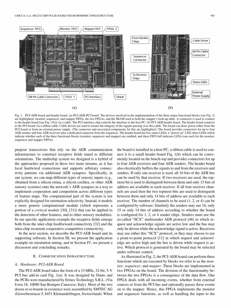
Fig. 1. PCI-AER board and header board. (a) PCI-AER PCI board. The devices involved in the implementation of the three major functional blocks (see Fig. 2)are highlighted: monitor, sequencer, and mapper FIFOs, the two FPGAs, and the SRAM used to hold the mapper’s look-up table. A connector is used to connectto the header board [see Fig. (1b)] via a cable. The PCI interface chip controls the interface to the host PC. (b) PCI-AER header board. The header board connectsto the PCI board via a ribbon cable. Cable drivers are used to ensure the integrity of the signals passing over this cable. The board can draw power either from thePCI board or from an external power supply. (The connector and associated components for this are highlighted.) The board provides connectors for up to fourAER senders and four AER receivers plus a dedicated connector from the sequencer. The header board has five status LEDs: a “power on” LED, three LEDs whichindicate whether each of the three functional blocks (monitor, sequencer and mapper) are enabled, and three FIFO full indicator LEDs (one each for the monitor,sequencer and mapper FIFOs).
purpose transceivers that rely on the AER communicationinfrastructure to construct receptive fields tuned to differentorientations. The multichip system we designed is a hybrid ofthe approaches proposed in these two main streams, as it haslocal hardwired connections and supports arbitrary connec-tivity patterns via additional AER synapses. Specifically, inour system, we can map different types of sensory inputs (e.g.,obtained from a silicon retina, a silicon cochlea, or other AERsensory systems) onto the network’s AER synapses in a way toimplement cooperation and competition across different typesof feature maps. The computational part of the system is notexplicitly designed for orientation selectivity. Instead, it modelsa more generic computational module (which represents aportion of a cortical module [30], [31]) that can be applied tothe detection of other features, and to other sensory modalities.In our specific application example the receptive fields emergeboth from the inter-chip feedforward connectivity [32] and theintra-chip recurrent cooperative-competitive connectivity.
In the next section, we describe the PCI-AER board and itssupporting software. In Section III, we present the applicationexample on orientation tuning, and in Section IV, we present adiscussion and concluding remarks.
II. COMMUNICATION INFRASTRUCTURE
A. Hardware: PCI-AER Board
The PCI-AER board takes the form of a 33 MHz, 32-bit, 5-VPCI bus add-in card Fig. 1(a). It was designed by Dante andthe PCBs were manufactured by Ermes Technology S.R.L. (ViaIvrea 18, 10080 San Benigno Canavese, Italy). Most of the twodozen or so boards in existence were assembled by SMTEC AG(Gewerbestrasse 5, 8451 Kleinandelfingen, Switzerland). When
the board is installed in a host PC, a ribbon cable is used to con-nect it to a small header board Fig. 1(b) which can be conve-niently located on the bench-top and provides connectors for upto four AER receivers and four AER senders. The header boardalso electrically buffers the signals to and from the receivers andsenders. If only one receiver is used, all 16 bits of the AER buscan be used by that receiver. If two receivers are used, the top-most bit is used to distinguish between them and only 15 bits ofaddress are available to each receiver. If all four receiver chan-nels are used then the two topmost bits are used to distinguishbetween them and only 14 bits of address are available to eachreceiver. The number of channels to be used (1, 2, or 4) can beconfigured by software. Similarly the senders may use 16, only15 or only 14 bits of address according to whether the boardis configured for 1, 2, or 4 sender chips. Senders must use theso-called “SCX” multisender AER protocol [48] in which re-quest and acknowledge signals are active low and the bus mayonly be driven while the acknowledge signal is active. Receiversmay use either this “SCX” protocol, or they may choose to usea point-to-point protocol [11] in which request and acknowl-edge are active high and the bus is driven while request is ac-tive. Which protocol is generated by the board may be selectedunder software control.
As illustrated in Fig. 2, the PCI-AER board can perform threefunctions which are executed by blocks we refer to as the mon-itor, sequencer, and mapper. These blocks are implemented intwo FPGAs on the board. The division of the functionality be-tween the two FPGAs is a consequence of the data flow. OneFPGA deals with all incoming events, whether from externalsources or from the PCI bus and optionally passes these eventson to the mapper. Hence, this FPGA implements the monitorand sequencer functions, as well as handling the input to the

984 IEEE TRANSACTIONS ON CIRCUITS AND SYSTEMS—I: REGULAR PAPERS, VOL. 54, NO. 5, MAY 2007
Fig. 2. Block diagram of the PCI-AER interface board showing its three major functional blocks, i.e., the MONITOR, the SEQUENCER, and the mapper (dividedinto MAPPER-IN and MAPPER-OUT). These (and other blocks) are implemented in two FPGAs. Also shown are the FIFOs, the interface from the PCI bus tothe local bus provided by an AMCC S5920 chip [50], the SRAM used to hold the mapper’s look-up table, and the interconnecting buses.
mapper. The other FPGA performs the mapper function proper(including managing the interface to the mapper’s SRAM) andmanages communication with the AER receivers.
The monitor can capture and timestamp events coming fromthe attached AER senders via an arbiter1 and makes those eventsavailable to the PC for storage or further on-line processing. Atimer is implemented in one of the FPGAs, and when an in-coming AE is read, a timestamp is stored along with the addressin a first-in first-out (FIFO) memory. This FIFO decouples themanagement of the incoming AEs from read operations on thePCI bus, the bandwidth of which must be shared with other pe-ripherals in the PC such as the network card. The FIFOs fittedto the current boards are all 8-KWords deep (and 18-bit wide)and since the addresses occupy one word and the timestampstwo words each, this is sufficient to hold 2730 complete events.2
Interrupts to the host PC can be generated when the FIFO be-comes half-full and/or full, and in the ideal case, the driver willread time stamped AEs from the monitor FIFO whenever thehost CPU receives a FIFO half-full interrupt, at a rate sufficientthat the FIFO never fills or overruns, given the rate of incomingAEs. If the CPU fails to empty the FIFO at a sufficient rate, theFIFO will fill up, the FIFO full light-emitting diode (LED) onthe header board will light, and a FIFO full interrupt will begenerated. At this point, incoming events will be lost until suchtime as the CPU can once again read from the FIFO. In the ap-plication example we present in Section III the monitor is usedto record the activity of a sender and a transceiver chip.
1The arbiter is a binary-tree arbiter in which each binary cell is a prioritybased arbiter.
2The monitor can also be run without storing timestamps, in which case theFIFO can hold up to 8 K event addresses.
The sequencer allows events originated by the host PC to besent out to the attached AER receivers. These events may forexample represent a pre-computed, buffered stimulus pattern,but they might also be the result of a real-time computation.This allows for instance software simulations of VLSI devicesto provide input to real VLSI hardware while the former VLSIdevices are still under development. As soon as the real deviceis available, the software simulation can be seamlessly replaced.Like the monitor, the sequencer is decoupled from the PCI bususing an 8-KWord FIFO. The host writes a sequence of wordsrepresenting addresses and time delays to the sequencer FIFO.The sequencer then reads these words one at a time from theFIFO and either emits an AE or waits the indicated number ofmicroseconds. Since addresses and time delays are representedin the sequencer by one word each, and a stream of AEs usuallyconsists of alternating addresses and time delays representinginter-spike intervals, the 8-KWord FIFO can typically hold upto 4096 events. FIFO half empty interrupts can be generated tosignal the CPU to supply further data to the sequencer. If theCPU fails to supply data to the sequencer at a rate sufficient toprevent the sequencer FIFO becoming empty, this may indicatea failure of the system to generate the desired sequence of eventswith the desired timing. In this case a sequencer FIFO emptyinterrupt is raised to signal the underrun. The address eventsgenerated by the sequencer pass through the mapper and cantherefore be transmitted on any of the four output channels.
The mapper implements programmable inter-chip synapticconnectivity. It maps incoming AEs from attached AERsenders and/or the sequencer to one or more outgoing ad-dresses for transmission to the attached AER receivers. It canoperate in pass-through, one-to-one, or one-to-many modes. In

CHICCA et al.: MULTI-CHIP PULSE-BASED NEUROMORPHIC INFRASTRUCTURE 985
pass-through mode, the outgoing addresses are the same as theincoming addresses. In one-to-one mode, each incoming ad-dress is mapped to one outgoing address by using the incomingaddresses as the index into a look-up table stored in on-boardSRAM. This look-up table then holds the corresponding targetoutput addresses. In one-to-many mode, each incoming addressmay be mapped to one or more outgoing addresses. This isachieved by using the contents of the look-up table as pointersto lists of output addresses, also stored in the 2 MWords of onboard SRAM.3 The mapper too has a FIFO which decouplesthe asynchronous reception of the incoming AEs from thegeneration of outgoing AEs. Should this FIFO become full,it is possible that events will be lost, and this eventuality canbe signaled to the CPU by means of an interrupt. The mapper,once it has been configured and the look-up table filled withthe required mappings, operates entirely independently of thehost CPU, since all of the necessary operations, including tablelook-up are performed by one of the FPGAs. To implement themultichip system described in Section III we used the mapperin one-to-many mode.
A detailed description of the hardware (the Hardware UserManual) is available at [49].
B. Supporting Software
To enable the functionality of the board to be accessed robustlyand conveniently, we have provided a Linux device driver and,on top of this, a C library. Both are fully documented and thisdocumentation is available together with the source code at [49].The open-source driver provides full integration of the PCI-AERboard under Linux following the Unix “everything-is-a-file”model. This allows AE data streams to be accessed using stan-dard Unix read and write calls and supports the use of standardshell redirection and command-line tools. The driver providesseparate logical devices for each of the major functional blocksof the board: mapper; monitor; and sequencer, and supportsmultiple boards. It ensures that the AE data streams remaincoherent by serializing accesses from multiple programs runningsimultaneously. It also forces word-multiple sized access toprevent corruption of the data streams due to misalignment.While read and write calls are used to read and write the AE datastreams from and to the board’s FIFOs, IOCTL (input/outputcontrol) calls are provided to set and get configuration states,and user programs are prevented from putting the board into aninconsistent state. The driver also manages the mapper look-uptable memory to relieve users of the task of performing thenecessary but onerous and error-prone table indexing and pointerarithmetic and so prevents the mapping table from becomingcorrupted. Statistics (number of words read or written, numberof interrupts, number of FIFO overruns or underruns etc.) arealso maintained by the driver for each logical device and madeavailable to user programs.
The library consists mainly of thin, fast wrapper functionsaround the driver open, close, read, write, flush and ioctl calls.Functions are also provided to convert from the PCI-AER hard-ware-specific format to a generic inter-spike interval/AE formatfor reading, and vice versa for writing. The conversion function
3In order to send the same address to more than one output channel, the ap-propriate target addresses must be listed serially in the output address lists.
for reading also attempts recovery when data are received outof order because of monitor FIFO overruns or other (hardware)errors.
C. Performance
The performance of the PCI-AER hardware and driver mustbe considered together since the board is unusable without adriver. Once the board has been initialised and configured, anddesired mappings established in the mapper, mapping continuesto operate without intervention from the driver, but a driveris necessary to perform those initialization and configurationsteps, and to read and change mappings later, if so desired. Forthe sequencer, the driver can be used to fill the 4 K-events FIFOand may play no role until the FIFO empties. However it is notpossible to know that the FIFO has emptied without using thedriver, and such a one-shot, 4 K-events-only mode of use is notvery interesting for many applications in which it is desirable tostimulate AER devices continuously. Similarly, events can becollected in the monitor until its FIFO fills up, but they cannotbe read without the driver, nor again is it usually very useful toconstrain data capture to 2 2/3 K events.
Some of the various aspects of the performance are highlydependent on the type of PC in which the board is installed andon which the driver is running, and on the version and config-uration of the Linux kernel in use. Nonetheless the driver is in-strumented for measuring the throughput of the monitor and se-quencer and measurements have been performed using version2.30 of the driver on a 1-GHz, 512-MB, AMD Athlon basedmachine running a SuSE 9.1 Linux distribution with kernel ver-sion 2.6.5. The PCI-AER board FPGA revisions used were 4202(FPGA1) and 4203 (FPGA2). In order to eliminate as many out-side influences as possible and obtain reproducible results, mea-surements were made with no graphical display system and nonetwork stack running. The results of these measurements areshown in Table I. Data for the monitor was obtained by con-necting one monitor input channel to a circuit which producesAE requests at a rate determined by a function generator input,while a test program runs a loop which does nothing but readfrom the driver into a static buffer. The AE rate was then grad-ually increased until FIFO overruns began to occur. The se-quencer data was obtained by connecting together the AE re-quest output and acknowledge input pins on one of the receiverchip connectors on the header board, thus providing the fastestpossible acknowledgement of a request, and running a test pro-gram which configured the board for single channel output withthe mapper in pass-through mode, and which then continuouslywrites the contents of a pre-prepared buffer to the driver. Theinter-spike intervals were specified to be 0 s. The test softwareis available, along with the driver, at [49]. Minimum cycle timeswere measured by observing the request and acknowledge sig-nals at the header board using an oscilloscope. Performance dataobtained when using a more sophisticated software frameworkon top of a slightly earlier version of the driver on a differentmachine were presented in [29].
The limiting factors are various. The sequencer maximumsustainable rate lies in the region between using inter-spike in-tervals of 1 s and inter-spike intervals of 0 s, but since thebest available resolution of the timer controlling the emission of

986 IEEE TRANSACTIONS ON CIRCUITS AND SYSTEMS—I: REGULAR PAPERS, VOL. 54, NO. 5, MAY 2007
TABLE IPCI-AER BOARD AND DRIVER PERFORMANCE DATA
events from the sequencer is 1 s, the timer resolution representsthe limiting factor here. Were the resolution of the timer better,then the data transfer rate would become the limiting factor. Themonitor maximum sustainable rate is determined principally bythe speed at which the AE stream can be read from the boardover the PCI bus and buffered in the PC’s memory. Due to thelack of support for direct memory access (DMA) in the currentdesign, this in turn depends on many factors—CPU speed, cachesize and organization, PCI bus chipset, Linux kernel version etc.
The present board is unable to perform DMA to shift AEdata across the PCI bus because the AMCC S5920 PCI inter-face chip [50] used does not support it, but later generations ofhardware should certainly use DMA, not only to achieve greaterthroughput across the PCI bus, but also to offload the CPU,see for example [51]. Alternatively, with the present board, usemight in future be made of the forthcoming Intel I/O Acceler-ation Technology (I/OAT)4 in which the CPU includes a DMAsubsystem.
Minimum AE cycle times on both the inputs from sendersand on the outputs to receivers depend only on the frequency ofthe clock on the board (20 MHz on the present board) and therequirement to remain within the AER protocol specifications.They do not depend on the number of channels in use, althoughthe latency before acknowledging a request on one arbiter inputchannel may of course be influenced by the presence of eventson other channels if other input channels are in use.
Since the limiting factors are principally on the PC side andnot on the AER side, it is clear that the overall bandwidth avail-able for say monitoring remains constant irrespective of thenumber of channels in use, and that therefore if multiple chan-nels are being monitored, they must share the available band-width. Note however that when not monitoring or sequencing,the bandwidth available on the PCI bus plays no role in the map-ping performance, since the data-path is then from FPGA1 toMapper FIFO to FPGA2 and does not even involve the LocalBus on the board (refer again to Fig. 2).
The throughput of the mapper depends on whether it is beingoperated in pass-through, one-to-one or one-to-many modes,and in the latter case, on the length of the target address listsbeing used. In measuring the sequencer rates given in Table I,the mapper is being used in pass-through mode, thus it is clearthat at least in this mode it can sustain rates of .This would allow neurons to be actively firing at a rate of100 Hz. Assuming no more than 10% of neurons are active atone time, a network of the order of neurons could be sup-ported by one PCI-AER card, but address space considerations
4http://www.intel.com/technology/ioacceleration/.
Fig. 3. AER orientation selectivity system setup. The PCI-AER board routesoutput events of the TMPDIFF chip in response to visual stimuli to the IFWTAchip and monitors the activity of both chips. The PC controls the LCD screenfor stimulus presentation, the PCI-AER board and the DAC board.
restrict us to supporting a maximum of 65536 neurons on thesender side and a maximum of 65536 synapses on the receiverside. If the network produces more spikes than can be processedby the mapper in real-time, then when the mapper FIFO fills,spikes will eventually be lost, but this will have no influence onthe AE protocol cycle times observed on the sender side.
Although the driver supports the use of more than one PCI-AER board in one PC, the user inevitably remains limited bythe characteristics of that host PC and in particular the band-width available for monitoring and/or sequencing within thehost system must then be shared between all of the boards whichare fitted to that system. However as noted above, when boardsare only being used for mapping, there is no impact on the host,so several boards fitted to the same PC might easily be used formapping in larger AE systems while for instance only one boardat a time performs a monitoring function. AEs do not need to berouted from one PCI-AER board to another via the PC but ratherone of the output channels of one board could be connected toone of the input channels of another board, or perhaps to theinput of a transceiver chip the output of which goes to the inputof another board.
III. APPLICATION EXAMPLE: ORIENTATION SELECTIVITY
USING A SILICON RETINA AND A WTA NETWORK
A. Orientation Selectivity System Components
The orientation selectivity system consists of two neuromor-phic aVLSI AER chips, a PCI-AER board and supporting hard-ware (see Fig. 3). The neuromorphic chips are an AE tempo-rally differentiating (TMPDIFF) vision sensor chip [52] and arecurrent competitive network of I&F neurons and short-termdynamic synapses (IFWTA chip) [53].
The AEs generated by the TMPDIFF chip and sent to theWTA chip are routed by the PCI-AER board mapper. ThePCI-AER board monitor is used to read all AEs (generated bythe two chips), timestamp them and log them on the host PC(see Fig. 3).
CHICCA et al.: MULTI-CHIP PULSE-BASED NEUROMORPHIC INFRASTRUCTURE 987
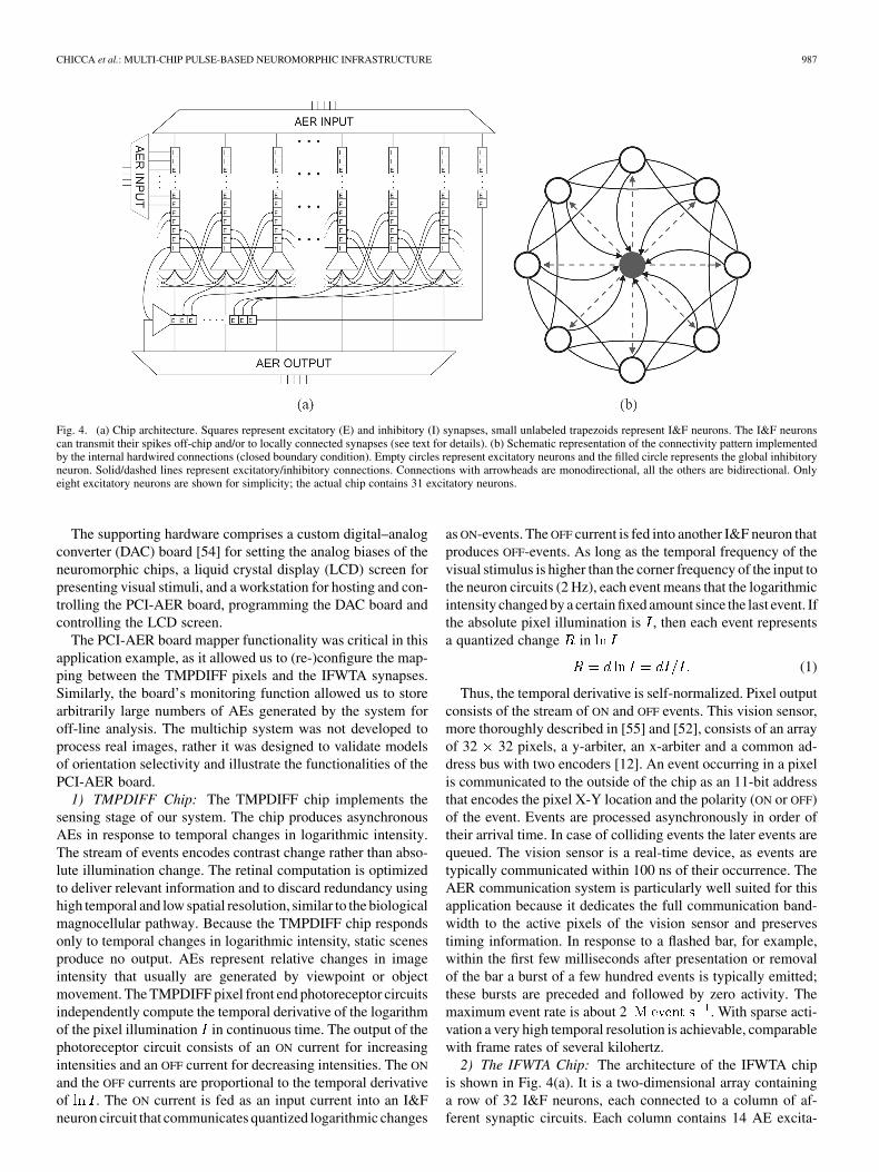
Fig. 4. (a) Chip architecture. Squares represent excitatory (E) and inhibitory (I) synapses, small unlabeled trapezoids represent I&F neurons. The I&F neuronscan transmit their spikes off-chip and/or to locally connected synapses (see text for details). (b) Schematic representation of the connectivity pattern implementedby the internal hardwired connections (closed boundary condition). Empty circles represent excitatory neurons and the filled circle represents the global inhibitoryneuron. Solid/dashed lines represent excitatory/inhibitory connections. Connections with arrowheads are monodirectional, all the others are bidirectional. Onlyeight excitatory neurons are shown for simplicity; the actual chip contains 31 excitatory neurons.
The supporting hardware comprises a custom digital–analogconverter (DAC) board [54] for setting the analog biases of theneuromorphic chips, a liquid crystal display (LCD) screen forpresenting visual stimuli, and a workstation for hosting and con-trolling the PCI-AER board, programming the DAC board andcontrolling the LCD screen.
The PCI-AER board mapper functionality was critical in thisapplication example, as it allowed us to (re-)configure the map-ping between the TMPDIFF pixels and the IFWTA synapses.Similarly, the board’s monitoring function allowed us to storearbitrarily large numbers of AEs generated by the system foroff-line analysis. The multichip system was not developed toprocess real images, rather it was designed to validate modelsof orientation selectivity and illustrate the functionalities of thePCI-AER board.
1) TMPDIFF Chip: The TMPDIFF chip implements thesensing stage of our system. The chip produces asynchronousAEs in response to temporal changes in logarithmic intensity.The stream of events encodes contrast change rather than abso-lute illumination change. The retinal computation is optimizedto deliver relevant information and to discard redundancy usinghigh temporal and low spatial resolution, similar to the biologicalmagnocellular pathway. Because the TMPDIFF chip respondsonly to temporal changes in logarithmic intensity, static scenesproduce no output. AEs represent relative changes in imageintensity that usually are generated by viewpoint or objectmovement. The TMPDIFF pixel front end photoreceptor circuitsindependently compute the temporal derivative of the logarithmof the pixel illumination in continuous time. The output of thephotoreceptor circuit consists of an ON current for increasingintensities and an OFF current for decreasing intensities. The ON
and the OFF currents are proportional to the temporal derivativeof . The ON current is fed as an input current into an I&Fneuron circuit that communicates quantized logarithmic changes
as ON-events. The OFF current is fed into another I&F neuron thatproduces OFF-events. As long as the temporal frequency of thevisual stimulus is higher than the corner frequency of the input tothe neuron circuits (2 Hz), each event means that the logarithmicintensity changed by a certain fixed amount since the last event. Ifthe absolute pixel illumination is , then each event representsa quantized change in
(1)
Thus, the temporal derivative is self-normalized. Pixel outputconsists of the stream of ON and OFF events. This vision sensor,more thoroughly described in [55] and [52], consists of an arrayof 32 32 pixels, a y-arbiter, an x-arbiter and a common ad-dress bus with two encoders [12]. An event occurring in a pixelis communicated to the outside of the chip as an 11-bit addressthat encodes the pixel X-Y location and the polarity (ON or OFF)of the event. Events are processed asynchronously in order oftheir arrival time. In case of colliding events the later events arequeued. The vision sensor is a real-time device, as events aretypically communicated within 100 ns of their occurrence. TheAER communication system is particularly well suited for thisapplication because it dedicates the full communication band-width to the active pixels of the vision sensor and preservestiming information. In response to a flashed bar, for example,within the first few milliseconds after presentation or removalof the bar a burst of a few hundred events is typically emitted;these bursts are preceded and followed by zero activity. Themaximum event rate is about 2 . With sparse acti-vation a very high temporal resolution is achievable, comparablewith frame rates of several kilohertz.
2) The IFWTA Chip: The architecture of the IFWTA chipis shown in Fig. 4(a). It is a two-dimensional array containinga row of 32 I&F neurons, each connected to a column of af-ferent synaptic circuits. Each column contains 14 AE excita-

988 IEEE TRANSACTIONS ON CIRCUITS AND SYSTEMS—I: REGULAR PAPERS, VOL. 54, NO. 5, MAY 2007
tory synapses, 2 AE inhibitory synapses and 6 locally connected(hardwired) synapses. When an AE is received, the synapse withthe corresponding row and column address is stimulated. If thesynaptic current resulting from the AEs routed to the neuron in-tegrates to the neuron’s voltage threshold for spiking, then thatneuron generates an AE which is transmitted off-chip. The AEinput synapses can be used to implement arbitrary network ar-chitectures, by (re)mapping AEs via the PCI-AER board.
Synapses with local hardwired connectivity are used to re-alize a cooperative-competitive network with recurrent interac-tions [see Fig. 4(b)]: 31 neurons of the array send their spikesto 31 local excitatory synapses on the global inhibitory neuron;the inhibitory neuron, in turn, stimulates the local inhibitorysynapses of the 31 excitatory neurons; each excitatory neuronstimulates its first and second neighbors on both sides usingtwo sets of locally connected excitatory synapses. The first andsecond neighbor connections of the neurons at the edges ofthe array are connected to pads. This allows us to leave thenetwork open, or implement closed boundary conditions (toform a ring of neurons [56]), using off-chip jumpers. The localsynapses are nonlinear integrators which produce analog cur-rents in response to digital input spikes. The local hardwiredconnectivity was implemented as described above in order toreduce AER bandwidth usage, while trying to keep the addi-tional area occupied small with respect to the overall networksize. Furthermore, it provides the flexibility to use the chip as astandalone module for single-chip experiments in which thereis no need for mapping.
All of the synapses on the chip can be switched off by ap-propriately setting the external bias voltages that control theirsynaptic weights; the local and AER synapses are controlled byindependent bias voltages. This allows us to inactivate either thelocal or the AE synaptic connections, or to use them in some ar-bitrary combination. A detailed description of the IFWTA chipwas presented in [53], [57].
B. Orientation Selectivity Experiments
In our application example, broad orientation selectivity isachieved by appropriately mapping feedforward connectionsfrom the TMPDIFF pixels to the IFWTA chip neurons (via thePCI-AER board), and it is sharpened by activating the localrecurrent connections on the IFWTA chip. The feedforwardmapping is set so that each IFWTA neuron collects all theTMPDIFF ON and OFF events that belong to a bar with aspecific orientation and position (discarding polarity), as shownin Fig. 5. We mapped 31 different groups of TMPDIFF pixelsonto 31 neurons of the IFWTA chip so as to form 31 differentlyoriented receptive fields. The orientations of these receptivefields are indicated by the bars shown as insets in Fig. 6(a).
In our experiments we displayed to the TMPDIFF chip ori-ented white bars on a dark background, flashing on an LCDscreen. The activity of the TMPDIFF chip was monitored by thePCI-AER board and transmitted (via the PCI-AER board map-ping tables) to the IFWTA chip. Using the PCI-AER board, wetime-stamped and logged both the TMPDIFF and IFWTA AEsfor data analysis. To characterize the system we collected thesystem’s activity in response to bars of 30 different orientations(6 degrees apart from each other) chosen independently of the
Fig. 5. Sketch representative of the mapping from the TMPDIFF chip to theIFWTA chip. The TMPDIFF retina is represented by a twelve by twelve arrayof pixels, lines represents excitatory connections from the TMPDIFF chip toneurons of the IFWTA chip (represented by circles).
set of pre-wired preferred orientations. Each oriented bar wasflashed at a rate of about 2.5 Hz, producing one ON and one OFF
transition per cycle and the AE data was monitored for 25 sec-onds. Because it was not easy to synchronize the stimulus onsetwith the start of the monitoring, we decided to start the mon-itoring 5 s after executing the command to start the stimulus.In this way, we were sure that the stimulus was already presentwhen we started monitoring.
We repeated the same experiment for two different condi-tions in terms of the local connectivity of the WTA chip. Inthe first condition the biases of the WTA chip were set to im-plement a purely feedforward model: local recurrent synapseswere inactive and the neurons’ inputs were completely deter-mined by the activity of the retinal pixels. Subsequently, weactivated the recurrent connectivity to implement the feedbackmodel maintaining all other parameters unchanged. Three setsof local synapses were used to implement the feedback model:1) first neighbor excitatory to excitatory synapses to simulatethe mutually excitatory connections among cells with similarpreferred orientations; 2) inhibitory and 3) excitatory synapsesconnecting the global inhibitory neuron to the excitatory neu-rons and vice versa to simulate the mutual inhibition amongcells with different preferred orientations [see Fig. 4(b)]. Theeffect of competition alone is described in [57].
Orientation tuning curves (i.e., graphs of neural responseversus stimulus orientation) are typically measured in experi-ments related to the characterization of orientation selectivityin visual cortical neurons. We applied the same analysis to ourdata: the recorded activity of the WTA neurons was used tocompute the mean firing rate of each neuron in response to thestimuli and tuning curves were obtained by plotting these datafor each neuron as a function of stimulus orientation. Fig. 6(a)shows the computed tuning curves for each neuron of theIFWTA. Each sub-figure represents the mean response of theneuron to different orientations. The inset in each sub-figurerepresents the retinal pixels mapped to that particular neuron.

CHICCA et al.: MULTI-CHIP PULSE-BASED NEUROMORPHIC INFRASTRUCTURE 989
Fig. 6. Tuning curves for the feedforward (dashed line) and the feedback (solid line) model of orientation selectivity. (a) The mean frequency (hertz) of each neuronis plotted as a function of stimulus orientation [the scales are the same for all plots and can be seen in (b)]. The top left graph shows the activity of the inhibitoryneuron, the other graphs show the activity of the excitatory neurons (a bar representing the retinal pixels mapped to the neuron, i.e., its preferred orientation, isshown in each plot). The tuning curves of the feedforward model have a larger amplitude and a smaller half-width at half-height compared to the tuning curvesof the feedback model. (b) Tuning curves for the feedforward (dashed line and filled circles) and the feedback (solid line and empty circles) model of orientationselectivity for the neuron with vertical preferred orientation [enlargement of the second from left panel in the first row of (a)]. The lines represent the von Misesfunctions fitted to the data, represented by circles and error bars (standard deviation over the measured mean frequency.)
The TMPDIFF central pixels are mapped to all neurons,therefore each WTA neuron is also receiving input events whenits nonpreferred orientation is presented to the retina. The effectof this “base line” input is clearly visible in the feedforwardmodel, where the activity of the WTA neurons simply reflectsthe input from the retina. In this case, the frequencies in thetuning curves are greater than zero for all orientations anda maximum is observed at the preferred orientation. In thefeedback model the “base line” activity is suppressed and theactivity in response to the preferred orientation is amplified.
We fitted the tuning curves to quantitatively estimate the ef-fect of recurrent connectivity on the response of the orientationselective neurons. We used a von Mises function as the fittingfunction [58], defined as
(2)
where is the value of the function at the preferred orientation, and is a width parameter, from which the half-width at
half-height may be calculated (in radians) as:
(3)
The von Mises function approximates a Gaussian in shape overa biologically likely range of values of . A least-squares fit ofthe data to the von Mises function was used to estimate the pa-rameters of the tuning curve of each selective oriented neuron.Fig. 6(b) shows the tuning curve of the neuron tuned to verticalorientation: the data and the von Mises fitted function are plottedfor both the feedforward and feedback model. The data pointsused to perform the fits are the mean frequencies of the neuronscomputed over the 25 s of data acquisition. The IFWTA chipis stimulated only during and shortly after the appearance anddisappearance of the bar, when the ON and OFF pixels of the TM-PDIFF chip are activated by the visual stimulation. High vari-ability is then induced in the pattern of activity of the TMPDIFF
Fig. 7. Raster plot of the response of the TMPDIFF pixels and IFWTA neu-rons to a vertical bar. The graphs in the top row show the ON (black dots) andOFF (grey dots) response of the TMPDIFF chip (top) and the response of theIFWTA chip (bottom) to two cycles of the flashing stimulus. The graphs in thebottom row show a magnified versions of one of the bursts of the top row graphs.In the left column the IFWTA is configured to implement the purely feedfor-ward model. In the right column the IFWTA chip implements the recurrent net-work described in the text. This graphs show how the orientation selectivitysystem produces bursts of activity in response to the appearing/disappearing ofthe flashing bars and no activity when the stimulus is static. As shown by thetwo graphs in the second row, the response delays of the feedforward networkand feedback network are comparable.
and IFWTA chips (see Fig. 7), with bursts of events during theappearance and disappearance of the flashing bar and gaps ofno activity in between. Ideally, the spike rate during each singleburst should be measured and considered as a single measure-ment. The mean and standard deviation over many repetitions ofthis measurement would provide a good estimation of the meanfrequency and its variation. To allow a simpler manipulation ofthe data and start from a more reliable “single” measurement

990 IEEE TRANSACTIONS ON CIRCUITS AND SYSTEMS—I: REGULAR PAPERS, VOL. 54, NO. 5, MAY 2007
Fig. 8. Population data for the amplitude of the tuning curve at the preferredorientation (feedback versus feedforward model).
Fig. 9. Population data for the half-width at half-height of the tuning curve(feedback versus feedforward model).
we decided to divide our 25-s acquisition time into five 5-s in-tervals, and consider the means over these intervals as singlemeasurements of the neurons’ mean frequencies in response tothe stimulus. The variability of our data [shown as error bars inFig. 6(b)] is then computed as the standard deviation over thefive measured frequencies.
To evaluate the goodness of the fits we used the R-squarevalue (the square of the correlation between the measured valuesand the values predicted by the fit). It can take on any valuebetween 0 and 1, with a value closer to 1 indicating a betterfit. We calculated R-square for all the fits: the mean of all thecomputed values is 0.982 with a standard deviation of ,which indicates that on average the fits can explain 98% of thetotal variation in the data.
Figs. 8 and 9 show the estimated amplitude and half-widthat half-height respectively, for all the neurons in the network inthe feedback versus the feedforward configuration. All neuronslie above the diagonal in Fig. 8, showing that the response tothe preferred orientation is amplified in the feedback networkwith respect to the response in the purely feedforward network.Sharpening of the tuning is shown in Fig. 9, where neurons tend
TABLE IIPARAMETERS OBTAINED BY LEAST-SQUARES FITTING OF THE DATA TO THE
VON MISES DISTRIBUTION. THE MEAN AND STANDARD DEVIATION OVER THE
POPULATION OF 31 ORIENTATION SELECTIVE NEURONS
to lie below the diagonal. The population mean values of theseparameters plus the baseline activity and the preferred orienta-tion error are listed in Table II. On average the peak activity inthe feedback network is twice the peak activity in the feedfor-ward network and the ratio between the half-width at half-heightfor the two configurations is 0.9 (feedback over feedforward).
IV. CONCLUSION AND OUTLOOK
We have presented a flexible hardware/software infrastructurefor building complex neuromorphic systems using the AER. Itprovides monitoring, sequencing and mapping functions easilyaccessible through the software interface and it allows conve-nient and rapid prototyping (e.g., by stimulating, monitoringand/or experimenting with different address-space mappings).The PCI-AER board is therefore an ideal tool for developingsingle and multichip AER systems. Additional applicationexamples that rely on this PCI-AER board have been recentlypresented in [2], [29], [59]–[61]. This infrastructure and itsdocumentation has reached the point at which it can be easilyused by researchers and labs which were not involved in itsdevelopment. At the time of writing, five such labs have acquiredone or more boards each. Some users have written small C orC++ applications for spike-train generation and data loggingdirectly using the library Application Programming Interface(API). A Matlab toolbox [62] has been developed for the off-linegeneration of spike trains to be sent to the PCI-AER board viathe library and driver. A client-server architecture [29] has alsobeen developed on top of the library to enable the use of the boardon-line from within Matlab, including real-time data display.
Future developments should include a refinement of thisclient-server architecture to enable multiple data-sinks to readthe monitored AE stream concurrently in a coordinated way.Other possible future developments include Java support, and astimulation tool for the on-line generation of AE patterns to drivethe sequencer. The instrumentation of the driver and consequentavailability of performance data will aid the assessment of thepresent communication infrastructure, and can be used to guidefuture driver optimization work. The library could also be portedto other AER monitoring, mapping and sequencing hardwareproviding cross-platform compatibility for higher level software.
We presented the implemented orientation selectivity systemcomposed of a sensing stage (the TMPDIFF chip) and a com-putational module (the IFWTA) not explicitly designed for thispurpose by using a specific mapping between the two chips.We showed how the recurrent connectivity in the computa-tional module has an effect on the response to oriented stimuli

CHICCA et al.: MULTI-CHIP PULSE-BASED NEUROMORPHIC INFRASTRUCTURE 991
similar to those described in theoretical models of orientationselectivity.
This experiment demonstrates the feasibility of real-timeAER-based inter-chip communication through the PCI-AERinterface. The orientation selectivity system was assembledexploiting the monitoring and mapping functionality of thePCI-AER board, thereby demonstrating the capabilities ofthe board. Other experiments exploiting the monitor and se-quencing functionality have been described elsewhere (e.g.,[2], [63]–[65]).
ACKNOWLEDGMENT
The authors thank their colleagues at the Institute of Neuroin-formatics for designing and providing the digital–analog con-verter board (S. Zahnd and M. Oster), for help in implementingthe stimuli (F. Roth), and analyzing the data (C. Girardin).
REFERENCES
[1] W. Maass and C. M. Bishop, Pulsed Neural Networks. Cambridge,MA: MIT Press, 1998.
[2] G. Indiveri, E. Chicca, and R. Douglas, “A VLSI array of low-powerspiking neurons and bistable synapses with spike-timing dependentplasticity,” IEEE Trans. Neural Netw., vol. 17, no. 1, pp. 211–221, Jan.2006.
[3] F. Tenore, J. Vogelstein, R. Etienne-Cummings, G. Cauwenberghs, andP. Hasler, “A floating-gate programmable array of silicon neurons forcentral pattern generating networks,” in Proc. IEEE Int. Symp. CircuitsSyst., 2006, pp. 3157–3160.
[4] P. Merolla and K. Boahen, “A recurrent model of orientation mapswith simple and complex cells,” in Advances in Neural InformationProcessing Systems. Cambridge, MA: MIT Press, Dec. 2004, vol. 16,pp. 995–1002.
[5] E. Chicca, D. Badoni, V. Dante, M. D’Andreagiovanni, G. Salina, S.Fusi, and P. Del Giudice, “A VLSI recurrent network of integrate-and-fire neurons connected by plastic synapses with long term memory,”IEEE Trans. Neural Netw., vol. 14, no. 5, pp. 1297–1307, Sep. 2003.
[6] R. J. Vogelstein, F. Tenore, R. Philipp, M. S. Adlerstein, D. H. Gold-berg, and Cauwenberghs, “Spike timing-dependent plasticity in the ad-dress domain,” in Advances in Neural Information Processing Sys-tems. Cambridge, MA: MIT Press, 2003.
[7] D. Goldberg, G. Cauwenberghs, and A. Andreou, “Probabilisticsynaptic weighting in a reconfigurable network of VLSI integrate-and-fire neurons,” Neural Netw., vol. 14, no. 6–7, pp. 781–793, Sep. 2001.
[8] G. Indiveri, T. Horiuchi, E. Niebur, and R. Douglas, “A competitivenetwork of spiking VLSI neurons,” in World Congress on Neuroinfor-matics, ser. ARGESIM Rep. no. 20, F. Rattay, Ed. Vienna, Austria:ARGESIM/ASIM-Verlag, 2001, pp. 443–455.
[9] M. Mahowald, “VLSI analogs of neuronal visual processing: a syn-thesis of form and function,” Ph.D. dissertation, Dep. Comput. Neur.Syst., California Institute of Technology, Pasadena, CA, 1992.
[10] J. Lazzaro, J. Wawrzynek, M. Mahowald, M. Sivilotti, and D. Gillespie,“Silicon auditory processors as computer peripherals,” IEEE Trans.Neural Netw., vol. 4, no. 3, pp. 523–528, May 1993.
[11] The address-event representation communication protocol AER 0.02,Caltech, Pasadena, CA, Internal Memo, Feb. 1993 [Online]. Available:http://www.ini.uzh.ch/~amw/scx/std002.pdf
[12] K. Boahen, “Communicating neuronal ensembles between neuromor-phic chips,” in Neuromorphic Systems Engineering, T. S. Lande, Ed.Norwell, MA: Kluwer Academic, 1998, pp. 229–259.
[13] K. A. Boahen, “Point-to-point connectivity between neuromorphicchips using address-events,” IEEE Trans. Circuits Syst. II, AnalogDigit. Signal Process., vol. 47, no. 5, pp. 416–434, May 2000.
[14] K. A. Boahen, “A burst-mode word-serial address-event link—I:Transmitter design,” IEEE Circuits Syst. I, Reg. Papers, vol. 51, no. 7,pp. 1269–1280, Jul. 2004.
[15] Z. Kalayjian and A. Andreou, “Asynchronous communication of 2-Dmotion information using winner-takes-all arbitration,” in Neuromor-phic Systems Engineering, T. S. Lande, Ed. Norwell, MA: KluwerAcademic, 1998, pp. 217–227.
[16] E. Culurciello, R. Etienne-Cummings, and K. Boahen, “Arbitrated ad-dress-event representation digital image sensor,” Electron. Lett., vol.37, no. 24, pp. 1443–1445, Nov. 2001.
[17] P. Lichtsteiner, C. Posch, and T. Delbrück, “A 128 � 128 120 dB30 mW asynchronous vision sensor that responds to relative intensitychange,” in Dig. Tech. Papers IEEE ISSCC , 2006, pp. 508–509.
[18] A. van Schaik and S.-C. Liu, “AER EAR: A matched silicon cochleapair with address event representation interface,” in Proc. IEEE Int.Symp. Circuits Syst., May 2005, vol. V, pp. 4213–4216.
[19] G. Indiveri, A. Whatley, and J. Kramer, “A reconfigurable neuromor-phic VLSI multichip system applied to visual motion computation,”in Proc. 7th Int. Conf. Microelectronics for Neural, Fuzzy and Bio-Inspired Systems; Microneuro’99, Los Alamitos, CA, Apr. 1999, pp.37–44.
[20] S. R. Deiss, R. J. Douglas, and A. M. Whatley, “A pulse-coded commu-nications infrastructure for neuromorphic systems,” in Pulsed NeuralNetworks, W. Maass and C. M. Bishop, Eds. Cambridge, MA: MITPress, 1998, ch. 6, pp. 157–178.
[21] A. Mortara, E. Vittoz, and P. Venier, “A communication scheme foranalog VLSI perceptive systems,” IEEE J. Solid-State Circuits, vol. 30,no. 6, pp. 660–669, Jun. 1995.
[22] V. Dante, P. Del Giudice, and A. M. Whatley, “PCI-AER—hard-ware and software for interfacing to address-event based neuro-morphic systems,” The Neuromorphic Engineer vol. 2, no. 1, pp.5–6, 2005 [Online]. Available: http://ine-web.org/research/newslet-ters/index.html
[23] R. Serrano-Gotarredona, M. Oster, P. Lichtsteiner, A. Linares-Barranco, R. Paz-Vicente, F. Gómez-Rodríguez, H. K. Riis, T.Delbrück, S. C. Liu, S. Zahnd, A. M. Whatley, R. J. Douglas, P.Häfliger, G. Jimenez-Moreno, A. Civit, T. Serrano-Gotarredona, A.Acosta-Jiménez, and B. Linares-Barranco, “AER building blocks formulti-layer multi-chip neuromorphic vision systems,” in Advancesin Neural Information Processing Systems, S. Becker, S. Thrun,and K. Obermayer, Eds. Cambridge, MA: MIT Press, Dec. 2005,vol. 15.
[24] D. P. M. Northmore and J. G. Elias, “Building silicon nervous sys-tems with dendritic tree neuromorphs,” in Pulsed Neural Networks, W.Maass and C. M. Bishop, Eds. Cambridge, MA: MIT Press, 1998, ch.5, pp. 135–156.
[25] C. M. Higgins and C. Koch, “A modular multi-chip neuromorphic ar-chitecture for real-time visual motion processing,” Anal. Integr. Cir-cuits Signal Process., vol. 24, pp. 195–211, 2000.
[26] P. Merolla and K. Boahen, “Dynamic computation in a recurrent net-work of heterogeneous silicon neurons,” in Proc. IEEE Int. Symp. Cir-cuits Syst, May 2006, pp. 4539–4542.
[27] F. Gomez-Rodriguez, R. Paz, A. Linares-Barranco, M. Rivas, L. Miro,S. Vicente, G. Jimenez, and A. Civit, “AER tools for communicationsand debugging,” in Proc. IEEE Int. Symp. Circuits Syst., 2006, pp.3253–3256.
[28] R. Berner, “High-speed USB2.0 AER interfaces,” Diploma thesis,Dept. Elect. Eng., University of Züurich, ETH Züurich, and Univer-sidad de Sevilla, Zurich, Switzerland, 2006.
[29] M. Oster, A. M. Whatley, S.-C. Liu, and R. J. Douglas, “A hard-ware/software framework for real-time spiking systems,” in Proc. 15thInternational Conf. Artificial Neural Netw.: Biological Inspirations(ICANN’05) , , W. Duch, J. Kacprzyk, and E. Oja, Eds. et al., Warsaw,Poland, Sep. 11–14, 2005, vol. 3696, pp. 161–166.
[30] R. J. Douglas and K. A. C. Martin, “Neural circuits of the neocortex,”Annu. Rev. Neurosci., vol. 27, pp. 419–451, 2004.
[31] R. Douglas, K. Martin, and D. Whitteridge, “A canonical microcircuitfor neocortex,” Neural Comput., vol. 1, pp. 480–488, 1989.
[32] D. Hubel and T. Wiesel, “Receptive fields, binocular interaction andfunctional architecture in the cat’s visual cortex,” J. Physiol., vol. 160,pp. 106–154, 1962.
[33] D. Ferster and K. D. Miller, “Neural mechanisms of orientation selec-tivity in the visual cortex,” Annu. Rev. Neurosci., vol. 23, pp. 441–471,2000.
[34] H. Sompolinsky and R. Shapley, “New perspective on the mechanismsfor orientation selectivity,” Current Opinion Neurobiol., vol. 7, pp.514–522, 1997.
[35] T. W. Troyer, A. E. Krukowski, N. J. Priebe, and K. D. Miller, “Con-trast-invariant orientation tuning in cat visual cortex: Thalamocorticalinput tuning and correlation-based intracortical connectivity,” J. Neu-rosci., vol. 18, no. 15, pp. 5908–5927, 1998.
[36] R. Shapley, M. Hawken, and D. L. Ringach, “Dynamics of orientationselectivity in the primary visual cortex and the importance of corticalinhibition,” Neuron, vol. 38, pp. 689–699, 2003.

992 IEEE TRANSACTIONS ON CIRCUITS AND SYSTEMS—I: REGULAR PAPERS, VOL. 54, NO. 5, MAY 2007
[37] D. C. Somers, S. B. Nelson, and M. Sur, “An emergent model of orien-tation selectivity in cat visual cortical simple cells,” J. Neurosci., vol.15, pp. 5448–5465, 1995.
[38] R. Ben-Yishai, R. Lev Bar-Or, and H. Sompolinsky, “Theory of orien-tation tuning in visual cortex,” Proc. Nat. Acad. Sci., vol. 92, no. 9, pp.3844–3848, Apr. 1995.
[39] R. J. Douglas, M. A. Mahowald, and K. A. C. Martin, “Hybrid analog-digital architectures for neuromorphic systems,” in Proc. IEEE WorldCongr. Comput. Intell., 1994, vol. 3, pp. 1848–1853.
[40] T. Serrano-Gotarredona, A. G. Andreou, and B. Linares-Barranco,“AER imager filtering architecture for vision-processing systems,”IEEE Trans. Circuits Syst. I, Fundam. Theory Appl., vol. 46, no. 9, pp.1064–1071, Sep. 1999.
[41] G. Cauwenberghs and J. Waskiewicz, “Focal-plane analog VLSI cel-lular implementation of the boundary contour system,” IEEE Trans.Circuits Syst. I, Fundam. Theory Appl., vol. 46, no. 2, pp. 1064–1071,Feb. 1999.
[42] B. E. Shi, “A low-power orientation-selective vision sensor,” IEEETrans. Circuits Syst. II, Analog Digit. Signal Process., vol. 47, no. 5,pp. 435–440, May 2000.
[43] P. Venier, A. Mortara, X. Arreguit, and E. A. Vittoz, “An integratedcortical layer for orientation enhancement,” IEEE J. Solid-State Cir-cuits, vol. 32, no. 2, pp. 177–186, Feb. 1997.
[44] S.-C. Liu, J. Kramer, G. Indiveri, T. Delbruck, T. Burg, and R. Douglas,“Orientation-selective aVLSI spiking neurons,” Neural Netw., vol. 14,no. 6/7, pp. 629–643, 2001.
[45] T. Y. W. Choi, P. A. Merolla, J. V. Arthur, K. A. Boahen, and B. E. Shi,“Neuromorphic implementation of orientation hypercolumns,” IEEETrans. Circuits Syst. I, Reg. Papers, vol. 52, no. 6, pp. 1049–1060, Jun.2005.
[46] K. Shimonomura and T. Yagi, “An orientation-selective multi-chipaVLSI applicable to texture analysis,” in Proc. Int. Joint Conf. NeuralNetw., 2005, pp. 3267–3271.
[47] U. Mallik, R. J. Vogelstein, E. Culurciello, R. Etienne-Cummings, andG. Cauwenberghs, “A real-time spike-domain sensory information pro-cessing system,” in Proc. IEEE Int. Symp. Circuits Syst., 2005, vol. 3,pp. 1919–1922.
[48] S. R. Deiss, T. Delbrück, R. J. Douglas, M. Fischer, M. Mahowald,T. Matthews, and A. M. Whatley, Address-event asynchronous localbroadcast protocol, Inst. Neuroinform., Zurich, Switzerland, 1994 [On-line]. Available: http://www.ini.uzh.ch/~amw/scx/aeprotocol.html,
[49] A. M. Whatley, PCI-AER Board Driver, Library & Documentation,Inst. Neuroinform., Zurich, Switzerland, 2007 [Online]. Available:http://www.ini.uzh.ch/~amw/pciaer/
[50] AMCC, PCI Products data book, Section 2: S5920 PCI target interface,, Applied Micro Circuits Corporation, San Diego, CA, 1998 [Online].Available: http://www.amcc.com
[51] R. Paz-Vincente, A. Linares-Barranco, D. Cascado, M. Rodriguez, G.Jimenez, A. Civit, and J. Sevillano, “PCI-AER interface for neuro-in-spired spiking systems,” in Proc. IEEE Int. Symp. Circuits Syst., 2006,pp. 3253–3256.
[52] P. Lichtsteiner, T. Delbruck, and J. Kramer, “Improved ON/OFF tem-poraly differentiating address-event imager,” in Proc. 11th IEEE Int.Conf. Electronics, Circuits Syst., Dec. 2004, pp. 211–214.
[53] E. Chicca, G. Indiveri, and R. J. Douglas, “An event based VLSI net-work of integrate-and-fire neurons,” in Proc. IEEE Int. Symp. CircuitsSyst., 2004, pp. V-357–V-360.
[54] M. Oster, “Tuning aVLSI chips with a mouse click,” Neuromorph.Eng. vol. 2, no. 1, p. 9, 2005 [Online]. Available: http://ine-web.org/re-search/newsletters/index.html
[55] J. Kramer, “An integrated optical transient sensor,” IEEE Trans. Cir-cuits Syst. II, Analog Digit. Signal Process., vol. 49, no. 9, pp. 612–628,Sep. 2002.
[56] R. Hahnloser, R. Sarpeshkar, M. Mahowald, R. J. Douglas, and S.Seung, “Digital selection and analog amplification co-exist in anelectronic circuit inspired by neocortex,” Nature, vol. 405, no. 6789,pp. 947–951, 2000.
[57] E. Chicca, “A neuromorphic VLSI system for modeling spike-basedcooperative competitive neural networks,” Ph.D. dissertation, Dept.Phys., ETH Zürich, Zürich, Switzerland, Apr. 2006.
[58] N. V. Swindale, “Orientation tuning curves: Empirical description andestimation of parameters,” Biolog. Cybern., vol. 78, pp. 45–56, 1998.
[59] S. Mitra, S. Fusi, and G. Indiveri, “A VLSI spike-driven dynamicsynapse which learns,” in Proc. IEEE Int. Symp. Circuits Syst., May2006, pp. 2777–2780.
[60] C. Bartolozzi and G. Indiveri, “Silicon synaptic homeostasis,” in Proc.Brain Inspired Cogn. Syst. , 2006, pp. 1–6.
[61] E. Chicca, P. Lichtsteiner, T. Delbruck, G. Indiveri, and R. J. Dou-glas, “Modeling orientation selectivity using a neuromorphic multichipsystem,” in Proc. IEEE Int. Symp. Circuits Syst., 2006, pp. 1235–1238.
[62] D. Muir, Spike Toolbox [Online]. Available: http://www.ini.uzh.ch/~dylan/spike_toolbox/ 2005
[63] G. Indiveri, “VLSI reconfigurable networks of integrate-and-fire neu-rons with spike-timing dependent plasticity,” Neuromorph. Eng. vol. 2,no. 1, pp. 4–7, 2005 [Online]. Available: http://ine-web.org/research/newsletters/index.html
[64] C. Bartolozzi and G. Indiveri, “Selective attention implemented withdynamic synapses and integrate-and-fire neurons,” Neurocomput., vol.69, pp. 1971–1976, 2005.
[65] M. Oster and S.-C. Liu, “Spiking inputs to a winner-take-all network,”in Advances in Neural Information Processing Systems (NIPS), Y.Weiss, B. Schölkopf, and J. Platt, Eds. Cambridge, MA: MIT Press,Dec. 2005, vol. 18, Neural Information Processing Systems Founda-tion, pp. 1051–1058.
Elisabetta Chicca (M’06) received the Laurea(equivalent to M.S.) degree in physics from theUniversity of Rome La Sapienza, Rome, Italy, andthe Ph.D. degree from the Swiss Federal Institute ofTechnology (ETHZ), Zurich, Switzerland, in 1999and 2006, respectively.
She is currently a Postdoctoral Fellow at theInstitute of Neuroinformatics, University of Zurich,Zurich, Switzerland, and UZH-ETHZ. Her researchinterests include neuromorphic analog VLSI modelsof cortical circuits and learning.
Dr. Chicca is currently a member of the IEEE BioCAS technical committee.
Adrian M. Whatley received the B.Sc. degree inchemistry from the University of Bristol, Bristol,U.K., in 1986.
After working for almost ten years in the Britishcomputer industry, he took up his current softwareengineering position at the Institute of Neuroinfor-matics, University of Zurich, Zurich, Switzerland,where he works primarily on address-event commu-nication systems.
Patrick Lichtsteiner received the Diploma (equiva-lent to M.S.) degree in physics and the Ph.D. degreefrom the Swiss Federal Institute of Technology(UZH-ETHZ), Zurich, Switzerland, in 2002 and2006, respectively.
He is currently working for the Institute ofNeuroinformatics, University of Zurich, Zurich,Switzerland, and ETHZ. His research interests in-clude CMOS imaging, neuromorphic vision sensorsand high-speed vision.
Vittorio Dante received the electronics diplomafrom ITIS Enrico Fermi, Rome, Italy, in 1983.
He has been an Electronics Designer working onmicrocontrollers and embedded systems (from 1980to 1990). Since 1990, he has been with the PhysicsLaboratory, Italian National Institutes of Health,Rome Italy. In the framework of Italian NationalInstitute for Nuclear Physics (INFN) projects, heworked on systems based on VME, PCI, and FB+buses. Since 1997, he has been involved in researchon efficient communication in neuromorphic multi-
chip systems.
CHICCA et al.: MULTI-CHIP PULSE-BASED NEUROMORPHIC INFRASTRUCTURE 993
Tobias Delbruck (M’99–SM’06) received the B.S.degree in physics and applied mathematics and thePh.D. degree in computation and neural systemsfrom California Institute of Technology (Caltech),Pasadena, CA, in 1993.
He worked for several years for Arithmos, Synap-tics, National Semiconductor, and Foveon, wherehe was one of the Founding Employees. In 1998 hemoved to Switzerland to join the Institute of Neu-roinformatics (INI), University of Zurich, Zurich,Switzerland, where he is currently a Group Leader.
In 2002, he was a Lead Developer of the tactile luminous floor used in INI’sexhibit “Ada: Playful Intelligent Space.” He is currently also a Visiting Sci-entist at Caltech. His main interest is in developing neuromorphic electronics,particularly vision sensor chips. Prior to working for Arithmos, he co-inventedthe standard neuromorphic adaptive photoreceptor circuit and bump circuit. Hehas been awarded eight patents, and has over 30 refereed papers in journals andconferences, 4 book chapters, and 1 book.
Dr. Delbruck and his students have been awarded 4 prizes for IEEE confer-ence papers, including the 2006 ISSCC Best European Paper Award.
Paolo Del Giudice received the graduate degree inphysics from the Rome University “La Sapienza,”Rome, Italy, in 1985.
Since 1991, he has been with at the ComplexSystems Unit, Technologies and Health Department,Italian National Institutes of Health, Rome Italy.He is also with the he National Institute of NuclearPhysics, Rome, Italy. He has been mostly active inthe theory, simulation and electronic implementationof neural network models, recently focusing inparticular of the collective stochastic dynamics of
spiking neurons and neuromorphic multichip systems. He also worked oncomputational problems in radiotherapy, and the statistical analysis of DNAsequences.
Rodney J. Douglas received degrees in science andmedicine and the Ph.D. degree in neuroscience fromthe University of Cape Town, Cape Town, SouthAfrica.
He joined the Anatomical NeuropharmacologyUnit, Oxford, U.K., where he continued his researchon the anatomy and biophysics of neocortical circuitstogether with K. Martin. He is currently a Professorof neuroinformatics and Co-Director of the Instituteof Neuroinformatics, Swiss Federal Institute ofTechnology, Zurich, Switzerland, and the University
of Zurich (UZH-ETHZ), Zurich, Switzerland. He was a Visiting Associate, andthen a Visiting Professor, at the California Institute of Technology, Pasadena,where he extended his research interests to neural computation to the modelingof cortical circuits using digital methods (together with C. Koch), and alsoby the fabrication of analog VLSI circuits (together with M. Mahowald). In1996, he and K. Martin joined the UZH-ETHZ, to establish the Institute ofNeuroinformatics.
Dr. Douglas was awarded the Korber Foundation Prize for European Sciencein 2000.
Giacomo Indiveri (SM’06) received the graduateand Ph.D. degrees in electronic engineering from thethe University of Genova, Genova, Italy.
He is an Assistant Professor at the Instituteof Neuroinformatics (INI), University of Zurich,Zurich, Switzerland. He was awarded a Fellowshipfor the Italian “National Research Program onBioelectronic technologies” (completed cum laudein 1995), and worked as a Post-Doctoral Fellowshipat the California Institute of Technology, Pasadena,from 1994 to 1996. His main interests are in the de-
sign and fabrication of neuromorphic electronic circuits that implement corticalprocessing and in the construction of spike-based learning, winner-take-allarchitectures, and hardware attentional systems.
Dr. Indiveri is member of numerous IEEE technical committees.