24 IEEE TRANSACTIONS ON CIRCUITS AND SYSTEMS–I: …
14
24 IEEE TRANSACTIONS ON CIRCUITS AND SYSTEMS–I: REGULAR PAPERS, VOL. 64, NO. 1, JANUARY 2017 A Class of 1-Bit Multi-Step Look-Ahead - Modulators Charis Basetas, Student Member, IEEE, Thanasis Orfanos, Student Member, IEEE, and Paul P. Sotiriadis, Senior Member, IEEE Abstract— Digital Multi-Step Look-Ahead (MSLA) 1-bit - modulators are introduced. They improve upon the stability and noise shaping characteristics of conventional 1-bit - modulators by minimizing quantization error metrics of the current and future output samples. The mathematical model of the proposed MSLA modulators is analyzed. It is shown that the MSLA modulators are equivalent to a system of conventional - modulators in parallel, but with a common multi-input 1-bit quantizer instead of a typical one. The properties of this multi- input quantizer are studied and the transfer functions of the MSLA modulators are derived. Simulation results are presented demonstrating the advantages of the MSLA modulators over conventional 1-bit - ones in a number of applications. A parametric hardware architecture of the MSLA modulators is presented offering an adjustable trade-off between performance and hardware complexity based on the number of look-ahead steps. Finally, a FPGA implementation of a MSLA modulator is presented along with simulation results. Index Terms—1-bit quantization, all-digital, DAC, look-ahead, modulator, noise shaping, optimization algorithm, sigma-delta. I. I NTRODUCTION T HE noise shaping characteristics and simplicity of - modulators have led to their widespread usage in high-resolution Digital-to-Analog Converters (DAC), Analog- to-Digital Converters (ADC) and time-to-digital converters. Initially, - modulators were designed as purely analog or mixed-signal circuits [1]. Because digital circuits are unaf- fected by process, voltage and temperature variations, and are becoming faster, more energy-efficient and smaller with the scaling of IC process technologies, there has been an increasing interest in all-digital - modulators [2]. These modulators are used as components in a variety of applications ranging from traditional data converters to all-digital transmit- ters [3], [4], frequency synthesizers [5], [6] and PLLs [7]. Moreover, a - DAC is the combination of an all-digital - modulator followed by a 1-bit or few-bit DAC, which is much easier to design than a multi-bit one. Since - modulation is based on a feedback loop, stability requirements are crucial for a successful design. These require- Manuscript received January 28, 2016; revised April 25, 2016 and July 13, 2016; accepted August 19, 2016. Date of publication October 26, 2016; date of current version January 6, 2017. This work was partially supported by Broadcom Foundation USA. This paper was recommended by Associate Editor P. Rombouts. The authors are with the National Technical University of Athens, Heroon Polytechniou 9, 15780 Zografou, Greece (e-mail: [email protected]; [email protected]; [email protected]). Color versions of one or more of the figures in this paper are available online at http://ieeexplore.ieee.org. Digital Object Identifier 10.1109/TCSI.2016.2608922 ments pose restrictions to the noise transfer function (NTF) design space and limit the allowable input signal range [1], [8]. The quantizer resolution of the - modulator also affects its stability [9]. Single-bit modulators are more susceptible to instability than multi-bit ones, but the tendency towards DAC-less all-digital architectures necessitates the use of 1-bit - modulators. Furthermore, 1-bit quantization is inherently linear since there are only two signal levels and thus the matching requirements between different components are significantly relaxed. Many works have dealt with the stability analysis of - modulators. Parallel decomposition of high-order modulators [10], limit cycle investigation [11] and quasi-linear modeling using the describing function method [12] are some of the proposed stability analysis techniques, while in [13] the stability of band-pass - modulators is considered. This work proposes an all-digital Multi-Step Look- Ahead (MSLA) 1-bit modulation scheme which improves on the stability of conventional - modulators. This is achieved by taking into account future input samples for the determination of the current output. The number of look-ahead steps is a design parameter which is selected in order to obtain the desired balance between complexity and stability improvement. The enhanced stability offers more flexibility in the selection of the NTF, allowing for NTFs with increased pass-band bandwidth and out-of-band gain. This results in higher in-band noise attenuation and thus higher signal-to- noise-ratio (SNR). In section II the process of 1-bit quantization is viewed as an optimization algorithm and the MSLA algorithm is introduced. The mathematical analysis of the MSLA modulator follows in section III, where its relation to conventional - and other look-ahead modulators is investigated. In section IV simulation results for a variety of applications are presented and the stability improvement offered by the MSLA modulator is quantified. Section V introduces a digital hardware architecture for the implementation of the MSLA modulator and a test- case FPGA implementation is presented. Finally, section VI concludes the discussion. II. 1-BIT QUANTIZATION AS AN OPTIMIZATION ALGORITHM The process of 1-bit quantization is viewed as an optimization problem. The high resolution input sequence is passed through a band-selective filter. The filter is chosen to have a profile similar to the information spectrum of the input sequence. This maintains the information while pushing the 1549-8328 © 2016 IEEE. Personal use is permitted, but republication/redistribution requires IEEE permission. See http://www.ieee.org/publications_standards/publications/rights/index.html for more information.
Transcript of 24 IEEE TRANSACTIONS ON CIRCUITS AND SYSTEMS–I: …

24 IEEE TRANSACTIONS ON CIRCUITS AND SYSTEMS–I: REGULAR PAPERS, VOL. 64, NO. 1, JANUARY 2017
A Class of 1-Bit Multi-Step Look-Ahead�-� Modulators
Charis Basetas, Student Member, IEEE, Thanasis Orfanos, Student Member, IEEE,and Paul P. Sotiriadis, Senior Member, IEEE
Abstract— Digital Multi-Step Look-Ahead (MSLA) 1-bit�-� modulators are introduced. They improve upon the stabilityand noise shaping characteristics of conventional 1-bit �-�modulators by minimizing quantization error metrics of thecurrent and future output samples. The mathematical model ofthe proposed MSLA modulators is analyzed. It is shown that theMSLA modulators are equivalent to a system of conventional�-� modulators in parallel, but with a common multi-input 1-bitquantizer instead of a typical one. The properties of this multi-input quantizer are studied and the transfer functions of theMSLA modulators are derived. Simulation results are presenteddemonstrating the advantages of the MSLA modulators overconventional 1-bit �-� ones in a number of applications.A parametric hardware architecture of the MSLA modulators ispresented offering an adjustable trade-off between performanceand hardware complexity based on the number of look-aheadsteps. Finally, a FPGA implementation of a MSLA modulator ispresented along with simulation results.
Index Terms— 1-bit quantization, all-digital, DAC, look-ahead,modulator, noise shaping, optimization algorithm, sigma-delta.
I. INTRODUCTION
THE noise shaping characteristics and simplicity of�-� modulators have led to their widespread usage in
high-resolution Digital-to-Analog Converters (DAC), Analog-to-Digital Converters (ADC) and time-to-digital converters.Initially, �-� modulators were designed as purely analog ormixed-signal circuits [1]. Because digital circuits are unaf-fected by process, voltage and temperature variations, andare becoming faster, more energy-efficient and smaller withthe scaling of IC process technologies, there has been anincreasing interest in all-digital �-� modulators [2]. Thesemodulators are used as components in a variety of applicationsranging from traditional data converters to all-digital transmit-ters [3], [4], frequency synthesizers [5], [6] and PLLs [7].Moreover, a �-� DAC is the combination of an all-digital�-� modulator followed by a 1-bit or few-bit DAC, which ismuch easier to design than a multi-bit one.
Since �-� modulation is based on a feedback loop, stabilityrequirements are crucial for a successful design. These require-
Manuscript received January 28, 2016; revised April 25, 2016 andJuly 13, 2016; accepted August 19, 2016. Date of publication October 26,2016; date of current version January 6, 2017. This work was partiallysupported by Broadcom Foundation USA. This paper was recommended byAssociate Editor P. Rombouts.
The authors are with the National Technical University of Athens, HeroonPolytechniou 9, 15780 Zografou, Greece (e-mail: [email protected];[email protected]; [email protected]).
Color versions of one or more of the figures in this paper are availableonline at http://ieeexplore.ieee.org.
Digital Object Identifier 10.1109/TCSI.2016.2608922
ments pose restrictions to the noise transfer function (NTF)design space and limit the allowable input signal range [1], [8].The quantizer resolution of the �-� modulator also affectsits stability [9]. Single-bit modulators are more susceptibleto instability than multi-bit ones, but the tendency towardsDAC-less all-digital architectures necessitates the use of1-bit �-� modulators. Furthermore, 1-bit quantization isinherently linear since there are only two signal levels andthus the matching requirements between different componentsare significantly relaxed.
Many works have dealt with the stability analysisof �-� modulators. Parallel decomposition of high-ordermodulators [10], limit cycle investigation [11] and quasi-linearmodeling using the describing function method [12] are someof the proposed stability analysis techniques, while in [13] thestability of band-pass �-� modulators is considered.
This work proposes an all-digital Multi-Step Look-Ahead (MSLA) 1-bit modulation scheme which improveson the stability of conventional �-� modulators. This isachieved by taking into account future input samples for thedetermination of the current output. The number of look-aheadsteps is a design parameter which is selected in order toobtain the desired balance between complexity and stabilityimprovement. The enhanced stability offers more flexibility inthe selection of the NTF, allowing for NTFs with increasedpass-band bandwidth and out-of-band gain. This results inhigher in-band noise attenuation and thus higher signal-to-noise-ratio (SNR).
In section II the process of 1-bit quantization is viewed as anoptimization algorithm and the MSLA algorithm is introduced.The mathematical analysis of the MSLA modulator follows insection III, where its relation to conventional �-� and otherlook-ahead modulators is investigated. In section IV simulationresults for a variety of applications are presented and thestability improvement offered by the MSLA modulator isquantified. Section V introduces a digital hardware architecturefor the implementation of the MSLA modulator and a test-case FPGA implementation is presented. Finally, section VIconcludes the discussion.
II. 1-BIT QUANTIZATION AS AN
OPTIMIZATION ALGORITHM
The process of 1-bit quantization is viewed as anoptimization problem. The high resolution input sequence ispassed through a band-selective filter. The filter is chosen tohave a profile similar to the information spectrum of the inputsequence. This maintains the information while pushing the
1549-8328 © 2016 IEEE. Personal use is permitted, but republication/redistribution requires IEEE permission.See http://www.ieee.org/publications_standards/publications/rights/index.html for more information.

BASETAS et al.: A CLASS OF 1-BIT MULTI-STEP LOOK-AHEAD �-� MODULATORS 25
Fig. 1. The 1-bit error-feedback �-� modulator.
1-bit quantization error power outside the information spec-trum minimizing the total in-band quantization error.
In [14] it is shown that the error-feedback �-�modulator (EF SDM) produces a 1-bit output sequence withthe minimum quantization error power when a first-orderloop filter is used. This �-� modulator forms the basis forthe development of the MSLA modulator. In the followinganalysis it is shown that the EF SDM depicted in Fig. 1 may beviewed as an optimization algorithm. The MSLA modulator isthen introduced as an extension of the EF SDM, where futureinput values are used as part of the optimization process.
For the reader’s convenience, an overview of the notationused in this and the next sections is presented in Appendix A.
A. The 1-Bit Error-Feedback �-� Modulator
From inspection of the system in Fig. 1 it is
U(z) = X (z) + G(z)(X (z) − Y (z)
)(1)
where X (z), Y (z) and U(z) are the z-transforms of theinput, output and quantizer input respectively and G(z) isthe transfer function of filter G. The quantization erroris N(z) = Y (z) − U(z), which combined with (1) andeliminating U(z) gives Y (z) = X (z) + 1/(1 + G(z))N(z).Thus, the signal and noise transfer functions are STF(z) ≡Y (z)/X (z)|N(z)=0 = 1 and NTF(z) ≡ Y (z)/N(z)|X (z)=0 =1/
(1 + G(z)
)respectively. A realizable EF SDM requires at
least a single sample delay in filter G, which also translatesto NTF(∞) = 1 [1]. So, the general form of G(z) is
G(z) = 1 − NTF(z)
NTF(z)=
∑�i=1 bi z−i
1 + ∑mi=1 ai z−i
(2)
where �, m are the orders of the numerator and the denomi-nator polynomials respectively. Filter G is also known as thecomparison filter.
In [15] it is shown that the EF SDM is equivalent toan optimization algorithm and its output is determined byminimizing the cost function1
S0,n(v) = |xn + en − v|. (3)
Here, xn is the current input, en is the current comparison filteroutput and v ∈ {±1} is the minimizing variable. The outputyn is the value of v minimizing the cost function S0,n , i.e.
yn = arg minv∈{±1}
S0,n(v). (4)
1The first subscript 0 indicates that the cost function takes into account 0look-ahead steps, while the second subscript n denotes that it is calculated attime index n.
Fig. 2. Cost function calculation block diagram.
Fig. 3. Overview of the EF SDM optimization algorithm.
The solution of (4) is yn = sgn (en + xn) and isimplemented by the 1-bit quantizer in the EF SDM of Fig. 1.From (3) and (4) we note that the output of the 1-bit EFSDM is determined by minimizing only the instantaneousquantization error.
A block diagram of the cost function calculation of (3)is shown in Fig. 2. The negative feedback loop from theoutput to the input has been replaced by the trial feedbackgenerator. At each iteration of the algorithm it generatesall the possible values of v, namely -1 and 1 here. Thequantization error which is the difference between the inputsequence and the trial feedback generator sequence2, i.e.,(x0 − y0, x1 − y1, . . ., xn−1 − yn−1, xn − v), is filtered by1 + G(z) = 1/NTF(z). The absolute value of the filter outputis the cost function. The square of the cost function is thusequal to the filtered quantization error power.
The output selection procedure of the EF SDM by utilizingthe optimization algorithm is illustrated in Fig. 3. The outputsequence with the least cost is chosen and the correspond-ing yn output value is appended to the output sequence.This process gives the same output sequence {y} as the 1-bitEF SDM with the same comparison filter G.
B. The MSLA Modulator Algorithm (k Look-Ahead Steps)
A generalization of the 1-bit quantization optimization prob-lem is possible if the minimization of the filtered quantizationerror is not restricted to the current input sample xn , butincorporates the next k future input samples as well, whichare also called look-ahead samples. It should be noted thatthe future input samples are not in any way predicted; theyare already available and the term “future” refers to a timedelay of the output sequence by k samples.
The key idea is to “search” among all the 2k+1 possibleoutput sequences
{(v0, v1, . . ., vk)|vi ∈ {±1}}, also known
as paths. The MSLA algorithm assesses the 2k+1 paths andselects the one with the minimum total quantization errorpower. Then, the first element of this path is selected as the
2Throughout the paper we assume zero initial conditions of the filters andall signals being zero for negative time index.

26 IEEE TRANSACTIONS ON CIRCUITS AND SYSTEMS–I: REGULAR PAPERS, VOL. 64, NO. 1, JANUARY 2017
Fig. 4. Overview of the MSLA optimization algorithm.
current output. Finally, time index n is increased by one andthe algorithm proceeds. This process is captured in Fig. 2where the feedback generator outputs the 2k+1 possible pathsgenerating the input to comparison filter G:
(x0 − y0, x1 − y1, . . .,
xn−1 − yn−1, xn − v0, xn+1 − v1, . . ., xn+k − vk). (5)
The associated costs are∑k
j=0 Sj,n(v0, v1, . . ., v j ), where thepartial costs S j,n are defined as
Sj,n(v0, v1, . . ., v j ) = ∣∣xn+ j + en+ j − v j
∣∣2
. (6)
Extensive simulation suggests that taking into account onlythe partial costs associated with the last few look-aheadsamples, i.e., j = k − r, k − r + 1, . . ., k, as shown in Fig. 4,may result in superior stability and lower complexity at thecost of reduced SNR. In this case, the total cost of a path isgiven by (7) where we have set v = (v0, v1, . . ., vk).
Dn(v) =k∑
j=k−r
S j,n(v0, v1, . . ., v j ) (7)
The MSLA modulator output is the value of v0, which alongwith the values of v1, v2, . . ., vk minimize Dn(v), i.e.,
yn = arg minv0∈{±1}
(min
v1,v2,...,vk∈{±1} Dn(v)
). (8)
Since filter G in Fig. 2 is in general an infinite impulseresponse (IIR) one, and thus its output depends on all previousand current input samples, the comparison filter output en+ j
is an implicit function of v0, v1, . . ., v j−1. Assuming G isas in (2) and since its input is given by (5), its output for0 ≤ j ≤ k is
en+ j =�∑
i=1
bi xn+ j−i −j∑
i=1
biv j−i −�∑
i= j+1
bi yn+ j−i
−m∑
i=1
ai en+ j−i (9)
Instead of using the square of the absolute value for thepartial cost in (6), an alternative is to use the absolute value.In this case the output of the MSLA modulator is given againby (8) and (7), but (6) is replaced by
Sj,n(v0, v1, . . ., v j ) = ∣∣xn+ j + en+ j − v j
∣∣ . (10)
Fig. 5. r , k selection flowchart.
Using the absolute value can result in more efficient quantizerdesigns as it is shown later. Because of this, the focus ofour analysis considers partial costs as in (10). Moreover,simulation results in subsequent sections indicate that theoutput spectrum does not depend significantly on either choice.
The number of partial costs used in (7) is determined by rand reflects to the complexity of the modulator. The choice oflook-ahead steps k and r for a given filter G, and therefore agiven NTF and STF, can be made as shown in Fig. 5.
The assessment of stability is done via simulation as with aconventional �-� modulator. This is because of the lack, toour knowledge, of an accurate theoretical model predictingstability in look-ahead modulators. A range of simulationruns with varying DC and sinusoidal input amplitudes andfrequencies is typically used to provide a trustworthy estimate.The reader is referred to [1, Chapter 8] for details on thesimulation procedure.
C. The Optimal Solution to the 1-Bit Quantization Problem
Let us consider the case of an input sequence of finite yetarbitrary length N . Then the optimal solution to the 1-bitquantization optimization problem in terms of SNR is obtainedby solving the minimization problem
(y0, y1, . . ., yN−1) = arg minv0,v1,...,vN−1∈{±1}
Dn (v) (11)
where Dn(v) = ∑N−1j=0 |x j + e j − v j |2. In this case the trial
feedback generator of Fig. 2 outputs all the 2N possible trialsequences just like the MSLA modulator. However, this time,the whole trial feedback sequence (v0, v1, . . ., vN−1) resultingin the minimum total quantization power is chosen as theoutput sequence (y0, y1, . . ., yN−1).
A more efficient solution to the aforementioned problem isViterbi decoding [14], [16]. However, Viterbi decoding is onlypossible for filters G with a finite state machine representation,which rules out most IIR filters G with poles on the unit circlesuch as the ones based on a �-� modulator NTF. Note that thecomplexity of both approaches is prohibiting for input signalswith a significant length, while they are inapplicable to real-time streaming signals. Reduced complexity techniques such

BASETAS et al.: A CLASS OF 1-BIT MULTI-STEP LOOK-AHEAD �-� MODULATORS 27
Fig. 6. The MSLA modulator efficient form system diagram.
as list decoding or M-algorithm [17] have been introduced,but their complexity remains too high. Therefore, even lowercomplexity look-ahead algorithms are needed, such as theMSLA.
III. MSLA MODULATOR EFFICIENT FORM
Brute force solution of the MSLA optimization problemin (8) via (7) and (10) requires the computation of 2k+1
cost values in every time step. Note also that the total costfunction Dn depends on time n. A more efficient approachinstead is to convert the optimization-form of the MSLAmodulator into the equivalent nonlinear feedback system formin Fig. 6. The system is comprised of r + 1 two-input filtersand a multivariable nonlinear function f (·) : �r+1 → {±1}.Function f can be considered as the equivalent to the 1-bitquantizer of the conventional �-� modulator.
Following some algebraic manipulation in Appendix B anequivalent expression of (10) for k − r ≤ j ≤ k is
Sj,n(v0, v1, . . ., v j ) =∣∣∣∣∣∣u j,n −
j∑
i=0
c j,iv j−i
∣∣∣∣∣∣
(12)
which is a function of a linear combination of v0, v1, . . ., v j ,parameterized on u j,n , where
u j,n =j∑
i=0
c j,i xn+ j−i +j+�−1∑
i= j+1
c j,i(xn+ j−i − yn+ j−i
)
+m−1∑
i=0
d j,i en−i . (13)
Constant coefficients c j,i and d j,i result from the comparisonfilter G and are derived in Appendix B. Also note that u j,n isindependent of v0, v1, . . ., v j . For the special case of j = 0,u0,n = xn + en and S0,n(v0) = |u0,n − v0|.
Substituting (12) into (7) and using (8) gives the followingexpression for the MSLA modulator output
yn = f(uk−r,n , uk−r+1,n , . . ., uk,n
)(14)
Fig. 7. The general �-� modulator system diagram.
where function f is defined as the solution of the time-invariant (i.e., f does not depend on n) combinatorial problem
f(uk−r,n , uk−r+1,n , . . ., uk,n
)
= arg minv0∈{±1}
⎛
⎝ minv1,v2,...,vk∈{±1}
k∑
j=k−r
∣∣∣∣∣∣u j,n −
j∑
i=0
c j,iv j−i
∣∣∣∣∣∣
⎞
⎠.
(15)
This equation forms the foundation of the proposed method-ology. The behavior of function f (·) is investigated inSection III-B.
Having function f we now derive filters L0,1j (z),
k − r ≤ j ≤ k to complete the MSLA modulator equivalentin Fig. 6. For j = 0 (9) gives en = ∑�
i=1 bi (xn−i − yn−i ) −∑mi=1 aien−i . Its z-transform is
E(z) = G(z)(X (z) − Y (z)
)(16)
where G(z) is defined in (2).Taking the z-transform of (13) with respect to n and
combining it with (16) yields
U j (z) = L0j (z)X (z) + L1
j (z)Y (z) (17)
where U j (z) is the z-transform of the j -th filter output (Fig. 6)and
L0j (z) =
j+�−1∑
i=0
c j,i zj−i + G(z)
m−1∑
i=0
d j,i z−i (18)
L1j (z) = −
j+�−1∑
i= j+1
c j,i zj−i − G(z)
m−1∑
i=0
d j,i z−i (19)
with k − r ≤ j ≤ k.Equations (14) and (17) establish the equivalence of the
MSLA modulator system in Fig. 6 with that in Fig. 2. Theform in Fig. 6 may be considered as an extension of the general�-� modulator system shown in Fig. 7 [1].
A. MSLA Modulator Transfer Functions
As a first-order approximation, the multi-input quantizerfunction f in Fig. 6 is replaced by r + 1 correlated additivenoise sources and loop gains K j , k − r ≤ j ≤ k as shownin Fig. 8. In the r + 1 resulting loops the noise sources aresuch that added to their corresponding filter output producethe same output y. This means that the transfer functions maybe derived using any of the r + 1 simple loops.
To proceed we choose to define the NTF based on the first(top) of the r + 1 loops. The reasoning for this is that the firstfilter (L0
k , L1k) incorporates the highest look-ahead order and
therefore captures most of the MSLA modulator dynamics.

28 IEEE TRANSACTIONS ON CIRCUITS AND SYSTEMS–I: REGULAR PAPERS, VOL. 64, NO. 1, JANUARY 2017
Fig. 8. The MSLA modulator efficient form system diagram with thequantizer replaced by noise sources.
To derive the NTF we set X (z) = 0 and we define Nk(z) asthe z-transform of the noise source added to the filter outputKkUk(z). Then
Y (z) = Nk + Kk L1k(z)Y (z). (20)
So, the NTF is
NTFMSLA ≡ Y
Nk
∣∣∣∣
X=0= 1
1 − Kk L1k
. (21)
The STF is
STFMSLA ≡ Y
X
∣∣∣∣Ni =0
= Kk L0k
1 − Kk L1k
. (22)
Following the analysis in [1, Section 2.1], Kk is calculatedby minimizing the average power of the quantizer’s linearmodel error yn − Kkuk,n . This leads to
Kk = 〈y, uk〉〈uk, uk〉 = 〈 f (u), uk〉
σ 2uk
(23)
where 〈a, b〉 is defined either stochastically as E[ab] ordeterministically as the time average limN→∞ 1
N
∑Nn=0 anbn
of the sequences an and bn . The impact of the other loop filtersis included in the quantizer gain Kk , and therefore in the NTFand STF, via the inner product of f (u) with uk . The valueof Kk can be derived via simulation. The expressions for theNTF and STF of the MSLA modulator are comparable to theones obtained for the conventional �-� modulator depictedin Fig. 7 [1].
To avoid confusion, please note that in the remainderof the paper the NTF of the MSLA modulator is denotedas NTFMSLA. The notation NTF is reserved for the initialEF SDM NTF used as the basis for the MSLA modulatorcomparison filter G defined in (2).
Fig. 9. The MSLA modulator quantizer function f for NTF =(1 − 2 cos(2π · 0.365)z−1 + z−2)2, k = 2 and r = 0.
B. MSLA Modulator Quantizer Aspects
An alternative expression for the MSLA modulator quan-tizer function f (·) can be derived by defining
D̃ (u, v) =k∑
j=k−r
∣∣∣∣∣∣u j,n −
j∑
i=0
c j,iv j−i
∣∣∣∣∣∣
(24)
where u = (uk−r,n , uk−r+1,n , . . ., uk,n) and v =(v0, v1, . . ., vk). Since the output of the modulator isdetermined solely by the value of v0 (see (15)), we candistinguish between two sets of values of D̃(u, v), i.e.,
A(u) = {D̃ (u, v) : v = (1, v1, v2, . . ., vk) | vi ∈ {±1} }
and
B(u) = {D̃ (u, v) : v = (−1, v1, v2, . . ., vk) | vi ∈ {±1} }
with each set containing 2k elements. Given the input vector u,the modulator output is
f (u) ={
1 if min A(u) ≤ min B(u)
−1 otherwise.(25)
Thus, the domain space �r+1 of f is partitioned into the twosubsets f −1({+1}) and f −1({−1}). Note that the minimizationprocess is independent of time index n and thus f is a staticfunction.
The following examples illustrate the form of f as givenby (25) for different NTFs and values of k and r :
Example 1: The quantizer function f (·) of a MSLA mod-ulator with NTF = (1 − 2 cos(2π · 0.365)z−1 + z−2)2, k = 2and r = 0 is
f (u2,n) ={
1, u2,n ∈ [−1, 0) ∪ [1,∞)
−1, u2,n ∈ (−∞,−1) ∪ [0, 1).(26)
It can also be expressed using signum functions as
f (u2,n) = sgn(u2,n + 1
) · sgn(u2,n
) · sgn(u2,n − 1
).
(27)In this case, the effect of the MSLA modulator is the inversionof the quantizer output in the interval [−1, 1] compared to aconventional �-� modulator 1-bit quantizer (Fig. 9).
Example 2: Let NTF = (1 − z−1)3, k = 2 and r = 0.The resulting quantizer function is the same as that of aconventional �-� quantizer, i.e., f (u2,n) = sgn (u2,n). This isgenerally true in the case that |ck,k | >
∑k−1i=0 |ck,i | and r = 0.
Example 3: The previous examples dealt only with r = 0,so yn was a function of uk,n only. If r = 1, then yn =f (uk−1,n, uk,n) and the mapping from u = (uk−1,n, uk,n) toyn is formed by regions on a plane. This is seen in Fig. 10(a),

BASETAS et al.: A CLASS OF 1-BIT MULTI-STEP LOOK-AHEAD �-� MODULATORS 29
Fig. 10. Mapping regions from u0,n , u1,n to yn for the MSLA modulatorwith NTF = (1 − z−1)2, k = 1, r = 1 and a total cost function employing(a) Manhattan or (b) Euclidean distance.
where the MSLA modulator is configured with (1 − z−1)2 asthe comparison filter NTF, k = 1 and r = 1.
Fig. 10(a) depicts a Voronoi diagram [18] intwo-dimensional space. The output of the modulator isdetermined by the least Manhattan distance of the quantizerinput vector u from a set of points which depend on thecoefficients c j,i . These points are also shown in Fig. 10(a).The coordinates of these points in u j axes are given by∑ j
i=0 c j,iv j−i for all possible values of v = (v0, v1, . . ., vk),resulting in a total of 2k+1 points in (r + 1)-dimensionalspace.
Example 4: In the previous example, if Euclidean distanceis used, i.e., Sj,n are given by (6) instead of (10), thecorresponding Voronoi diagram is shown in Fig. 10(b). In thiscase the output of the modulator is determined by the leastEuclidean distance of the quantizer input vector u from thesame set of points as in the previous example.
Voronoi diagrams employing Manhattan distance, andthus the corresponding MSLA modulator quantizer mappingregions, consist only of horizontal, vertical and ±45◦ dividinglines (planes) [18]. The dividing lines (planes) of Euclideandistance Voronoi diagrams on the other hand are not subjectto this restriction. The hardware implementation of the MSLAquantizer is either based on a LUT or on a number of compar-isons involving its inputs. So, apart from some special cases,
TABLE I
1-BIT LOOK-AHEAD � -� COMPLEXITY COMPARISON
using the Manhattan distance results in a simpler hardwareimplementation of the quantizer. This is another reason whythis work deals mostly with the Manhattan distance case.
As a test-case, the mapping functions of Fig. 10 weresynthesized for a Xilinx Kintex-7 target device assuming two7-bit inputs. After logical optimization the Manhattan distancequantizer was comprised of one 5-input LUT, three 6-inputLUTs and one D flip-flop, whereas the Euclidean distanceone had in addition one 3-input LUT, one 6-input LUT andone 2:1 multiplexer. The difference in hardware complexitybecomes even more pronounced as the bit width or the numberof quantizer inputs is increased.
In the previous examples we considered only r = 0 orr = 1. The results are similar when r > 1, but the mappingregions are formed in a (r + 1)-dimensional space and are notconvenient for demonstration.
C. Complexity Comparison
In the previous sections it was shown that the MSLAmodulator is composed of r+1 loop filters and an (r+1)-inputquantizer. This setup offers significantly lower computationalcomplexity than other look-ahead �-� implementations.Table I summarizes the complexity of a variety of look-aheadalgorithms. These results are not bound to any specific hard-ware implementation, but they are based on the computationalcomplexity of each algorithm. All of these algorithms arediscussed thoroughly in [19], while the M-algorithm is alsoused in [17]. The first four algorithms of Table I are basedon the full-look ahead algorithm and the next four ones arevariations of the M-algorithm.
The full look-ahead algorithm is derived from the MSLAone if we use Euclidean distance and let r = k = N ,where N is the number of look-ahead samples. As it can beseen in the first four rows of Table I its complexity remainsexponential and therefore its use becomes prohibiting for largevalues of N . Typical values are N = 10.

30 IEEE TRANSACTIONS ON CIRCUITS AND SYSTEMS–I: REGULAR PAPERS, VOL. 64, NO. 1, JANUARY 2017
Fig. 11. Overview of the M-algorithm optimization algorithm.
Reduced complexity techniques such as list decoding orM-algorithm [17] have been suggested for use in all-digitaltransmitters. M-algorithm does not assess 2k+1 paths of lengthk + 1, as is the case with the full look-ahead and the MSLAalgorithms. Instead, there are 2M paths of length L underinvestigation, with the restriction that their last N = log2(2M)symbols are different. Fig. 11 illustrates this approach.
At each iteration the M paths with the highest cost arediscarded and 2M new paths are generated by appending either-1 or 1 to the remaining M paths. The cost associated witheach path is Dn(vi ) = ∑L
j=0
∣∣xn+ j + en+ j − v j
∣∣2
. L shouldbe sufficiently large so that all path samples at time indexn are identical and their value is passed to the output. Thisis another significant difference between the MSLA and theM-algorithm. Typical values of the parameters are M = 16and L = 1500. Moreover, the path updating process posesa significant overhead. Therefore the M-algorithm remainstoo complex for real-time signal conversion. In [20] it wasproposed that the precalculated optimal output sequences fora given symbol are stored and then they are played-back duringtransmission to address hardware realization issues.
Assuming a typical value of r = 8, the reduction ofcomplexity offered by the MSLA modulator is substantial,while its performance is comparable to that of the otherimplementations. The only overhead apart from the r +1 loopfilter output calculations, is the realization of the (r +1)-inputquantizer. A LUT approach is possible for moderate valuesof r , offering minimal delay at the cost of increased area.On the other hand a comparator-based approach would requireless area at the cost of increased delay. The latter solutionwould require approximately the same resources as the pathsorting algorithm needed by the other reduced complexityimplementations.
D. Stability Analysis Considerations
A critical aspect of all 1-bit �-� modulators is their stabilityand stability limits. Because of their strongly nonlinear nature,the notion of stability relates to their desirable performance,and can accept a variety of definitions depending on theapplication and the mathematical tools used to analyze it.Simulations indicate that it is appropriate to treat the 1-bit�-� modulators as nonlinear dynamical systems and adoptthe classical Describing-Function methodology using a quasi-linear model of the quantizer, as it was presented in [12].
Using the methodology developed in [12], the stabilitylimits of the MSLA modulator can be analyzed, but suchan analysis is beyond the scope of this manuscript. Instead,
TABLE II
NOISE TRANSFER FUNCTIONS OF FIG. 12
we have relied on a large number of simulations in order toillustrate the stability limits. The results are presented in thenext section.
IV. SIMULATION RESULTS
In the following subsections NTF is defined based on thetransfer function G(z) as in (2), i.e., NTF(z) = 1/(1 + G(z)).It should be distinguished from NTFMSLA given in (21).
A. The Effect of Look-Ahead Steps in Stability
Simulation of several different comparison filters andassociated NTFs indicates the stability improvement of themodulator as the number of look-ahead steps k is increasing.In the following comparative simulation results, the maximumsinusoidal input amplitude resulting in stable operation ischosen as the stability measure. Manhattan distances are usedfor the simulations.
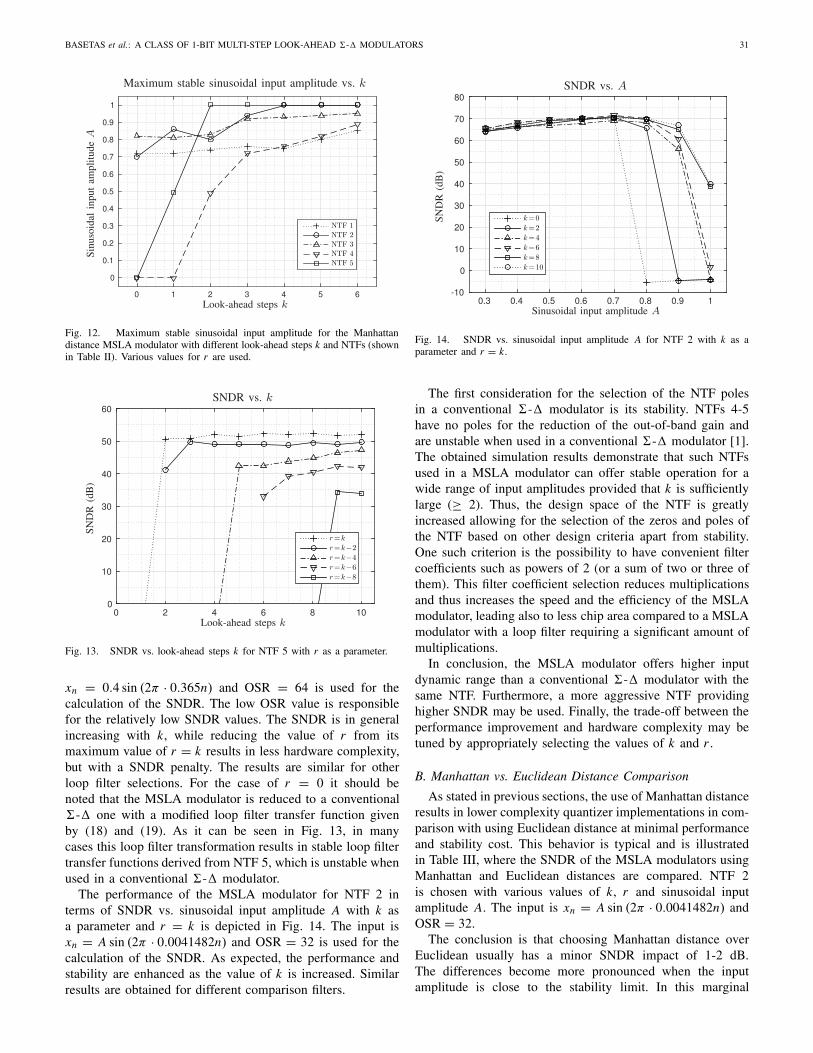
Two kinds of NTFs were chosen; NTFs resulting in stableconventional �-� modulators and NTFs resulting in unstableones. The selection of stable NTFs (NTFs 1-3 in Table II)was based on design guidelines in [1], [21], [22]. The unstableNTFs (4-5 in Table II) have their zeros on the unit circle withpoles at z = 0. Typically NTFs stable in conventional �-�modulators are also stable in MSLA ones. Moreover, as k isincreased they remain stable for higher input amplitudes, whileunstable NTFs in conventional �-� modulators may becomestable. The main advantage of resorting to a look-ahead �-� modulator instead of a conventional one is the possibilityto use more aggressive NTFs in terms of out-of-band gainand thus achieve higher in-band noise attenuation and SNDR(Signal-to-Noise and Distortion Ratio).
The attained stability simulation results are shown in Fig. 12and the corresponding filters are shown in Table II. TheMATLAB simulation uses 2 · 106 input samples. For thelow-pass filters 1-4 xn = A sin (2π · 0.0041482n) was usedas the input and for the band-pass filter 5 it was xn =A sin (2π · 0.365n). The effect of the look-ahead steps k inincreasing the maximum sinusoidal input amplitude for stableoperation is evident. Especially, NTFs 4 and 5, unstable whenused in a conventional �-� modulator loop, i.e., k = 0, resultin stable operation for k ≥ 1 and k ≥ 2 respectively.
In Fig. 13 more simulation results for NTF 5 are presented,demonstrating the impact of k and r on the SNDR (Signal-to-Noise and Distortion Ratio). Here, the input is fixed to
BASETAS et al.: A CLASS OF 1-BIT MULTI-STEP LOOK-AHEAD �-� MODULATORS 31
Fig. 12. Maximum stable sinusoidal input amplitude for the Manhattandistance MSLA modulator with different look-ahead steps k and NTFs (shownin Table II). Various values for r are used.
Fig. 13. SNDR vs. look-ahead steps k for NTF 5 with r as a parameter.
xn = 0.4 sin (2π · 0.365n) and OSR = 64 is used for thecalculation of the SNDR. The low OSR value is responsiblefor the relatively low SNDR values. The SNDR is in generalincreasing with k, while reducing the value of r from itsmaximum value of r = k results in less hardware complexity,but with a SNDR penalty. The results are similar for otherloop filter selections. For the case of r = 0 it should benoted that the MSLA modulator is reduced to a conventional�-� one with a modified loop filter transfer function givenby (18) and (19). As it can be seen in Fig. 13, in manycases this loop filter transformation results in stable loop filtertransfer functions derived from NTF 5, which is unstable whenused in a conventional �-� modulator.
The performance of the MSLA modulator for NTF 2 interms of SNDR vs. sinusoidal input amplitude A with k asa parameter and r = k is depicted in Fig. 14. The input isxn = A sin (2π · 0.0041482n) and OSR = 32 is used for thecalculation of the SNDR. As expected, the performance andstability are enhanced as the value of k is increased. Similarresults are obtained for different comparison filters.
Fig. 14. SNDR vs. sinusoidal input amplitude A for NTF 2 with k as aparameter and r = k.
The first consideration for the selection of the NTF polesin a conventional �-� modulator is its stability. NTFs 4-5have no poles for the reduction of the out-of-band gain andare unstable when used in a conventional �-� modulator [1].The obtained simulation results demonstrate that such NTFsused in a MSLA modulator can offer stable operation for awide range of input amplitudes provided that k is sufficientlylarge (≥ 2). Thus, the design space of the NTF is greatlyincreased allowing for the selection of the zeros and poles ofthe NTF based on other design criteria apart from stability.One such criterion is the possibility to have convenient filtercoefficients such as powers of 2 (or a sum of two or three ofthem). This filter coefficient selection reduces multiplicationsand thus increases the speed and the efficiency of the MSLAmodulator, leading also to less chip area compared to a MSLAmodulator with a loop filter requiring a significant amount ofmultiplications.
In conclusion, the MSLA modulator offers higher inputdynamic range than a conventional �-� modulator with thesame NTF. Furthermore, a more aggressive NTF providinghigher SNDR may be used. Finally, the trade-off between theperformance improvement and hardware complexity may betuned by appropriately selecting the values of k and r .
B. Manhattan vs. Euclidean Distance Comparison
As stated in previous sections, the use of Manhattan distanceresults in lower complexity quantizer implementations in com-parison with using Euclidean distance at minimal performanceand stability cost. This behavior is typical and is illustratedin Table III, where the SNDR of the MSLA modulators usingManhattan and Euclidean distances are compared. NTF 2is chosen with various values of k, r and sinusoidal inputamplitude A. The input is xn = A sin (2π · 0.0041482n) andOSR = 32.
The conclusion is that choosing Manhattan distance overEuclidean usually has a minor SNDR impact of 1-2 dB.The differences become more pronounced when the inputamplitude is close to the stability limit. In this marginal

32 IEEE TRANSACTIONS ON CIRCUITS AND SYSTEMS–I: REGULAR PAPERS, VOL. 64, NO. 1, JANUARY 2017
TABLE III
SNDR COMPARISON OF MANHATTAN AND EUCLIDEAN DISTANCES
case, Manhattan distance might offer increased stability asit is evident in the last row of Table III, i.e., the MSLAmodulator employing Euclidean distance is unstable whereasthe Manhattan distance one maintains stability.
C. Comparison With Other Look-Ahead Algorithms
The benefits of using look-ahead techniques are foundmainly in their increased stability characteristics, thereforeallowing for higher order loop filters, higher SNDR andincreased maximum input amplitudes. Other benefits includetheir lower THD (total harmonic distortion) and noise modula-tion [19]. The observed SNDR of look-ahead modulators withthe same comparison filter (and thus NTF) as a conventional�-� modulator is typically 1-2 dB lower than that of aconventional one for input values in the stable range ofboth modulators. However, this is mitigated by exploiting theincreased stability of look-ahead modulators e.g. use of ahigher order NTF or a NTF with a higher out-of-band gain.
In Section III-C a complexity comparison between variouslook-ahead implementations and the MSLA modulator waspresented, showcasing the reduced relative complexity of theMSLA modulator. Here, we compare the performance ofthese modulators in terms of SNDR and maximum sinusoidalinput amplitude A. The results are summarized in Table IV.The simulation results of the various look-ahead implementa-tions, i.e., pruned look-ahead, efficient trellis and pruned tree(M-algorithm), are taken from [19]. In order to have a faircomparison we have used the same conditions for our sim-ulations. A 5th (or 3rd) order feed-forward loop filter withresonators is used with the configuration SDM2 (or SDM4) asdescribed in Appendix B of [19]. For the SNDR calculationsa −6 dB 1 KHz sine wave is used as the input and OSR = 64is assumed with a sampling frequency of 64 ·44.1 KHz. In allcircumstances 106 output samples are generated. The para-meters of the algorithms were chosen so that their hardwarecomplexity is comparable. This is the reason why the numberof filter output calculations (NoFC) is included in the lastcolumn of Table IV. NoFC is calculated according to Table I.
The MSLA modulator displays similar or betterperformance than other look-ahead algorithms for comparablecomplexity. More specifically, for SDM2 the MSLAmodulator with r = k = 7 or higher outperforms the otherimplementations in terms of SNDR, while for SDM4 the
TABLE IV
COMPARISON OF LOOK-AHEAD ALGORITHMS
selection of r = k = 3 is sufficient to give the MSLAmodulator the performance advantage. A value of r = k = 12is needed for the MSLA modulator in order to exhibit thesame maximum stable sinusoidal amplitude as the pruned treealgorithm with M = 4 and only the pruned tree algorithmwith M = 8 outperforms it, but with the cost of highercomplexity.
D. Output Power Spectra and Applications
In the following test cases MSLA modulators with Man-hattan distance as the cost function are used for the reasonsdiscussed in Section III-B.
1) Low-Pass Modulator With DC Input: A popular appli-cation of �-� modulators with DC input is the generationof the divider control in fractional-N frequency synthesizers.The most common structure used is the 1-1-1 MASH modula-tor [23]. The drawback of MASH is its multi-bit output, whichcomplicates the design of the divider. The MSLA modulatorwith a simple 3rd order low-pass filter offers comparable noiseshaping and stability with 1-bit output.
As a test-case the NTF = (1 − z−1)3 is used witha DC input. An advantage of this NTF is the simplicityof its coefficients, resulting in a multiplier-less, and there-fore fast and power efficient, hardware implementation. Thepower spectrum obtained from 2 · 106 output samples of theMSLA modulator with k = 2 and a DC input of 0.0025is shown Fig. 15. There are some frequency spurs startingat f = 0.0025 fs as it is expected from a DC input valuewhich is a small rational fraction, namely 1/400. However,they can be eliminated when a small random dither is addedto the input [24]. Simulation results also back this claim. Thefrequency and severity of these spurs depend on the DC inputamplitude and on the modulator order. High-order modulatorsexhibit fewer or no spurs due to signal mixing in the higherorder loop filter [1].

BASETAS et al.: A CLASS OF 1-BIT MULTI-STEP LOOK-AHEAD �-� MODULATORS 33
Fig. 15. Power spectrum relative to the carrier of 2 · 106 output samples ofthe low-pass MSLA modulator with k = 2, NTF = (1 − z−1)3 and a DCinput with amplitude 0.0025.
2) Low-Pass Modulator With Sinusoidal Input: Thelow-pass �-� modulator is used in a multitude of appli-cations, with audio being a major one [25], [26]. A purelydigital-to-digital �-� converter is used to generate the1-bit SA-CD (Super Audio CD) bitstream from explicit PCMinput data [19]. Recently, 1-bit low-pass �-� modulatorshave received attention in all-digital transmitter architec-tures [27]–[30].
A NTF with zeros spread across the signal band, forimproved in-band SNR, is chosen for the demonstration ofthe low-pass MSLA modulator output spectrum. The NTF issynthesized using the MATLAB Delta Sigma Toolbox [31]with the following parameters: 7-th order filter, OSR = 16, useof optimized zeros and NTF(∞) = 2. Lee’s rule states thatfor a conventional 1-bit high-order �-� modulator stabilityis guaranteed when NTF(∞) < 1.5 [1]. Indeed, MATLABsimulation indicates that this NTF is unstable when used in aconventional �-� modulator. Due to the low oversamplingratio (OSR), offering a wide fractional signal bandwidth,forcing NTF(∞) < 1.5 results in low noise attenuation in thesignal band. The MSLA modulator with this NTF, r = k = 10and a sinusoidal input signal of amplitude 0.43 is stable. Theoutput spectrum relative to the carrier of 2 ·106 output samplesis shown in Fig. 16. Such a wide signal bandwidth combinedwith such noise attenuation is probably impossible with aconventional 1-bit �-� modulator. To back this claim, thehighest possible NTF(∞) of a EF SDM with a NTF designedwith the same parameters, is found to be NTF(∞) = 1.74. ItsSNDR is estimated at 61.5 dB, while the SNDR of the MSLAmodulator with NTF(∞) = 2 is 68.7 dB.
There are some out-of-band tones at frequencies higher than0.25 fs , but they should be easily eliminated by a subsequentdecimation filter. Simulations with various input amplitudesand frequencies, as well as different loop filters support theassertion that there are no frequency spurs in the signal bandwhen the modulator operates far from overload.
3) Band-Pass Modulator With Sinusoidal Input: Directdigital synthesizers use an accumulator and a sinusoidal look-up table (LUT) to generate a multi-bit digital sinewave.
Fig. 16. Power spectrum relative to the carrier of 2 · 106 output samples ofthe wide-band low-pass MSLA modulator with r = k = 10 and a sinusoidalinput with amplitude 0.43.
Fig. 17. All-digital frequency synthesis using the Multi-Step Look-Aheadband-pass modulator.
The frequency is determined by the frequency control wordfed to the phase accumulator. Finally, the digital stream isconverted to analog via a DAC. Multi-bit DAC non-linearitiesand low effective number of bits (ENOB) introduce numerousspurs. Several works have dealt with techniques to suppressthe spurs [32]–[34].
Alternatively, one can use a band-pass �-� modulator [35]after the sinusoidal LUT for the generation of a 1-bit out-put with the quantization noise shaped out of the signalfrequency band [36]–[41]. This is shown in Fig. 17. TheNTF of this modulator should suppress the noise over awide bandwidth to support signal generation with varyingcarrier frequency. MSLA modulator’s bandwidth advantage isconvenient. Furthermore, converting a 1-bit digital stream toanalog is much less involved compared to a multi-bit one. 1-bitdata conversion, apart from jitter affecting all types of DACs,is subject only to DC offset and gain errors, both harmless forthe output spectrum.
In Fig. 18 the power spectrum relative to the carrierof 2 · 106 output samples of the band-pass MSLA modulatorwith r = k = 7 is shown. A sinusoidal input with frequencyω = 2π ·0.3814 rad/s and amplitude 0.31 was used, while theNTF was designed with the help of the MATLAB Delta SigmaToolbox. The parameters used for the NTF were: 8-th orderfilter, OSR = 16, use of optimized zeros, NTF(∞) = 2 andcentral frequency ω0 = 2π ·0.38 rad/s. Again, the combinationof wide signal bandwidth and in-band noise attenuation is notachievable with a conventional 1-bit �-� modulator. The EFSDM with a NTF designed using the same parameters is stableup to NTF(∞) = 1.69 and achieves a SNDR of 48.7 dB. Theband-pass MSLA modulator with NTF(∞) = 2 exhibits aSNDR of 54.2 dB. Finally, it should be noted that there areno spurs in the whole power spectrum frequency range.

34 IEEE TRANSACTIONS ON CIRCUITS AND SYSTEMS–I: REGULAR PAPERS, VOL. 64, NO. 1, JANUARY 2017
Fig. 18. Power spectrum relative to the carrier of 2 · 106 output samples ofthe band-pass MSLA modulator with r = k = 7 and a sinusoidal input withamplitude 0.31.
Fig. 19. The u j,n computation unit.
V. HARDWARE IMPLEMENTATION ASPECTS
The hardware implementation of the MSLA modulator isbased on the evaluation of (14), while the quantizer inputs u j,n
are given by (13). The hardware complexity depends on thelook-ahead steps k, the quantizer’s input vector length r + 1and the comparison filter.
The proposed architecture is based on a modulardesign, in which the MSLA modulator consists of r + 1two-input filters (L j
0, L j1), which from now on we refer to
as u j,n computation units. In comparison with the brute-force approach of calculating the total cost function for eachpossible output sequence, as it is common in other look-ahead�-� architectures [19], the proposed architecture requiresonly one calculation of vector u per output symbol. Thisfact emphasizes the importance of the analysis presentedin section III.
The block diagram of a u j,n computation unit is shownin Fig. 19. This unit implements (13) and each multiply-and-accumulate (MAC) unit calculates each of the three sumsinvolved. Moreover, the IIR filter unit computes en using thedifference equation corresponding to (16). The quantizer canbe implemented either with combinational logic (e.g. compara-tors) or with a ROM-based LUT. Its mapping function f is
Fig. 20. The proposed hardware architecture of the MSLA modulator withNTF = (1 − z−1)2, k = 1 and r = 1.
determined by the NTF, the number of look-ahead steps k, thevalue of r and the choice of Manhattan or Euclidean distance.Further research is currently performed in order to determinethe best implementation for the quantizer.
The topology of the loop filter implementation has an effecton the number of registers, adders and multipliers required,as well as on the total quantization noise. The most robusttopologies in terms of quantization noise are the cascadeand parallel forms (second-order sections), but the trans-posed form II implementation is more efficient in terms ofrequired hardware [42]. Significant hardware reduction andspeed improvement are possible if the loop filter and the MACunit coefficients are powers of 2 or a sum of powers of 2. Then,all multiplications are reduced to shift operations or two shiftoperations and an addition.
The cascaded integrator with feedback topology seems tobe the optimal structure for a hardware implementation of theloop filter as it offers the possibility to reduce the numberof bits needed after each integrator while it maintains lowdelay [27].
A. FPGA Implementation
As a simple test case, the hardware implementation of theMSLA modulator with NTF = (1 − z−1)2, k = 1 and r = 1is depicted in Fig. 20. Clock signals have been omitted forsimplicity. The output register doubles as the delay elementfor the feedback signal. This modulator is very hardwareefficient, since all multiplications reduce to shift and addoperations. The bit width of the input and the registers hasbeen set to 16 bits with 1 bit output. Further reduction ofthe bit widths along the signal path is possible followingthe design procedure in [27]. The top 4-input adder formsthe u0,n computation unit, i.e., the two-input filter (L0
0, L10),
and the bottom one the u1,n computation unit, i.e., the two-input filter (L0
1, L11). The transfer functions of these filters are
given by (18) and (19) respectively. In our test case we find
BASETAS et al.: A CLASS OF 1-BIT MULTI-STEP LOOK-AHEAD �-� MODULATORS 35
L00(z) = 1/(1 − z−1 + z−2), L1
0(z) = (−2z−1 + z−2)/(1 − z−1 + z−2) for the top filter and L0
1(z) = z/(1 − z−1 + z−2), L1
1(z) = (−3z−1 + 2z−2)/(1 − z−1 + z−2)for the bottom one. The quantizer logic module implementsthe mapping function of Fig. 10a and has two 16-bit inputsand a 1-bit output.
In order to obtain a rough estimation of hardwarerequirements, the modulator has been synthesized for aXilinx Kintex-7 development board using 16-bit fixed-point representation for the modulator signals. The syn-thesis tool reports 7 2-input and 2 3-input 16-bit adders,7 16-bit and 3 1-bit registers in addition to 2 2-input16-bit multiplexers, 1 2-input 15-bit multiplexer and1 2-input 1-bit multiplexer. That is about 1% utilization of theFPGA resources. The maximum clock frequency was reportedat 330 MHz for this FPGA, but IC implementation allows formuch higher clock frequencies [43].
The proposed hardware architecture is suitable for FPGAand IC CMOS implementations. The superior speed of anIC implementation is of great importance as the OSR canbe increased, and thus the noise attenuation in the pass-bandcan be even higher. In any case, the hardware overhead ofthe MSLA modulator is low, which means it can be easilyand cheaply incorporated in a larger mixed-signal or all-digitaldesign. Furthermore, the 1-bit output eliminates the need for amulti-bit DAC, leading to inherently linear, all-digital designs.
VI. CONCLUSIONS
The MSLA modulator, which is a modification of the1-bit EF SDM taking into account future input samples,has been introduced. It exhibits superior stability character-istics, allowing for higher input dynamic range and moreaggressive NTFs resulting in higher SNDR than conventional1-bit �-� modulators. Moreover, comparison of the MSLAmodulator with other look-ahead algorithms highlights itsperformance advantage and low relative complexity, whichenables real-time operation. The MSLA modulator has beenanalyzed mathematically and shown to be equivalent to anumber of conventional �-� modulators in parallel, sharinga common multi-input 1-bit quantizer. The simulation resultshave illustrated the advantages of the MSLA modulator in avariety of applications. Finally, a hardware architecture hasbeen proposed and a specific FPGA implementation has beenpresented, showing that moderate values of k and r do notimpose a significant increase in hardware complexity whencompared to a conventional 1-bit �-� modulator.
APPENDIX ANOTATION OVERVIEW
G Comparison filter transfer function.b Comparison filter numerator coefficients.a Comparison filter denominator coefficients.� Comparison filter numerator order.m Comparison filter denominator order.k Number of look-ahead steps.r + 1 Number of partial costs involved in the
calculation of the total cost.
{x} The MSLA modulator input sequence.{y} The MSLA modulator output sequence.{e} Comparison filter G output sequence.{v} The trial feedback sequence.j The j -th look-ahead sample (k − r ≤ j ≤ k).Sj,n Partial cost associated with the j -th
look-ahead sample at time instant n.c j,i Coefficients associated with MSLA modulator
loop filters(
L0j (z) , L1
j (z))
.
d j,i Coefficients associated with MSLA modulator
loop filters(
L0j (z) , L1
j (z))
.
u j,n The output of the loop filter(
L j0 (z) , L j
1 (z))
.
u(uk−r,n , uk−r+1,n , . . . , uk,n
)
v (v0, v1, . . . , vk)D (v) The total cost function.f (u) The MSLA quantizer mapping function.L0
j The transfer function of the MSLAmodulator’s j -th loop filter X input.
L1j The transfer function of the MSLA
modulator’s j -th loop filter Y input.NTF The NTF of the EF SDM (Fig. 1).STF The STF of the EF SDM (Fig. 1).NTFMSLA The NTF of the MSLA modulator.STFMSLA The STF of the MSLA modulator.
APPENDIX B
This appendix demonstrates the derivation of (12) and (13)from (8). In the following analysis it is assumed that �, m > j .The same equations are still valid if � ≤ j or m ≤ j by settingbi = 0 for i > � and ai = 0 for i > m respectively.
The first step is to express every en+ j , k − r ≤ j ≤ k interms of the inputs xi , the previous outputs yi , the previousfilter G outputs en−i , i ≥ 0 and a linear combination ofv0, v1, . . ., v j−1. This is accomplished by application of thefilter difference equation (9) for every en+i , 0 < i ≤ j . Usingmatrix notation this is written
en+ jn+1 = Bx xn+ j−1
n+1−� −Bvv j−10 −Byyn−1
n+1−�−Aen+ j−1n+1−m (28)
where the vector notation qi+pi = [qi+p, qi+p−1, . . ., qi ] is
used, v j−10 = [v j−1, v j−2, . . ., v0] and
Bv =
⎡
⎢⎢⎢⎢⎢⎣
b1 b2 b3 · · · b j
0 b1 b2 · · · b j−1...
. . .. . .
. . ....
0 · · · 0 b1 b20 0 · · · 0 b1
⎤
⎥⎥⎥⎥⎥⎦
(29)
By =
⎡
⎢⎢⎢⎢⎢⎣
b j+1 b j+2 · · · b� 0 0 · · · 0b j b j+1 · · · b�−1 b� 0 · · · 0...
......
......
. . .. . .
...b3 b4 · · · b�− j+2 b�− j+3 · · · b� 0b2 b3 · · · b�− j+1 b�− j+2 · · · b�−1 b�
⎤
⎥⎥⎥⎥⎥⎦
(30)
Bx = [Bv By
](31)

36 IEEE TRANSACTIONS ON CIRCUITS AND SYSTEMS–I: REGULAR PAPERS, VOL. 64, NO. 1, JANUARY 2017
with Bv a j × j matrix, By a j × (� − 1) matrix and Bx aj ×( j + � − 1) matrix. In order to solve for en+ j the last termof (28) is rewritten as
Aen+ j−1n+1−m = A1en+ j
n+1 + A2enn+1−m (32)
where
A1 =
⎡
⎢⎢⎢⎢⎢⎢⎢⎣
0 a1 a2 · · · a j−2 a j−10 0 a1 a2 · · · a j−2...
.... . .
. . .. . .
...0 0 · · · 0 a1 a20 0 0 · · · 0 a10 0 0 · · · 0 0
⎤
⎥⎥⎥⎥⎥⎥⎥⎦
(33)
A2 =
⎡
⎢⎢⎢⎢⎢⎣
a j a j+1 · · · am 0 0 · · · 0a j−1 a j · · · am−1 am 0 · · · 0
......
......
.... . .
. . ....
a2 a3 · · · am− j+2 am− j+3 · · · am 0a1 a2 · · · am− j+1 am− j+2 · · · am−1 am
⎤
⎥⎥⎥⎥⎥⎦
(34)
with A1 a j × j matrix and A2 a j × m matrix. Combining(28) with (32) we get
en+ jn+1 = (I + A1)
−1(
Bx xn+ j−1n+1−� − Bvv j−1
0 − Byyn−1n+1−�
− A2enn+1−m
). (35)
Matrix I + A1 is upper unitriangular Toeplitz [44]. Its inverseis also upper unitriangular Toeplitz, i.e.
M � (I + A1)−1 =
⎡
⎢⎢⎢⎢⎢⎢⎢⎣
1 β1 β2 · · · β j−2 β j−10 1 β1 β2 · · · β j−2...
. . .. . .
. . .. . .
...0 · · · 0 1 β1 β20 0 · · · 0 1 β10 0 0 · · · 0 1
⎤
⎥⎥⎥⎥⎥⎥⎥⎦
(36)where β1 = −a1 and
βi = −ai −i−1∑
p=1
ai−pβp (37)
for 2 ≤ i ≤ j − 1. Therefore en+ j is derived from the firstrow of (35) which is written as
en+ j = β0 j−1
[Bv
(xn+ j−1
n − v j−10
)
+ By
(xn−1
n+1−l − yn−1n+1−l
)− A2en
n+1−m
](38)
where β0 j−1 = [β0, β1. . ., β j−1] is a row vector with
β0 ≡ 1. In (38) we used Bx = [Bv By
]. Performing the matrix
multiplications gives
en+ j =j∑
i=1
c j,i(xn+ j−i − v j−i
)
+j+�−1∑
i= j+1
c j,i(xn+ j−i − yn+ j−i
) +m−1∑
i=0
d j,i en−i
(39)
where coefficients c j,i , 1 ≤ i ≤ j + � − 1 form the elementsof row vector β0
j−1Bx and coefficients d j,i , 0 ≤ i ≤ m − 1form the elements of row vector −β0
j−1A2. Defining βi = 0for i ≥ j is convenient for writing them explicitly as
c j,i ={∑i
p=1 βi−pbp, 1 ≤ i ≤ �∑�
p=1 βi−pbp, � < i ≤ j + � − 1(40)
and
d j,i ={
− ∑ j−1p=0 βpai+ j−p, 0 ≤ i ≤ m − j
− ∑m−i−1p=0 βp+i+ j−mam−p, m − j < i ≤ m − 1.
(41)
In addition, we define for all j c j,0 = 1. The substitution ofen+ j as given by (39) into (10) yields the equivalent expressionof Sj,n(v0, v1, . . ., v j ) given in (12).
ACKNOWLEDGEMENT
The authors would like to thank the Editor-in-Chief,the Associate Editor, and the anonymous reviewers for theirvaluable comments and constructive feedback.
REFERENCES
[1] R. Schreier and G. C. Temes, Understanding Delta-Sigma DataConverters, S. V. Kartalopoulos, Ed. New York, NY, USA: Wiley, 2005.
[2] K. Hosseini and M. P. Kennedy, “Maximum sequence length MASHdigital delta-sigma modulators,” IEEE Trans. Circuits Syst. I, Reg.Papers, vol. 54, no. 12, pp. 2628–2638, Dec. 2007.
[3] R. F. Cordeiro, A. S. R. Oliveira, J. Vieira, and N. V. Silva, “Gigasampletime-interleaved delta-sigma modulator for FPGA-based all-digital trans-mitters,” in Proc. IEEE 17th Euromicro Conf. Digit. Syst. Des. (DSD),Aug. 2014, pp. 222–227.
[4] M. Helaoui, S. Hatami, R. Negra, and F. M. Ghannouchi, “A novelarchitecture of delta-sigma modulator enabling all-digital multibandmultistandard RF transmitters design,” IEEE Trans. Circuits Syst. II,Express Briefs, vol. 55, no. 11, pp. 1129–1133, Nov. 2008.
[5] R. B. Staszewski, “State-of-the-art and future directions of high-performance all-digital frequency synthesis in nanometer CMOS,” IEEETrans. Circuits Syst. I, Reg. Papers, vol. 58, no. 7, pp. 1497–1510,Jul. 2011.
[6] Y. L. Tang, J. G. Ma, and F. Xiong, “Implementation of sigma deltamodulator for fractional-N frequency synthesis,” in Proc. Proc. IEEEInt. Symp. Integr. Circuits, Sep. 2007, pp. 497–499.
[7] R. B. Staszewski and P. T. Balsara, “Phase-domain all-digitalphase-locked loop,” IEEE Trans. Circuits Syst. II, Express Briefs, vol. 52,no. 3, pp. 159–163, Mar. 2005.
[8] G. I. Bourdopoulos, A. Pnevmatikakis, V. Anastassopoulos, andT. L. Deliyannis, Delta-Sigma Modulators: Modeling, Design and Appli-cations. London, U.K.: Imperial College Press, 2003.
[9] P. Kiss, J. Arias, D. Li, and V. Boccuzzi, “Stable high-order delta-sigmadigital-to-analog converters,” IEEE Trans. Circuits Syst. I, Reg. Papers,vol. 51, no. 1, pp. 200–205, Jan. 2004.
[10] V. Mladenov, H. Hegt, and A. van Roermund, “Stability analysis ofhigh order sigma-delta modulators,” in Proc. Eur. Conf. Circuit TheoryDesign (ECCTD), Espoo, Finland, Aug. 2001, pp. 313–316.
[11] S. Hein and A. Zakhor, “On the stability of sigma delta modulators,”IEEE Trans. Signal Process., vol. 41, no. 7, pp. 2322–2348, Jul. 1993.
[12] S. H. Ardalan and J. J. Paulos, “An analysis of nonlinear behaviorin delta-sigma modulators,” IEEE Trans. Circuits Syst., vol. 34, no. 6,pp. 593–603, Jun. 1987.
[13] L. Risbo, “Sigma-delta modulators-stability analysis and optimization,”Ph.D. dissertation, Tech. Univ. Denmark, Lyngby, Denmark, Jun. 1994.[Online]. Available: http://orbit.dtu.dk/services/downloadRegister/5274022/Binder1.pdf
[14] A. K. Gupta and O. M. Collins, “Viterbi decoding and sigma-delta mod-ulation,” in Proc. IEEE Int. Symp. Inf. Theory, Lausanne, Switzerland,Jun./Jul. 2002, p. 292.
[15] A. K. Gupta and O. M. Collins, “A new interpretation and extensionof sigma delta modulation,” in Proc. IEEE Int. Symp. Inf. Theory,Washington, DC, USA, Jun. 2001, p. 194.

BASETAS et al.: A CLASS OF 1-BIT MULTI-STEP LOOK-AHEAD �-� MODULATORS 37
[16] R. Gopalan and O. M. Collins, “On an optimum algorithm for waveformsynthesis and its applications to digital transmitters,” in Proc. Proc. IEEEWireless Commun. Netw. Conf. (WCNC), Mar. 2005, pp. 1108–1113.
[17] R. Gopalan and O. M. Collins, “An optimization approach to single-bitquantization,” IEEE Trans. Circuits Syst. I, Reg. Papers, vol. 56, no. 12,pp. 2655–2668, Dec. 2009.
[18] A. Okabe, B. Boots, K. Sugihara, and S. N. Chiu, Spatial Tessellations:Concepts and Applications of Voronoi Diagrams, 2nd ed. New York,NY, USA: Wiley, 2000.
[19] E. Janssen and A. van Roermund, Look-Ahead Based Sigma-DeltaModulation. New York, NY, USA: Springer 2011.
[20] J. Venkataraman and O. Collins, “An all-digital transmitter witha 1-bit DAC,” IEEE Trans. Commun., vol. 55, no. 10, pp. 1951–1962,Oct. 2007.
[21] R. Schreier, “An empirical study of high-order single-bit delta-sigmamodulators,” IEEE Trans. Circuits Syst. II, Analog Digit. Signal Process.,vol. 40, no. 8, pp. 461–466, Aug. 1993.
[22] S. R. Norsworthy, R. Schreier, and G. C. Temes, Eds., Delta-SigmaData Converters: Theory, Design, and Simulation. Piscataway, NJ, USA:IEEE Press, 1997.
[23] K. Hosseini and M. P. Kennedy, “Mathematical analysis of digitalMASH delta-sigma modulators for fractional-n frequency synthesis,”Ph.D. dissertation, Res. Microelectron. Electron., 2006, pp. 309–312.
[24] W. Chou and R. M. Gray, “Dithering and its effects on sigma-delta andmultistage sigma-delta modulation,” IEEE Trans. Inf. Theory, vol. 37,no. 3, pp. 500–513, May 1991.
[25] E. Dallago, G. De Leo, and G. Sassone, “A current-mode power sigma-delta modulator for audio applications,” IEEE Trans. Ind. Electron.,vol. 52, no. 1, pp. 236–242, Feb. 2005.
[26] S. Rabii and B. A. Wooley, “A 1.8-V digital-audio sigma-delta modu-lator in 0.8-μm CMOS,” IEEE J. Solid-State Circuits, vol. 32, no. 6,pp. 783–796, Jun. 1997.
[27] R. Huang, N. Lotze, and Y. Manoli, “On design a high speed sigmadelta DAC modulator for a digital communication transceiver on chip,”in Proc. IEEE 11th Euromicro Conf. Digit. Syst. Design Archit., MethodsTools, 2008, pp. 53–60.
[28] A. Frappe, A. Flament, B. Stefanelli, A. Kaiser, and A. Cathelin, “Anall-digital RF signal generator using high-speed �� modulators,” IEEEJ. Solid-State Circuits, vol. 44, no. 10, pp. 2722–2732, Oct. 2009.
[29] N. V. Silva, A. S. R. Oliveira, U. Gustavsson, and N. B. Carvalho,“A dynamically reconfigurable architecture enabling all-digital transmis-sion for cognitive radios,” in Proc. IEEE Radio Wireless Symp. (RWS),Jan. 2012, pp. 1–4.
[30] C. Basetas and P. P. Sotiriadis, “Single-bit-output all-digital frequencysynthesis using multi-step look-ahead bandpass � − � modulator-likequantization processing,” in Proc. IEEE Int. Freq. Control Symp. Eur.Freq. Time Forum, Denver, CO, USA, Apr. 2015, pp. 448–451.
[31] R. Schreier. (Dec. 2011). Delta Sigma Toolbox. [Online]. Available:http://www.mathworks.com/matlabcentral/fileexchange/19-delta-sigma-toolbox
[32] P. P. Sotiriadis and K. Galanopoulos, “Direct all-digital frequencysynthesis techniques, spurs suppression, and deterministic jitter cor-rection,” IEEE Trans. Circuits Syst. I, Reg. Papers, vol. 59, no. 5,pp. 958–968, May 2012.
[33] J. Vankka, “Spur reduction techniques in sine output direct digitalsynthesis,” in Proc. IEEE Int. Freq. Control Symp., Honolulu, HI, USA,Jun. 1996, pp. 951–959.
[34] V. S. Reinhardt, “Spur reduction techniques in direct digital synthesiz-ers,” in Proc. IEEE Int. Freq. Control Symp., Salt Lake City, UT, USA,Jun. 1993, pp. 230–241.
[35] R. Schreier, “Noise-shaped coding,” Ph.D. dissertation, Univ. Toronto,Toronto, ON, Canada, 1991.
[36] K. Galanopoulos, C. Basetas, and P. P. Sotiriadis, “Delta-sigma modula-tion techniques to reduce noise and spurs in all-digital RF transmitters,”in Proc. IEEE Int. Freq. Control Symp., Taipei, Taiwan, May 2014,pp. 1–3.
[37] R. Schreier and M. Snelgrove, “Bandpass sigma-delta modulation,”Electron. Lett., vol. 25, no. 23, pp. 1560–1561, Nov. 1989.
[38] J. Sommarek, J. Vankka, J. Ketola, J. Lindeberg, and K. Halonen,“A digital modulator with bandpass delta-sigma modulator,” in Proc.30th Eur. Solid-State Circuits Conf., Sep. 2004, pp. 159–162.
[39] P. P. Sotiriadis, “Spurs-free single-bit-output all-digital frequency syn-thesizers with forward and feedback spurs and noise cancellation,”IEEE Trans. Circuits Syst. I, Reg. Papers, vol. 63, no. 5, pp. 567–576,May 2016.
[40] P. P. Sotiriadis, “Single-bit all digital frequency synthesis using homo-dyne sigma-delta modulation,” IEEE Trans. Ultrason., Ferroelect., Freq.Control, to be published.
[41] P. P. Sotiriadis, “All digital frequency synthesis based on newsigma-delta modulation architectures,” in Proc. Proc. IEEE Int. Freq.Control Symp. Eur. Freq. Time Forum, Denver, CO, USA, Apr. 2015,pp. 667–671.
[42] A. V. Oppenheim and R. W. Schafer, Discrete-Time Signal Processing,2nd ed. Englewood Cliffs, NJ, USA: Prentice-Hall, 1999.
[43] C. Basetas and P. P. Sotiriadis, “Hardware implementation aspectsof multi-step look-ahead �� modulation-like architectures for all-digital frequency synthesis applications,” in Proc. Proc. IEEE Int. Freq.Control Symp. Eur. Freq. Time Forum, Denver, CO, USA, Apr. 2015,pp. 452–455.
[44] R. A. Horn and C. R. Johnson, Matrix Analysis. Cambridge, U.K.:Cambridge Univ. Press, 1990.
Charis Basetas received the M.S. degree in elec-trical and computer engineering from the Univer-sity of Patras, Greece, in 2007. Currently he isworking toward the Ph.D. degree at the NationalTechnical University of Athens, Greece, workingunder the supervision of Prof. Sotiriadis. He is incharge of two undergraduate courses and acts asan advisor for several diploma theses. His mainresearch interests include digital VLSI design, digitalsignal processing, computer arithmetic and wirelesscommunication systems. He is the author of several
conference papers and one journal article, while he is a regular reviewer formany IEEE publications. He is an IEEE student member and a member ofthe Technical Chamber of Greece.
Thanasis Orfanos (S’16) received the M.S. degreein electrical and computer engineering from theNational Technical University of Athens, Greece, in2015. His thesis was on the development and opti-mization of MSLA FPGA implementations and wassupervised by Prof. Sotiriadis. His major researchfields and interests include digital signal processing,FPGA programming, as well as advanced techniquesfor automatic control systems. He also serves as areviewer for a number of IEEE publications.
Paul P. Sotiriadis (SM’09) received the Diplomadegree in electrical and computer engineering fromthe National Technical University of Athens, Greece,the M.S. degree in electrical engineering fromStanford University, Stanford, CA, USA, and thePh.D. degree in electrical engineering and computerscience from the Massachusetts Institute of Tech-nology, Cambridge, MA, USA, in 2002. In 2002,he joined the Johns Hopkins University as AssistantProfessor of Electrical and Computer Engineering.In 2012, he joined the faculty of the Electrical and
Computer Engineering Department of the National Technical University ofAthens, Greece. He has authored and coauthored more than 90 technicalpapers in IEEE journals and conferences, holds one patent, has severalpatents pending, and has contributed chapters to technical books. His researchinterests include design, optimization, and mathematical modeling of analogand mixed-signal circuits, RF and microwave circuits, advanced frequencysynthesis, biomedical instrumentation, and interconnect networks in deep-submicrometer technologies. He has led several projects in these fields fundedby U.S. organizations and has collaborations with industry and national labs.He has received several awards, including a Best Paper Award in the IEEEInternational Symp. on Circuits and Systems 2007, a Best Paper Award in theIEEE International Frequency Control Symp. 2012 and the 2012 Guillemin-Cauer Award from the IEEE Circuits and Systems Society. Dr. Sotiriadisis an Associate Editor of the IEEE TRANSACTIONS ON CIRCUITS AND
SYSTEMS—PART I and the IEEE Sensors Journal, has served as an AssociateEditor of the IEEE TRANSACTIONS ON CIRCUITS AND SYSTEMS—PART IIfrom 2005 to 2010 and has been a member of technical committees of manyconferences. He regularly reviews for many IEEE transactions and conferencesand serves on proposal review panels.


![IEEE TRANSACTIONS ON CIRCUITS AND SYSTEMS …ssl.kaist.ac.kr/2007/data/journal/[2010_TCSVT]JooYoungKim.pdf · IEEE TRANSACTIONS ON CIRCUITS AND SYSTEMS FOR VIDEO TECHNOLOGY, VOL.](https://static.fdocuments.us/doc/165x107/5aa3c0047f8b9a84398ec6d7/ieee-transactions-on-circuits-and-systems-sslkaistackr2007datajournal2010tcsvt.jpg)