©2004 Brooks/Cole FIGURES FOR CHAPTER 9 MULTIPLEXERS, DECODERS, AND PROGRAMMABLE LOGIC DEVICES...
44
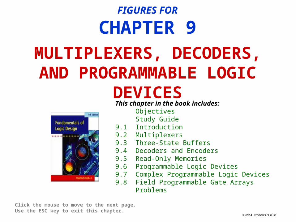
©2004 Brooks/Cole FIGURES FOR CHAPTER 9 MULTIPLEXERS, DECODERS, AND PROGRAMMABLE LOGIC DEVICES Click the mouse to move to the next page. Use the ESC key to exit this chapter. This chapter in the book includes: Objectives Study Guide 9.1 Introduction 9.2 Multiplexers 9.3 Three-State Buffers 9.4 Decoders and Encoders 9.5 Read-Only Memories 9.6 Programmable Logic Devices 9.7 Complex Programmable Logic Devices 9.8 Field Programmable Gate Arrays Problems
-
Upload
cornelius-mathews -
Category
Documents
-
view
221 -
download
0
Transcript of ©2004 Brooks/Cole FIGURES FOR CHAPTER 9 MULTIPLEXERS, DECODERS, AND PROGRAMMABLE LOGIC DEVICES...
©2004 Brooks/Cole
FIGURES FOR
CHAPTER 9MULTIPLEXERS, DECODERS, AND PROGRAMMABLE LOGIC DEVICES
Click the mouse to move to the next page.Use the ESC key to exit this chapter.
This chapter in the book includes:ObjectivesStudy Guide
9.1 Introduction9.2 Multiplexers9.3 Three-State Buffers9.4 Decoders and Encoders9.5 Read-Only Memories9.6 Programmable Logic Devices9.7 Complex Programmable Logic Devices9.8 Field Programmable Gate Arrays
Problems

©2004 Brooks/Cole
Figure 9-1: 2-to-1 Multiplexer and Switch Analog
©2004 Brooks/Cole
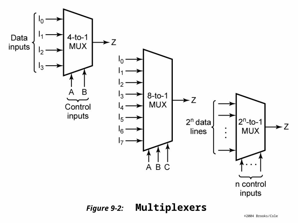
Figure 9-2: Multiplexers

©2004 Brooks/Cole
Figure 9-3: Logic Diagram for 8-to-1 MUX

©2004 Brooks/Cole
Figure 9-4: Quad Multiplexer Used to Select Data
©2004 Brooks/Cole
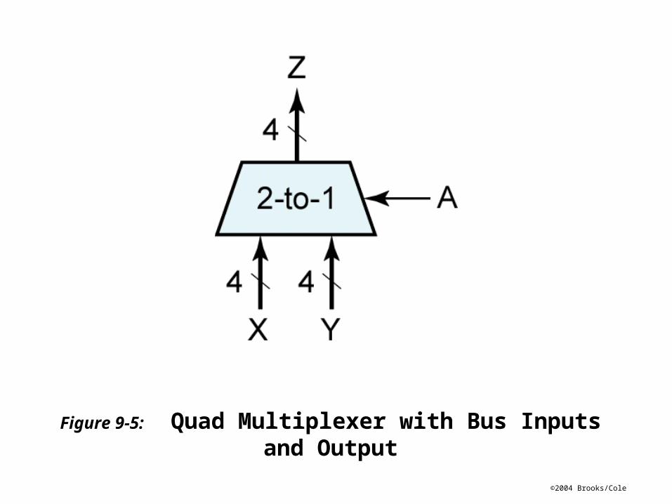
Figure 9-5: Quad Multiplexer with Bus Inputs and Output

©2004 Brooks/Cole
Figure 9-6: Gate Circuit with Added Buffer
©2004 Brooks/Cole
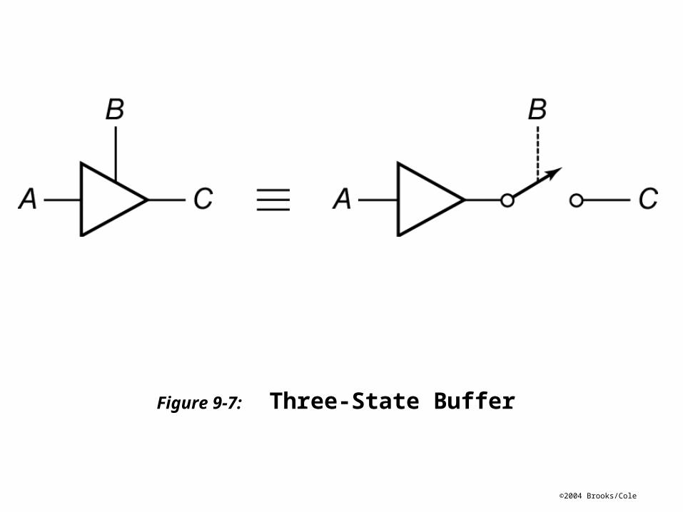
Figure 9-7: Three-State Buffer
©2004 Brooks/Cole
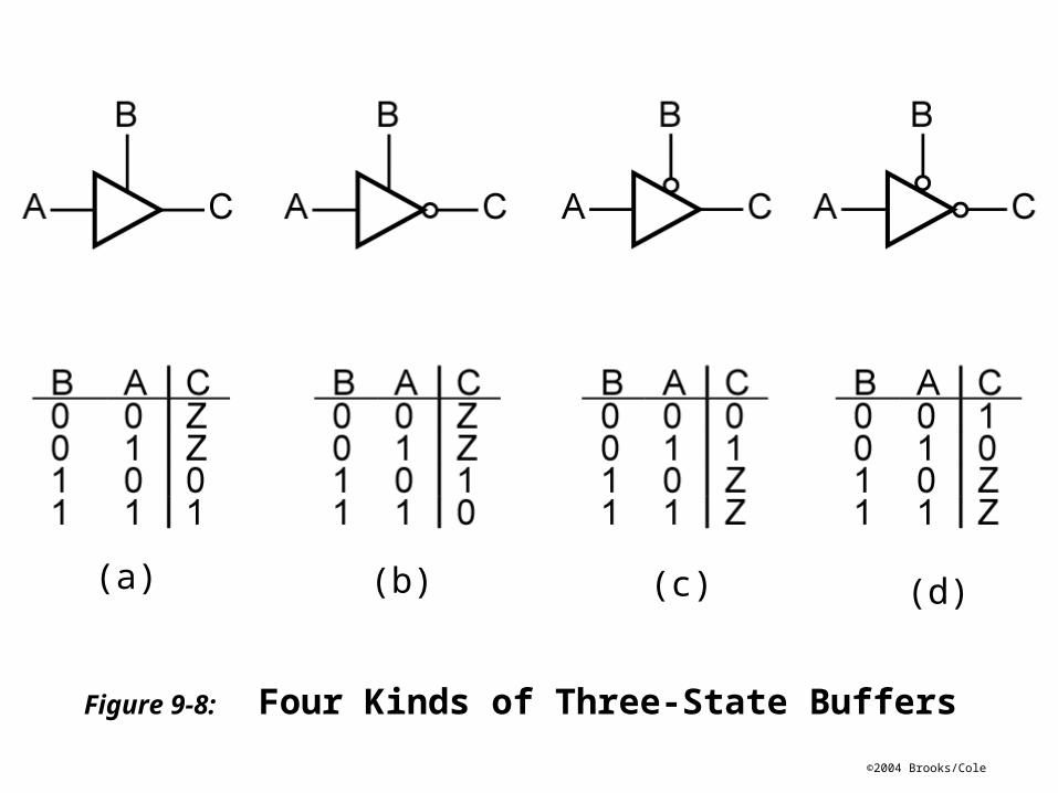
Figure 9-8: Four Kinds of Three-State Buffers
(a) (b) (c) (d)
©2004 Brooks/Cole
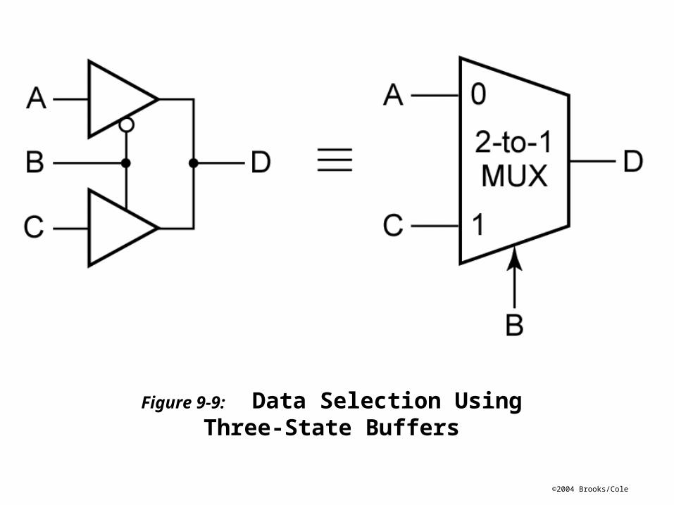
Figure 9-9: Data Selection UsingThree-State Buffers
©2004 Brooks/Cole
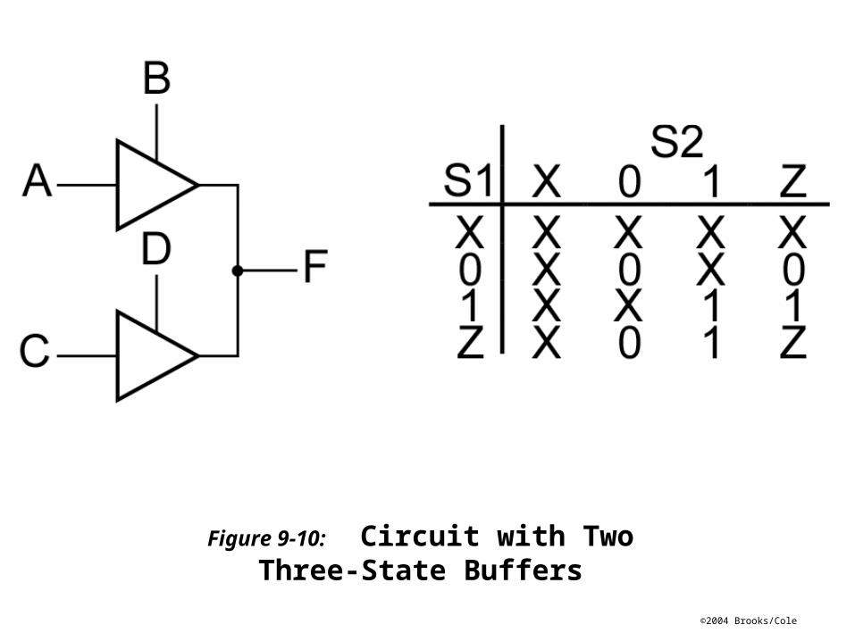
Figure 9-10: Circuit with TwoThree-State Buffers
©2004 Brooks/Cole
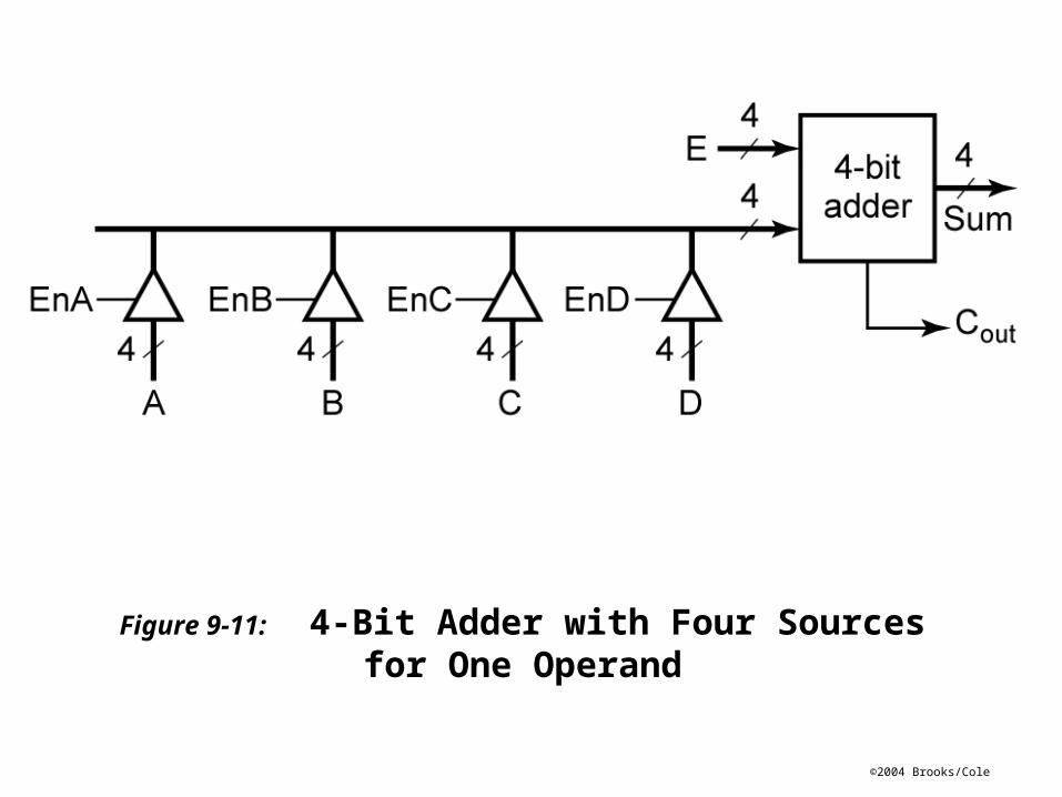
Figure 9-11: 4-Bit Adder with Four Sources for One Operand
©2004 Brooks/Cole
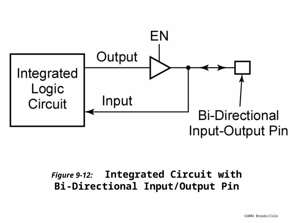
Figure 9-12: Integrated Circuit withBi-Directional Input/Output Pin
©2004 Brooks/Cole
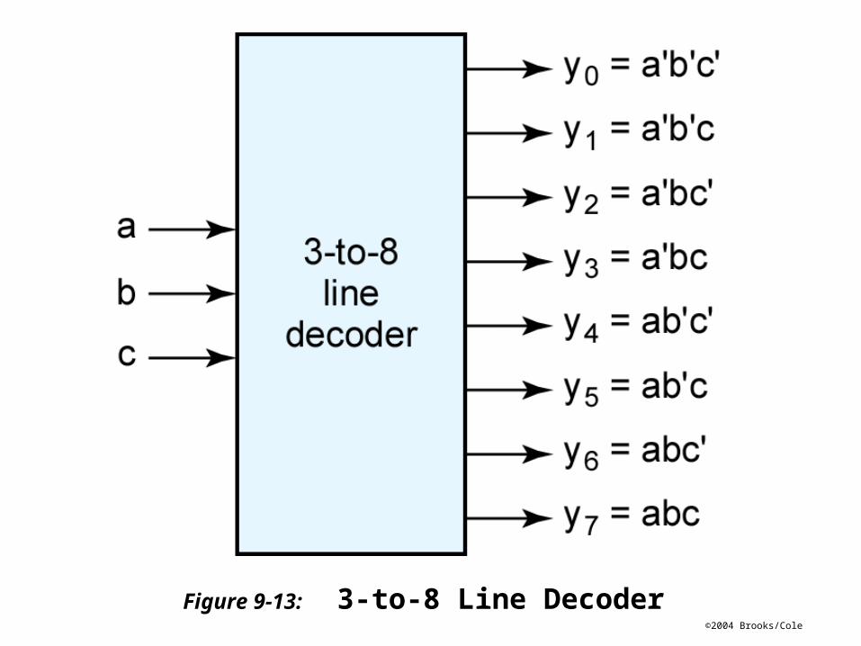
Figure 9-13: 3-to-8 Line Decoder
©2004 Brooks/Cole
Figure 9-13: 3-to-8 Line Decoder
©2004 Brooks/Cole
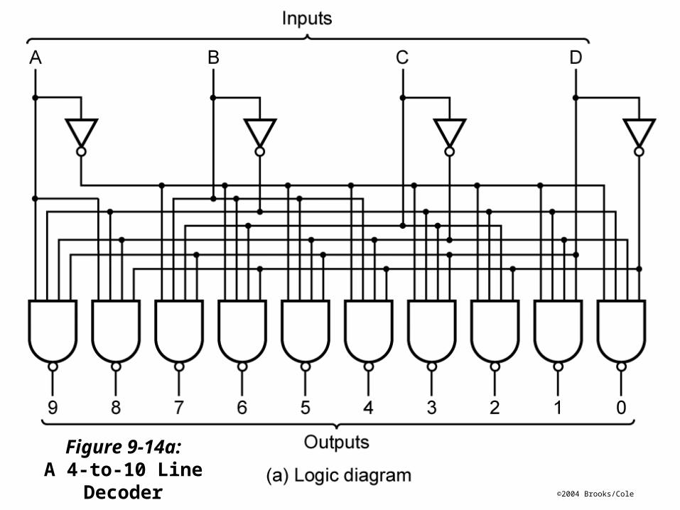
Figure 9-14a:A 4-to-10 Line
Decoder
©2004 Brooks/Cole
(b) Block diagramFigure 9-14b:
A 4-to-10 Line Decoder

©2004 Brooks/Cole
(c) Truth TableFigure 9-14c:A 4-to-10 Line Decoder
©2004 Brooks/Cole
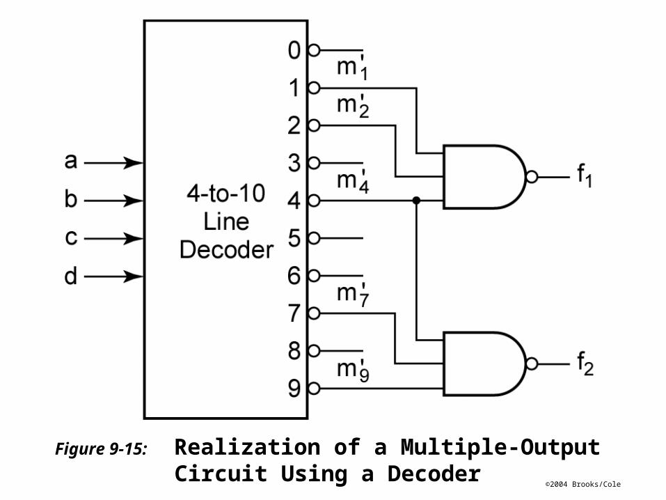
Figure 9-15: Realization of a Multiple-Output Circuit Using a Decoder
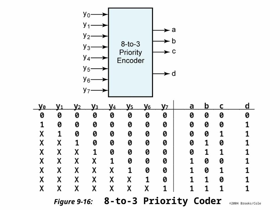
©2004 Brooks/ColeFigure 9-16: 8-to-3 Priority Coder

©2004 Brooks/ColeFigure 9-17: An 8-Word x 4-Bit ROM
(a) Block diagram
©2004 Brooks/Cole
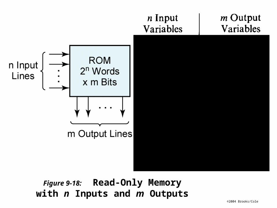
Figure 9-18: Read-Only Memory with n Inputs and m Outputs
©2004 Brooks/Cole
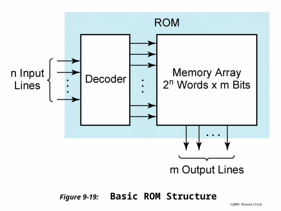
Figure 9-19: Basic ROM Structure

©2004 Brooks/Cole
Figure 9-20: An 8-Word x 4-Bit ROM

©2004 Brooks/Cole
Figure 9-21: Equivalent OR Gate for F0

©2004 Brooks/ColeFigure 9-22: Hexadecimal to ASCII Code Converter

©2004 Brooks/Cole
Figure 9-22: Hexadecimal to ASCII Code Converter

©2004 Brooks/Cole
Figure 9-23: ROM Realization of Code Converter

©2004 Brooks/Cole
Figure 9-24: Programmable Logic Array Structure
©2004 Brooks/Cole
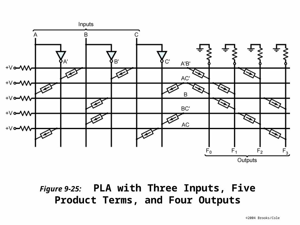
Figure 9-25: PLA with Three Inputs, Five Product Terms, and Four Outputs

©2004 Brooks/Cole
Figure 9-26: AND-OR Array Equivalent to Figure 9-25
©2004 Brooks/Cole
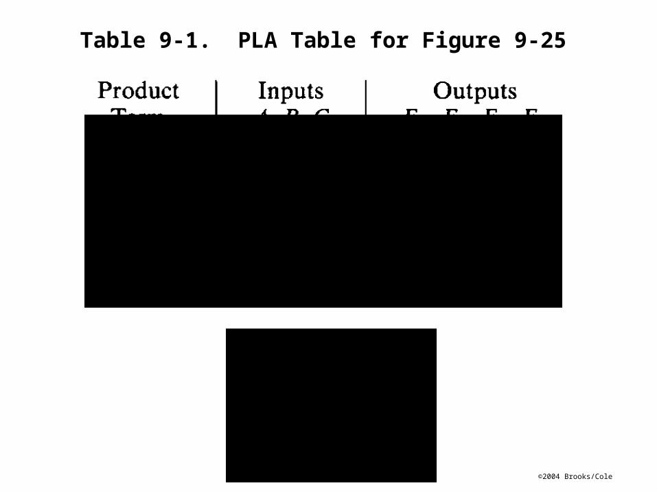
Table 9-1. PLA Table for Figure 9-25

©2004 Brooks/ColeFigure 9-27b: PLA Realization of Equations
(a) PLA table

©2004 Brooks/Cole
Section 9.6, p. 245
Buffer logically equivalent to
©2004 Brooks/Cole
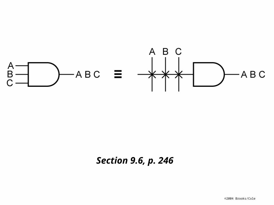
Section 9.6, p. 246

©2004 Brooks/Cole
Figure 9-28:PAL Segment
©2004 Brooks/Cole
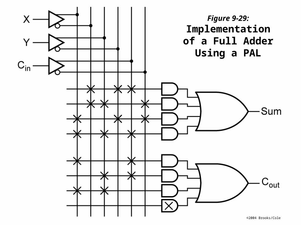
Figure 9-29:
Implementationof a Full Adder
Using a PAL

©2004 Brooks/Cole
Figure 9-30: Architecture of Xilinx XCR3064XL CPLD (Figure based on figures and text owned by Xilinx, Inc., Courtesy of Xilinx, Inc. © Xilinx, Inc.
1999-2003. All rights reserved.)
©2004 Brooks/Cole
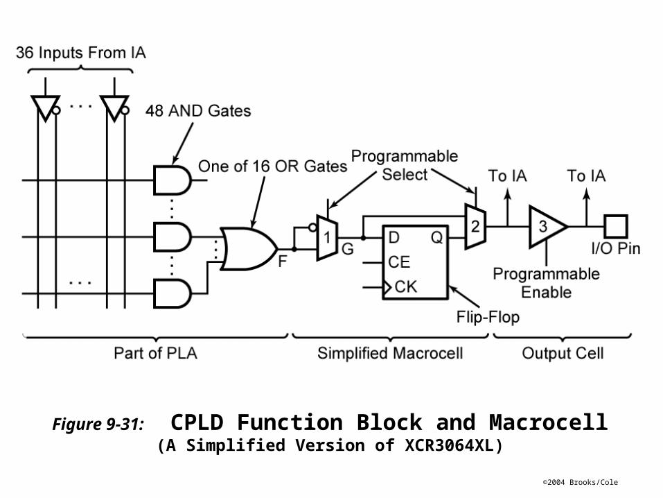
Figure 9-31: CPLD Function Block and Macrocell (A Simplified Version of XCR3064XL)
©2004 Brooks/Cole
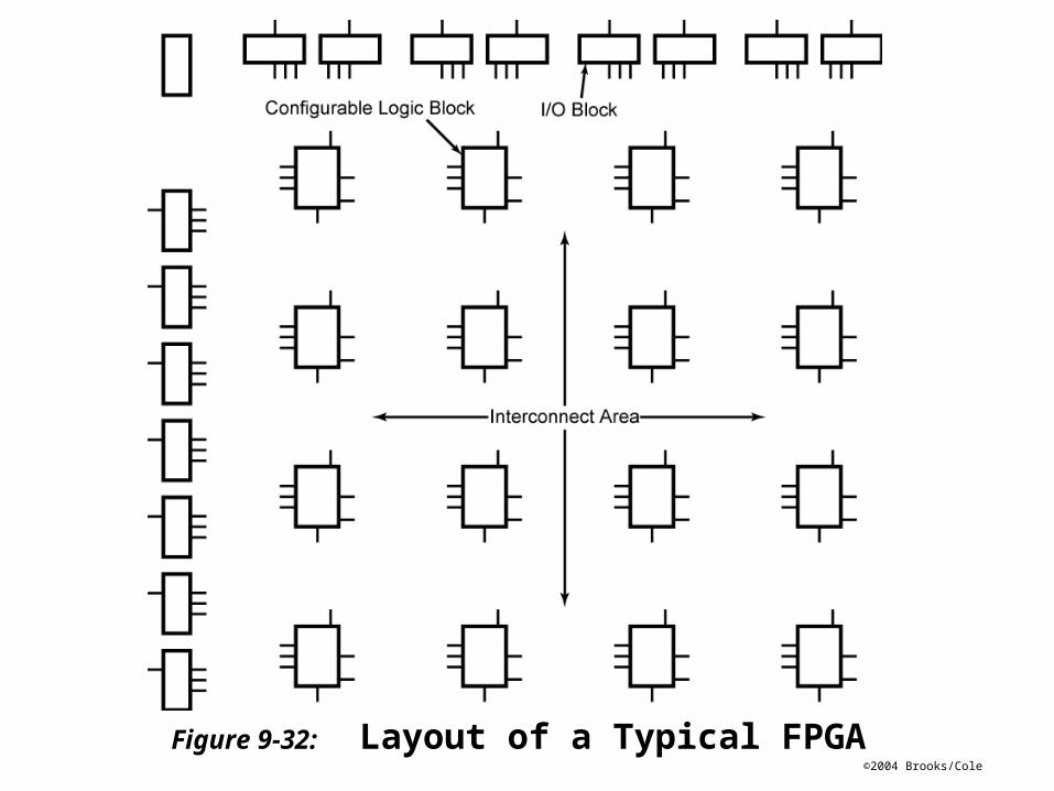
Figure 9-32: Layout of a Typical FPGA
©2004 Brooks/Cole
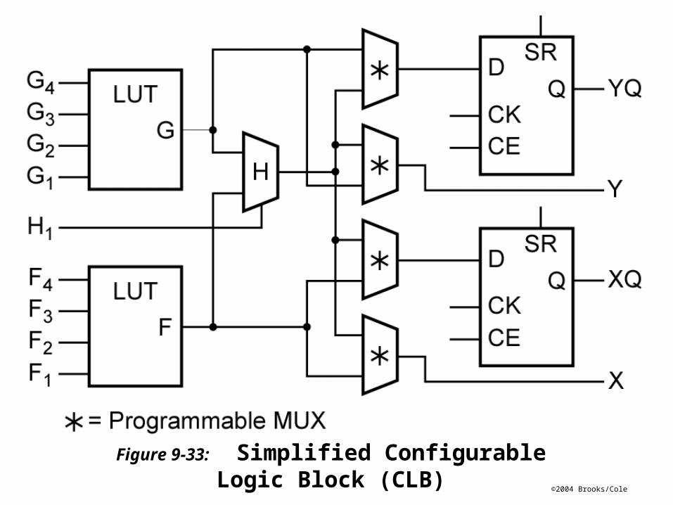
Figure 9-33: Simplified ConfigurableLogic Block (CLB)

©2004 Brooks/Cole
Figure 9-34:
Implementation of a Lookup Table (LUT)
©2004 Brooks/Cole
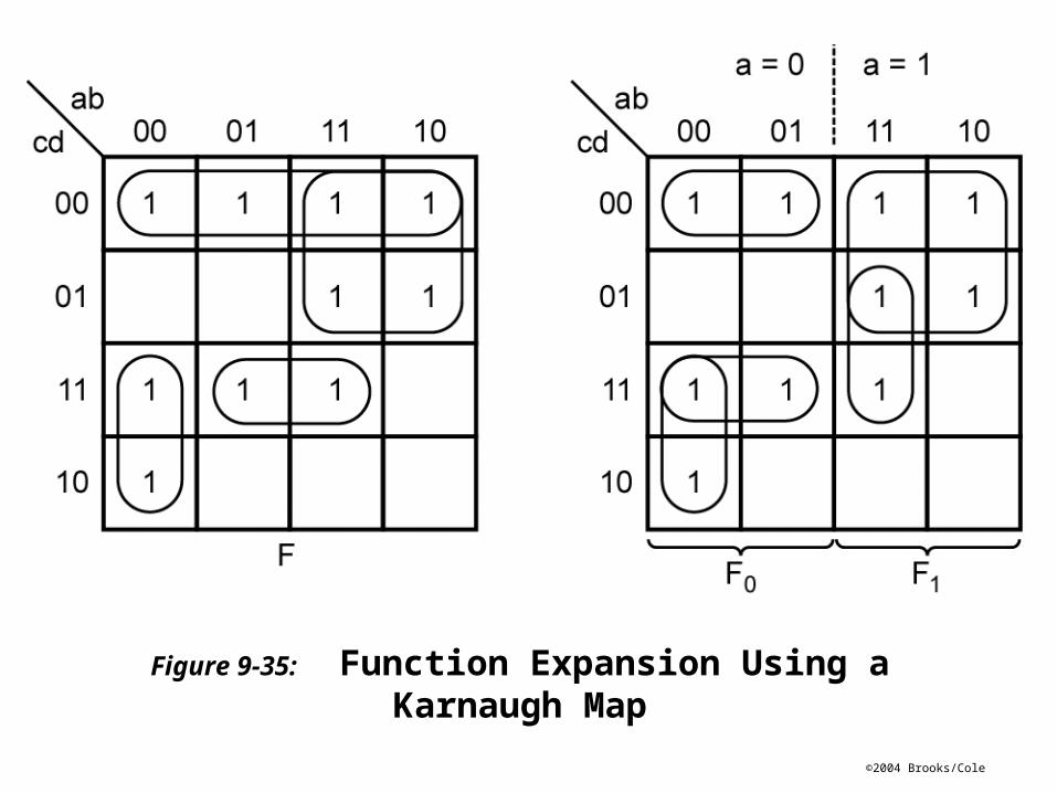
Figure 9-35: Function Expansion Using a Karnaugh Map
©2004 Brooks/Cole
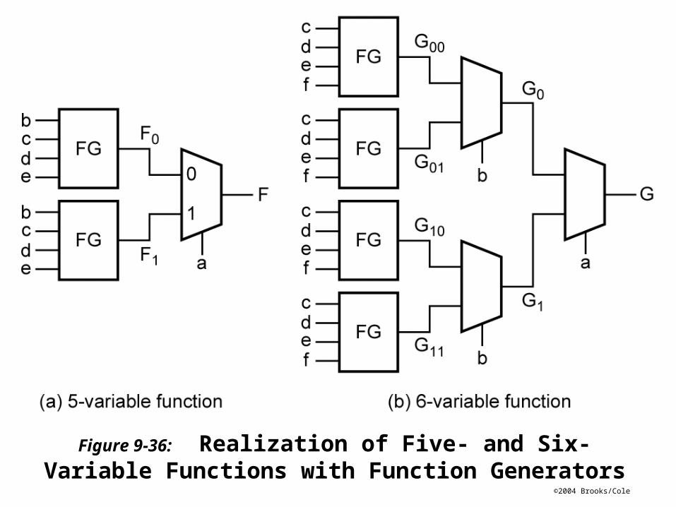
Figure 9-36: Realization of Five- and Six-Variable Functions with Function Generators