


Languages
Pages
Legal


Digital Integrated Circuits © Prentice Hall 1995InverterInverter
THE INVERTERS

Digital Integrated Circuits © Prentice Hall 1995InverterInverter
DIGITAL GATESFundamental Parameters
l Functionalityl Reliability, Robustnessl Areal Performance
» Speed (delay)» Power Consumption» Energy

Digital Integrated Circuits © Prentice Hall 1995InverterInverter
Noise in Digital Integrated Circuits
VDDv(t)
i(t)
(a) Inductive coupling (b) Capacitive coupling (c) Power and ground
noise

Digital Integrated Circuits © Prentice Hall 1995InverterInverter
DC Operation:Voltage Transfer Characteristic
V(x)
V(y)
VOH
VOL
VM
VOHVOL
fV(y)=V(x)
Switching Threshold
Nominal Voltage Levels
V(y)V(x)

Digital Integrated Circuits © Prentice Hall 1995InverterInverter
Mapping between analog and digital signals
"1"
"0"
VOHVIH
VIL
VOL
UndefinedRegion
V(x)
V(y)
VOH
VOL
VIHV
IL
Slope = -1
Slope = -1
Digital Integrated Circuits © Prentice Hall 1995InverterInverter
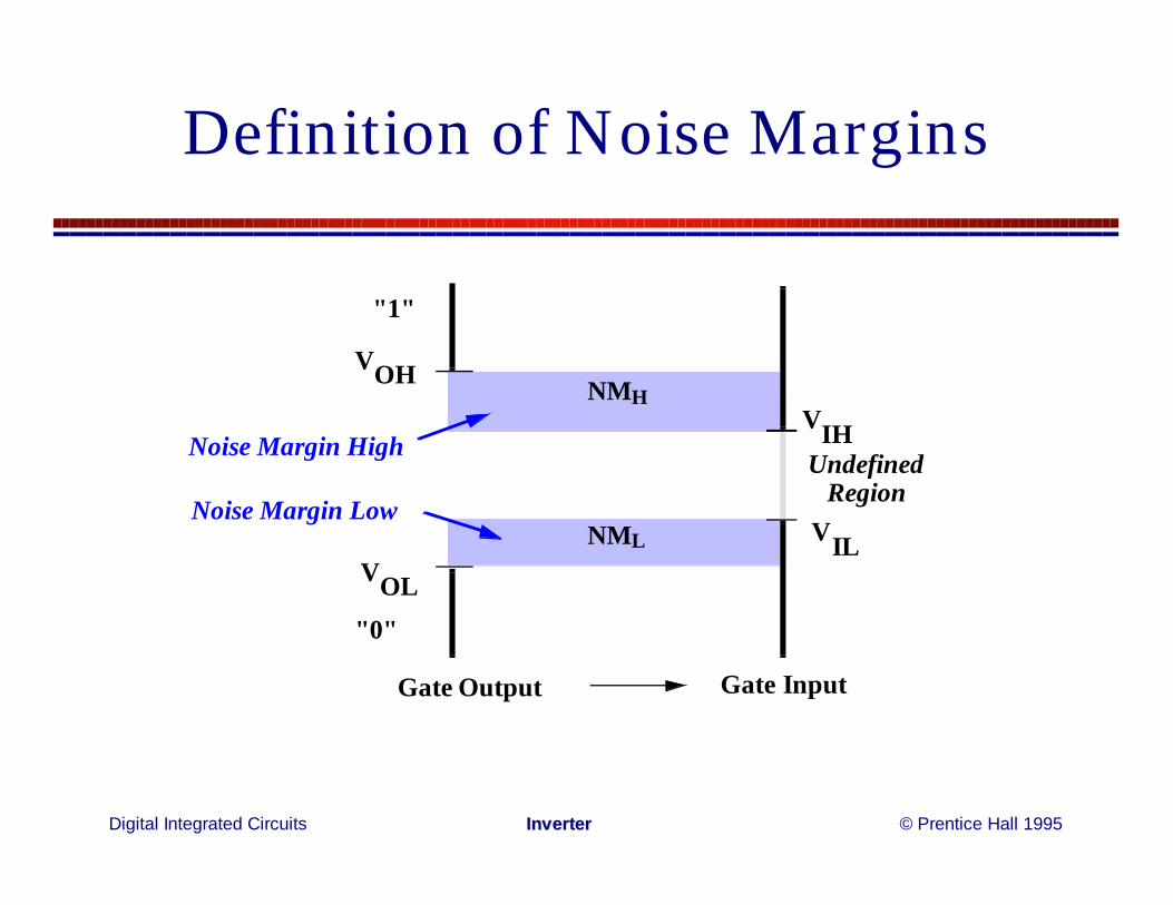
Definition of Noise Margins
VIH
VIL
UndefinedRegion
"1"
"0"
VOH
VOL
NMH
NML
Gate Output Gate Input
Noise Margin High
Noise Margin Low

Digital Integrated Circuits © Prentice Hall 1995InverterInverter
The Regenerative Property
(a) A chain of inverters.
v0, v2, ...
v1, v3, ... v1, v3, ...
v0, v2, ...
(b) Regenerative gate
f(v)
finv(v)
finv(v)
f(v)
(c) Non-regenerative gate
v0 v1 v2 v3 v4 v5 v6
...

Digital Integrated Circuits © Prentice Hall 1995InverterInverter
Fan-in and Fan-out
N
M
(a) Fan-out N
(b) Fan-in M

Digital Integrated Circuits © Prentice Hall 1995InverterInverter
The Ideal Gate
Vin
Vout
g=− ∞
Ri = ∞
Ro = 0

Digital Integrated Circuits © Prentice Hall 1995InverterInverter
VTC of Real Inverter
0.0 1.0 2.0 3.0 4.0 5.0Vin (V)
1.0
2.0
3.0
4.0
5.0
Vou
t (V
)
VMNMH
NML
Digital Integrated Circuits © Prentice Hall 1995InverterInverter
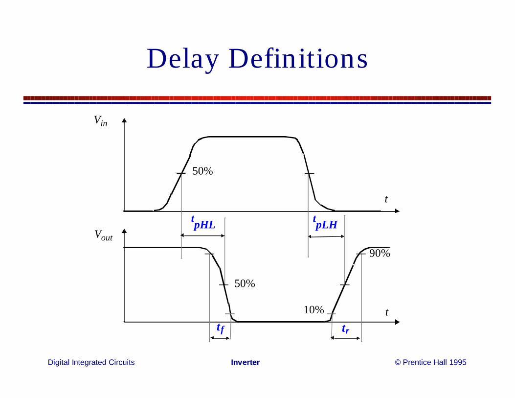
Delay Definitions
tpHL tpLH
t
t
Vin
Vout
50%
50%
tr
10%
90%
tf
Digital Integrated Circuits © Prentice Hall 1995InverterInverter
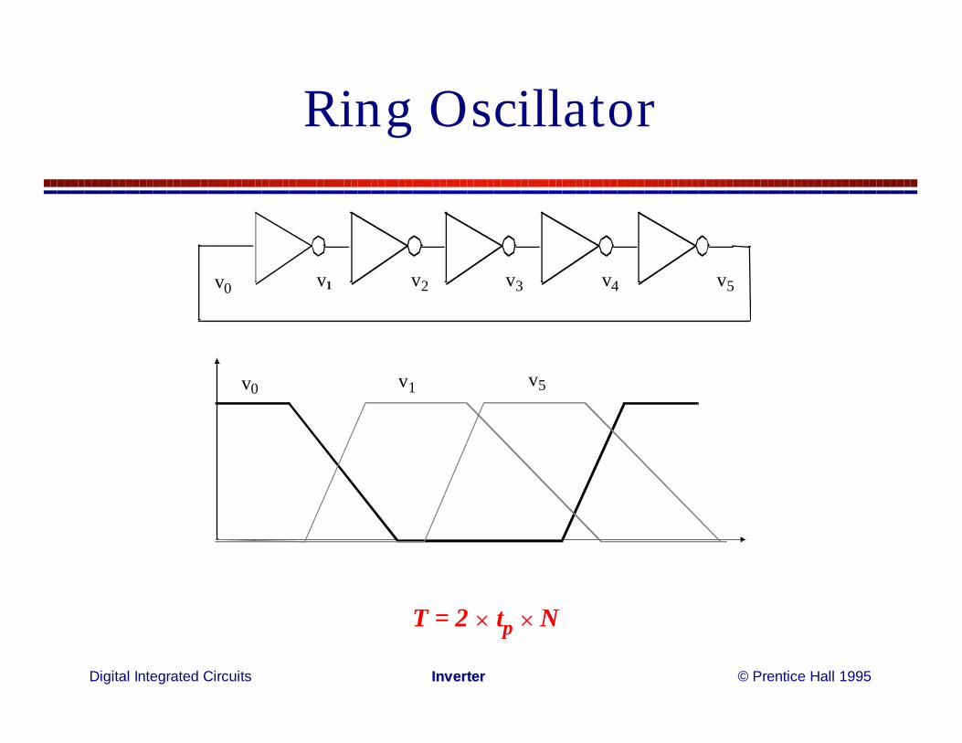
Ring Oscillator
v0 v1 v2 v3 v4 v5
v0 v1 v5
T = 2 × tp × N

Digital Integrated Circuits © Prentice Hall 1995InverterInverter
Power Dissipation
Digital Integrated Circuits © Prentice Hall 1995InverterInverter
CMOS INVERTER

Digital Integrated Circuits © Prentice Hall 1995InverterInverter
The CMOS Inverter:A First Glance
VDD
Vin Vout
CL

Digital Integrated Circuits © Prentice Hall 1995InverterInverter
CMOS Inverters
Polysilicon
InOut
Metal1
VDD
GND
PMOS
NMOS
1.2 µm=2λ

Digital Integrated Circuits © Prentice Hall 1995InverterInverter
Switch Model of CMOS Transistor
Ron
|VGS | < |VT| |VGS| > |VT|
|VGS|

Digital Integrated Circuits © Prentice Hall 1995InverterInverter
CMOS Inverter: Steady State Response
VDD VDD
VoutVout
Vin = VDD Vin = 0
Ron
Ron
VOH = VDD
VOL= 0
VM = Ronp) f(Ronn,
Digital Integrated Circuits © Prentice Hall 1995InverterInverter
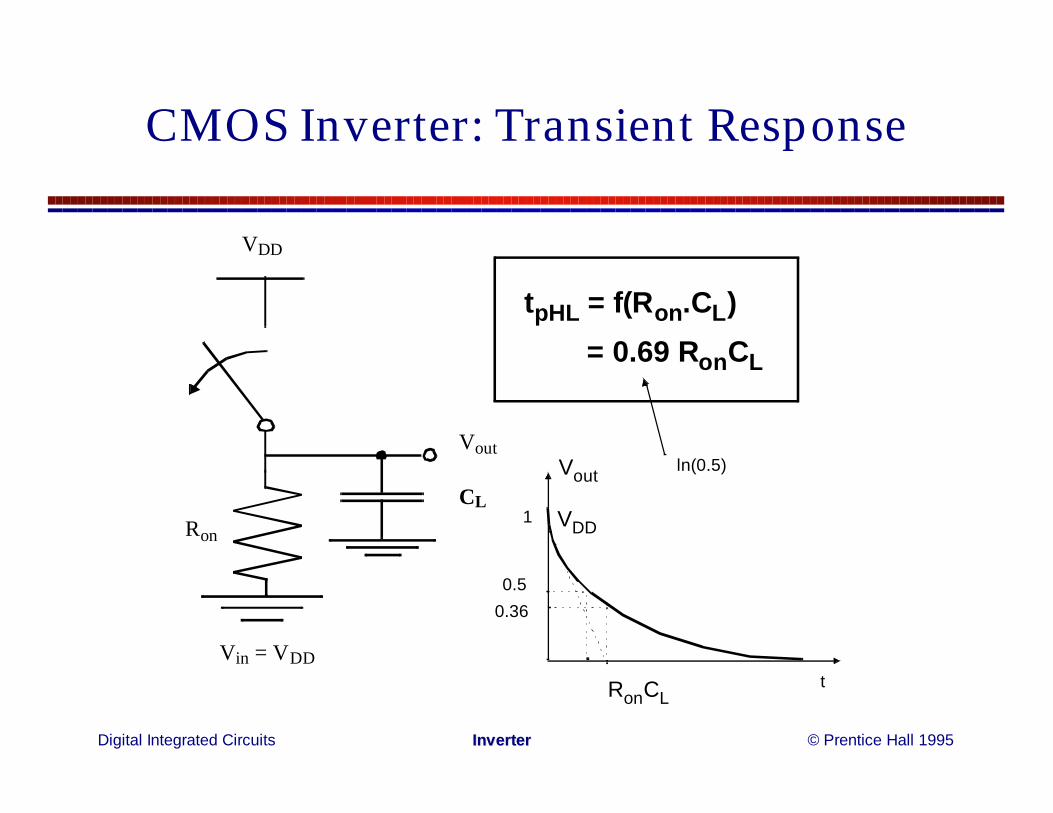
CMOS Inverter: Transient Response
VDD
Vout
Vin = VDD
Ron
CL
tpHL = f(Ron.CL)
= 0.69 RonCL
t
Vout
VDD
RonCL
1
0.5
ln(0.5)
0.36

Digital Integrated Circuits © Prentice Hall 1995InverterInverter
CMOS Properties
l Full rail-to-rail swingl Symmetrical VTCl Propagation delay function of load
capacitance and resistance of transistorsl No static power dissipationl Direct path current during switching

Digital Integrated Circuits © Prentice Hall 1995InverterInverter
Voltage TransferCharacteristic

Digital Integrated Circuits © Prentice Hall 1995InverterInverter
PMOS Load Lines
VDSp
IDp
VGSp=-5
VGSp=-2VDSp
IDnVin=0
Vin=3
Vout
IDnVin=0
Vin=3
Vin = VDD-VGSpIDn = - IDp
Vout = VDD-VDSp
Vout
IDnVin = VDD-VGSpIDn = - IDp
Vout = VDD-VDSp
Digital Integrated Circuits © Prentice Hall 1995InverterInverter
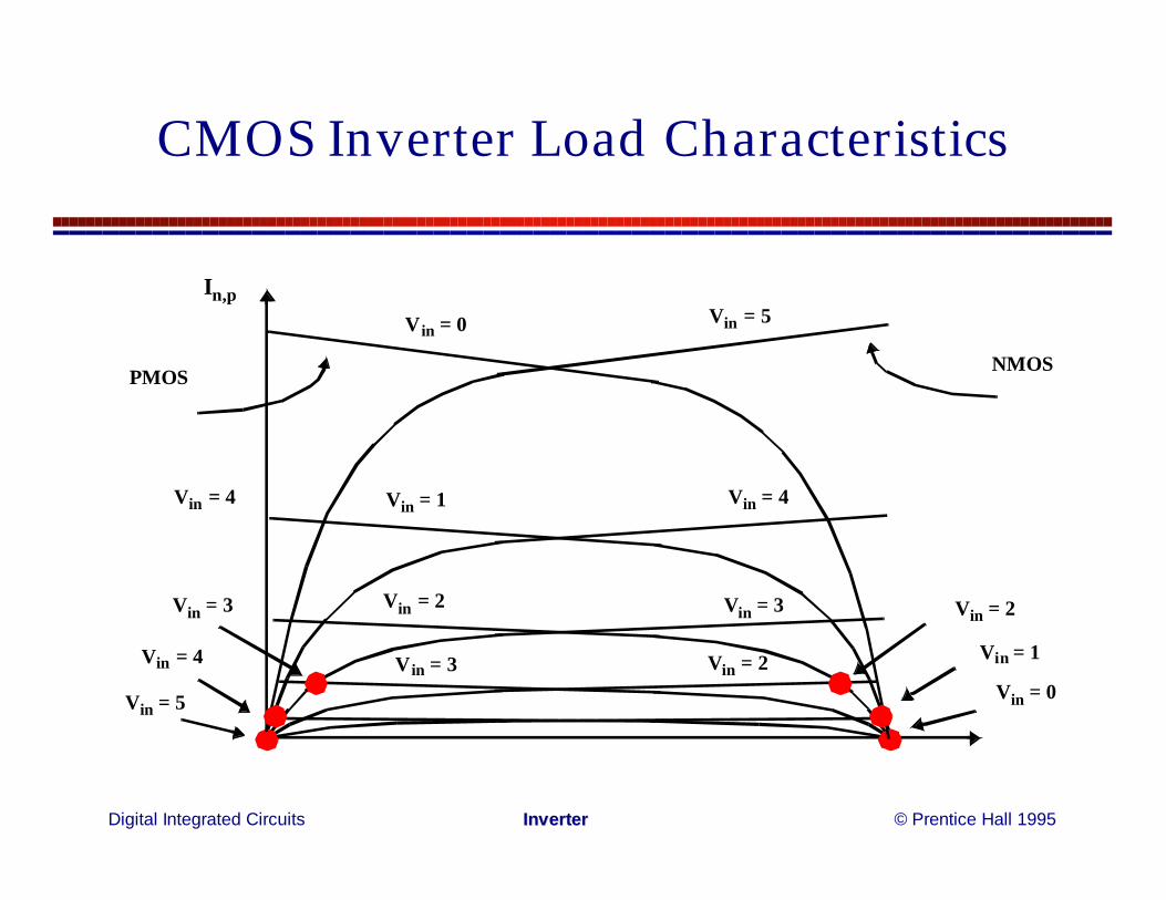
CMOS Inverter Load Characteristics
In,pVin = 5
Vin = 4
Vin = 3
V in = 0
Vin = 1
Vin = 2
NMOSPMOS
Vin = 0
Vin = 1
Vin = 2Vin = 3
Vin = 4
Vin = 4
Vin = 5
Vin = 2V in = 3

Digital Integrated Circuits © Prentice Hall 1995InverterInverter
CMOS Inverter VTC
Vout
Vin1 2 3 4 5
12
34
5
NMOS linPMOS off
NMOS satPMOS sat
NMOS offPMOS lin
NMOS satPMOS lin
NMOS linPMOS sat

Digital Integrated Circuits © Prentice Hall 1995InverterInverter
Simulated VTC
0.0 1.0 2.0 3.0 4.0 5.0Vin (V)
0.0
2.0
4.0
Vou
t (V
)

Digital Integrated Circuits © Prentice Hall 1995InverterInverter
Gate Switching Threshold
0.1 0.3 1.0 3.2 10.01.0
2.0
3.0
4.0
kp/kn
VM
Digital Integrated Circuits © Prentice Hall 1995InverterInverter
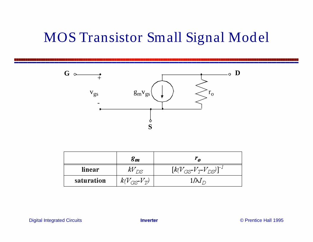
MOS Transistor Small Signal Model
rogmvgsvgs
+
-
S
DG

Digital Integrated Circuits © Prentice Hall 1995InverterInverter
Determining VIH and VIL

Digital Integrated Circuits © Prentice Hall 1995InverterInverter
Propagation Delay

Digital Integrated Circuits © Prentice Hall 1995InverterInverter
CMOS Inverter: Transient Response
VDD
Vout
Vin = VDD
Ron
CL
tpHL = f(Ron.CL)
= 0.69 RonCL
t
Vout
VDD
RonCL
1
0.5
ln(0.5)
0.36
Digital Integrated Circuits © Prentice Hall 1995InverterInverter
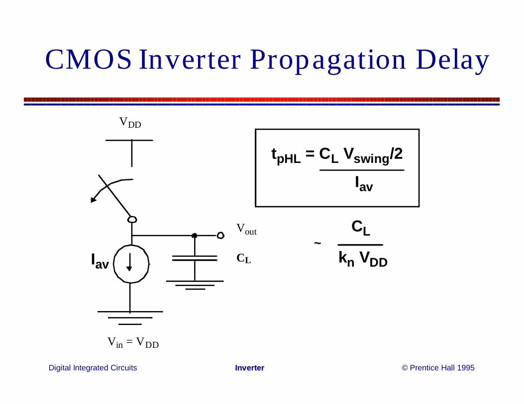
CMOS Inverter Propagation Delay
VDD
Vout
Vin = VDD
CLIav
tpHL = CL Vswing/2
Iav
CL
kn VDD~
Digital Integrated Circuits © Prentice Hall 1995InverterInverter
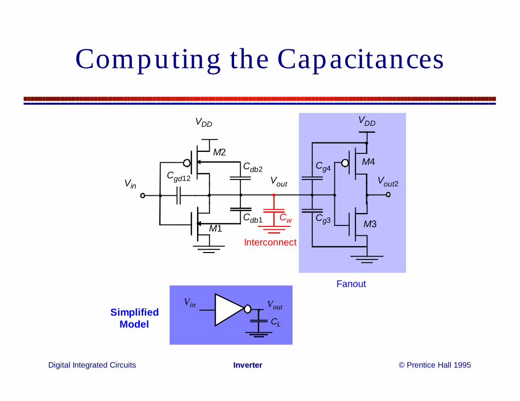
Computing the Capacitances
VDD VDD
VinVout
M1
M2
M3
M4Cdb2
Cdb1
Cgd12
Cw
Cg4
Cg3
Vout2
Fanout
Interconnect
VoutVin
CLSimplified
Model

Digital Integrated Circuits © Prentice Hall 1995InverterInverter
CMOS Inverters
Polysilicon
InOut
Metal1
VDD
GND
PMOS
NMOS
1.2 µm=2λ

Digital Integrated Circuits © Prentice Hall 1995InverterInverter
The Miller Effect
Vin
M1
Cgd1Vout
∆V
∆V
Vin
M1
Vout ∆V
∆V
2Cgd1
“A capacitor experiencing identical but opposite voltage swings at both its terminals can be replaced by a capacitor to ground, whose value is two times the original value.”

Digital Integrated Circuits © Prentice Hall 1995InverterInverter
Computing the Capacitances

Digital Integrated Circuits © Prentice Hall 1995InverterInverter
Impact of Rise Time on Delayt p
HL(n
sec)
0.35
0.3
0.25
0.2
0.15
trise (nsec)10.80.60.40.20

Digital Integrated Circuits © Prentice Hall 1995InverterInverter
Delay as a function of VDD
0
4
8
12
16
20
24
28
2.00 4.001.00 5.003.00
Nor
mal
ized
Del
ay
VDD (V)

Digital Integrated Circuits © Prentice Hall 1995InverterInverter
Where Does Power Go in CMOS?
• Dynamic Power Consumption
• Short Circuit Currents
• Leakage
Charging and Discharging Capacitors
Short Circuit Path between Supply Rails during Switching
Leaking diodes and transistors

Digital Integrated Circuits © Prentice Hall 1995InverterInverter
Dynamic Power Dissipation
Energy/transition = CL * Vdd2
Power = Energy/transition * f = CL * Vdd2 * f
Need to reduce CL, Vdd, and f to reduce power.
Vin Vout
CL
Vdd
Not a function of transistor sizes!

Digital Integrated Circuits © Prentice Hall 1995InverterInverter
Impact ofTechnology Scaling

Digital Integrated Circuits © Prentice Hall 1995InverterInverter
Technology Evolution
Digital Integrated Circuits © Prentice Hall 1995InverterInverter
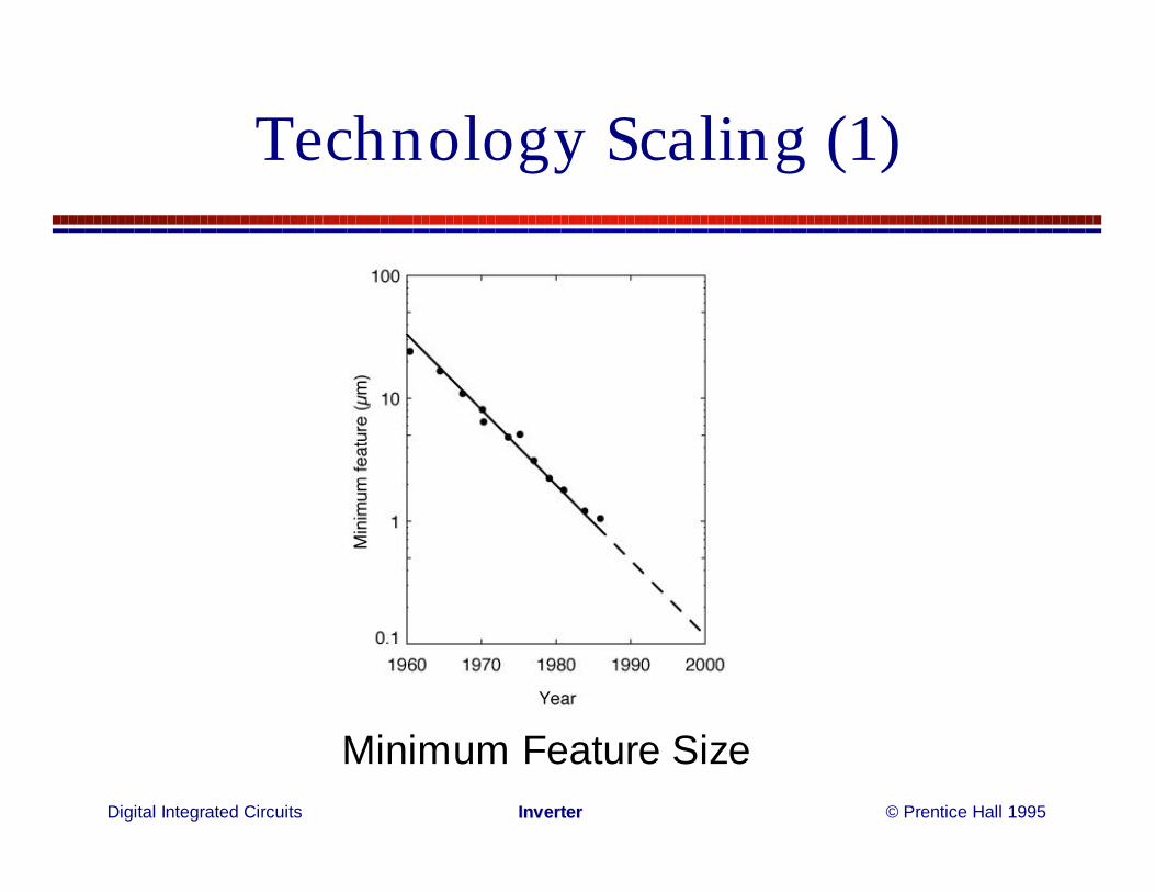
Technology Scaling (1)
Minimum Feature Size

Digital Integrated Circuits © Prentice Hall 1995InverterInverter
Technology Scaling (2)
Number of components per chip

Digital Integrated Circuits © Prentice Hall 1995InverterInverter
Propagation Delay Scaling

Digital Integrated Circuits © Prentice Hall 1995InverterInverter
Technology Scaling Models
• Full Scaling (Constant Electrical Field)
• Fixed Voltage Scaling
• General Scaling
ideal model — dimensions and voltage scaletogether by the same factor S
most common model until recently —only dimensions scale, voltages remain constant
most realistic for todays situation —voltages and dimensions scale with different factors

Digital Integrated Circuits © Prentice Hall 1995InverterInverter
Scaling Relationships for Long ChannelDevices

Digital Integrated Circuits © Prentice Hall 1995InverterInverter
Scaling of Short Channel Devices

Digital Integrated Circuits © Prentice Hall 1995InverterInverter
BIPOLARINVERTERS

Digital Integrated Circuits © Prentice Hall 1995InverterInverter
Resistor-Transistor Logic
Vin
Vout
Vcc
RB
R C
Q1
Vin
Vout
SaturationCutoff
F orward-active
VCE (sat )
V CC
V B E(on) V in(e o s)
VTC of nonsaturating gate

Digital Integrated Circuits © Prentice Hall 1995InverterInverter
VTC of RTL Inverter
0.0 1.0 2.0 3.0 4.0 5.0Vin
0.0
1.0
2.0
3.0
4.0
5.0V
ou
t
FO=5
FO=2
FO=1
FO=0
VOH is function of fan-out

Digital Integrated Circuits © Prentice Hall 1995InverterInverter
Transient Response of RTL Inverter
0.00e+00 5.00e-10 1.00e-09 1.50e-09 2.00e-09t
0.0
1.0
2.0
3.0
4.0
5.0V
out
tp = 290 psec !!!!

Digital Integrated Circuits © Prentice Hall 1995InverterInverter
The ECL Gate at a GlanceVcc
R C
Q1
V c c
R C
Q 2 VrefVin
Vout 2Vou t1
IEE
VEE
Vx
Core of gate:The differential pairor “current switch”

Digital Integrated Circuits © Prentice Hall 1995InverterInverter
Single-ended versusDifferential Logic
VinVin
Vout1 Vout2
Vout 1
Vout 2
Vo ut1Vout2 Vout2Vo ut1
DifferentialSingle-ended

Digital Integrated Circuits © Prentice Hall 1995InverterInverter
Complete ECL GateVcc
R C
Q1
V c c
R C
Q2 Vre fVin
IEE
VEE
Vx
V c cVcc
VEE
R BVout 2Vout 1
Q4Q3VC 1 V C2
Emitter-followeroutput driver
Digital Integrated Circuits © Prentice Hall 1995InverterInverter
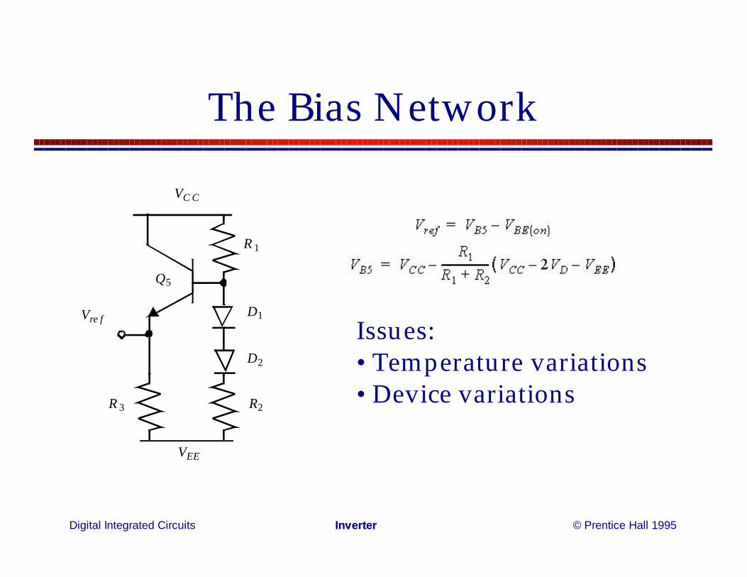
The Bias Network
Q5
R 1
R2R 3
D1
D2
Vre f
VC C
VEE
Issues:•Temperature variations•Device variations

Digital Integrated Circuits © Prentice Hall 1995InverterInverter
Photomicrograph of early ECLGate (1967)

Digital Integrated Circuits © Prentice Hall 1995InverterInverter
ECL VTC
V CC – VBE(on)
VC C – VBE(on) – IEER C
Vin
Vo ut
V out2
Vout1
V ref
+/– n φT
Q 1 s a turates

Digital Integrated Circuits © Prentice Hall 1995InverterInverter
ECL VTC
Vswing = IEE RC

Digital Integrated Circuits © Prentice Hall 1995InverterInverter
Simulated VTC of ECL Gate
–1.5 –1.3 –1.1 –0.9 –0.7 –0.5Vin (V)
–1.30
–1.20
–1.10
–1.00
–0.90
–0.80
–0.70V ou
t (V)
Vout1 Vout2

Digital Integrated Circuits © Prentice Hall 1995InverterInverter
ECL Gate with Single Fan-outV cc
R C
Q1Vin
IE E
VE E
V x
V c c
Q 3
Vcc
RC
Q1
IEE
VEE
R B
V E E
Cd Cbe
Cc s
Cbc Cb c
CbeCd
C beVout1
FAN-O UT
VC 1C bc

Digital Integrated Circuits © Prentice Hall 1995InverterInverter
Simulated Collector Currentsof Differential Pair
0 0.1 0.2Time (nse c )
–1
0
1
Col
lect
or c
urre
nt (n
orm
aliz
ed)
10 mA 5 mA
1 mA
0.5 mA
IC 1
IC 2

Digital Integrated Circuits © Prentice Hall 1995InverterInverter
Propagation Delay of ECL Gate

Digital Integrated Circuits © Prentice Hall 1995InverterInverter
Simulated Transient Responseof ECL Inverter
0 0. 2 0.4 0.6 0. 8 1.0
t (nsec)
–1.30
–1.10
–0.90
–0.70V
(Vo
lt)
V out1V in

Digital Integrated Circuits © Prentice Hall 1995InverterInverter
Propagation Delay as aFunction of Bias Current
0 5 10 15 200
50
100
150
200
IE E (m A)
t pLH
(pse
c)

Digital Integrated Circuits © Prentice Hall 1995InverterInverter
ECL Power Dissipation

Digital Integrated Circuits © Prentice Hall 1995InverterInverter
Scaling Model for Bipolar Inverter

Digital Integrated Circuits © Prentice Hall 1995InverterInverter
Bipolar Scaling
Top Related