Integrated polysilicon and DRIE bulk silicon ...mnsa.ece.wisc.edu/Publications/J1/J1.pdf ·...
10
456 JOURNAL OF MICROELECTROMECHANICAL SYSTEMS, VOL. 8, NO. 4, DECEMBER 1999 Integrated Polysilicon and DRIE Bulk Silicon Micromachining for an Electrostatic Torsional Actuator Jer-Liang Andrew Yeh, Student Member, IEEE, Hongrui Jiang, Student Member, IEEE, and Norman C. Tien, Member, IEEE Abstract— This paper presents a fabrication process that in- tegrates polysilicon surface micromachining and deep reactive ion etching (DRIE) bulk silicon micromachining. The process takes advantage of the design flexibility of polysilicon surface micromachining and the deep silicon structures possible with DRIE. As a demonstration, a torsional actuator driven by a combdrive moving in the out-of-plane direction, consisting of polysilicon fingers and bulk silicon fingers, has been fabricated. The integrated process allows the combdrive to be integrated with any structure made by polysilicon surface micromachining. [433] Index Terms— Asymmetric combdrive, electrostatic torsional actuator, integrated polysilicon and deep reactive ion etching (DRIE) bulk silicon micromachining, levitation, parallel-plate actuator. I. INTRODUCTION S ILICON micromachining has been utilized since the early 1960’s. At its early stage, anisotropic single-crystal silicon etching technology was employed in the majority of the research efforts. In the early 1980’s, surface micromachining using sacrificial etching gave rise to new types of microsensors and microactuators. More recently, deep reactive ion etching (DRIE) technology has given tremendous impetus to high- aspect-ratio dry etching of single-crystal silicon. DRIE bulk silicon micromachining is a fabrication tech- nique that allows one to produce deep structures in a silicon substrate or even movable structures by the use of undercuts. Many fabrication methods have been used to make microstruc- tures out of single-crystal silicon, including single-crystal silicon reactive ion etch and metallization (SCREAM) process [1], deep-etch shallow-diffusion process [2], and silicon-on- insulator (SOI) process. These techniques have several com- mon advantages such as excellent mechanical properties and high-aspect-ratio structures. However, there exist geometric constraints to the types of structures that can be fabricated; some examples are limitations on the maximum width of released beams, difficulty with the integration of membranes parallel to the substrate, and inability to create multiple-level structures with various features (e.g., hinges). The purpose of polysilicon surface micromachining is to fabricate micromechanical structures from deposited thin films. Manuscript received March 22, 1999; revised August 2, 1999. Subject Editor, E. Obermeier. The authors are with Cornell University, Ithaca, NY 14853 USA. Publisher Item Identifier S 1057-7157(99)09611-0. Polysilicon structures anchored to the silicon ground plane are free to move after the underlying sacrificial material is removed. Multiple layers of structural polysilicon and sacrificial layers can be sequentially deposited and patterned in order to realize complex and multilayered structures [3]. Three-dimensional polysilicon structures can be built by fold- ing out the surface structures. Various types of actuators such as the electrostatic interdigitated combdrive [4], the scratch drive actuator [5], and the thermal actuator [6] have been developed to move these microstructures. However, the thinness of the deposited polysilicon film can limit aspects of the device performance such as capacitive sensing signal, electrostatic force, and resonant frequency. In addition, the use of polysilicon brings up some material and fabrication issues that do not appear in bulk micromachining processes such as residual stress, stress gradient through the film, variation of Young’s modulus, topography with multiple-layer structures, and in-use/release stiction. Both DRIE bulk silicon micromachining and polysilicon surface micromachining have merits and demerits when used alone. However, many limitations of one method can be overcome by the other. Integrated polysilicon and DRIE bulk silicon micromachining not only retains the advantages of both methods but also expands the range of structure designs. In addition to the structures that can be made by the individual methods, combinations of surface and bulk methods can be applied to build actuators such as combdrives with fingers asymmetric in height and thickness, parallel-plate actuators, anisotropic springs, and mixtures of beams and membranes [7]. Furthermore, the resonant frequencies of these structures can be designed to be far apart from each other by having them made using either polysilicon surface micromachining or DRIE bulk silicon micromachining. The separation of resonant frequencies benefits structural stability and reduces coupling between structures. II. DEVICE DEMONSTRATION To demonstrate the feasibility of integrated polysilicon and DRIE bulk silicon micromachining, we have fabricated an electrostatic torsional actuator driven by an asymmetric combdrive, shown in Fig. 1, which generates a torque on a polysilicon membrane. Unlike a conventional combdrive where the fingers of both combs are of the same thickness and in the same plane, the distinction of the combdrive we 1057–7157/99$10.00 1999 IEEE
Transcript of Integrated polysilicon and DRIE bulk silicon ...mnsa.ece.wisc.edu/Publications/J1/J1.pdf ·...
456 JOURNAL OF MICROELECTROMECHANICAL SYSTEMS, VOL. 8, NO. 4, DECEMBER 1999
Integrated Polysilicon and DRIE Bulk SiliconMicromachining for an Electrostatic
Torsional ActuatorJer-Liang Andrew Yeh,Student Member, IEEE, Hongrui Jiang,Student Member, IEEE,
and Norman C. Tien,Member, IEEE
Abstract—This paper presents a fabrication process that in-tegrates polysilicon surface micromachining and deep reactiveion etching (DRIE) bulk silicon micromachining. The processtakes advantage of the design flexibility of polysilicon surfacemicromachining and the deep silicon structures possible withDRIE. As a demonstration, a torsional actuator driven by acombdrive moving in the out-of-plane direction, consisting ofpolysilicon fingers and bulk silicon fingers, has been fabricated.The integrated process allows the combdrive to be integrated withany structure made by polysilicon surface micromachining. [433]
Index Terms—Asymmetric combdrive, electrostatic torsionalactuator, integrated polysilicon and deep reactive ion etching(DRIE) bulk silicon micromachining, levitation, parallel-plateactuator.
I. INTRODUCTION
SILICON micromachining has been utilized since the early1960’s. At its early stage, anisotropic single-crystal silicon
etching technology was employed in the majority of theresearch efforts. In the early 1980’s, surface micromachiningusing sacrificial etching gave rise to new types of microsensorsand microactuators. More recently, deep reactive ion etching(DRIE) technology has given tremendous impetus to high-aspect-ratio dry etching of single-crystal silicon.
DRIE bulk silicon micromachining is a fabrication tech-nique that allows one to produce deep structures in a siliconsubstrate or even movable structures by the use of undercuts.Many fabrication methods have been used to make microstruc-tures out of single-crystal silicon, including single-crystalsilicon reactive ion etch and metallization (SCREAM) process[1], deep-etch shallow-diffusion process [2], and silicon-on-insulator (SOI) process. These techniques have several com-mon advantages such as excellent mechanical properties andhigh-aspect-ratio structures. However, there exist geometricconstraints to the types of structures that can be fabricated;some examples are limitations on the maximum width ofreleased beams, difficulty with the integration of membranesparallel to the substrate, and inability to create multiple-levelstructures with various features (e.g., hinges).
The purpose of polysilicon surface micromachining is tofabricate micromechanical structures from deposited thin films.
Manuscript received March 22, 1999; revised August 2, 1999. SubjectEditor, E. Obermeier.
The authors are with Cornell University, Ithaca, NY 14853 USA.Publisher Item Identifier S 1057-7157(99)09611-0.
Polysilicon structures anchored to the silicon ground planeare free to move after the underlying sacrificial materialis removed. Multiple layers of structural polysilicon andsacrificial layers can be sequentially deposited and patternedin order to realize complex and multilayered structures [3].Three-dimensional polysilicon structures can be built by fold-ing out the surface structures. Various types of actuatorssuch as the electrostatic interdigitated combdrive [4], thescratch drive actuator [5], and the thermal actuator [6] havebeen developed to move these microstructures. However, thethinness of the deposited polysilicon film can limit aspectsof the device performance such as capacitive sensing signal,electrostatic force, and resonant frequency. In addition, the useof polysilicon brings up some material and fabrication issuesthat do not appear in bulk micromachining processes such asresidual stress, stress gradient through the film, variation ofYoung’s modulus, topography with multiple-layer structures,and in-use/release stiction.
Both DRIE bulk silicon micromachining and polysiliconsurface micromachining have merits and demerits when usedalone. However, many limitations of one method can beovercome by the other. Integrated polysilicon and DRIE bulksilicon micromachining not only retains the advantages of bothmethods but also expands the range of structure designs. Inaddition to the structures that can be made by the individualmethods, combinations of surface and bulk methods can beapplied to build actuators such as combdrives with fingersasymmetric in height and thickness, parallel-plate actuators,anisotropic springs, and mixtures of beams and membranes[7]. Furthermore, the resonant frequencies of these structurescan be designed to be far apart from each other by havingthem made using either polysilicon surface micromachining orDRIE bulk silicon micromachining. The separation of resonantfrequencies benefits structural stability and reduces couplingbetween structures.
II. DEVICE DEMONSTRATION
To demonstrate the feasibility of integrated polysiliconand DRIE bulk silicon micromachining, we have fabricatedan electrostatic torsional actuator driven by an asymmetriccombdrive, shown in Fig. 1, which generates a torque ona polysilicon membrane. Unlike a conventional combdrivewhere the fingers of both combs are of the same thicknessand in the same plane, the distinction of the combdrive we
1057–7157/99$10.00 1999 IEEE

YEH et al.: INTEGRATED POLYSILICON AND DRIE BULK SILICON MICROMACHINING 457
Fig. 1. Closeup SEM of a fabricated asymmetric combdrive formed by (upper) polysilicon fingers and (lower) bulk silicon fingers.
Fig. 2. Schematic of a device actuated by asymmetric combdrives.
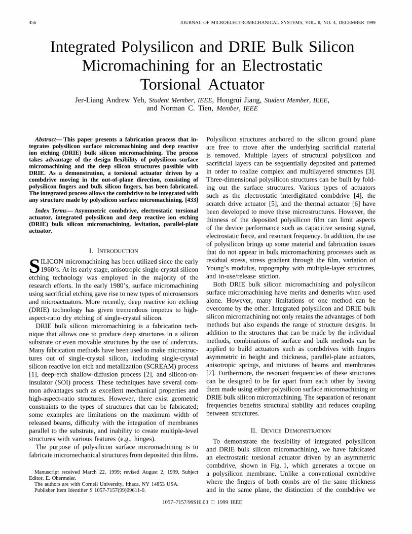
present is that the fingers on one comb are thinner and higherthan those on the other comb. Actuation is achieved whenthe thin polysilicon fingers are pulled downward toward thesubstrate with respect to the fixed thick bulk silicon fingersunder a voltage applied between the combs (see Fig. 2). Thepulldown of the movable comb is the result of fringing electricfield, shown in Fig. 3, on the polysilicon fingers, which createstorsional motion. The asymmetry in height and thickness ofcomb fingers causes a net fringing capacitance that points
down into the substrate. Note that the actuator’s differentialcapacitance varies with the position of the movable polysiliconfingers. Hence, this combdrive cannot generate a constantoutput torque due to its position-dependent differential capac-itance.
Present approaches for producing torsional motion by elec-trostatic actuators include parallel-plate actuators [8]–[13],in-plane interdigitated combdrives utilizing the out-of-planefringing force [14], [15], and in-plane interdigitated comb-
458 JOURNAL OF MICROELECTROMECHANICAL SYSTEMS, VOL. 8, NO. 4, DECEMBER 1999
Fig. 3. Schematic of the electric field lines in an asymmetric combdrive.
drives used to swing structures such as a plate connected toit by a hinge. An example is the folded-up scanning mirrorsdriven by combdrives [16], [17]. In those structures, dynamicproblems such as coupling, backlash, and low resonant fre-quency can be encountered. Coupling between torsional andtranslational motions results in the instability of the device.Backlash occurs at the moment when the direction of motionis changing because of the clearance between the pin and thestaple. In devices where torsional motion can be generatedby in-plane interdigitated combdrives, the maximum angle ofrotation is limited.
Typically, large rotational motion is achieved using aparallel-plate actuator. Asymmetric combdrives fabricated byintegrated polysilicon and DRIE bulk silicon micromachiningare an alternative that offers better dynamic performance for alarge rotational motion. The static and dynamic performanceof a parallel-plate actuator and our combdrive are discussed inSection IV. Given constraints on rotation angle and resonantfrequency, it is found that a membrane will twist at a loweroperating voltage with this asymmetric combdrive than witha parallel-plate actuator [18].
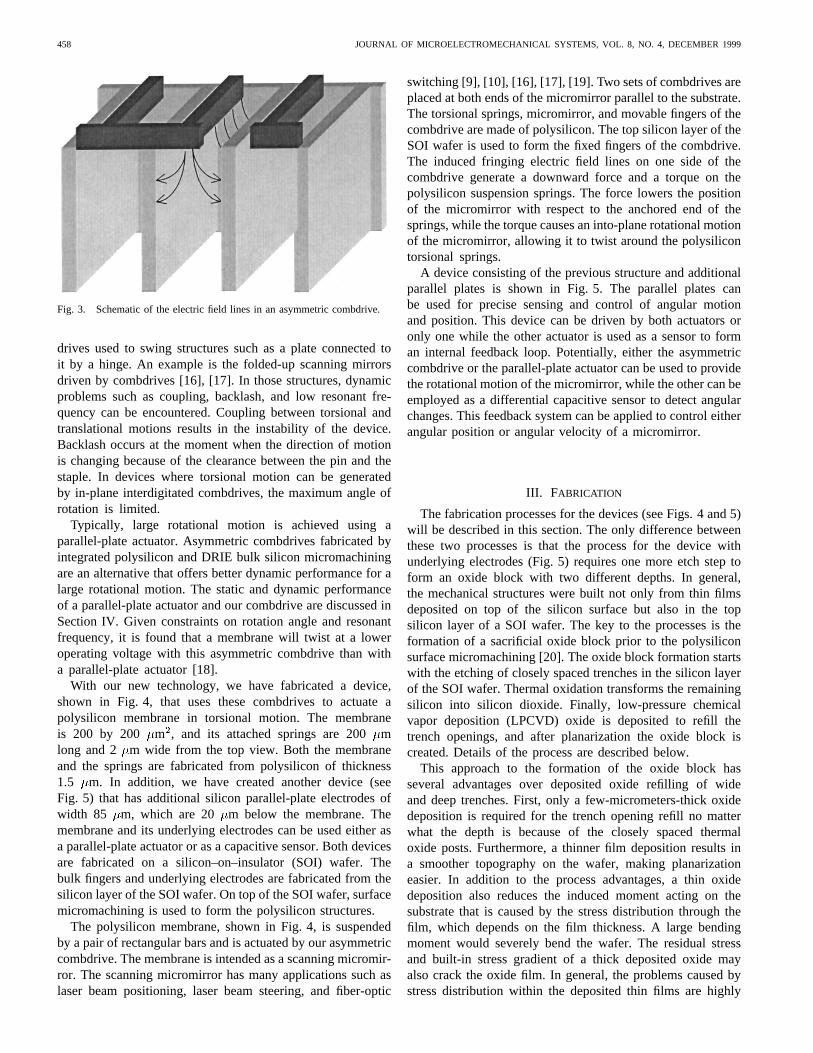
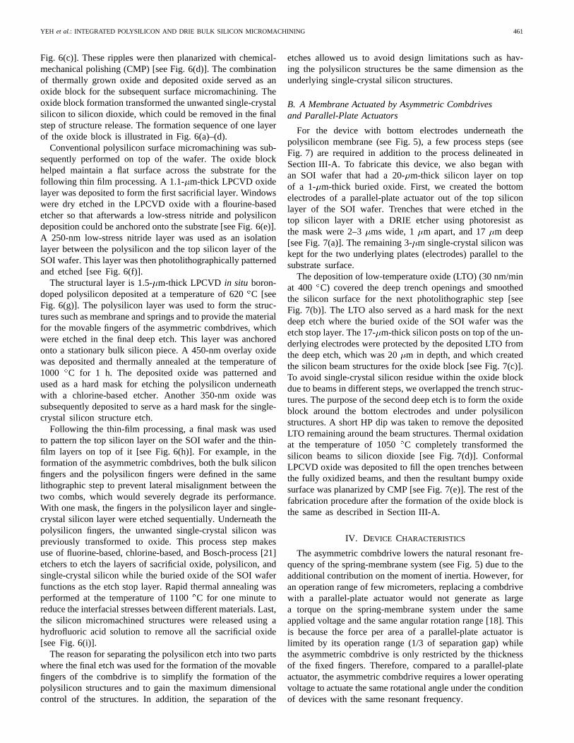
With our new technology, we have fabricated a device,shown in Fig. 4, that uses these combdrives to actuate apolysilicon membrane in torsional motion. The membraneis 200 by 200 m , and its attached springs are 200mlong and 2 m wide from the top view. Both the membraneand the springs are fabricated from polysilicon of thickness1.5 m. In addition, we have created another device (seeFig. 5) that has additional silicon parallel-plate electrodes ofwidth 85 m, which are 20 m below the membrane. Themembrane and its underlying electrodes can be used either asa parallel-plate actuator or as a capacitive sensor. Both devicesare fabricated on a silicon–on–insulator (SOI) wafer. Thebulk fingers and underlying electrodes are fabricated from thesilicon layer of the SOI wafer. On top of the SOI wafer, surfacemicromachining is used to form the polysilicon structures.
The polysilicon membrane, shown in Fig. 4, is suspendedby a pair of rectangular bars and is actuated by our asymmetriccombdrive. The membrane is intended as a scanning micromir-ror. The scanning micromirror has many applications such aslaser beam positioning, laser beam steering, and fiber-optic
switching [9], [10], [16], [17], [19]. Two sets of combdrives areplaced at both ends of the micromirror parallel to the substrate.The torsional springs, micromirror, and movable fingers of thecombdrive are made of polysilicon. The top silicon layer of theSOI wafer is used to form the fixed fingers of the combdrive.The induced fringing electric field lines on one side of thecombdrive generate a downward force and a torque on thepolysilicon suspension springs. The force lowers the positionof the micromirror with respect to the anchored end of thesprings, while the torque causes an into-plane rotational motionof the micromirror, allowing it to twist around the polysilicontorsional springs.
A device consisting of the previous structure and additionalparallel plates is shown in Fig. 5. The parallel plates canbe used for precise sensing and control of angular motionand position. This device can be driven by both actuators oronly one while the other actuator is used as a sensor to forman internal feedback loop. Potentially, either the asymmetriccombdrive or the parallel-plate actuator can be used to providethe rotational motion of the micromirror, while the other can beemployed as a differential capacitive sensor to detect angularchanges. This feedback system can be applied to control eitherangular position or angular velocity of a micromirror.
III. FABRICATION
The fabrication processes for the devices (see Figs. 4 and 5)will be described in this section. The only difference betweenthese two processes is that the process for the device withunderlying electrodes (Fig. 5) requires one more etch step toform an oxide block with two different depths. In general,the mechanical structures were built not only from thin filmsdeposited on top of the silicon surface but also in the topsilicon layer of a SOI wafer. The key to the processes is theformation of a sacrificial oxide block prior to the polysiliconsurface micromachining [20]. The oxide block formation startswith the etching of closely spaced trenches in the silicon layerof the SOI wafer. Thermal oxidation transforms the remainingsilicon into silicon dioxide. Finally, low-pressure chemicalvapor deposition (LPCVD) oxide is deposited to refill thetrench openings, and after planarization the oxide block iscreated. Details of the process are described below.
This approach to the formation of the oxide block hasseveral advantages over deposited oxide refilling of wideand deep trenches. First, only a few-micrometers-thick oxidedeposition is required for the trench opening refill no matterwhat the depth is because of the closely spaced thermaloxide posts. Furthermore, a thinner film deposition results ina smoother topography on the wafer, making planarizationeasier. In addition to the process advantages, a thin oxidedeposition also reduces the induced moment acting on thesubstrate that is caused by the stress distribution through thefilm, which depends on the film thickness. A large bendingmoment would severely bend the wafer. The residual stressand built-in stress gradient of a thick deposited oxide mayalso crack the oxide film. In general, the problems caused bystress distribution within the deposited thin films are highly
YEH et al.: INTEGRATED POLYSILICON AND DRIE BULK SILICON MICROMACHINING 459
Fig. 4. SEM of a fabricated asymmetric-combdrive actuated membrane.
Fig. 5. SEM of a fabricated dually actuated membrane. The etch holes are used to speed up the wet etch release of the structures.
dependent on the film thickness and greatly reduced with ourtechnique.
A. A Membrane Actuated by Asymmetric Combdrives
The process sequence used to fabricate the membrane andasymmetric combdrives (see Fig. 4) is depicted schematically
460 JOURNAL OF MICROELECTROMECHANICAL SYSTEMS, VOL. 8, NO. 4, DECEMBER 1999
(a) (f)
(b) (g)
(c) (h)
(d) (i)
(e)
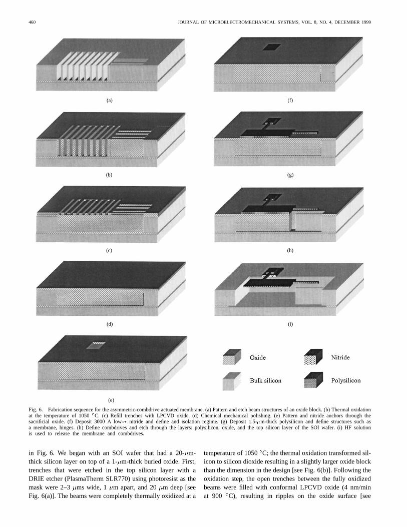
Fig. 6. Fabrication sequence for the asymmetric-combdrive actuated membrane. (a) Pattern and etch beam structures of an oxide block. (b) Thermal oxidationat the temperature of 1050�C. (c) Refill trenches with LPCVD oxide. (d) Chemical mechanical polishing. (e) Pattern and nitride anchors through thesacrificial oxide. (f) Deposit 3000 A low-� nitride and define and isolation regime. (g) Deposit 1.5-�m-thick polysilicon and define structures such asa membrane, hinges. (h) Define combdrives and etch through the layers: polysilicon, oxide, and the top silicon layer of the SOI wafer. (i) HF solutionis used to release the membrane and combdrives.
in Fig. 6. We began with an SOI wafer that had a 20-m-thick silicon layer on top of a 1-m-thick buried oxide. First,trenches that were etched in the top silicon layer with aDRIE etcher (PlasmaTherm SLR770) using photoresist as themask were 2–3 ms wide, 1 m apart, and 20 m deep [seeFig. 6(a)]. The beams were completely thermally oxidized at a
temperature of 1050C; the thermal oxidation transformed sil-icon to silicon dioxide resulting in a slightly larger oxide blockthan the dimension in the design [see Fig. 6(b)]. Following theoxidation step, the open trenches between the fully oxidizedbeams were filled with conformal LPCVD oxide (4 nm/minat 900 C), resulting in ripples on the oxide surface [see
YEH et al.: INTEGRATED POLYSILICON AND DRIE BULK SILICON MICROMACHINING 461
Fig. 6(c)]. These ripples were then planarized with chemical-mechanical polishing (CMP) [see Fig. 6(d)]. The combinationof thermally grown oxide and deposited oxide served as anoxide block for the subsequent surface micromachining. Theoxide block formation transformed the unwanted single-crystalsilicon to silicon dioxide, which could be removed in the finalstep of structure release. The formation sequence of one layerof the oxide block is illustrated in Fig. 6(a)–(d).
Conventional polysilicon surface micromachining was sub-sequently performed on top of the wafer. The oxide blockhelped maintain a flat surface across the substrate for thefollowing thin film processing. A 1.1-m-thick LPCVD oxidelayer was deposited to form the first sacrificial layer. Windowswere dry etched in the LPCVD oxide with a flourine-basedetcher so that afterwards a low-stress nitride and polysilicondeposition could be anchored onto the substrate [see Fig. 6(e)].A 250-nm low-stress nitride layer was used as an isolationlayer between the polysilicon and the top silicon layer of theSOI wafer. This layer was then photolithographically patternedand etched [see Fig. 6(f)].
The structural layer is 1.5-m-thick LPCVD in situ boron-doped polysilicon deposited at a temperature of 620C [seeFig. 6(g)]. The polysilicon layer was used to form the struc-tures such as membrane and springs and to provide the materialfor the movable fingers of the asymmetric combdrives, whichwere etched in the final deep etch. This layer was anchoredonto a stationary bulk silicon piece. A 450-nm overlay oxidewas deposited and thermally annealed at the temperature of1000 C for 1 h. The deposited oxide was patterned andused as a hard mask for etching the polysilicon underneathwith a chlorine-based etcher. Another 350-nm oxide wassubsequently deposited to serve as a hard mask for the single-crystal silicon structure etch.
Following the thin-film processing, a final mask was usedto pattern the top silicon layer on the SOI wafer and the thin-film layers on top of it [see Fig. 6(h)]. For example, in theformation of the asymmetric combdrives, both the bulk siliconfingers and the polysilicon fingers were defined in the samelithographic step to prevent lateral misalignment between thetwo combs, which would severely degrade its performance.With one mask, the fingers in the polysilicon layer and single-crystal silicon layer were etched sequentially. Underneath thepolysilicon fingers, the unwanted single-crystal silicon waspreviously transformed to oxide. This process step makesuse of fluorine-based, chlorine-based, and Bosch-process [21]etchers to etch the layers of sacrificial oxide, polysilicon, andsingle-crystal silicon while the buried oxide of the SOI waferfunctions as the etch stop layer. Rapid thermal annealing wasperformed at the temperature of 1100C for one minute toreduce the interfacial stresses between different materials. Last,the silicon micromachined structures were released using ahydrofluoric acid solution to remove all the sacrificial oxide[see Fig. 6(i)].
The reason for separating the polysilicon etch into two partswhere the final etch was used for the formation of the movablefingers of the combdrive is to simplify the formation of thepolysilicon structures and to gain the maximum dimensionalcontrol of the structures. In addition, the separation of the
etches allowed us to avoid design limitations such as hav-ing the polysilicon structures be the same dimension as theunderlying single-crystal silicon structures.
B. A Membrane Actuated by Asymmetric Combdrivesand Parallel-Plate Actuators
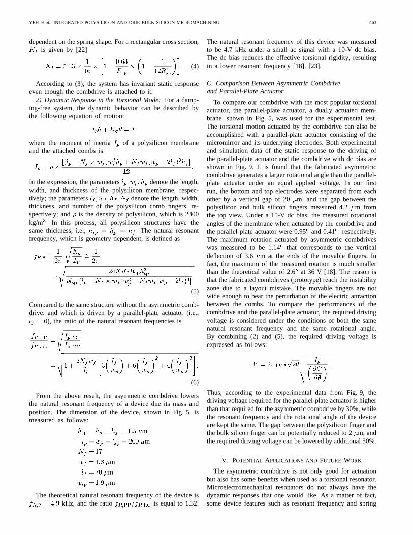
For the device with bottom electrodes underneath thepolysilicon membrane (see Fig. 5), a few process steps (seeFig. 7) are required in addition to the process delineated inSection III-A. To fabricate this device, we also began withan SOI wafer that had a 20-m-thick silicon layer on topof a 1- m-thick buried oxide. First, we created the bottomelectrodes of a parallel-plate actuator out of the top siliconlayer of the SOI wafer. Trenches that were etched in thetop silicon layer with a DRIE etcher using photoresist asthe mask were 2–3 ms wide, 1 m apart, and 17 m deep[see Fig. 7(a)]. The remaining 3-m single-crystal silicon waskept for the two underlying plates (electrodes) parallel to thesubstrate surface.
The deposition of low-temperature oxide (LTO) (30 nm/minat 400 C) covered the deep trench openings and smoothedthe silicon surface for the next photolithographic step [seeFig. 7(b)]. The LTO also served as a hard mask for the nextdeep etch where the buried oxide of the SOI wafer was theetch stop layer. The 17-m-thick silicon posts on top of the un-derlying electrodes were protected by the deposited LTO fromthe deep etch, which was 20m in depth, and which createdthe silicon beam structures for the oxide block [see Fig. 7(c)].To avoid single-crystal silicon residue within the oxide blockdue to beams in different steps, we overlapped the trench struc-tures. The purpose of the second deep etch is to form the oxideblock around the bottom electrodes and under polysiliconstructures. A short HP dip was taken to remove the depositedLTO remaining around the beam structures. Thermal oxidationat the temperature of 1050C completely transformed thesilicon beams to silicon dioxide [see Fig. 7(d)]. ConformalLPCVD oxide was deposited to fill the open trenches betweenthe fully oxidized beams, and then the resultant bumpy oxidesurface was planarized by CMP [see Fig. 7(e)]. The rest of thefabrication procedure after the formation of the oxide block isthe same as described in Section III-A.
IV. DEVICE CHARACTERISTICS
The asymmetric combdrive lowers the natural resonant fre-quency of the spring-membrane system (see Fig. 5) due to theadditional contribution on the moment of inertia. However, foran operation range of few micrometers, replacing a combdrivewith a parallel-plate actuator would not generate as largea torque on the spring-membrane system under the sameapplied voltage and the same angular rotation range [18]. Thisis because the force per area of a parallel-plate actuator islimited by its operation range (1/3 of separation gap) whilethe asymmetric combdrive is only restricted by the thicknessof the fixed fingers. Therefore, compared to a parallel-plateactuator, the asymmetric combdrive requires a lower operatingvoltage to actuate the same rotational angle under the conditionof devices with the same resonant frequency.
462 JOURNAL OF MICROELECTROMECHANICAL SYSTEMS, VOL. 8, NO. 4, DECEMBER 1999
(a)
(b)
(c)
(d)
(e)
Fig. 7. Fabrication sequence of the electrodes underneath a membrane. (a)Pattern and etch beam structures 17�m deep using DRIE. (b) Fill trencheswith LPCVD oxide. (c) Pattern and etch beam structures through the topsilicon layer using DRIE. (d) Thermal oxidation at a temperature of 1050�C.(e) Refill trenches with LPCVD oxide and then do chemical mechanicalpolishing.
A. Asymmetric Combdrive Forces and Torques
The asymmetric combdrive formed by a set of polysiliconmovable fingers and bulk silicon fixed fingers is actuated bythe fringing capacitance that is due to the different thicknessesand heights of the two combs. The majority of the inducedfringing electric field lines in this combdrive point downwardtoward the substrate rather than in an in-plane direction,which is just the opposite of what occurs in the conventionalin-plane interdigitated combdrive. This type of electrostaticcombdrive does not have invariant force output with respectto displacement as in an in-plane interdigitated combdrive,though their geometric shapes from the top view look similar.
The output force and torque due to the changing capacitance,which are expressed in (1) and (2), vary with the position ofthe polysilicon comb fingers.
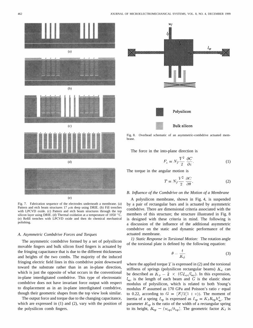
Fig. 8. Overhead schematic of an asymmetric-combdrive actuated mem-brane.
The force in the into-plane direction is
(1)
The torque in the angular motion is
(2)
B. Influence of the Combdrive on the Motion of a Membrane
A polysilicon membrane, shown in Fig. 4, is suspendedby a pair of rectangular bars and is actuated by asymmetriccombdrive. There are dimensional criteria associated with themembers of this structure; the structure illustrated in Fig. 8is designed with these criteria in mind. The following isa discussion of the influence of the additional asymmetriccombdrive on the static and dynamic performance of theactuated membrane.
1) Static Response in Torsional Motion:The rotation angleof the torsional plate is defined by the following equation:
(3)
where the applied torque is expressed in (2) and the torsionalstiffness of springs (polysilicon rectangular beams) canbe described as In this expression,
is the length of each beam and is the elastic shearmodulus of polysilicon, which is related to both Young’smodulus assumed as 170 GPa and Poisson’s ratioequalto 0.22, according to The moment ofinertia of a spring is expressed as Theparameter is the ratio of the width of a rectangular springto its height, The geometric factor is
YEH et al.: INTEGRATED POLYSILICON AND DRIE BULK SILICON MICROMACHINING 463
dependent on the spring shape. For a rectangular cross section,is given by [22]
(4)
According to (3), the system has invariant static responseeven though the combdrive is attached to it.
2) Dynamic Response in the Torsional Mode:For a damp-ing-free system, the dynamic behavior can be described bythe following equation of motion:
where the moment of inertia of a polysilicon membraneand the attached combs is
In the expression, the parameters denote the length,width, and thickness of the polysilicon membrane, respec-tively; the parameters denote the length, width,thickness, and number of the polysilicon comb fingers, re-spectively; and is the density of polysilicon, which is 2300kg/m In this process, all polysilicon structures have thesame thickness, i.e., The natural resonantfrequency, which is geometry dependent, is defined as
(5)
Compared to the same structure without the asymmetric comb-drive, and which is driven by a parallel-plate actuator (i.e.,
), the ratio of the natural resonant frequencies is
(6)
From the above result, the asymmetric combdrive lowersthe natural resonant frequency of a device due its mass andposition. The dimension of the device, shown in Fig. 5, ismeasured as follows:
m
m
m
m
m
The theoretical natural resonant frequency of the device iskHz, and the ratio is equal to 1.32.
The natural resonant frequency of this device was measuredto be 4.7 kHz under a small ac signal with a 10-V dc bias.The dc bias reduces the effective torsional rigidity, resultingin a lower resonant frequency [18], [23].
C. Comparison Between Asymmetric Combdriveand Parallel-Plate Actuator
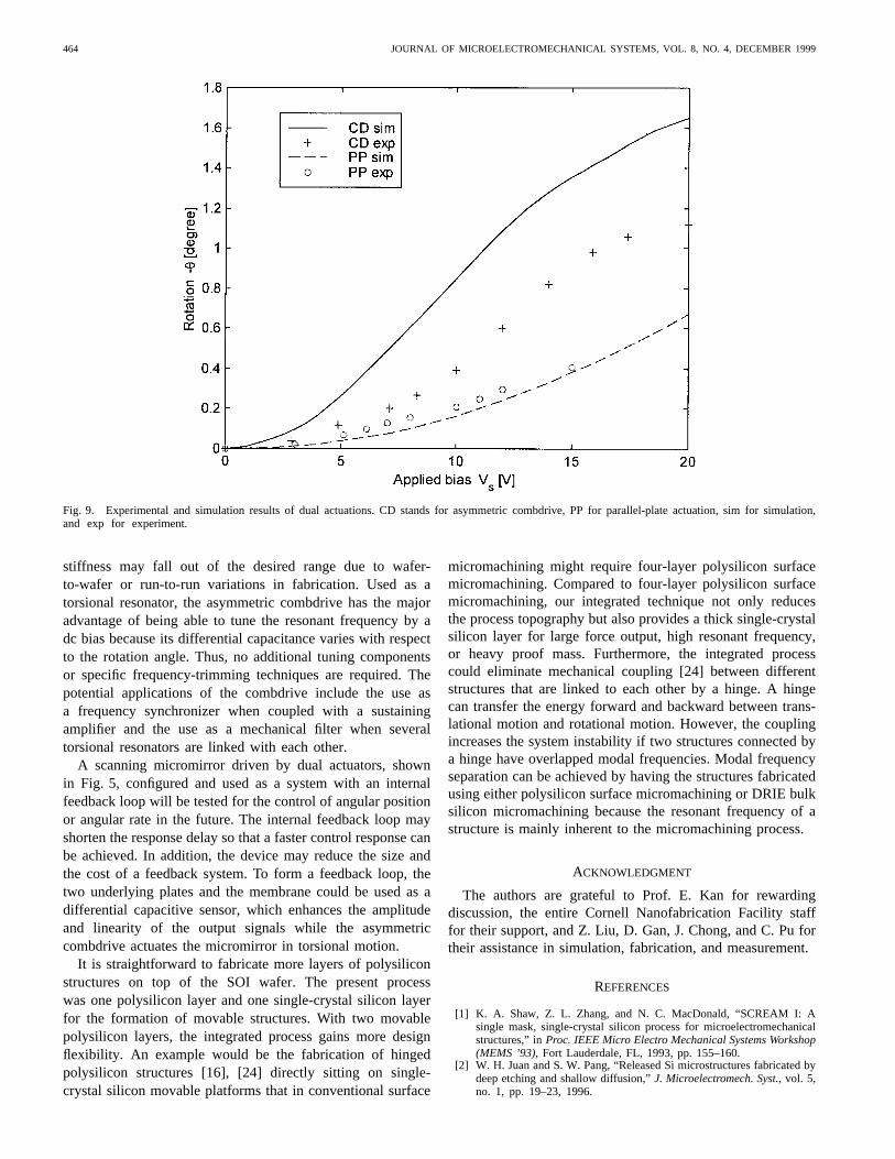
To compare our combdrive with the most popular torsionalactuator, the parallel-plate actuator, a dually actuated mem-brane, shown in Fig. 5, was used for the experimental test.The torsional motion actuated by the combdrive can also beaccomplished with a parallel-plate actuator consisting of themicromirror and its underlying electrodes. Both experimentaland simulation data of the static response to the driving ofthe parallel-plate actuator and the combdrive with dc bias areshown in Fig. 9. It is found that the fabricated asymmetriccombdrive generates a larger rotational angle than the parallel-plate actuator under an equal applied voltage. In our firstrun, the bottom and top electrodes were separated from eachother by a vertical gap of 20 m, and the gap between thepolysilicon and bulk silicon fingers measured 4.2m fromthe top view. Under a 15-V dc bias, the measured rotationalangles of the membrane when actuated by the combdrive andthe parallel-plate actuator were 0.95and 0.41 respectively.The maximum rotation actuated by asymmetric combdriveswas measured to be 1.14that corresponds to the verticaldeflection of 3.6 m at the ends of the movable fingers. Infact, the maximum of the measured rotation is much smallerthan the theoretical value of 2.6at 36 V [18]. The reason isthat the fabricated combdrives (prototype) reach the instabilityzone due to a layout mistake. The movable fingers are notwide enough to bear the perturbation of the electric attractionbetween the combs. To compare the performances of thecombdrive and the parallel-plate actuator, the required drivingvoltage is considered under the conditions of both the samenatural resonant frequency and the same rotational angle.By combining (2) and (5), the required driving voltage isexpressed as follows:
Thus, according to the experimental data from Fig. 9, thedriving voltage required for the parallel-plate actuator is higherthan that required for the asymmetric combdrive by 30%, whilethe resonant frequency and the rotational angle of the deviceare kept the same. The gap between the polysilicon finger andthe bulk silicon finger can be potentially reduced to 2m, andthe required driving voltage can be lowered by additional 50%.
V. POTENTIAL APPLICATIONS AND FUTURE WORK
The asymmetric combdrive is not only good for actuationbut also has some benefits when used as a torsional resonator.Microelectromechanical resonators do not always have thedynamic responses that one would like. As a matter of fact,some device features such as resonant frequency and spring
464 JOURNAL OF MICROELECTROMECHANICAL SYSTEMS, VOL. 8, NO. 4, DECEMBER 1999
Fig. 9. Experimental and simulation results of dual actuations. CD stands for asymmetric combdrive, PP for parallel-plate actuation, sim for simulation,and exp for experiment.
stiffness may fall out of the desired range due to wafer-to-wafer or run-to-run variations in fabrication. Used as atorsional resonator, the asymmetric combdrive has the majoradvantage of being able to tune the resonant frequency by adc bias because its differential capacitance varies with respectto the rotation angle. Thus, no additional tuning componentsor specific frequency-trimming techniques are required. Thepotential applications of the combdrive include the use asa frequency synchronizer when coupled with a sustainingamplifier and the use as a mechanical filter when severaltorsional resonators are linked with each other.
A scanning micromirror driven by dual actuators, shownin Fig. 5, configured and used as a system with an internalfeedback loop will be tested for the control of angular positionor angular rate in the future. The internal feedback loop mayshorten the response delay so that a faster control response canbe achieved. In addition, the device may reduce the size andthe cost of a feedback system. To form a feedback loop, thetwo underlying plates and the membrane could be used as adifferential capacitive sensor, which enhances the amplitudeand linearity of the output signals while the asymmetriccombdrive actuates the micromirror in torsional motion.
It is straightforward to fabricate more layers of polysiliconstructures on top of the SOI wafer. The present processwas one polysilicon layer and one single-crystal silicon layerfor the formation of movable structures. With two movablepolysilicon layers, the integrated process gains more designflexibility. An example would be the fabrication of hingedpolysilicon structures [16], [24] directly sitting on single-crystal silicon movable platforms that in conventional surface
micromachining might require four-layer polysilicon surfacemicromachining. Compared to four-layer polysilicon surfacemicromachining, our integrated technique not only reducesthe process topography but also provides a thick single-crystalsilicon layer for large force output, high resonant frequency,or heavy proof mass. Furthermore, the integrated processcould eliminate mechanical coupling [24] between differentstructures that are linked to each other by a hinge. A hingecan transfer the energy forward and backward between trans-lational motion and rotational motion. However, the couplingincreases the system instability if two structures connected bya hinge have overlapped modal frequencies. Modal frequencyseparation can be achieved by having the structures fabricatedusing either polysilicon surface micromachining or DRIE bulksilicon micromachining because the resonant frequency of astructure is mainly inherent to the micromachining process.
ACKNOWLEDGMENT
The authors are grateful to Prof. E. Kan for rewardingdiscussion, the entire Cornell Nanofabrication Facility stafffor their support, and Z. Liu, D. Gan, J. Chong, and C. Pu fortheir assistance in simulation, fabrication, and measurement.
REFERENCES
[1] K. A. Shaw, Z. L. Zhang, and N. C. MacDonald, “SCREAM I: Asingle mask, single-crystal silicon process for microelectromechanicalstructures,” inProc. IEEE Micro Electro Mechanical Systems Workshop(MEMS ’93), Fort Lauderdale, FL, 1993, pp. 155–160.
[2] W. H. Juan and S. W. Pang, “Released Si microstructures fabricated bydeep etching and shallow diffusion,”J. Microelectromech. Syst., vol. 5,no. 1, pp. 19–23, 1996.
YEH et al.: INTEGRATED POLYSILICON AND DRIE BULK SILICON MICROMACHINING 465
[3] M. Rodgers and J. Sniegowski, “5-level polysilicon surface microma-chine technology: Application to complex mechanical systems,” inProc.IEEE Solid State Sensors and Actuators Workshops (Hilton Head’98),June 1998, pp. 144–149.
[4] W. C. Tang, T.-C. H. Nguyen, M. W. Judy, and R. T. Howe, “Electro-static combdrive of lateral polysilicon resonators,”Sens. Actuators, vol.A21-23, pp. 328–331, 1990.
[5] T. Akiyama and K. Shono, “Controlled stepwise motion in polysiliconmicrostructures,”J. Microelectromech. Syst., vol. 2, no. 3, pp. 106–110,1993.
[6] H. Guckel, J. Klein, T. Christenson, K. Skrobis, M. Laudon, and E.Lovell, “Thermo-magnetic metal flexure actuators,” inProc. IEEE SolidState Sensors and Actuators Workshops (Hilton Head’92), June 1992,pp. 73–75.
[7] M. Lutz, W. Golderer, J. Gerstenmeier, J. Marek, B. Maihofer, S.Mahler, H. Munzel, and U. Bischof, “A precision yaw rate sensor insilicon micromachining,” inProc. 9th Int. Conf. Sensors and Actuators(Transducer ’97), Chicago, IL, June 1997, pp. 847–850.
[8] K. E. Peterson, “Silicon torsional scanning mirror,”IBM J. Res. De-velop., vol. 24, no. 5, 1980, pp. 631–637.
[9] L. Hornbeck, “Current status of the digital micromirror device (DMD)for projection television applications,” inProc. IEEE Int. ElectronDevices Meeting, Washington, DC, Dec. 1993, pp. 381–384.
[10] D. L. Dickensheet and G. S. Kino, “Silicon-micromachined scanningconfocal optical microscope,”J. Microelectromech. Syst., vol. 7, no. 1,pp. 38–47, 1998.
[11] T. Gessner, W. Dotzel, D. Billep, R. Hahn, C. Kaufmann, S. Kurth, K.Kehr, C. Steiniger, and U. Wollmann, “Silicon mirror arrays fabricatedby using bulk- and surface-micromachining,” inProc. SPIE, San Jose,CA, Feb. 1997, vol. 3008, pp. 256–305.
[12] W. Dotzel, T. Gessner, R. Hahn, C. Kaufmann, K. Kehr, S. Kurth, and J.Mehner, “Silicon mirrors and micromirror arrays for spatial laser beammodulation,” inProc. 9th Int. Conf. Sensors and Actuators (Transducer’97), Chicago, IL, June 1997, pp. 81–84.
[13] J. Kraenert, C. Deter, T. Gessner, and W. Dotzel, “Laser displaytechnology,” inProc. IEEE Micro Electro Mechanical Systems Workshop(MEMS ’93), Heidelberg, Germany, 1998, p. 99.
[14] S. A. Miller, K. L. Turner, and N. C. MacDonald, “Microelectrome-chanical scanning probe instruments for array architectures,”Rev. Sci.Instrum., vol. 68, Nov. 1997, pp. 4155–4162.
[15] W. C. Tang, M. G. Lim, and R. T. Howe, “Electrostatic comb drivelevitation and control method,”J. Microelectromech. Syst., vol. 1, no.4, pp. 170–178, 1992.
[16] M.-H. Kiang, O. Solgaard, K. Y. Lay, and R. S. Muller, “Electrostaticcombdrive-actuated micromirror for laser-beam scanning and position-ing,” J. Microelectromech. Syst., vol. 7, no. 1, pp. 27–37, 1998.
[17] N. C. Tien, M.-H. Kiang, M. J. Daneman, O. Solgaard, K. Y. Lau, andR. S. Muller, “Actuation of polysilicon surface-micromachined mirror,”in Proc. SPIE 1996 Int. Symp. Lasers and Optoelectronics, San Jose,CA, vol. 2687, 1996, pp. 53–59.
[18] J.-L. A. Yeh, N. C. Tien, and C.-Y. Hui, submitted for publication.[19] H. Toshiyoshi and H. Fujita, “Electrostatic micro torsion mirrors for an
optical switch matrix,”J. Microelectromech. Syst., vol. 5, no. 4, p. 231,1996.
[20] H. B. Erzgraber, T. Grabolla, H. H. Richter, P. Schley, and A. Wolff,“A novel buried oxide isolation for monolithic RF inductors on silicon,”in Proc. Int. Electron Devices Meeting (IEDM ’98), Dec. 1998, pp.535–539.
[21] F. Laermer and A. Schilp, “Method of anisotropically etching silicon,”U.S. Patent 5 501 893, Aug. 5, 1994.
[22] G. M. Gere and S. P. Timoshenko,Mechanics of Materials, 3rd ed.Boston, MA: PWS-KENT, 1990
[23] K. B. Lee and Y.-H. Cho, “A triangular electrostatic comb array formicromechanical resonant frequency tuning,”Sens. Actuators, vol. 70,pp. 112–117, 1998.
[24] R. S. Muller and K. Y. Lau, “Surface-micromachined microopticalelements and systems,”Proc. IEEE, vol. 86, pp. 1705–1720, Aug. 1998.
Jer-Liang Andrew Yeh (S’97) received the B.S.degree in mechanical engineering from the NationalTaiwan University, Taiwan, R.O.C., in 1992 andthe M. Eng. degree in mechanical engineering andin electrical engineering from Cornell University,Ithaca, NY, in 1996 and 1997, respectively, wherehe is currently pursing the Ph.D. degree in electricalengineering.
His research interests include design and fabrica-tion of MEMS systems, micromechanics issues inmicromachined structures, and MEMS elements for
bio-mimicked devices.
Hongrui Jiang (S’98) was born in Xi’an, China, in1973. He received the B.S. degree in physics fromPeking University, China, in 1995. He is currentlypursuing the Ph.D. degree in electrical engineeringat Cornell University, Ithaca, NY.
His research interest is mainly in applications ofMEMS in RF circuits.
Norman C. Tien (S’87–M’89) received the B.S. degree from the University ofCalifornia, Berkeley, the M.S. degree from the University of Illinois, Urbana-Champaign, and the Ph.D. degree from the University of California, San Diegoin 1993.
He is an Assistant Professor in the School of Electrical Engineeringat Cornell University, Ithaca, NY, where his research interest is in thedevelopment of silicon microelectromechanical systems (MEMS), includingthe design and fabrication of microactuators, microsensors, micromechanicalstructures, and systems. From 1993 to 1996, he was a Lecturer in theDepartment of Electrical Engineering and Computer Science at the Universityof California, Berkeley, and a Postdoctoral Research Engineer associated withthe Berkeley Sensor & Actuator Center. Between 1984 and 1986, he was aSilicon Process Development Engineer with Polaroid Corp., Cambridge, MA.