Lecture 4 Fabrication pathways to micro/nano scale systems ...
date post
19-Dec-2015Category
view
216download
0
Welcome to the Australian National Fabrication Facility
Matthew Chen [email protected]
Providing nano and micro-fabrication facilities for Australia’s researchers

Outline
What is ANFF?
What can ANFF do for you?
Around the Nodes
Accessing ANFF

= + Tools?

What is ANFF?
A central organisation that provides access to a network of facilities and instrumentation across 8 university based nodes
Associated technical expertise to assist with your fabrication needs
National network allows access to a broad range of capabilities and expertise from across Australia
VIC/MCN
Materials
OptoFab
NSW
QLD
ACT
WA
OptoFab
NSWSouth Aust
QLD
ACT
WA
VIC/MCN
Materials

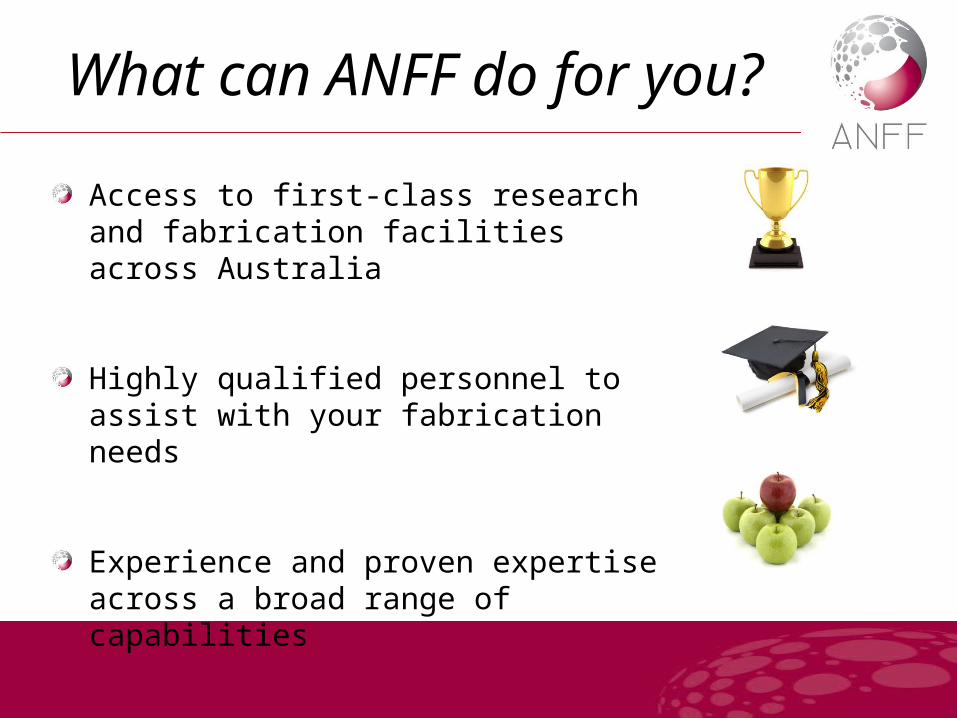
What can ANFF do for you?
Access to first-class research and fabrication facilities across Australia
Highly qualified personnel to assist with your fabrication needs
Experience and proven expertise across a broad range of capabilities

Nanoelectronics & photonics
Ultra-high resolution EBL
Semiconductor processing
Advanced deposition and etching
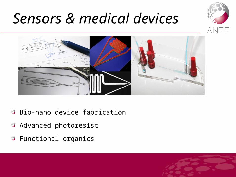
Bio-nano device fabrication
Advanced photoresist
Functional organics
Sensors & medical devices
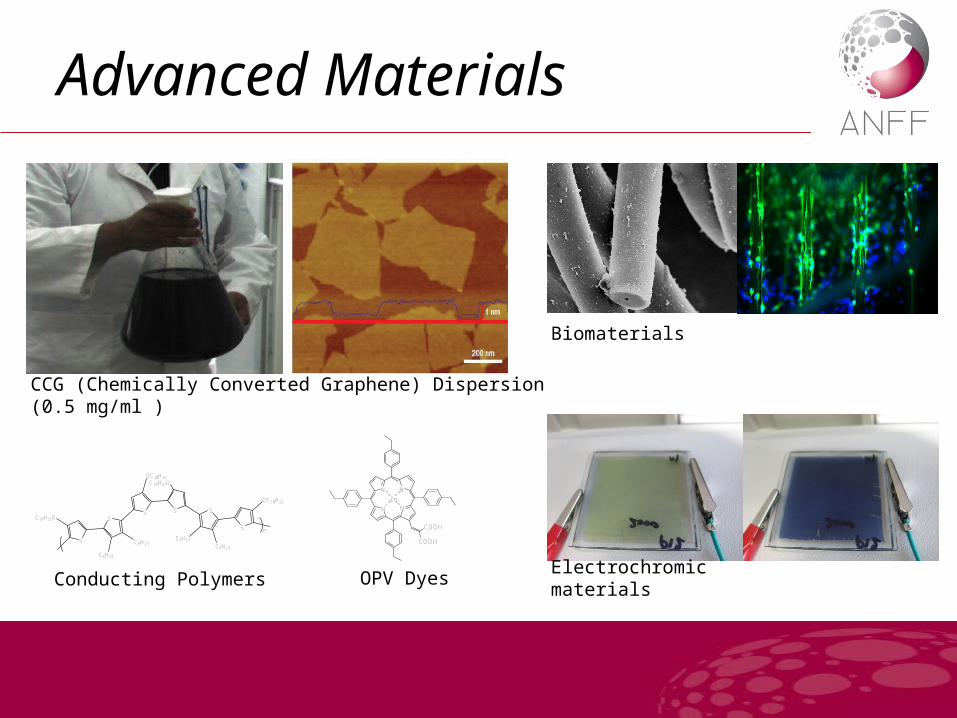
Advanced Materials
CCG (Chemically Converted Graphene) Dispersion (0.5 mg/ml )
Conducting Polymers
SS
S
S
S
SC10H21O
OC10H21C10H21O
OC10H21
C6H13
C6H13
C6H13
C6H13
n
NN
N N
COOH
Zn
COOH
OPV Dyes
Biomaterials
Electrochromic materials

Process scaling
Fibre Spinning
Reel-to-reel printing
Ability to process large wafers
Pilot scale synthesis
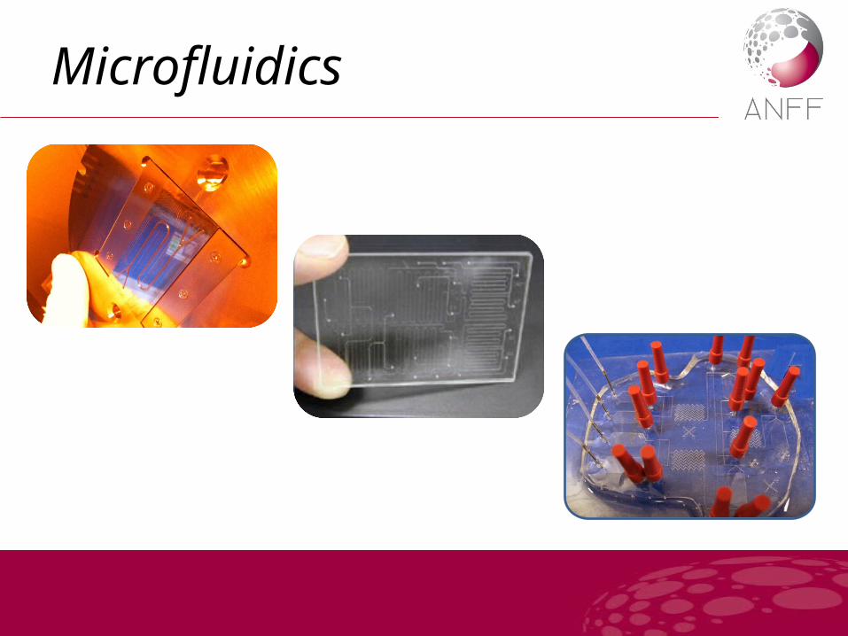
Microfluidics

Linking expertise
VIC/MCN
Materials
OptoFab
NSW
QLD
ACT
WA
OptoFab
NSWSouth Aust
QLD
ACT
WA
VIC/MCN
Materials

NSW Node
Single electron reader, representing a significant breakthrough in Si-based quantum computation [see Morello et al, Nature 467, 687 (2010)].
Silicon quantum dot, produced by CQCT using ANFF-NSW’s facilities
Featured on the cover of Applied Physics Letters [Lim et al, Applied Physics Letters 94, 173502 (2009)].
User highlights
Key expertise: Nanoelectronics and nano-spintronics
Key capabilities: - High resolution electron beam lithography- Si MOS process line- Advanced deposition and etching

ACT NodeKey expertise: – III-V Compound Semiconductors
– Optoelectronics, waveguides, photonic crystals, Micro electromechanical systems (MEMS)
Key capabilities: – Growth of III-V compound semiconductor multilayers– Electron beam lithography– Advanced deposition and etching
Photonic chips made by CUDOS using ANFF ACT’s facilities.
The chips were made from chalcogenide glass, allowing nonlinear optics in optimized materials and nanostructures, enabling high speed information processing beyond limits of electronics,
User highlights

WA NodeKey expertise: – II-VI Compound semiconductors
– Optical nano/micro electromechanical systems – Infra-red array /sensor technology
Key capabilities: – Integrated II-VI semiconductor growth, device fabrication, processing to device packaging & characterization
– Advanced deposition and etching
‘Coloured' Infrared - researchers at the ANFF WA node created a minaturised hyperspectral spectrometer on a chip that enables colour vision in infra-red night vision
User highlights
Cavity Length, dV
Mirror
Mirror
IncidentIR
ReflectedIR
Detector
Silicon Nitride
0.0%
25.0%
50.0%
75.0%
100.0%
2000 2200 2400 2600 2800 3000 3200Wavelength (nm)
Tran
smis
sion
d = 1700nmd = 900nm

OptoFab NodeKey expertise: – Optical materials, components and devices
– Laser micro-machining
Key capabilities: – Advanced photolithography (e.g. photomask production)– Optical characterisation – Optical fibre and Lithium niobate device fabrication– Laser micro-machining
Olympic torches for the Sydney 2000 and Athens 2004 Olympics
Nozzle outlet were laser machined by the frequency doubled Nd:YAG laser
User highlights
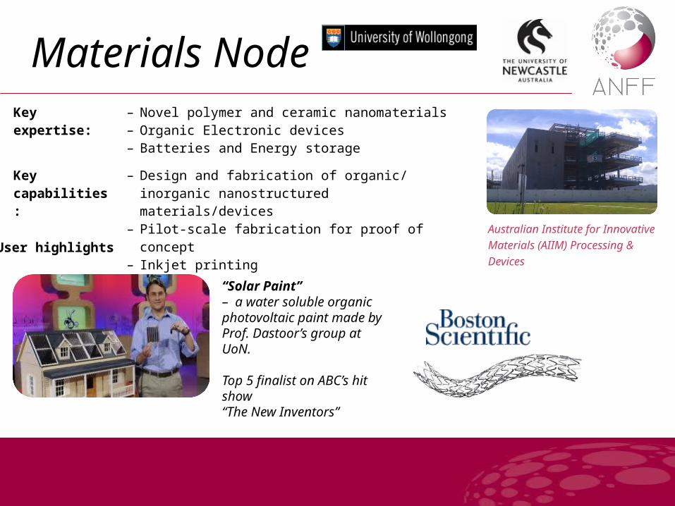
Materials NodeKey expertise: – Novel polymer and ceramic nanomaterials
– Organic Electronic devices– Batteries and Energy storage
Key capabilities: – Design and fabrication of organic/ inorganic nanostructured materials/devices
– Pilot-scale fabrication for proof of concept– Inkjet printing
“Solar Paint” – a water soluble organic photovoltaic paint made by Prof. Dastoor’s group at UoN.
Top 5 finalist on ABC’s hit show “The New Inventors”
User highlightsAustralian Institute for Innovative Materials (AIIM) Processing & Devices

Queensland NodeKey expertise: Bio-Micro-Nano Devices Design, Fabrication and Characterisation
Key capabilities: – Advanced photoresist synthesis– Bio-nano device fabrication– Functional organic/polymer and bio-inspired nanomaterials– Surface and device characterisation– Fabrication and Processing of Silica Carbide (SiC)
User highlights
Non Invasive Saliva diagnostic device : For early detection of cardiovascular diseases. Immunoassay of biomarkers performed in 15min rather than 2 hrs.

South Australian NodeKey expertise: – Microfluidic devices
– Micro and nano scale patterning
Key capabilities: – Prototyping and replication of micro-scale channels– Chemical and physical surface functionalisation and
characterisation– Texturing and patterning of surfaces
Solvent Extraction Microchip - a schematic of a chip created by the Ian Wark institute.
Has the ability to process 100x faster than large scale solvent extraction.
Priest, C., et al., Microfluidic extraction of copper from particle-laden solutions, Int. J. Miner. Process. (2010),http://dx.doi.org/10.1016/j.minpro.2010.11.005
User highlights

Victorian NodeKey expertise: Unique facility comprising of both biological and non-
biological nano-fabrication techniques
Key capabilities: – Photo- and electron beam lithography– Advanced deposition and etching– Rapid prototyping– Novel techniques such as embossing, inkjet printing and
electroforming.
Flagship instruments
EBL (Vistec EBPG5000PLUS)
<10nm resolution
Fastest system in Australia.
High res dual-beam Helios FIB/ SEM
One of only 3 in Australia.
Photolithography System (EVG620 UV)
Can take up to 150mm substrates.
DRIEs
2xPlasmalab 100 ICP380
Laser scanning Confocal microscope (Nikon A1Rsi MP)
Biologoical AFM
Deposition Equipments
- PECVD- Ion assisted DC/RF
Sputtering- E-Beam and
Thermal Evaporator

Melbourne Centre of Nanofabrication (MCN)
₋ Photolithography₋ E-beam₋ SEM
₋ Polymer Electronics
₋ PVD & RIE₋ Electroplating₋ Characterisation
Lab₋ Wet Chemistry
₋ PC2 Lab₋ Microscopy ₋ Bio-chem lab₋ Nanoparticle lab₋ PDMS lab
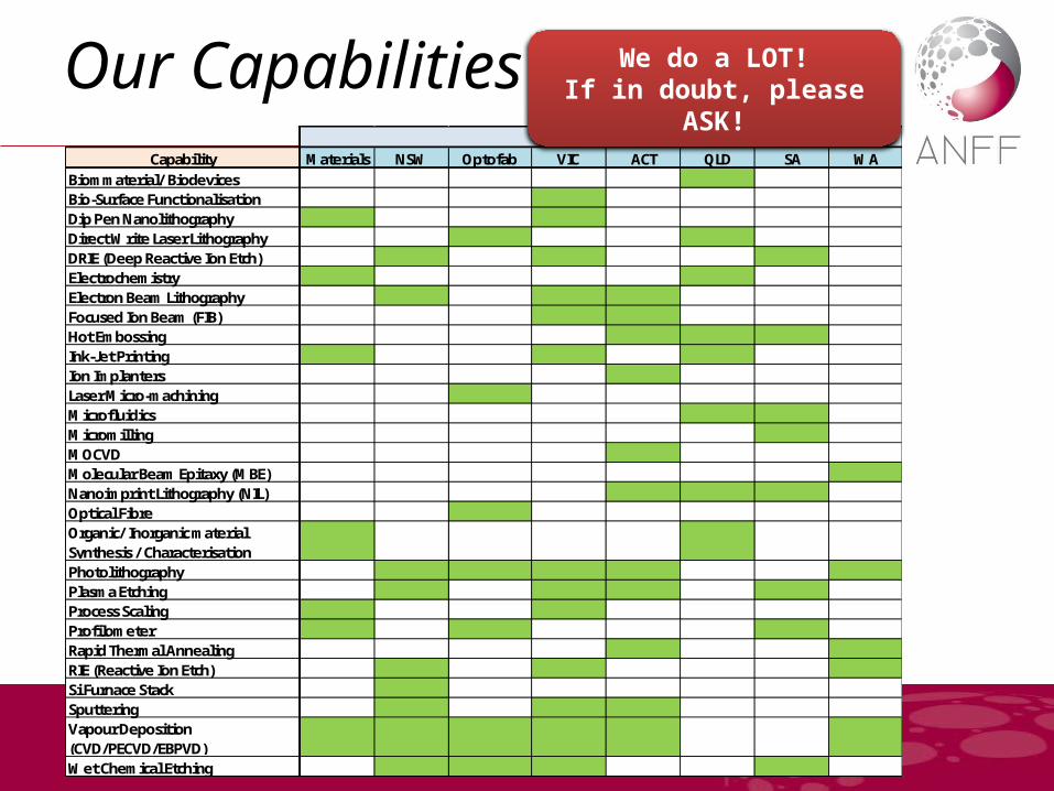
Our CapabilitiesCapability Materials NSW Optofab VIC ACT QLD SA WA
Biommaterial/ BiodevicesBio-Surface FunctionalisationDip Pen NanolithographyDirect Write Laser LithographyDRIE (Deep Reactive Ion Etch)ElectrochemistryElectron Beam LithographyFocused Ion Beam (FIB)Hot EmbossingInk-Jet PrintingIon ImplantersLaser Micro-machiningMicrofluidicsMicromillingMOCVDMolecular Beam Epitaxy (MBE)Nanoimprint Lithography (NIL)Optical Fibre Organic/ Inorganic materialSynthesis / CharacterisationPhotolithographyPlasma EtchingProcess ScalingProfilometerRapid Thermal AnnealingRIE (Reactive Ion Etch)Si Furnace StackSputteringVapour Deposition(CVD/PECVD/EBPVD)Wet Chemical Etching
Node
We do a LOT!If in doubt, please ASK!

Accessing ANFF
ANFF Users– University researchers– Government funded research centres– Industry, SMEs, start-ups
Accessing Costs– Access to instruments and relevant training are
charged at hourly rates – Rates vary according to the instrument requested– Speciality materials or devices may be fabricated by
Process Engineers for an additional cost
ANYONE interested in nanofabrication

Access Procedure
Contact ANFF
Contact Node
Approval Process
Complete User Proposal
Access Committee
User InductionTraining
Job performed by ANFF staff
New user?
YES NO
Assess requestfeasibility
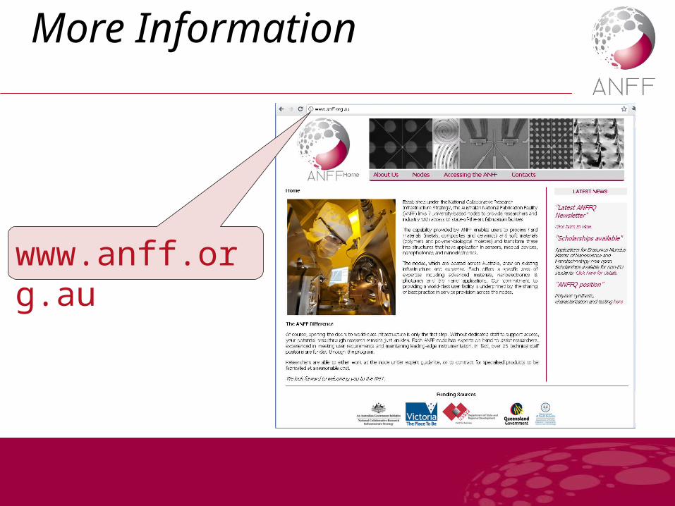
More Information
www.anff.org.au

Acknowledgements

BANFF

Providing nano and micro-fabrication facilities for Australia’s researchers
www.anff.org.au