Nano Fabrication Research at FIU - Homepage - CMU · 2005-02-18 · Center for Nano Materials &...
13
Center for Nano Materials & Devices Nano Fabrication Research at FIU Professor W. Choi’s Nano Materials and Devices Lab Nanotechnology processing Facilities in FIU (AMRIE) FIU logo with 25nm line width by e-beam lithography • Fastest growing University in the US- Ranked in top 25 largest Universities (34,000 students) • Research I status- highest ranking in shortest time • Minority Institution- designated a Hispanic Serving Inst itution (HIS) - only one of two with Research I status • External research in excess 0f $60MM, with 20% growt h every year for the past 6 years • College of Engineering (COE) offers Ph.D. in ME, EE, CE and MS in MSE, BioMed, Environ. Eng., IE, Eng. M anagement. Ph.D. in Materials Science in process
Transcript of Nano Fabrication Research at FIU - Homepage - CMU · 2005-02-18 · Center for Nano Materials &...

Center for Nano Materials & Devices
Nano Fabrication Research at FIUProfessor W. Choi’s Nano Materials and Devices Lab
Nanotechnology processing Facilities in FIU (AMRIE)
FIU logo with 25nm line width by e-beam lithography
• Fastest growing University in the US- Ranked in top 25 largest Universities (34,000 students)• Research I status- highest ranking in shortest time• Minority Institution- designated a Hispanic Serving Institution (HIS) - only one of two with Research I status • External research in excess 0f $60MM, with 20% growth every year for the past 6 years• College of Engineering (COE) offers Ph.D. in ME, EE, CE and MS in MSE, BioMed, Environ. Eng., IE, Eng. Management. Ph.D. in Materials Science in process
Center for Nano Materials & Devices
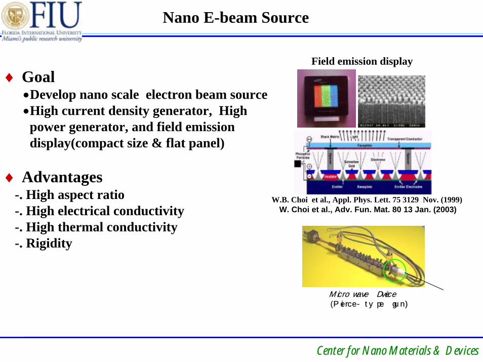
Nano E-beam Source
♦ Goal•Develop nano scale electron beam source•High current density generator, High power generator, and field emission display(compact size & flat panel)
♦ Advantages-. High aspect ratio-. High electrical conductivity-. High thermal conductivity-. Rigidity
Field emission display
W.B. Choi et al., Appl. Phys. Lett. 75 3129 Nov. (1999)W. Choi et al., Adv. Fun. Mat. 80 13 Jan. (2003)
Microwave Device(Pierce-type gun)
gun

Center for Nano Materials & Devices
Selective Growth and Vertically aligned Carbon nanotubes
- Number of graphitic wall is controlled by size of catalyst particle.- Field emission properties is being investigated with structural change.
4 walls 10 walls 25 walls(Y. Choi et al. Appl. Phys. Lett.)
Center for Nano Materials & Devices
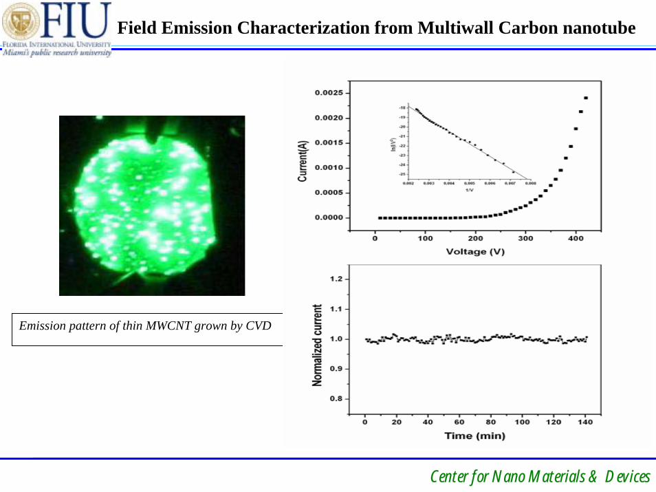
Field Emission Characterization from Multiwall Carbon nanotube
Emission pattern of thin MWCNT grown by CVD

Center for Nano Materials & Devices
CNT for Electronics
• Low dimension --> Tera-level high density device
• Low power consumption
• High current carrying capacity (1 X 10 10 A/cm2)
• Heat dissipation (6000 W/m.K)
• High mobility (Quasi Ballistic) for charge transport
gate
Insulator
Source electrode
Drainelectrode
Nanotube

Center for Nano Materials & Devices
Y-shape CNT arrays
-0.4 -0.2 0.0 0.2 0.4-160
-120
-80
-40
0
40
80
120
160
curr
ent(µ
A)
bias voltage(V)
straight CNT y-junction CNT
SEM image of straight CNT
I-V data of straight- & Y-shape CNTSEM image of Y-shape CNT
W. Choi et al, Nanotechnology 2004
Center for Nano Materials & Devices
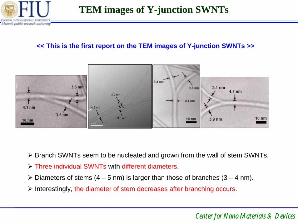
TEM images of Y-junction SWNTs
<< This is the first report on the TEM images of Y-junction SWNTs >>
4.9 nm
4.0 nm
3.8 nm
Branch SWNTs seem to be nucleated and grown from the wall of stem SWNTs.
Three individual SWNTs with different diameters.
Diameters of stems (4 – 5 nm) is larger than those of branches (3 – 4 nm).
Interestingly, the diameter of stem decreases after branching occurs.
Center for Nano Materials & Devices
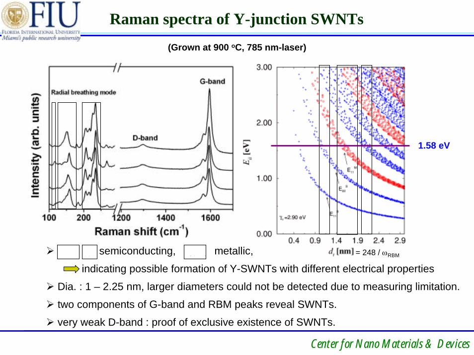
Raman spectra of Y-junction SWNTs
(Grown at 900 oC, 785 nm-laser)
semiconducting, metallic,
indicating possible formation of Y-SWNTs with different electrical properties
Dia. : 1 – 2.25 nm, larger diameters could not be detected due to measuring limitation.
two components of G-band and RBM peaks reveal SWNTs.
very weak D-band : proof of exclusive existence of SWNTs.
= 248 / ωRBM
1.58 eV

Center for Nano Materials & Devices
Raman spectra of Y-junction SWNTs(Grown at 900 oC, 514.5 nm-laser)
2.4 eV
This also show the existence of both metallic and semiconducting SWNTs.

Center for Nano Materials & Devices
CNTs for Sensor
OH OH OH OH
Substrate
Analyte
Mediator-CNT
CNT
1 µm
CNT
Atomic Force Microscope of CNT-Sensor
WB Choi et al. , Appl. Phys. Lett. Nov. 19 79 (2001)
Center for Nano Materials & Devices
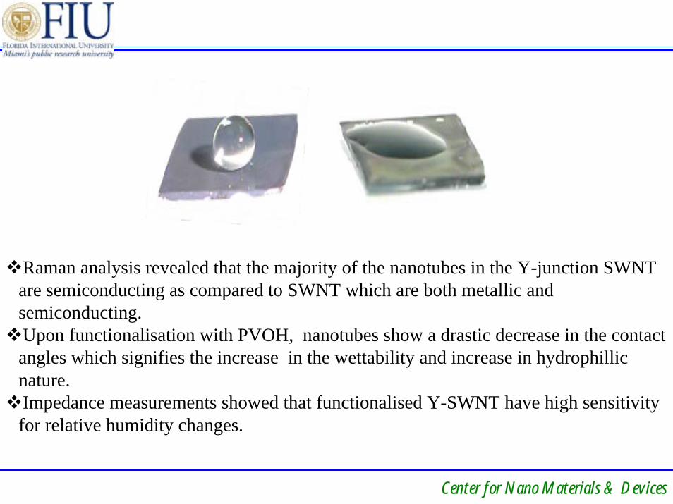
Raman analysis revealed that the majority of the nanotubes in the Y-junction SWNT are semiconducting as compared to SWNT which are both metallic and semiconducting.Upon functionalisation with PVOH, nanotubes show a drastic decrease in the contact angles which signifies the increase in the wettability and increase in hydrophillic nature. Impedance measurements showed that functionalised Y-SWNT have high sensitivity for relative humidity changes.
Center for Nano Materials & Devices
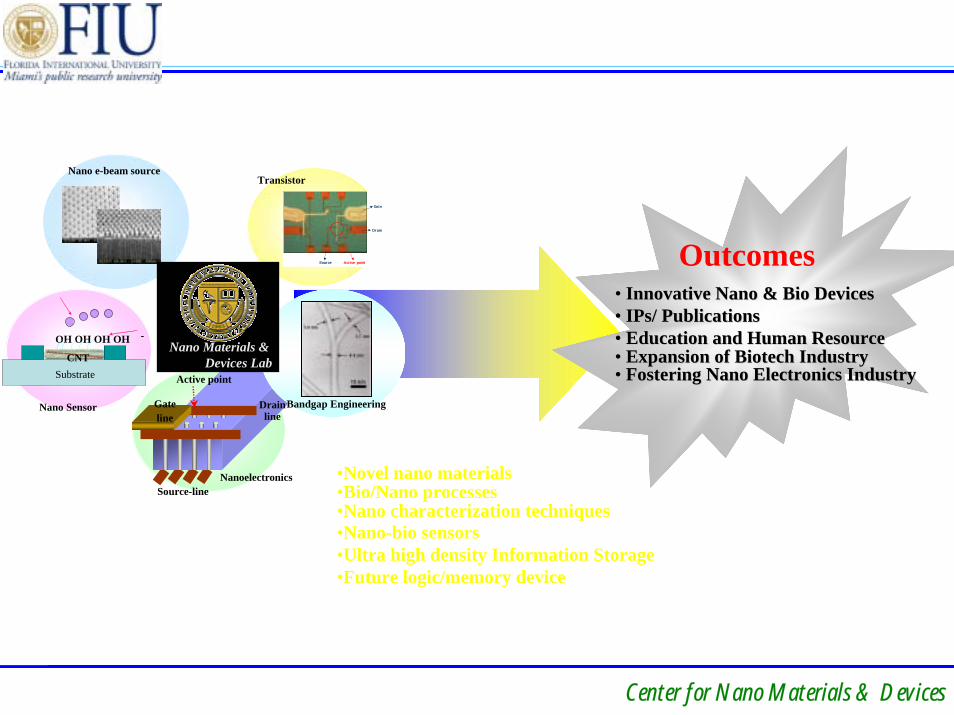
•Novel nano materials•Bio/Nano processes •Nano characterization techniques•Nano-bio sensors•Ultra high density Information Storage•Future logic/memory device
•• Innovative Innovative NanoNano & Bio Devices& Bio Devices•• IPsIPs/ Publications/ Publications•• Education and Human ResourceEducation and Human Resource•• Expansion of Biotech Industry Expansion of Biotech Industry •• Fostering Fostering NanoNano Electronics IndustryElectronics Industry
Outcomes
Source-line
Gate line
Drainline
Active point
Nanoelectronics
Nano e-beam source
Bandgap EngineeringNano Sensor
Transistor
Carbon nanotubeSource
Drain
Gate
Active point
OH OH OH OH
Substrate
-
CNTNano Materials &
Devices Lab

Center for Nano Materials & Devices
Director: Prof. Wonbong ChoiResearch Scientist:
Dr. Somaneth RoyDr. Do-hyun KimDr. Young-chul Choi (Samsung)
Ph.D. Students: Jun HuangHarindra Vedala_NarasimhaRaghunandan SeelaboyinaYong GaoRao BangaloreMichael Mellow