
VLV RI $GYDQFHG 0DWHULDOV 8VLQJ ,RQ %HDP...
145
Advances in Materials Science and Engineering Guest Editors: Adam Georg Balogh, Koumei Baba, David D. Cohen, Robert G. Elliman, Wolfgang Ensinger, and Joseph Gyulai
Transcript of VLV RI $GYDQFHG 0DWHULDOV 8VLQJ ,RQ %HDP...

Advances in Materials Science and Engineering
Guest Editors: Adam Georg Balogh, Koumei Baba, David D. Cohen, Robert G. Elliman, Wolfgang Ensinger, and Joseph Gyulai

Modification, Synthesis, and Analysis ofAdvanced Materials Using Ion Beam Techniques
Advances in Materials Science and Engineering
Modification, Synthesis, and Analysis ofAdvanced Materials Using Ion Beam Techniques
Guest Editors: Adam Georg Balogh, Koumei Baba,David D. Cohen, Robert G. Elliman, Wolfgang Ensinger,and Joseph Gyulai

Copyright © 2012 Hindawi Publishing Corporation. All rights reserved.
This is a special issue published in “Advances in Materials Science and Engineering.” All articles are open access articles distributed underthe Creative Commons Attribution License, which permits unrestricted use, distribution, and reproduction in any medium, providedthe original work is properly cited.

Editorial Board
Marcel Ausloos, BelgiumRobert S. Averback, USAV. Awana, IndiaAmit Bandyopadhyay, USAZ. Barber, UKMark Blamire, UKSusmita Bose, USASteve Bull, UKDavid Cann, USADaolun Chen, CanadaManish U. Chhowalla, USAPaolo Colombo, ItalyMartin Crimp, USAJie Dai, SingaporeC. K. Das, IndiaChris Davies, AustraliaJ. Paulo Davim, PortugalSeshu Babu Desu, USAYong Ding, USAShi Xue Dou, AustraliaChunying Duan, ChinaNadia El-Masry, USADavid Field, USAQiang Fu, ChinaJohn W. Gillespie, USAJeffrey T. Glass, USAZhennan Gu, ChinaHiroki Habazaki, JapanRichard Hennig, USA
Dachamir Hotza, BrazilChun-Hway Hsueh, USARui Huang, USAShyh-Chin Huang, TaiwanJacques Huot, CanadaHamlin Jennings, USAWilliam A. Jesser, USAAdo Jorio, BrazilKazuro Kageyama, JapanS. Komarneni, USAPrashant Kumta, USAPearl Lee-Sullivan, CanadaPavel Lejcek, Czech RepublicMarkku Leskela, FinlandJun Li, SingaporeJing Li, USAYuanhua Lin, ChinaZhimin Liu, ChinaMeilin Liu, GeorgiaMaria A. Loi, The NetherlandsHai Lu, ChinaYiu-Wing Mai, AustraliaPeter Majewski, AustraliaAbdel Makhlouf, GermanyR. S. Mishra, USAS. Miyazaki, JapanPaul Munroe, AustraliaKorukonda L. Murty, USALuigi Nicolais, Italy
Tsutomu Ohzuku, JapanXiaoqing Pan, USAG. Ramanath, USARaju V. Ramanujan, SingaporeJainagesh A. Sekhar, USAYou Song, ChinaCharles Sorrell, AustraliaSteven L. Suib, USAWen-Hua Sun, ChinaSam-Shajing Sun, USAAchim Trampert, GermanyAn-Pang Tsai, JapanVladimir Tsukruk, USAKrystyn Van Vliet, USAStan Veprek, GermanyRui Vilar, PortugalLianzhou Wang, AustraliaKunpeng Wang, ChinaJohn Wang, SingaporeJorg Wiezorek, USAAiguo Xu, ChinaJenn-Ming Yang, USAYadong Yin, USAJihong Yu, ChinaGuan-Jun Zhang, ChinaDao Hua Zhang, SingaporeMing-Xing Zhang, Australia

Contents
Modification, Synthesis, and Analysis of Advanced Materials Using Ion Beam Techniques,Adam Georg Balogh, Koumei Baba, David D. Cohen, Robert G. Elliman, Wolfgang Ensinger,and Joseph GyulaiVolume 2012, Article ID 431297, 2 pages
Mechanical and Structural Properties of Fluorine-Ion-Implanted Boron Suboxide, Ronald Machaka,Bonex W. Mwakikunga, Elayaperumal Manikandan, Trevor E. Derry, Iakovos Sigalas,and Mathias HerrmannVolume 2012, Article ID 792973, 11 pages
Effect of Silicon, Titanium, and Zirconium Ion Implantation on NiTi Biocompatibility, L. L. Meisner,A. I. Lotkov, V. A. Matveeva, L. V. Artemieva, S. N. Meisner, and A. L. MatveevVolume 2012, Article ID 706094, 16 pages
Tunnel Contacts for Spin Injection into Silicon: The Si-Co Interface with and without a MgO TunnelBarrier—A Study by High-Resolution Rutherford Backscattering, S. P. Dash, D. Goll, P. Kopold,and H. D. CarstanjenVolume 2012, Article ID 902649, 13 pages
Characteristics and Photocatalytic Properties of TiO2 Thin Film Prepared by Sputter Deposition andPost-N+ Ion Implantation, Haider A. Shukur, Mitsunobu Sato, Isao Nakamura, and Ichiro TakanoVolume 2012, Article ID 923769, 7 pages
Nonstoichiometry in TiO2−y Studied by Ion Beam Methods and Photoelectron Spectroscopy,K. ZakrzewskaVolume 2012, Article ID 826873, 13 pages
Single-Ion Implantation for the Development of Si-Based MOSFET Devices with QuantumFunctionalities, Jeffrey C. McCallum, David N. Jamieson, Changyi Yang, Andrew D. Alves,Brett C. Johnson, Toby Hopf, Samuel C. Thompson, and Jessica A. van DonkelaarVolume 2012, Article ID 272694, 10 pages
Purity of Ion Beams: Analysis and Simulation of Mass Spectra and Mass Interferences in IonImplantation, Volker Haublein, Heiner Ryssel, and Lothar FreyVolume 2012, Article ID 610150, 9 pages
Hydrogen Charging Effects in Pd/Ti/TiO2/Ti Thin Films Deposited on Si(111) Studied by Ion BeamAnalysis Methods, K. Drogowska, S. Flege, C. Schmitt, D. Rogalla, H.-W. Becker, Nhu-T. H. Kim-Ngan,A. Brudnik, Z. Tarnawski, K. Zakrzewska, M. Marszałek, and A. G. BaloghVolume 2012, Article ID 269603, 8 pages
High Spatial Resolution Time-of-Flight Secondary Ion Mass Spectrometry for the Masses: A NovelOrthogonal ToF FIB-SIMS Instrument with In Situ AFM, James A. Whitby, Fredrik Ostlund,Peter Horvath, Mihai Gabureac, Jessica L. Riesterer, Ivo Utke, Markus Hohl, Libor Sedlacek, Jaroslav Jiruse,Vinzenz Friedli, Mikhael Bechelany, and Johann MichlerVolume 2012, Article ID 180437, 13 pages
The Influence of Pores on Irradiation Property of Selected Nuclear Graphites, Zhengcao Li,Dongyue Chen, Xiaogang Fu, Wei Miao, and Zhengjun ZhangVolume 2012, Article ID 640462, 6 pages

Preparation and Properties of Ag-Containing Diamond-Like Carbon Films by Magnetron Plasma SourceIon Implantation, K. Baba, R. Hatada, S. Flege, and W. EnsingerVolume 2012, Article ID 536853, 5 pages
Focused Ion Beam in the Study of Biomaterials and Biological Matter, Kathryn Grandfield andHakan EngqvistVolume 2012, Article ID 841961, 6 pages
Application of Resonant Nuclear Reactions for Studying the Diffusion of Nitrogen and Silicon inTi-Modified Stainless Steel, J. Arunkumar, C. David, K. G. M. Nair, B. K. Panigrahi, and C. S. SundarVolume 2012, Article ID 640217, 6 pages
Radiation Effects in Nuclear Ceramics, L. Thome, S. Moll, A. Debelle, F. Garrido, G. Sattonnay,and J. JagielskiVolume 2012, Article ID 905474, 13 pages

Hindawi Publishing CorporationAdvances in Materials Science and EngineeringVolume 2012, Article ID 431297, 2 pagesdoi:10.1155/2012/431297
Editorial
Modification, Synthesis, and Analysis of Advanced MaterialsUsing Ion Beam Techniques
Adam Georg Balogh,1 Koumei Baba,2 David D. Cohen,3 Robert G. Elliman,4
Wolfgang Ensinger,1 and Joseph Gyulai5
1 Institute of Materials Science, Technische Universitat Darmstadt, 64287 Darmstadt, Germany2 Industrial Technology Center of Nagasaki, Omura 8560026, Japan3 Australian National Science and Technology Organisation, Kirrawee DC, NSW 2232, Australia4 Department of Electronic Materials Engineering, Research School of Physics and Engineering, Australian National University,Canberra, ACT 0200, Australia
5 Research Institute for Technical Physics and Materials Science, Hungarian Academy of Sciences, 1121 Budapest, Hungary
Correspondence should be addressed to Adam Georg Balogh, [email protected]
Received 23 October 2011; Accepted 23 October 2011
Copyright © 2012 Adam Georg Balogh et al. This is an open access article distributed under the Creative Commons AttributionLicense, which permits unrestricted use, distribution, and reproduction in any medium, provided the original work is properlycited.
Energetic ion beams are employed for the synthesis, modifi-cation, and analysis of advanced, technologically importantmaterials, and many novel applications have emerged overthe past several decades. The evolution of the field over thisperiod is recorded in a broad range of conferences that arededicated to particular aspects of ion-beam modificationor analysis of materials, including international conferenceson ion beam modification of materials (IBMM), ion beamanalysis (IBA), surface modification of materials by ionbeams (SMMIB), and so forth. This special issue aims topresent some of the latest results in the field.
The special issue contains five review papers coveringareas of particular current significance, and nine topical re-search papers. The review paper by J. C. McCallum et al. pre-sents an overview of single-ion implantation for determin-istic doping of semiconductors, with a particular focus onquantum computing and communication. The paper by L.Thome et al. summarizes the current understanding of radi-ation effects in nuclear ceramics, a topic of direct relevanceto the immobilization of radioactive waste and the choiceof structural materials for fusion reactors. The paper byK. Grandfield and H. Engqvist reviews the application offocused ion beams (FIBs) in life science, reporting the ad-vances and challenges of FIB techniques in the life sciences,including TEM preparation techniques. The paper by S. P.Dash et al. is dealing with interface and interdiffusion effects
in Co/Si systems using a special high-resolution Rutherfordbackscattering spectrometer (HRBS). The authors also de-monstrate that the Co/Si interdiffusion can be stoppedusing a thin MgO diffusion barrier layer. The paper by K.Zakrzewska summarizes the properties and defect structureof nonstoichiometric TiO2 thin films using different ionbeam methods.
The topical research papers serve to highlight the diver-sity and flexibility of ion beam modification and analysistechniques and cover a broad range of material systems andanalytical approaches.
The paper of J. Arunkumar et al. addresses the analysis ofminor alloying elements in structural reactor materials. Thecontribution from Z. Li et al. presents the different irradi-ation properties of nuclear graphite materials with respectto porosity, pore size, and morphology before and afterirradiation.
The contribution from Drogowska et al. studies the ef-fect and distribution of hydrogen in Ti/Si, Ti/TiO2/Si,and Pd/Ti/TiO2/Si thin-film systems verifying the higher Hin-diffusion for systems with Pd top layer. The contributionfrom H. A. Shukur et al. addresses the morphology, struc-ture, and optical characteristics of irradiated TiO2 films,demonstrating improved photocatalytic activity of TiO2 afterN+ irradiation due to the replacement of O atoms by Natoms.
2 Advances in Materials Science and Engineering
The paper from L. Meissner et al. reports the biocom-patibility of NiTi specimens after high-dose Si, Ti, and Zrimplantation revealing the nontoxicity of these materials andassociated mesenchymal stem cells (MCS) proliferation.
There are two articles that deal with implantation effects.The first one from K. Baba et al. addresses the dopingeffects of silver on the structure and properties of diamond-like carbon (DLC), demonstrating improved tribologicalproperties after silver implantation. The second one from R.Machaka et al. presents a systematic study on implantationeffects on the mechanical and structural properties in thenear-surface region of boron suboxide (B6O).
Other two papers of this special issue are concerned withtechnique development and improvement. The first onefrom J. A. Whitby et al. combines a special time-of-flightsecondary ion mass spectrometer (SIMS) with focused ionbeam (FIB) and scanning electron microscopy (SEM) toprovide information about the roughness of surfaces, and toprovide three-dimensional chemical images with a resolutionbelow 50 nm. The contribution from V. Haeublein et al. ad-dresses the issue of ion beam transport and its effect on beampurity and sample contamination using a newly developedsimulation tool for modelling the transport mechanisms ofions in the magnet analyser.
Adam Georg BaloghKoumei Baba
David D. CohenRobert G. EllimanWolfgang Ensinger
Joseph Gyulai

Hindawi Publishing CorporationAdvances in Materials Science and EngineeringVolume 2012, Article ID 792973, 11 pagesdoi:10.1155/2012/792973
Research Article
Mechanical and Structural Properties ofFluorine-Ion-Implanted Boron Suboxide
Ronald Machaka,1, 2 Bonex W. Mwakikunga,3, 4 Elayaperumal Manikandan,3, 5
Trevor E. Derry,1, 6 Iakovos Sigalas,1, 2 and Mathias Herrmann7
1 DST/NRF Centre of Excellence in Strong Materials, University of the Witwatersrand, Private Bag 3, Wits,Johannesburg 2050, South Africa
2 School of Chemical and Metallurgical Engineering, University of the Witwatersrand, Private Bag 3, Wits,Johannesburg 2050, South Africa
3 National Centre for Nano-Structured Materials, CSIR, P.O. Box 395, Pretoria 0001, South Africa4 Department of Physics and Biochemical Sciences, University of Malawi, The Polytechnic, Private Bag 303, Chichiri,Blantyre 0003, Malawi
5 Nano Centre, Polymer Nanotechnology Center & Department of Physics, B. S. Abdur Rahman University,Vandalur, Chennai-600048, India
6 School of Physics, University of the Witwatersrand, Private Bag 3, Wits, Johannesburg 2050, South Africa7 Fraunhofer Institute for Ceramic Technologies and Systems, Winterbergstraße 28, 01277 Dresden, Germany
Correspondence should be addressed to Ronald Machaka, [email protected]
Received 30 April 2011; Revised 18 September 2011; Accepted 19 September 2011
Academic Editor: W. Ensinger
Copyright © 2012 Ronald Machaka et al. This is an open access article distributed under the Creative Commons AttributionLicense, which permits unrestricted use, distribution, and reproduction in any medium, provided the original work is properlycited.
Results on a systematic study on the effects of ion implantation on the near-surface mechanical and structural properties of boronsuboxide (B6O) prepared by uniaxial hot pressing are reviewed. 150 keV fluorine ions at fluences of up to 5.0 × 10¹⁶ ions/cm2
were implanted into the ultrahard ceramic material at room temperature and characterized using Raman spectroscopy, atomicforce microscopy, and scanning electron microscopy with energy-dispersive X-ray spectroscopy. Evidence of ion-beam-assistednucleation of novel clustered BxOyFz particles by ion implantation is revealed. In addition, obtained results also reveal that fluorineimplantation into the B6O specimen leads to an overall degradation of near-surface mechanical properties with increasing fluorinefluence. Implications of these observations in the creation of amorphous near-surface layers by high-dose ion implantation arediscussed in this paper.
1. Introduction
Energetic ions have been of interest to researchers fortheir capability of (i) characterization of materials, (ii)modification of materials, and more recently (iii) synthesisof new materials. Of particular interest is the possibility ofion beams to circumvent thermodynamic limits related toconventional methods such as diffusion, solubility, deposi-tion, and alloy formation by providing high kinetic energythrough ion impact and utilizing ballistic effects during ion-solid interaction [1–4]. Moreover, ion implantation allowsthe precise control of the ion energy, ion fluence, dopantdistribution as well as a choice of the ion species. As
a result the surface modification conditions can also beinfluenced with a great deal of reproducibility and controlfor specific needs, that is, either synthesis, modification, orcharacterization of materials.
The increasing fascination with low-dimensional mate-rial structures is mainly motivated by the search for newmaterials with tunable novel properties of evident techno-logical relevance. It is therefore not surprising that nanos-tructured materials are gaining growing importance due totheir unique properties that are intermediate between thosecorresponding to the bulk solids and molecules. In recentyears many groups have reported on the ion-beam-assisted
2 Advances in Materials Science and Engineering
synthesis of novel nanostructured materials by ion implanta-tion [3, 5–7]. In addition, unique and sometimes superiormechanical [1, 8], structural [2, 9–11], optoelectronic [7,12], corrosion, and tribomechanical surface properties [2,13] of the ion-implanted materials have also been reported.
Boron suboxide, B6O, is an superhard boron-richceramic material. It exhibits a rather unusual and wide rangeof superior properties; among these are high hardness withlow density, high mechanical strength, oxidation resistanceup to high temperatures as well as its chemical inertness[14–18]. The potential applications of B6O as ideal wear-reduction coatings for high-speed cutting tools, abrasives,or other high-wear applications, for example, have been anobject of intense interest in recent years [19, 20]. How-ever, despite the intensive research efforts, the commercialapplications are yet to be realized. This is partly becauseof the low fracture toughness of hot-pressed materials [17,18] and the considerable practical challenges associatedwith the densifying stoichiometric B6O material with goodcrystallinity [17, 18]. Furthermore, numerous mechanicalproperties of the material were until recently rather poorlyunderstood [14, 21].
Preliminary first-principle ab initio density functionalcalculations of the structural properties of boron suboxide(nominally B6O) by Lowther suggest that the strength of thebonding in B6O (and other boron-rich superhard materialssuch as B4C and AlMgB14) may be enhanced by the presenceof a high electronegativity interstitial in the structure [22].The computational calculations confirm the shortening ofcovalent bonds which is believed to favour higher elastic con-stants and hardness values. By introducing energetic fluorineions into B6O using ion implantation—a nonequilibriumtechnique of choice for introducing “controlled” defects intothe near-surface layers [4, 23]. To the best of our knowledge,no work has been reported on effect of ion implantationon the near-surface mechanical and structural properties ofB6O.
In our work, the radiation effects of the ceramic materialunder heavy ion irradiation have been studied to developan understanding of the radiation resistance evolutionwith respect to the material properties. We apply nanoin-dentation, Raman spectroscopy, atomic force microscopy(AFM), and scanning electron microscopy (SEM) withenergy-dispersive X-ray spectroscopy (EDX) to demonstratethe synthesis of BxOyFz clustered particles using 150 keVfluorine ion implantation into B6O. This paper reviewsresults obtained in the study.
2. Experimental Methods
B6O powder synthesized at the Fraunhofer Institute forCeramic Technologies and Systems, Dresden, Germany, byreacting B and B2O3 as detailed by Andrews et al. in [18]was prepared and uniaxially hot-pressed in hBN pots underargon environment at 1800◦C and 50 MPa for 20 min at theSchool of Chemical and Metallurgical Engineering, Univer-sity of the Witwatersrand, Johannesburg, South Africa. Thehot-pressed compacts were then prepared using a method
Table 1: The nomenclature of the unimplanted and implantedsamples.
Sample no. Ion speciesEnergy Fluence
keV F+/cm2
A — — —
B F+ 150 1.0× 10¹⁴
C F+ 150 5.0× 10¹⁴
D F+ 150 5.0× 10¹⁵
E F+ 150 1.0× 10¹⁶
F F+ 150 3.0× 10¹⁶
G F+ 150 5.0× 10¹⁶
prescribed by Machaka et al. in [21]. The density of the hot-pressed compacts measured 2.44 g/cm3.
150 keV fluorine ions were implanted into hot-pressedB6O specimen at fluences between 1.0 × 10¹⁴ to 5.0 ×10¹⁶ ions/cm2 at room temperature. A modified Varian-Extrion 200-20A2F model ion implanter at iThemba LABS(Gauteng), Johannesburg was used. The nomenclature ofthe unimplanted and implanted samples is tabulated inTable 1. The depth distribution of the radiation damage andimplanted ion profile were estimated using SRIM2010 [24],a suite of Monte Carlo computational codes popular forthe simulation of the interactions of energetic ions with thetarget material.
The specimen’s surface microstructure and compositionwere characterized by SEM and EDX, respectively. Thespecimen surface topography was characterized using AFM.Gwyddion v2.24 [25], a modular multiplatform software forprofilometric data analysis, was used to analyze AFM images.The powder diffraction patterns were collected using a CuKα source in the Bragg-Brentano backscattering geometryover a 10◦–90◦ 2θ range, with a 0.02◦ step size. Ramanmeasurements performed at the CSIR’s National Centrefor nanostructured materials nanomaterial characterizationfacility under ambient conditions using a 514.5 nm Ar+ ionexcitation were used to characterize the ion beam inducedstructural modifications whilst the mechanical properties ofthe unimplanted and implanted samples were determinedusing nanoindentation at Nelson Mandela MetropolitanUniversity, Port Elizabeth. Details of the experimental pro-cedures of the Raman spectroscopy and the nanoindentationmeasurements are also reported elsewhere [14, 26].
3. Results and Discussions
3.1. Structural Characterization
3.1.1. Implant Depth Profile. The distribution of the im-planted fluorine ions estimated using SRIM2010 can bedescribed as a near-Gaussian shape function characterizedwith a projected range of about 450 nm and an estimatedrange straggling of about 60 nm. However, in practice weare aware that the SRIM estimation does not take intoaccount the possible surface sputtering, dynamic annealing,and diffusion processes taking place during ion implantation.

Advances in Materials Science and Engineering 3
Acc. V Det WD 5μm512 kV 5000x CL 11.9 B6OSpot Magn
(a)
0 1 2 3 4 5 6 7 80
0.3
0.6
0.9
1.3
1.6
KC
nt
Energy (keV)
B
O
Fe Fe
(b)
Figure 1: It shows the SEM surface micrograph (a) and theEDX surface compositional analysis (b) of the hot-pressed B6Ospecimen. Iron contamination (bright spots on SEM micrograph)is responsible for EDX elemental peaks observed.
3.1.2. SEM and EDX Analysis. The surface morphology andcompositional analysis of unimplanted B6O specimen asdetermined by SEM and EDX are shown in Figures 1(a) and1(b), respectively. By and large, the SEM micrograph showsa homogeneous B6O microstructure with visible pores onthe specimen surface as a direct result of some considerablepractical challenges in the densification of B6O by hotpressing [15–17].
The analysis of the surface composition by EDX isalso indicative of nominally pure B6O phase. The observediron contamination (typically a few wt.%) is expected andunavoidable possibly as a direct consequence of the abrasionof the steel ball and the containment cell during powder ballmilling [19, 20, 27].
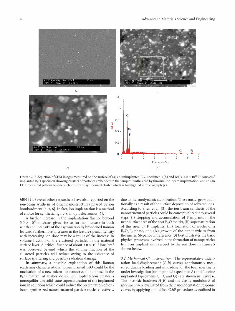
The SEM and EDX analysis of the heavily implantedspecimen (B4 in Figures 2(b)–2(d)), for example, showsobvious dissimilarities between the unimplanted and theimplanted specimen. Firstly, in addition to the homogeneousB6O phase the surface pores and the iron and chromiumcontamination, SEM micrographs show evidence of the
existence of additional clusters of ion-beam-synthesizedparticles. Secondly, image analysis of the microstructure(Figures 2(b) and 2(c)) indicates that the average particlesizes of the formed clusters is 110 nm. Thirdly, the measuredEDX pattern shows two weak iron peaks at 0.75 ev and6.4 eV. Although the positions of the 0.75 eV iron peak andthe fluorine peak coincide, there appears to exist enoughevidence observed to indicate a BxOyFz stoichiometry forthe ion-beam-synthesized clustered particles. We have alsoobserved that the compositional change becomes more sig-nificant with increasing fluorine implantation dose. The B6Osignature EDX pattern unimplanted specimen is depicted inFigure 1(b) [15, 28].
3.1.3. Raman Spectroscopy Analysis. Raman scattering spec-troscopy is very sensitive to the nature of crystalline struc-ture, disorder, and amorphization and is often employedto characterize ion-implantation-induced defects and anyirregularity in the crystalline symmetry. The rather populartechnique offers a rapid, nondestructive, and simple diagnos-tic probe for the evaluation of the structural modificationsimposed by ion implantation and for optical characterizationof ion-implanted specimens since the penetration depthof the laser beam is often of the order of the depth ofpenetration of implanted ions.
Figures 3 and 4 show the Raman spectra of pristine(specimen A) and F+-implanted hot-pressed B6O (specimensB to G). The Raman spectrum of the pristine specimen ischaracteristic of nominal composition B6O [21, 29–32].
The measured Raman spectra are evidently characterizedby a relatively low Raman signal to noise ratio. Nevertheless,it is not difficult to see that F+ implantation at fluences upto 5.0× 10¹⁵ ions/cm2 reveals that the material resists amor-phization and retains the crystal structure of B6O. At thesame time, implantation at fluences above 5.0×10¹⁵ ions/cm2
clearly shows that the signature Raman spectrum of B6Opredominately disappears (specimen D).
Rao et al. [33, 34], in Raman scattering spectroscopy,the main effect in going from the crystalline to amorphousform is the introduction of characteristic features in thefrequencies and line shapes of the Raman modes. However,for a diatomic lattice, the effect of amorphization shouldbe a decrease in intensity of the lattice modes and even thedisappearance of these modes at higher ion implantationdoses. Accordingly, we tentatively attribute the disappearanceof the signature B6O Raman spectrum at implantationfluences exceeding 5.0 × 10¹⁵ ions/cm2 to amorphization asa result of ion-induced radiation damage.
Measured spectra on samples implanted at fluencesbeyond 5.0 × 10¹⁵ ions/cm2 reveal an almost unrelatedand new asymmetrically broadened Raman feature centredaround 1550 cm−1. In general, it is widely accepted in thefield that the observed line shape asymmetry is consistentwith the size-dependent effects in measured Raman modes—optical phonon confinement [35]. The existence of ion-beam-synthesized aggregates made up of micro- and/ornanosized particles is known to exhibit this phenomenon.For example, we recently reported on the Raman spectraof cBN nanocrystals formed by He+ ion implantation into
4 Advances in Materials Science and Engineering
Acc. V Det WD2000x CL
10μm512 kV 11.9Spot Magn
B6O
(a)
1μmAcc. V Det WD20000x SE515 kV 12.6
Spot MagnB6O-B4
(b)
Acc. V Det WD 500 nm40000x SE 12.6515 kV
Spot MagnB6O-B4
(c)
0 1 2 3 4 5 6 70
0.2
0.5
0.7
1
1.2
KC
nt
Energy (keV)
B
O
Fe
FeCr
F
(d)
Figure 2: A depiction of SEM images measured on the surface of (a) an unimplanted B6O specimen, ((b) and (c)) a 5.0× 10¹⁵ F+ ions/cm2
implanted B6O specimen showing clusters of particles embedded in the samples synthesized by fluorine-ion-beam implantation, and (d) anEDX measured pattern on one such ion-beam-synthesized cluster which is highlighted in micrograph (c).
hBN [9]. Several other researchers have also reported on theion-beam synthesis of other nanostructures phased by ionbombardment [3, 5, 6]. In fact, ion implantation is a methodof choice for synthesizing nc-Si in optoelectronics [7].
A further increase in the implantation fluence beyond5.0 × 1015 ions/cm2 gives rise to further increase in bothwidth and intensity of the asymmetrically broadened Ramanfeature. Furthermore, increases in the feature’s peak intensitywith increasing ion dose may be a result of the increase involume fraction of the clustered particles in the materialsurface layer. A critical fluence of about 3.0 × 10¹⁶ ions/cm2
was observed beyond which the volume fraction of theclustered particles will reduce owing to the existence ofsurface sputtering and possibly radiation damage.
In summary, a possible explanation of this Ramanscattering characteristic in ion-implanted B6O could be thenucleation of a new micro- or nanocrystalline phase in theB6O matrix. At higher doses, ion implantation creates anonequilibrium solid-state supersaturation of the implantedions in solutions which could induce the precipitation of ion-beam-synthesized nanostructured particle nuclei effectively,
due to thermodynamic stabilization. These nuclei grow addi-tionally as a result of the surface deposition of solvated ions.According to Shen et al. [8], the ion beam synthesis of thenanostructured particles could be conceptualized into severalsteps: (i) stopping and accumulation of F implants in thenear-surface area of the host B6O matrix, (ii) supersaturationof this area by F implants, (iii) formation of nuclei of aBxOyFz phase, and (iv) growth of the nanoparticles fromthe nuclei. Stepanov in reference [3] best illustrates the basicphysical processes involved in the formation of nanoparticlesfrom an implant with respect to the ion dose in Figure 5shown below.
3.2. Mechanical Characterization. The representative inden-tation load-displacement (P-h) curves continuously mea-sured during loading and unloading for the four specimensunder investigation (unimplanted (specimen A) and fluorineimplanted (specimens C, D, and G)) are shown in Figure 6.The intrinsic hardness H(E) and the elastic modulus E ofspecimen were evaluated from the nanoindentation responsecurves by applying a modified O&P procedure as outlined in

Advances in Materials Science and Engineering 5
First-order R.S. Higher-order R.S.
500 1000 1500 2000 2500
Raman shift (cm− 1)
Ram
anin
ten
sity
(a.u
.)
Incr
easi
ng
F+io
ndo
se
A
B
C
D
E
F
G
Figure 3: The Raman spectra of unimplanted (specimen A) andfluorine-ion-implanted (specimens B to G) B6O specimen. Thespectra are shifted along the y-axis for better comparison. The y-axis is normalized.
1000 1250 1500 1750
Raman shift (cm− 1)
Ram
anin
ten
sity
(a.u
.)
A
B
C
D
E
F
G
Figure 4: An expanded view of the normalized Raman spectraof the 1550 cm−1 mode. A comparison between measured (dottedcurve) and calculated first-order Raman line shapes of ion-implanted B6O. Again, the y-axis is normalized, and the spectra areshifted along the y-axis for better comparison.
Appendix A [37–39]. The AFM imaging of the indentationimpressions and analysis has been relegated to Appendix B.An average surface roughness (determined from the AFMimages, see Figure 9) of about 7 nm Ra measured on thesurface appears to be a very small fraction of the maximumindentation depth and does not appear to influence themechanical properties significantly. Table 2 shows a sum-mary of the calculated values of H(E) and E, as well as the
1016 ion/cm2 1017 ion/cm2 Ion dose
Ion implantation Laser or thermal annealing
Sputtering
Substrate
Supersaturation Nucleation Growth Ostwald ripening Coalescence
Figure 5: An illustration of the basic physical processes (from leftto right) involved in the formation of clustered particles from animplant with respect to the ion dose. Surface sputtering underirradiation is also considered [36]. Diagram courtesy of Stepanov[3]. Note. In this study, all characterization was done on as-implanted specimen; no annealing was done.
Specimen ASpecimen C
Specimen DSpecimen G
0 100 200 300 400 500 600
Penetration depth, h (nm)
0
20
40
60
80
100
Load
,P(m
N)
Hot-pressed boron suboxide
Figure 6: Representative indentation response curves measuredduring the nanoindentation measurements on the unimplanted(specimen A), and fluorine-implanted (specimen C, D, and G) hot-pressed boron suboxide specimen.
Table 2: A summary of the effect of ion implantation on H(E), E,the ratio H/E, and the Meyer’s index n.
SpecimenH(E) E
H/E nGPa GPa
A 31.0 328.0 0.093 1.66
C 29.0 359.0 0.082 1.92
D 23.0 300.0 0.076 1.94
G 21.0 292.0 0.073 1.96
ratio H/E and the Meyer’s index, n (see (1) below), alsocalculated from the experimentally measured loading P-hcurves.
In order to exhibit all dependences (of the mechanicalproperties on the fluence of implantation) in one figure for
6 Advances in Materials Science and Engineering
0 25 50 425 450 475 500
0.7
0.8
0.9
1
Hardness, H (E)
Nor
mal
ized
har
dnes
s
Fluence (× 1014 F+/cm2)
(a) Intrinsic hardness
0 25 50 425 450 475 500
0.9
1
1.1
Elastic modulus, E
Ela
stic
mod
ulu
s
Fluence (× 1014 F+/cm2)
(b) Elastic modulus
0 25 50 425 450 475 500
0.8
0.9
1
H/E ratio
H/E
rati
o
Fluence (× 1014 F+/cm2)
(c) H/E ratio
0 25 50 425 450 475 5001.6
1.7
1.8
1.9
2
Mey
ers
inde
x
Meyer s index, n
Fluence (× 1014 F+/cm2)
(d) The Meyer’s index measured for hot-pressed B6O samples irradi-ated with various fluences of F ions
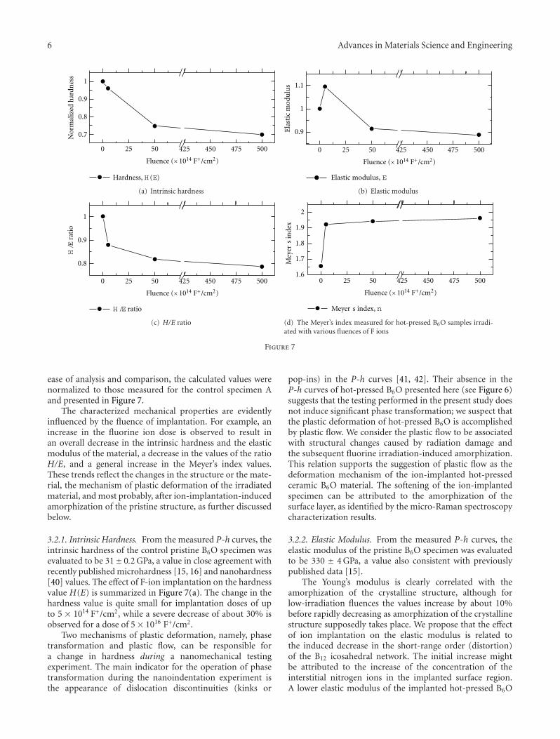
Figure 7
ease of analysis and comparison, the calculated values werenormalized to those measured for the control specimen Aand presented in Figure 7.
The characterized mechanical properties are evidentlyinfluenced by the fluence of implantation. For example, anincrease in the fluorine ion dose is observed to result inan overall decrease in the intrinsic hardness and the elasticmodulus of the material, a decrease in the values of the ratioH/E, and a general increase in the Meyer’s index values.These trends reflect the changes in the structure or the mate-rial, the mechanism of plastic deformation of the irradiatedmaterial, and most probably, after ion-implantation-inducedamorphization of the pristine structure, as further discussedbelow.
3.2.1. Intrinsic Hardness. From the measured P-h curves, theintrinsic hardness of the control pristine B6O specimen wasevaluated to be 31± 0.2 GPa, a value in close agreement withrecently published microhardness [15, 16] and nanohardness[40] values. The effect of F-ion implantation on the hardnessvalue H(E) is summarized in Figure 7(a). The change in thehardness value is quite small for implantation doses of upto 5 × 10¹⁴ F+/cm2, while a severe decrease of about 30% isobserved for a dose of 5× 10¹⁶ F+/cm2.
Two mechanisms of plastic deformation, namely, phasetransformation and plastic flow, can be responsible fora change in hardness during a nanomechanical testingexperiment. The main indicator for the operation of phasetransformation during the nanoindentation experiment isthe appearance of dislocation discontinuities (kinks or
pop-ins) in the P-h curves [41, 42]. Their absence in theP-h curves of hot-pressed B6O presented here (see Figure 6)suggests that the testing performed in the present study doesnot induce significant phase transformation; we suspect thatthe plastic deformation of hot-pressed B6O is accomplishedby plastic flow. We consider the plastic flow to be associatedwith structural changes caused by radiation damage andthe subsequent fluorine irradiation-induced amorphization.This relation supports the suggestion of plastic flow as thedeformation mechanism of the ion-implanted hot-pressedceramic B6O material. The softening of the ion-implantedspecimen can be attributed to the amorphization of thesurface layer, as identified by the micro-Raman spectroscopycharacterization results.
3.2.2. Elastic Modulus. From the measured P-h curves, theelastic modulus of the pristine B6O specimen was evaluatedto be 330 ± 4 GPa, a value also consistent with previouslypublished data [15].
The Young’s modulus is clearly correlated with theamorphization of the crystalline structure, although forlow-irradiation fluences the values increase by about 10%before rapidly decreasing as amorphization of the crystallinestructure supposedly takes place. We propose that the effectof ion implantation on the elastic modulus is related tothe induced decrease in the short-range order (distortion)of the B12 icosahedral network. The initial increase mightbe attributed to the increase of the concentration of theinterstitial nitrogen ions in the implanted surface region.A lower elastic modulus of the implanted hot-pressed B6O

Advances in Materials Science and Engineering 7
Table 3: H/E ratios of B6O and hard ceramic materials.
Material H/E ratio
Diamond 0.09–0.1 [44]
Hot-pressed B6O 0.093
B4C 0.07–0.09 [44]
SiC 0.080 [44]
Si3N4 0.080 [44]
Silicon 0.062 [46]
could be associated with the implantation-induced increasein the B–B bond angle deviations or simply the collectivedistortion of the individual B12 icosahedra or/and the α-rhombohedral framework, as a result of ion bombardment(see Figure 7(b)); it is well accepted that material havingcrystalline phases has a higher modulus than the materialswith amorphous structure [43]. This is an observation whichcorrelates well with the measured Raman results discussed inthis paper (Figure 3).
3.2.3. H/E Ratio. The ratio of H(E) to E, (H/E) is known asthe rigidity index, a key parameter in determining the type ofbehaviour observed in nanoindentation and nanoscratchingwear [44–46]. The ratio H/E can be regarded as a tool todescribe, rank, or calculate values for performance criteriawhich are important in defining the wear resistance of amaterial, such as the elastic strain to failure, the critical yieldpressure for plastic deformation, and the fracture toughness.A high H/E ratio is often a reliable indicator of good wearresistance in a coating or layers [45, 47].
The pristine specimen shows a higher H/E ratio whencompared to that of the implanted samples (refer toFigure 7(c)). This implies that F ion implantation of the B6Osurface at a larger fluence is expected to cause a considerableincrease in the surface plasticity. The experimental slidingwear test data is not available at present. However, usingthis rigidity index approximation, we suspect that the wearresistance from the ion-irradiated surfaces is expected todegrade at a larger fluences of implantation.
The intrinsic hardness clearly correlates very well withthe H/E ratio; this is no coincidence since hardness (or theplasticity) is known to have the decisive role of the surfacelayer on friction properties [45, 46].
A comparison of the H/E ratio of hot-pressed B6O withother ultrahard ceramic materials is shown in Table 3.
3.2.4. Meyer’s Index. To date, there exists immense experi-mental and theoretical evidence suggesting that, for someceramic materials, the evaluated hardness value is not amaterial constant but rather a function of either the appliedtest load or the depth of the indentation—the indentationsize effect (ISE) [48–52]. Several studies have reported thatMeyer’s law is sufficient to indicate the existence of ISE,although considered inadequate when describing the originsof ISE [48, 50]. The classic power law relationship shown in(1) is commonly known as Meyer’s law:
P = A · hn. (1)
Both A and n are constants for a particular sample. Thedescriptive parameters are usually deduced by a suitableregression analysis of the experimental load-displacementrelations for the loading segment.
The parameter n is also known as the size-effect index. Itis usually considered as a measure of ISE [50, 52]. The Meyerindex has been experimentally observed to be between 1.5and 2.0 for ceramics [48]. For the normal ISE behaviour,the exponent n < 2—the measured hardness apparentlydecreases with increasing applied test load. When n > 2, thereis the reverse ISE behaviour. When n = 2, the hardness isindependent of the applied test load.
In this study ISE curves were modelled on the basis of theMeyer’s model [50, 53]. Figure 7(d) shows an increase in nwith the increasing ion dose of fluorine ions. In other words,there is a point to make at higher doses where n → 2; itappears there is the diminishing evidence of indentation sizeeffects in hardness with increasing fluorine ion doses, and asingle hardness value for the material exists.
4. Conclusions
The following conclusions are obtained from this study.
(i) For F+ implantation at fluences below 5.0 × 10¹⁵
ions/cm2 the hot-pressed B6O samples resist amor-phization and retain the B6O crystal structure.However, for fluences above 5.0 × 10¹⁵ ions/cm2,the signature Raman spectrum of B6O disappears.Furthermore, beyond 5.0×10¹⁵ ions/cm2, the Ramanspectra appear to reveal that the fluorine implants inB6O matrix could influence the precipitation of ion-beam-synthesized clusters of a BxOyFz phase.
(ii) AFM and SEM images complement the Ramanspectroscopy results on the existence of agglomeratedion-beam-synthesized clustered particles on the ion-implanted specimen surface. Although not conclu-sive, the EDX compositional analysis hints that theclustered particles have a BxOyFz stoichiometry. Theexact structure and stoichiometry of the new phaseare yet to be determined.
(iii) In general, fluorine implantation of the specimenleads to an overall decrease in the intrinsic hardnessand the elastic modulus of the material. Thesetrends reflect on the changes in the structure orthe material, the mechanism of plastic deformationof the irradiated material, and most probably, ion-implantation-induced amorphization of the pristinestructure.
(a) This relation tentatively supports the sugges-tion that plastic flow is the main deforma-tion mechanism in ion-implanted hot-pressedceramic B6O material. The softening of the ion-implanted specimen can be attributed to theamorphization of the surface layer, as identifiedby the micro-Raman spectroscopy characteriza-tion results.

8 Advances in Materials Science and Engineering
(iv) The decrease in both the H/E ratio and the Meyer’sindex with ion dose might imply that F ion implan-tation of the B6O surface at a larger fluence isexpected to cause a considerable increase in thesurface plasticity.
Appendices
A. Oliver and Pharr Analysis Approach
The nanoindentation technique has been established as apowerful means of characterizing the near-surface mechan-ical properties of materials [54]. This technique relies onhigh-resolution instruments that simultaneously measurethe load P and indenter displacements h, during the loadingand unloading indentation steps. The important parametersobtained from the resultant P-h curve, which are schemat-ically illustrated in Figure 8, are the peak load Pmax, themaximum penetration depth hmax, final penetration depthh f , and the contact stiffness S. The indentation analysisprocedure developed by Oliver and Pharr (O&P) has beenwidely used for hard materials such as metals and ceramics[38, 39, 54].
The O&P method makes use of the data taken from theupper portion of the unloading curve fitted with the power-law relation given as
P = α ·(h− h f
)m, (A1)
where m, the displacement exponent in the load-displacement relation and a, an unloading fitting parameterdependent on the elastic response of the material, areempirical constants to be determined using the power fittingof unloading data [49].
The derivative of P (A1) with respect to h yields thecontact stiffness S, which is the initial unloading slope of theP-h curve:
S =(dP
dh
)unloading
= m · α ·(h− h f
)m−1.
(A2)
The contact depth of the indent impression hc can either bederived by extrapolating the initial slope of the unloadingP-h curve down to P = 0 or otherwise determined using anempirical formula as observed by Oliver and Pharr [38, 39]given by
hc = hmax − ε · Pmax
S, (A3)
where, in this case for the Berkovich indenter geometry, ε =0.75 [38].
The contact area Ac is the cross-sectional area at hc [55,56]. Various experimental [56] and numerical [57] studieshave established that, for the Berkovich indenter geometry,
Pmax
hmaxhchf
Loading
UnloadingSLo
ad,P
Displacement, h
Figure 8: A typical load-displacement curve during a loading-unloading cycle where hmax is the maximum indenter displacementat peak indentation load Pmax, S is the initial unloading slope of theload-displacement curve, and hc is the contact depth.
the projected Ac can be approximated by the empiricalformula:
Ac(hc) =(
24.56 · h2c + C1 · h1/2
c + C2 · h1/4c
+C3 · h1/8c + · · · + C8 · h1/125
c
),
(A4)
where C1,C2, . . . ,C8 are constants determined by curve-fitting procedures [55, 56] and are all defined based onthe indenter tip radius [49]. However, for the Berkovichindenter geometry, projected area can be reduced toAc(hc) ≈24.56 · h2
c without compromising the accuracy of the results[54, 55, 58].
When S and Ac have been determined, the specimen’selastic modulus Es or simply E can then be evaluated using
1Er= 1− ν2
s
Es+
1− ν2i
Ei, (A5)
where νs and νi are, respectively, the specimen and indenterPoisson ratios, Ei is the indenter elastic modulus [54, 58], andEr is the reduced elastic modulus given by
Er =√π
2β· S√
Ac, (A6)
where β is a correctional factor introduced by King [59] toaddress the lack of indenter symmetry; for the Berkovichindenter β = 1.034 [58].
The indentation hardness H has long been defined as thetest force P divided by the projected area of contact Ac [60]:
H = Pmax
Ac. (A7)
Advances in Materials Science and Engineering 9
x: 3.8μm y: 3.8μm
2.59μm2.36μm
(a) Specimen A
x: 3.3μm y: 3.3μm
2.7μm2.38μm
(b) Specimen C
x: 4μmy: 4μm
2.78μm2.41μm
(c) Specimen D
x: 4.4μmy: 4.4μm
2.79μm2.38μm
(d) Specimen G
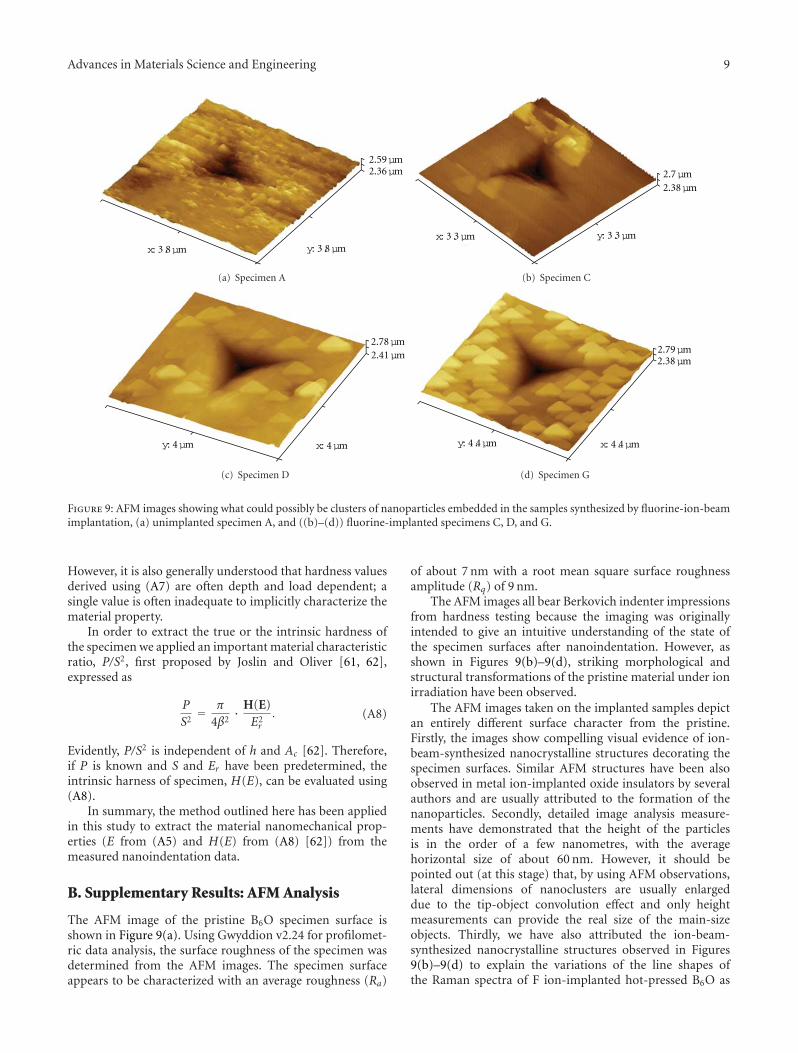
Figure 9: AFM images showing what could possibly be clusters of nanoparticles embedded in the samples synthesized by fluorine-ion-beamimplantation, (a) unimplanted specimen A, and ((b)–(d)) fluorine-implanted specimens C, D, and G.
However, it is also generally understood that hardness valuesderived using (A7) are often depth and load dependent; asingle value is often inadequate to implicitly characterize thematerial property.
In order to extract the true or the intrinsic hardness ofthe specimen we applied an important material characteristicratio, P/S2, first proposed by Joslin and Oliver [61, 62],expressed as
P
S2= π
4β2· H(E)
E2r
. (A8)
Evidently, P/S2 is independent of h and Ac [62]. Therefore,if P is known and S and Er have been predetermined, theintrinsic harness of specimen, H(E), can be evaluated using(A8).
In summary, the method outlined here has been appliedin this study to extract the material nanomechanical prop-erties (E from (A5) and H(E) from (A8) [62]) from themeasured nanoindentation data.
B. Supplementary Results: AFM Analysis
The AFM image of the pristine B6O specimen surface isshown in Figure 9(a). Using Gwyddion v2.24 for profilomet-ric data analysis, the surface roughness of the specimen wasdetermined from the AFM images. The specimen surfaceappears to be characterized with an average roughness (Ra)
of about 7 nm with a root mean square surface roughnessamplitude (Rq) of 9 nm.
The AFM images all bear Berkovich indenter impressionsfrom hardness testing because the imaging was originallyintended to give an intuitive understanding of the state ofthe specimen surfaces after nanoindentation. However, asshown in Figures 9(b)–9(d), striking morphological andstructural transformations of the pristine material under ionirradiation have been observed.
The AFM images taken on the implanted samples depictan entirely different surface character from the pristine.Firstly, the images show compelling visual evidence of ion-beam-synthesized nanocrystalline structures decorating thespecimen surfaces. Similar AFM structures have been alsoobserved in metal ion-implanted oxide insulators by severalauthors and are usually attributed to the formation of thenanoparticles. Secondly, detailed image analysis measure-ments have demonstrated that the height of the particlesis in the order of a few nanometres, with the averagehorizontal size of about 60 nm. However, it should bepointed out (at this stage) that, by using AFM observations,lateral dimensions of nanoclusters are usually enlargeddue to the tip-object convolution effect and only heightmeasurements can provide the real size of the main-sizeobjects. Thirdly, we have also attributed the ion-beam-synthesized nanocrystalline structures observed in Figures9(b)–9(d) to explain the variations of the line shapes ofthe Raman spectra of F ion-implanted hot-pressed B6O as

10 Advances in Materials Science and Engineering
shown in Figure 3 and reference [14]. Fourthly and lastly,the surfaces of the implanted samples appear to be muchsmoother in appearance than those of the pristine sample[63], tentatively suggestive that possible sputtering andother dynamic processes could have influenced the surfacemorphology of the specimen during implantation.
Acknowledgments
The authors are appreciative for the valuable contributionsof O. T. Johnson, M. Herrmann, W. Goosen, J. Neethling,the Nelson Mandela Metropolitan University, and the Centrefor Scientific and Industrial Research’s National Centre forNanostructured Materials. The financial support from theDST/NRF Centre of Excellence in Strong Materials andUniversity of the Witwatersrand Mellon Postgraduate Awardis also gratefully acknowledged.
References
[1] K. J. Kirkby and R. P. Webb, “Ion Implanted Nanostructures,”in Encyclopedia of Nanoscience and Nanotechnology, H. S.Nalwa, Ed., vol. 4, pp. 1–11, American Scientific Publishers,2004.
[2] I. Jain and G. Agarwal, “Ion beam induced surface andinterface engineering,” Surface Science Reports, vol. 66, no. 3-4,pp. 77–172, 2011.
[3] A. L. Stepanov, “Synthesis of silver nanoparticles in dielectricmatrix by ion implantation: a review,” Reviews on AdvancedMaterials Science, vol. 26, no. 1-2, pp. 1–29, 2010.
[4] J. F. Prins, “Modification, doping and devices in implanteddiamond,” in Properties of Natuaral and Synthetic Diamong,chapter 8, pp. 301–341, Academic Press Limited, 1992.
[5] J. Ghatak, B. Satpati, M. Umananda et al., “Characterizationof ion beam induced nanostructures,” Nuclear Instruments andMethods in Physics Research B, vol. 244, no. 1, pp. 45–51, 2006.
[6] D. K. Avasthi and J. C. Pivin, “Ion beam for synthesis andmodification of nanostructures,” Current Science, vol. 98, no.6, pp. 780–792, 2010.
[7] H. Hosono and H. Kawazoe, “Approach to novel crystallineand amorphous oxide materials for optoelectronics by ionimplantation,” Materials Science and Engineering B, vol. 41, no.1, pp. 39–45, 1996.
[8] Y. Shen, X. Li, Z. Wang et al., “Fabrication and thermalevolution of nanoparticles in SiO2 by Zn ion implantation,”Journal of Crystal Growth, vol. 311, no. 21, pp. 4605–4609,2009.
[9] R. MacHaka, R. M. Erasmus, and T. E. Derry, “Formation ofcBN nanocrystals by He+ implantation into hBN,” Diamondand Related Materials, vol. 19, no. 10, pp. 1131–1134, 2010.
[10] I. D. Desnica-Frankovi, K. Furi, U. V. Desnica, M. C. Ridgway,and C. J. Glover, “Structural modifications in amorphousGe produced by ion implantation,” Nuclear Instruments andMethods in Physics Research B, vol. 178, no. 1–4, pp. 192–195,2001.
[11] T. W. H. Oates, L. Ryves, F. A. Burgmann et al., “Ionimplantation induced phase transformation in carbon andboron nitride thin films,” Diamond and Related Materials, vol.14, no. 8, pp. 1395–1401, 2005.
[12] F. Komarov, L. Vlasukova, W. Wesch et al., “Formation of InAsnanocrystals in Si by high-fluence ion implantation,” Nuclear
Instruments and Methods in Physics Research B, vol. 266, no.16, pp. 3557–3564, 2008.
[13] J. I. Onate, F. Alonso, and A. Garcıa, “Improvement oftribological properties by ion implantation,” Thin Solid Films,vol. 317, no. 1-2, pp. 471–476, 1998.
[14] R. Machaka, T. E. Derry, and I. Sigalas, “Nanoindentationhardness of hot-pressed boron suboxide,” Materials Scienceand Engineering A, vol. 528, no. 18, pp. 5778–5783, 2011.
[15] M. Herrmann, H. J. Kleebe, J. Raethel et al., “Field-assisteddensification of superhard B6O materials with Y2O3/Al2O3
addition,” Journal of the American Ceramic Society, vol. 92, no.10, pp. 2368–2372, 2009.
[16] M. Herrmann, J. Raethel, A. Bales, K. Sempf, I. Sigalas, and M.Hoehn, “Liquid phase assisted densification of superhard B6Omaterials,” Journal of the European Ceramic Society, vol. 29, no.12, pp. 2611–2617, 2009.
[17] O. T. Johnson, I. Sigalas, E. N. Ogunmuyiwa, H. J. Kleebe, M.M. Muller, and M. Herrmann, “Boron suboxide materials withCo sintering additives,” Ceramics International, vol. 36, no. 6,pp. 1767–1771, 2010.
[18] A. Andrews, M. Herrmann, T. C. Shabalala, and I. Sigalas,“Liquid phase assisted hot pressing of boron suboxide-materials,” Journal of the European Ceramic Society, vol. 28, no.8, pp. 1613–1621, 2008.
[19] A. Andrews, Development of boron suboxide composites withimproved toughness, Ph.D. thesis, School of Chemical andMetallurgical Engineering, University of the Witwatersrand0,2009.
[20] C. S. Freemantle, The wear studies of boron suboxide basedcutting tool materials in machining applications, M.S. thesis,School of Chemical and Metallurgical Engineering, Universityof the Witwatersrand, 2010.
[21] R. Machaka, B. W. Mwakikunga, E. Manikandan, T. E.Derry, and I. Sigalas, “Raman spectrum of hot-pressed boronsuboxide,” Advanced Materials Letters, vol. 2, p. 68, 2011.
[22] J. Lowther, Personal Communication, 2009.
[23] J. F. Prins, “Ion-implanted structures and doped layers indiamond,” Materials Science Reports, vol. 7, no. 7-8, pp. 271–364, 1992.
[24] J. Ziegler, SRIM2010 (Software package), 2010, http://www.srim.org/.
[25] P. Klapetek, D. Necas, and C. Anderson, Gwyddion v2.24(Software package), 2010, http://gwyddion.net/.
[26] R. Machaka, B. W. Mwakikunga, E. Manikandan, T. E. Derry,and I. Sigalas, “Structural transformation in ultrahard B6Oinduced by F-ion implantation studied by micro-Ramanspectroscopy,” Unpublished.
[27] O. T. Johnson, Improvement on the mechanical properties ofboron suboxide (B60) based composites using other compoundsas second phase, M.S. thesis, School of Chemical and Metallur-gical Engineering, University of the Witwatersrand, 2009.
[28] O. T. Johnson, I. Sigalas, and M. Herrmann, “Microstructureand interfacial reactions between B6O and (Ni, Co) couples,”Ceramics International, vol. 36, no. 8, pp. 2401–2406, 2010.
[29] Z. Wang, Y. Zhao, P. Lazor, H. Annersten, and S. K. Saxena, “Insitu pressure Raman spectroscopy and mechanical stability ofsuperhard boron suboxide,” Applied Physics Letters, vol. 86, no.4, Article ID 041911, pp. 1–41911, 2005.
[30] H. Werheit and U. Kuhlmann, “FTIR and FT Raman spectraof B6O,” Journal of Solid State Chemistry, vol. 133, no. 1, pp.260–263, 1997.
Advances in Materials Science and Engineering 11
[31] S. Yu, Y. Ji, T. Li et al., “Nanofilms with clusters of boronsuboxide and their infrared absorption,” Solid State Commu-nications, vol. 115, no. 6, pp. 307–311, 2000.
[32] V. L. Solozhenko, O. O. Kurakevych, and P. Bouvier, “Firstand second-order Raman scattering of B6O,” Journal of RamanSpectroscopy, vol. 40, no. 8, pp. 1078–1081, 2009.
[33] C. S. R. Rao, S. Sundaram, R. L. Schmidt, and J. Comas,“Study of ion-implantation damage in GaAs:Be and InP:Beusing Raman scattering,” Journal of Applied Physics, vol. 54,no. 4, pp. 1808–1815, 1983.
[34] S. S. Kumar, M. A. Khadar, S. K. Dhara, T. R. Ravindran, andK. G. M. Nair, “Photoluminescence and Raman studies of ZnSnanoparticles implanted with Cu+ ions,” Nuclear Instrumentsand Methods in Physics Research B, vol. 251, no. 2, pp. 435–440,2006.
[35] A. K. Arora, M. Rajalakshmi, T. R. Ravindran, and V.Sivasubramanian, “Raman spectroscopy of optical phononconfinement in nanostructured materials,” Journal of RamanSpectroscopy, vol. 38, no. 6, pp. 604–617, 2007.
[36] M. Nastasi and J. W. Mayer, Ion Implantation and Synthesis ofMaterials, Springer, Berlin, Germany, 2006.
[37] W. C. Oliver and G. M. Pharr, “Improved technique fordetermining hardness and elastic modulus using load anddisplacement sensing indentation experiments,” Journal ofMaterials Research, vol. 7, no. 6, pp. 1564–1580, 1992.
[38] W. C. Oliver and G. M. Pharr, “Measurement of hardnessand elastic modulus by instrumented indentation: advancesin understanding and refinements to methodology,” Journal ofMaterials Research, vol. 19, no. 1, pp. 3–20, 2004.
[39] G. M. Pharr and A. Bolshakov, “Understanding nanoindenta-tion unloading curves,” Journal of Materials Research, vol. 17,no. 10, pp. 2660–2671, 2002.
[40] X. Jiao, H. Jin, F. Liu et al., “Synthesis of boron suboxide (B6O)with ball milled boron oxide (B2O3) under lower pressure andtemperature,” Journal of Solid State Chemistry, vol. 183, no. 7,pp. 1697–1703, 2010.
[41] S. R. Jian, G. J. Chen, and J. Y. Juang, “Nanoindentation-induced phase transformation in (1 1 0)-oriented Si single-crystals,” Current Opinion in Solid State and Materials Science,vol. 14, no. 3-4, pp. 69–74, 2010.
[42] C. A. Schuh, “Nanoindentation studies of materials,” MaterialsToday, vol. 9, no. 5, pp. 32–40, 2006.
[43] J. G. Wang, B. W. Choi, T. G. Nieh, and C. T. Liu,“Crystallization and nanoindentation behavior of a bulk Zr-Al-Ti-Cu-Ni amorphous alloy,” Journal of Materials Research,vol. 15, no. 3, pp. 798–807, 2000.
[44] N. Laidania, A. Miotello, and J. Perriere, “Chemical, mechani-cal and electrical properties of CNx-films produced by reactivesputtering and N+-implantation in carbon films,” AppliedSurface Science, vol. 99, no. 4, pp. 273–284, 1996.
[45] A. Leyland and A. Matthews, “On the significance of the H/Eratio in wear control: a nanocomposite coating approach tooptimised tribological behaviour,” Wear, vol. 246, no. 1-2, pp.1–11, 2000.
[46] P. Lemoine, J. P. Quinn, P. Maguire, and J. A. McLaughlin,“Comparing hardness and wear data for tetrahedral amor-phous carbon and hydrogenated amorphous carbon thinfilms,” Wear, vol. 257, no. 5-6, pp. 509–522, 2004.
[47] T. Oberle, “Properties influencing the wear of metals,” Journalof Metrologia, vol. 3, p. 438, 1951.
[48] J. Gong, J. Wu, and Z. Guan, “Analysis of the indentationsize effect on the apparent hardness for ceramics,” MaterialsLetters, vol. 38, no. 3, pp. 197–201, 1999.
[49] J. Gong, H. Miao, and Z. Peng, “A new function for thedescription of the nanoindentation unloading data,” ScriptaMaterialia, vol. 49, no. 1, pp. 93–97, 2003.
[50] O. Sahin, O. Uzun, U. Kolemen, and N. Ucar, “Mechanicalcharacterization for β-Sn single crystals using nanoindenta-tion tests,” Materials Characterization, vol. 59, no. 4, pp. 427–434, 2008.
[51] O. Sahin, O. Uzun, M. Sopicka-Lizer, H. Gocmez, and U.Kolemen, “Dynamic hardness and elastic modulus calculationof porous SiAlON ceramics using depth-sensing indentationtechnique,” Journal of the European Ceramic Society, vol. 28,no. 6, pp. 1235–1242, 2008.
[52] K. Sangwal, “On the reverse indentation size effect andmicrohardness measurement of solids,” Materials Chemistryand Physics, vol. 63, no. 2, pp. 145–152, 2000.
[53] H. Li and R. C. Bradt, “The indentation load/size effect andthe measurement of the hardness of vitreous silica,” Journal ofNon-Crystalline Solids, vol. 146, pp. 197–212, 1992.
[54] A. Fischer-Cripps, Nanoindentation, Springer, New York, NY,USA, 2nd edition, 2004.
[55] J. Gong, H. Miao, and Z. Peng, “Analysis of the nanoinden-tation data measured with a Berkovich indenter for brittlematerials: effect of the residual contact stress,” Acta Materialia,vol. 52, no. 3, pp. 785–793, 2004.
[56] J. Gong, H. Miao, and Z. Peng, “On the contact area fornanoindentation tests with Berkovich indenter: case study onsoda-lime glass,” Materials Letters, vol. 58, no. 7-8, pp. 1349–1353, 2004.
[57] K. D. Bouzakis and N. Michailidis, “Indenter surface areaand hardness determination by means of a FEM-supportedsimulation of nanoindentation,” Thin Solid Films, vol. 494, no.1-2, pp. 155–160, 2006.
[58] N. Janakiraman and F. Aldinger, “Indentation analysis ofelastic and plastic deformation of precursor-derived Si-C-Nceramics,” Journal of the European Ceramic Society, vol. 30, no.3, pp. 775–785, 2010.
[59] R. B. King, “Elastic analysis of some punch problems for a lay-ered medium,” International Journal of Solids and Structures,vol. 23, no. 12, pp. 1657–1664, 1987.
[60] B. Mott, Microindentation Hardness Testing, Butterworths,London, UK, 1956.
[61] D. L. Joslin and W. C. Oliver, “New method for analyzingdata from continuos depth-sensing microindentation tests,”Journal of Materials Research, vol. 5, no. 1, pp. 123–126, 1990.
[62] X. Y. Zhou, Z. D. Jiang, H. R. Wang, and Q. Zhu, “A methodto extract the intrinsic mechanical properties of soft metallicthin films based on nanoindentation continuous stiffnessmeasurement technique,” Journal of Physics, vol. 48, no. 1,article 204, pp. 1096–1101, 2006.
[63] E. H. Lee, M. B. Lewis, P. J. Blau, and L. K. Mansur, “Improvedsurface properties of polymer materials by multiple ion beamtreatment,” Journal of Materials Research, vol. 6, no. 3, pp. 610–628, 1991.
Hindawi Publishing CorporationAdvances in Materials Science and EngineeringVolume 2012, Article ID 706094, 16 pagesdoi:10.1155/2012/706094
Research Article
Effect of Silicon, Titanium, and Zirconium IonImplantation on NiTi Biocompatibility
L. L. Meisner,1 A. I. Lotkov,1 V. A. Matveeva,2
L. V. Artemieva,2 S. N. Meisner,1 and A. L. Matveev2
1 Institute of Strength Physics and Materials Science, SB RAS, Akademichesky 2/4, Tomsk 634021, Russia2 Institute of Chemical Biology and Fundamental Medicine, SB RAS, Lavrent’eva 8, Novosibirsk 630090, Russia
Correspondence should be addressed to L. L. Meisner, [email protected]
Received 31 March 2011; Accepted 19 September 2011
Academic Editor: W. Ensinger
Copyright © 2012 L. L. Meisner et al. This is an open access article distributed under the Creative Commons Attribution License,which permits unrestricted use, distribution, and reproduction in any medium, provided the original work is properly cited.
The objective of the work was to study the effect of high-dose ion implantation (HDII) of NiTi surface layers with Si Ti, or Zr, on theNiTi biocompatibility. The biocompatibility was judged from the intensity and peculiarities of proliferation of mesenchymal stemcells (MSCs) on the NiTi specimen surfaces treated by special mechanical, electrochemical, and HDII methods and differing inchemical composition, morphology, and roughness. It is shown that the ion-implanted NiTi specimens are nontoxic to rat MSCs.When cultivated with the test materials or on their surfaces, the MSCs retain the viability, adhesion, morphology, and capabilityfor proliferation in vitro, as evidenced by cell counting in a Goryaev chamber, MTT test, flow cytometry, and light and fluorescencemicroscopy. The unimplanted NiTi specimens fail to stimulate MSC proliferation, and this allows the assumption of bioinertnessof their surface layers. Conversely, the ion-implanted NiTi specimens reveal properties favorable for MSC proliferation on theirsurface.
1. Introduction
Today, the treatment of ischemic heart disease (IHD) is stillone of the most urgent and foreground problems of theworld and national healthcare. Among modern methods ofIHD correction is intracoronary stenting [1, 2].
The treatment of a human vascular system with stents—endoprostheses—for increasing the lumen of vessels andkeeping them open requires application of materials withhigh strength and high elastoplastic characteristics. Alloysbased on titanium nickelide, or NiTi-based alloys, match infull measure the above requirements demonstrating supere-lasticity or so-called shape memory effect—the capability foraccumulation of high strain (4–6%) and its reversible returnwithout fracture [3–5].
Particular attention should be given to the surface treat-ment of endoprostheses. The surface of endoprostheses musthave minimum adhesion to preclude the risk of growth ofplain muscular tissue in the lumen of an implant whilstbeing biologically compatible and tolerable to medicineswith which the implant surface will contact.
It is apparent that for the biocompatibility of medicalmaterials to increase, it suffices to create or modify theproperties of their surface or thin surface layers. An efficientway of improving the physicochemical and mechanicalsurface characteristics of microsurgical tools, and increasingtheir biocompatibility is ion and electron beam surfacemodifications and a combination of these methods withdeposition of thin coatings made of biotolerable chemicalelements or composites [6, 7]. Surface conditioning of metalmaterials in several successive stages—etching, mechanicalgrinding and polishing, and electropolishing—is often finalfor implants. At the same time, this surface conditioning pre-cedes coating deposition or appropriate surface modificationand eventually determines the quality of a medical tool [8–10]. However, detailed data on the effect of the individualtreatment methods listed above or their combinations on theNiTi biocompatibility are scantily available.
A reliable method of preclinical biocompatibility assess-ment is testing of implant materials with cell cultures.In vitro testing allows us to study the action of a testmaterial on biological properties of mammalian cells. These
2 Advances in Materials Science and Engineering
examinations are conducted with CCL1, CCL 163, Vero,and other long-term cell lines, cultures of fibroblasts, lym-phocytes, macrophages, epithelial cells, and germ or diploidcells of humans and animals [11]. The choice of a stentmaterial is normally based on its examination with bloodcells, for example, for platelet adhesiveness to its surface.At the same time, the problem of long-term implantationeffects and possible growth of fibromuscular tissue on stentsurfaces requires examination of the surfaces on long-termcell cultures. Now, the properties of implants are studiedon mesenchymal stem cells (MSCs) [12] with their inherentdifferentiation of bone, connective, and muscular tissues in acell, and also on other mesodermal cells [13]. The capabilityof MSCs for proliferation in vitro [14] allows the use of MSCsin cytotoxicity assays of chemical compositions of implantsand analyses of their surface morphology. These studiesmake it possible to determine the conditions necessary forsuccessful cell proliferation, for example, in regeneration ofosseous defects [14] or vascular walls [15], and for maximumpossible surface resistance of a biocompatible material in cellproliferation.
The objective of the work is to study the biocompat-ibility of NiTi specimens treated by special mechanical,electrochemical, and HDII methods and their effect on theproliferation of mesenchymal stem cells and cytotoxicity.
2. Materials, Surface Treatment Methods,and Research Techniques
2.1. Materials and Surface Treatment Methods. The materialsto be tested were two series each of 80 flat-rolled specimensof commercial TiNi1 alloy (MATEKS, Russia). The NiTispecimens for physicochemical tests (14 specimens in aseries) and biological tests (66 specimens in a series) were flatplates of dimensions 1.6 × 10 × 15 mm3. For biological tests,the specimens were treated to have two types of surface—NiTi-A and NiTi-B.
Surface treatment A it included two steps:
Step 1. Etching in a solution (HNO3 and HF in a ratio of 3/1)heated to T = 50◦C for 3 min;
Step 2. Metallic-luster electropolishing in a solution(CH3COOH and HClO4 in a ratio of 3/1) cooled down toT =273 K (0◦C) at a voltage U = 30 V.
Surface treatment B it included three steps:
Step 1. Etching in a solution (HNO3 and HF in a ratio of 3/1)heated to T = 50◦C for 3 min;
Step 2. High-luster mechanical polishing on a Sapphirre 550grinder-polisher (ATM GMBH, Germany). The specimenswere placed in special metal cups, and the cups werefilled with epoxy resin and kept at room temperature (Tr)within a day for complete epoxy solidification. Thereafter,the specimens were grinded on silicon carbide grindingfoil (ATM GMBH, Germany) with a gradual decrease ingranularity from 100 to 1.2 ± 0.3 μm and supply of water
heated to T = 303 K (30◦C) to the grinding surface. Waterserved as a lubricant and simultaneously as a heater topreclude the appearance of a martensite phase in the process.The rate of rotation of the grinding table was v = 150 rpm;the grinding time for each level of granularity was Δt = 5–8 min (to the point of surface smoothening). At the finalstage, the specimens were polished on a polishing cloth alphaperforated paper with a Bio Diamant Cameo lubricant (LAMPLAN, France) of abrasivity 9 μm. The rate of rotation of thepolishing table was v = 150 rpm; the high-luster polishingtime was Δt = 2–5 min.
Step 3. Metallic-luster electropolishing in a solution(CH3COOH and HClO4 in a ratio of 3/1) cooled down toT =273 K (0◦C) at a voltage U = 30 V.
Ion implantation of the specimens was realized on aDIANA-3 (ISPMS SB RAS, Tomsk, Russia [16–18]) ionimplanter with Si, Ti, and Zr single-component pulsedion beams (using iodide Ti and Si cathodes) under theconditions of oilless pumping and high vacuum (∼10−6 Pa).This method is known as high-dose ion implantation (HDII)[19–22]. The ion beam treatment was in implantation ofNiTi surface layers with Si, Ti, or Zr ions of fluence D =2 × 1017 cm−2 at an average accelerating voltage of 60 kVand pulse repetition frequency of 50 Hz. The temperature ofthe specimens in ion implantation was no greater than 373–424 K. The specimens subjected to ion beam treatment wereNiTi-A and NiTi-B specimens differing in roughness suchthat for biological tests we prepared eight series of the NiTispecimens differing in chemical composition, topography,and roughness. The marking of the series of the specimenswith differently modified surfaces used in the work are givenin Table 1.
The investigations were made on the equipment of theShared Use Center (SUC) “Nanotech” of ISPMS SB RAS. Thesurface morphology was analyzed on the a LEO EVO 50 scan-ning electron microscope (Zeiss, Germany) and an Axiovert200 MAT optical microscope (Zeiss, Germany) with bright-and dark-field imaging and differential interference contrast(DIC) for visualization of objects with minimum differencesin surface roughness height. The phase composition of thespecimens was analyzed on a DRON-7 X-ray diffractometer(Burevestnik, Russia). Layer-by-layer elemental analysis wasperformed on a Shkhuna-2 Auger spectrometer (NR TPU,Russia). The diameter of a probing electron beam was∼1 μmand the electron energy was ∼3 keV. In recording of Augerspectra, the electron beam raster was 10 × 10 μm2. Theenergy resolution of the analyzer was 0.7%. The targetmaterial was sputtered layer by layer with an Ar ion beamof energy 3 keV and diameter 1 mm. The sputtering rate ofthe target material was 2-3 nm/min. Analysis of the surfaceroughness and surface treatment quality and visualizationof surface defects and fracture traces of the materials wasperformed on a New-View 5000 3D optical interferometer-profilometer (Zygo, USA) with a surface profile accuracy of±1 nm. The microhardness of surface layers of the specimenswas measured on a DM8 microhardness tester (Affri, Italy).

Advances in Materials Science and Engineering 3
Table 1: Types and description of surface treatment of the NiTi specimens.
Type of treatmentSubstrate material and type of
previous surface treatmentFinishing treatment Specimen marking
1 2 3 4
A NiTiStep 1: etching NiTi-A
Step 2: electropolishing
Step 1: etching
B NiTi Step 2: mechanical polishing NiTi-B
Step 3: electropolishing
GNiTi-A Step 4: HDII NiTi-AG
NiTi-B with Zr, DZr = 2 × 1017 cm−2 NiTi-BG
HNiTi-A Step 4: HDII NiTi-AH
NiTi-B with Ti, DTi = 2 × 1017 cm−2 NiTi-BH
JNiTi-A Step 4: HDII NiTi-AJ
NiTi-B with Si, DSi = 2 × 1017 cm−2 NiTi-BJ
Table 2: Doping element concentration in the ion-implanted surface layers and average surface roughness (roughness height parameter) ofthe NiTi specimens.
Type of treatment Specimen marking Ion type, fluenceDoping (implanted) concentration,
at. %Average roughness (roughness
height parameter) Ra, μm
A NiTi-AUnimplanted
— 0.972
B NiTi-B — 0.047–0.061
G NiTi-AG, Zr, >0.2 0.860–0.940
NiTi-BG D1 = 2 × 1017 cm−2 0.025–0.041
H NiTi-AH, Ti, >0.3 0.936–1.272
NiTi-BH D2 = 2 × 1017 cm−2 (relative to its concentration beforeirradiation)
0.026–0.035
J NiTi-AJ, Si, >0.58 0.892–0.921
NiTi-BJ D3 = 2 × 1017 cm−2 0.033–0.039
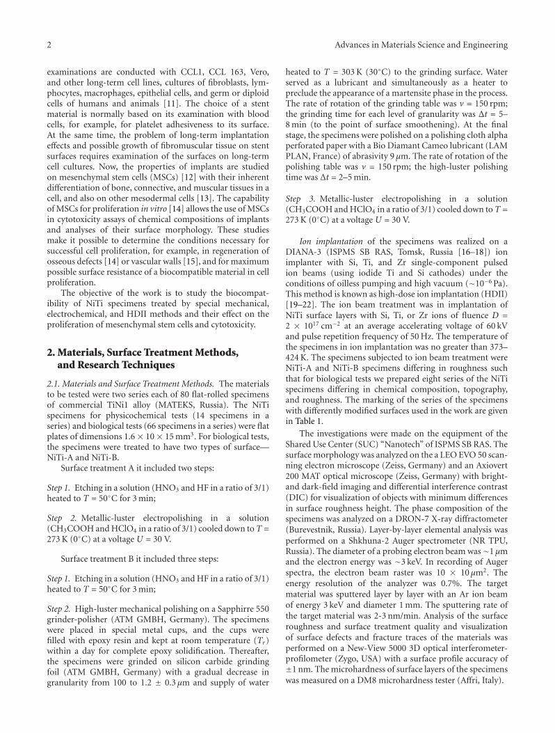
The specimens were examined in vitro on rat marrowmesenchymal stem cells of the 2nd passage. The cells werecultivated in an α-MEM medium containing 10% of fetalcalf serum, 200 mM of L-glutamine and 100 μg/mL ofgentamicin (Biolot, Russia) in 6- and 12-well plastic trays(Nunc, Denmark) at 37◦C in an atmosphere with 5% ofCO2 and with a saturation moisture content. In the tests,the specimens were in direct contact with the MSCs. Thecell viability was determined by cell counting in a Goryaevchamber according to [11] and in an MTS assay [23]according to [24].
The effect of the chemical composition and propertiesof the NiTi surface on the proliferation of MSCs cultivatedin vitro with the differently modified NiTi specimens wasdetermined from the characteristic properties of MSCs:proliferation and morphology [13]. The cytotoxic action ofthe specimens on rat marrow MSCs was estimated from theviability of the cells cultivated with the test specimens for72 h and 7 and 14 days. For this study, two types of tests wereperformed.
Test Type I. The cells were seeded into 6-well trays at a den-sity of 50 × 103 cell/cm2, and 24 hours later, the specimens
were placed in the wells and the cultivation was continued.After 72 hours, the cell viability was estimated throughcell counting in the Goryaev chamber and in the MTTtest (3-[4,5-dimethylthiazol-2-yl]-2,5-diphenyl tetrazoliumbromide). For cell counting in the Goryaev chamber, theattached cells were removed with a 0.25-% trypsin-EDTAsolution (Biolot, Russia) within 2–5 min. The cells werecounted in 150 large squares. For the MTT-test, the opticaldensity of eluate aliquots was measured on an Apollo-8 LB912 microplate photometer (Berthold Technologies, GmbHand Co, KG, Germany) in four iterations at a wavelength of620 and 570 nm to preclude the effect of cellular debris. Thecell viability was estimated in percent. Cell control wells werewells with no specimen (with cells only).
Test Type II. The cells were seeded into 6-well trays at adensity of 5× 10³ cell/cm2, and 24 hours later, the specimenswere placed in the wells and the cultivation was continued.After 7 and 14 days, the cell viability was determined throughcell counting in the Goryaev chamber and in the MTT testas described above. Cell control wells were wells with nospecimen (with cells only).

4 Advances in Materials Science and Engineering
The morphology of the cells cultivated with the modifiedNiTi specimens was determined on the well surfaces using anAxiovert 40C optical microscope (Carl Zeiss, Germany).
For evaluation of the efficiency of MSC proliferation onthe specimen surface, the specimens were placed in 12-welltrays and a suspension of cells rated at 5 × 10³ cell/cm2
was transferred into the wells. After 14, 18, and 22 days,the specimens were transferred into fresh wells and rinsedfrom unattached cells; the number of cells on the specimenswas estimated through cell counting in the Goryaev chamberafter removal of cells from the specimens as described above.
For visualization of cells and estimation of their mor-phology and population density on the specimens, MSCs ofthe second passage were used; they were transfected witha pEGFP-N1 plasmid DNA (Clontech Laboratories, Inc.,USA) containing a green fluorescent protein (GFP) genewith the use of a TurboFect transfection reagent (Fermentas,Life Sciences Inc., Canada) as specified by the manufacturer.Before examination on an Axioimager M1 fluorescencemicroscope (Carl Zeiss, Germany) with filters number 9 and49, the culture medium was stained with DAPI (1 mg/mL)and incubated for 10 min as prescribed by the manufacturer(Sigma, USA). Images were taken with a Sanyo 6975 CCDcolor camera.
Statistical data processing was by a standard procedure[25]. The confidence intervals of the general mean wasestimated for n = 6.
3. Research Results and Discussion
3.1. Structural-Phase States of the NiTi Surface Layers beforeand after Ion Implantation. X-ray diffraction data on thephase composition and parameters of the fine crystallinestructure in NiTi near-surface layers before and after ionimplantation are presented in Table 2. It is seen from Table 2and diffraction patterns in Figure 1 that the X-ray diffractionanalysis failed to reveal any change in the phase compositionbeneath the ion-implanted layer, and this is explained bythe low radiation dose and hence by the low interstitial iondensity. The phase composition in near-surface layers of allspecimens is the same and is characterized by ∼95 vol.% ofthe B2 phase and∼5 vol.% of the Ti4Ni2OX phase. The latticeparameter of the B2 phase is aB2 = 3.007 ± 0.007 A andcorresponds to its composition—Ti49Ni51. The diffractionpatterns of the specimens before (Figure 1, curve 1) andafter (Figure 1, curves 2–4) ion implantation reveal veryintense peaks (110)B2 compared to the peaks (211)B2 and(310)B2, the absence of the peak (200)B2, and the presence ofsuperstructural peaks (111)B2 and (221)B2 due to the textureof the initial B2 phase with a texture axis close to 〈110〉B2
which remains unchanged after ion implantation.When implanted with Ti and Zr metal ions, the NiTi
surface layers are characterized by plane stress states whichare not observed in the specimens before irradiation. Onthe contrary, elastic stress states in the near-surface layerimplanted with Si ions are detected neither by symmetricimaging, which allows estimation of integral characteristics,nor by asymmetric imaging with a decrease in glancing angle
35 40 45 50 55 60 65 70 75 80 85 90 950
200
400
600
800
1000
200030004000
(110)B2: (100) (111) (211)
2 (deg)
Rat
e(p
uls
e/s)
Type of treatment
1
2
3
4♦
♦
♦
♦
♦♦
♦
♦
♦
♦
♦
♦
♦
♦
♦
♦
Ti4Ni2Ox
B2(1) B(2) BG(3) BH(4) BJ
Figure 1: Diffraction patterns of the NiTi specimens from theside of the surface treated by different methods: (1) electropolishedmirror NiTi-B surface; (2), (3), (4) NiTi-B surface implanted withZr-(BG), Ti (BH), and Si (BJ) ion beams, respectively.
to α = 0.4◦. This result is very important because surfaceactivation of material, including that through creating elasticstress states in its surface layers, affects both the corrosionresistance and the biocompatibility of the material.
3.2. Physicochemical Surface Properties of the NiTi Specimensbefore and after Ion Implantation. For the surface layersof the NiTi specimens to have the same initial chemicalcomposition before ion beam treatment, the specimenswere finished by electropolishing in the same electrolyteand in the same polishing mode. Figure 2 shows the in-depth element concentration distribution obtained by Augerelectron spectroscopy (AES) for the NiTi specimens before(Figure 2(a)) and after ion beam irradiation (Figures 2(b)–2(d)). It is seen that before ion beam irradiation, a NiTisurface layer of thickness 5–10 nm contains 60–40 at. % ofcarbon and 20–10 at. % of oxygen the concentrations ofwhich decrease almost to zero at a depth of ∼40–50 nm.These elements participate in the formation of a biologicallyinert oxide-carbide film [26] typically depleted in nickelcompared to its concentration in deeper NiTi layers, andthis film can thus be a barrier layer on the path of metalion penetration into the surrounding biomedium. After ionbeam irradiation with rather small close accumulated doses(Table 1), irrespective of the type of an implanted ion, theouter layer of the specimens is enriched with up to 50–60at. % of oxygen uniformly distributed in the layer at a depthfrom 15 to ∼25 nm, and what is more important, it is totallyfree (at the sensitivity level of the device) of nickel. In goingdeep to∼5 nm, the oxygen concentration decreases steeply to∼10 at. %, and in the following layer of thickness 30–50 nm,it hardly varies. On contrary, the percentage of carbon atomson the irradiated specimen surface decreases two-three times

Advances in Materials Science and Engineering 5
0 10 20 30 40 50 60 700
20
40
60
80
100
Depth (nm)
Con
cen
trat
ion
(at
. %)
Initial state (electropolishing)
(a)
D1 = 2 × 1017 cm− 2
0 10 20 30 40 50 60 700
20
40
60
80
100
Depth (nm)
Con
cen
trat
ion
(at
. %)
G-Zr HDII,
(b)
0 10 20 30 40 50 60 700
20
40
60
80
100
Con
cen
trat
ion
(at
. %)
Depth (nm)
Ti
ONi
C
H-Ti HDII,D 2 = 2 × 1017 cm− 2
(c)
D3 = 2 × 1017 cm− 2
0 10 20 30 40 50 60 700
20
40
60
80
100
Depth (nm)
Con
cen
trat
ion
(at
. %)
J-Si HDII,
TiONi
C
(d)
Figure 2: Chemical (elemental) composition of the NiTi specimen surfaces before (a) and after modification with Zr (b), Ti (c), and Si (d)ion beams. Auger electron microscopy.
and rapidly vanishes even at a depth of ∼10 nm. In otherwords, the results of AES analysis demonstrate that ion beammodification with any ion type used in the work ensuresoxygenation of a NiTi surfaces layer of total thickness h ≈100 nm such that an oxide film containing only a smallamount of carbon and totally free of nickel is formed onthe surface of the specimens. It should be noted that inindividual cases where a NiTi-based implant is used under nomechanical load, its surface suffices to have an oxide-carbidelayer of thickness 10–30 nm to provide complete passivationof the NiTi alloy [27, 28].
The effect of Ni depletion of NiTi surface layers (downto compete Ni removal from these layers) after ion beamtreatment was observed earlier in [29–31]. In our viewpoint,this effect owes not to selective Ni sputtering from thesurface, as might appear at first sight from the chemicalelement distribution curves obtained by the AES method
(Figures 2(b)–2(d)), but mainly to the following two factors.According to the data of electron-positron annihilation(EPA) spectroscopy [32], the vacancy formation energy (Ev)on the sublattices of titanium and nickel in the B2 phase isEv,Ti = (0.97± 0.05) eV and Ev,Ni = (0.78± 0.02) eV, respec-tively. It was found that in the B2 phase stability region, theconcentration of equilibrium vacancies on the Ni sublatticeis much higher than that on the Ti sublattice: Cv,Ni = 1 ×10⁻⁹ and Cv,Ti = 1 × 10⁻¹², respectively; the conclusion wasthat the diffusion mechanism in TiNi is of vacancy nature.These results suggest that Ni atoms are thus most mobile,because the higher vacancy concentration on their sublatticegives them priority to move over it. On the other hand, oneof the most common effects of surface irradiation of solids isthe high concentration of nonequilibrium defects, primarilyradiation-induced vacancies, in near-surface layers [33]. Away to drive this nonequilibrium system to thermodynamic

6 Advances in Materials Science and Engineering
Spectrum 1
Spectrum 2
500μm Electron image
(a)
Spectrum 1Spectrum 2
Ti
TiTi
Zr Zr
Ni
Ni
Ni
0 1 2 3 4 5 6 7 8 9 10Total scale 18350 pulses, cursor: 0 (keV)
(b)
Spectrum 1
Spectrum 2
Spectrum 3
500μm Electron image
(c)
0 1 2 3 4 5 6 7 8 9Total scale 16761 pulses, cursor: 0 (keV)
Ti
TiTi
Ni
Ni
Ni
Spectrum 1Spectrum 2Spectrum 3
(d)
Spectrum 1
500μm Electron image
(e)
Spectrum 1
0 1 2 3 4 5 6 7 8 9 10
Total scale 12131 pulses, cursor: 0 (keV)
Ti
Ti
Ti
Ni
Ni
NiSiO
(f)
Figure 3: SEM images of the surface and X-ray spectra for the ion-implanted NiTi specimens: (a), (b): Zr ions (NiTi-BG), (c), (d): Ti ions(NiTi-BH), and (e), (f): Si ions (NiTi-BJ).
equilibrium is in redistribution of vacancies on the Ti andNi sublattices and their drift toward the main sink—to thesurface of the solid—with simultaneous radiation-induced(ascending) diffusion of target (Ti and Ni) and interstitial(Me) atoms in a direction opposite to the surface. Fortitanium nickelide, the higher mobility of Ni atoms is boundto provide more pronounced redistribution of Ni atoms inthe modified layer compared to that of Ti atoms, which iswhat we actually observed after ion beam irradiation, andthis eventually leads to release of Ni from a surface layer ofdepth 20–30 nm.
The AES method failed to detect the implanted chemicalelements in the surface layers due to the small radiation dose.
Therefore, the concentration of these elements was estimatedin energy dispersive microanalysis. According to the analysis,the doping element concentration in the ion-implanted layeris no greater than 0.5 at. % (Table 2, Figure 3). It shouldbe noted that the highest doping element concentrationin the surface layer is found for the lightest among theimplanted matters silicon whose concentration at a smalleraccumulated dose is almost twice that of titanium andzirconium.
3.3. Surface Morphology and Roughness of the NiTi Specimensbefore and after Ion Implantation. Analysis of the surfacemorphology of the NiTi specimens after chemical treatment

Advances in Materials Science and Engineering 7
3.06176
− 5.504210 0.05 0.1
2
0.75
0.5
Distance (mm)
(μm
)
− 3
− 1.75
Hei
ght
(μm
)
(a)
0.0526
0.07020
0(mm)
(mm
)0.77531
0.77531
− 0.84088
− 0.84088
0.6
0.35
0.1
Distance (mm)0 0.01 0.02 0.03 0.04 0.05 0.06
(μm
)
(μm
)
− 0.4
− 0.15Hei
ght
(μm
)
(b)
0.0526
0.0702
0
0
(mm
)
(mm)
4.50496
− 4.04165
4.50496
0 0.02 0.04 0.06 0.08Distance (mm)
2
0.75
0.5
(μm
)
(μm
)
− 4.04165
− 1.75
− 3
Hei
ght
(μm
)
(c)
0.83412
− 0.89692
0.4
0.2
0
0 0.05 0.1
Hei
ght
(μm
)
Distance (mm)
(μm
)
− 0.4
− 0.2
(d)
0.0526
0.0702
0
0
(mm
)
(mm)
1.06756
− 0.73587
− 0.73587
1.06756 0.4
0.25
0.1
Distance (mm)0 0.01 0.02 0.03 0.04 0.05 0.06
(μm
)
(μm
)
− 0.2
− 0.05
Hei
ght
(μm
)
(e)
1.73948
0.0526
0.0702
0
0(mm)
(mm
)
1.73948
− 0.70873
− 0.70873
0.4
0.2
0
0 0.01 0.02 0.03 0.04 0.05 0.06Distance (mm)
(μm
)
(μm
)
− 0.4
− 0.2
Hei
ght
(μm
)
(f)
Figure 4: From left to right in each line are a 3D image, 2D image, and profile of the NiTi surface along the direction Δ-∇ in the 2D image;optical profilometry, final treatment (Table 1): (a) chemical etching (A), (b) modification with Zr ion beams (AG), (c) modification with Tiion beams (AH), (d) mechanical polishing and electropolishing (B), (e) modification with Ti ion beams (BH), and (f) modification with Siion beams (BJ).

8 Advances in Materials Science and Engineering
100μm
(a)
10μm
0.66
μm
1.25 μm
1.81μm
1.31 μm
(b)
100μm
(c)
10μm1.6
9μm
2.82μm
0.73μm
0.42 μm
(d)
10μm
4.2μm
0.62 μm
2.39 μm
(e)
10μm
7.62
μm
2.14 μm
3.79 μm
2.51 μm
17.1
8μm
1.57 μm
(f)
10μm
0.66 μm
1.4 μm
2.49 μm
2.51 μm
0.74 μm
0.95 μm
(g)
Figure 5: Optical images of the NiTi specimen surface after different types of treatment (Table 1): chemical etching with subsequentelectropolishing (a)-(b), high-luster mechanical polishing with subsequent electropolishing (c)-(d), and ion modifications of the NiTi-Bspecimens with Zr ions (e), Ti ions (f), and Si ions (g) of fluence (in all cases) D = 2 × 1017 cm−2.
(A), electrochemical treatment (B), and ion implantation (G,H, J) shows that the NiTi-A specimens (Figure 4(a)) have thehighest roughness and the NiTi-B specimens (Figure 4(d))have the lowest roughness (Table 2). These two types oftreatment result in a characteristic quasiperiodic distribution
of asperities and dents with respective average periods of30–100 and 5–10 μm on the specimen surface. Comparisonof digital images (Figure 4), which give quantitative topo-graphic data, and optical images (Figure 5) of the NiTi-A specimen surfaces (Figure 4(a), Figures 5(a) and 5(b))

Advances in Materials Science and Engineering 9
0.1 mm 8.45E2 2005/04 SE30 kV
(a)
2005/04 SE10μm 5E330 kV
(b)
0.1 mm 2006/04 SE9.25E230 kV
(c)
2006/04 SE10μm 5E330 kV
(d)
Figure 6: SEM images of the NiTi wire of diameter 90 μm before (a), (b) and after (c), (d) high-dose ion implantation with Ti ions of fluenceD = 2 × 1017 cm−2 at an average accelerating voltage of 60 kV and pulse repetition frequency of 50 Hz.
and NiTi-B specimen surfaces (Figure 4(d), Figures 5(c) and5(d)) suggest that the first roughness range (30–100 μm)corresponds to the spacings between adjacent grains of theB2 phase of the NiTi alloy, and the second roughness rangeowes to several factors: particle sizes and interparticle spacingin the Ti2Ni phase, width of grain boundaries of the B2 phaserevealed in chemical and electrochemical treatments, andirregularities due to the defect distribution nonuniformityon the surface and associated surface etching nonuniformity.
The ion beam treatment, while keeping the primarysurface profile, leads to additional fragmentation of thespecimen surfaces with a decrease in the size of structuralelements (fragments) in the main phase substructure to 100–300 nm (Figures 4(b), 4(c), 4(e) and 4(f), Figures 5(e)–5(g)).The fragmentation causes the roughness of the smoothestspecimens to increase somewhat and that of the initiallyrough NiTi-A specimens to decrease. It should be notedthat a similar, but more pronounced effect is observed in Zrion implantation of NiTi-A wires of diameters 60, 90, and200 μm (Figure 6). These changes in the surface profile andmorphology of materials irradiated by ions of average energy∼50–60 keV owe to atomic sputtering of the target material[34], including sputtering of both light oxygen and carbonatoms adsorbed at the surface and heavier componentsof the target material. In this case, the light atoms, as arule, are removed from the surface, whereas the heavieratoms again precipitate on the surface thus changing theirsurface distribution and the surface landscape. The numberof atomic layers involved in this process can be 100–300depending on the energy of impacting ions [34]. The energy
of impacting ions depends on both the accelerating voltageand the mass of an ion [17]; therefore, the heavier the ion,the deeper the sputtered layer. In irradiation with ion beamsof average energy, which were used in our work, atoms of themain target components (Ti and Ni) are removed forminga plasma cloud of a sort over the target surface, and oncompletion of the irradiation, they, again settle on the targetsurface, are uniformly distributed over it, and smooth theinitial surface relief. In our viewpoint, it is this mechanismthat explain the so clearly defined difference in the roughnessof the NiTi-A specimens treated with Zr and Ti ions (Figures4(b) and 4(c), resp.) whose atomic masses differ almost two-fold (AZr = 91.224, ATi = 47.867 with respect to the mass ofa hydrogen atom).
Note that the topographic parameters are of particularimportance in studies of biocompatibility of materials withcell cultures, because the cell size and certain of surfaceroughness parameters are bound to be close to providefavorable conditions for cell proliferation on the surface ofa medical material [34].
3.4. Effect of Zr, Ti, and Si Ion Implantation of NiTiSurface Layers on the Proliferative Properties of MSCs. Aftercultivation of rat MSCs with the unimplanted NiTi-A andNiTi-B specimens and on their surface for 72 h and 7 and 14days, no reliable difference was found between the numberof living cells in the test and control wells, as evidenced byhistograms in Figure 7. It is seen in the figure that the MTTtest (Figures 7(a) and 7(c)) and standard cell counting inthe Goryaev chamber (Figures 7(b) and 7(d)) gives close

10 Advances in Materials Science and Engineering
0
20
40
60
80
100
Specimen
Rel
ativ
e op
tica
l den
sity
(%
)
ControlNiTi-ANiTi-B
Glass
PVC
(a)
0
20
40
60
80
100
Specimen
ControlNiTi-ANiTi-B
GlassPVC
Rel
ativ
e pe
rcen
tage
of
cells
(%
)
(b)
0
0.2
0.4
0.6
0.8
1
1.2
1.4
7 14
(days)
Opt
ical
den
sity
(C
FU)
ControlNiTi-ANiTi-B
(c)
0
20
40
60
80
100
7 14
(days)
ControlNiTi-ANiTi-B
Nu
mbe
r of
cel
ls×
1000
per
squ
are
cen
tim
eter
(d)
Figure 7: Cytotoxicity of the NiTi-A and NiTi-B specimens: MTS assay (a) and cell counting in the Goryaev chamber (b); efficiency of MSCproliferation with the NiTi-A and NiTi-B specimens: MTT test (c) and cell counting in the Goryaev chamber (d).
estimates of viable cells in the culture wells. Analysis ofthese data also shows that the number of cells contactingthe surfaces of the NiTi-A and NiTi-B specimens does notdepend on time. Thus, the results in total point to theabsence of toxic action of the specimen material on MSCproliferation.
Cultivation of MSCs with the NiTi-AG/AH/AJ and NiTi-BG/BH/BJ specimens modified by ion beams (at certain Zr,Ti, and Si concentrations on the surface) and on the surfacesof these specimens disclosed that the ion beam treatmentdoes not impair the biocompatibility of the specimens intoxicity indices. The modified specimens of all series didnot reveal any pronounced toxic action on the cells. This isevidenced by the absence of reliable differences between thenumber of living cells cultivated with the NiTi specimens andthat found in the cell control wells (Figure 8). The living cellsestimated in standard cell counting in the Goryaev chamber
(Figure 8(a)) and in the MTT-test (Figure 8(b)) are close innumber.
Cultivation with and with no (control wells) ion-im-planted specimen also did not reveal any considerable dif-ference in the efficiency of MSC proliferation for all typesof the test specimens, as evidenced by cell counting inthe Goryaev chamber and in the MTT test (Figure 9). Theviability of the cells in all cases was∼95%, and this compareswith the viability of the cells cultivated under ordinaryconditions without the specimens.
When cultivated with the ion-implanted specimens,the cells were attached to the well surface retaining theirfibroblastic morphology and capability for proliferation andformation of colonies. The number of colonies grown withthe test specimens was comparable to the number of coloniesfound in cultivation of the cells without the specimens(Table 3).
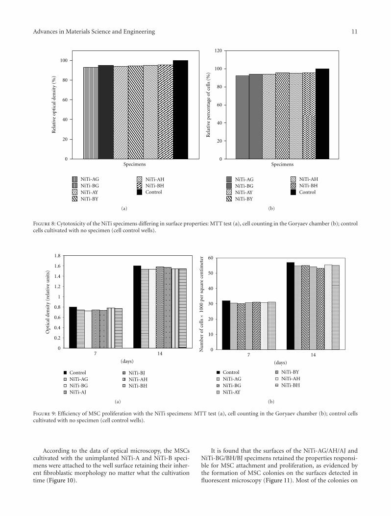
Advances in Materials Science and Engineering 11
0
20
40
60
80
100
Specimens
Rel
ativ
e op
tica
l den
sity
(%
)
NiTi-AGNiTi-BGNiTi-AYNiTi-BY
NiTi-AHNiTi-BHControl
(a)
0
20
40
60
80
100
120
Specimens
Rel
ativ
e pe
rcen
tage
of
cells
(%
)
NiTi-AGNiTi-BGNiTi-AYNiTi-BY
NiTi-AHNiTi-BHControl
(b)
Figure 8: Cytotoxicity of the NiTi specimens differing in surface properties: MTT test (a), cell counting in the Goryaev chamber (b); controlcells cultivated with no specimen (cell control wells).
0
0.2
0.4
0.6
0.8
1
1.2
1.4
1.6
1.8
7 14
(days)
ControlNiTi-AGNiTi-BGNiTi-AJ
NiTi-BJNiTi-AHNiTi-BH
Opt
ical
den
sity
(re
lati
ve u
nit
s)
(a)
0
10
20
30
40
50
60
7 14
(days)
ControlNiTi-AGNiTi-BGNiTi-AY
NiTi-BYNiTi-AHNiTi-BH
Nu
mbe
r of
cel
ls×
1000
per
squ
are
cen
tim
eter
(b)
Figure 9: Efficiency of MSC proliferation with the NiTi specimens: MTT test (a), cell counting in the Goryaev chamber (b); control cellscultivated with no specimen (cell control wells).
According to the data of optical microscopy, the MSCscultivated with the unimplanted NiTi-A and NiTi-B speci-mens were attached to the well surface retaining their inher-ent fibroblastic morphology no matter what the cultivationtime (Figure 10).
It is found that the surfaces of the NiTi-AG/AH/AJ andNiTi-BG/BH/BJ specimens retained the properties responsi-ble for MSC attachment and proliferation, as evidenced bythe formation of MSC colonies on the surfaces detected influorescent microscopy (Figure 11). Most of the colonies on

12 Advances in Materials Science and Engineering
(c) (1a) (1b)
(2a) (2b)
Figure 10: Morofology of MSCs calctivated with the NiTi-A and NiTi-B specimens: cultivation with no specimen (c), cultivation for 3 dayswith NiTi-A (1a) and NiTi-B (1b); cultivation for 14 days with NiTi-A (2a) and NiTi-B (2b). Optical microscope, magnification is ×50 for(c), (1a), (1b) and ×100 for (2a), (2b).
(a)
(b)
TN1-AG TN1-AJ TN1-AH
TN1-BG TN1-BJ TN1-BH
Figure 11: Images of fixed MSCs (prevailing colonies) stained with 6-carboxyfluorecein diacetate (6-CFDA) and DAPI on the NiTi specimensurfaces differing in chemical composition and roughness; 14th day of cultivation; magnification is ×10; cells are green, nuclei are blue.
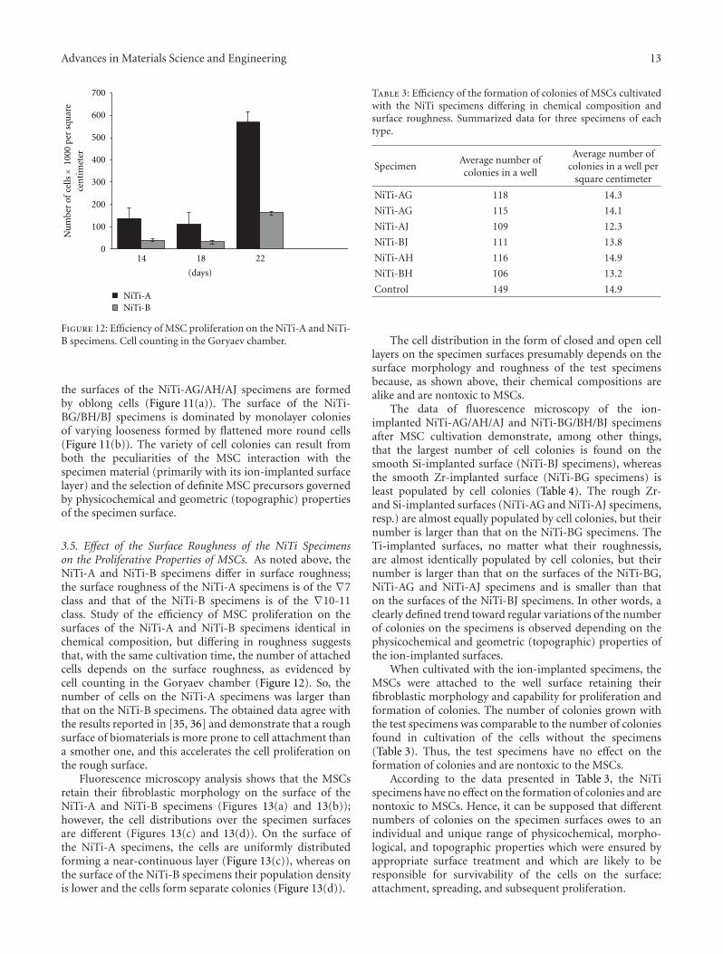
Advances in Materials Science and Engineering 13
0
100
200
300
400
500
600
700
14 18 22
(days)
NiTi-ANiTi-B
Nu
mbe
r of
cel
ls×
1000
per
squ
are
cen
tim
eter
Figure 12: Efficiency of MSC proliferation on the NiTi-A and NiTi-B specimens. Cell counting in the Goryaev chamber.
the surfaces of the NiTi-AG/AH/AJ specimens are formedby oblong cells (Figure 11(a)). The surface of the NiTi-BG/BH/BJ specimens is dominated by monolayer coloniesof varying looseness formed by flattened more round cells(Figure 11(b)). The variety of cell colonies can result fromboth the peculiarities of the MSC interaction with thespecimen material (primarily with its ion-implanted surfacelayer) and the selection of definite MSC precursors governedby physicochemical and geometric (topographic) propertiesof the specimen surface.
3.5. Effect of the Surface Roughness of the NiTi Specimenson the Proliferative Properties of MSCs. As noted above, theNiTi-A and NiTi-B specimens differ in surface roughness;the surface roughness of the NiTi-A specimens is of the ∇7class and that of the NiTi-B specimens is of the ∇10-11class. Study of the efficiency of MSC proliferation on thesurfaces of the NiTi-A and NiTi-B specimens identical inchemical composition, but differing in roughness suggeststhat, with the same cultivation time, the number of attachedcells depends on the surface roughness, as evidenced bycell counting in the Goryaev chamber (Figure 12). So, thenumber of cells on the NiTi-A specimens was larger thanthat on the NiTi-B specimens. The obtained data agree withthe results reported in [35, 36] and demonstrate that a roughsurface of biomaterials is more prone to cell attachment thana smother one, and this accelerates the cell proliferation onthe rough surface.
Fluorescence microscopy analysis shows that the MSCsretain their fibroblastic morphology on the surface of theNiTi-A and NiTi-B specimens (Figures 13(a) and 13(b));however, the cell distributions over the specimen surfacesare different (Figures 13(c) and 13(d)). On the surface ofthe NiTi-A specimens, the cells are uniformly distributedforming a near-continuous layer (Figure 13(c)), whereas onthe surface of the NiTi-B specimens their population densityis lower and the cells form separate colonies (Figure 13(d)).
Table 3: Efficiency of the formation of colonies of MSCs cultivatedwith the NiTi specimens differing in chemical composition andsurface roughness. Summarized data for three specimens of eachtype.
SpecimenAverage number ofcolonies in a well
Average number ofcolonies in a well per
square centimeter
NiTi-AG 118 14.3
NiTi-AG 115 14.1
NiTi-AJ 109 12.3
NiTi-BJ 111 13.8
NiTi-AH 116 14.9
NiTi-BH 106 13.2
Control 149 14.9
The cell distribution in the form of closed and open celllayers on the specimen surfaces presumably depends on thesurface morphology and roughness of the test specimensbecause, as shown above, their chemical compositions arealike and are nontoxic to MSCs.
The data of fluorescence microscopy of the ion-implanted NiTi-AG/AH/AJ and NiTi-BG/BH/BJ specimensafter MSC cultivation demonstrate, among other things,that the largest number of cell colonies is found on thesmooth Si-implanted surface (NiTi-BJ specimens), whereasthe smooth Zr-implanted surface (NiTi-BG specimens) isleast populated by cell colonies (Table 4). The rough Zr-and Si-implanted surfaces (NiTi-AG and NiTi-AJ specimens,resp.) are almost equally populated by cell colonies, but theirnumber is larger than that on the NiTi-BG specimens. TheTi-implanted surfaces, no matter what their roughnessis,are almost identically populated by cell colonies, but theirnumber is larger than that on the surfaces of the NiTi-BG,NiTi-AG and NiTi-AJ specimens and is smaller than thaton the surfaces of the NiTi-BJ specimens. In other words, aclearly defined trend toward regular variations of the numberof colonies on the specimens is observed depending on thephysicochemical and geometric (topographic) properties ofthe ion-implanted surfaces.
When cultivated with the ion-implanted specimens, theMSCs were attached to the well surface retaining theirfibroblastic morphology and capability for proliferation andformation of colonies. The number of colonies grown withthe test specimens was comparable to the number of coloniesfound in cultivation of the cells without the specimens(Table 3). Thus, the test specimens have no effect on theformation of colonies and are nontoxic to the MSCs.
According to the data presented in Table 3, the NiTispecimens have no effect on the formation of colonies and arenontoxic to MSCs. Hence, it can be supposed that differentnumbers of colonies on the specimen surfaces owes to anindividual and unique range of physicochemical, morpho-logical, and topographic properties which were ensured byappropriate surface treatment and which are likely to beresponsible for survivability of the cells on the surface:attachment, spreading, and subsequent proliferation.

14 Advances in Materials Science and Engineering
NiTi-A
NiTi-A
NiTi-B
NiTi-B
50μm 50μm
150μm 150μm
(a) (c)
(d)(b)
Figure 13: Fluorescence microscopy of MSCs transfected with a eGFP-N1 plasmid DNA on the NiTi-A and NiTi-B surfaces. Nuclei arestained with DAPI; 77th day of cultivation; magnification is ×20 (a), (b) and ×10 (c), (d).
Table 4: Efficiency of the formation of colonies of MSCs cultivated on the surface of the NiTi specimens differing in chemical compositionsand roughness. Summarized data for three specimens of each type.
Specimen Number of colonies Number of colonies on the specimen persquare centimeter
average for a specimen small medium-sized large merged
NiTi-AG 13 6 1 1 5 3.9
NiTi-BG 9 4 3 2 — 1.6
NiTi-AJ 20 7 7 4 2 3.75
NiTi-BJ 38 17 15 2 4 7.35
NiTi-AH 33 13 14 3 3 4.98
NiTi-BH 27 2 16 8 1 5.27
The developed surface roughness of a specimen increasesthe cell adhesion to the specimen surface [37], becausethe amount of extracellular matrix adhesion proteins on arough surface is much larger than that on a smooth one[38]. During the cultivation under the same conditions, theinitially rough surface of the NiTi-A specimens presumablyadsorbs more protein molecules from the culture medium toinvolve them in the cell adhesion than the initially smoothsurface of the NiTi-B specimens does. At the same time,
the degree of adhesion protein adsorption from a serum-containing culture medium is higher for rough surfacesthan for smooth ones [39]. It is conceivable that the levelof surface roughness of the NiTi-A and NiTi-AG/AH/AJspecimens with ion-implanted surface layers makes possiblean extracellular matrix necessary for cell adhesion with moreregular spatial organization compared to that formed onthe surface of the NiTi-B and NiTi-BG/BH/BJ specimenswith ion-implanted surface layers. As shown in [39], the

Advances in Materials Science and Engineering 15
best adhesion and proliferation of cells is furnished byfibronectin molecules whose spatial interrelation owes toroughness due to particles of size ∼200 nm rather thanby fibronectin molecules discretely adsorbed on a smoothsurface or surfaces of roughness due to particles of differentsize.
4. Conclusion
Thus, the research results allow the following conclusions.
(1) The chemical and physical parameters of the surfacesof all examined specimens suggest that before ionbeam treatment the specimens of two NiTi-A andNiTi-B series are alike in chemical composition andare different only in morphology and roughnesslevel. The ion beam treatment changes not only thechemical composition on the specimen surfaces, butalso the surface morphology such that the roughnessof the smoothest surfaces increases greatly and that ofthe rougher surfaces, on contrary, decreases.
(2) The experiments demonstrate that neither the unim-planted NiTi-A and NiTi-B specimens, nor theion-implanted NiTi-AG/AH/AJ and NiTi-BG/BH/BJspecimens reveal cytotoxic action on rat MSCs.Moreover, it is shown that the chemical compositionof the NiTi specimen surfaces before and after ionimplantation does not produce any damaging actionon MSCs. At the same time, the experiments suggestthat the NiTi-A and NiTi-B specimens fail to stim-ulate the proliferation of MSCs and this allows theassumption of bioinertness of their surface layers. Oncontrary, the NiTi-AG/AH/AJ and NiTi-BG/BH/BJspecimens with ion-implanted surface layers revealproperties favorable for proliferation of MSCs ontheir surfaces. Detailed studies of these specimens areexpected in the near future.
Acknowledgments
The work was performed under projects of SB RAS no.III.20.3.1 and 57 and was supported by state Contract of theMinistry of Education and Science of the Russian Federationno. 16.740.11.0140.
References
[1] S. A. Abugov, M. V. Puretsky, P. A. Rudenko et al., “Endovas-cular stenting of bifurcation stenosis in patients with ischemicheart disease,” Kardiologia, no. 8, pp. 7–11, 1998 (Russian).
[2] A. V. Sidelnikov, “Comparative evaluation of long-term effectsof coronary artery stenting with a Crossflex wire stent andtransluminal balloon angioplasty in IHD patients” (Russian),Candidate dissertation in medicine, Moscow, Russia, p. 20,2002.
[3] I. I. Kornilov, O. K. Belousov, and E. V. Kachur, TitaniumNickelide and Other Shape Memory Alloys, Nauka, Moscow,Russia, 1977.
[4] A. I. Lotkov, V. N. Khachin, V. N. Grishkov, L.L. Meisner,and V. P. Sivokha, “Shape memory alloys,” in Physical
Mesomechanics and Computer-Aided Design of Materials, vol.2, pp. 202–213, Nauka, Novosibirsk, Russia, 1995.
[5] V. N. Zhuravlev and V. G. Pushin, Thermomechanical ShapeMemory Alloys and Their Application in Medicine, UrB RAS,Ekaterinburg, Russia, 2000.
[6] L. L. Meisner, “Mechanical and physicochemical properties ofNiTi-based alloys with thin surface layers modified by chargedparticle flows,” Physical Mesomechanics, vol. 7, part 2, pp. 169–172, 2004.
[7] A. I. Lotkov, L. L. Meisner, and V. N. Grishkov, “NiTi-basedalloys: ion-beam, plasma, and chemical surface modification,”Fizika Metallov i Metallovedenie, vol. 99, no. 2, pp. 1–13, 2005(Russian).
[8] D. Williams, Biocompatibility of Clinical Implant Materials,CRC Press, Boca Raton, Fla, USA, 1981.
[9] S. A. Shabalovskaya, J. Anderegg, F. Laab, P. A. Thiel, and G.Rondelli, “Surface conditions of NiTinol wires, tubing, andas-cast alloys. The effect of chemical etching, aging in boilingwater, and heat treatment,” Journal of Biomedical MaterialsResearch: Part B, vol. 65, no. 1, pp. 193–203, 2003.
[10] V. I. Sevostianov, Ed., Biocompatibility, 1999.[11] V. P. Shakhov, I. A. Khlusov, G. S. Dambaev et al., “Meth-
ods of analysis of cellular cultures, artificial organs, andbiomaterials,” in Introduction into Methods for Cell Culture,Bioengineering of Organs and Tissues, pp. 340–349, STT,Tomsk, Russia, 2004.
[12] N. A. Korzh, L. A. Kladchenko, and S. V. Malyshkina,“Implant materials and osteogenesis. Role of optimization andstimulation in bone repair,” Orthop. Traum. Protez., no. 4, pp.5–14, 2008 (Russian).
[13] E. V. Vladimirskaya, O. A. Maiorova, S. A. Rumyantsev, and A.G. Rumyantsev, “Stem cells and intercellular interactions,” inBiological Basis and Prospects of Stem Cell Therapy, pp. 74–102,Medpraktica-M, Moscow, Russia, 2005.
[14] S. A. Kuznetsov, A. J. Friedenstein, and P. G. Robey, “Factorsrequired for bone marrow stromal fibroblast colony formationin vitro,” The British Journal of Haematology, vol. 97, no. 3, pp.561–570, 1997.
[15] D. C. Miller, K. M. Haberstroh, and T. J. Webster, “PLGAnanometer surface features manipulate fibronectin interactionfor improved vascular cell adhesion,” Journal of BiomedicalMaterials Research: A, vol. 81, pp. 678–684, 2006.
[16] S. M. Chesnokov, “Wide-aperture ion source,” RF patentnumber RU 1598757, registered in the State Register 16.11.93.
[17] V. P. Sergeev, V. P. Yanovsky, and Yu. N. Paraev, “Extended ionsource,” RF patent number RU 2261497, Bulletin of inventionsnumber 27, 2005.
[18] A. I. Lotkov, S. G. Psakhie, and V. P. Sergeev, “Formationof nonequilibrium states in surface layers of materials byelectron-ion plasma technologies,” in Surface Nanoengineer-ing, N. Z. Lyakhov and S. G. Psakhie, Eds., pp. 227–275,Publishing house of SB RAS, Novosibirsk, Russia, 2008.
[19] D. I. Potter, M. Ahmed, and S. Lamond, “Microstructuraldevelopments during implantation of metals,” in Proceedingsof the Ion Implantation and Ion Beam Processing of Materials,vol. 27 of Materials Research Society Symposia Proceedings, pp.117–126, 1984.
[20] J. K. Hirvonen, Ed., Ion Implantation into Metals, Metallurgia,Moscow, Russia, translation from English edited by O. P.Elyutin, 1985.
[21] L. Clapham, “High dose, heavy ion implantation into metals:the use of sacrificial surface layers to enhance retention,”Surface and Coatings Technology, vol. 65, no. 1–3, pp. 24–29,1994.

16 Advances in Materials Science and Engineering
[22] M. Nastasi, J. W. Mayer, and J. K. Hirvonen, Ion-SolidInteractions: Fundamentals and Applications, vol. XXVII ofCambridge Solid State Science Series, Cambridge UniversityPress, Cambridge, UK, 1996.
[23] T. Mosmann, “Rapid colorimetric assay for cellular growthand survival: application to proliferation and cytotoxicityassays,” Journal of Immunological Methods, vol. 65, no. 1-2, pp.55–63, 1983.
[24] T. Yu. Tatarenko-Kozmina, Pathophysiological mechanisms ofapplication of mesenchymal stem cells on synthetic composites foroptimization of bone tissue regeneration, Doctoral dissertationin biology, Moscow, Russia, 2007.
[25] N. A. Plokhinsky, Biometry, MSU Publishing House, Moscow,Russia, 1970.
[26] A. G. Akimov, “On the mechanisms of the formation of pro-tective oxide layers in “metal (alloy)—medium“ systems,”Zashchita Metallov, vol. XXII, no. 6, pp. 879–886, 1986(Russian).
[27] L. L. Meisner, V. P. Sivokha, A. I. Lotkov, and E. G. Barmina,“Corrosion resistance of quasibinary NiTi–TiAu alloys inbiochemical solutions,” Fiz. Khim. Obr. Mater., no. 1, pp. 78–84, 2006 (Russian).
[28] S. A. Shabalovskaya, H. Tian, J. W. Anderegg, D. U. Schryvers,W. U. Carroll, and J. V. Humbeeck, “The influence of surfaceoxides on the distribution and release of nickel from Nitinolwires,” Biomaterials, vol. 30, no. 4, pp. 468–477, 2009.
[29] L. L. Meisner, V. P. Sivokha, A. I. Lotkov, and L. A.Derevyagina, “Surface morphology and plastic deformation ofthe ion-implanted TiNi alloy,” Physica: B, vol. 307, no. 1–4, pp.251–257, 2001.
[30] L. L. Meisner, V. P. Sivokha, A. I. Lotkov, and E. G. Barmina,“Effect of ion implantation on shape memory characteristicsof TiNi alloy,” Journal de Physique IV, vol. 112, pp. 663–666, 2003, Proceedings of the International Conference onMartensitic Transormations, (ICOMAT ’020), Espoo, Finland,June, 2002.
[31] L. Tan, R. A. Dodd, and W. C. Crone, “Corrosion and wear-corrosion behavior of NiTi modified by plasma source ionimplantation,” Biomaterials, vol. 24, no. 22, pp. 3931–3939,2003.
[32] A. I. Lotkov and A. A. Baturin, “Vacancy defects in metals,alloys, and intermetallic compounds with martensite transfor-mations,” Materialovedenie, no. 7, pp. 39–44, 2000.
[33] F. V. Nolfi, Ed., Phase Transformations during Irradiation,Metallurgia, Chelyabinsk, Russia, Translated from English byM. E. Reznitsky, V. M. Ustintschikov, and A. B. Tsepelev,Edited by L.N. Bystrov, 1989.
[34] B. D. Ratner and A. S. Hoffman, “Physicochemical surfacemodification of materials used in medicine,” in BiomaterialsScience: An Introduction to Materials in Medicine, B. D. Ratner,Ed., pp. 201–218, Elsevier, 2nd edition, 2004.
[35] K. Anselme, “Osteoblast adhesion on biomaterials,” Biomate-rials, vol. 21, no. 7, pp. 667–681, 2000.
[36] E. Eisenbarth, P. Linez, V. Biehl et al., “Cell orientationand cytoskeletion organization on ground titanium surfaces,”Biomolecular Engineering, no. 19, pp. 233–237, 2002.
[37] R. A. Pareta, A. B. Reising, T. Miller, D. Storey, and T. J.Webster, “An understanding of enhanced osteoblast adhesionon various nanostructured polymeric and metallic materialsprepared by ionic plasma deposition,” Journal of BiomedicalMaterials Research: Part A, vol. 92, no. 3, pp. 1190–1201, 2010.
[38] J. Marleta, J. Uptonac, R. Langerbo, and J. P. Vacantica,“Transplantation of cells in matrices for tissue regeneration,”Advanced Drug Delivery Reviews, no. 3, pp. 165–182, 1998.
[39] D. C. Miller, K. M. Haberstroh, and T. J. Webster, “Mech-anism(s) of increased vascular cell adhesion on nanostruc-tured poly(lactic-co-glycolic acid) films,” Journal of BiomedicalMaterials Research: Part A, vol. 73, no. 4, pp. 476–484, 2005.

Hindawi Publishing CorporationAdvances in Materials Science and EngineeringVolume 2012, Article ID 902649, 13 pagesdoi:10.1155/2012/902649
Review Article
Tunnel Contacts for Spin Injection into Silicon: The Si-CoInterface with and without a MgO Tunnel Barrier—A Study byHigh-Resolution Rutherford Backscattering
S. P. Dash,1, 2 D. Goll,2, 3 P. Kopold,2 and H. D. Carstanjen2
1 Department of Microtechnology and Nanoscience, Chalmers University of Technology, 412 96 Goteborg, Sweden2 Max Planck Institute for Intelligent Systems (Formerly Max Planck Institute for Metals Research), Heisenbergstrβe. 3,70569 Stuttgart, Germany
3 Materials Research Institute, Aalen University, Beethovenstraβe. 1, 73430 Aalen, Germany
Correspondence should be addressed to S. P. Dash, [email protected]
Received 30 June 2011; Revised 20 September 2011; Accepted 20 September 2011
Academic Editor: Adam Georg Balogh
Copyright © 2012 S. P. Dash et al. This is an open access article distributed under the Creative Commons Attribution License,which permits unrestricted use, distribution, and reproduction in any medium, provided the original work is properly cited.
In order to obtain high spin injection efficiency, a ferromagnet-semiconducor Schottky contact must be of high crystalline quality.This is particularly important in the case of ferromagnet-silicon interfaces, since these elements tend to mix and form silicides.In this study Co-Si (100) interfaces were prepared in three different ways: by evaporation at room temperature, low temperature(−60◦C), and with Sb as surfactant, and their interface structures were analyzed by high-resolution RBS (HRBS). In all cases moreor less strong in-diffusion of Co with subsequent silicide formation was observed. In order to prevent the mixing of Co and Si,ultra thin MgO tunnel barriers were introduced in-between them. In situ HRBS characterization confirms that the MgO filmswere very uniform and prevented the mixing of the Si substrate with deposited Co and Fe films effectively, even at 450◦C.
1. Introduction
Exploiting the spin of the electron in addition to its chargeto explore a new generation of spintronic devices whichwill be smaller, more versatile and more robust than thosecurrently making up silicon chips have both fundamentaland technological importance [1–7]. High spin polarizationof Co at room temperature (∼40%) [8] and expected longspin coherence length in Si (longer than micrometers) [9]make the material couple Co and Si attractive for spininjection experiments. In such a heterostructure of a Co thinfilm on a Si substrate, any structural disorder at the interfacewould drastically reduce the spin polarization at the interfaceand, hence, the spin injection efficiency [10–15]. If a smallamount of Co diffuses into the Si, each such Co atom will belikely to carry a local magnetic moment oriented randomlywith respect to the magnetization direction of the Co thinfilm. They will scatter the injected spin polarized electrons,thereby degrading their spin polarization [14, 15].
Co and Si are known to form various types of silicidesthat exhibit different degrees of magnetization, that is,
nonmagnetic, paramagnetic, or ferromagnetic. When spin-polarized electrons pass through such a silicide region,their polarization is very likely to degrade. The processesinvolved have not been treated completely and in detail upto present, but the following effects may play an importantrole: electrons enter a region of different magnetization(magnitude or orientation). Electrons pass a rough interfacebetween regions of different magnetization; such roughinterfaces are known to cause strong depolarization [10].In paramagnetic areas the magnetic moments commonlyare not oriented; similarly to the above case of isolated Coatoms they will scatter the injected electrons. In a similarway any kind of magnetic defect may work. One also shouldnot forget about the depolarizing influence of the variousSchottky contacts between different silicides.
Thus in order to control and improve the propertiesof the interface, a detailed understanding of its structure isnecessary. In this paper we present results where we studiedthe Co-Si (100) interface prepared in four different ways: (1)by deposition of Co at room temperature, (2) by depositionof Co at low temperature (−60◦C), (3) by deposition of Co

2 Advances in Materials Science and Engineering
at room temperature using Sb as surfactant, and (4) witha MgO tunnel barrier at the Co-Si interface. The differenttypes of interfaces were analyzed in situ, that is, duringpreparation by high depth resolution Rutherford backscat-tering spectroscopy (HRBS). The HRBS data in turn providedepth profiles of Co, Si, Sb, Mg, and O with monolayerdepth resolution. In this way they give information about thesharpness of the interface and the homogeneity of the Co andMgO thin films and allow in particular identifying varioustypes of cobalt silicides as a function of depth. The data onthe Co-Si Schottky interface have been published before inthree publications [16–18] and are here summarized in acomparative way. The data on the MgO tunnel barrier arenew.
2. The Direct Co-Si (100) (Schottky) Interface
2.1. Introduction. The phenomena observed at the initialstages of Co deposition on a Si substrate seem to be uniqueand depend on the preparation conditions and are stilldiscussed controversially [19–23]. About the growth mode ofCo on Si, Cho et al. [19] suggested that the Co atoms growin a layer-by-layer mode, without any interdiffusion, whereasMeyerheim et al. [20] and Rangelov et al. [21] could see anin-diffusion of Co atoms for coverages higher than 0.5 MLof Co. For the Si (100) surface, AES and surface-extended X-ray-absorption fine-structure (EXAFS) measurements [19–23] showed that one can distinguish between several stagesof the initial adsorption of Co on Si (100) surfaces at roomtemperature. About the atomic positions of Co atoms onSi (100) (see Figure 1), Meyerheim et al. [20], Scheuchet al. [22], and Gomoyunova et al. [23] found that Co isadsorbed in fourfold hollow sites (nearly in plane, d ≈ 0)in every second (110) row of the Si (100) surface. Choet al. [19] have found that the preferred adsorption sitesare on top of a Si dimer (T4 sites) and sites spanningthe (110) trench (HB sites). However, density functionalcalculations [24] suggested that the T4 and HB sites areenergetically unfavourable (see Figure 1). Concerning thepositions of the in-diffused Co atoms, Meyerheim et al. [20]could distinguish between several stages of growth. In theregime of 0.5–2.5 ML, Co atoms diffuse into the Si latticeoccupying interstitial sites, for the regime above 2.5 ML thesubstitution of the Si host atoms by Co takes place, and forcoverages above 19 ML a locally ordered metallic overlayerstarts to grow.
Controversies also exist about the growth mode of Co.Does there exist a critical coverage of Co for the in-diffusionof Co and the out-diffusion of Si atoms? How thick is thesilicide layer formed at the interface, what is its chemicalcomposition, and which are the diffusing species at differentstages of growth?
In a previous letter [16] we have addressed some of thesecontroversies by an in situ investigation of the growth of thinCo films (0.08–2.93 ML) on Si (100) at room temperaturewith high-resolution Rutherford backscattering spectrome-try (HRBS). It turned out that Co diffuses into the Si bulkright from the beginning, that is, already at a Co coverage aslow as 0.08 ML. For higher coverage various silicide phases
start to grow at the surface, but no pure Co film, even atthe highest coverage (2.93 ML of Co) is investigated in thisstudy. In order to reduce the in-diffusion of Co and the out-diffusion of Si and to enhance the growth of layers of pure Cotwo ways were followed in two subsequent investigations: (a)Co deposition was done while keeping the substrate at lowertemperature, –60◦C [17]; (b) a thin layer of surfactant (1 MLof Sb) was used to reduce the amount of out-diffusion of Sito the surface during Co deposition [18]. Both techniqueswere helpful to reduce the silicide formation to some extentbut could not stop it in total. The results of these threeinvestigations are reported in a summarized version in thesubsequent Sections 2.2 and 2.3.
2.2. Experimental. The in situ HRBS measurements wereperformed in an ultra high vacuum (UHV) system con-sisting of a preparation chamber, connected to a Pelletronaccelerator, and an electrostatic spectrometer [25] for energyanalysis of the scattered ions. In case of room temperature(RT) and low-temperature (LT) deposition of Co, 2 MeV N+
ions at incidence angles of 2◦ to the sample surface andat a scattering angle of 37.5◦ were used for the HRBSanalysis. The energy resolution of the spectrometer setupwas 4 keV in this case which corresponds to 1 A depthresolution in Si and 0.5 A in Co. In two cases (surfactant-mediated deposition and RT deposition of higher amountsof Co, Figure 4) 2 MeV He+ ions were used for analysiswith incidence angles of 7.5◦ and 4.5◦, respectively, but thesame scattering angle of 37.5◦. According to this scatteringangle all analysis experiments presented here are actually“forward scattering experiments”, but from principle forwardand backscattering are all Rutherford scattering. And sinceRutherford backscattering spectroscopy (RBS) is the farbetter known technique, we will call it HRBS in the following.We also want to note that, in order to minimize effects ofradiation damage due to the ion beam, a new beam spot onthe Si wafer was used for each measurement. Control spectrawas taken on the same spot to estimate the influence ofradiation damage and potential mixing, but within statisticalerrors no effect was found.
For the deposition experiments chemically cleaned n-Si (100) with resistivity of 4–10Ω cm (P doped) were usedwhich were further cleaned in UHV by flash heating at950◦C. From this temperature the samples were slowlycooled down to RT or −60◦C, depending on the experimen-tal requirement. These temperatures were maintained as wellduring Co deposition as during the HRBS measurements.The surface cleanness of the Si samples was verified by HRBSmeasurements (sensitivity about 5%). Co with 4 N puritywas evaporated from an effusion cell at a rate of 0.05 ML/min(1 ML = 6.87 × 10¹⁴ atoms/cm2 = number density of Si(100) layers). Before use the effusion cell was outgassed; noC or O contaminants were found during evaporation. Theevaporation rate was calibrated by HRBS with an accuracyof about 5%. As mentioned above, each HRBS spectrumwas taken on a new spot (size ∼1 mm2) to minimize theinfluence of radiation damage. In the case of surfactant-mediated growth of Co, 1 ML of Sb was deposited before theevaporation of Co. This monolayer of Sb was supposed to

Advances in Materials Science and Engineering 3
First-layer Si
Second-layer Si
Third-layer Si
Forth-layer Si
[110]
[110]
HH
HB
B2 T3
T4
Figure 1: The initial Co adsorption sites T4, HB, HH, and T3 on the Si (100)-(2 × 1) surface at room temperature. B2 is the “cave site” forMg mentioned in Section 3.3.
float at the surface of the deposited Co, in this way preventingthe outdiffusion of Si.
2.3. Results and Discussion. Figures 2(a) and 2(c) showHRBS spectra of Co on Si (100) during the deposition ofsmall amounts of Co (less than 3 ML) for the substratetemperatures of 20◦C and −60◦C, respectively. In addition,Co depth profiles are shown in Figures 2(b) and 2(d) asobtained from the spectra by simulating the spectra withthe computer code RUMP [26]. In these simulations the Sisample was subdivided into monolayers of Si (each 6.87 ×10¹⁴ atoms/cm2 thick) and the Co concentration in each layeradjusted until an optimum fit between simulation and HRBSspectrum was obtained. As is obvious from the spectra, Coatoms diffuse into the Si sample right from the beginning ofthe deposition at both deposition temperatures—as expectedto larger depths for the higher temperature. As seen further,an enrichment of Co is present in the top-most layers whichis the first Si layer at 20◦C (layer 0 in Figure 2(b)) and the firstadsorption layer at −60◦C (layer +1 in Figure 2(d)). Besides,the deposition at RT leads to the development of a subsurfaceenrichment of Co (about 2-3 Si layers below the surface, seeFigure 2(a)). This is similar to results about a subsurface Au-enriched phase in a liquid AuSi alloy [27]. In these systemssuch a configuration is stabilized by the minimization ofthe free energy, essentially consisting of atomic binding andsurface energies, and the entropy of mixing. In solids strainenergy enters in addition. At low temperature, a differentdepth profile is observed. It consists of a diffusion profile,
overlaid by oscillations (Figure 2(c)). The oscillations are dueto the fact that every second Si layer is Co depleted. This issimilar to the model for the diffusion microstructure of Niin Si (100) by Chang and Erskine [28] and the distributionof metal atoms in metal alloys like Cu3Au [29] close tothe surface. A similar behaviour is also observed for thegrowth of Fe on Si (100) at very low coverage at roomtemperature [30]. Again such a configuration is stabilizedby the minimization of the Gibbs-free energy, consisting ofatomic binding, strain and surface energies, and the entropyof mixing.
With increasing amounts of deposited Co (see Figures 3and 4), first various types of partially also stoichiometricsilicides appear at the surface until, finally, layers of pure Cogrow on top of them. However, great differences are observedas well in the onset of the growth of pure Co layers as in thecomposition and distribution of the silicides. They seem todepend strongly on the growth conditions, that is, growthat RT, LT, or with Sb as surfactant. While for Co depositionat RT the formation of such a pure layer of Co is first seenat an amount of about 23 ML of deposited Co (Figure 3),it is already observed for amounts of about 6 ML of Cofor LT (Figure 3) and 3 ML of Co for surfactant-mediateddeposition (Figure 4). Concerning silicide formation, atRT deposition almost stoichiometric CoSi (below 6 ML:Co0.6Si0.4, above 6 ML: Co0.5Si0.5) forms at the interfacewhich grows thicker and thicker (Figures!3 and 4). Only athigh amounts of deposition also other phases form as kindof transition between Si bulk and CoSi, and CoSi and Co at

4 Advances in Materials Science and Engineering
1770 1780 1790 1800 1810 18200
20
40
60
801.19 ML
0.08 ML
0.22 ML
0.3 ML
0.5 ML
0.93 ML
Cou
nts
Energy (keV)
0.5 nm
Co
− 7 − 5 − 3 − 1 10
0.050.1
0.08 ML
Monolayer
00.10.2 0.22 ML
00.10.2
0.30 ML
00.10.2 0.50 ML
00.10.2
0
0.4 1.19 ML
0.93 ML
Si surfaceBulk Si layers
Co/
Si
Room temperature growth
(a) (b)
0.1 ML
0.36 ML
0.72 ML
1.08 ML
1.3 ML
1770 1780 1790 1800 18100
10
20
30
Energy (keV)
Cou
nts
0.5 nm
Co
Co/
Si
Si surfaceCo on top
Si bulk
− 4 − 3 − 2 − 1 0 10
0.050.1
0
0.2
0
0.2
0
0.2
0
0.2
Monolayers
1.3 ML
1.08 ML
0.72 ML
0.36 ML
0.1 ML
Low temperature growth
(c) (d)
Figure 2: Co on Si (100), low coverage (≤1.3 ML). Panels at the left-hand side: Co edge of HRBS spectra (circles) and RUMP simulations(solid lines). Panels at the right hand side: Co concentrations as determined by the RUMP simulations versus depth (depth scale: monolayersof Si, each 6.87 · 1014 at./cm2 thick). (a) Co deposition at RT. The peaks between 1800 and 1810 keV are due to backscattering from Co atthe surface, the other peaks in the range of 1785–1800 keV due to Co atoms in the Si bulk (subsurface enrichment). (b) Co concentrationprofiles (Co/Si) in subsequent layers of the sample as obtained from (a) by RUMP simulations. Layer 0 is the topmost Si layer; −1, −2, −3,−4, and −5 are subsequent layers in the bulk. Note that the y-axes for 0.08 and 1.19 ML have scales different from others. (c) Co depositionat −60◦C. The peaks between 1800 and 1805 keV are due to backscattering from Co at the surface. The oscillations in the Co concentrationmentioned in the text are clearly visible. (d) Co concentration (Co/Si) in the various Si (100) layers of the Si crystal as derived from (c) byRUMP simulations. Layer 1 (hatched column) corresponds to Co atoms on top of the Si crystal, layer 0 is the first Si layer, and layers −1, −2,−3, and −4 are subsequent layers in the Si bulk (solid columns).
the surface: at the Si-CoSi interface a CoSi2-like phase andtowards the surface a Co2Si phase. This is different for LTand surfactant-mediated deposition. At LT deposition theCo0.5Si0.5 phase forms at the interface, followed by a low-concentration tail of Co towards the Si bulk (Figure 3). It issimilar to the case of surfactant-mediated deposition. Here
the “Co tail” consists of a layer of 10 ML of CoSi2 at theinterface and another 7 ML of CoSi4 towards the Si bulk(Figure 4). This interface structure stabilizes at 19 ML ofdeposited Co and stays like this up to the highest amountof Co deposited in this investigation, that is, 38 ML. It isinteresting to note that the surfactant Sb stays, as expected, at

Advances in Materials Science and Engineering 5
1550 1600 1650 1700 1750 18000
10
20
30
40
50
0 10 20 30
0
0.2
0.4
0.6
0.8
1CoSi
Monolayers
Con
cen
trat
ion
5.93 MLCo
Cou
nts
Energy (keV)
Si
Low temperature growth
(a)
1860 1880 1900 1920 1940
0
100
200
300
400
500
0 10 20 30 40 50
0
0.2
0.4
0.6
0.8
1Co
Con
cen
trat
ion
Monolayers
Si
Co
Si
Cou
nts
Energy (keV)
23.4 ML
Room temperature growth
(b)
Figure 3: HRBS spectra of both the Si and Co edges: (a) 5.93 ML of Co deposited at −60◦C and (b) 23.42 ML of Co deposited at roomtemperature (22◦C), together with simulations of the spectra by RUMP (solid lines through the data). The insets show the Si and Coconcentrations at the interface as obtained from the RUMP simulations (depth scale: monolayers of Si, each 6.87 · 1014 at./cm2 thick). Theright hand side of the concentration profiles corresponds to the free surface of the Co/Si. Layer 0 was deliberately put into the Si bulk.
the surface of the sample during deposition (see Figure 4(b)).Only at larger amounts of deposited Co some mixing of Sband Co occurs.
In Figure 5, finally, the Co and Si depth profiles for thethickest deposited layers of Co as obtained from the RUMPsimulations are compared for the three different depositionconditions. As already stated above, the structures of the Co-Si interfaces exhibit marked differences. for Co deposition atRT (23 ML, Figure 5(c)) a broad layer of Co0.5Si0.5 (18.8 A) isformed between two thin transition layers of CoSi2 (2.2 A)and Co2Si (3.75 A). Only a very thin layer of pure Co ispresent. For Co deposition at LT (5.93 ML, Figure 5(b)) alsoin this case thin layer of Co0.5Si0.5 exists at the interface witha thin layer of pure Co on top. (The thinness of this layer isdue to the small amount of deposited Co. It would certainlygrow for higher amounts of Co.) But here a long tail ofdifferent low-Co concentration silicides is observed towardsthe Si bulk. For surfactant-mediated deposition a similar tailof low-Co concentration silicides is found, but in this caseit consists, as said above, of two well-defined silicides withstoichiometric compositions: 10 ML of CoSi2 and 7 ML ofCoSi4. The Co0.5Si0.5 phase, present in the other cases, couldnot be found.
It should be noted that in all cases flat surfaces are main-tained during Co deposition. No roughening is observed;it should show up in rounding off of the high-energy edgeof the HRBS spectra [31] which is absent in all cases. Athigher amounts of deposited Co even a layer-by-layer growthoccurs. This is perhaps most evident from the HRBS spectraof Sb-mediated growth at RT from Figure 4(b). Here the
high-energy Si edge shifts almost parallel with increasing Codeposition, since a homogeneous Co film builds up on top.No Si is found at the surface; only the Co film is gettingthicker. This is a clear indication of Sb working as surfactantproperly: due to its low surface energy Sb suppresses thesegregation of Si at the surface and apparently also theformation of additional silicides at the interface. This isdifferent for RT deposition of Co without Sb as surfactant.Here right from the beginning a CoSi-like phase is formedcontinuously, until a large amount of deposited Co (about16 ML) first a Co2Si phase and finally (after about 23 ML ofCo) a film of pure Co starts to grow. But also here no Si issegregating at the surface in the form of a layer of pure Si.This would definitely be visible in the Si HRBS spectrum ofFigure 4(a). These observations contrast to a certain degreeto the findings of a very recent paper by Pronin et al. [32].There the authors studied RT deposition of Co on Si (100) byhigh-resolution photoelectron spectroscopy and a few othertechniques in a thorough investigation. The authors claimthe segregation of a Si surface layer and, besides, the growthof a layer of pure Co, starting at a Co coverage of about0.7 nm. Both findings seem not to be in agreement with ourobservations. It will be interesting to solve this riddle and finda solution which satisfies both investigations.
We finally want to note that there exist differences in thesurface energy of the Cobalt spectra presented in differentpanels. They are due to slightly different incident energiesof the ion beam, since the experiments were performed ondifferent days.

6 Advances in Materials Science and Engineering
1860 1880 1900 1920 19400
100
200
300
400
500
16 ML
Si clean Si
3.48 ML
Cou
nts
Energy (keV)
23.42 ML
11.8 ML
6 ML
2 ML
Co
0 10 20 30 40 500
0.51
3.48 ML
Monolayers
2 ML
00.5
1
5.4 ML
00.5
1
11.83 ML
00.5
1
17.65 ML
Con
cen
trat
ion
00.5
123.42 ML
00.5
1
SiCo
(a) (b)
Room temperature growth—no Sb mediated
1850 1875 1900 1925 19500
100
200
300
400
500
Sb
Co
Cou
nts
Energy (keV)
Si
38 ML Co
30 ML Co
19 ML Co
10 ML Co
3 ML Co
SiCo
0 10 20 30 40 50 600
0.5
1
10 ML
3 ML
Monolayers
0
0.5
1
0
0.5
1
38 ML
30 ML
19 ML
Con
cen
trat
ion 0
0.5
10
0.5
1
(c) (d)
Room temperature growth—Sb mediated
Figure 4: Co on Si, higher coverage (≥2 ML). Panels at left-hand side: Co and Si (and Sb) HRBS spectra (circles) and RUMP simulations(solid lines). Panels at the right-hand side: Co and Si concentrations as derived by RUMP (depth scale: monolayers of Si, each 6.87 ·1014 at./cm2 thick). The right-hand side of the concentration profiles corresponds to the free surface of the samples. (a) Co depositionat RT. (b) Co and Si concentration profiles derived from (a). (c) Surfactant-mediated deposition of Co at RT. (d) Co and Si concentrationprofiles derived from (c). The right-hand side of the concentration profiles corresponds to the free surface of the samples. The right-handside of the concentration profiles corresponds to the surface of the Co/Si samples (which in case of the Sb-mediated deposition is below anSb layer). Layer 0 was deliberately put into the Si bulk.
3. The Co-Si (100) Interface witha MgO Tunnel Barrier
3.1. Introduction. As evident, for example, from the resultspresented in Section 2, Co-Si (100) interfaces are in no way
sharp with an abrupt transition between Co and Si but showdiffusion of Co and Si with spontaneous silicide formationat the interface at room temperature [16, 20] and evenbelow room temperature [17]. This structural disorder atthe interface would drastically reduce the spin-polarization

Advances in Materials Science and Engineering 7
0 10 20 30 40
0
0.4
0.8
1.2
CoSi
Monolayers
Sb
Con
cen
trat
ion
Sb mediated growth
(a)
0 10 20 30 40Monolayers
0
0.4
0.8
1.2
Si
LT growth Co
Con
cen
trat
ion
(b)
0 10 20 30 40
Monolayers
Co
0
0.4
0.8
1.2RT growth
Con
cen
trat
ion Si
(c)
Figure 5: Co and Si (and Sb) concentrations as derived by RUMP simulations from the HRBS data of Figures 3 and 4. (c) Growth of 23.4 MLof Co on Si at room temperature, (b) 5.93 ML of Co deposited at low temperature (−60◦C), and (a) growth of 19 ML of Co on Si with Sb asa surfactant. They seem to be representative for the interface structure in a stationary state. The free surface of the three samples is located atthe right-most rim of the profiles. Layer 0 was deliberately put into the Si bulk.
at the interface and, hence, the spin injection efficiency [15].On the other hand, tunnel barriers in between a ferromagnetand a semiconductor have proven to be high-quality spin-selective barriers in a prototype GaAs system [33, 34] and,most recently, in the case of Si [1, 10–12, 35–37]. Using atunnel barrier on Si has mainly two advantages: (i) it formsa chemical barrier between the FM and the Si and (ii) ithas a good spin-selective tunnel resistance. When an Al2O3
tunnel contact is used [1, 10–12, 35, 36], the maximumspin injection that can be achieved might be limited bythe scattering and depolarization of spin-polarized carriersdue to its amorphous nature. An alternative approach forincreasing the spin polarization is to use a crystalline MgOtunnel barrier. There a large spin polarization (∼50%) wasachieved using a CoFe/MgO tunnel injector on a GaAs LEDstructure [34].
In the present study magnesium oxide (MgO) was chosenas tunnel barrier on Si for several reasons. (i) It is chemicallyinert and thermally stable and should, therefore, result insharp interfaces with both Si and ferromagnetic metals,(ii) MgO has a wide band gap (7.3 eV), ensuring a largeband offset with Si to minimize leakage currents, and (iii)the crystalline properties will facilitate coherent tunnellingof spin polarized electrons. MgO is a highly insulatingcrystalline solid with NaCl structure. The lattice constantof MgO is 4.211 A, whereas that of Si is 5.431 A, implying
a direct lattice mismatch of −22.5%, but there is a nearcommensurate match with Si at a 4 : 3 ratio of the latticeconstants (four MgO to three Si lattice constants). Fork etal. first reported epitaxial growth of thick MgO films on Si(100) by pulsed laser deposition [38]. The interface with Siwas found to be incommensurate but abrupt and free fromsecondary phases or interdiffusion. Also for the case of anultra-thin MgO film on Si (100), the interface is expectedto be incommensurate at the early stages of growth due tothe presence of large lattice mismatch. So the minimizationof the defect density in the epitaxial growth of an ultra-thinMgO film on Si (100) can be a real challenge.
For the realization of a high tunnelling magneto-resistiveeffect, the ultra-thin MgO barrier on Si should satisfy certainimportant issues. First, the tunnel barrier should be pin-hole free: the requirement for low-resistance tunnel junctionspushes the barrier thickness to lower length scales, makingbarrier pinholes a real and significant problem. The relativecontributions from the two conduction channels—elastictunneling through the insulating spacer and ballistic spinpolarized transport through the narrow pinhole shorts—canalso change the magnetoresistive response [39]. Secondly, thethermal stability of the ferromagnetic metals on thin tunneljunctions is important, due to compatibility issues withexisting complementary metal-oxide semiconductor CMOSprocesses, that is, for the production of magnetic random

8 Advances in Materials Science and Engineering
1300 1400 1500 16000
100
200
300
400 MgC
oun
ts
Energy (keV)
O
Si afterMgO
Si
(a)
Si
Co
MgO
(b)
Figure 6: (a) HRBS spectra of a Si sample before and after MgO evaporation. Before evaporation: spectrum of the high-energy Si edge(solid circles) and RUMP simulation (solid line) of the clean Si. After MgO evaporation: spectrum of Si with Mg and O peaks of the 18.3 MLthick MgO film on top (open circles) and RUMP simulation (solid line) of the 18.3 ML thick MgO film as prepared on Si (100) surface.The spectrum shows that the MgO film is very uniform. Surplus oxygen at the surface of the MgO film is clearly visible. (b) HR-TEM cross-sectional micrograph of a Si (100)/MgO (18.3 ML)/Co structure. The lines have been added at the interfaces to aid the eye in distinguishingthe layers of small contrast difference.
access memories and for sensor applications where high-temperature operation can be important. Also the thermalstability of magnetic tunnel junctions is of considerableinterest because their performance has been shown to beimproved by annealing [40]. The third important issue isthat of the optimization of the resistance-area product ofsuch tunnel barriers. Fert and Jaffer’s calculations reveal thata reasonable value of the magnetoresistance (MR) can onlybe obtained in the FM/I/Si/I/FM structure if the resistance-area (RA) product of both FM/I/Si contacts is in a relativelynarrow range [41].
In Section 3 the growth and characterization of ultra-thinMgO films are explored on Si (100) by reactive molecularbeam epitaxy. Its interface with the Si substrate and theferromagnetic metal has been studied by in situ HRBS andex situ HR-TEM. The thermal stability of ultra-thin Co (andalso Fe) films on such MgO tunnel barriers has been verifiedby thermal annealing and in situ HRBS measurements. Theissue of tailoring the resistance-area product of the tunnelcontact has been addressed by down-scaling the barrierthickness to the sub-nanometer regime and, in other way, byproducing oxygen deficient tunnel barriers.
3.2. Experimental. Equilibrium thermodynamic data suggestthat MgO is stable against the formation of interfacialcompounds with Si. But in the case of reactive molecularbeam epitaxy where metallic Mg is used as the cation sourcealong with (an oxidising background source of) O2 gas,kinetic limitations may supplant equilibrium considerations.Potential aggravating effects are (i) substrate oxidation priorto initiation of film growth and (ii) magnesium silicideformation at the interface. These effects correspond tothe two extremes in growth conditions, requiring a betterunderstanding of their relative importance. It is therefore
important to find an appropriate growth regime that at leastpartially overcomes these effects. In the sample preparation,precautions were taken to avoid the above mentioned effectsby a particular growth procedure. First 0.5 ML of Mg wasevaporated on cleaned Si (100) which is expected to occupythe cave sites (see Figure 1) on the Si (100) surface withoutany silicide formation [42–44] and then oxygen was streamedinto the chamber. In this way both, silicide formation andalso the oxidation of Si could be avoided. The growthof the stoichiometric MgO films was then continued byevaporating Mg at a rate of 1 ML/min at an oxygen pressureof 1 × 10⁻⁷ mbar. On top of these MgO films thin films ofCo (3 ML) or Fe (4 ML) were deposited by evaporation witha Knudsen cell in a some cases.
For characterizing these ultra-thin MgO tunnel barriersin atomic detail again in situ HRBS was used. The mea-surements were carried out in the same way as describedin Section 2.2. 2 MeV N+ ions at an incidence angle of 10◦
to the sample surface and a scattering angle of 37.5◦ wereused for the analysis, if not stated otherwise. n-type Si (100)samples with resistivity 4–10Ω-cm (P doped) were cleanedin UHV by flash heating at 1050◦C. The surface cleanness ofthe Si samples was verified by HRBS measurements. Beforeuse the effusion cell was outgassed; no C or O contaminantswere found during evaporation. The evaporation rates of themetals to be evaporated, Mg, Co, and Fe, were calibrated byHRBS with an accuracy of about 5%. In addition HR-TEMmeasurements were carried out to reveal the structure of theMgO tunnel barrier and its interfaces.
3.3. Results and Discussion
3.3.1. MgO Tunnel Barrier on Si. Figure 6(a) shows the HRBSspectra of the Si sample before and after the evaporation

Advances in Materials Science and Engineering 9
1780 1790 1800 1810 18200
50
100
150
200C
oun
tsCo
0.05 ML
Energy (keV)
1 ML
2 ML
3 ML
(a)
Energy (keV)
1 ML
2 ML
3 ML
1925 1930 1935 19400
15
30
45
Cou
nts
Fe
4 ML
0.05 ML
(b)
1780 1790 1800 1810 18200
50
100
150
200
As preparedAnnealed
Cou
nts
Energy (keV)
3 ML Co
(c)
1780 1790 1800 18100
50
100
150
3 ML Fe
As preparedAnnealed
Cou
nts
Energy (keV)
(d)
Figure 7: HRBS spectra of grown and thermal stability of ferromagnetic metal films (Co, Fe) on a MgO tunnel barrier/Si (100) structure.(a) Growth of Co (0.05–3 ML) using 2 Mev N+ ions for analysis at an incidence angle of 8◦. RUMP simulation is also shown for 3 ML of Co.(b) Growth of Fe (0.05–4 ML) using 2 Mev He+ ions at an incidence angle of 3◦. RUMP simulation is also shown for 4 ML of Fe. (c) HRBSspectra of 3 ML of Co as prepared (open circles) and after annealing at 450◦C for 15 min (solid line). (d) HRBS spectra of 3 ML of Fe asprepared (open circles) and after annealing at 450◦C for 15 min (solid line). No major changes are visible.
of 18 ML of MgO. The high-energy edge of the clean Sisample is at 1620 kev. After the evaporation of the MgOlayer the Si surface edge is shifted almost parallel to lowerenergies (1600 keV), besides a slight kink at about 2/3 of thespectrum height (see the following). The two peaks, observedon the Si background spectrum at 1560 keV and 1350 keV,are due to the Mg, and O in the grown MgO thin film onthe Si substrate, respectively. The spectrum was simulated bythe program RUMP [26], in order to obtain more detailedinformation about the thickness and composition of theMgO film, and its interface structure with Si. In thesesimulations the sample was subdivided into thin sublayersof the thickness of 1 × 10¹⁵ atoms/cm2. The composition ofeach sublayer was varied and the HRBS spectrum calculatedfor the assumed Mg and O concentrations and depth
distributions until good agreement with the experimentaldata was achieved. According to these results the grown MgOfilm on the average is about 18.3 ML thick, has a more orless sharp interface with Si (uncertainty about 1 ML), andexhibits the composition Mg0.5O0.5, with the exception of avery thin surface layer (2 ML) which has the compositionMg0.3O0.7, that is, exhibits an O surplus (roughly 1 completeML). This increased O content of the surface layer is wellvisible in the oxygen spectrum of Figure 6(a) and may bedue to the fact that some residual oxygen gas was left in thepreparation chamber after closing the oxygen bottle and soon the surface of the MgO film.
The almost parallel shift of the high-energy edge of Sigives strong evidence that the MgO layer is quite uniformin thickness and that no excessive island formation has

10 Advances in Materials Science and Engineering
occurred. From the RUMP simulation, a thickness fluctua-tion of the MgO thin film of only 2 ML is found (indeed theslight kink in the Si slope mentioned above indicates thatabout 1/3 of the MgO layer has a thickness of 19 ML and2/3 a thickness of 18 ML). It is to be noted that in case ofthe presence of excessive island growth the Si high-energyedge would not shift in such a parallel manner. Besides, thealmost trapezoidal shapes of the Mg and O parts of thespectrum are indicative of a very homogeneous MgO layer;here, island growth would have resulted in a more triangularshape. From the comparison with the RUMP simulation theMgO-Si interface was found to be very sharp, hence rulingout the formation of extended Mg-silicide phases or a strongoxidation of the Si surface.
In general, the presence of pin-holes in ultra-thin films isa real and serious problem [39]. In order to further verify thevery positive properties of the MgO barrier, HR-TEM studieswere carried out. Figure 6(b) shows an HR-TEM micrographof a Co/MgO (18 ML)/Si (100) heterostructure. The imageshows a good morphology with rather smooth and flat layers.the MgO layer has crystalline structure and a very sharpinterface with Si. The results confirm the good homogeneityof the film derived from the HRBS results. TEM picturestaken from various parts of the film (not shown here) showthat this MgO film does not have pin-holes.
3.3.2. Growth of Ferromagnetic Metal on MgO Tunnel Barrier.Thin layers of the ferromagnetic metals Co and Fe weregrown on these MgO tunnel barriers. The layers werecharacterized in situ by HRBS 2 MeV N+ ions at an incidenceangle of 8◦ and 2 MeV He+ ions at an incidence angle of 3◦
to the sample surface for Co and Fe cases, respectively. Thescattering angle was 37.5◦ for both cases. The HRBS spectraat the energy edges of Co and Fe are shown in Figures 7(a)and 7(b), respectively, for various film thicknesses. Fromthe very beginning of growth of both Co and Fe (0.05 ML),island growth is evident because of the presence of longtails of the HRBS peaks towards lower energies. This isquite understandable because of very different surface-freeenergies of MgO (1.1 J/m2) at the one hand and Co or Fe(∼2.9 J/m2) on the other hand. So layer-by-layer growth isnot favoured for ferromagnetic metals on MgO. In orderto obtain detailed information about the growth, the HRBSspectra of the 3 ML Co and 4 ML Fe thin films weresimulated by the program RUMP with the built-in routine“FUZZ” which simulates thickness fluctuations in a layer.The data could best be fitted by assuming the growth of pureferromagnetic metal (Co, Fe) films of a roughness of ∼2 ML(standard deviation).
3.3.3. Thermal Stability of Ferromagnetic Films on the MgOTunnel Barriers. The thermal stability of the MBE-grownferromagnet-MgO tunnel junctions on Si (100) was studiedby annealing them at 450◦C for 15 min and analyzing themin situ by HRBS. The HRBS spectra of the 3 ML Co and 4 MLFe films evaporated on such MgO tunnel barriers are shownin Figures 7(c) and 7(d) in the as-prepared and the annealedstate. As evident from the figures, the Co and Fe profiles
1400 1500 16000
100
200
Energy (keV)
Cou
nts
Si
Mg Si after
MgOO
Figure 8: Sub-nanometer thick MgO: HRBS spectra before andafter MgO evaporation. HRBS spectra at the Si edge before MgOevaporation (solid circles) and RUMP simulation (solid line) of theclean Si. After MgO evaporation: HRBS spectra at the Si, Mg, and Oedges (open circles) and RUMP simulation (solid line) of the 7.7 MLthin MgO layer as prepared on the Si (100) surface.
do not show any change upon annealing. This means thatthey are thermally stable up to 450◦C. The slight increase inthe maximum count rate of the Fe spectrum after annealingis probably due to the fact that the Fe film becomes morehomogeneous after annealing. The great thermal stability ofthese Co and Fe films should be compared with the thermalbehaviour of Co and Fe films on pure Si (100) substrates.In the latter case strong in-diffusion of the metals and out-diffusion of Si is observed which leads to pronounced silicideformation (see Section 2 and [44, 45]). Nothing like this isobserved in the present case which means that the barrieris stable against diffusion and does not show pin holes to alarger amount.
3.3.4. Optimization of Resistance-Area Product. The issueof tailoring the resistance-area product of a ferromagneticmetal-MgO-Si structure has been addressed by (i) scalingdown the thickness of the MgO film into the sub-nanometerregime and (ii) producing tunnel barriers having less oxygencontent. Both procedures should result in a reduced resistiv-ity of the tunnel barrier.
(i) Downscaling of MgO Tunnel Barrier Thickness. Followingthe motivation to decrease the resistance-area product of thetunnel junctions, an ultra-thin MgO tunnel barrier with athickness in the sub-nanometer regime has been fabricated.As the oxide thickness is decreased below 1 nm, meeting thereliability specifications becomes even more challenging.
The HRBS spectrum of an ultra-thin and stoichiometricMgO tunnel barrier prepared on Si (100) is shown inFigure 8, before and after the evaporation of MgO. Afterevaporation of MgO, the Si surface edge is shifted almostparallel towards lower energies, besides again a slight kink atabout 1/3 of the height of the Si spectrum. This kink indicates

Advances in Materials Science and Engineering 11
MgOSi
0
50
100
150
200
250
Cou
nts
Energy (keV)
MgO
Si after
1350 1425 1500 1575 1650
(a)
Si
MgO
Co
(b)
Figure 9: (a) HRBS spectra of a Si sample before and after MgO evaporation. Before evaporation: HRBS spectrum of the high-energy edgeSi edge (solid circles) and RUMP simulation (solid line) of the clean Si. After MgO evaporation: HRBS spectrum at Si, Mg and O edges (opencircles) and RUMP simulation (solid line) of the 23 ML MgO as prepared on a Si (100) surface. (b) HR-TEM cross-sectional micrograph ofa Si (100)/MgO (23 ML)/Co structure.
that about 2/3 of the film has a thickness of 8 ML and about1/3 a thickness of 7 ML. The two peaks at 1560 keV and1350 keV are again due to Mg and O in the MgO thin film,respectively. The grown MgO film is on the average about7.7 ML thick with a thickness fluctuation of about 1 ML, hasa rather sharp interface with Si, and exhibits a compositionof Mg0.5O0.5. The (almost parallel) shift of the Si surface edgetowards lower energy is due to complete coverage of the Sisurface by the MgO layer. The MgO-Si interface was foundto be rather sharp from the simulation (uncertainty about1 ML), hence ruling out the formation of an extended silicidephase or strong oxidation of the Si surface.
(ii) Oxygen Deficient Tunnel Barrier. In another step totailor the resistance of the MgO tunnel barrier, an oxygendeficient tunnel barrier was prepared. In the preparation byreactive molecular beam epitaxy, first a few monolayers ofstoichiometric MgO were grown and then the O contentwas decreased towards the surface. Such an oxygen-deficienttunnel barrier has two advantages: (1) it will exhibit a lowerresistance; (2) it will not oxidize the ferromagnetic metalevaporated on it. The oxygen-deficient MgO barrier wasagain characterized in situ by HRBS and ex situ by HRTEM toget in-depth information about the composition, thickness,interface quality, and structure.
Figure 9(a) shows the HRBS spectra before and afterthe evaporation of MgO onto the cleaned Si (100) surface.After evaporation of MgO the Si surface edge is again shiftedalmost parallel towards lower energies. There are some slightdeviations from parallel that cannot be resolved too welland seem to indicate some thickness fluctuations of the film(of the order of 1-2 ML). The two peaks observed on theSi background, at 1560 keV and 1350 keV, which are dueto Mg and O in the grown MgO thin film, now show a
different structure than in case of Figure 6(a). Accordingto the RUMP simulation the grown MgO film is on theaverage 23 ML thick. The composition of MgO is found tobe stoichiometric Mg0.5O0.5 at the interface, but the surfaceis deficient of oxygen and enriched with Mg as desired.Besides, this can be directly seen from the spectra. Further,the almost parallel shift of the high-energy edge of Si givesstrong evidence that the 23 ML MgOx layer is quite uniformin thickness (as stated above with a thickness fluctuation of1-2 ML) and no extensive island formation has occurred. TheMgO-Si interface is found to be rather sharp from the RUMPsimulation, hence ruling out the formation of any extendedsilicide phase or strong oxidation of the Si surface.
Figure 9(b) shows the high-resolution TEM micrographof the Co/MgOx/Si (100) heterostructure. The image showsa good morphology with extremely smooth, flat layers andfree of pin-holes. This result is in quite good agreement withthe HRBS analysis. But the MgO film in this case is found tobe amorphous in structure. So decreasing the oxygen contentin the grown MgO tunnel barrier apparently ended with anamorphous structure.
4. Summary
In the first part of this paper results about the preparationand investigation of Co-Si (100) Schottky interfaces arepresented. The Schottky contacts were prepared in threeways: by evaporation at room temperature (RT), at −60◦C(LT), and at RT with Sb as surfactant. Their structures werein situ studied by high-resolution RBS (HRBS). In all casesCo diffuses into the Si substrate right from the beginning,but to a lesser degree at LT and with Sb as surfactant. Forsmall amounts of deposited Co (less than about 1.3 ML) asubsurface enrichment of Co is observed for RT deposition,
12 Advances in Materials Science and Engineering
but for LT deposition kind of a diffusion profile with overlaidoscillations. These oscillations are due to the suppression ofCo in every second Si layer.
At higher amounts of deposited Co, the formation ofvarious types of silicides is observed. But there exist bigdifferences, depending on the deposition technique. For RTdeposition about stoichiometric CoSi is formed at the inter-face. Its thickness continuously grows with the depositionuntil finally (at around 24 ML of Co) metallic Co is formedat the surface. Only very thin layers of other silicides growon both sides of the CoSi layer. For LT deposition already atabout 6 ML of deposited Co metallic Co grows at the surface.It is separated from the Si bulk by a thin layer of CoSi anda subsequent tail of various low-Co content silicides. For Sb-mediated deposition already at 3 ML of deposited Co metallicCo grows at the surface. Also in this case a long tail consistingof various low-Co content silicides extends towards the Sibulk, but no stoichiometric CoSi is formed. As expected,the Sb surfactant floats at the Co surface most of thetime. Only for large amounts of deposited Co some mixingoccurs.
In the second part the fabrication and characterizationof ultra-thin crystalline MgO tunnel barriers on Si (100) andsome of the important properties required for tunnel barrierson Si have been addressed. Ultra-thin stoichiometric MgOtunnel barriers prepared on Si (100) by reactive molecularbeam epitaxy are found to be very homogeneous, withoutpin-holes, crystalline in structure, and to have a sharp inter-face with the Si (100) substrate. Co and Fe on such a MgOtunnel barrier were found to have island-like growth witha rough surface, but to be quite stable up to 450◦C, whichis important for the integration into integrated circuits. Ina move to decrease the resistance of the tunnel barriers,we have fabricated sub-nanometer thin tunnel barriers andoxygen-deficient tunnel barriers. Ultra-thin tunnel barriersof sub-nanometer thickness could be prepared with a sharpinterface to the Si substrate with ∼2 ML roughness. Oxygen-deficient tunnel barriers were found to be amorphous,but also with a sharp interface with Si (100) and quitehomogeneous. These ferromagnet/MgO/Si (100) systems arepromising for spin injection into Si.
Acknowledgments
The authors would like to acknowledge M. Bechtel, Dr. F.Philipp, Dr. A. Szokefalvi-Nagy of the MPI IS (former MPIMF), and Alaka Tripathy for kind cooperation.
References
[1] S. P. Dash, S. Sharma, R. S. Patel, M. P. de Jong, and R. Jansen,“Electrical creation of spin polarization in silicon at roomtemperature,” Nature, vol. 462, no. 7272, pp. 491–494, 2009.
[2] S. Datta and B. Das, “Electronic analog of the electro-opticmodulator,” Applied Physics Letters, vol. 56, no. 7, pp. 665–667,1990.
[3] S. A. Wolf, D. D. Awschalom, R. A. Buhrman et al., “Spintron-ics: a spin-based electronics vision for the future,” Science, vol.294, no. 5546, pp. 1488–1495, 2001.
[4] C. Chappert, A. Fert, and F. N. van Dau, “The emergence ofspin electronics in data storage,” Nature Materials, vol. 6, no.11, pp. 813–823, 2007.
[5] J. Fabian, A. Matos-Abiague, C. Ertler, P. Stano, and I. Zutic,“Semiconductor spintronics,” Acta Physica Slovaca, vol. 57, no.4-5, pp. 565–907, 2007.
[6] I. Zutic, J. Fabian, and S. D. Sarma, “Spintronics: fundamen-tals and applications,” Reviews of Modern Physics, vol. 76, no.2, pp. 323–410, 2004.
[7] R. Jansen, B. C. Min, and S. P. Dash, “Oscillatory spin-polarized tunnelling from silicon quantum wells controlledby electric field,” Nature Materials, vol. 9, no. 2, pp. 133–138,2010.
[8] R. J. Soulen, J. M. Byers, M. S. Osofsky et al., “Measuringthe spin polarization of a metal with a superconducting pointcontact,” Science, vol. 282, no. 5386, pp. 85–88, 1998.
[9] A. G. Arnov and G. E. Pikus, “Spin injection into semiconduc-tors,” Soviet Physics—Semiconductors, vol. 10, no. 6, pp. 698–700, 1976.
[10] S. P. Dash, S. Sharma, J. C. Le Breton et al., “Spin precessionand inverted Hanle effect in a semiconductor near a finite-roughness ferromagnetic interface,” Physical Review B, vol. 84,no. 5, Article ID 054410, 11 pages, 2011.
[11] R. Jansen, B. C. Min, S. P. Dash et al., “Electrical spin injectioninto moderately doped silicon enabled by tailored interfaces,”Physical Review B, vol. 82, no. 24, Article ID 241305, 4 pages,2010.
[12] S. P. Dash, S. Sharma, J. C. Le Breton, and R. Jansen, “Siliconspintronics at room temperature,” in Spintronics III, vol. 7760of Proceedings of SPIE, San Diego, Calif, USA, August 2010.
[13] R. S. Patel, S. P. Dash, M. P. de Jong, and R. Jansen, “Magnetictunnel contacts to silicon with low-work-function ytterbiumnanolayers,” Journal of Applied Physics, vol. 106, no. 1, ArticleID 016107, 2009.
[14] I. Zutic and J. Fabian, “Spintronics: silicon twists,” Nature, vol.447, no. 7142, pp. 269–270, 2007.
[15] G. Kioseoglou, A. T. Hanbicki, R. Goswami et al., “Electricalspin injection into Si: a comparison between Fe/Si Schottkyand Fe/ Al2O3 tunnel contacts,” Applied Physics Letters, vol. 94,no. 12, Article ID 122106, 2009.
[16] S. P. Dash, D. Goll, and H. D. Carstanjen, “Subsurfaceenrichment of Co in Si (100) at initial stages of growth atroom temperature: a study by high-resolution Rutherfordbackscattering,” Applied Physics Letters, vol. 90, no. 13, ArticleID 132109, 2007.
[17] S. P. Dash, D. Goll, and H. D. Carstanjen, “Near-surfacecompositional oscillations of Co diffused into Si(100) at -60 ◦c: a study by high-resolution Rutherford backscattering,”Applied Physics A, vol. 91, no. 3, pp. 379–383, 2008.
[18] S. P. Dash, D. Goll, and H. D. Carstanjen, “Improvement ofinterface structure and magnetic properties of Co on Si (100)by surfactant (Sb) mediated growth,” Applied Physics A, vol.97, no. 3, pp. 651–656, 2009.
[19] W. S. Cho, J. Y. Kim, N. G. Park et al., “Atomic structure ofultrathin Co layer on Si(001) (2 × 1) at room temperature,”Surface Science, vol. 453, no. 1–3, pp. L309–L314, 2000.
[20] H. L. Meyerheim, U. Dobler, A. Puschmann, and K. Baber-schke, “Preparation-dependent Co/Si(100) (2 × 1) interfacegrowth: spontaneous silicide formation versus interstitial-sitemechanism,” Physical Review B, vol. 44, p. 5738, 1990.
[21] G. Rangelov, P. Augustin, J. Stober, and T. Fauster, “Initialstages of epitaxial CoSi2 formation on Si(100) surfaces,”Physical Review B, vol. 49, no. 11, pp. 7535–7542, 1994.

Advances in Materials Science and Engineering 13
[22] V. Scheuch, B. Voigtlander, and H. P. Bonzel, “Nucleation andgrowth of CoSi2 on Si(100) studied by scanning tunnelingmicroscopy,” Surface Science, vol. 372, no. 1–3, pp. 71–82,1997.
[23] M. V. Gomoyunova, I. I. Pronin, N. R. Gall, S. L. Molodtsov,and D. V. Vyalykh, “Silicon surface reconstruction lost uponcobalt adsorption,” Technical Physics Letters, vol. 29, no. 6, pp.496–499, 2001.
[24] A. P. Horsfield, S. D. Kenny, and H. Fujitani, “Density-functional study of adsorption of Co on Si(100),” PhysicalReview B, vol. 64, no. 24, Article ID 245332, pp. 2453321–2453326, 2001.
[25] T. Enders, M. Rilli, and H. D. Carstanjen, “A high-resolutionelectrostatic spectrometer for the investigation of near-surfacelayers in solids by high-resolution Rutherford backscatteringwith MeV ions,” Nuclear Instruments and Methods in PhysicsResearch B, vol. 136, p. 1183, 1992.
[26] L. R. Doolittle and M. O. Thompson, RUMP, ComputerGraphics Service, 2002.
[27] O. G. Shpyrko, R. Streitel, V. S. K. Balagurusamy et al., “Surfacecrystallization in a liquid AuSi alloy,” Science, vol. 313, no.5783, pp. 77–80, 2006.
[28] Y. J. Chang and J. L. Erskine, “Diffusion-layer microstructureof Ni on Si(100),” Physical Review B, vol. 26, no. 8, pp. 4766–4769, 1982.
[29] H. Reichert, P. J. Eng, H. Dosch, and I. K. Robinson, “Ther-modynamics of surface segregation profiles at Cu3Au(001)resolved by x-ray scattering,” Physical Review Letters, vol. 74,no. 11, pp. 2006–2009, 1995.
[30] S. P. Dash and H. D. Carstanjen, “Initial stages of growth ofiron on silicon for spin injection through Schottky barrier,”Physica Status Solidi B, vol. 248, p. 2300, 2011.
[31] K. Kimura, K. Ohshima, and M. H. Mannami, “Initial stage ofAg growth on Si(001) studied by high-resolution Rutherford-backscattering spectroscopy,” Physical Review B, vol. 52, no. 8,pp. 5737–5742, 1995.
[32] I. I. Pronin, M. V. Gomoyunova, S. M. Solov’ev, O. Y. Vilkov,and D. V. Vyalikh, “Initial stages of the growth and magneticproperties of cobalt films on the Si(100) 2× 1 surface,” SurfacePhysics, vol. 53, p. 616, 2011.
[33] V. F. Motsnyi, J. De Boeck, J. Das et al., “Electrical spininjection in a ferromagnet/tunnel barrier/semiconductor het-erostructure,” Applied Physics Letters, vol. 81, no. 2, p. 265,2002.
[34] X. Jiang, R. Wang, R. M. Shelby et al., “Highly spin-polarizedroom-temperature tunnel injector for semiconductor spin-tronics using MgO(100),” Physical Review Letters, vol. 94, no.5, Article ID 056601, 4 pages, 2005.
[35] B. T. Jonker, G. Kioseoglou, A. T. Hanbicki, C. H. Li, and P.E. Thompson, “Electrical spin-injection into silicon from aferromagnetic metal/tunnel barrier contact,” Nature Physics,vol. 3, no. 8, pp. 542–546, 2007.
[36] O. M. J. van ’t Erve, A. T. Hanbicki, M. Holub et al., “Electricalinjection and detection of spin-polarized carriers in silicon ina lateral transport geometry,” Applied Physics Letters, vol. 91,no. 21, Article ID 212109, 2007.
[37] T. Sasaki, T. Oikawa, T. Suzuki, M. Shiraishi, Y. Suzuki, andK. Tagami, “Electrical spin injection into silicon using MgOtunnel barrier,” Applied Physics Express, vol. 2, no. 5, ArticleID 053003, 2009.
[38] D. K. Fork, F. A. Ponce, J. C. Tramontana, and T. H. Geballe,“Epitaxial MgO on Si(001) for Y-Ba-Cu-O thin-film growthby pulsed laser deposition,” Applied Physics Letters, vol. 58, no.20, pp. 2294–2296, 1991.
[39] S. Mukhopadhyay and I. Das, “Inversion of magnetoresistancein magnetic tunnel junctions: Effect of pinhole nanocontacts,”Physical Review Letters, vol. 96, no. 2, Article ID 026601, 4pages, 2006.
[40] R. Wang, X. Jiang, R. M. Shelby et al., “Increase in spininjection efficiency of a CoFeMgO (100) tunnel spin injectorwith thermal annealing,” Applied Physics Letters, vol. 86, no. 5,Article ID 052901, 3 pages, 2005.
[41] A. Fert and H. Jaffres, “Conditions for efficient spin injectionfrom a ferromagnetic metal into a semiconductor,” PhysicalReview B, vol. 64, Article ID 184420, 2004.
[42] M. R. J. van Buuren, C. L. Griffiths, and H. van Kempen,“Chemical interactions and Schottky barrier determinationsat the Mg/Si(100) interface studied using X-ray photoelectronspectroscopy,” Surface Science, vol. 314, no. 2, pp. 172–178,1994.
[43] P. Hutchison, M. M. R. Evans, and J. Nogami, “Initial stagesof Mg growth on the Si(001) surface studied by STM,” SurfaceScience, vol. 411, no. 1-2, pp. 99–110, 1998.
[44] E. S. Cho, C. H. Lee, C. C. Hwang et al., “High-resolution core-level photoelectron spectroscopy of Mg/Si(100) surfaces,”Surface Science, vol. 523, no. 1-2, pp. 30–36, 2003.
[45] G. J. van Gurp, W. F. van der Weg, and D. Sigurd, “Interactionsin the Co/Si thin-film system: II. Diffusion-marker experi-ments,” Journal of Applied Physics, vol. 49, no. 7, pp. 4011–4020, 1978.
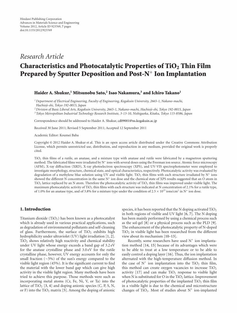
Hindawi Publishing CorporationAdvances in Materials Science and EngineeringVolume 2012, Article ID 923769, 7 pagesdoi:10.1155/2012/923769
Research Article
Characteristics and Photocatalytic Properties of TiO2 Thin FilmPrepared by Sputter Deposition and Post-N+ Ion Implantation
Haider A. Shukur,1 Mitsunobu Sato,2 Isao Nakamura,3 and Ichiro Takano1
1 Department of Electrical Engineering, Faculty of Engineering, Kogakuin University, 2665-1, Nakano-machi,Hachioji-shi, Tokyo 192-0015, Japan
2 Division of Basic Liberal Arts, Kogakuin University, 2665-1, Nakano-machi, Hachioji-shi, Tokyo 192-0015, Japan3 Tokyo Metropolitan Industrial Technology Research Institute, 3-13-10, Nishigaoka, Kitaku, Tokyo 115-8586, Japan
Correspondence should be addressed to Haider A. Shukur, [email protected]
Received 30 June 2011; Revised 5 September 2011; Accepted 12 September 2011
Academic Editor: Koumei Baba
Copyright © 2012 Haider A. Shukur et al. This is an open access article distributed under the Creative Commons AttributionLicense, which permits unrestricted use, distribution, and reproduction in any medium, provided the original work is properlycited.
TiO2 thin films of a rutile, an anatase, and a mixture type with anatase and rutile were fabricated by a magnetron sputteringmethod. The fabricated films were irradiated by N+ ions with several doses using the Freeman ion source. Atomic force microscopy(AFM), X-ray diffraction (XRD), X-ray photoelectron spectroscopy (XPS), and UV-VIS spectrophotometer were employed toinvestigate morphology, structure, chemical state, and optical characteristics, respectively. Photocatalytic activity was evaluated bydegradation of a methylene blue solution using UV and visible light. TiO2 thin films with each structure irradiated by N+ ionsshowed the different N concentration in the same N+ ion dose and the chemical state of XPS results suggested that an O atom inTiO2 lattice replaced by an N atom. Therefore the photocatalytic activity of TiO2 thin films was improved under visible light. Themaximum photocatalytic activity of TiO2 thin films with each structure was indicated at N concentration of 2.1% for a rutile type,of 1.0% for an anatase type, and of 3.8% for a mixture type under the condition of 2.5× 10¹⁵ ions/cm2 in N+ ion dose.
1. Introduction
Titanium dioxide (TiO2) has been known as a photocatalystwhich is already used in various practical applications, suchas degradation of environmental pollutants and self-cleaningof glass. Furthermore, the surface of TiO2 exhibits highhydrophilicity under ultraviolet (UV) light irradiation [1, 2].TiO2 shows relatively high reactivity and chemical stabilityunder UV light whose energy exceeds a band gap of 3.2 eVfor the anatase crystalline phase and 3.0 eV for the rutilecrystalline phase, however, UV energy accounts for only thesmall fraction (∼5%) of the sun’s energy compared to thevisible light region (45%). It is the significant current to findthe material with the lower band gap which can give highactivity in the visible light region. Many methods have beentried to achieve this purpose. Those methods were such asincorporating metal atoms (Cr, Fe, Ni, V, or Ta) into thelattice of TiO2 [3, 4] and doping anionic species (C, P, S, N,or F) into the TiO2 matrix [5]. Among the doping of anionic
species, it has been reported that the N doping activated TiO2
in both regions of visible and UV light [6, 7]. The N dopinghas been mainly performed by using a chemical process suchas the sol-gel [8] or a physical process such as the PLD [9].The enhancement of the photocatalytic property of N-dopedTiO2 in visible light has been researched from the differentview about its mechanism [10–13].
Recently, some researchers have used N+ ion implanta-tion method [14, 15] because of its advantages which wereto be able to treat at a low temperature or to be able toeasily control a doping layer [16]. Thus, the ion implantationalternated with the high-temperature diffusion method. Inthe case of N+ ion implantation into the TiO2 thin film,this method can create oxygen vacancies to increase TiO2
activity [17] and can make TiO2 response to visible lightwhen N is substituted for O in the TiO2 lattice. Improvementof photocatalytic properties of the implanted TiO2 thin filmin a visible light is due to the chemical and microstructurechanges of TiO2. Most of studies about N+ ion-implanted
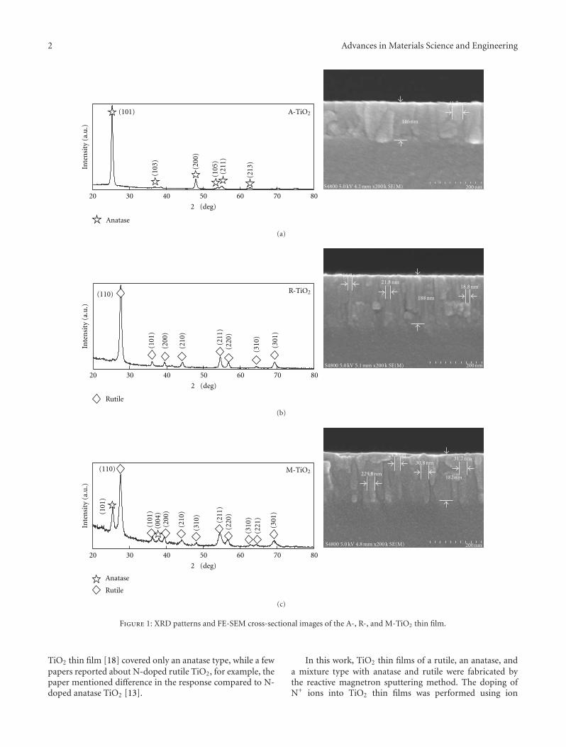
2 Advances in Materials Science and Engineering
(101)
(200
)
(211
)
(213
)
(103
)
(105
)Anatase
Inte
nsi
ty(a
.u.)
2 (deg)
A-TiO2
20 30 40 50 60 70 80
41.7 nm
146 nm
200 nmS4800 5.0 kV 4.2 mm x200 k SE(M)
(a)
Rutile
Inte
nsi
ty(a
.u.)
(110)
(101
)
(200
)
(210
)
(211
)
(310
)
(220
)
(301
)
R-TiO2
2 (deg)
20 30 40 50 60 70 80
200 nm
18.8 nm
188 nm
21.8 nm16.9 nm
S4800 5.0 kV 5.1 mm x200 k SE(M)
(b)
Inte
nsi
ty(a
.u.)
(110)
Anatase
M-TiO2
Rutile
2 (deg)
20 30 40 50 60 70 80
(101
)
(101
)(0
04)
(200
)
(210
)
(211
)
(301
)
(220
)
(221
)(3
10)
(310
)
200 nm
31.7 nm
182 nm
30.8 nm
24.8 nm
229.8 nm
S4800 5.0 kV 4.8 mm x200 k SE(M)
(c)
Figure 1: XRD patterns and FE-SEM cross-sectional images of the A-, R-, and M-TiO2 thin film.
TiO2 thin film [18] covered only an anatase type, while a fewpapers reported about N-doped rutile TiO2, for example, thepaper mentioned difference in the response compared to N-doped anatase TiO2 [13].
In this work, TiO2 thin films of a rutile, an anatase, anda mixture type with anatase and rutile were fabricated bythe reactive magnetron sputtering method. The doping ofN+ ions into TiO2 thin films was performed using ion

Advances in Materials Science and Engineering 3
beam irradiation with several N+ ion doses. The chemical,structural, morphological, and photocatalytic propertieswere reported as a function of N+ ion dose. It was expectedthat an N atom substituted for an O atom in the TiO2
lattice so that the photocatalytic property of the TiO2
thin film was improved under visible light.
2. Experimental Details
2.1. Preparation of Samples. The magnetron sputteringsource and the Freeman type ion source of the multiprocess-coating system were used to fabricate TiO2 thin films andto irradiate the TiO2 thin film by N+ ions, respectively. Thecorning glass (number 1737) substrate was fixed on theholder of the multiprocess-coating system and sputtered byAr+ ions for 10 min in order to clean the substrate. Thiscleaning was carried out in a separated chamber before thefilm fabrication process. The film deposition chamber waspumped up by a turbo molecular and a rotary pump to reachto the chamber pressure less than 1.3 × 10⁻⁵ Pa. The filmfabrication process was carried out by introducing an Ar gasof 20 sccm in a flow rate near the Ti sputtering target and byapplying an input power of 100 W. Simultaneously, an O2 gaswas introduced around the substrate at 1.5 or 2.3 sccm in aflow rate. The pressure of the film deposition chamber waskept at 8 × 10⁻² Pa in a pressure and at 573 K in a substratetemperature through the film fabrication. The Ti-sputteringrates were measured by using a quartz crystal microbalance(QCM). Those were 0.025 nm/s for 1.5 sccm and 0.009 nm/sfor 2.3 sccm in an O2 gas flow rate, respectively. Becausethe different sputtering rates resulted due to the surfaceoxidation of a Ti target, the sputtering time was calculatedfrom each deposition rate to obtain 200 nm in film thickness.The TiO2 thin film fabricated at 2.3 sccm in an O2 flow rateshowed an anatase structure (A-TiO2), while the sample with1.5 sccm showed a mixture structure (M-TiO2) of anataseand rutile. A rutile structure (R-TiO2) was obtained byannealing a mixture structure under 700◦C for 2 hours in theair.
The ion implantation was carried out by using Freemantype ion source. N+ ions were separated by using a massseparator of 45 degree. The samples of A-TiO2, R-TiO2,and M-TiO2 were irradiated under the constant ion energyof 15 kV at the constant current density of 40 μA/cm2.The different doses of 2.5 × 10¹⁵, 5 × 10¹⁵, and 7.5 ×10¹⁵ ions/cm2 were controlled by the ion irradiation time.The ion implantation process was performed at a roomtemperature with a pressure less than 1 × 10⁻⁴ Pa and anincidence angle of 0 degree.
2.2. Film Characterization Measurement. The film structurewas determined by X-ray diffraction (XRD: MAC ScienceHigh quality XG M18XCE) with CuKα (0.154 nm) radiationat an incident angle of 0.3◦. The film composition wascharacterized by X-ray photoelectron spectroscopy (XPS:ULVAC-PHI, Inc.) with a focused monochromatic Al-Kα X-ray source (1486.6 eV) and a maximum energy resolutionof 0.48 eV at Ag3d5/2. The chemical state and atomic
A-TiO2
R-TiO2
M-TiO2
nm
1.9 nm
1.56 nm
500 nm
Ra = 1.25
Ra =
Ra =
(a)
A-TiO2
R-TiO2
M-TiO2
1.6 nm
3.9 nm
2.57 nm
500 nm
Ra =
Ra =
Ra =
(b)
Figure 2: AFM top-view images of the unirradiated A-, R-, and M-TiO2 thin film (a) and the irradiated A-, R-, and M-TiO2 thin filmwith an N+ ion dose of 5.0 × 10¹⁵ ions/cm2 (b).
concentration of Ti, O, N, and C were measured andreferenced at the standard C peak. Depth profiles in theAr+ ion etching mode were obtained at 2 kV in a ionenergy and 20 μA/cm2 in a ion current for the maximum3 min. The surface morphology and the cross-section ofsamples were observed by an atomic force microscopy (AFM:Shimadzu SPM-9500) and a field-emission scanning electronmicroscope (FE-SEM: S-4800 Hitachi High-Technologiesco.), respectively. The photocatalytic property of TiO2 thinfilms was evaluated by decomposition of a methylene bluesolution (MB, C16H18ClN3S) of 10 ppm in a quartz cell witha size of 10 × 10 × 50 mm. The sample with an area of100 mm2 was immersed in an MB solution of 3 mL. UVlight was irradiated to the sample by using a commercialsterilization lamp (S.L.) with a main wavelength of 280 nmand a light intensity of 0.088 mW/cm2 at 360 nm. Artificialsunlight lamp (A.L.) with a UV cut-off filter (under 350 nm)was also irradiated on the sample at a light intensity of0.228 mW/cm2 at 360 nm. After the light irradiation, thechange of a decolorized MB solution was calculated by

4 Advances in Materials Science and Engineering
Inte
nsi
ty(a
.u.)
2 (deg)
(101)
(200
)(2
11)
(213
)
(103
)
(105
)
Anatase
7.5 × 10¹⁵ ions/cm2
5 × 10¹⁵ ions/cm2
2.5 × 10¹⁵ ions/cm2
A-TiO2
Un-irradiated
20 40 60 80
(a)
Inte
nsi
ty(a
.u.)
2 (deg)
Un-irradiated
20 40 60 80
(110)
(101
)(2
00)
(210
)
(211
)
(310
)
(220
)
Rutile
R-TiO2
7.5 × 10¹⁵ ions/cm2
5 × 10¹⁵ ions/cm2
2.5 × 10¹⁵ ions/cm2
(b)
Inte
nsi
ty(a
.u.)
2 (deg)
Un-irradiated
20 40 60 80
Rutile
7.5 × 10¹⁵ ions/cm2
5 × 10¹⁵ ions/cm2
2.5 × 10¹⁵ ions/cm2
Anatase
(101
)
(110)
(101
)(0
04)
(200
)(2
10)
(220)(221) (310)
M-TiO2
(c)
Figure 3: XRD patterns of the unirradiated A-, R-, and M-TiO2 thin film and the irradiated A-, R-, and M-TiO2 thin film with an N+ iondose of 2.5 × 10¹⁵, 5.0 × 10¹⁵, and 7.5 × 10¹⁵ ions/cm2.
measuring the transmittance of the MB solution usinga spectrophotometer (UV-2550, Shimadzu co.) at regularintervals.
3. Results and Discussion
3.1. Surface Morphology and Structure. Figure 1 shows XRDpatterns and cross-sectional images of each TiO2 thin filmwith different structure. The XRD pattern of the A-TiO2
thin film showed the strong peak of anatase (101) withouta rutile structure and that of the R-TiO2 thin film showedthe strong peak of rutile (110), while the M-TiO2 thin filmhad the double strong peaks of anatase (101) and rutile(110). According to the cross-sectional images, the thicknessof the A-TiO2 thin film was 146 nm due to decrease of thesputtering rate by of the high O2 gas flow rate at the filmfabrication, while the thickness of the R-TiO2 thin film andthe M-TiO2 thin film was 188 and 182 nm, respectively. EachTiO2 thin film showed a columnar structure. The A-TiO2
thin film had the grain size of about 40 nm because of thehigh crystalline. That of the R-TiO2 and the M-TiO2 thin filmwere 16.9–21.8 nm and 24.8–31 nm, respectively.
AFM images of a tapping mode clarified the roughness(Ra) and the morphology of each TiO2 thin film with thedifferent structure and post-N+ ion irradiation. Figure 2shows the top views of A-, R-, and M-TiO2 thin films (a)and those of films irradiated by N+ ions with a dose of 5 ×10¹⁵ ions/cm2 (b). It was clear that the morphology of theA-TiO2 thin film was different from the R- and the M-TiO2
thin film. The morphology of the A-TiO2 thin film was anaggregate of spherical particles with the number of 22–25
per 1.0 μm in the length. This spherical size correspondedto the grain size of 40–45.45 nm as observed in the cross-sectional images. The R- and the M-TiO2 thin film showssmall spherical grains and a large roughness compared withthe A-TiO2 thin film. These small grain sizes of 25–33.3 nmwere calculated from spherical particle numbers of 30–40 per1.0 μm and were slightly larger than the size indicated in thecross-section images of the R- and the M-TiO2 thin film.
The roughness of N+ ion-irradiated TiO2 thin films waslarger than that of unirradiated TiO2 thin films. The sur-face of each unirradiated TiO2 thin film was roughed bysputtering of N+ ion irradiation. The surface of the N+ ion-irradiated R- and A-TiO2 thin film showed a smaller grainsize compared with the unirradiated thin film, while thesurface of the M-TiO2 thin film turned to a larger grain sizeby N+ ion irradiation. These surface changes of the irradiatedTiO2 thin film were influenced by an N+ ion dose and anion projected range. It was considered that the increase ofthe grain size of the N+ ion-irradiated M-TiO2 thin film wasinfluenced by a high N concentration in the thin film.
Figure 3 shows the XRD patterns of the unirradiatedA-, R-, and M-TiO2 thin film and the irradiated A-, R-,and M-TiO2 thin film prepared with several N+ ion doses.The structure of the A-TiO2 thin film declined with N+
ion irradiation as the drastic decrease of the anatase peak(101) showed, while the rutile peak (110) of the R-TiO2
thin film showed no large change for N+ ion irradiationbecause of thermostability of a rutile type. It is generallyknown that the ion implantation method courses physicaland thermal influence to a substrate. The lattice damage dueto collisions between the ions and the lattice atoms stimulatesrecombination and the kinetic energy of implanted ions is

Advances in Materials Science and Engineering 5
Table 1: O, Ti, and N atomic concentration of the A-, R-, and M-TiO2 thin films under several N+ ion doses.
Atomic con.
N+ ion dose A-TiO2 (%) R-TiO2 (%) M-TiO2 (%)
O Ti N O Ti N O Ti N
2.5 × 10¹⁵ ions/cm2 75.8 22.1 2.1 68.5 30.5 1.0 73.6 22.7 3.8
5.0 × 10¹⁵ ions/cm2 71.3 23.2 5.5 67.0 29.1 3.9 68.6 23.2 8.3
7.5 × 10¹⁵ ions/cm2 67.6 21.9 10.5 64.1 30.6 5.3 63.2 22.0 14.9
Inte
nsi
ty(a
.u.)
Binding energy (eV)
M-TiO2
R-TiO2
A-TiO2
Un-irradiated
Ti2p1/2464.34 eV
Ti2pTi2p3/2458.84 eV
454 458 462 466 470
(a)
Inte
nsi
ty(a
.u.)
M-TiO2
R-TiO2
A-TiO2
399.1 eVN1s
Binding energy (eV)
394 396 398 400 402 404
(b)
Figure 4: XPS Ti2p and N1s spectra of unirradiated TiO2 thin filmand the irradiated A-, R-, and M-TiO2 thin film with an N+ ion doseof 5.0 × 10¹⁵ ions/cm2.
converted to thermal energy. N+ ion irradiation played amain role to change the structure from anatase to mixture[16]. In the XRD pattern of the A-TiO2 thin film, the smallrutile peak (110) started to appear with an N+ ion dose.Furthermore, in the case of the M-TiO2 thin film the XRDpattern showed decrease of the anatase peak (101) withincreasing of an N+ ion dose. The change of XRD patternsfor each TiO2 depended on thermostability of TiO2 structuretype.
3.2. Chemical State. Figure 4 shows XPS Ti2p and N1sspectra of the unirradiated TiO2 thin film and the irradiatedA-, R- and M-TiO2 thin film with an N+ ion dose of 5.0× 10¹⁵ ions/cm2, respectively. These spectra were measuredat the sample surface without an Ar+ ion etching process.N1s peaks of all N+ ion-irradiated TiO2 thin films weredetected at 399.1 eV in a binding energy. Since the peak oftitanium nitride appeared at 396.0 eV according to the XPScatalog data, it was estimated that these peaks of 399.1 eVwere caused by the Ti–O–N linkage assigned as an atomic β-N state. Therefore, these results suggested that the implantedN was incorporated into the TiO2 lattice and substitutedfor O [19–22]. This was also proved by results of the Ti2pXPS spectra because the Ti2p peak decreased and slightlyshifted to the high binding energy side by N+ ion irradiationas indicating that Ti–O bonding was accompanied by Ti–N
bonding [23], and, moreover, the O atomic concentrationwas decreased by increasing N+ ion dose as shown in Table 1,which showed the atomic concentrations of O, Ti, and Nin the N+ ion irradiated A-, R-, and M-TiO2 thin film withseveral N+ ion doses. N concentration in each thin filmwas proportional to N+ ion dose with an evidenced distinctdifference according to the TiO2 structure type. The M-TiO2
thin film included a larger N concentration compared withthe A- or R-TiO2 thin film while the smaller N concentrationwas indicated at the R-TiO2 thin film. The value of implantedN was influenced by a crystalline and a density of the TiO2
thin film, since the density of the TiO2 bulk was taken as3.86 g cm−3 for a rutile type and was smaller by 8.7% for ananatase type [24]. It is well known that the deposited filmhad a lower density depending on the deposition parametersthan the bulk material [25].
3.3. Photocatalytic Property. The photocatalytic property wasinvestigated by decomposition of an MB solution. The MBsolution exhibited an initial transmittance of 2.0% and amain absorption wavelength of 664 nm. Figure 5 shows thelight transmittance change of 664 nm as the decompositionrate of the MB solution after 6 hours for the unirradiatedA-, R-, M-TiO2 thin film and those N+ ion irradiated thinfilms. The transmittance under S.L. of the unirradiated TiO2
thin film showed larger activity than those of all N+ ion-irradiated TiO2 thin films. It was clear that the effect of N+
ion irradiation under S.L. did not show because the defectof the TiO2 lattice by the ion beam collision was generatedand the effect of N+ ion dose for UV light was not originallyanticipated. On the other hand, all N+ ion irradiated TiO2
thin films showed increase of the transmittance underA.L. with N+ ion irradiation, however, the transmittancedecreased by an excess of an N+ ion dose. From these results,the maximum photocatalytic activity of the A-, R-, and M-TiO2 thin film was indicated at an N+ ion dose of 2.5 ×10¹⁵ ions/cm2.
4. Conclusions
Three different structures of anatase, rutile, and mixture asTiO2 thin films were prepared by the reactive magnetronsputtering method. N+ ion beam with several doses wasirradiated to TiO2 thin films with three different structuresin a room temperature. Structural, morphological, chemical,and photocatalytic properties were investigated about unir-radiated and N+ ion irradiated thin films. The anatase (101)peak was weakened by N+ ion irradiation, while the rutile

6 Advances in Materials Science and Engineering
0
10
20
30
40
50
60
70
80
90
100
0
5
10
15
S.L.
tra
nsm
itta
nce
(%
)
A.L
. tra
nsm
itta
nce
(%
)
0 2.5 5 7.5
A-TiO2
N+ ion dose (× 1015 ions/cm2)
(a)
0
10
20
30
40
50
60
70
80
90
100
0
5
10
15
0 2.5 5 7.5
R-TiO2
N+ ion dose (× 1015 ions/cm2)
S.L.
tra
nsm
itta
nce
(%
)
A.L
. tra
nsm
itta
nce
(%
)
(b)
A.L.S.L.
0
10
20
30
40
50
60
70
80
90
100
0
5
10
15
0 2.5 5 7.5
M-TiO2
N+ ion dose (× 1015 ions/cm2)
S.L.
tra
nsm
itta
nce
(%
)
A.L
. tra
nsm
itta
nce
(%
)
(c)
Figure 5: Transmittance changes of the methylene blue solution under sterilization lamp (S.L.) as UV light and artificial lamp (A.L.) asvisible light for the unirradiated A-, R-, and M-TiO2 thin film and the irradiated A-, R-, and M-TiO2 thin film with an N+ ion dose of 2.5 ×10¹⁵, 5.0 × 10¹⁵, and 7.5 × 10¹⁵ ions/cm2.
(110) peak had no large change against N+ ion irradiation.N1s spectra of all N+ ion irradiated A-, R-, and M-TiO2
thin films had the peaks at 399.1 eV corresponding to Ti–O–N bonding; however, N concentration for each structureshowed a different value in spite of the irradiation with thesame N+ ion dose. It became clear that N+ ion implantationrate was different by TiO2 structure type. Incorporation ofN into the TiO2 lattice by substituting for O was confirmedby XPS results and played the great role to improve thephotocatalytic activity of the TiO2 thin film under visiblelight.
References
[1] A. Fujishima and K. Honda, “Electrochemical photolysis ofwater at a semiconductor electrode,” Nature, vol. 238, no.5358, pp. 37–38, 1972.
[2] R. Wang, K. Hashimoto, A. Fujishima et al., “Light-inducedamphiphilic surfaces,” Nature, vol. 388, no. 6641, pp. 431–432,1997.
[3] M. Anpo and M. Takeuchi, “The design and development ofhighly reactive titanium oxide photocatalysts operating undervisible light irradiation,” Journal of Catalysis, vol. 216, no. 1-2,pp. 505–516, 2003.

Advances in Materials Science and Engineering 7
[4] S. T. Martin, H. Herrmann, W. Choi, and M. R. Hoffmann,“Time-resolved microwave conductivity. Part 1.—TiO2 pho-toreactivity and size quantization,” Journal of the ChemicalSociety, Faraday Transactions, vol. 90, no. 21, pp. 3315–3322,1994.
[5] T. Ihara, M. Miyoshi, M. Ando, S. Sugihara, and Y. Iriyama,“Preparation of a visible-light-active TiO2 photocatayst by RFplasma treatment,” Journal of materials science, vol. 36, no. 17,pp. 4201–4207, 2001.
[6] R. Asahi, T. Morikawa, T. Ohwaki, K. Aoki, and Y. Taga,“Visible-light photocatalysis in nitrogen-doped titaniumoxides,” Science, vol. 293, no. 5528, pp. 269–271, 2001.
[7] Y. Sakatani and H. Koike, Japan Patent P2001-72419A, 2001.[8] S. K. Zheng, T. M. Wang, W. C. Hao, and R. Shen, “Improve-
ment of photocatalytic activity of TiO2 thin film by Sn ionimplantation,” Vacuum, vol. 65, no. 2, pp. 155–159, 2002.
[9] Y. Suda, H. Kawasaki, T. Ueda, and T. Ohshima, “Preparationof high quality nitrogen doped TiO2 thin film as a photocata-lyst using a pulsed laser deposition method,” Thin Solid Films,vol. 453-454, pp. 162–166, 2004.
[10] K. Yang, Y. Dai, B. Huang, and S. Han, “Theoretical study ofN-doped TiO2 rutile crystals,” Journal of Physical Chemistry B,vol. 110, no. 47, pp. 24011–24014, 2006.
[11] J. Graciani, L. J. Alvarez, J. A. Rodriguez, and J. F. Sanz, “Ndoping of rutile TiO2 (110) surface. A theoretical DFT study,”Journal of Physical Chemistry C, vol. 112, no. 7, pp. 2624–2631,2008.
[12] C. Di Valentin, G. Pacchioni, A. Selloni, S. Livraghi, and E.Giamello, “Characterization of paramagnetic species in N-doped TiO2 powders by EPR spectroscopy and DFT calcul-ations,” Journal of Physical Chemistry B, vol. 109, pp. 11414–11419, 2005.
[13] S. Livraghi, A. M. Czoska, M. C. Paganini, and E. Giamello,“Preparation and spectroscopic characterization of visiblelight sensitized N doped TiO2 (rutile),” Journal of Solid StateChemistry, vol. 182, no. 1, pp. 160–164, 2009.
[14] R. Fernandes, N. Patel, R. Dholam, M. Adami, and A. Miotello,“Low energy ion-beam modification of TiO2 photocatalystthin film for visible light absorption,” Surface and CoatingsTechnology, vol. 203, no. 17-18, pp. 2579–2583, 2009.
[15] S. K. Zheng, T. M. Wang, W. C. Hao, and R. Shen, “Improve-ment of photocatalytic activity of TiO2 thin film by Sn ionimplantation,” Vacuum, vol. 65, no. 2, pp. 155–159, 2002.
[16] B. G. Streeetman and S. Banerjee, Solid State ElectronicsDevices, Prentice Hall, Upper Saddle River, NJ, USA, 5thedition, 2000.
[17] I. Nakamura, N. Negishi, S. Kutsuna, T. Ihara, S. Sugihara, andK. Takeuchi, “Role of oxygen vacancy in the plasma-treatedTiO2 photocatalyst with visible light activity for NO removal,”Journal of Molecular Catalysis A, vol. 161, no. 1-2, pp. 205–212,2000.
[18] P. Romero-Gomez, A. Palmero, F. Yubero, M. Vinnichenko, A.Kolitsch, and A. R. Gonzalez-Elipe, “Surface nanostructuringof TiO2 thin films by ion beam irradiation,” Scripta Materialia,vol. 60, no. 7, pp. 574–577, 2009.
[19] R. Asahi, T. Morikawa, T. Ohwaki, K. Aoki, and Y. Taga,“Visible-light photocatalysis in nitrogen-doped titanium oxi-des,” Science, vol. 293, no. 5528, pp. 269–271, 2001.
[20] R. Knizikevicius, “Simulation of reactive sputter depositionof TiO2 films,” Materials Science, vol. 16, no. 3, pp. 202–204,2010.
[21] C. Burda, Y. Lou, X. Chen, A. C. S. Samia, J. Stout, and J.L. Gole, “Enhanced nitrogen doping in TiO2 nanoparticles,”Nano Letters, vol. 3, no. 8, pp. 1049–1051, 2003.
[22] M. Xing, J. Zhang, and F. Chen, “New approaches toprepare nitrogen-doped TiO2 photocatalysts and study ontheir photocatalytic activities in visible light,” Applied CatalysisB, vol. 89, no. 3-4, pp. 563–569, 2009.
[23] P. G. Wu, C. H. Ma, and J. K. Shang, “Effects of nitrogendoping on optical properties of TiO2 thin films,” AppliedPhysics A, vol. 81, no. 7, pp. 1411–1417, 2005.
[24] N. Matsunami, M. Uebayashi, K. Hirooka, T. Shimura, andM. Tazawa, “N ion irradiation enhancement of photocatalyticactivity of TiO2,” Nuclear Instruments and Methods in PhysicsResearch, Section B, vol. 267, no. 8-9, pp. 1654–1657, 2009.
[25] W. Wagner, F. Rauch, and K. Bange, “Concentration profilesof hydrogen in technical oxidic thin films and multilayersystems,” Fresenius’ Zeitschrift fur Analytische Chemie, vol. 333,no. 4-5, pp. 478–480, 1989.

Hindawi Publishing CorporationAdvances in Materials Science and EngineeringVolume 2012, Article ID 826873, 13 pagesdoi:10.1155/2012/826873
Review Article
Nonstoichiometry in TiO2−y Studied byIon Beam Methods and Photoelectron Spectroscopy
K. Zakrzewska
Faculty of Electrical Engineering, Automatics, Computer Science and Electronics, AGH University of Science and Technology,30 Mickiewicza Avenue, 30-059 Krakow, Poland
Correspondence should be addressed to K. Zakrzewska, [email protected]
Received 7 July 2011; Revised 30 August 2011; Accepted 1 September 2011
Academic Editor: Adam Georg Balogh
Copyright © 2012 K. Zakrzewska. This is an open access article distributed under the Creative Commons Attribution License,which permits unrestricted use, distribution, and reproduction in any medium, provided the original work is properly cited.
This paper treats a problem of nonstoichiometry in TiO2−y thin films deposited by reactive sputtering at controlled sputteringrates. Ion beam techniques, Rutherford backscattering (RBS), and nuclear reaction analysis (NRA) along with X-ray photoelectronspectroscopy have been applied to determine a deviation from stoichiometry y in the bulk and at the surface of TiO2−y layers. Thecritical review of these experimental methods is given. Defect structure responsible for the electrical resistivity of rutile TiO2 isdiscussed.
1. Introduction
Titanium dioxide is considered as one of the most importantmaterials from the point of view of both fundamentalproperties and applications. These applications rely on excel-lent chemical stability of TiO2 in hazardous environments,hardness, high refractive index, and many other remarkablefeatures.
Titanium dioxide TiO2 exists in three polymorphic forms:brookite, rutile, and anatase. Anatase and brookite as me-tastable phases transform irreversibly into rutile over thetemperature range of 973 K–1173 K [1].
Rutile is a high-temperature, stable phase, thus it is notsurprising that this particular polymorphic form has beenthe most thoroughly investigated. The majority of crystalgrowth techniques yield titanium dioxide in the rutile phase.Moreover, in many devices (e.g., gas sensors) that operate athigh temperatures, TiO2 is already converted into rutile.
Recently, less common anatase has gained a considerablescientific importance thanks to a significant role it playsin photocatalytic, photovoltaic, and photoelectrochemicalapplications of titanium dioxide [2]. Some basic physicalparameters such as the bandgap, effective mass, and mobilityof charge carriers, assumed earlier to be the same as inrutile, in fact were found to differ considerably in the caseof anatase.
Titanium dioxide due to its wide band gap (3.0 eV forrutile and 3.2 eV for anatase [1]) should be treated as aninsulator. However, when equilibrated in an atmosphere oflow oxygen activity, it becomes an oxygen-deficient sem-iconductor due to the electronic disorder related to nonstoi-chiometry [3].
Much work has been devoted to the nonstoichiometricrutile TiO2−y , both in the structural aspects related to thenature of defects [4, 5] and in the subsequent physical [6, 7]and thermodynamic properties [8]. However, there is stilla disagreement as to the extent of nonstoichiometry andthe mechanism by which it is accommodated in rutile. It isgenerally believed that titania can support large deviationsfrom stoichiometry. Earlier investigations overestimated thehomogeneity range of TiO2−y extending it to a value as highas y ∼= 0.1 at 1170–1270 K [8]. Later experimental evidence[9] suggests that the homogeneity range is much narrower(y ∼= 0.008 at 1270 K).
The structure of defects responsible for the electronicconduction in rutile and anatase TiO2 is still a subject ofdiscussion in spite of numerous studies devoted to this topicand the varied experimental techniques used to determineit. It is often assumed that oxygen deficiency could beaccommodated by point defects: oxygen vacancies [10],titanium interstitials [11, 12], or a combination of these twodefects [13]. Ionization of these defects provides electrons

2 Advances in Materials Science and Engineering
necessary for the electrical conduction. Which particulardefect is responsible for the electrical conductivity is largelyaffected by the conditions of experiment. The majority ofdefects switch their role when scanning over the temperatureand oxygen partial pressure ranges as shown in [14].
It should be pointed out that there exists a significantcontroversy between two different approaches to the problemof defects in rutile. Some authors [4] claim that even for anextremely small departure from the ideal composition, non-stoichiometry is accommodated mainly by a crystallographicshear plane mechanism while the point defects model maybe applied very close to the stoichiometric composition only.
Randomly distributed point defects of low density,present when the deviation from stoichiometry is small,become ordered as their concentration and interactionbetween them increase. In rutile (TiO2) this ordering takesa form of planar defects, that is, crystallographic shear (CS)planes. The planar defects, when numerous enough, orderto form new compounds with distinct compositions andstructures known as Magneli phases [5]. Magneli phasesconstitute a homologous series with the general formulaTi jO2 j−1, where j is related by j = 1/y to a deviation fromstoichiometry y (TiO2−y).
Phase diagram of Ti–O system [1] indicates that theregion of 0.1 ≤ y ≤ 0.25 contains stable ordered phasesTi jO2 j−1 with 4 ≤ j ≤ 10. For smaller departures fromstoichiometry y < 0.1 (10 < j < 16) the concentrationof the shear planes defects decreases and their mutualinteraction becomes weaker. For a very small departure fromstoichiometry, y ∼= 0.001, corresponding to j > 1000,formation of isolated shear planes in equilibrium with pointdefects was proposed [15]. This is described as a Wadsleydefect.
A detailed description of the mechanism of nucleation,growth, and aggregation of the shear planes CS is beyond thescope of this work but may be found in numerous papersdevoted to this problem [4, 5, 16]. Existence of such defectsin single crystals has been confirmed experimentally by STM[17] and TEM [18].
The experimental results of tracer diffusion [12], chem-ical diffusion [11], and thermogravimetric measurements[19] indicate titanium interstitials as the majority pointdefects in oxygen-deficient TiO2−y . Works in favour of oxy-gen vacancies are also numerous. The computer simulationof the defect chemistry of rutile TiO2 has been carried out aswell [20].
This issue in the case of anatase has been only quiterecently brought up [21, 22]. Na-Phattalung et al. [21] per-forming first-principle calculations have found that theformation energy of oxygen vacancies is higher than that oftitanium interstitials. Thus, in undoped samples, titaniuminterstitials should be the leading donors while postgrowthformation of oxygen vacancies is also possible upon heating.
A transition from predominant oxygen vacancies totitanium interstitials in anatase has been reported byWeibel et al. [22] on the basis of the measurements of theelectrical resistivity in dense anatase ceramics. This transitionhas been observed upon the temperature increase and/orthe oxygen partial pressure decrease. Hence, it could be
Table 1: Theoretical analysis of point defects formation in TiO2−y .
Majority defect Reaction of formationTheoreticalvalue of my
Doubly ionizedoxygen vacancy V••O
OxO ←→
12
O2(g) + V••O + 2e′ 6
Singly ionizedoxygen vacancy V•O
OxO ←→
12
O2(g) + V•O + e′ 4
Titaniuminterstitial Ti4+
iTixTi +2Ox
O ←→ Ti4+i +4e′+O2(g) 5
Titaniuminterstitial Ti3+
iTixTi +2Ox
O ←→ Ti3+i +3e′+O2(g) 4
concluded that the formation of titanium interstitials wasmore favourable in anatase in comparison to rutile due tolower density of anatase than that of rutile.
The aim of this work is to review the problem ofexperimental techniques best suited to the determination ofdeviation from stoichiometry y in TiO2−y thin films. Thinfilms were deposited by rf and dc magnetron sputteringtechnique. The sputtering conditions are well defined in sucha sense that the substrate temperature and sputtering ratewere continuously controlled as described in detail in [23].
2. Electrical Conductivity and Point DefectStructure of TiO2−y
The departure from stoichiometry y may be expressed withinthe ideal mass action law as a function of the oxygen partialpressure pO2 :
y ∝ pO2−1/my , (1)
where my yields information on the nature of the defectstructure [24].
The following types of defects: doubly V••O and singlyV•O ionized oxygen vacancies as well as titanium interstitialsTi3+
i and Ti4+i are usually taken into account. Theoretically
predicted values of my associated with the specific pointdefect are listed in Table 1. When dealing with the structureof point defects, the Kroger-Vink notation [25] is used.
The electrical conductivity of titanium dioxide is afunction of the temperature, T , and oxygen partial pressure,pO2 . The latter is a consequence of the relation between thedeparture from stoichiometry y and pO2 given by (1).
The temperature dependence of the carrier concentra-tion and conductivity for nonstoichiometric TiO2−y involvesthe activation energy Ea of the conduction process, associ-ated with ionization of certain neutral defects. As oxygenvacancies usually form shallow donor levels, their activationenergy is much smaller than the forbidden band gap Egand a measurable value of the electrical conductivity can beobserved even at room temperature for nonstoichiometricTiO2−y .
The experimental evidence shows that at high oxygenpartial pressures pO2 , close to 0.1 MPa and below 1200 K,TiO2 exhibits an n-p-type transition [3, 26, 27].

Advances in Materials Science and Engineering 3
In the n-type regime, the electrical conductivity σ ofTiO2−y is affected by the oxygen partial pressure pO2
σ ∝ pO2−1/mσ . (2)
This is due to the fact that the electron concentration ne
is a function of pO2
ne ∝ pO2−1/mn , (3)
which results from the relationship between ne and thedeparture from stoichiometry y. When the mobility ofcharge carriers is independent of the oxygen partial pressure,then mn = mσ .
The coefficients my , mn, and mσ can be calculated fromthe appropriate models of point defects. Experimentally, theycan be determined from the relations given by (1), (2), or(3) by measuring y, ne, or σ , respectively, as a function ofoxygen partial pressure pO2 . As shown in Figure 1, the slopeof σ(pO2 ) dependence plotted in the double logarithmiccoordinate system yields the coefficient mσ . According to theanalysis presented in Table 1, it should be possible on thisbasis to discriminate between different types of defects anddetermine the majority defect mechanism.
In practice, the electrical measurements in TiO2 over thetemperature range of 1070–1370 K reveal [14] that the slopeof log σ against log pO2 is different under different regimesof oxygen activities. Therefore, the parameter mσ associatedwith the majority defect, changes when pO2 is varied. At lowoxygen partial pressures mσ close to 5 is obtained whichcan be accounted for by titanium interstitials, Ti4+
i . Overthe intermediate range of pO2 , mσ = 6 and doubly ionizedoxygen vacancies V••O are postulated. Finally, at high pO2
the value close to 4 is observed, corresponding to eithersingly ionized oxygen vacancy defect, V•O, or interstitial tita-nium, Ti3+
i .In the n-p-type transition region, two competitive defect
models have been proposed [26, 27]. One is related tothe extrinsic disorder and assumes that the acceptor-typeimpurities are always present in TiO2. The second modelconsiders the Schottky-type defect comprising the titaniumvacancy V////
Ti associated with oxygen vacancy V••O . Bothmodels give the same dependence of concentration ofelectrons (ne) and that of holes (nh) on pO2 :
ne ∝ pO2−1/4,
nh ∝ pO21/4.
(4)
The p-type conductivity in TiO2 is predicted to occurunder very high partial pressure of oxygen. The same twomodels: extrinsic disorder and Schottky-type defect arediscussed in this case [26]. The former assumes that theconcentration of holes is much larger than that of oxygenvacancies. The latter requires the concentration of holes to becompensated by V////
Ti . The results of these models are quitedifferent. The extrinsic disorder yields the concentration ofholes independent of the pO2 [26]. The Schottky model gives[26]
nh ∝ pO21/5. (5)
10− 15 10− 10 10− 5 10510010− 3
10− 2
10− 1
100
101
(oh
m−
1cm
−1)
pO2(Pa)
thin film
single crystal
− 800
− 600
− 400
− 200
0
200
400
600
Q single crystal
Q(μ
V/K
)
Figure 1: Electrical conductivity σ measured at 1250 K as a functionof the oxygen partial pressure pO2 for a thin film of TiO2−y . Theresults of σ and Seebeck coefficient Q concern rutile single crystal.
The arguments leading to the relation described aboveassume a quite unrealistic situation in which only one typeof defect is present. In practice, under the experimentalconditions of pO2 ≤ 105 Pa the dependence given by (4) isobserved instead.
The following comments to the analysis presented aboveshould be taken into account.
(i) Unambiguous assignment of the majority defect onthe basis of mσ is difficult to make because frequentlythe same value of this parameter corresponds to morethan one type of defect. This is the case for mσ = 4related to the singly ionized oxygen vacancy or thetitanium interstitial.
(ii) Different types of majority defects predominate overdifferent ranges of oxygen partial pressure.
(iii) One should expect the combination of point defectsrather than a single defect to be present in TiO2−y .
In fact, the coexistence of divalent oxygen vacancies withtri- and tetravalent titanium interstitials has been proposed[13].
3. Nonstoichiometric Thin Films of TiO2−y
A variety of deposition techniques including chemical(CVD) [28–31] and physical vapour deposition (PVD) [32–34] have been reported for titanium dioxide thin films.One should mention here growth techniques successfullyapplied in the elaboration of TiO2 thin films, such as sol-gel process [35], atomic layer epitaxy (ALE) [36], pulsedlaser deposition [37], and filtered arc deposition (FAD)[38]. Excellent reviews, covering both the growth techniquesapplied to deposition of TiO2 coatings as well as the film
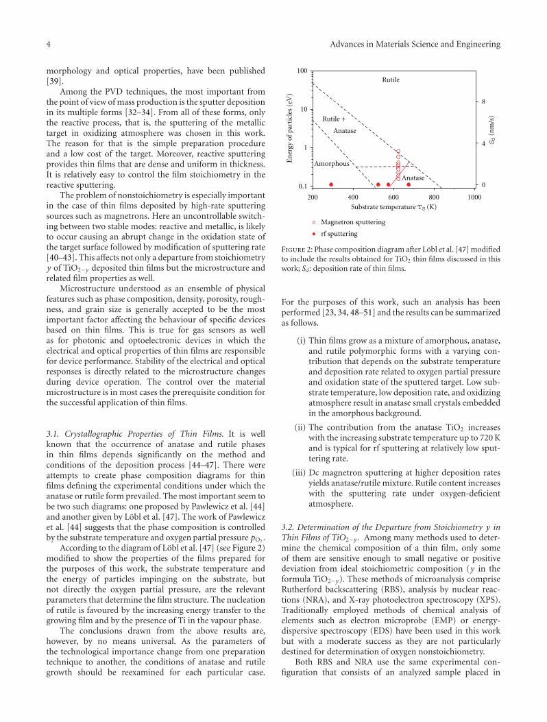
4 Advances in Materials Science and Engineering
morphology and optical properties, have been published[39].
Among the PVD techniques, the most important fromthe point of view of mass production is the sputter depositionin its multiple forms [32–34]. From all of these forms, onlythe reactive process, that is, the sputtering of the metallictarget in oxidizing atmosphere was chosen in this work.The reason for that is the simple preparation procedureand a low cost of the target. Moreover, reactive sputteringprovides thin films that are dense and uniform in thickness.It is relatively easy to control the film stoichiometry in thereactive sputtering.
The problem of nonstoichiometry is especially importantin the case of thin films deposited by high-rate sputteringsources such as magnetrons. Here an uncontrollable switch-ing between two stable modes: reactive and metallic, is likelyto occur causing an abrupt change in the oxidation state ofthe target surface followed by modification of sputtering rate[40–43]. This affects not only a departure from stoichiometryy of TiO2−y deposited thin films but the microstructure andrelated film properties as well.
Microstructure understood as an ensemble of physicalfeatures such as phase composition, density, porosity, rough-ness, and grain size is generally accepted to be the mostimportant factor affecting the behaviour of specific devicesbased on thin films. This is true for gas sensors as wellas for photonic and optoelectronic devices in which theelectrical and optical properties of thin films are responsiblefor device performance. Stability of the electrical and opticalresponses is directly related to the microstructure changesduring device operation. The control over the materialmicrostructure is in most cases the prerequisite condition forthe successful application of thin films.
3.1. Crystallographic Properties of Thin Films. It is wellknown that the occurrence of anatase and rutile phasesin thin films depends significantly on the method andconditions of the deposition process [44–47]. There wereattempts to create phase composition diagrams for thinfilms defining the experimental conditions under which theanatase or rutile form prevailed. The most important seem tobe two such diagrams: one proposed by Pawlewicz et al. [44]and another given by Lobl et al. [47]. The work of Pawlewiczet al. [44] suggests that the phase composition is controlledby the substrate temperature and oxygen partial pressure pO2 .
According to the diagram of Lobl et al. [47] (see Figure 2)modified to show the properties of the films prepared forthe purposes of this work, the substrate temperature andthe energy of particles impinging on the substrate, butnot directly the oxygen partial pressure, are the relevantparameters that determine the film structure. The nucleationof rutile is favoured by the increasing energy transfer to thegrowing film and by the presence of Ti in the vapour phase.
The conclusions drawn from the above results are,however, by no means universal. As the parameters ofthe technological importance change from one preparationtechnique to another, the conditions of anatase and rutilegrowth should be reexamined for each particular case.
200 400 600 800 1000
0.1
1
10
100
Amorphous
Anatase
Rutile +
Anatase
En
ergy
ofpa
rtic
les
(eV
)
Substrate temperature TS (K)
Rutile
0
4
8
Magnetron sputtering
rf sputtering
S d(n
m/s
)
Figure 2: Phase composition diagram after Lobl et al. [47] modifiedto include the results obtained for TiO2 thin films discussed in thiswork; Sd : deposition rate of thin films.
For the purposes of this work, such an analysis has beenperformed [23, 34, 48–51] and the results can be summarizedas follows.
(i) Thin films grow as a mixture of amorphous, anatase,and rutile polymorphic forms with a varying con-tribution that depends on the substrate temperatureand deposition rate related to oxygen partial pressureand oxidation state of the sputtered target. Low sub-strate temperature, low deposition rate, and oxidizingatmosphere result in anatase small crystals embeddedin the amorphous background.
(ii) The contribution from the anatase TiO2 increaseswith the increasing substrate temperature up to 720 Kand is typical for rf sputtering at relatively low sput-tering rate.
(iii) Dc magnetron sputtering at higher deposition ratesyields anatase/rutile mixture. Rutile content increaseswith the sputtering rate under oxygen-deficientatmosphere.
3.2. Determination of the Departure from Stoichiometry y inThin Films of TiO2−y . Among many methods used to deter-mine the chemical composition of a thin film, only someof them are sensitive enough to small negative or positivedeviation from ideal stoichiometric composition (y in theformula TiO2−y). These methods of microanalysis compriseRutherford backscattering (RBS), analysis by nuclear reac-tions (NRA), and X-ray photoelectron spectroscopy (XPS).Traditionally employed methods of chemical analysis ofelements such as electron microprobe (EMP) or energy-dispersive spectroscopy (EDS) have been used in this workbut with a moderate success as they are not particularlydestined for determination of oxygen nonstoichiometry.
Both RBS and NRA use the same experimental con-figuration that consists of an analyzed sample placed in

Advances in Materials Science and Engineering 5
a monoenergetic beam of protons, deuterons, or heliumions, typically 4He++ [52–57]. Particles coming from thebombarded sample as a result of the interaction of the beamand the elements in the sample are detected and analyzed. Inthe case of RBS, it is the energy of the backscattered particlesthat dissipated their incident energy by elastic (Rutherford)collisions, while for NRA, the energy of the reaction productsis analyzed. XPS is a method that makes use of the X-rayradiation to excite electrons from the core levels of atoms[58]. Kinetic energy of the photoelectrons measured directlyin XPS is related to their binding energy in atoms, which inturn is sensitive to the atom environment. The chemical shiftin the binding energy forms a basis for the identification ofelements and their oxidation states in the specific chemicalcompounds.
RBS and NRA measurements were carried out at a beamline of the 2 MeV Van de Graaff accelerator being at thedisposition of GIP (Groupe de Physique des Solides) at EcoleNormale Superieure, in collaboration with LOS (Laboratoired’Optique des Solides) Universite P. et M. Curie, Paris 6,France, described in detail in [54]. The energy of particleswas measured with a silicon surface-barrier detector andthe signals were analyzed with a multichannel analyzer.Complementary RBS measurements were performed atCalifornia Institute of Technology CalTech, USA. In thiswork, the RBS experiments were done mostly with alphaparticles 4He++ of the incident energy E0 = 2.012 MeV or1.96 MeV. The detector was placed at the scattering angleΘ = 165◦.
The XPS was studied at the Surface Spectroscopy Lab-oratory, AGH University of Science and Technology. Multi-technique setup of VSW Scientific Instruments was used.
3.2.1. RBS. Microanalysis by Rutherford backscattering(RBS) provides the ability to distinguish the atomic masses ofelements and their distribution in depth as a function of thedetected energy [52–56]. It is a nondestructive method, themost suitable in the case of heavy nuclei on light substrates.Typically silicon and carbon are used as substrates.
In the energy domain of the order of 2 MeV, onlyCoulomb interactions are responsible for the elastic scatter-ing [52] of particles with atomic mass m at nuclei of theatomic mass M.
The energy E1 of the ionized particle scattered at thesample surface is related to the incident energy E0 by the lawsof conservation of momentum and energy as [52, 53]
E1 = KME0, (6)
with the kinematic recoil factor KM
KM =(m cosΘ +
√M2 −m2sin2Θ
m + M
)2
. (7)
Hence, for a given scattering geometry, the detectedenergy of ions scattered from the surface is a simple functionof the atomic mass M of sample atom.
Equations (6) and (7) allow us to establish the positionof the higher energy (leading) edge of the RBS spectrum
600 800 1000 1200 1400 1600 1800
0
100
200
300
400
Si in SiO2
Si in substrate
O
TiO2− y on Si
TiO2− y on C
Bac
ksca
tter
ing
yiel
d
Energy (keV)
Ti
Figure 3: Comparison between the experimental RBS spectra of aTiO2−y thin film deposited by rf sputtering on different substrates:thermally oxidized Si wafer (Si/SiO2) and carbon foil C.
as indicated by arrows in Figure 3. The leading edge can befurther used for the identification of elements constitutingthe sample.
The energy difference ΔE between the position of thehigh and low energy edges represents the amount of energylost by the beam on inward and outward passage through alayer. The total width ΔE of the signal is proportional to thefilm thickness d [52]:
ΔE = [S]d, (8)
where [S] is the energy loss that depends on KM and on theenergy loss per unit path length dE/dz in a given material[52].
Equation (8) can be used to determine the thickness oflayers. This is shown in Figure 3, where two experimentalRBS spectra of TiO2−y obtained by rf sputtering are shown.One sample was deposited on carbon foil thus enabling toobserve clearly O peak (the atomic mass of carbon is smallerthan that of oxygen). Simultaneously, the TiO2−y thin filmwas deposited onto Si wafer thermally oxidized to form athin layer of SiO2. Thickness of this layer of about 160 nmwas calculated from the width of the step shown on the Siedge in the RBS spectrum. The error in the evaluation ofthe thickness is determined by the energy resolution of thedetector and amounts to 10–20 nm in this case.
However, one should keep in mind that the factor [S] in(8) depends on the material density ρmat. Therefore, if thelayer thickness is known independently and ΔE is derivedfrom the RBS spectrum, then [S] can be used to calculate theenergy loss per unit length dE/dz from
[S]TiO2Ti = KTi
dE
dz
∣∣∣∣TiO2
in+
1|cosΘ|
dE
dz
∣∣∣∣TiO2
out. (9)

6 Advances in Materials Science and Engineering
Table 2: Summary of the microanalysis of TiO2−y by RBS and NRA; Sd : deposition rate, d: film thickness, NO: surface number of oxygenatoms, NTi: surface number of titanium atoms, ρmat: film density; calculated density of anatase ρA = 3.864 g/cm3 and calculated density ofrutile ρR = 4.250 g/cm3 according to [1].
Sample/substrate Deposition methodTime(sec)
Sd(nm/s)
d(nm)
NO × 1017
(at/cm2)from NRA
NO × 1017
(at/cm2)from RBS
NTi × 1017
(at/cm2)from RBS
ρmat
(g/cm3)from RBS
Na1/Cdc magnetron
sputtering41 1.43 58–60 3.25 3.03 1.58 3.17–3.39
Na2/Cdc magnetron
sputtering48 1.17 54–58 3.36 3.20 1.52 3.67–3.94
Na3/Cdc magnetron
sputtering57 0.98 52–58 3.41 3.09–3.22 1.43 3.67–4.09
Na4/Cdc magnetron
sputtering72 0.76 54–56 3.16 2.79 1.40 3.22–3.33
Na5/Cdc magnetron
sputtering95 0.54 50–52 2.53 2.69–2.74 1.31 3.15–3.27
Na6/Cdc magnetron
sputtering143 0.23 32–34 2.45 2.48 1.16 3.35–4.60
M50/C rf sputtering 2750 0.02 50–60 3.54 2.93 1.57 3.27–3.92
M50/Si/ SiO2 rf sputtering 2750 0.02 50–60 7.95 — 1.6 3.27–3.92
WO 1/Si rf sputtering 15000 0.02 300 17 — 9.13 3.7
The energy loss factor [S]TiO2Ti of TiO2 for scattering
from Ti is composed of two terms: KTi(dE/dz)|TiO2in that
represents the energy loss of particles on their inwardpath and (1/| cosΘ|)(dE/dz)|TiO2
out that corresponds to theoutgoing factor.
The energy loss dE/dz is, in turn, related to the numberof atoms nTi in the cubic centimetre and through it tothe material density ρmat. This relation is expressed by thestopping cross-section εstop defined as
εstop = 1nTi
dE
dz= M
NA
1ρmat
dE
dz, (10)
where nTi is the number of target atoms per unit volume, Mis their atomic mass, and NA is the Avogadro number.
The stopping cross section described by (10) expressesthe energy loss based on the number of atoms per squarecentimetre.
The values of εstop are tabulated for all elements [53, 59,60] while for compounds such as TiO2 the stopping crosssection εTiO2 is given as a sum of the elemental contributions:
εTiO2 = εTi + 2εO. (11)
Density ρmat can be found from (10) when the energy lossdE/dz is known from (9) and the stopping cross section iscalculated from (11). This procedure has been adopted fordetermination of the density of the deposited thin films ofTiO2−y as there is no reason to assume the density equal tothat of the bulk rutile or anatase. The film thickness can betaken from the profilometry and ellipsometry. The error inthickness determination is the major source of the inaccuracyof the estimated values of the density.
The results of the analysis are given in Table 2. The lowestvalues of ρmat correspond to the density of the amorphousTiO2 [38], slightly higher ρmat is obtained for the mixture
of anatase and rutile. The samples, the results of which arepresented in Table 2, do not contain a single phase of themost elevated density (rutile).
The quantitative RBS microanalysis yields the numberof atoms X per square centimetre of the target, NX , eitherfrom the height or from the area of the corresponding peak[52]. The area AX under the peak is proportional to the totalnumber of atoms NX per unit area and to the differentialscattering cross section dσ/dΩ. The absolute value of NX
requires a careful calibration, and therefore the procedureadopted in this work is based on the following formula:
NX = NrefAX
Aref
(dσ/dΩ)refqref
(dσ/dΩ)XqX, (12)
where the subscripts ref denote a reference sample (Biimplanted into Si) of the known concentration Nref. Theintegrated charge q of the incident beam is usually the samefor the reference sample and the studied material, qref = qX .This procedure entails a systematic error in the calculatedatomic concentrations of the order of 5%.
The RBS technique was applied to determine the follow-ing:
(i) surface number of titanium atoms in at/cm2 (NTi),
(ii) surface number of oxygen atoms in at/cm2 (NO),
(iii) the atomic ratio O/Ti related to the departure fromstoichiometry y,
(iv) film density (ρmat),
for a series of TiO2−y deposited by plasma emissioncontrolled dc-pulsed reactive magnetron sputtering and by rfreactive sputtering at different growth rates Sd (see Table 2).Oxygen can be best analyzed by RBS when the samples aredeposited on C foil.

Advances in Materials Science and Engineering 7
The obtained RBS spectra (e.g., in Figure 3) indicate thatthe samples are homogeneous and are not contaminated byforeign species. The amount of build-in argon is negligible.
3.2.2. NRA. Two basic advantages of nuclear reactions withrespect to the RBS are that they provide background-freedetection of light elements on heavier substrates and thatthey allow a perfect discrimination between two isotopes ofthe same element [54, 57]. Nuclear reaction analysis (NRA)is a complementary technique used for elements with lowatomic number Z, like oxygen (Z = 8), where RBS losessensitivity due to the Z2 dependence of the cross section.Nuclear reactions are induced by charged particles suchas protons and deuterons. The observed reaction productscould be the charged particles that are detected and analyzedwith the same apparatus as for RBS. Detailed information onthis technique may be found in reviews [54, 57].
In this work, NRA was applied to determine oxygenconcentration in thin films of TiO2−y . The 16O(d, p)17O∗
reaction produced by a deuteron beam with the incidentenergy of 850 keV was analyzed at an angle of 150◦.
Typical NRA spectra of thin oxide films are shownin Figure 4. Apart from the basic reaction 16O(d, p)17O∗
used for oxygen determination, two other nuclear reactions,16O(d, p)17O and 12C(d, p)13C, take place. The large peakin Figure 4(c) is related to the 12C(d, p)13C reaction in thecarbon substrate.
In order to perform the quantitative analysis, only thearea of the peak of 16O(d, p)17O∗ is taken into account. It isthen compared to the corresponding peak area of a referencesample (Ta2O5 thin film) of the known oxygen content.
Table 2 lists the results of the RBS and NRA analysis.Figure 5 gives the atomic ratio O/Ti for a series of TiO2−yobtained by reactive sputtering as a function of the sputteringrate Sd. There is a fairly good agreement between the surfacenumber of oxygen atoms NO determined from NRA andRBS (Table 2). However, one should keep in mind that NRAis much more sensitive to oxygen than RBS. Systematicdependence between the sputtering rate Sd and the surfacenumber of titanium atoms NTi is observed for a givenset of samples (Na) deposited by dc magnetron sputtering(Table 2). For the purpose of keeping the same thickness fora whole set of samples, the time of deposition was adjustedaccordingly. Metallic mode of deposition results in higherSd and yields in a consequence larger content of Ti in thefilm. It is interesting to note that neither NO (Table 2) norO/Ti (Figure 5) follow the systematic dependence on Sd. Forthe intermediate Sd one observes a maximum in O/Ti thatcorresponds to the maximum in the film density derivedfrom the RBS measurements (Table 2). The general feeling isthat there is a strong correlation between the oxygen contentNO and the film density ρmat. This may be due to the amor-phous nature of very thin films of TiO2. Changes in the filmdensity in thicker samples are due to the systematic variationin anatase/rutile ratio as a function of the sputtering rate.
3.2.3. XPS. X-ray photoelectron spectra (XPS) were record-ed using a VSW Scientific Instruments electron spectrometer
0
100 200 300 4000
300
600
900
12C(d, p)13C16O(d, p)17O
16O(d, p)17O
Cou
nts
Channel
(a) Ta2O5 reference
0
300
600
900
Cou
nts
100 200 300 4000
Channel
(b) TiO2−y on Si/SiO2C
oun
ts
0
3000
6000
9000
100 200 300 4000
Channel
(c) TiO2−y on C
Figure 4: The NRA spectra of (a) Ta2O5 reference sample;(b) TiO2−y thin film deposited on thermally oxidized Si wafer(Si/SiO2) and (c) TiO2−y on carbon foil C. The nuclear reactionscorresponding to three peaks in the spectra are indicated.
fitted with a dual anode MgKα (1253.6 eV) and AlKα
(1486.6 eV) as a source of X-ray radiation. The anode wasoperated at 200 W (10 kV, 20 mA). The XPS/AES cham-ber was equipped with a hemispherical analyzer HA150(diameter 150 cm) at a constant pass energy of 22 eV anda multichannel detector (18 channels, 1.8 kV operatingvoltage). The photoelectrons were collected at a constanttake-off angle. The binding energy shifts due to the surfacecharging were corrected assuming the C 1s XPS peak at285.0 eV [61–63]. The position of C 1s line served as aninternal standard for calibration of the binding energy scale.
The depth of XPS analysis is limited by the length of theescape path of the photoelectrons, which in turn amountsto about 2 nm for Ti 2p3/2 [64]. Taking into account amonolayer thickness of TiO2 to be 0.22 nm it was estimatedthat only 10% of the total emission resulted from the surfaceatoms [65]. Therefore, not only the surface is probed by XPSbut the subsurface layers are as well.
The objective of the XPS studies in TiO2 is usuallytwofold. Primarily, it of great interest to establish the

8 Advances in Materials Science and Engineering
0 0.5 1 1.5 2 2.5 3 3.5
1.8
2
2.2
2.4
2.6
O/T
i
Sd ( )nm·s− 1
RBS (II)
NRA (II)
RBS (I)
Figure 5: Atomic ratio of O/Ti, as determined by RBS and NRA,for two sets (I, II) of TiO2−y thin films deposited by sputtering atdifferent growth rates Sd . Sets I and II have different film thickness,I: 100–130 nm, II: 30–60 nm. The solid line is a guide to the eye.
200 300 400 500 6000
3000
6000
9000O 1s
Ti 2p
C 1s
Cou
nts
TiO2− y
Binding energy (eV)
Figure 6: Typical overall XPS spectrum for a TiO2−y thin filmdeposited by reactive sputtering onto Si wafer.
oxidation state of Ti ions. Not only Ti4+ related to TiO2 butalso lower oxidation states due to the presence of titaniumsuboxides have been reported in the literature [63, 65–72].The first detailed study by Carley et al. [68] devoted tothe step-by step oxidation of Ti metal provided evidencefor intermediate oxidation states Ti2+ and Ti3+. As to thesecond objective of the XPS investigations, it is of equalimportance to establish the relative surface composition ofelements CX as well as to monitor the evolution of theO/Ti atomic surface ratio with deposition parameters. Thisrequires the quantitative analysis of XPS spectra precededby smoothing, deconvolution, and fitting of the relevantpeaks. The corresponding peak area AX is then divided by the
respective relative sensitivity factors SX [73, 74] according tothe formula:
CX = 100AX/SX∑i Ai/Si
, (13)
where the summation is extended over all elements in thesample.
In this work the sensitivity factors SX were assumed to beequal to the corresponding normalized photoelectric cross-sections SC 1s = 1, SO 1s = 2.93, and STi 2p = 7.91 [75].
Figure 6 shows a survey spectrum of a TiO2−y thin filmdeposited by sputtering. The spectrum contains the mostprominent 2p3/2 and 2p1/2 lines of Ti, O 1s and C 1s atstandard positions. The carbon contamination is almostimpossible to avoid [73, 76]. Fortunately, it is usually limitedto the film-air interface.
The binding energies of Ti 2p3/2 and O 1s core levelsare listed in Table 3. The detailed analysis of the oxygen andtitanium XPS peaks is presented in Figures 7 and 8.
Figure 7 shows Ti 2p doublet measured in thin filmsdeposited under oxidizing conditions controlled by sputter-ing rate Sd. Two limiting cases are shown: Sd = 1.82 nm/sthat yields substoichiometric oxides and Sd = 0.23 nm/s thatcorresponds to overoxidized conditions. The measured Ti2p doublet is shifted by approximately 5 eV towards higherbinding energy as compared with the metal. The bindingenergy shift of this value indicates that both films containtitanium at the highest oxidation state Ti4+ [68]. Almostsymmetrical shape of Ti 2p peak is observed in the caseof samples obtained at Sd < 1.5 nm/s. Formally, however,apart from Ti4+ related to TiO2, one can expect at least Ti3+
and Ti2+ oxidation states as a result of the deviation fromstoichiometry already discussed in this work. The substantialcontributions from lower oxidation states (Ti3+ or Ti2+ andTi0) are seen for the samples obtained at Sd = 1.82 nm/swhich indicates the largest oxygen deficiency. Therefore, theexperimental spectra have been refined assuming a three-component structure with each component assigned to adifferent oxidation state, as shown in Figure 7. The relativecontributions to the Ti 2p3/2 photoelectron peak have beencalculated, and the results of the quantitative analysis arelisted in Table 4.
The assignment of each of the three components formingTi 2p XPS peak is difficult to make, especially because in theliterature there is a large scatter of binding energies of Ti3+
and Ti2+ (see Table 3). The charging effects in thin insulatingfilms complicate the problem.
In this work, the relative shifts of each of the fittedcomponents have been compared to those observed inthe literature (Table 3). The highest and the lowest energycomponents have been assigned to Ti4+ and Ti0, respectively,while the intermediate component has the energy shiftrelative to TiO2 that falls in between that of Ti3+ andTi2+. Therefore, Ti3+ and Ti2+ cannot be resolved withoutambiguity.
In conclusion, the contributions from the lower oxida-tion states of Ti can be neglected in samples obtained withthe sufficient amount oxygen in the sputtering process (atSd < 1.5 nm/s). The presence of small amounts of Ti3+ or Ti2+

Advances in Materials Science and Engineering 9
Table 3: Binding energies of Ti 2p3/2 and O 1s states for TiO2−y thin films deposited by reactive sputtering as compared to the literature data.
Binding energy (eV)Reference
OII OI Ti4+ Ti3+ Ti2+ Ti0
531.9 529.7 458.5 455.8 453.5 Reactive sputtering Sd = 0.23 nm/s
531.9 530.0 458.6 456.3 453.9 Reactive sputtering Sd = 1.82 nm/s
— — 459.0 457.5 455.3 453.9 [68]
532.0 530.3 459.4 457.9 455.4 454.2 [63]
532.4 530.1 458.5 456.7 455.9 — [62]
— — 458.5 456.3 — 453.8 [70]
— — 458.5 456.8 455.0 — [71]
— 529.5 457.9 456.6 — — [67]
Binding energy shifts (eV) relative to Ti4+
0.0 −2.7 −5.0 Reactive sputtering Sd = 0.23 nm/s
0.0 −2.3 −4.7 Reactive sputtering Sd = 1.82 nm/s
0.0 −1.9 −3.5 −5.3 [66]
0.0 −1.5 −3.8 −4.7 [65]
0.0 −1.5 −3.5 −5.1 [68]
450 455 460 465 470
3
3
2
2
1
1
(a)Ti 2p
1: Ti4+
2: Ti3+ or Ti2+
3: Tio
FitExperimental
(b)
Inte
nsi
ty
Binding energy (eV)
Figure 7: Fit of Ti 2p XPS spectrum for thin films of TiO2−yobtained at (a) Sd = 1.82 nm/s and (b) Sd = 0.23 nm/s. Threecomponents of each fit 1, 2, 3 correspond to different oxidationstates of titanium.
in the films that are not completely oxidized (Sd = 1.82 nm/s)cannot be excluded.
Oxygen O 1s lines are asymmetrical in all studiedsamples which suggest that oxygen occurs in two differentchemical states at least. The O 1s line could be resolved
Table 4: Relative contributions (%) to the Ti 2p3/2 and O 1sXPS lines from the different oxidation states for TiO2−y thin filmsdeposited by the reactive sputtering.
Sd (nm/s) OII OI OII/(OI + OII) Ti4+ Ti3+/Ti2+ Ti0
1.82 19 81 0.19 75.4 10.5 14.1
0.88 15 85 0.15 91.5 5.1 3.4
0.23 13 87 0.13 91.9 4.7 3.4
525 528 531 534 537
OII
OII
OI
OI
O 1s
Binding energy (eV)
Experimental
Fit
Figure 8: Fit of O 1s XPS peak for a TiO2−y thin film deposited byreactive sputtering onto Si wafer at Sd = 0.23 nm/s.
into two contributions: OI and OII (see Figure 8 andTable 4).
The binding energy of OI state matches the literaturevalue [63, 74] and corresponds to oxygen that occupiesthe normal lattice sites in the TiO2 structure. Thus, the OI

10 Advances in Materials Science and Engineering
state represents bulk oxygen. The OII state of higher bindingenergy could not be classified unambiguously. It is oftenassumed that oxygen in the surface state is responsible forthe high-energy component of the asymmetrical O 1s line[69]. High-energy component has been assigned to oxygenbonded to Ti+3 (O–Ti3+) [62]. However, the most probableis the argument involving the presence of hydroxyl species(OH) that are easily formed at the surface of oxide films[62, 77]. It was suggested [62] that OH-group chemisorptiontakes place on unsaturated Ti-sites such as Ti3+. Thisinterpretation has been assumed in this work to account forthe OII component of XPS O 1s peak. The presence of OH–Ti3+ species at the surface is supported by the observationthat the intensity of OII component increases for samplesobtained at Sd = 1.82 nm/s (19% of the total O 1s peak area).This effect is accompanied by a significant contribution fromthe low-energy component to Ti 2p peak.
Meng et al. [78] have attributed the presence of OII
component to the porosity, on the account of the fact thatit is related to the moisture that accumulates mainly in thepores or empty columns of the material. Using the ratioof OII/(OI + OII) as a measure of the porosity it may beconcluded that TiO2−y thin films with the largest deviationfrom stoichiometry are more porous than the stoichiometricfilms (see Table 4).
The observed general trend in the substoichiometricfilms that the O 1s high-energy and Ti 2p low-energy com-ponents are formed is associated with a defect formation.The electronic charge transfer from the anion (oxygen)to the cation (titanium) increases the binding energies ofoxygen, but decreases the binding energy of the titanium coreelectrons [65].
4. Discussion
The summary of the quantitative analysis is given in Table 5that compares the O/Ti atomic ratio obtained from XPSwith other methods. X-ray electron microprobe (EMP)underestimates the results, but it is the method that generatesthe largest error as far as the oxygen content is concerned.This is due to the lack of an appropriate oxygen standardfor this method. On the contrary, XPS yields the highestvalues for O/Ti of all the methods employed in this study. Thevalues of O/Ti from XPS, listed in Table 5, have been obtainedwhen integrating the area of OI component of the O 1s peak,only. The area of OII component that corresponds to oxygenbound in OH− was not taken into account. And even in thiscase, the resulting values of O/Ti are much higher than thoseexpected for a perfectly stoichiometric composition. Thisdoes not remain in accordance with the literature reportsthat indicate the defective surface of TiO2 [61]. The resultobtained here suggests rather that the tendency to oxidationis great for the surfaces containing titanium. The exposedsurface is easily oxidized. The possible systematic error inO/Ti determination from XPS could result from the relativesensitivity factors.
Ion beam techniques, RBS and NRA are better suited fordetermination of oxygen nonstoichiometry y in thin films ofTiO2−y .
Table 5: Atomic ratio O/Ti determined by four different analyticalmethods described in this work for TiO2−y thin films obtainedunder controllable conditions; electron microprobe EMP was per-formed with X-ray microanalyzer ARL SEMQ at beam parameters:10 kV and 0.5 μA; beam diameter on the sample 5 μm.
Analytical methodO/Ti
Sd = 1.46 nm/s Sd = 0.23 nm/s
EMP 1.87 1.92
XPS 2.47 2.44
RBS 1.93 2.11
NRA 2.06 2.14
The results of all methods discussed in this review differas they all have their specific capabilities and limitationswith respect to the material system studied. For instance,nuclear reaction microanalysis (NRA) allows for a very fastdetermination of the absolute total amounts of light elementsin thin films up to 1 μm thick [52]. On the other hand,Rutherford backscattering RBS provides information on thecomposition profile in depth in a nondestructive way [53].The analysis of XPS is limited to the first (of the order of five)atomic layers close to the sample surface because of the smallmean escape depth of the photoelectrons [79].
Film composition and particularly oxygen nonstoi-chiometry, microstructure, and surface morphology areclosely related to the sputtering conditions and in a conse-quence affect the electrical properties.
Systematic changes in the anatase and rutile contributionin TiO2−y thin films can be accounted for by the modificationof the oxidation state of the sputtered Ti target and thefilm deposition rate. Structure dominated by anatase grainsembedded in the amorphous background seems to be aresult of specific growth conditions such as a low sputteringrate of the oxidized target surface. Oxygen nonstoichiometrycreated at high sputtering rates promotes rutile growth.
High activation energy is required for anatase-rutile for-mation. This transformation involves an overall contractionof the oxygen sublattice and a movement of ions so that acooperative rearrangement of Ti4+ and O2− occurs. Hence,it is proposed that the removal of some oxygen ions, whichgenerates lattice vacancies, accelerates this transformation.
The electrical resistivity ρ as a function of the sputteringrate Sd is shown in Figure 9 for nonstoichiometric thin filmsof TiO2−y obtained by reactive sputtering. It demonstratesthe existing correlation between the electrical resistivity andfilm composition.
For fully oxidized samples, that is, at the lowest valueof growth rates Sd the electrical resistance exceeds the limitof measurement. At Sd > 1.5 nm/s the electrical resistivitydecreases to such a level that it becomes measurable even atroom temperature.
As expected, with the decreasing O/Ti, that is, for increas-ing deviation from the oxygen stoichiometry y, TiO2−ythin films become more conducting. The close relationshipbetween ρ and y indicates that oxygen nonstoichiometry isthe source of electrons in the conduction band of titaniumdioxide thin films.

Advances in Materials Science and Engineering 11
1 1.5 2 2.5 3 3.50.1
1
10
100
(oh
m·c
m)
1.9
2
2.1
2.2
O/T
i
Sd ( )nm·s− 1
Figure 9: Electrical resistivity ρ at room temperature and theatomic ratio of O/Ti versus deposition rate Sd for TiO2−y thin filmsprepared by reactive sputtering. Lines are guides to the eye.
5. Conclusions
The importance of ion beam techniques in the determinationof oxygen nonstoichiometry in reactively sputtered TiO2−yhas been discussed in this review paper. The followingdetailed conclusions can be formulated:
(i) chemical composition of TiO2−y thin films depositedby reactive sputtering from Ti target is close tostoichiometric but a controlled departure from sto-ichiometry y can be reached at a specific depositionrate;
(ii) departure from stoichiometry over the range of−0.2 < y < 0.2 has been found by RBS and NRAtechniques while XPS, which is a typical surfaceanalysis, yields y as high as 0.5;
(iii) film density ρmat determined from RBS measurementremains in accordance with the progressive evolutionfrom amorphous, anatase to rutile phase and isrelated to the film nonstoichiometry through thesurface number of oxygen atoms, NO;
(iv) close relationship between the electrical resistivityand the deviation from stoichiometry y indicatesthat the oxygen deficit is a source of electrons in theconduction band.
It should be pointed out that general understanding ofthe problem of nonstoichiometry and its influence on thematerial properties is an imperative in order to make TiO2−ybased oxides into reliable and commercially viable electronicdevices.
Acknowledgments
Special thanks are due to M. Radecka from the Departmentof Inorganic Chemistry, Faculty of Materials Science andCeramics, AGH-UST for invaluable scientific contributionand fruitful discussions. The author is grateful to A. Brud-nik from Department of Electronics, Faculty of Electrical
Engineering, Automatics, Computer Science and Electronics,AGH-UST for preparation of dc magnetron sputtered sam-ples; A. Brunet-Bruneau for the RBS and NRA measurementsat the Laboratoire d’Optique des Solides, Universite P. et M.Curie, Paris 6, France; E. Kolawa for the RBS measurementsperformed at CalTech, Pasadena, USA; K. Kowalski, for XPSat the Surface Spectroscopy Laboratory, AGH-UST, Krakow,Poland. Finally, financial support from the Polish Ministryof Science and Higher Education under AGH-University ofScience and Technology Grant no. 11.11.120.614 (statutoryproject) is acknowledged.
References
[1] L. Bornstein, “Numerical data and functional relationships inscience and technology,” in Semiconductors, O. Madelung, Ed.,vol. 17, pp. 133–149, Springer, Berlin, Germany, 1983.
[2] M. A. Henderson, “A surface science perspective on TiO2
photocatalysis,” Surface Science Reports, vol. 66, pp. 185–298,2011.
[3] U. Balachandran and N. G. Eror, “Electrical conductivityin non-stoichiometric titanium dioxide at elevated tempera-tures,” Journal of Materials Science, vol. 23, no. 8, pp. 2676–2682, 1988.
[4] J. S. Anderson, “Shear Structures and non-stoicheiometry,” inSurface and Defect Properties of Solids, M. W. Roberts and J. M.Thomas, Eds., p. 1, The Chemical Society, London, UK, 1972.
[5] J. S. Anderson and B. G. Hyde, “On possible role of disloca-tions in generating ordered and disordered shear structures,”Journal of Physics and Chemistry of Solids, vol. 28, no. 8, pp.1393–1396, 1967.
[6] J. F. Baumard and F. Gervais, “Plasmon and polar opticalphonons in reduced rutile TiO2−x,” Physical Review B, vol. 15,no. 4, pp. 2316–2323, 1977.
[7] J. F. Baumard, D. Panis, and A. M. Anthony, “A study of TiOsystem between Ti3O5 and TiO2 at high temperature by meansof electrical resistivity,” Journal of Solid State Chemistry, vol.20, no. 1, pp. 43–51, 1977.
[8] R. N. Blumenthal and D. H. Whitmore, “Thermodynamicstudy of phase equilibria in the titanium-oxygen system withinthe TiO1.95-TiO2 region,” Journal of the Electrochemical Society,vol. 110, pp. 92–93, 1963.
[9] J. S. Anderson and A. S. Khan, “Equilibria of intermediateoxides in the titanium-oxygen system,” Journal of the Less-Common Metals, vol. 22, no. 2, pp. 219–223, 1970.
[10] P. Kofstad, “Thermogravimetric studies of the defect structureof rutile (TiO2),” Journal of Physics and Chemistry of Solids, vol.23, no. 11, pp. 1579–1586, 1962.
[11] N. Ait-Younes, F. Millot, and P. Gerdanian, “Isothermaltransport in TiO2−x. Part II. Chemical diffusion in TiO2−x,”Solid State Ionics, vol. 12, no. C, pp. 437–442, 1984.
[12] K. Hoshino, N. L. Peterson, and C. L. Wiley, “Diffusion andpoint defects in TiO2−x,” Journal of Physics and Chemistry ofSolids, vol. 46, no. 12, pp. 1397–1411, 1985.
[13] P. Kofstad, “Note on the defect structure of rutile (TiO2),”Journal of the Less-Common Metals, vol. 13, no. 6, pp. 635–638,1967.
[14] M. Radecka and M. Rekas, “Effect of high-temperaturetreatment on n-p transition in titania,” Journal of the AmericanCeramic Society, vol. 85, no. 2, pp. 346–354, 2002.
[15] S. Mrowec, “Extended defects in transition metals oxides,”Revue Internationale des Hautes Temperatures et des Refrac-taires, vol. 14, pp. 225–242, 1977.

12 Advances in Materials Science and Engineering
[16] L. A. Bursill and M. G. Blanchin, “Structure of cation intersti-tial defects in nonstoichiometric rutile,” Journal de Physique.Lettres, vol. 44, no. 4, pp. L165–L170, 1983.
[17] G. S. Rohrer, V. E. Henrich, and D. A. Bonnell, “Structureof the reduced TiO2(110) surface determined by scanningtunneling microscopy,” Science, vol. 250, no. 4985, pp. 1239–1241, 1990.
[18] M. Reece and R. Morrell, “Electron microscope study of non-stoichiometric titania,” Journal of Materials Science, vol. 26, no.20, pp. 5566–5574, 1991.
[19] R. T. Dirstine and C. J. Rosa, “Defect structure andrelated thermodynamic properties of nonstoichiometric rutile(TiO2−x) and Nb2O5 doped rutile. II. The defect structureof TiO2 solid solution containing 0.1–3.0 mole % Nb2O5
and partial molar properties for oxygen solution at 1273 K,”Zeitschrift fuer Metallkunde, vol. 70, no. 5, pp. 322–329, 1979.
[20] C. R. A. Catlow and R. James, “Disorder in TiO2−x,” Proceed-ings of the Royal Society of London Series A, vol. 384, pp. 157–173, 1982.
[21] S. Na-Phattalung, M. F. Smith, K. Kim et al., “First-principlesstudy of native defects in anatase TiO2,” Physical Review B, vol.73, no. 12, Article ID 125205, pp. 1–6, 2006.
[22] A. Weibel, R. Bouchet, and P. Knauth, “Electrical propertiesand defect chemistry of anatase (TiO2),” Solid State Ionics, vol.177, no. 3-4, pp. 229–236, 2006.
[23] M. Radecka, K. Zakrzewska, H. Czternastek, T. Stapinski,and S. Debrus, “The influence of thermal annealing on thestructural, electrical and optical properties of TiO2−x thinfilms,” Applied Surface Science, vol. 65-66, pp. 227–234, 1993.
[24] F. Millot, M. G. Blanchin, R. Tetot et al., “High temperaturenonstoichiometric rutile TiO2−x,” Progress in Solid State Chem-istry, vol. 17, no. 4, pp. 263–293, 1987.
[25] F. A. Kroger, The Chemistry of Imperfect Crystals, NorthHolland, Amsterdam, The Netherlands, 1964.
[26] J. Nowotny, M. Radecka, and M. Rekas, “Semiconductingproperties of undoped TiO2,” Journal of Physics and Chemistryof Solids, vol. 58, no. 6, pp. 927–937, 1997.
[27] J. Nowotny, M. Radecka, M. Rekas, S. Sugihara, E. R. Vance,and W. Weppner, “Electronic and ionic conductivity of TiO2
single crystal within the n-p transition range,” CeramicsInternational, vol. 24, no. 8, pp. 571–577, 1998.
[28] S. C. Huang, T. F. Lin, S. Y. Lu, and K. S. Chou, “Morphologyof and surface modification by TiO2 deposits on a porousceramic substrate,” Journal of Materials Science, vol. 34, no. 17,pp. 4293–4304, 1999.
[29] K. Nishida, K. Morisawa, A. Hiraki, S. Muraishi, and T.Katoda, “In-situ monitoring of PE-CVD growth of TiO2 filmswith laser Raman spectroscopy,” Applied Surface Science, vol.159, pp. 143–148, 2000.
[30] H. Sun, C. Wang, S. Pang et al., “Photocatalytic TiO2
films prepared by chemical vapor deposition at atmospherepressure,” Journal of Non-Crystalline Solids, vol. 354, no. 12-13, pp. 1440–1443, 2008.
[31] M. L. Hitchman and F. Tian, “Studies of TiO2 thin filmsprepared by chemical vapour deposition for photocatalyticand photoelectrocatalytic degradation of 4-chlorophenol,”Journal of Electroanalytical Chemistry, vol. 538-539, pp. 165–172, 2002.
[32] S. Chaiyakun, A. Pokaipisit, P. Limsuwan, and B. Ngotaworn-chai, “Growth and characterization of nanostructured anatasephase TiO2 thin films prepared by DC reactive unbalancedmagnetron sputtering,” Applied Physics A, vol. 95, no. 2, pp.579–587, 2009.
[33] A. Brudnik, H. Czternastek, K. Zakrzewska, and M. Jachi-mowski, “Plasma-emission-controlled d.c. magnetron sput-tering of TiO2−x thin films,” Thin Solid Films, vol. 199, no. 1,pp. 45–58, 1991.
[34] K. Zakrzewska, A. Brudnik, M. Radecka, and W. Posadowski,“Reactively sputtered TiO2−x thin films with plasma-emission-controlled departure from stoichiometry,” Thin Solid Films,vol. 343-344, no. 1-2, pp. 152–155, 1999.
[35] Z. Zainal and C. Y. Lee, “Properties and photoelectrocatalyticbehaviour of sol-gel derived TiO2 thin films,” Journal of Sol-Gel Science and Technology, vol. 37, no. 1, pp. 19–25, 2006.
[36] A. Turkovic, “Grazing-incidence SAXS/WAXD on nanosizedTiO2 films obtained by ALE,” Materials Science and Engineer-ing B, vol. 75, no. 1, pp. 85–91, 2000.
[37] M. F. Brunella, M. V. Diamanti, M. P. Pedeferri, F. D. Fonzo, C.S. Casari, and A. L. Bassi, “Photocatalytic behavior of differenttitanium dioxide layers,” Thin Solid Films, vol. 515, no. 16, pp.6309–6313, 2007.
[38] A. Bendavid, P. J. Martin, and H. Takikawa, “Deposition andmodification of titanium dioxide thin films by filtered arcdeposition,” Thin Solid Films, vol. 360, no. 1-2, pp. 241–249,2000.
[39] P. J. Martin, “Ion-based methods for optical thin film depo-sition,” Journal of Materials Science, vol. 21, no. 1, pp. 1–25,1986.
[40] M. C. Marchi, S. A. Bilmes, C. T. M. Ribeiro, E. A. Ochoa,M. Kleinke, and F. Alvarez, “A comprehensive study of theinfluence of the stoichiometry on the physical properties ofTiOx films prepared by ion beam deposition,” Journal ofApplied Physics, vol. 108, no. 6, Article ID 064912, 2010.
[41] S. H. Mohamed, O. Kappertz, T. P. Leervad Pedersen, R. Drese,and M. Wuttig, “Properties of TiOx coatings prepared by dcmagnetron sputtering,” Physica Status Solidi A, vol. 198, no. 1,pp. 224–237, 2003.
[42] A. G. Spencer and R. P. Howson, “Dynamic control of reactivemagnetron sputtering: a theoretical analysis,” Thin Solid Films,vol. 186, no. 1, pp. 129–136, 1990.
[43] E. Kinbara, E. Kusano, and S. Baba, “TiOx film formationprocess by reactive sputtering,” Journal of Vacuum Science, vol.10, pp. 1483–1487, 1992.
[44] W. T. Pawlewicz, P. M. Martin, D. D. Hays, and I. B. Mann,“Recent development in reactively sputtered optical thinfilms,” Proceedings of SPIE-The International Society for OpticalEngineering, vol. 325, pp. 105–116, 1982.
[45] D. Wicaksana, A. Kobayashi, and A. Kinbara, “Process effectson structural properties of TiO2 thin films by reactivesputtering,” Journal of Vacuum Science and Technology A, vol.10, pp. 1479–1482, 1992.
[46] M. H. Suhail, G. M. Rao, and S. Mohan, “Dc reactivemagnetron sputtering of titanium-structural and optical char-acterization of TiO2 films,” Journal of Applied Physics, vol. 71,no. 3, pp. 1421–1427, 1992.
[47] P. Lobl, M. Huppertz, and D. Mergel, “Nucleation and growthin TiO2 films prepared by sputtering and evaporation,” ThinSolid Films, vol. 251, no. 1, pp. 72–79, 1994.
[48] K. Zakrzewska, A. Brudnik, E. Kusior, M. Radecka, and A.Kowal, “Microstructure of TiO2−x thin films reactively sput-tered by dc magnetron,” in Surface Engineering: in MaterialsScience I, S. Seal, N. B. Dahotre, J. J. Moore, and B. Mishra,Eds., pp. 163–173, The Minerals, Metals & Materials Society,2000.
[49] M. Radecka, M. Rekas, and K. Zakrzewska, “Titanium dioxidein photoelectrolysis of water,” Trends in Inorganic Chemistry,Review, vol. 9, pp. 81–125, 2006.

Advances in Materials Science and Engineering 13
[50] A. Brudnik, A. Gorzkowska-Sobas, E. Pamuła, M. Radecka,and K. Zakrzewska, “Thin film TiO2 photoanodes for waterphotolysis prepared by dc magnetron sputtering,” Journal ofPower Sources, vol. 173, no. 2, pp. 774–780, 2007.
[51] M. Radecka, M. Rekas, A. Trenczek-Zajac, and K. Zakrzewska,“Importance of the band gap energy and flat band potentialfor application of modified TiO2 photoanodes in waterphotolysis,” Journal of Power Sources, vol. 181, no. 1, pp. 46–55, 2008.
[52] W. K. Chu, J. W. Mayer, M.-A. Nicolet, T. M. Buck, G.Amsel, and F. Eisen, “Principles and applications of ion beamtechniques for the analysis of solids and thin films,” Thin SolidFilms, vol. 17, no. 1, pp. 1–41, 1973.
[53] W. K. Chu, J. W. Mayer, and M.-A. Nicolet, BackscatteringSpectrometry, Academic Press, London, UK, 1978.
[54] F. Abel, “Impurity analysis in solids by direct observation ofnuclear reactions and elastic scattering,” Bulletin de la SocieteFrancaise de Mineralogie et de Cristallographie, vol. 95, pp. 658–669, 1972.
[55] P. Mazzoldi and G. Della Mea, “The use of nuclear techniquesfor the analysis of thin films on glass,” Thin Solid Films, vol. 77,no. 1–3, pp. 181–194, 1981.
[56] D. J. Oostra, “RBS and ERD analysis in materials research ofthin films,” Philips Journal of Research, vol. 47, no. 3–5, pp.315–326, 1993.
[57] G. Amsel, J. P. Nadai, E. D’Artemare, D. David, E. Girard, andJ. Moulin, “Microanalysis by the direct observation of nuclearreactions using a 2 MeV Van de Graaff,” Nuclear Instrumentsand Methods, vol. 92, no. 4, pp. 481–498, 1971.
[58] D. Briggs and M. P. Seah, Eds., Practical Surface Analysis, vol.1, Wiley, Chichester, UK, 2nd edition, 1990.
[59] J. F. Ziegler and W. K. Chu, “Stopping cross sections andbackscattering factors for 4He ions in matter,” Atomic Data andNuclear Data Tables, vol. 13, no. 5, pp. 463–489, 1974.
[60] http://www.srim.org/.[61] R. Zanoni, G. Righini, A. Montenero et al., “Surface compo-
sition of alkali-doped TiO2 films for sensors investigated byXPS,” Sensors and Actuators B, vol. 25, no. 1–3, pp. 886–888,1995.
[62] P. M. Kumar, S. Badrinarayanan, and M. Sastry, “Nanocrys-talline TiO2 studied by optical, FTIR and X-ray photoelectronspectroscopy: correlation to presence of surface states,” ThinSolid Films, vol. 358, no. 1, pp. 122–130, 2000.
[63] E. McCafferty and J. P. Wightman, “An X-ray photoelectronspectroscopy sputter profile study of the native air-formedoxide film on titanium,” Applied Surface Science, vol. 143, no.1, pp. 92–100, 1999.
[64] M. P. Seah and W. A. Dench, “Quantitative electron spec-troscopy of surfaces: a standard data base for electron inelasticmean free paths in solids,” Surface and Interface Analysis, vol.1, no. 1, pp. 2–11, 1979.
[65] W. Gopel, J. A. Anderson, D. Frankel et al., “Surface defectsof TiO2(110): a combined XPS, XAES and ELS study,” SurfaceScience, vol. 139, no. 2-3, pp. 333–346, 1984.
[66] N. R. Armstrong and R. K. Quinn, “Auger and X-ray photo-electron spectroscopic and electrochemical characterization oftitanium thin film electrodes,” Surface Science, vol. 67, no. 2,pp. 451–468, 1977.
[67] D. J. Dwyer, S. D. Cameron, and J. Gland, “Surface modifi-cation of platinum by titanium dioxide overlayers: a case ofsimple site blocking,” Surface Science, vol. 159, no. 2-3, pp.430–442, 1985.
[68] A. F. Carley, P. R. Chalker, J. C. Riviere, and M. W. Roberts,“The identification and characterisation of mixed oxidation
states at oxidised titanium surfaces by analysis of X-ray pho-toelectron spectra,” Journal of the Chemical Society, FaradayTransactions 1, vol. 83, no. 2, pp. 351–370, 1987.
[69] G. Rocker and W. Gopel, “Titanium overlayers on TiO2(110),”Surface Science, vol. 181, no. 3, pp. 530–558, 1987.
[70] C. da Fonseca, S. Boudin, and M. da Cunha Belo, “Character-isation of titanium passivation films by in situ ac impedancemeasurements and XPS analysis,” Journal of ElectroanalyticalChemistry, vol. 379, no. 1-2, pp. 173–180, 1994.
[71] M. Sasase, K. Miyake, I. Takano, and S. Isobe, “Photocurrentperformance of TiOx films prepared by Ar+ ion beam-assistedreactive deposition method,” Thin Solid Films, vol. 269, no. 1-2, pp. 36–40, 1995.
[72] F. Zhang, S. Jin, Y. Mao, Z. Zheng, Y. Chen, and X. Liu,“Surface characterization of titanium oxide films synthesizedby ion beam enhanced deposition,” Thin Solid Films, vol. 310,no. 1-2, pp. 29–33, 1997.
[73] J. H. Scofield, “Hartree-Slater subshell photoionization cross-sections at 1254 and 1487 eV,” Journal of Electron Spectroscopyand Related Phenomena, vol. 8, no. 2, pp. 129–137, 1976.
[74] C. D. Wagner, W. M. Riggs, L. E. Davis, J. F. Moulder, and G.E. Mullenberg, Handbook of X-Ray Photoelectron Spectroscopy,Elmer Corp., Eden Prairie, MN, USA, 1979.
[75] C. D. Wagner, “Appendix 5,” in Practical Surface Analysis, D.Briggs and M. P. Seah, Eds., vol. 1, Wiley, Chichester, UK, 2ndedition, 1990.
[76] L. J. Meng and M. P. dos Santos, “Investigations of titaniumoxide films deposited by d.c. reactive magnetron sputtering indifferent sputtering pressures,” Thin Solid Films, vol. 226, no.1, pp. 22–29, 1993.
[77] K. Zakrzewska, S. Skrzypek, and J. Stoch, “Structure andcomposition of transparent conducting CdIn2O4 thin films,”in Proceedings of the 12th International Congress on X-rayOptics and Microanalysis, (ICXOM ’89), S. Jasienska and L.J. Maksymowicz, Eds., vol. 2, pp. 876–879, Cracow, Poland,August, 1989.
[78] Li-Jian Meng, C. P. Moreira de Sa, and M. P. dos Santos, “Studyof porosity of titanium oxide films by X-ray photoelectronspectroscopy and IR transmittance,” Thin Solid Films, vol. 239,no. 1, pp. 117–122, 1994.
[79] C. J. Powell, “Attenuation lengths of low-energy electrons insolids,” Surface Science, vol. 44, no. 1, pp. 29–46, 1974.
Hindawi Publishing CorporationAdvances in Materials Science and EngineeringVolume 2012, Article ID 272694, 10 pagesdoi:10.1155/2012/272694
Review Article
Single-Ion Implantation for the Development of Si-BasedMOSFET Devices with Quantum Functionalities
Jeffrey C. McCallum, David N. Jamieson, Changyi Yang, Andrew D. Alves, Brett C. Johnson,Toby Hopf, Samuel C. Thompson, and Jessica A. van Donkelaar
Centre of Excellence for Quantum Computation and Communication Technology, School of Physics, University of Melbourne,Melbourne, VIC 3010, Australia
Correspondence should be addressed to Jeffrey C. McCallum, [email protected]
Received 4 August 2011; Accepted 29 August 2011
Academic Editor: Robert G. Elliman
Copyright © 2012 Jeffrey C. McCallum et al. This is an open access article distributed under the Creative Commons AttributionLicense, which permits unrestricted use, distribution, and reproduction in any medium, provided the original work is properlycited.
Interest in single-ion implantation is driven in part by research into development of solid-state devices that exhibit quantumbehaviour in their electronic or optical characteristics. Here, we provide an overview of international research work on single ionimplantation and single ion detection for development of electronic devices for quantum computing. The scope of internationalresearch into single ion implantation is presented in the context of our own research in the Centre for Quantum Computationand Communication Technology in Australia. Various single ion detection schemes are presented, and limitations on dopantplacement accuracy due to ion straggling are discussed together with pathways for scale-up to multiple quantum devices on theone chip. Possible future directions for ion implantation in quantum computing and communications are also discussed.
1. Introduction
Interest in single-ion implantation is motivated in part by thedesire to be able to produce electronic and optical devices inwhich the characteristics of the device are governed by theproperties of individual atoms or defects and by extensionfor computational operations to be performed through con-trolled coupling of these atoms or defects, formed into arraysor lines, using interactions dictated by the laws of quantummechanics [1, 2]. Some of the impetus for research intodevelopment of quantum computing derives from an addressto the American Physical Society on nanotechnology givenby Feynman in 1959 and a later address on simulating physicswith computers [3, 4]. Considerable time past before thenecessary fabrication and measurement infrastructure, andtheoretical understanding was available to even approach theearly vision articulated by Feynman.
In 1998, Kane proposed an architecture for a quantumcomputer based on encoding information on the donornuclei of individual phosphorus atoms embedded in a siliconmatrix [5]. This provided a plausible pathway to realisationof a solid-state quantum computer and prompted interna-
tional attention to be focussed on developing the necessaryexpertise and infrastructure to allow such a device to befabricated. Interest in single-ion implantation and single-ion detection has grown as part of this research effort. Afterthe Kane proposal, a range of other architectures and encod-ing mechanisms for quantum bits, qubits, were proposed [6–8]. Researchers also realised that the Kane architecture suf-fered from some major technical problems including spatialoscillations in the exchange coupling strength and crosstalkin gate control prompting further improvements in architec-tures to be put forward [9, 10]. The key importance of beingable to initialise and read out qubits also prompted researchinto development of electron reservoirs that could be manip-ulated through suitable variation of the electrostatic land-scape to allow electrons to be loaded onto or removed froma nearby qubit in a precisely controlled manner. Gate-definedquantum dots have proved particularly useful in this regardand recent advances in single electron manipulation and spinreadout have relied on this key breakthrough [11–14].
As device dimensions continue to shrink, countedimplantation of ions and their controlled placement arealso of interest for deterministic doping of conventional

2 Advances in Materials Science and Engineering
100 nmSiO25 nm island
SET
VB1Vpl VB2
Vtop
(a)
Donor
Zeeman
split
Donor gate
potential
Top gatepotential
SD biasvoltage
Source/drainReservoir and
SET island
31P
(b)
Vto
p(V
)
Vpl (V)
0−0.5−1−1.51.96
2
(c)
Figure 1: Silicon SET with a small number of phosphorus atoms implanted nearby. (a) SEM image of the device. (b) In the presence ofa large externally applied magnetic field tunneling from a phosphorus donor to the SET island becomes spin dependent. (c) SET currentversus top and plunger gate voltage. The breaks are due to charge transfer events (as in [14]).
metal-oxide field effect transistors (MOSFETs). The aim ofdeterministic doping is to remedy the variation in thresholdvoltage shift and off-state current that occurs due to statisti-cal fluctuations in the number and distribution of implanteddopants [15–20]. Workshops on deterministic doping havebeen held as part of the International Technology Roadmapon Semiconductors Emerging Research Materials programbut there is a large gap between what is achievable in researchdevices in the laboratory and what would be required forscale up to an industrial process, and the pathways forachieving scale-up are far from being clear at this stage [21].
Single-ion implantation is also of interest for controlledplacement of individual optical centres in a suitable hostmatrix for development of single photon sources and otheroptical elements for use in optical quantum computing andquantum communications. Considerable progress has beenmade, for example, on engineered placement of nitrogen-vacancy centres in diamond [22–26]. Interest in measure-ment and manipulation of individual optical centres growsas research into quantum communications intensifies.
Single-ion implantation of optical centres is not the focusof this paper, instead the emphasis is on single-ion implanta-tion and single-ion detection for development of electronicdevices for quantum computing. The scope of internationalresearch into single-ion implantation is presented in the
context of our own research in the Centre for QuantumComputation and Communication Technology in Australia.The paper begins with a brief discussion of a phosphorusin silicon quantum computing device in which single-shotreadout of electron spin state has recently been demonstrated[14]. This device allows many of the important features ofsilicon quantum device design and construction to be under-stood. Single-ion detection via ion-beam-induced current(IBIC) is then introduced, and the attributes and challengesof this method are discussed including proposed futuredevelopments. Single-ion detection through measurement ofchanges in the source-drain current in MOSFET devices isan important alternative methodology that is suitable forsome classes of devices, and research on this approach is alsopresented.
2. Single-Ion Detection: Ion-Beam-InducedCharge
Figure 1(a) shows a scanning electron microscope (SEM)image of a gate-defined quantum dot structure or siliconsingle electron transistor (SiSET) with a small number ofphosphorus atoms implanted within the region boundedby the dashed line [14, 27]. The SiSET is formed usingAl gates deposited on a high-quality 5 nm SiO2 thermal

Advances in Materials Science and Engineering 3
oxide grown on a high-purity Si substrate. A small reservoirof electrons is formed on the central SET island throughappropriate choices of top-gate (V top) and barrier-gate (VB1,VB2) potentials. The electrons on the SET island are tunnel-coupled to the source and drain reservoirs. With appropriateadjustment of the electrostatic landscape, an electron canalso tunnel onto the island from a nearby charge centre suchas an implanted phosphorus donor. This can be achievedusing the plunger gate (Vpl). Transfer of an electron fromthe charge centre to the island has a dramatic effect on thesource-drain current, so the tunnelling event can readily bedetected.
In the presence of a large externally applied magneticfield tunnelling between the charge centre and the islandbecomes spin dependent, as illustrated in Figure 1(b).Figure 1(c) shows the variation in the SET current as afunction of the voltages on the top and plunger gates. Thebreaks are due to charge transfer events. Since the tunnellingprobability is very sensitive to the distance between thecharge centres and the island, different regions of thebias-spectroscopy diagram correspond to tunnelling eventsfrom different charge centres [14, 27]. For this particulardevice, timed implants were used to achieve 3–5 implantedphosphorus atoms within a 90 × 90 nm2 aperture in thepolymethyl methacrylate (PMMA) mask opened adjacentto the SET island (dashed region in Figure 1(a)). Recentmeasurements positively identify phosphorus as one of thecharge centres based on observation of the hyperfine split-ting. A double-gated nanoscale field-effect transistor, with asmall number of phosphorus donors implanted into the con-duction channel, has also been fabricated to study electrontransport through individual phosphorus atoms [13].
Detected single-ion implantation allows precise controlover the number of ions implanted through an aperture.Detection of single-ion impacts can be achieved in a numberof different ways including detection of secondary electronemission from the surface [28], observation of ion-trackformation in some suitable resist coated onto the surface[29], detection of changes in the source-drain current ofa MOSFET device [18], or detection of the electron-holepairs formed as the ions lose energy through electronicinteractions with the substrate [30]. This latter method hasthe advantage that detection of the energy deposited bythe ions in the lattice allows real-time differentiation betweenevents where the ions stop in the substrate and those wherethey stop in an overlying resist or oxide layer or someother undesired location. Devices for quantum computationgenerally require implantation of low-energy ions due tothe need for close proximity to surface gates. The detection ofsub-20 keV ions is somewhat challenging because relativelyfew electron-hole pairs are produced by each ion. With carein device fabrication and packaging to reduce capacitanceand through use of low-noise electronics it is possible toroutinely and reliably detect implantation of the low-energyions required for quantum computing devices.
The detection method is illustrated in Figure 2. The de-tector is a reverse biased PIN structure fabricated in a high-purity Si substrate. Two surface aluminium electrodes con-tact the boron-doped p-wells. The back contact consists of an
14 keV P+ ions
PMMA
−10 V
SiO2
p p
Si
n+ n+
+ ++ − −−
BiasV
0 200 400 0 200 400
0
2
4
614 keV P
14 keV P
T
0V-Al
ime (μs) Time (μs)
Figure 2: Schematic of the PIN single-ion detection systemintegrated into the high-purity Si substrate. The surface detectorelectrodes are connected to the p-wells on each side of the 5 nmthick gate oxide which has a width of 10 μm. Apertures in thePMMA mask allow ions to enter the substrate in selected areas. Twotransients detected in the external circuit from single-ion impactsare shown in the bottom panel of the figure (as in [30]).
n-type phosphorus diffused layer and Al contact. Detectionof the transient signal due to ion impacts is achievedby connecting the detector electrodes to a cooled MOX-TEK four-terminal junction field effect transistor (JFET)with an integrated transistor resetting circuit. An externalpreamplifier module controls the JFET. Each implantedion produces approximately 1000 electron-hole pairs whichdrift in the internal electric field and induce the chargetransient detected by the external circuitry. 14 keV 31P+ ionshave a projected range of about 22 nm when implantedinto Si through a 5 nm SiO2 surface layer, as predicted bythe modelling code SRIM [31]. Only 34% of the initialkinetic energy produces ionization events hence the need foroptimised design of the detection system so that the noisethreshold is as low as possible. Other details of the detectionsystem can be found in [30, 32, 33].
Ion-bean-induced charge (IBIC) measurements usinghigh energy ions is a very useful tool for studying detectorefficiency and optimising detector design prior to attemptinga keV single-ion implantation experiment. The righthandpanels of Figure 3 show IBIC maps of a quantum computingdevice collected with a scanned 500 keV He microbeamfrom the Melbourne Pelletron. The top panel is a large areascan, while the bottom panel is a closeup of the site wherethe single-ion implantation will take place, showing thedesired high charge collection efficiency in this region. Thetwo left hand panels are the corresponding SEM images ofthe device. The purple regions of moderately high charge col-lection efficiency arise from a diffused channel stopper thatis incorporated into the device design to prevent crosstalk

4 Advances in Materials Science and Engineering
SEM500 keV He IBIC
500 μm
Implantation site
Channel stopper
Figure 3: IBIC maps of a quantum computing device collected with a scanned 500 keV He microbeam. The top right-hand panel is a largearea scan while the bottom right-hand panel is a close up showing the desired high charge collection efficiency in the site where the single-ionimplantation will take place. The two left-hand panels are the corresponding SEM images of the device.
between device components. The IBIC maps show that thechannel stopper is inadvertently coupled to the detector leadsincreasing the capacitance. This issue is being addressed inlater generations of devices and highlights the importance ofIBIC with MeV ions in allowing such issues to be identified.
3. Single-Ion Implantation Challenges
Some of the key challenges facing researchers in developingsingle-ion implantation for quantum computing are limita-tions on the accuracy of placement of implanted ions duein part to ion straggling, limits on the ability to detect ionimplantation events above the noise floor as the ion energy isreduced due to the decrease in the fraction of the ion energythat contributes to ionisation events, and the need to developappropriate pathways for scale-up so that multiple implantsites and devices can be implanted sequentially.
The variation in ion range and longitudinal stragglingwith ion energy is illustrated in Figure 4(a) for keV P and Sbions. Sb implanted quantum devices are being investigated bySchenkel and coworkers [34, 35]. For 14 keV P, the projectedrange is ∼22 nm, and the longitudinal range straggling givesrise to a variation in depth of ∼±11 nm. The correspondinglateral range straggling is ∼8 nm. The situation is betterfor Sb as can be seen in Figure 4(a). However, 121Sb has
a nuclear spin of I = 5/2 [36], giving rise to extra spinstates compared to the simple two-state system for P (I =1/2), and the heavier mass of the Sb ions is less compatiblewith implantation through a preexisting thermally growngate oxide since the damage is likely to be more difficult torepair than is the case for P [37]. Indeed, Lo et al. adopted aprocess where they grew the oxide after the Sb implantation,[36] relying on the relatively small intrinsic diffusivity ofSb at the oxide growth temperature, but this approach alsoadds to the uncertainty in how well alignment with surfacegates can be achieved. The effect of ion straggling on theuncertainty in the placement of P+ ions is further illus-trated in Figure 4(b) which shows the predicted probabilitydistributions for the implantation of 100 000 14 keV P+ ionsthrough three circular apertures 10 nm (top panel) and20 nm (bottom panel) in diameter [38]. In each case theaperture centres are spaced 30 nm apart. The ion impactswere randomly distributed over the apertures. The lateraland longitudinal range contribute significantly to the overalluncertainty in location of the implanted ions.
The system of three donors at adjacent implant sites30 nm apart depicted in Figure 4(b) is a prototype modelto test whether ion implantation could reasonably be usedto produce a device that would allow demonstration ofquantum transport via the coherent tunnelling adiabatic

Advances in Materials Science and Engineering 5
0 5 10 15 20 25
Implant energy (keV
Sb
)
14 keV P0
10
20
30
40
50
Ion
ran
gean
dst
ragg
le(n
m)
31P
(a)
14 keV P+ ions
High
Low
Pro
babi
lity
10 nm
20 nm
30 nm
Ap
ertu
redi
amet
er
(b)
Figure 4: The effect of ion range straggling on the uncertainty in location of keV P and Sb ions implanted into Si: (a) variation in ionrange and longitudinal straggling with ion energy for keV P and Sb ions. (b) Probability distributions for the implantation of 100 000 14 keVP+ ions through three circular apertures spaced 30 nm centre to centre. The aperture diameter is 10 nm in the top panel and 20 nm in thebottom panel.
0
1
2
3
4
100 10110−1 10210−2
E/mZ1/2 (keV/amu)
f E,S
RIM/f
E
H
C
N
Ar
He
N
PFunsten
Hopf
Figure 5: The fraction of an ions initial energy lost to electronicstopping processes by both the primary ion and recoils as predictedby SRIM (fE ,SRIM) divided by the value obtained from measurementusing our single-ion detection system (fE) and compared withprevious data of Funsten et al. (as in [39, 40]).
passage (CTAP) protocol [42]. CTAP is a protocol for thespatial transport of a quantum state between two points ona quantum chain. Quantum transport is a necessary com-ponent of distributed quantum computing, and the CTAPprotocol has some advantages over competing transportmechanisms [38]. Within the limits of the approximationsused, simulations show that one in six three-donor devicesproduced by 14 keV P implantation could be suitable forCTAP; while a reduction of the implantation energy to 7 keVis predicted to yield one in two working devices. More
sophisticated modelling using large-scale atomistic tight-binding simulations has revealed that donor displacementsalong the direction of the donor chain, as opposed tothose perpendicular to it, have a larger impact on whetherthe protocol will work or not but that some retuning of thegate potentials may be possible to compensate [43].
The examples presented here are all for donor-basedquantum computing devices but it is worth noting thatacceptor-based quantum computing is also a possibility. Ithas been shown in lightly boron-doped silicon samples thattransitions between the acceptor energy levels can be inducedby an applied resonant AC electric field and that Starktuning of level spacing can be achieved with an external DCelectric field [44]. However, the authors also noted a strongsensitivity of the system to random local strain variation,and this may be problematic for boron qubits formed by ionimplantation.
While ion straggling can be reduced by reducing the ionenergy, the projected range of the ions still needs to be largeenough to place the ions deeper than the extent of any gateoxide or other overlayers that may be present. Also, donorsplaced too close to the surface may hybridize with statesat the oxide interface which may not be desired [45, 46].As the ion energy decreases, the fraction of the energy thatis available for ionisation events also reduces adding tothe difficulty of single-ion detection via electron-hole pairs.Also, the electronic stopping predicted by SRIM has beenshown to be in error in the low-energy regime [32, 39, 40, 47,48]. SRIM overestimates the electronic stopping as illustratedin Figure 5 which shows the fraction of an ions initial energylost to electronic stopping processes by both the primaryion and recoils as predicted by SRIM (fE ,SRIM) divided bythe value obtained from measurements using our single-ion detection system (fE) or from previous measurements ofFunsten et al. [39, 40]. Good agreement is obtained despitethe fact that the detection systems are quite different inthe two cases. In the work of Funsten et al. the mean energylost to electronic processes by incident ions, and recoils wasfound through measurement of the change in photocurrent

6 Advances in Materials Science and Engineering
in silicon photodiodes under ion bombardment. Large areadetectors were used and relatively high fluences could betolerated before the detectors would degrade. In our single-ion detectors the ionisation response is measured in a centralregion only 10 × 10 μm2 where the ions can penetratethrough the thin 5 nm oxide. The ionisation is directlymeasured for individual ions, and the energy spectrum iscollected for multiple ions but only relatively small numbersof ions can be detected before the accumulated damagereduces the detection efficiency. Only a few hundred ionscan be detected before a new detector is needed. RecentlyAkkerman and Barak have developed a model for the energypartitioning between electronic and nuclear components forlow-energy ions in silicon, and this model is found to providea good fit to the data of Funsten et al. and to our own data[40, 49, 50].
To compensate for the decreasing number of electron-hole pairs produced with decreasing ion energy one can lookfor more sensitive detection systems. Avalanche photodiodes(APD) can be used to detect single-electron hole pairs gener-ated by single photons [51]. This approach has recentlybeen adapted for single-ion detection [52, 53]. The avalanchediodes are operated in Geiger mode by biasing past reversebreakdown for a short-time period during which the detectoris sensitive to a single electron or hole injected intothe junction. The high fields produce an avalanche cascadeleading to a Geiger signal. Near 100% detection efficiency hasbeen demonstrated for 250 keV H+ ions [53]. In the currentdetector design thick surface layers and structures preventlow-energy ions from reaching the active region of the devicebut the methodology has considerable merit, and there isscope for further development.
Scale-up to multiple qubits and transport structures onthe same device requires some method to ensure registrationof the ions to the aperture array, that is, that one and only oneion is implanted through each aperture in the lithographicmask. It is impractical to use multiple lithographic steps withonly one aperture open at each step. Ideally if a methodcould be devised to have a nanometer diameter ion beamand nanometer-level accuracy in the position of the beamwith respect to a substrate, it would be possible to formqubit arrays without a lithographic mask. Proposals exist forion-trap-based ion sources that could deliver arrays of singleions with nanometre spatial precision but these systems arestill in development [54–56]. A focussed ion beam (FIB)system can produce a sub-10 nm diameter beam, and thisis the approach used by Shinada et al. to produce ordereddopant arrays in the channel of a back-gated silicon oninsulator device [15]. The single-ion impacts were detectedby measuring the change in the source drain current ofthe device during implantation. Although the device wasrather large, having channel width and length of 300 nm and3.2 μm, respectively, theoretically single-ion implantationcould be achieved in nanoscale devices via this approach,however, no beam halo can be tolerated, and this will bevery difficult to achieve. An alternative approach is to use alithographically defined mask on the sample combined witha scanned nanoaperture used to collimate the ion beam andwhich can be positioned with nanoscale accuracy. This is
the approach adopted by Schenkel and coworkers and by ourgroup in Melbourne [38, 57, 58].
Figure 6(a) illustrates the concept of using a scannednanoaperture to sequentially implant ions through an arrayof nanoapertures lithographically patterned on a substrate.Here, the nanoaperture is a slot in a cantilever. The positionof the scanned aperture can be registered to the sub-strate by detecting ions implanted into a registration zone.The aperture can then be repositioned to the implant zoneto perform the deterministic implants. Figure 6(b) showsthe apparatus used in these experiments. Nanopositioning isachieved with a three-axis Attocube stack [59]. The single-ion detector can be cooled for low-noise operation. An SEMmicrograph of one of the slot nanoapertures is shown inFigure 6(c). The slot aperture is formed by FIB milling of aSi cantilever [38]. The slot is backfilled by in situ depositionof Pt dissociated from a precursor gas by the ion beam toachieve the desired aperture width. A 60 nm slot is shownhere. The narrowest uniform slot width we have achievedto date is 30 nm. Figure 6(c) shows a series of irradiationlines in PMMA formed by 14 keV Ar ion irradiation throughthe 60 nm wide aperture and stepping of the aperture usingthe nanopositioner. We are currently working towards fulltesting of our single-ion detection system integrated with thenanoaperture positioning system.
Finally in this section it is worth mentioning an alter-native technology that can place dopant atoms with near-atomic precision. Hydrogen-resist lithography uses a H-terminated Si(001) surface and selective removal of H via ascanning tunnelling microscope tip followed by controlledadsorption of PH3 molecules at the exposed sites to incor-porate P atoms into Si with near-atomic control over theposition [60]. Remarkable progress has been made using thistechnology and recently a nanoscale Si quantum dot devicewith approximately six P atoms in the quantum dot has beendemonstrated [61]. The device features in-plane source-drain leads and gates also formed using H-resist lithographyand P incorporation. This technology does not suffer fromion straggling and has the potential to produce qubits andtransport arrays with appropriate positioning accuracy butit does require quite painstaking work in its continueddevelopment. In the longer term, ion implantation may havea significant role in fabrication of quantum optical deviceswhere atoms and optical defects are coupled to opticalcavities and waveguide structures [62]. In these structures,restrictions on the placement accuracy of atoms or opticaldefects are likely to be more relaxed.
4. Single-Ion Detection: Drain CurrentModulation
In prefabricated nano-MOSFET devices where it is notpossible to incorporate the previously mentioned single-iondetection system it can still be possible to perform real-time single-ion detection by monitoring the changes in thesource-drain current of the device due to ion damage. Thiswas the approach used by Shinada et al. in their back-gatedsilicon on insulator MOSFET device [15]. The approach hasalso been used by Batra et al. [63, 64]. Our own work in
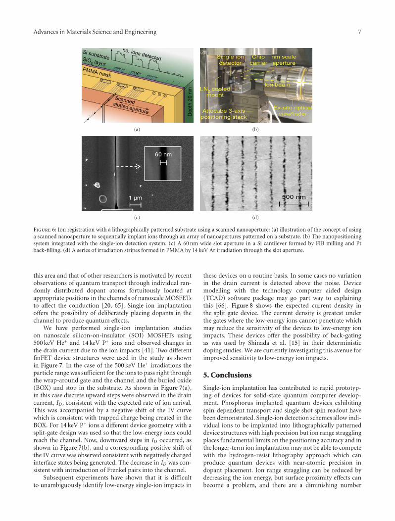
Advances in Materials Science and Engineering 7
(a) (b)
(c) (d)
Figure 6: Ion registration with a lithographically patterned substrate using a scanned nanoaperture: (a) illustration of the concept of usinga scanned nanoaperture to sequentially implant ions through an array of nanoapertures patterned on a substrate. (b) The nanopositioningsystem integrated with the single-ion detection system. (c) A 60 nm wide slot aperture in a Si cantilever formed by FIB milling and Ptback-filling. (d) A series of irradiation stripes formed in PMMA by 14 keV Ar irradiation through the slot aperture.
this area and that of other researchers is motivated by recentobservations of quantum transport through individual ran-domly distributed dopant atoms fortuitously located atappropriate positions in the channels of nanoscale MOSFETsto affect the conduction [20, 65]. Single-ion implantationoffers the possibility of deliberately placing dopants in thechannel to produce quantum effects.
We have performed single-ion implantation studieson nanoscale silicon-on-insulator (SOI) MOSFETs using500 keV He+ and 14 keV P+ ions and observed changes inthe drain current due to the ion impacts [41]. Two differentfinFET device structures were used in the study as shownin Figure 7. In the case of the 500 keV He+ irradiations theparticle range was sufficient for the ions to pass right throughthe wrap-around gate and the channel and the buried oxide(BOX) and stop in the substrate. As shown in Figure 7(a),in this case discrete upward steps were observed in the draincurrent, ID, consistent with the expected rate of ion arrival.This was accompanied by a negative shift of the IV curvewhich is consistent with trapped charge being created in theBOX. For 14 keV P+ ions a different device geometry with asplit-gate design was used so that the low-energy ions couldreach the channel. Now, downward steps in ID occurred, asshown in Figure 7(b), and a corresponding positive shift ofthe IV curve was observed consistent with negatively chargedinterface states being generated. The decrease in ID was con-sistent with introduction of Frenkel pairs into the channel.
Subsequent experiments have shown that it is difficultto unambiguously identify low-energy single-ion impacts in
these devices on a routine basis. In some cases no variationin the drain current is detected above the noise. Devicemodelling with the technology computer aided design(TCAD) software package may go part way to explainingthis [66]. Figure 8 shows the expected current density inthe split gate device. The current density is greatest underthe gates where the low-energy ions cannot penetrate whichmay reduce the sensitivity of the devices to low-energy ionimpacts. These devices offer the possibility of back-gatingas was used by Shinada et al. [15] in their deterministicdoping studies. We are currently investigating this avenue forimproved sensitivity to low-energy ion impacts.
5. Conclusions
Single-ion implantation has contributed to rapid prototyp-ing of devices for solid-state quantum computer develop-ment. Phosphorus implanted quantum devices exhibitingspin-dependent transport and single shot spin readout havebeen demonstrated. Single-ion detection schemes allow indi-vidual ions to be implanted into lithographically patterneddevice structures with high precision but ion range stragglingplaces fundamental limits on the positioning accuracy and inthe longer-term ion implantation may not be able to competewith the hydrogen-resist lithography approach which canproduce quantum devices with near-atomic precision indopant placement. Ion range straggling can be reduced bydecreasing the ion energy, but surface proximity effects canbecome a problem, and there are a diminishing number
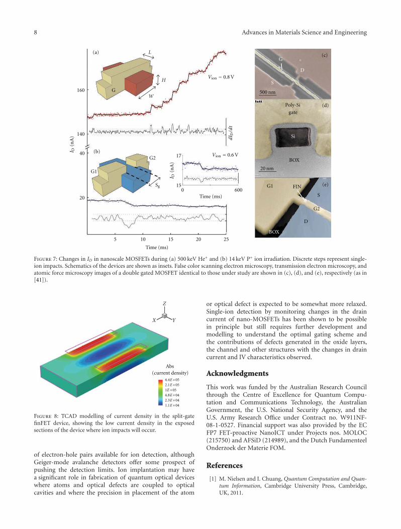
8 Advances in Materials Science and Engineering
(a)
(b)
(c)
(d)
(e)
L
H
W
Vion = 0.8 V
20
40
140
160
5 10 15 20 25
Time (ms)
Time (ms)
G
G1
G1
G2
G2
Sg
Vion = 0.6 V
0 60015
17
G
D
D
S
S
500 nm
20 nm
Poly-Si
gate
Si
BOX
BOX
FIN
I D(n
A)
I D(n
A)
dI D/dt
Figure 7: Changes in ID in nanoscale MOSFETs during (a) 500 keV He+ and (b) 14 keV P+ ion irradiation. Discrete steps represent single-ion impacts. Schematics of the devices are shown as insets. False color scanning electron microscopy, transmission electron microscopy, andatomic force microscopy images of a double gated MOSFET identical to those under study are shown in (c), (d), and (e), respectively (as in[41]).
X Y
Z
Abs(current density)
4.4E +052.1E +051E +054.8E +042.3E +041.1E +04
Figure 8: TCAD modelling of current density in the split-gatefinFET device, showing the low current density in the exposedsections of the device where ion impacts will occur.
of electron-hole pairs available for ion detection, althoughGeiger-mode avalanche detectors offer some prospect ofpushing the detection limits. Ion implantation may havea significant role in fabrication of quantum optical deviceswhere atoms and optical defects are coupled to opticalcavities and where the precision in placement of the atom
or optical defect is expected to be somewhat more relaxed.Single-ion detection by monitoring changes in the draincurrent of nano-MOSFETs has been shown to be possiblein principle but still requires further development andmodelling to understand the optimal gating scheme andthe contributions of defects generated in the oxide layers,the channel and other structures with the changes in draincurrent and IV characteristics observed.
Acknowledgments
This work was funded by the Australian Research Councilthrough the Centre of Excellence for Quantum Compu-tation and Communications Technology, the AustralianGovernment, the U.S. National Security Agency, and theU.S. Army Research Office under Contract no. W911NF-08-1-0527. Financial support was also provided by the ECFP7 FET-proactive NanoICT under Projects nos. MOLOC(215750) and AFSiD (214989), and the Dutch FundamenteelOnderzoek der Materie FOM.
References
[1] M. Nielsen and I. Chuang, Quantum Computation and Quan-tum Information, Cambridge University Press, Cambridge,UK, 2011.

Advances in Materials Science and Engineering 9
[2] A. Steane, “Quantum computing,” Reports on Progress inPhysics, vol. 61, no. 2, pp. 117–173, 1998.
[3] R. Feynman, “There’s plenty of room at the bottom,” Engineer-ing and Science, vol. 23, no. 5, pp. 22–36, 1960.
[4] R. P. Feynman, “Simulating physics with computers,” Interna-tional Journal of Theoretical Physics, vol. 21, no. 6-7, pp. 467–488, 1982.
[5] B. E. Kane, “A silicon-based nuclear spin quantum computer,”Nature, vol. 393, no. 6681, pp. 133–137, 1998.
[6] R. Vrijen, E. Yablonovitch, K. Wang et al., “Electron-spin-resonance transistors for quantum computing in silicon-germanium heterostructures,” Physical Review A, vol. 62, no.1, pp. 012306–012301, 2000.
[7] C. D. Hill, L. C. L. Hollenberg, A. G. Fowler, C. J. Wellard, A. D.Greentree, and H. S. Goan, “Global control and fast solid-statedonor electron spin quantum computing,” Physical Review B,vol. 72, no. 4, Article ID 045350, pp. 1–9, 2005.
[8] L. C. L. Hollenberg, A. S. Dzurak, C. Wellard et al., “Charge-based quantum computing using single donors in semicon-ductors,” Physical Review B, vol. 69, no. 11, Article ID 113301,pp. 1133011–1133014, 2004.
[9] B. Koiller, X. Hu, and S. Das Sarma, “Exchange in silicon-basedquantum computer architecture,” Physical Review Letters, vol.88, no. 2, Article ID 027903, pp. 279031–279034, 2002.
[10] L. C. L. Hollenberg, A. D. Greentree, A. G. Fowler, and C.J. Wellard, “Two-dimensional architectures for donor-basedquantum computing,” Physical Review B, vol. 74, no. 4, ArticleID 045311, 2006.
[11] S. J. Angus, A. J. Ferguson, A. S. Dzurak, and R. G. Clark,“Gate-defined quantum dots in intrinsic silicon,” Nano Letters,vol. 7, no. 7, pp. 2051–2055, 2007.
[12] A. Morello, C. C. Escott, H. Huebl et al., “Architecture forhigh-sensitivity single-shot readout and control of the electronspin of individual donors in silicon,” Physical Review B, vol. 80,no. 8, Article ID 081307R, 2009.
[13] K. Y. Tan, K. W. Chan, M. Mottonen et al., “Transport Spec-troscopy of single phosphorus donors in a silicon nanoscaletransistor,” Nano Letters, vol. 10, no. 1, pp. 11–15, 2010.
[14] A. Morello, J. J. Pla, F. A. Zwanenburg et al., “Single-shotreadout of an electron spin in silicon,” Nature, vol. 467, no.7316, pp. 687–691, 2010.
[15] T. Shinada, S. Okamoto, T. Kobayashi, and I. Ohdomari,“Enhancing semiconductor device performance using ordereddopant arrays,” Nature, vol. 437, no. 7062, pp. 1128–1131,2005.
[16] K. Bernstein, D. J. Frank, A. E. Gattiker et al., “High-performance CMOS variability in the 65 nm regime andbeyond,” IBM Journal of Research and Development, vol. 50,no. 4-5, pp. 433–449, 2006.
[17] M. Hori, T. Shinada, K. Taira et al., “Performance enhance-ment of semiconductor devices by control of discrete dopantdistribution,” Nanotechnology, vol. 20, no. 36, Article ID365205, 2009.
[18] T. Shinada, T. Kurosawa, H. Nakayama, Y. Zhu, M. Hori,and I. Ohdomari, “A reliable method for the counting andcontrol of single ions for single-dopant controlled devices,”Nanotechnology, vol. 19, no. 34, Article ID 345202, 2008.
[19] T. Shinada, M. Hori, K. Taira, T. Endoh, and I. Ohdomari,“Recent advance in single-ion implantation method for single-dopant devices,” in Proceedings of the 9th International Work-shop on Junction Technology, IWJT 2009, pp. 96–99, Kyoto,Japan, June 2009.
[20] M. Pierre, R. Wacquez, X. Jehl, M. Sanquer, M. Vinet, andO. Cueto, “Single-donor ionization energies in a nanoscale
CMOS channel,” Nature Nanotechnology, vol. 5, no. 2, pp. 133–137, 2010.
[21] E. L. Waller and T. Shinada, Eds., “ITRS ERM workshop series:deterministic doping,” Berkeley, Calif, USA, 2010 http://www.src.org/calendar/e004100/.
[22] J. R. Rabeau, P. Reichart, G. Tamanyan et al., “Implantationof labelled single nitrogen vacancy centers in diamond using15N,” Applied Physics Letters, vol. 88, no. 2, Article ID 023113,pp. 1–3, 2006.
[23] G. D. Fuchs, V. V. Dobrovitski, R. Hanson et al., “Excited-statespectroscopy using single Spin manipulation in diamond,”Physical Review Letters, vol. 101, no. 11, Article ID 117601,2008.
[24] S. Pezzagna, D. Wildanger, P. Mazarov et al., “Nanoscale engi-neering and optical addressing of single spins in diamond,”Small, vol. 6, no. 19, pp. 2117–2121, 2010.
[25] D. M. Toyli, C. D. Weis, G. D. Fuchs, T. Schenkel, and D. D.Awschalom, “Chip-scale nanofabrication of single spins andspin arrays in diamond,” Nano Letters, vol. 10, no. 8, pp. 3168–3172, 2010.
[26] P. Spinicelli, A. Dreau, L. Rondin et al., “Engineered arraysof nitrogen-vacancy color centers in diamond based onimplantation of cn? Molecules through nanoapertures,” NewJournal of Physics, vol. 13, Article ID 025014, 2011.
[27] H. Huebl, C. D. Nugroho, A. Morello et al., “Electron tunnelrates in a donor-silicon single electron transistor hybrid,”Physical Review B, vol. 81, no. 23, Article ID 235318, 2010.
[28] T. Schenkel, A. Persaud, S. J. Park et al., “Solid statequantum computer development in silicon with single ionimplantation,” Journal of Applied Physics, vol. 94, no. 11, pp.7017–7024, 2003.
[29] V. Millar, C. I. Pakes, S. Prawer, B. Rout, and D. N. Jamieson,“Thin film resists for registration of single-ion impacts,”Nanotechnology, vol. 16, no. 6, pp. 823–826, 2005.
[30] D. N. Jamieson, C. Yang, T. Hopf et al., “Controlled shallowsingle-ion implantation in silicon using an active substratefor sub- 20-keV ions,” Applied Physics Letters, vol. 86, no. 20,Article ID 202101, pp. 1–3, 2005.
[31] J. F. Ziegler, J. P. Biersack, and U. Littmark, SRIM The Stoppingand Range of Ions in Solids, Pergamon, New York, NY, USA,1985.
[32] T. Hopf, Single ion implantation for construction of a quantumcomputer, Ph.D. thesis, University of Melbourne, 2007.
[33] T. Hopf, C. Yang, S. M. Hearne et al., “Low-noise detectionsystem for the counted implantation of single ions in silicon,”IEEE Transactions on Nuclear Science, vol. 55, no. 2, Article ID4484234, pp. 812–816, 2008.
[34] T. Schenkel, J. A. Liddle, A. Persaud et al., “Electrical activationand electron spin coherence of ultralow dose antimonyimplants in silicon,” Applied Physics Letters, vol. 88, no. 11,Article ID 112101, 2006.
[35] T. Schenkel, C. C. Lo, C. D. Weis, A. Schuh, A. Persaud, and J.Bokor, “Critical issues in the formation of quantum computertest structures by ion implantation,” Nuclear Instruments andMethods in Physics Research, Section B, vol. 267, no. 16, pp.2563–2566, 2009.
[36] C. C. Lo, J. Bokor, T. Schenkel, A. M. Tyryshkin, and S.A.Lyon, “Spin-dependent scattering off neutral antimony donorsin 28Si field-effect transistors,” Applied Physics Letters, vol. 91,Article ID 242106, 3 pages, 2007.
[37] J. C. McCallum, M. L. Dunn, and E. Gauja, “Ion implantationthrough thin silicon dioxide layers for Si-based solid-statequantum computer device development,” MRS Proceedings,vol. 1074, Article ID 1074-I12-05, 2008.

10 Advances in Materials Science and Engineering
[38] J. A. Van Donkelaar, A. D. Greentree, A. D. C. Alves, L. M.Jong, L. C. L. Hollenberg, and D. N. Jamieson, “Top-downpathways to devices with few and single atoms placed to highprecision,” New Journal of Physics, vol. 12, Article ID 065016,p. 1367, 2010.
[39] H. O. Funsten, S. M. Ritzau, R. W. Harper, and R. Korde,“Response of 100% internal carrier collection efficiency siliconphotodiodes to low-energy ions,” IEEE Transactions on NuclearScience, vol. 48, no. 6, pp. 1785–1789, 2001.
[40] T. Hopf, C. Yang, S. E. Andresen, and D. N. Jamieson, “Theresponse of silicon detectors to low-energy ion implantation,”Journal of Physics Condensed Matter, vol. 20, no. 41, Article ID415205, 2008.
[41] B. C. Johnson, G. C. Tettamanzi, A. D. C. Alves et al., “Draincurrent modulation in a nanoscale field-effect-transistorchannel by single dopant implantation,” Applied PhysicsLetters, vol. 96, no. 26, Article ID 264102, 2010.
[42] A. D. Greentree, J. H. Cole, A. R. Hamilton, and L. C. L.Hollenberg, “Coherent electronic transfer in quantum dotsystems using adiabatic passage,” Physical Review B, vol. 70,no. 23, Article ID 235317, pp. 1–6, 2004.
[43] R. Rahman, R. P. Muller, J. E. Levy et al., “Coherent electrontransport by adiabatic passage in an imperfect donor chain,”Physical Review B, vol. 82, no. 15, Article ID 155315, 2010.
[44] Y. P. Song and B. Golding, “Manipulation and decoherence ofacceptor states in silicon,” EPL, vol. 95, no. 4, Article ID 47004,2011.
[45] A. M. Tyryshkin, S. A. Lyon, T. Schenkel et al., “Electron spincoherence in Si,” Physica E, vol. 35, no. 2, pp. 257–263, 2006.
[46] M. J. Calderon, B. Koiller, and S. D. Sarma, “External fieldcontrol of donor electron exchange at the Si/Si O2 interface,”Physical Review B, vol. 75, no. 12, Article ID 125311, 2007.
[47] H. O. Funsten, S. M. Ritzau, R. W. Harper, and R. Korde,“Fundamental limits to detection of low-energy ions usingsilicon solid-state detectors,” Applied Physics Letters, vol. 84,no. 18, pp. 3552–3554, 2004.
[48] H. O. Funsten, S. M. Ritzau, R. W. Harper, J. E. Borovsky, andR. E. Johnson, “Energy loss by keV ions in silicon,” PhysicalReview Letters, vol. 92, no. 21, Article ID 213201, 2004.
[49] A. Akkerman and J. Barak, “New partition factor calculationsfor evaluating the damage of low energy ions in silicon,” IEEETransactions on Nuclear Science, vol. 53, no. 6, pp. 3667–3674,2006.
[50] A. Akkerman and J. Barak, “Partitioning to elastic and inelasticprocesses of the energy deposited by low energy ions insilicon detectors,” Nuclear Instruments and Methods in PhysicsResearch, Section B, vol. 260, no. 2, pp. 529–536, 2007.
[51] P. A. Ekstrom, “Triggered-avalanche detection of optical pho-tons,” Journal of Applied Physics, vol. 52, no. 11, pp. 6974–6979,1981.
[52] J. A. Seamons, E. Bielejec, M. S. Carroll, and K. D. Childs,“Room temperature single ion detection with Geiger modeavalanche diode detectors,” Applied Physics Letters, vol. 93, no.4, Article ID 043124, 2008.
[53] E. Bielejec, J. A. Seamons, and M. S. Carroll, “Single ionimplantation for single donor devices using Geiger modedetectors,” Nanotechnology, vol. 21, no. 8, Article ID 085201,2010.
[54] J. Meijer, T. Vogel, B. Burchard et al., “Concept of deterministicsingle ion doping with sub-nm spatial resolution,” AppliedPhysics A, vol. 83, no. 2, pp. 321–327, 2006.
[55] J. L. Hanssen, S. B. Hill, J. Orloff, and J. J. McClelland,“Magneto-optical-trap-based, high brightness ion source for
Use as a nanoscale probe,” Nano Letters, vol. 8, no. 9, pp. 2844–2850, 2008.
[56] W. Schnitzler, N. M. Linke, R. Fickler, J. Meijer, F. Schmidt-Kaler, and K. Singer, “Deterministic ultracold ion sourcetargeting the Heisenberg limit,” Physical Review Letters, vol.102, no. 7, Article ID 070501, 2009.
[57] T. Schenkel, V. Radmilovic, E. A. Stach, S. J. Park, andA. Persaud, “Formation of a few nanometer wide holes inmembranes with a dual beam focused ion beam system,”Journal of Vacuum Science and Technology B, vol. 21, no. 6, pp.2720–2723, 2003.
[58] A. Persaud, K. Ivanova, Y. Sarov et al., “Micromachinedpiezoresistive proximal probe with integrated bimorph actu-ator for aligned single ion implantation,” Journal of VacuumScience and Technology B, vol. 24, no. 6, pp. 3148–3151, 2006.
[59] Systems AG Attocube, “Koniginstrasse 11a RGB 80539,”Munchen, Germany.
[60] S. R. Schofield, N. J. Curson, M. Y. Simmons et al., “Atomicallyprecise placement of single dopants in Si,” Physical ReviewLetters, vol. 91, no. 13, pp. 1361041–1361044, 2003.
[61] M. Fuechsle, S. Mahapatra, F. A. Zwanenburg, M. Friesen,M. A. Eriksson, and M. Y. Simmons, “Spectroscopy of few-electron single-crystal silicon quantum dots,” Nature Nan-otechnology, vol. 5, no. 7, pp. 502–505, 2010.
[62] E. Peter, P. Senellart, D. Martrou et al., “Exciton-photonstrong-coupling regime for a single quantum dot embeddedin a microcavity,” Physical Review Letters, vol. 95, no. 6, ArticleID 067401, pp. 1–4, 2005.
[63] A. Batra, C. D. Weis, J. Reijonen et al., “Detection of lowenergy single ion impacts in micron scale transistors at roomtemperature,” Applied Physics Letters, vol. 91, no. 19, Article ID193502, 2007.
[64] C. D. Weis, A. Schuh, A. Batra et al., “Single atom dopingfor quantum device development in diamond and silicon,”Journal of Vacuum Science and Technology B, vol. 26, no. 6, pp.2596–2600, 2008.
[65] G. P. Lansbergen, R. Rahman, C. J. Wellard et al., “Gate-induced quantum-confinement transition of a single dopantatom in a silicon FinFET,” Nature Physics, vol. 4, no. 8, pp.656–661, 2008.
[66] “Synopsys, Inc., 700 East Middlefield Road, Mountain,” View,CA 94043.

Hindawi Publishing CorporationAdvances in Materials Science and EngineeringVolume 2012, Article ID 610150, 9 pagesdoi:10.1155/2012/610150
Research Article
Purity of Ion Beams: Analysis and Simulation of Mass Spectraand Mass Interferences in Ion Implantation
Volker Haublein,1 Heiner Ryssel,1, 2 and Lothar Frey1, 2
1 Fraunhofer Institut fur Integrierte Systeme und Bauelementetechnologie, Schottkystrasse 10, 91058 Erlangen, Germany2 Lehrstuhl fur Elektronische Bauelemente, Universitat Erlangen, Cauerstrasse 6, 91058 Erlangen, Germany
Correspondence should be addressed to Volker Haublein, [email protected]
Received 1 July 2011; Accepted 5 August 2011
Academic Editor: Joseph Gyulai
Copyright © 2012 Volker Haublein et al. This is an open access article distributed under the Creative Commons AttributionLicense, which permits unrestricted use, distribution, and reproduction in any medium, provided the original work is properlycited.
This paper shows that charge exchange events and dissociation reactions of ions may impact the purity of the ion beam in ionimplantation, leading to contamination of the implanted target. Physical relations are derived that explain why unwanted ions aretransported in the ion beam despite of a magnetic mass separation. Based on those relations, the simulation tool ENCOTION(ENergetic COntamination simulaTION) has been developed. ENCOTION is a very powerful tool for the simulation of transportmechanisms of ions through a magnet analyzer and for the simulation of mass spectra, as will be demonstrated in this paper.
1. Introduction
The modification of materials by ion implantation offersmajor advantages, such as high dose accuracy, excellent re-producibility, or low process temperatures. Due to its massseparation, ion implantation is considered to be an extremelyclean process step. Many applications, such as CCDs orbipolar devices, strongly depend on the purity of the ionbeam [1]. The coimplantation of other contaminating ionspecies might lead to serious consequences:
(i) dose errors, especially when the amount of contami-nating ions is significantly high;
(ii) differences in the defect formation, for example,when the contaminating ion species is much heavierthan the desired ion species;
(iii) impairment or complete malfunction of the irradi-ated device, for example, in bipolar devices when thecontaminating ion species forms deep recombinationcenters;
(iv) unreproducible implantation results as the composi-tion of the ion beam might change with source para-meters (especially temperature) as well as with thehistory of the ion source.
Basically, mass interferences occur when the masses of dif-ferent ion species are so close that the analyzer magnetcannot separate them. For example, As may be implantedtogether with Ge, when As is directly implanted after a Gepreamorphization implant [2]. A key parameter for massseparation, therefore, is the mass resolution M/ΔM whichcan have great impact on the ion beam composition [3]. Thehigher the mass resolution is, the lower the risk for contam-ination is. Modern ion implanters have mass resolutions inthe range of about 15 to 90, whereas for the purpose of a highion beam purity, a value of more than 100 is recommended[3].
Since mass separation is accomplished by magneticfields, it is well known that the ions are not separated bytheir mass, but rather by the mass to charge state ratio. Aprominent example for contamination from device manu-facturing is the coimplantation of doubly charged Mo duringBF2 implantation where the mass to charge state ratio is 49in both cases [4, 5]. The simultaneous implantation of un-wanted ions with the same mass to charge ratio as the desiredion species might appear to be a manageable contaminationrisk, but it is only a special case. When ions undergo a chargeexchange or dissociate between the ion source and the anal-yzer magnet, surprising contamination issues may arise [6–8]. This paper illustrates by means of mass spectrum analysis

2 Advances in Materials Science and Engineering
(which is not only essential in order to check which elementsare present in the ion source) that charge exchange eventsand dissociation processes between the ion source and theanalyzer magnet of an implanter are fairly common. In thisregard, an important result of this paper is that those re-actions generally produce two peaks in a mass spectrum,whereof one not only depends on the mass and charge statesof the considered ions, but also on the extraction and sup-pression voltages of the implanter. Simulations with the pre-sented tool ENCOTION reveal that those charge exchangeand dissociation processes basically allow for a large varietyof potential transport mechanisms for practically all ele-ments.
2. Apparent Mass Concept
The derivation of the apparent mass models is based on theequation of Lorentz force and centrifugal force:
Bqanev = manv2
r, (1)
where B is the magnetic flux density, r the radius of the mag-net, e the elementary charge, v the velocity of the analyzed
ion, and man and qan are mass and charge state of the ion inthe analyzer.
Three sections have to be distinguished in the beamlinefrom the ion source to the analyzer magnet (see Figure 1):
(1) [Src-Ex] section between ion source and extractionelectrode;
(2) [Ex-Gnd] section between extraction and groundelectrode;
(3) [Gnd-An] section between ground electrode andanalyzer.
When a mass or charge exchange event occurs withinsection [Src-Ex] or section [Ex-Gnd], the final velocity of anion in the magnet depends on the exact position in those sec-tions. Therefore, the variables zex and zsp describe the relativeposition of the charge or mass changing event in section [Src-Ex] and section [Ex-Gnd], respectively, and take values from0 to 1 (see Figure 1). Under the assumptions that in any of thethree sections no more than one charge or mass changingevent takes place and that the impact of the event itself on thevelocity is negligible, the velocity of the ion in the magnet cal-culates as follows:
v = √2e ·√√√√( qsc
msczex +
qex
mex(1− zex)
)(Vex + Vsp
)−(qex
mexzsp +
qsp
msp
(1− zsp
))Vsp, (2)
where msc and qsc are mass and charge state of an ion leavingthe ion source, mex and qex are mass and charge state at theextraction electrode, and msp and qsp are mass and chargestate at the ground electrode. Inserting (2) in (1), a generalexpression for the apparent mass can be derived:
mapp = m2an
q2an
[(qsc
msczex +
qex
mex(1− zex)
)(1 +
Vsp
Vex
)
−(qex
mexzsp +
qsp
msp
(1− zsp
))Vsp
Vex
].
(3)
According to (3), the apparent mass depends not onlyon the mass and charge states of the ions, but also on theratio of suppression and extraction voltage. Because of thevariables zex and zsp, the apparent mass is not limited todiscrete values but can take values from a continuous range.Equation (3), therefore, is appropriate to describe tails ofpeaks in a mass spectrum, such as the Al tail in Figure 4 inthe next section or to model contamination problems wherethe charge exchange occurs in section [Src-Ex] [8].
In order to describe and simulate peaks of a mass spec-trum, (3) can be simplified by applying the following assum-ptions:
(i) on its way from the ion source to the analyzer magnet,an ion undergoes no more than one change in massor charge state;
(ii) the charge or mass change events occur either at thesuppression or the ground electrode (zex = zsp = 1)or between ground electrode and magnet.
According to those assumptions, two expressions for theapparent mass can be derived:
(1) charge exchange or dissociation at extraction elec-trode (man = msp, msc = mex, qan = qsp, and qsc =qex):
mapp = m2an
q2an
[qsc
msc+Vsp
Vex·(qsc
msc− qan
man
)], (4)
(2) charge exchange or dissociation at ground electrodeor beyond (msc = mex = msp and qsc = qex = qsp):
mapp = m2an
q2an
qsc
msc. (5)
Both expressions for the apparent mass, (4) and (5), yielddiscrete mass values. The particularity of (4) is the depen-dence of the apparent mass on the ratio of the extraction andsuppression voltages, while the apparent mass according to(5) only depends on masses and charge states of the consid-ered ions. Equation (5) is well known and has been widelyused to explain contamination issues in ion implantation[9, 10]. Both equations are the fundament for understandinga variety of peaks in mass spectra.

Advances in Materials Science and Engineering 3
e−
e−
e−
e−
e−
e−
e−
e−e−
e−
Extraction
electrode
Ground
electrode
Vex + Vsp Vsp
1
[Src-Ex] [Ex-Gnd] [Gnd-An]
Ion beam
Ion source
Analyzer
magnet
0
0
Zex
Zsp 1
Figure 1: Layout of the beamline of an implanter from ion source to analyzer magnet. The beamline is divided into the three sections [Src-Ex], [Ex-Gnd], and [Gnd-An]. The ion beam generates secondary electrons which are accelerated in the sections [Src-Ex] and [Ex-Gnd].
W+++ W++
W++
W+
W+
WP+
WF+P +
4
AsP+
Mo+
Extraction voltage: 20.2 kV
Source gas: PH3
100
101
10− 1
10− 2
10− 3
90 100 110 120 130 140 150 160 170 180 190 200
Mass (u)
Bea
mcu
rren
t(μ
A)
Figure 2: Section of a PH3 mass spectrum.
3. Analysis of Mass Spectra
A set of mass spectra with different source feed materials,such as AsH3, PH3, N2, BF3, and Al were recorded and anal-yzed. The mass spectra were recorded on a Varian 350 D im-planter with a mass resolution M/ΔM between 100 and 120.The Freeman ion source consists of a molybdenum arc cham-ber and a tungsten filament which is insulated by aluminaceramics. The recording of the spectra and the control of theanalyzer magnet were accomplished by a self-programmedLabView software. It is of great importance that the ion cur-rent can be recorded over several orders of magnitude. In thefollowing, selected sections of the mass spectra are depictedin order to demonstrate the occurrence of charge exchangeand dissociation reactions.
Figure 2 shows a mass spectrum from 85 u to 220 u for anion source being operated with PH3. Tungsten with its fiveisotopes produces a very characteristic arrangement of W+
As+++ As++
As +3 As ++
3
P +2
AsP++
Mass (u)
Bea
mcu
rren
t(μ
A)
100
10− 1
10− 2
(after extraction)
Extraction voltages:
30.1 kV25.1 kV20.2 kV
Source gas: AsH3
51 52 53 54 55 56 57 58 59 60 61 62 63
As+++ As++
W+++
(at extractionelectrode)
Figure 3: Section of an AsH3 mass spectrum.
peaks between 180 u and 186 u. In Figure 2, this arrangementof peaks also shows up at four other positions. The peaksfrom 90 u to 93 u and from 199 u to 205 u represent the sig-nals of W++ and WF+ ions, respectively. The remaining Wpeaks are caused by charge exchange and dissociation re-actions. The peaks from 135 u to 139 u and 150 u to 156 u, arethe results of the charge exchange reaction W+++ → W++
and the dissociation process WP+ → W+, respectively.Figure 3 shows three mass spectra from 51 u to 63 u, each
recorded at a different extraction voltage, and the source feedgas was AsH3. The signal at mass 56.2 u is attributed to Asand can be caused in agreement with (5) by two differentcharge exchange mechanisms:
(i) As+++ → As++ (at or beyond ground electrode),
(ii) As3+ → As3
++ (at or beyond ground electrode).
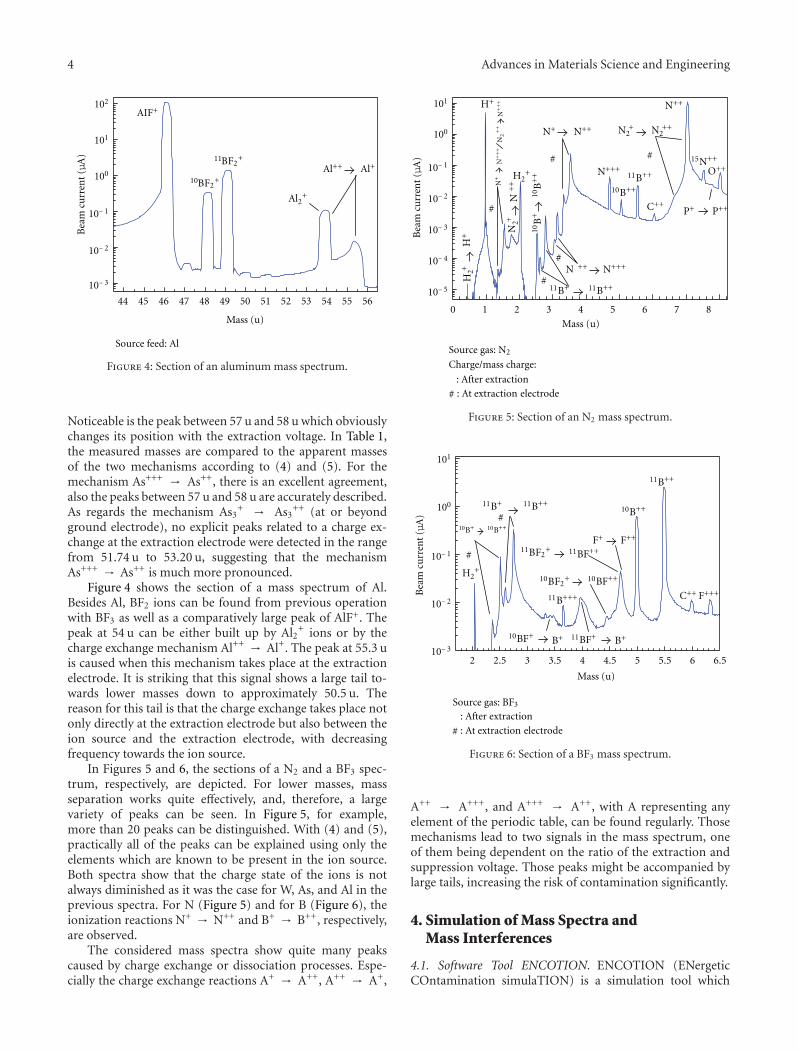
4 Advances in Materials Science and Engineering
11
10
Al++ Al+
Al +2
100
102
101
10− 1
10− 2
10− 3
44 45 46 47 48 49 50 51 52 53 54 55 56
Mass (u)
Bea
mcu
rren
t(μ
A)
Source feed: Al
AIF+
BF2+
BF2+
Figure 4: Section of an aluminum mass spectrum.
Noticeable is the peak between 57 u and 58 u which obviouslychanges its position with the extraction voltage. In Table 1,the measured masses are compared to the apparent massesof the two mechanisms according to (4) and (5). For themechanism As+++ → As++, there is an excellent agreement,also the peaks between 57 u and 58 u are accurately described.As regards the mechanism As3
+ → As3++ (at or beyond
ground electrode), no explicit peaks related to a charge ex-change at the extraction electrode were detected in the rangefrom 51.74 u to 53.20 u, suggesting that the mechanismAs+++ → As++ is much more pronounced.
Figure 4 shows the section of a mass spectrum of Al.Besides Al, BF2 ions can be found from previous operationwith BF3 as well as a comparatively large peak of AlF+. Thepeak at 54 u can be either built up by Al2
+ ions or by thecharge exchange mechanism Al++ → Al+. The peak at 55.3 uis caused when this mechanism takes place at the extractionelectrode. It is striking that this signal shows a large tail to-wards lower masses down to approximately 50.5 u. Thereason for this tail is that the charge exchange takes place notonly directly at the extraction electrode but also between theion source and the extraction electrode, with decreasingfrequency towards the ion source.
In Figures 5 and 6, the sections of a N2 and a BF3 spec-trum, respectively, are depicted. For lower masses, massseparation works quite effectively, and, therefore, a largevariety of peaks can be seen. In Figure 5, for example,more than 20 peaks can be distinguished. With (4) and (5),practically all of the peaks can be explained using only theelements which are known to be present in the ion source.Both spectra show that the charge state of the ions is notalways diminished as it was the case for W, As, and Al in theprevious spectra. For N (Figure 5) and for B (Figure 6), theionization reactions N+ → N++ and B+ → B++, respectively,are observed.
The considered mass spectra show quite many peakscaused by charge exchange or dissociation processes. Espe-cially the charge exchange reactions A+ → A++, A++ → A+,
N+++
N+++
N+
N+ 2
N +2 N ++
2N++
N+
+
N ++
H+
H+
H +2
H+ 2
10B
+
10B++
10B
++
11B+
11B++
11B++
C++P++P+
15N++
O++
Charge/mass charge:
: After extraction
: At electrode
0 1 2 3 4 5 6 7 8
100
101
10− 1
10− 2
10− 3
10− 4
10− 5
Source gas: N2
Mass (u)
Bea
mcu
rren
t(μ
A)
N++
N+
++
N+
++
N+
+2
N+
#
#
# #
#
# extraction
Figure 5: Section of an N2 mass spectrum.
11B++
11B++11B+10B++
10B+
11BF++
11BF+
11
10BF++10
10BF+
11B+++
F++F+
F+++
H +2
B+ B+
Source gas: BF3
2 2.5 3 3.5 4 4.5 5 5.5 6 6.5
Mass (u)
Bea
mcu
rren
t(μ
A)
100
101
10− 1
10− 2
10− 3
: After extraction
C++
10B++
#
#
BF2+
BF2+
: At electrode# extraction
Figure 6: Section of a BF3 mass spectrum.
A++ → A+++, and A+++ → A++, with A representing anyelement of the periodic table, can be found regularly. Thosemechanisms lead to two signals in the mass spectrum, oneof them being dependent on the ratio of the extraction andsuppression voltage. Those peaks might be accompanied bylarge tails, increasing the risk of contamination significantly.
4. Simulation of Mass Spectra andMass Interferences
4.1. Software Tool ENCOTION. ENCOTION (ENergeticCOntamination simulaTION) is a simulation tool which
Advances in Materials Science and Engineering 5
Table 1: Comparison of As peaks from Figure 3 with calculated apparent masses. Spectrum (a) charge exchange after extraction, spectrumand (b) charge exchange at the extraction electrode Vsp = 1.6 kV.
Mechanism Vex (kV)mapp (u)
Spectrum (a) Equation (5) Spectrum (b) Equation (4)
As+++ → As++
20.2 56.21 56.19 57.79 57.68
25.1 56.20 56.19 57.41 57.39
30.1 56.20 56.19 57.17 57.19
As3+ → As3
++20.2 56.21 56.19 n. d. 51.74
25.1 56.20 56.19 n. d. 52.61
30.1 56.20 56.19 n. d. 53.20
was originally developed in order to check the potential ofany element of the periodic table to contaminate the targetduring the ion implantation process [11]. It enables the userto simulate expeditiously transport mechanisms of contam-inants through the analyzer magnet, taking charge exchangereactions and dissociation of molecular ions into account.ENCOTION contains a database featuring the complete per-iodic table of elements. Names and symbols of the elementswith atomic numbers greater than 100 were chosen accordingto the recommendations of the International Union of Pureand Applied Chemistry (IUPAC) [12]. The database containsthe masses and abundances of all natural isotopes, and thevalues were taken from IUPAC tables [13].
Since the first version of ENCOTION was released [14],numerous improvements were made and extensions wereadded. ENCOTION now considers changes in mass andcharge state at the extraction electrode according to (4).Figure 7 shows the parameter dialog where the main sett-ings for a simulation are made. Essential for a simulation arethe definition of the apparent mass (which is preferably doneby specifying the implanted ion species in order to considerdecimals of the apparent mass) and the definition of the con-taminating element. Additionally, assisting elements can bespecified which might form a molecule with the contaminat-ing elements but which are not necessarily implanted. Forsimulating changes in mass or charge state at the extractionelectrode, the extraction and suppression voltage have to beprovided. The extraction and a postacceleration voltage areneeded to calculate the effective energy of the coimplantedcontaminating element. Other parameters, such as mass re-solution, maximum charge state, or maximum number ofcontaminants in a molecule, may be used to limit or to ex-tend the solution space. In Figure 8, a result window withsimulated transport mechanisms is depicted. For each trans-port mechanism, the extracted ion with charge state as wellas the analyzed ion with charge state are listed. In addition,the effective energies of the contaminating element with andwithout an acceleration after mass separation are provided.Finally, the apparent mass and the difference to the implan-ted mass are listed. All columns of the result window can besorted in descending or ascending order.
A major extension is the implementation of two graph-ical modules for simulating mass spectra. The first modulesimulates the spectrum peaks of two interfering ion specieseither by Gaussian curves or by consideration of geometric
parameters, such as the magnet radius, the width of the beamslit, and the standard deviation of the ion beam. The latter isespecially useful when the width of the mass resolving slit islarger than the deviation of the ion beam. The peaks can beplotted both linearly and logarithmically. Figure 9 shows anexample of a mass spectrum of Ge interfering with W.
The second module simulates mass spectra with up tofive elements, taking into account multiply charged ions andthe formation of molecular ions. In Figure 10, a window withsimulated mass spectra from 0 to 200 u is shown. The peaksare formed only by the elements B, O, F, Mo, and W underconsideration of multiply charged ions and the formation ofmolecular ions. ENCOTION allows for the comparison oftwo spectra. The total of the (red and blue) peaks describesthe spectrum spanned by all five elements. The red peakswere simulated with Mo being removed, that is, the remain-ing blue peaks are caused by ions containing Mo. The com-bination of the simulation of transport mechanisms togetherwith the graphical simulation of mass spectra makes ENCO-TION an optimum tool for identifying peaks in measuredmass spectra.
4.2. Simulation of Mass Spectra. To identify unknown peaksin mass spectra, the simulation of transport mechanisms canbe complemented by the simulation of graphical mass spec-tra. This is especially promising when elements with morethan one isotope are involved. In Figure 11, a BF3 massspectrum from 108 u to 120 u is shown. None of the peaksfeatures tails or shoulders which might indicate that they arebuilt by superpositions of different peaks. In fact, the sim-ulation with ENCOTION reveals that the peaks are causedby a superposition of 41.7% MoO+ and 58.3% MoF+ ions. Incase that the magnet analyzer would be set to mass 114 u, theion beam would consist of 26% 98Mo, 24% 95Mo, 26% 16O,and 24% 19F.
Another spectrum simulation is shown in Figure 12. Theion source was initially operated with AsH3 for As implanta-tion, when subsequently the source feed gas was switched toN2. At mass 75 u, the As+ peak is visible. In the mass regionbetween 69 u and 74 u, the measurement indicates a fewmore peaks. It is striking that the distance of the peaks bet-ween 70 u and 72 u is not 1 u but 0.75 u. The mass spectrumsimulation with ENCOTION identifies those peaks to becaused by the charge exchange reaction Mo+++ → Mo++. In

6 Advances in Materials Science and Engineering
Figure 7: Parameter dialog of ENCOTION. In this dialog, the main parameters, such as the implanted ion species and the contaminatingelements, are specified.
Figure 8: Result window of ENCOTION. The simulated transport mechanisms are organized in nine sortable columns, containing the ex-tracted and analyzed ions, the effective energies of the contaminating element with and without postacceleration, the simulated apparentmass, and the mass difference to the apparent mass of the implanted ion. In this example, the simulated transport mechanisms of Al during11B+ implantation are listed, sorted by effective energy in ascending order.
this case, the peak caused by 100Mo overlaps exactly with thepeak of As, that is, the As beam is contaminated with 100Mo.
4.3. Identification of Contamination Mechanisms. In manycases, simulations with ENCOTION show surprisingly largenumbers of possibilities of how a peak in a mass spectrummight be caused or how an unwanted element might con-
tribute to contamination of the implanted target. This makesit sometimes difficult to unambiguously assign the cause of apeak in a mass spectrum, especially when only elements withone isotope come into consideration. For ion implantation,the peak of the desired ion species is aimed to be tuned aslarge as possible, making it in most cases impossible to ratewhether this peak conceals peaks of other ion species or

Advances in Materials Science and Engineering 7
Figure 9: Mass spectrum module 1 of ENCOTION. The simulated spectra show an interference between Ge and W ions.
Figure 10: Mass spectrum module 2 of ENCOTION. The simulated mass spectra from 0 to 200 u show peaks simulated by multiply chargedand molecular ions of the elements B, O, F, Mo, and W. All peaks that are caused by ions containing Mo are plotted in blue.
not. In those cases, the simulations should be supported bySIMS measurements. SIMS profiles not only describe the im-planted amount of considered elements, they also allow toconclude on the effective implantation energy. With the lat-ter, the simulated transport mechanisms can be rated.
Figure 13 shows SIMS profiles of Al which were measuredon two silicon wafers that were implanted with 11B+, onewafer with 70 keV, the other with 140 keV. The 70 keV im-plant was realized with an extraction voltage of 70 kV, and the140 keV implant had an additional acceleration after massseparation at a voltage of 70 kV. Profile simulations with theMonte Carlo software SRIM [15] indicate that the Al was im-planted at energies of 18 keV and 74 keV, respectively.In Table 2, the two potential transport mechanisms withthe lowest effective energies are listed (cp. simulationsin Figure 8). The energy of the mechanism Al2O3
+ →Al2O3
+++ agrees very well with the energies extracted by the
Table 2: Simulated transport mechanisms for Al to be coimplantedduring a 11B+-implantation. The energy E1 results from an extrac-tion voltage of 70 kV + 70 kV, and the energy E2 from an extractionvoltage and an additional acceleration voltage after mass separationof 70 kV each (cf. Figure 8).
Mechanism mapp (u) E1 (keV) E2 (keV)
Al2O3+ → Al2O3
+++ 11.329 18.5 74.1
AlF2+ → Al+ 11.204 29.1 99.1
SRIM profiles. Since alumina ceramics are present in theion source, this mechanism appears feasible. The tails of theSIMS profiles, however, suggest that also other mechanismssuch as the dissociation process AlF2
+ → Al+ mightcontribute to the contamination.
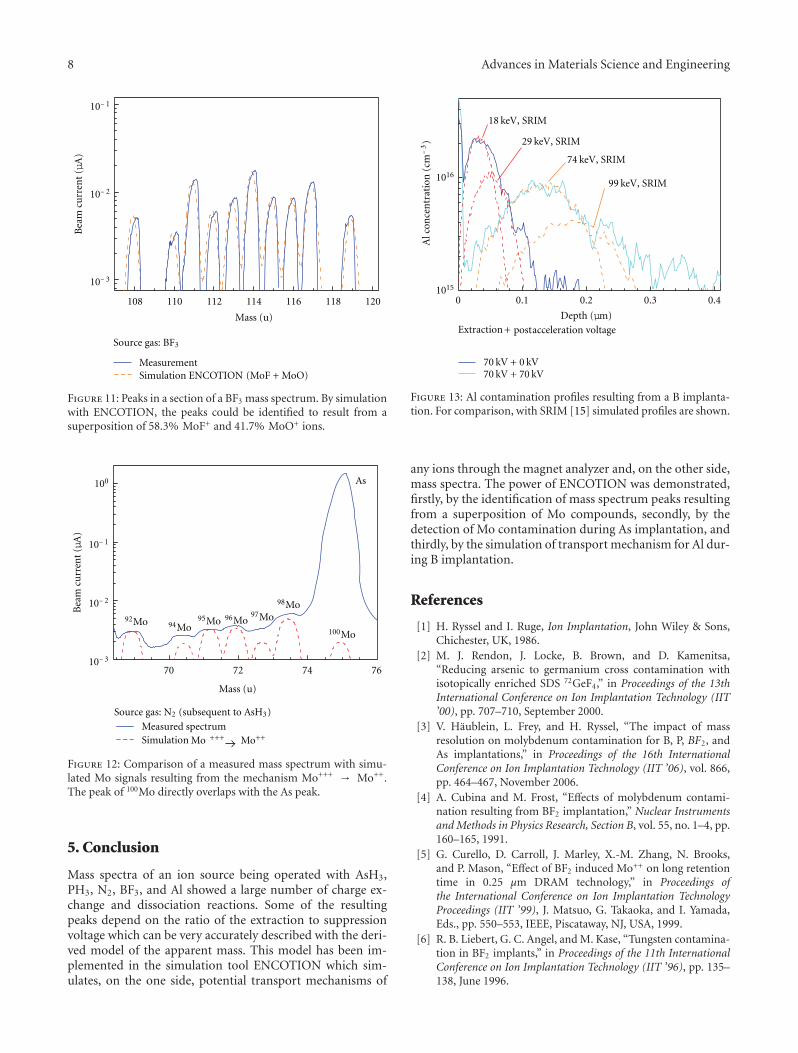
8 Advances in Materials Science and Engineering
Source gas: BF3
MeasurementSimulation ENCOTION (MoF + MoO)
108 110 112 114 116 118 120
10− 1
10− 2
10− 3
Mass (u)
Bea
mcu
rren
t(μ
A)
Figure 11: Peaks in a section of a BF3 mass spectrum. By simulationwith ENCOTION, the peaks could be identified to result from asuperposition of 58.3% MoF+ and 41.7% MoO+ ions.
94Mo92Mo 95Mo 96Mo
97Mo
98Mo
100Mo
100
10− 1
10− 2
Mass (u)
Bea
mcu
rren
t(μ
A)
70 72 74 76
Measured spectrum
Source gas: N2 (subsequent to AsH3)
As
10− 3
Mo++Mo +++Simulation
Figure 12: Comparison of a measured mass spectrum with simu-lated Mo signals resulting from the mechanism Mo+++ → Mo++.The peak of 100Mo directly overlaps with the As peak.
5. Conclusion
Mass spectra of an ion source being operated with AsH3,PH3, N2, BF3, and Al showed a large number of charge ex-change and dissociation reactions. Some of the resultingpeaks depend on the ratio of the extraction to suppressionvoltage which can be very accurately described with the deri-ved model of the apparent mass. This model has been im-plemented in the simulation tool ENCOTION which sim-ulates, on the one side, potential transport mechanisms of
18 keV, SRIM
1015
74 keV, SRIM
1016
29 keV, SRIM
99 keV, SRIM
Alc
once
ntr
atio
n(c
m−
3)
Extraction + postacceleration voltage
70 kV + 0 kV70 kV + 70 kV
0 0.1 0.2 0.3 0.4
Depth (μm)
Figure 13: Al contamination profiles resulting from a B implanta-tion. For comparison, with SRIM [15] simulated profiles are shown.
any ions through the magnet analyzer and, on the other side,mass spectra. The power of ENCOTION was demonstrated,firstly, by the identification of mass spectrum peaks resultingfrom a superposition of Mo compounds, secondly, by thedetection of Mo contamination during As implantation, andthirdly, by the simulation of transport mechanism for Al dur-ing B implantation.
References
[1] H. Ryssel and I. Ruge, Ion Implantation, John Wiley & Sons,Chichester, UK, 1986.
[2] M. J. Rendon, J. Locke, B. Brown, and D. Kamenitsa,“Reducing arsenic to germanium cross contamination withisotopically enriched SDS 72GeF4,” in Proceedings of the 13thInternational Conference on Ion Implantation Technology (IIT’00), pp. 707–710, September 2000.
[3] V. Haublein, L. Frey, and H. Ryssel, “The impact of massresolution on molybdenum contamination for B, P, BF2, andAs implantations,” in Proceedings of the 16th InternationalConference on Ion Implantation Technology (IIT ’06), vol. 866,pp. 464–467, November 2006.
[4] A. Cubina and M. Frost, “Effects of molybdenum contami-nation resulting from BF2 implantation,” Nuclear Instrumentsand Methods in Physics Research, Section B, vol. 55, no. 1–4, pp.160–165, 1991.
[5] G. Curello, D. Carroll, J. Marley, X.-M. Zhang, N. Brooks,and P. Mason, “Effect of BF2 induced Mo++ on long retentiontime in 0.25 μm DRAM technology,” in Proceedings ofthe International Conference on Ion Implantation TechnologyProceedings (IIT ’99), J. Matsuo, G. Takaoka, and I. Yamada,Eds., pp. 550–553, IEEE, Piscataway, NJ, USA, 1999.
[6] R. B. Liebert, G. C. Angel, and M. Kase, “Tungsten contamina-tion in BF2 implants,” in Proceedings of the 11th InternationalConference on Ion Implantation Technology (IIT ’96), pp. 135–138, June 1996.

Advances in Materials Science and Engineering 9
[7] K. Funk, V. Haublein, H. Chakor et al., “Investigation ofmolybdenum contamination in 11B+ and 31P+ implants,” inProceedings of the 13th International Conference on Ion Implan-tation Technology (IIT ’00), pp. 711–714, September 2000.
[8] M. Schmeide and S. Kondratenko, “Characterization ofboron contamination in fluorine implantation using borontrifluoride as a source material,” in Proceedings of the 18thInternational Conference on Ion Implantation Technology (IIT’10), J. Matsuo, M. Kase, T. Aoki, and T. Seki, Eds., vol. 1321 ofAIP Conference Proceedings, pp. 400–403, January 2011.
[9] R. C. Johnson, “Anomalous peaks in mass spectra; effectsof pre-analysis dissociation and charge exchange events,”in Proceedings of the 11th International Conference on IonImplantation Technology (IIT ’96), pp. 115–116, June 1996.
[10] H. Ryssel, M. I. Current, and L. Frey, “Contamination controlfor ion implantation,” in Ion Implantation—Science and Tech-nology, J. F. Ziegler, Ed., pp. 564–601, Ion Implantation Tech-nology, Edgewater, NJ, USA, 2000.
[11] ENCOTION—product brochure at Fraunhofer IISB, 2011,http://www.iisb.fraunhofer.de/de/presse publikationen/pro-spekte.html/.
[12] IUPAC Commission on Nomenclature of Inorganic Chem-istry, “Inorganic chemistry division commission on nomen-clature of inorganic chemistry,” Pure and Applied Chemistry,vol. 69, no. 12, pp. 2471–2473, 1997.
[13] J. R. De Laeter, J. K. Bohlke, P. De Bievre et al., “Atomic weightsof the elements: review 2000 (IUPAC Technical Report),” Pureand Applied Chemistry, vol. 75, no. 6, pp. 683–800, 2003.
[14] V. Haublein, L. Frey, and H. Ryssel, “ENCOTION—a newcontamination analysis software,” in Proceedings of the 14thInternational Conference on Ion Implantation Technology Pro-ceedings (IIT ’03), B. Brown, T. L. Alford, M. Nastasi, and M.C. Vella, Eds., pp. 101–104, IEEE, Piscataway, NJ, USA, 2003.
[15] J. F. Ziegler, SRIM—The stopping and range of ions in matter,2011, http://www.srim.org/.

Hindawi Publishing CorporationAdvances in Materials Science and EngineeringVolume 2012, Article ID 269603, 8 pagesdoi:10.1155/2012/269603
Research Article
Hydrogen Charging Effects in Pd/Ti/TiO2/Ti Thin FilmsDeposited on Si(111) Studied by Ion Beam Analysis Methods
K. Drogowska,1, 2 S. Flege,2 C. Schmitt,2 D. Rogalla,3 H.-W. Becker,3 Nhu-T. H. Kim-Ngan,4
A. Brudnik,5 Z. Tarnawski,1 K. Zakrzewska,5 M. Marszałek,6
and A. G. Balogh2
1 Faculty of Physics and Applied Computer Science, AGH University of Science and Technology, al. Mickiewicza 30,30 059 Krakow, Poland
2 Institute of Materials Science, Technische Universitat Darmstadt, Petersenstrasse 23, 64287 Darmstadt, Germany3 Dynamitron Tandem Labor, Ruhr-Universitat Bochum, Universitatsstrasse 150, 44780 Bochum, Germany4 Institute of Physics, Pedagogical University, Podchorazych 2, 30 084 Krakow, Poland5 Faculty of Electrical Engineering, Automatics, Computer Science and Electronics, AGH University of Science and Technology,al. Mickiewicza 30, 30 059 Krakow, Poland
6 Department of Materials Science, The H. Niewodniczanski Institute of Nuclear Physics, Polish Academy of Sciences,Radzikowskiego 152, 31 342 Krakow, Poland
Correspondence should be addressed to A. G. Balogh, [email protected]
Received 27 June 2011; Accepted 8 August 2011
Academic Editor: David D. Cohen
Copyright © 2012 K. Drogowska et al. This is an open access article distributed under the Creative Commons Attribution License,which permits unrestricted use, distribution, and reproduction in any medium, provided the original work is properly cited.
Titanium and titanium dioxide thin films were deposited onto Si(111) substrates by magnetron sputtering from a metallic Ti targetin a reactive Ar+O2 atmosphere, the composition of which was controlled by precision gas controllers. For some samples, 1/3 ofthe surface was covered with palladium using molecular beam epitaxy. Chemical composition, density, and layer thickness of thelayers were determined by Auger electron spectroscopy (AES) and Rutherford backscattering spectrometry (RBS). The surfacemorphology was studied using high-resolution scanning electron microscopy (HRSEM). After deposition, smooth, homogenoussample surfaces were observed. Hydrogen charging for 5 hours under pressure of 1 bar and at temperature of 300◦C results ingranulation of the surface. Hydrogen depth profile was determined using secondary ion mass spectrometry (SIMS) and nuclearReaction Analysis (N-15 method), using a 15N beam at and above the resonance energy of 6.417 MeV. NRA measurements proveda higher hydrogen concentration in samples with partially covered top layers, than in samples without palladium. The highestvalue of H concentration after charging was about 50% (in the palladium-covered part) and about 40% in titanium that was notcovered by Pd. These values are in good agreement with the results of SIMS measurements.
1. Introduction
Titanium hydride films have many potential applications, forexample, neutron super mirrors (multilayers of nickel andtitanium employed for the transport of cold neutron beams),hydrogen storage layers, and standards for hydrogen quanti-tative analysis. Saturation of these systems with hydrogen im-proves their reflectivity, because hydrogen increases the dif-ference between the two indices of refraction and allows oneto diminish the number of layers needed [1]. In addition,titanium deutride films can be employed as a neutron sourcein ion beam technology.
Titanium and its alloys have many industrial applicationsthanks to their excellent corrosion resistance and high spe-cific strength. However, hydrogen absorption induces crack-ing of titanium layers (hydrogen-induced cracking, HIC)because of hydrogen absorption [2]. Titanium dioxide toplayers act as a protective layer (against corrosion) but also asa barrier to hydrogen absorption into the metal [3].
The mechanism by which the oxide influences hydrogenpermeation into Ti and its alloys is still not well established,but it is known that diffusion of hydrogen in TiO2 is slowerthan that in the pure metal [4, 5]. Additionally, the atomictransport can be improved using palladium layers. Some
2 Advances in Materials Science and Engineering
theoretical models, in particular based on finite elementsmethod, have been used to simulate the behavior of hydrogenin titanium oxide layers [3]. Titanium is also one of the mostimportant elements that can store high amounts of hydrogenso titanium alloys as well as thin films are taken intoconsideration as candidate for engine fuels [6]. Therefore, itseems to be straightforward to study physical properties asresistivity, surface topography in titanium, and in titaniumoxide-hydrogen systems, as it is reported in this paper.Additionally, hydrogen profiles and its diffusion through thedifferent layers have been studied.
2. Experimental Methods
Deposition process was carried out in a planar, magnetronsputtering system described in detail elsewhere [7, 8]. Mag-netron discharge was driven by a d.c. pulse power supply.Substrates for film deposition were placed on a rotatableholder above the target. The substrate holder was completelycovered by a shutter with a 20 × 30 mm window permittingdeposition onto substrates at one of 8 different positions.The target to substrate distance was 35 mm. In situ substrateheating up to 300◦C was provided. Temperature control wasperformed using a Pt 100 thermoresistor, mounted directlyinto the substrates holder.
The target of 5N Ti was sputtered either in high purityargon (for Ti layer deposition) or Ar+O2 reactive gas atmo-sphere, the composition of which was controlled by MKSmass-flow meters (in the case of TiO2). The films were depo-sited onto Si(111) substrates at 250◦C. The thickness of thelayers was controlled by the deposition time.
After titanium and titanium dioxide layers deposition,some of the samples were partially (1/3 of the surface) cov-ered by 20 nm thick palladium layer by physical vapour depo-sition (PVD). The thickness of the deposited layers was con-trolled in situ using a quartz crystal microbalance. In thecase of 20 nm palladium layers, the time of deposition was1400 s, the process took place in ultrahigh vacuum (1.5–6.0∗10−9 mbar).
RBS measurements were performed at the Institute ofNuclear Physics of the University Frankfurt/Main, using a2 MeV 4He+ ion beam with 171◦ backscattering angle. De-tails of the experimental conditions have been published else-where [9]. For data evaluation the computer code SIMNRA[10] was used taking into account the electronic stoppingpower data by Ziegler and Biersack, Chu+Yang’s theory forelectronic energy-loss straggling, and Andersen’s screeningfunction to Rutherford cross-section. The contribution froma double and/or multiple scattering into the RBS spectra [11]was taken into account using the calculating facilities ofSIMNRA. It is more convenient to have the estimated layerthickness in nm. Thus, the simulated RBS area density values(1015 atom/cm2) were converted into the layer thicknessvalue (nm) by using the mass density of the bulk Ti(4.51 g/cm3) and/or taking into account the mass density ofTiO2 (4.25 g/cm3) for the samples containing titanium oxidelayer. We note here that the real thickness of layers could besomewhat different, since they could have a slightly different
mass density as that of the bulk sample. Besides, the sputterdeposited films have some porosity, and thus the massdensity of the film is certainly lower than that of the bulkone.
SIMS, resistivity and electron microscopy measurementswere performed at the Institute of Materials Science ofTechnische Universitat Darmstadt. SIMS measurements wereperformed using Cs+ primary ions recording positive sec-ondary ions by a CAMECA ims 5f equipment with a basepressure of 3 ∗ 10−10 mbar. For the resistivity measurements,the 4-point method was used. The applied current was inthe ranges 1–100 mA. High Resolution Scanning ElectronMicroscopy measurements were performed using a PhilipsXL 30 FEG microscope with field emission electron gun.
N-15 nuclear reaction analysis (NRA) measurementswere performed at the Dynamitron Tandem Laboratoriumof the Ruhr-Universitat Bochum. The reaction 15N + 1H →12C + α + γ (4.965 MeV) with a resonance at 6.417 MeV wasused to obtain the results. For data evaluation the computercode SRIM was used.
Two series of samples have been charged with hydrogenat the same temperature (300◦C) and pressure (1 bar), but fordifferent times. Sample from the first series (Pd/Ti/TiO2/Ti/Si) was charged twice, for 5 and for 15 hours (20 hours intotal). Sample from the second series (Ti/TiO2/Ti/Si) wascharged three times, for 2 hours, for 3 hours (5 hours intotal), and additionally for 3.5 hours (8.5 hours in total).
3. Results and Discussion
3.1. Composition. Prior to other experiments the composi-tion of samples was studied by RBS. The compositions andthe fitted values of layer thicknesses have been in good agree-ment with the nominal values. Figure 1 shows the fitted spec-tra for two different samples. The spectra show clearly thatthere is no interdiffusion at the interfaces (Table 1).
3.2. Surface. The chemical composition of the Ti surfacelayer, with and without Pd, was determined by Auger elec-tron spectroscopy (AES) with energy of primary beam 3 keV.In both spectra the peak at energy of 271 eV correspondsto carbon impurity; in titanium layer also some oxygen ispresent (peak at 512 eV), as shown in Figure 2.
The topography of titanium and palladium layers wasstudied by High Resolution Scanning Electron Microscopy.In both cases, we observed smooth and homogenous layers,without any islands or granulations (Figure 3(a)). Afterhydrogen charging, granulation of titanium surface wasobserved (Figure 3(b)), as it was described by Nakao etal. [12]. Surface of palladium layer was not changed byincreasing the amount of hydrogen in the layer. Nevertheless,some cracks were observed, because of the elevated chargingtemperature of 300◦C.
3.3. Resistivity. H in transition metals, like Ti, tends tooccupy tetrahedral interstitial sites. As it is well known fromthe literature [13], one can reach the best solubility of H in
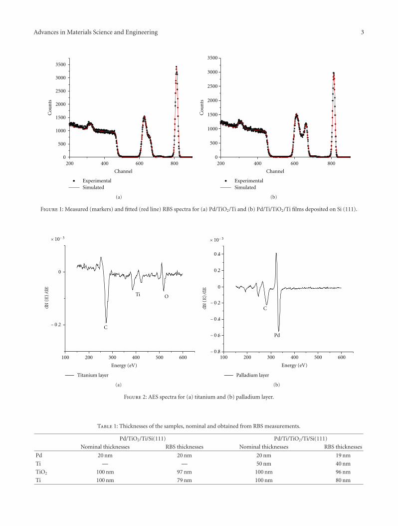
Advances in Materials Science and Engineering 3
3500
3000
2500
2000
1500
1000
500
0
Cou
nts
ExperimentalSimulated
200 400 600 800
Channel
(a)
3500
3000
2500
2000
1500
1000
500
0
Cou
nts
ExperimentalSimulated
200 400 600 800
Channel
(b)
Figure 1: Measured (markers) and fitted (red line) RBS spectra for (a) Pd/TiO2/Ti and (b) Pd/Ti/TiO2/Ti films deposited on Si (111).
0
Ti O
C
Titanium layer
− 0.2
× 10− 3
Energy (eV)
100 200 300 400 500 600
dN
(E)/dE
(a)
C
0
− 0.2
− 0.4
0.2
0.4
− 0.6
− 0.8
× 10− 3
Pd
Palladium layer
Energy (eV)
100 200 300 400 500 600
dN
(E)/dE
(b)
Figure 2: AES spectra for (a) titanium and (b) palladium layer.
Table 1: Thicknesses of the samples, nominal and obtained from RBS measurements.
Pd/TiO2/Ti/Si(111) Pd/Ti/TiO2/Ti/Si(111)
Nominal thicknesses RBS thicknesses Nominal thicknesses RBS thicknesses
Pd 20 nm 20 nm 20 nm 19 nm
Ti — — 50 nm 40 nm
TiO2 100 nm 97 nm 100 nm 96 nm
Ti 100 nm 79 nm 100 nm 80 nm
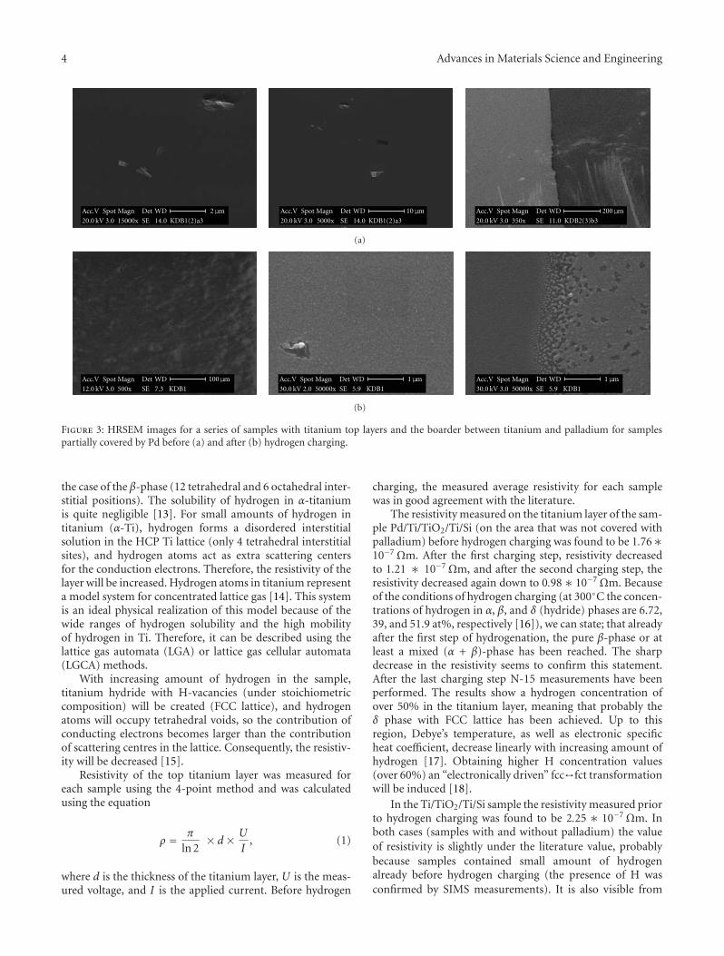
4 Advances in Materials Science and Engineering
Acc.V Spot Magn Det WD
20.0 kV 3.0 SE
Acc.V Spot Magn Det WD 2μm
20.0 kV 3.0 15000x SE 14.0 KDB1(2)a3
200μm
350x
Acc.V Spot Magn Det WD
20.0 kV 3.0 5000x SE 14.0 KDB1(2)a3
10μm
11.0 KDB2(3)b3
(a)
Acc.V Spot Magn Det WD
SE KDB1
Acc.V Spot Magn Det WD
SE KDB1
100μm 1μm
500x 50000x7.3 5.912.0 kV 3.0
Acc.V Spot Magn Det WD
SE KDB1
1μm
50000x 5.930.0 kV 3.030.0 kV 2.0
(b)
Figure 3: HRSEM images for a series of samples with titanium top layers and the boarder between titanium and palladium for samplespartially covered by Pd before (a) and after (b) hydrogen charging.
the case of the β-phase (12 tetrahedral and 6 octahedral inter-stitial positions). The solubility of hydrogen in α-titaniumis quite negligible [13]. For small amounts of hydrogen intitanium (α-Ti), hydrogen forms a disordered interstitialsolution in the HCP Ti lattice (only 4 tetrahedral interstitialsites), and hydrogen atoms act as extra scattering centersfor the conduction electrons. Therefore, the resistivity of thelayer will be increased. Hydrogen atoms in titanium representa model system for concentrated lattice gas [14]. This systemis an ideal physical realization of this model because of thewide ranges of hydrogen solubility and the high mobilityof hydrogen in Ti. Therefore, it can be described using thelattice gas automata (LGA) or lattice gas cellular automata(LGCA) methods.
With increasing amount of hydrogen in the sample,titanium hydride with H-vacancies (under stoichiometriccomposition) will be created (FCC lattice), and hydrogenatoms will occupy tetrahedral voids, so the contribution ofconducting electrons becomes larger than the contributionof scattering centres in the lattice. Consequently, the resistiv-ity will be decreased [15].
Resistivity of the top titanium layer was measured foreach sample using the 4-point method and was calculatedusing the equation
ρ = π
ln 2× d × U
I, (1)
where d is the thickness of the titanium layer, U is the meas-ured voltage, and I is the applied current. Before hydrogen
charging, the measured average resistivity for each samplewas in good agreement with the literature.
The resistivity measured on the titanium layer of the sam-ple Pd/Ti/TiO2/Ti/Si (on the area that was not covered withpalladium) before hydrogen charging was found to be 1.76∗10−7 Ωm. After the first charging step, resistivity decreasedto 1.21 ∗ 10−7 Ωm, and after the second charging step, theresistivity decreased again down to 0.98∗ 10−7 Ωm. Becauseof the conditions of hydrogen charging (at 300◦C the concen-trations of hydrogen in α, β, and δ (hydride) phases are 6.72,39, and 51.9 at%, respectively [16]), we can state; that alreadyafter the first step of hydrogenation, the pure β-phase or atleast a mixed (α + β)-phase has been reached. The sharpdecrease in the resistivity seems to confirm this statement.After the last charging step N-15 measurements have beenperformed. The results show a hydrogen concentration ofover 50% in the titanium layer, meaning that probably theδ phase with FCC lattice has been achieved. Up to thisregion, Debye’s temperature, as well as electronic specificheat coefficient, decrease linearly with increasing amount ofhydrogen [17]. Obtaining higher H concentration values(over 60%) an “electronically driven” fcc↔fct transformationwill be induced [18].
In the Ti/TiO2/Ti/Si sample the resistivity measured priorto hydrogen charging was found to be 2.25 ∗ 10−7 Ωm. Inboth cases (samples with and without palladium) the valueof resistivity is slightly under the literature value, probablybecause samples contained small amount of hydrogenalready before hydrogen charging (the presence of H wasconfirmed by SIMS measurements). It is also visible from

Advances in Materials Science and Engineering 5
Figure 4 that the resistivity is lower for samples covered bypalladium (because of the supporting role of Pd for hydrogendissociation and diffusion into the metal). However, laterboth curves are decreasing almost parallel. After the firstcharging step, it decreased to 2.17 ∗ 10−7 Ωm, after thesecond charging step it decreased to 1.88 ∗ 10−7 Ωm, andafter the last charging it decreased to 1.63 ∗ 10−7 Ωm. thischange in the resistivity suggests that after the first process ofcharging the (α + β)- or β-phase was achieved and after thesecond process the pure β-phase was obtained. Further N-15measurements showed about 40% of hydrogen in the sample,meaning that in this case the δ phase has not been reached.
Because their resistance can be switched reversibly byan applied electric field, metal-insulator-metal (MIM) stru-ctures such as Ti/TiO2/Ti have been proposed for resistiverandom-access memories (ReRAM) [19]. However, methodsfor improving the uniformity of resistive switching parame-ters will be yet studied. Yingtao Li et al. [20] reported nitro-gen annealing as a method improving the broad variationsof the resistive switching parameters in the as-depositedTiOx films. Changing the resistivity of titanium by hydrogencharging could also be a way to modify properties of suchsystems.
3.4. Hydrogen Profiling. To obtain the hydrogen profiles insamples Pd/Ti/TiO2/Ti/Si(111) and Ti/TiO2/Ti/Si (111) withthe same titanium layer thicknesses and the same hydrogencharging times and temperature, SIMS and N-15 measure-ments have been performed.
For those samples, partially covered by palladium, it isclearly visible that hydrogen charging enhanced the hydrogenconcentration (storage) in both (top and bottom) titaniumlayers, but no changes were observed in the oxide layer.
Titanium is a metal that was widely investigated as apotential material for hydrogen storage, because of its highhydrogen storage capacity (67%) and its very low outgassingproperty [21]. In the titanium-hydrogen system, the heatof solution and the formation energy of the hydride, TiH2,are both negative [22]. At elevated temperatures, hydrogenatoms in the titanium formed hydrides immediately. Thehydride formation is therefore controlled by the diffusionprocess of the hydrogen atoms, and numerical calculationsconcerning this topic have also been performed, and sometheoretical models have been developed [23, 24]. One ofthese models is based on the idea that complex defectswill contribute to the surface diffusion flux at temperaturesapproaching the melting point and allows determining dif-fusion coefficient even in the case of very complex and defect-ed systems.
Results presented here show that after charging the con-centration of hydrogen was increased in titanium layers;however, in the titanium dioxide layer its concentration re-mains the same as before (Figures 5 and 6(a)). Results ofN-15 measurements show an accumulation of hydrogen inboth titanium layers (up to 50%) but only a small amount(less than 5%) in the oxide layer. These results are in goodagreement with results of SIMS measurements (Figure 6). Itseems to be clear that hydrogen diffuses through the oxide
2.4
2.2
2
1.8
1.6
1.4
1.2
1
0.8
× 10− 7
Time (hours)
0 2 4 6 8 10 12 14 16 18 20 22
Res
isti
vity
(Ωm
)
Figure 4: Charging time dependence of resistivity in titanium layer.
layer without any accumulation there. This fact can be ex-plained by the mechanism, proposed by Bates et al. [25], whodescribed the diffusion of hydrogen and its isotopes througha TiO2 sample in direction parallel and perpendicular to thec axis. They showed that because of its large open channelsparallel to the c axis, diffusion of hydrogen is very rapid inthis direction and proceeds by a proton jump from one O2−
ion to another along this channel (so diffusion parallel to thec axis is much faster than in the perpendicular direction).
For a sample without palladium layer, the situation isquite similar and differs only in the contents of hydrogen.Prior to charging some amount of hydrogen was observed bySIMS measurements because of the H absorption of the sur-face. Charging with hydrogen increased this amount in thetop titanium layer significantly, but in the second titaniumlayer the concentration of hydrogen remains lower than inthe case of the sample with palladium top layer (Figure 7).This result indicates that palladium acts as a catalyst for ga-thering hydrogen in Ti and its diffusion through the TiO2
layer.Results of N-15 measurements show a high accumulation
of hydrogen in the first titanium layer (∼40%) and a smalleramount in the second titanium layer (∼15%). Only a verysmall amount of hydrogen was observed in the oxide layer.This indicates that the lack of palladium on the top hindershydrogen to penetrate into titanium, as well as into the sec-ond Ti layer through the titanium dioxide layer [3]. Pd sup-ports the dissociation of H2 molecules on the surface. Hav-ing Pd metal atoms on the surface, they can promote thedissociation of hydrogen molecules, and so the H atomscan be easily absorbed by the bulk of the metal and diffusethrough other layers. These results are in good agreementwith concentration depth profiles from SIMS measurements.
4. Summary
In this study, the main characteristics of hydrogen absorptionby titanium and titanium dioxide thin films were investigated

6 Advances in Materials Science and Engineering
Cou
nts
Depth (nm)
1000
100
10
1
0.1
0.01
× 103
0 50 100 150 200 250
(a)
HO
Pd
SiTi
Cou
nts
100
10
1
0.1
0.01
× 103
0 50 100 150 200 250
Depth (nm)
(b)
Figure 5: SIMS profiles for the sample Pd/Ti/TiO2/Ti/Si before (a) and after (b) hydrogen charging.
1000
100
Cou
nts
Depth (nm)
0 50 100 150 200 250
H afterH before
(a)
H concentration
60
50
40
30
20
10
00 100 200 300
Depth (nm)
Hco
nce
ntr
atio
n(%
)
(b)
Figure 6: Comparison of H profiles for the sample Pd/Ti/TiO2/Ti/Si measured by SIMS (a) and N-15 (b).
with specific emphasis on the hydrogen diffusion and its stor-age in each layer. It is clearly visible from the results that pal-ladium acts as a catalyst for hydrogen diffusion through TiO2
layer and increases the maximum H concentration up toa value of over 50% (under the palladium-covered part)instead of about 20% in titanium if it is not covered by pal-ladium. Hydrogen profiles obtained both by SIMS and N-15measurements proved this higher hydrogen concentrationsin good agreement in samples with partially covered toplayers. Concerning the surface, hydrogen charging caused agranulation of titanium layer. Also the palladium layer waschanged (cracks on the surface) because of the elevated
temperatures during the hydrogen charging process. The re-sistivity of the samples has decreased with increasing hydro-gen charging according to the predictions as it was pointedout in the discussion.
Acknowledgments
This work was supported by MPD Programme “Krakow In-terdisciplinary PhD-Project in Nanoscience and AdvancedNanostructures” operated within the Foundation for PolishScience and cofinanced by the EU European Regional Devel-opment Fund. Authors thank J. Gassmann (Institute of

Advances in Materials Science and Engineering 7
Cou
nts
Depth (nm)
1000
100
10
1
0.1
0.01
× 103
0 50 100 150 200 2500.001
(a)
Cou
nts
Depth (nm)
1000
100
10
1
0.1
0.01
× 103
0 50 100 150 200 2500.001
HO
SiTi
(b)
Figure 7: SIMS profiles for the sample Ti/TiO2/Ti/Si before (a) and after (b) hydrogen charging.
1000
100Cou
nts
Depth (nm)
0 50 100 150 200 250
H afterH before
10
(a)
H concentration
50
40
30
20
10
00 100 200 300
Depth (nm)
50 150 250
Hco
nce
ntr
atio
n(%
)
(b)
Figure 8: Hydrogen profiles for the sample Ti/TiO2/Ti/Si measured by SIMS (a) and by N-15 (b).
Materials Science, Technische Universitat Darmstadt) for hisassistance at resistivity measurements and M. Perzanowski(Institute for Nuclear Physics, Polish Academy of Sciences)for preparing the palladium cover layers.
References
[1] M. Maaza, Z. Jiang, F. Samuel, B. Farnoux, and B. Vidal, “Im-provement of neutron reflectivity of an Ni-Ti multilayer byhydrogenation of titanium layers,” Journal of Applied Crysta-llography, vol. 25, no. 6, pp. 789–796, 1992.
[2] Z. Qin and D. W. Shoesmith, “Failure model and Monte Carlosimulations for titanium (grade-7) drip shields under Yucca
Mountain repository conditions,” Journal of Nuclear Materials,vol. 379, no. 1–3, pp. 169–173, 2008.
[3] Z. Qin, Y. Zeng, P. R. Norton, and D. W. Shoesmith, “Modelinghydrogen permeation through a thin TiO2 film deposited onPd using COMSOL multiphysics,” in Proceedings of the 5thCOMSOL Conference, Boston, Mass, USA, 2009.
[4] B. G. Pound, “Hydrogen ingress in titanium,” Corrosion, vol.47, no. 2, pp. 99–104, 1991.
[5] S. I. Pyun, J. W. Park, and Y. G. Yoon, “Hydrogen permeationthrough PECVD (plasma-enhanced chemical vapor deposi-tion) TiO2 film on Pd by the time lag method,” Journal of Alloysand Compounds, vol. 231, no. 1-2, pp. 315–320, 1995.
[6] H. Numakura, Nippon Kinzoku Gakkai Kaihou, vol. 31, p. 525,1992.

8 Advances in Materials Science and Engineering
[7] A. Brudnik, H. Czternastek, K. Zakrzewska, and M. Jachi-mowski, “Plasma-emission-controlled d.c. magnetron sput-tering of TiO2-x thin films,” Thin Solid Films, vol. 199, no. 1,pp. 45–58, 1991.
[8] A. Trenczek-Zajac, M. Radecka, K. Zakrzewska et al., “Struc-tural and electrical properties of magnetron sputtered Ti(ON)thin films: the case of TiN doped in situ with oxygen,” Journalof Power Sources, vol. 194, no. 1, pp. 93–103, 2009.
[9] N. T. H. Kim-Ngan, A. G. Balogh, J. D. Meyer et al., “Thermaland irradiation induced interdiffusion in magnetite thin filmsgrown on magnesium oxide (0 0 1) substrates,” Surface Science,vol. 603, no. 9, pp. 1175–1181, 2009.
[10] M. Mayer, AIP Conference Proceedings, vol. 475, pp. 541–544, 1999, SIMNRA (Simulation Program for the Analysis ofNRA, RBS and ERDA) developed by M. Mayer http://www.rzg.mpg.de/∼mam/.
[11] N. P. Barradas, “Double scattering in grazing angle Rutherfordbackscattering spectra,” Nuclear Instruments and Methods inPhysics Research B, vol. 225, no. 3, pp. 318–330, 2004.
[12] S. Nakao, K. Saitoh, T. Hirahara et al., “Preparation andoptical transmittance of titanium hydride (deuteride) films byrf reactive sputtering,” Thin Solid Films, vol. 343-344, no. 1-2,pp. 195–198, 1999.
[13] N. E. Paton and J. C. Williams, in Effectof Hydrogen on Behaviorof Materials, A. W. Thompson and I. M. Bernstein, Eds., p. 409,AIME, New York, NY, USA, 1976.
[14] H. Wipf, B. Kappesser, and R. Werner, “Hydrogen diffusion intitanium and zirconium hydrides,” Journal of Alloys and Com-pounds, vol. 310, no. 1-2, pp. 190–195, 2000.
[15] K. Kandasamy and N. A. Surplice, “The effects of hydrogensorption on the resistance and work-function of titaniumfilms at 290K,” Journal of Physics D, vol. 17, no. 2, pp. 387–398,1984.
[16] E. Tal-Gutelmacher, R. Gemma, A. Pundt, and R. Kirchheim,“Hydrogen absorption in ion beam sputtered titanium thinfilms,” Defect and Diffusion Forum, vol. 283–286, pp. 662–668,2009.
[17] K. Bohmhammel, G. Wolf, G. Gross, and H. Madge, “Investi-gations of the molar heat capacity at low temperatures in theTiHx system,” Journal of Low Temperature Physics, vol. 43, no.5-6, pp. 521–532, 1981.
[18] A. C. Switendick, “Influence of the electronic structure on thetitanium-vanadium-hydrogen phase diagram,” Journal of TheLess-Common Metals, vol. 49, pp. 283–290, 1976.
[19] B. J. Choi, D. S. Jeong, S. K. Kim et al., “Resistive switchingmechanism of TiO2 thin films grown by atomic-layer depo-sition,” Journal of Applied Physics, vol. 98, no. 3, Article ID033715, pp. 1–10, 2005.
[20] Y. Li, Y. Wang, S. Liu et al., “Improvement of resistive switch-ing uniformity in TiOx films by nitrogen annealing,” Journal ofthe Korean Physical Society, vol. 58, no. 3, pp. 407–410, 2011.
[21] M. Takeda, H. Kurisu, S. Yamamoto, and H. Nakagawa, “Hyd-rogen distribution in titanium materials with low outgassingproperty,” Vacuum, vol. 84, no. 2, pp. 352–356, 2009.
[22] Y. Fukai, The Metal–Hydrogen System, Springer, New York, NY,USA, 1993.
[23] K. Mizuno, Y. Furuya, K. Hirano, and H. Okamoto, “Hydrogendiffusion in titanium-hydride observed by the diffraction-enhanced X-ray imaging method,” Physica Status Solidi (A),vol. 204, no. 8, pp. 2734–2739, 2007.
[24] P. G. Shewmon, Diffusion in Solid, MacGraw-Hill, New York,NY, USA, 1963.
[25] J. B. Bates, J. C. Wang, and R. A. Perkins, “Mechanisms forhydrogen diffusion in TiO2,” Physical Review B, vol. 19, no. 8,pp. 4130–4139, 1979.
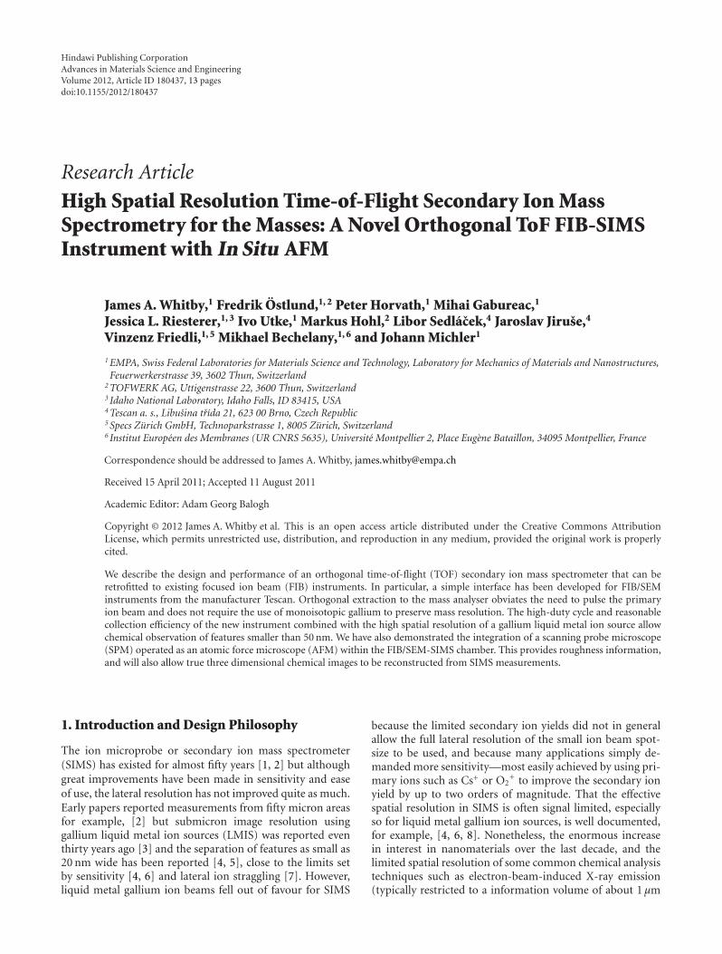
Hindawi Publishing CorporationAdvances in Materials Science and EngineeringVolume 2012, Article ID 180437, 13 pagesdoi:10.1155/2012/180437
Research Article
High Spatial Resolution Time-of-Flight Secondary Ion MassSpectrometry for the Masses: A Novel Orthogonal ToF FIB-SIMSInstrument with In Situ AFM
James A. Whitby,1 Fredrik Ostlund,1, 2 Peter Horvath,1 Mihai Gabureac,1
Jessica L. Riesterer,1, 3 Ivo Utke,1 Markus Hohl,2 Libor Sedlacek,4 Jaroslav Jiruse,4
Vinzenz Friedli,1, 5 Mikhael Bechelany,1, 6 and Johann Michler1
1 EMPA, Swiss Federal Laboratories for Materials Science and Technology, Laboratory for Mechanics of Materials and Nanostructures,Feuerwerkerstrasse 39, 3602 Thun, Switzerland
2 TOFWERK AG, Uttigenstrasse 22, 3600 Thun, Switzerland3 Idaho National Laboratory, Idaho Falls, ID 83415, USA4 Tescan a. s., Libusina trıda 21, 623 00 Brno, Czech Republic5 Specs Zurich GmbH, Technoparkstrasse 1, 8005 Zurich, Switzerland6 Institut Europeen des Membranes (UR CNRS 5635), Universite Montpellier 2, Place Eugene Bataillon, 34095 Montpellier, France
Correspondence should be addressed to James A. Whitby, [email protected]
Received 15 April 2011; Accepted 11 August 2011
Academic Editor: Adam Georg Balogh
Copyright © 2012 James A. Whitby et al. This is an open access article distributed under the Creative Commons AttributionLicense, which permits unrestricted use, distribution, and reproduction in any medium, provided the original work is properlycited.
We describe the design and performance of an orthogonal time-of-flight (TOF) secondary ion mass spectrometer that can beretrofitted to existing focused ion beam (FIB) instruments. In particular, a simple interface has been developed for FIB/SEMinstruments from the manufacturer Tescan. Orthogonal extraction to the mass analyser obviates the need to pulse the primaryion beam and does not require the use of monoisotopic gallium to preserve mass resolution. The high-duty cycle and reasonablecollection efficiency of the new instrument combined with the high spatial resolution of a gallium liquid metal ion source allowchemical observation of features smaller than 50 nm. We have also demonstrated the integration of a scanning probe microscope(SPM) operated as an atomic force microscope (AFM) within the FIB/SEM-SIMS chamber. This provides roughness information,and will also allow true three dimensional chemical images to be reconstructed from SIMS measurements.
1. Introduction and Design Philosophy
The ion microprobe or secondary ion mass spectrometer(SIMS) has existed for almost fifty years [1, 2] but althoughgreat improvements have been made in sensitivity and easeof use, the lateral resolution has not improved quite as much.Early papers reported measurements from fifty micron areasfor example, [2] but submicron image resolution usinggallium liquid metal ion sources (LMIS) was reported eventhirty years ago [3] and the separation of features as small as20 nm wide has been reported [4, 5], close to the limits setby sensitivity [4, 6] and lateral ion straggling [7]. However,liquid metal gallium ion beams fell out of favour for SIMS
because the limited secondary ion yields did not in generalallow the full lateral resolution of the small ion beam spot-size to be used, and because many applications simply de-manded more sensitivity—most easily achieved by using pri-mary ions such as Cs+ or O2
+ to improve the secondary ionyield by up to two orders of magnitude. That the effectivespatial resolution in SIMS is often signal limited, especiallyso for liquid metal gallium ion sources, is well documented,for example, [4, 6, 8]. Nonetheless, the enormous increasein interest in nanomaterials over the last decade, and thelimited spatial resolution of some common chemical analysistechniques such as electron-beam-induced X-ray emission(typically restricted to a information volume of about 1 μm

2 Advances in Materials Science and Engineering
diameter by electron scattering) have prompted a new lookat high spatial resolution SIMS [9, 10]. A further motivationto re-examine the use of a gallium LMIS for SIMS is theincreasingly widespread adoption of Focused Ion Beam (FIB)instruments for sample preparation (both milling and depo-sition). These almost universally use gallium LMIS beamsto achieve excellent spatial resolutions with a high beambrightness (corresponding to acceptable milling speeds). Thecoupling of a secondary ion mass spectrometer to a dedicatedFIB instrument has been previously described by others forexample, [5, 11, 12].
Advantages of the combination of a FIB/SEM with aSIMS include excellent sample imaging (secondary electronsfrom either electron or ion beams, the latter giving betterchannelling contrast) and positioning, and the use of theFIB to precisely expose buried regions of interest for furtheranalysis by SIMS (and other techniques). It is far morecommon for FIB/SEM instruments to be designed from thestart to accommodate extra analytical techniques such asEDX, EBSD, and cathodoluminescence. and these additionaltechniques which are complementary to SIMS can be decisivein answering analytical questions posed by complex samples.Having several types of analytical measurement possible witha single vacuum chamber is not only a great time and mon-ey saver, but also avoids uncertainty due to atmosphericcontamination. The advantages of SIMS measurements overthe EDX measurements more commonly found on FIB/SEMinstruments are (i) better limits of detection (including fewerinterferences for light elements), (ii) better spatial resolution,(iii) ability to make isotopic and molecular measurements.It is, however, more difficult in general to quantify SIMSmeasurements than is the case for EDX measurements onsufficiently large and thick materials.
In this paper, we describe an implementation of an FIB-SIMS instrument and show examples of measurements madewith the prototype. Our focus has not been upon the bestpossible SIMS performance, but rather upon a pragmatic,cost-effective approach to sub-μm resolution chemical imag-ing that take as its starting points a standard commercialFIB instrument and a tried and tested mass analyser design.The FIB-SIMS functionality was developed as part of theEuropean Union funded FIBLYS (see http://www.fiblys.eu/)project which aims to create a modular suite of analyticalinstruments which can be fitted to an optimised FIB/SEMchamber. A consequence of the decision to use a commercialFIB/SEM instrument is that the vacuum chamber is onlydesigned to work at high vacuum (above 10−6 mbar) ratherthan the ultrahigh vacuum usual for secondary ion massspectrometers. The implications of this are discussed belowin the performance section.
2. The Instrument
The FIB/SEM chamber, columns, and FIB/SEM software arecommercially available parts from Tescan a.s. (a Vela SEMfitted with a FIB column using a liquid metal gallium ionsource). The mass spectrometer is a commercial orthogo-nal extraction time-of-flight instrument from Tofwerk AG(model C-TOF) with a 0.5 m nominal drift length, including
ToF mass analyser
Turbo pumpfor ToF
Pulser
Pre-amp
Primary ion (FIB) column
Figure 1: A closer look at the mass analyser in position on the backof the chamber; there is very little space available. The turbo pumpon the mass analyser (to protect the detector) will be replaced byan ion pump. The pulser electronics for the orthogonal extractionare placed close to the mass analyser in order to preserve the pulseshape.
the reflectron. This mass spectrometer was chosen becauseof its compact dimensions (see Figures 1 and 2) and becauseof the performance advantages and price/performance ratioof time-of-flight mass analysis compared to quadrupolemass analysis (as the samples expected to be studied byFIB-SIMS instruments are often very small and unique,the simultaneous detection of all masses in a time-of-flightinstrument offers efficiency gains compared to scanninga quadrupole filter). Because of the small size of theinstrument, the mass resolving power M/ΔM (FWHM) isno more than 800 at 69 Th, just sufficient to distinguishmany molecular interferences from isobaric monatomicions (Th denotes the unit Thomson for charge to massratio [13]). Orthogonal extraction [14], typically using a2 μs pulse, provides a high effective duty cycle and moreimportantly avoids the need to pulse the primary beam (forTOF operation) or to use monoisotopic gallium (necessaryto preserve mass resolution when pulsing the primary beamto define the TOF start signal), thus no changes to theFIB hardware are necessary. Secondary ions are detected inthe mass spectrometer using a pair of chevron mountedmicrochannel plates (Photonis) and the resulting analoguesignal passed through a preamplifier, an amplifier/constantfraction discriminator (RoentDek ATR19-2) and time-to-digital converter (Cronologic GmbH HPTDC8-PCI) beforebeing passed to computer memory. Essentially the samemodel of mass spectrometer has been previously described inmore detail in [15] for a similar application, although in thecurrent implementation all hardware is from Tofwerk AG.Either positive or negative secondary ions can be detected,but not simultaneously. The postacceleration voltage towards

Advances in Materials Science and Engineering 3
SEM column
Sample stage
FIB columnSecondary electrondetector
Collection lensfor TOFMS
Extraction to TOFMS
Figure 2: Interior of FIB/SEM-SIMS prototype. The sample stagehas been lowered to make the arrangement of the collection lensand charged particle columns clearer. For SIMS work, the sampleis usually positioned at a working distance of 9 mm below theSEM column, and tilted to 55◦ to present the sample surfacenormal to the incident gallium ions. Additional instrumentationsuch as nanomanipulators, gas injection systems, and EDX or BSEdetectors can be added as required. For SPM measurements, theSPM assembly was mounted on the sample stage.
the microchannel plate detector is typically 5 kV, highenough to still give detection efficiencies of about 20% forions with masses up to 2000 Da [16].
In order to make secondary ion measurements possible,collection and transfer ion topics were designed and built totake ions from the sample to the mass analyser (mountedon a flange of the FIB/SEM chamber). A set of Einzel lensesacting as relay lenses is used to transmit ions from thecollection optics to the mass analyzer; all potentials are below200 V. A grounded shroud around the collection lens is usedto improve collection efficiency and to minimize electrostaticdisturbance to other instruments in the chamber. WhenSIMS measurements are not required, the front part of theextraction ion optics nearest the sample and pole piecessimply clips off (labelled “collection lens” in Figure 2), thusallowing the full range of sample sizes to be used by the FIB.For SIMS operation, it is advantageous to extend the ionoptics so that the entrance aperture is nearer to the sampleand ion beam: in the current design, the collection opticsextend to within 8 mm of the sample/primary ion beamintersection. This leaves enough space for simultaneousoperation of the SIMS functionality with a scanning probemicroscope or gas injection system (e.g., for focused ionbeam induced processing).
To collect mass spectra, software was written to (i) con-trol the functions of the mass spectrometer, (ii) to initiate
an appropriate scan series by the FIB, and (iii) to collectsecondary electron images in parallel with the secondaryion mass spectra. The same software is used to view andanalyse the mass spectra and to export the results in otherformats (as ion images, mass spectra from selected regions,or raw data). All data are stored using the publicly availableHDF5 file standard [17] which is supported by many dataanalysis packages such as Matlab, IDL, and Igor Pro. TheTOF-SIMS software is, for performance reasons, hosted ona separate computer to that which controls the FIB/SEM.The two computers communicate via Tescan proprietaryprotocols using an Ethernet connection. Custom electronicsand a timer card from National Instruments (model NI6602)are used to adapt hardware signals from the FIB/SEM (e.g.,level shifting, logic operations, resynchronisation of clockcycles) in order to control the time-to-digital converter cardand mass spectrometer extraction pulser.
During operation, the user uses the FIB/SEM to locatethe point of interest and to adjust focus and magnification.Then, the desired image resolution, dwell time (mass tocharge range) and number of frames are selected on thecomputer hosting the mass spectrometer software and themeasurement is started from the latter. All triggers from thesubsequent acquisition series are generated by the FIB/SEMinstrument until the predetermined number of frames hasbeen reached or the measurement is stopped manually. TheFIB beam remains at each point in a frame for the defineddwell time before rapidly moving to the next point. Thebeam is not blanked during the move between neighbouringpoints, but between lines and frames it is. Although the SIMScapability has only been tested with FIB/SEM instrumentsfrom Tescan, it should be possible to fit the mass analysishardware into instruments from other manufacturers, butthe software and signalling interfaces might have to be modi-fied. Example results and different ways of displaying the dataare shown in Figures 4, 5, and 6 for a nickel finder grid.
A note on nomenclature: we refer to one complete x-yraster of the primary beam when collecting SIMS data asa “frame”. Each frame is composed of data from an evenlyspaced Cartesian grid of points projected onto the samplesurface. From each of these points, one mass spectrum isobtained from one extraction cycle of the TOFMS. Becausedynamic SIMS implies sputtering, we may consider eachmeasurement point as having some depth, and thus beinga volume element or voxel. These are referred to as “rawvoxels”. In practice, because the number of ions detectedper raw voxel is rather low, these raw voxels are binnedinto “effective voxels” for visualization although the raw datais kept. It should be noted that SIMS measurements alonedo not provide depth information, thus the use of “voxel”might be argued with. The meaning of “depth profile” and“chemical image” is illustrated in Figure 3.
3. Performance
Experience with this design of mass spectrometer suggeststhat the dynamic range of the instrument is limited by in-ternal ion scattering to about eight decades (implying 10 ppbdetection limits if all secondary ions were produced with the

4 Advances in Materials Science and Engineering
Ion beam
Electronbeam
“Depth profile”
(planar structures normal to ion beam)
Electronbeam
5555 Ion beam
“Image”
(planar structures parallel to ion beam)
Figure 3: Clarification of the primary ion beam and sample orientation for the BAM L200, VCSEL, and ALD samples described in thetext, all of which have planar structures. Depth profiles are reconstructed using the middle quarter of each image slice (“frame”) in order tominimise edge effects. The resolution in the ion beam direction (depth resolution) is limited only by ion-induced mixing and rougheningand redeposition/edge effects and is in general better than the resolution in the directions normal to the ion beam (lateral resolution) whichdepends heavily on the spot size and shape.
Figure 4: Secondary ion images for sodium, nickel, and carbon from part of a nickel finder grid on an adhesive carbon patch. Field of viewis 20 × 20 microns. Oxygen flooding was used to enhance the nickel signal. Because the full dataset is three dimensional, it could be shownthat the sodium signal was only present at the surface of the sample. The colour scale intensity units are ions per raw voxel (1024 × 1024 ×178); for display purpose the data has been binned to 128 × 128 × 178).
same useful yield). In practice, for most samples integrationtimes sufficient to make 10 ppb peaks clear above the scat-tered ion background are impractical using primary ioncurrents suited to submicron resolution imaging (<200 pA).Figure 6 shows in excess of six decades of dynamic range, andFigure 7 shows a calibration curve for boron in silicon fromwhich a limit of detection of 5.5 ppm is inferred. The limit ofdetection is a strong function of the secondary ion yield, so itwill vary for different secondary ions and matrices.
The useful ion yield was calculated for aluminium sec-ondary ions from a distributed Bragg reflector (DBR) struc-ture consisting of alternating AlGaAs and GaAs layers ofknown thickness (see Figure 12), and a figure of 4 ×10⁻⁶ detected ions per sputtered atom was obtained usinga primary ion energy of 20 keV. We are not aware ofa comparable useful yield measurement in the literaturefor the same material and primary ion beam. It is wellknown that secondary ion yields vary enormously with theion and matrix (as well as primary ion element, energy,and incident angle) and surface quality. Useful ion yieldsare further dependent upon the tuning of the mass analyserand extraction optics (it is for example common practice touse an energy filter to suppress polyatomic ions despite the
resulting reduction in useful ion yield for the analyte ions); acomparison to the (sparse) literature is, therefore, somewhatdifficult. Reported values for useful ion yields for galliumion SIMS include 1.4 × 10⁻² for Si+ from silicon oxide, 6 ×10⁻⁵ for Si+ from silicon, 1.93 × 10⁻³ for In+ from indiumphosphide and 7.8 × 10⁻⁶ for P+ from indium phosphide[18, 19]. Bearing in mind that aluminium ions seem to bedetected more sensitively than most on our instrument andthat the chamber pressure is always above 4 × 10⁻⁶ mbar(and so some signal enhancement due to oxygen possible)and there is a suggestion that the observed useful ionyield could be improved. We did not use silicon or silicondioxide to calculate a useful ion yield, because it was notpossible to obtain a stable signal under normal conditionsat the pressure used in the instrument described here. Theimplications of high vacuum operation of a SIMS instrument(instead of ultrahigh vacuum) are discussed below.
Chemical images in which lines spaced by less than100 nm are separated have been obtained (see Figures 9 and13), and we are certain that this figure can be improved uponin future by better focussing of the FIB beam. The depthresolution can be, as expected, much better than 20 nm; seeFigure 15.
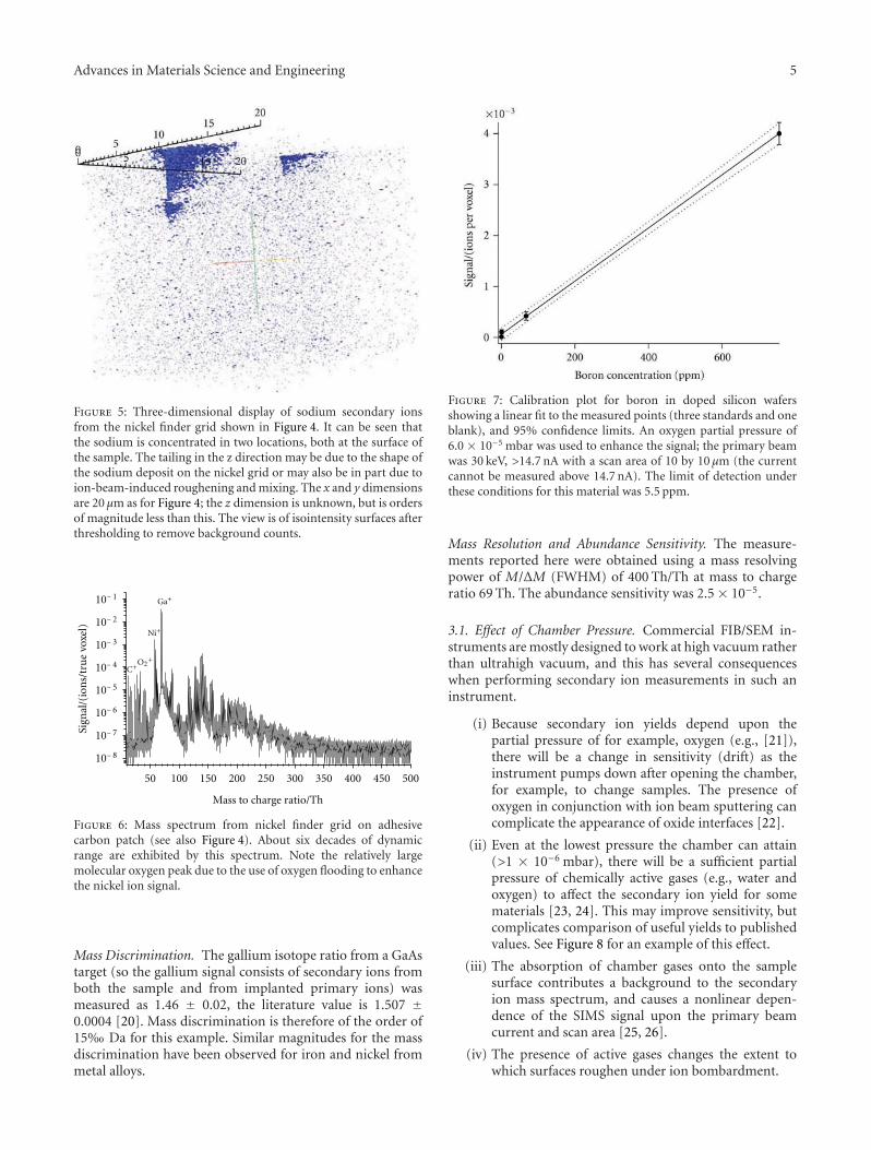
Advances in Materials Science and Engineering 5
Figure 5: Three-dimensional display of sodium secondary ionsfrom the nickel finder grid shown in Figure 4. It can be seen thatthe sodium is concentrated in two locations, both at the surface ofthe sample. The tailing in the z direction may be due to the shape ofthe sodium deposit on the nickel grid or may also be in part due toion-beam-induced roughening and mixing. The x and y dimensionsare 20 μm as for Figure 4; the z dimension is unknown, but is ordersof magnitude less than this. The view is of isointensity surfaces afterthresholding to remove background counts.
10− 8
10− 7
10− 6
10− 5
10− 4
10− 3
10− 2
10− 1
Sign
al/(
ion
s/tr
ue
voxe
l)
50045040035030025020015010050
Mass to charge ratio/Th
Ga+
Ni+
O2+
C+
Figure 6: Mass spectrum from nickel finder grid on adhesivecarbon patch (see also Figure 4). About six decades of dynamicrange are exhibited by this spectrum. Note the relatively largemolecular oxygen peak due to the use of oxygen flooding to enhancethe nickel ion signal.
Mass Discrimination. The gallium isotope ratio from a GaAstarget (so the gallium signal consists of secondary ions fromboth the sample and from implanted primary ions) wasmeasured as 1.46 ± 0.02, the literature value is 1.507 ±0.0004 [20]. Mass discrimination is therefore of the order of15‰ Da for this example. Similar magnitudes for the massdiscrimination have been observed for iron and nickel frommetal alloys.
Figure 7: Calibration plot for boron in doped silicon wafersshowing a linear fit to the measured points (three standards and oneblank), and 95% confidence limits. An oxygen partial pressure of6.0 × 10−5 mbar was used to enhance the signal; the primary beamwas 30 keV, >14.7 nA with a scan area of 10 by 10 μm (the currentcannot be measured above 14.7 nA). The limit of detection underthese conditions for this material was 5.5 ppm.
Mass Resolution and Abundance Sensitivity. The measure-ments reported here were obtained using a mass resolvingpower of M/ΔM (FWHM) of 400 Th/Th at mass to chargeratio 69 Th. The abundance sensitivity was 2.5 × 10⁻⁵.
3.1. Effect of Chamber Pressure. Commercial FIB/SEM in-struments are mostly designed to work at high vacuum ratherthan ultrahigh vacuum, and this has several consequenceswhen performing secondary ion measurements in such aninstrument.
(i) Because secondary ion yields depend upon thepartial pressure of for example, oxygen (e.g., [21]),there will be a change in sensitivity (drift) as theinstrument pumps down after opening the chamber,for example, to change samples. The presence ofoxygen in conjunction with ion beam sputtering cancomplicate the appearance of oxide interfaces [22].
(ii) Even at the lowest pressure the chamber can attain(>1 × 10⁻⁶ mbar), there will be a sufficient partialpressure of chemically active gases (e.g., water andoxygen) to affect the secondary ion yield for somematerials [23, 24]. This may improve sensitivity, butcomplicates comparison of useful yields to publishedvalues. See Figure 8 for an example of this effect.
(iii) The absorption of chamber gases onto the samplesurface contributes a background to the secondaryion mass spectrum, and causes a nonlinear depen-dence of the SIMS signal upon the primary beamcurrent and scan area [25, 26].
(iv) The presence of active gases changes the extent towhich surfaces roughen under ion bombardment.

6 Advances in Materials Science and Engineering
4
3
2
1
0
En
han
cem
ent
fact
orw
ith
oxyg
en
22
× 10− 6
2018161412108
Pressure (mbar)
Figure 8: Effect of oxygen flow rate on SIMS signal for a cobaltalloy; the graph shows the Co+ secondary ion signal as oxygen wasbled into the chamber through a needle valve. The plot has beennormalised to the signal when the needle valve was closed (i.e., nooxygen flow, chamber pressure 6.9 × 10⁻⁶ mbar). 5 keV, 1270 pAGa+ primary beam, 10 × 10 μm scan area. It can be seen fromthe gradient that there is likely a significant oxygen enhancementeffect for cobalt secondary ions even at the lowest pressure (with nooxygen flow).
All of these effects may be minimised (but not avoidedcompletely) by venting with an inert gas or better by using aload-lock chamber. Normalisation to the gallium ion signalcan sometimes be used to correct for oxidation effects onSIMS yields [27]. In general, however, for good reproducibil-ity it is necessary to record (and to control) the pressure inthe chamber when performing SIMS measurements at highvacuum. For samples which are sensitive to the residual gasesin the chamber (e.g., silicon), we suggest deliberately addinga known partial pressure of for example, oxygen in order toimprove stability. Oxygen flooding can however have side-effects such as distortion of depth profiles [24].
4. Applications
To illustrate the performance of our first FIB-SIMS proto-type, we present here some example applications. When animage is captioned as a depth profile, it means that the datahas been integrated from a region of each x-y plane (frame)and is plotted as a function of frame number (equivalentto depth or z-direction). When an image is captioned as an“image”, it means that the x-y (frame) data is shown, and thatthe data has been integrated along the z/depth direction. Seealso Figure 3. For all of the data shown here, the primaryion beam was incident normal to the mean sample surface.Depth profiles use only the centre part of each frame in orderto minimise crater edge effects (this conservative approachthrows away 75% of the signal).
4.1. Spatial Resolution Standard BAM L200. Figure 9 showsan aluminium secondary ion image from an unmounted,
Figure 9: Aluminium secondary ion image from the BAM L200aluminium/indium/gallium arsenide standard. Field of view 2 ×2 μm, displayed pixel size 15.6 nm, 30 keV, <1 pA primary galliumion beam. Superimposed in red are the integrated profile, andlabels denoting the period of each line pair (see bam l200repe.pdffrom http://www.rm-certificates.bam.de/ for more information).The 67.5 nm period line pair (i.e., lines of width 34 nm, separatedby 34 nm) is barely split, but the 97 nm period pair (49 nm widelines) is well resolved.
unpolished chip of the BAM L200 resolution test referencematerial. BAM define the spatial resolution to be that ofthe smallest period grating that can be distinguished, in thiscase P7 with period 67.5 nm (the widths and separationof the aluminium rich stripes in P7 are 34 nm). The ionbeam FWHM is calculated to be about 50 nm (see below).Noteworthy is that the chemical image was achieved froma rather rough surface—the existence of surface topography(scratches from sawing the sample) did not distort the chem-ical image. It was also possible to detect (but not resolve) thesingle aluminium rich stripes W8 (38 nm), W5 (19. nm) W10(14.2 nm) and W9 (3.6 nm). In a round-robin study of SIMSresolution [10] only ten out of sixteen laboratories coulddetect a 5 nm wide aluminium rich stripe in the similar BAML002 standard, and the smallest calculated beam FWHM was69 nm.
Figure 10 shows the corresponding indium ion image.The signal here is nosier both because indium is lesssensitively detected than aluminium from this material andbecause the indium-rich stripes are very thin (<5 nm, muchsmaller than a single pixel in this image).
The lateral resolution of an image can be defined invarious ways, as discussed by [28] and will, in general,depend also upon the signal to noise ratio of the image.The ISO definition for surface chemical analysis makes ref-erence to the distance between the 12% and 88% intensitypoints in a line scan across a well-defined step function [29].

Advances in Materials Science and Engineering 7
Figure 10: Indium positive secondary ion image from BAM L200(same data set as Figure 9). The unresolved indium features actuallyconsist of two line pairs (each with 5 nm wide indium rich lines)—the distance between the line pairs is not documented.
For a Gaussian beam, a good approximation to gallium LMISbeam spot distributions [10], this distance corresponds tothe full width at half-maximum (FWHM). Note that someFIB manufacturers prefer to use the 20% and 80% intensitypoints. Figure 11 shows the result of fitting the comple-mentary error function (the convolution of a Gaussian witha step function) to part of the aluminium profile shownin Figure 9. The aluminium rich stripe in P4 has a widthof 97 nm; just large enough compared to the spot size toregard the profile as a measured edge spread function. Areasonable fit is obtained suggesting that the beam profile iswell approximated by a Gaussian distribution. Using eitherthe ISO definition or a deconvolution of the data gives aFWHM for the primary beam of about 50 nm (the 20%–80%definition gives a spot size of about 40 nm). With experience,we expect further increases in performance, as according tothe manufacturer it should be possible to obtain this beamsize at much higher currents than we used (the specificationis for 50 pA into a 20 nm spot, or 500 pA into a 50 nm spot).
The above analysis assumes that the resolution is deter-mined by the primary beam size and not by any otherphysical processes. We can neglect lateral straggling ofprimary ions as this is of the order of a few nanometers [7],possibly up to 20 nm [9]. Although differential sputteringand the resulting increase in rugosity of the surface mightcontribute to a larger effective spot size, because secondaryion yields depend on surface roughness and the surface-primary beam angle, we do not see any change of lateralresolution with depth.
4.2. Semiconductor Laser. The performance achieved withthe BAM L200 standard is particularly relevant to applica-
Distance (nm)
440420400380360340320300280
40 nm
20%
80%
ProfileFit to profile
Figure 11: Enlargement of part of the profile from Figure 9 showinga superimposed fit of a complementary error function and the 20%and 80% points. The inferred spot size for the FIB beam (and so thespatial resolution of the SIMS signal) is between 40 and 50 nm forthis dataset.
tions involving semiconductor or photonic devices fabri-cated in gallium arsenide. Figures 12 to 14 show depth pro-files and chemical images of a Vertical Cavity Surface Emit-ting Laser constructed from an AlGaAs/GaAs DistributedBragg Reflector (DBR) fused to an AlGaInAs/InP gain wafer.The device has been previously described in more detail in[30] and was the first example of a wafer-fused semiconduc-tor disk laser operating at the 1.3 μm wavelength. The speci-men described here is denoted VECSEL 3/1. Figure 12 showsa positive secondary ion depth profile through the device.On the right hand side is part of the AlGaAs/GaAs DBRstructure (35 repeats of a 100 nm layer of GaAs and a 100 nmlayer of Al0.9Ga0.1As). On the left-hand side (left of frame 70on the x-axis) are the structures in the AlGaInAs/InP wafer.The expected structure is shown schematically in Figure 13.Although much of the compositional structure of the deviceis visible, the structure within the five quantum well regionswas not resolved. (Each of these 44 nm thick units consistsof three 10 nm thick Al0.28Ga0.26In0.46As layers separated bytwo 7 nm thick layers of Al0.14Ga0.18In0.68As; each unit isthen spaced apart by InP layers). The depth resolution inthis profile is apparently of the order of 20 nm. As reportedpreviously for a SIMS depth profile of a similar material [31]using different experimental conditions, we see a decreasein the modulation depth of the repeated layers with depth(i.e., the peak to valley difference of the aluminium signal)which was shown to be due to roughening of the surface(ripple formation [31]). The effect is less severe for theconditions reported here, consistent with the lower extent of
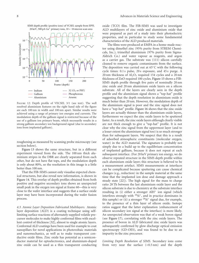
8 Advances in Materials Science and Engineering
10− 5
10− 4
10− 3
10− 2
10− 1
Inte
nsi
ty(i
ons/
pixe
l)
200150100500
Frame (depth)
IndiumGalliumAluminium
32 (O2 or PH?)PhosphorousArsenic
SIMS depth profile (positive ions) of VCSEL sample from EPFL20 keV, 500 pA Ga+ primary ions, 10 × 10 micron scan area
Figure 12: Depth profile of VECSEL 3/1 (see text). The wellresolved aluminium features on the right hand side of the figureare each 100 nm in width and 100 nm apart. Similar results wereachieved using a range of primary ion energies and currents. Themodulation depth of the gallium signal is restricted because of theuse of a gallium ion primary beam, which necessarily results in astrong gallium secondary ion background signal (due to secondaryions from implanted gallium).
roughening as measured by scanning probe microscopy (seesection below).
Figure 13 shows the same structure, but in a differentexperiment viewed from the side. The 100 nm thick alu-minium stripes in the DBR are clearly separated from eachother, but do not have flat tops, and the modulation depthis only about 80%, so the resolution in this image is a littlebetter than 100 nm.
That the FIB-SIMS cannot only visualise expected chem-ical structures, but also reveal new information, is shown inFigure 14. This overlay of depth profiles obtained from bothpositive and negative secondary ions shows an unexpectedsmall peak in the oxygen ion signal at frame 60—this is veryclose to the wafer interface and suggests that a surface oxidelayer may have been incorporated during the wafer fusionprocess.
4.3. Atomic Layer Deposition Fabricated Multilayers. Atomiclayer deposition (ALD) is a coating technique using self-limiting surface reactions of alternately supplied volatile pre-cursor molecules to make highly conformal films with excel-lent control of thickness [32], almost to single atomic layers.Conformal ALD coatings have been used for example to coatnanopillars for novel applications in photovoltaic materialsand nanomechanics, as well as to make transparent con-ductive oxide films. Zinc oxide has potential as a semicon-ductor material for optoelectronics, and aluminium-dopedzinc oxide can be used as a thin transparent conducting
oxide (TCO) film. The FIB-SIMS was used to investigateALD multilayers of zinc oxide and aluminium oxide thatwere prepared as part of a study into their photoelectricproperties, and in particular to study some fundamentalcharacteristics of the ALD produced materials.
The films were produced at EMPA in a home-made reac-tor using dimethyl zinc (95% purity from STREM Chemi-cals, Inc.), trimethyl aluminium (97% purity from Sigma-Aldrich Co.) and water vapour as reagents, and argonas a carrier gas. The substrate was (111) silicon carefullycleaned to remove organic contaminants from the surface.The deposition was carried out at 65◦C with the followingcycle times: 0.1 s pulse, 20 s exposure, and 45 s purge. A20 nm thickness of Al2O3 required 154 cycles and a 20 nmthickness of ZnO required 100 cycles. Figure 15 shows a FIB-SIMS depth profile through five pairs of nominally 20 nmzinc oxide and 20 nm aluminium oxide layers on a siliconsubstrate. All of the layers are clearly seen in the depthprofile and the aluminium signal shows a “top-hat” profilesuggesting that the depth resolution in aluminium oxide ismuch better than 20 nm. However, the modulation depth ofthe aluminium signal is poor and the zinc signal does nothave a “top-hat” profile. Figure 16 shows that the zinc oxidelayers are actually thinner than the aluminium oxide layers,furthermore we expect the zinc oxide layers to be sputteredfaster. As a result, the zinc oxide layers although clearly visibleare not thick enough to give a “top-hat” profile. It is notclear why the zinc signal from the uppermost layer (and toa lesser extent the aluminium signal too) is so much strongerthan for subsequent layers. We suspect that this is a resultof adsorbed atmospheric constituents (molecular oxygen,water) in the ALD material. The signature is probably notsimply due to a build up to the equilibrium concentrationof implanted gallium, because it does not repeat at eachsubsequent interface. (For 20 keV primary ion energy, we doobserve repeated structure in the SIMS depth profile withineach aluminium oxide layer; this structure is believed to bea measurement artefact. SIMS measurements at interfacescan be complicated because sputtering can cause chemicalchanges (e.g., reduction) in the sample material at the sametime that the implanted ion dose and damage approach asteady state [22]). The high signal for the mass to chargeratio 28 Th between the last aluminium oxide layer and thesilicon substrate is due to chemistry at the substrate interfaceresulting in (i) either a stronger AlH+ ion signal (whichinterferes strongly with 28Si+, and in practice dominates inthis sample) or (ii) a stronger 28Si+ signal due, for example,to the presence of a thin layer of silicon oxide. Isotoperatios suggest that the latter explanation (enhancement ofsilicon secondary ion signal at the interface) is more likely.An unexpected observation was that of a weak boron signal(see Figure 17), correlating with the zinc oxide layers. Thepresence of boron in ALD fabricated zinc oxide layers wassubsequently confirmed by glow discharge optical emissionspectroscopy (GD-OES), and was found to be due to animpurity in the zinc precursor.
Limiting Depth Resolution of SIMS. Secondary ions comefrom very near the surface (<0.5 nm) and the depth

Advances in Materials Science and Engineering 9
InP
(10
nm
)A
lIn
As
(80n
m)
InP
(89
nm
)
Al x
Ga 1−xIn
yA
s 1−y
(44
nm
)
Al x
Ga 1−xIn
yA
s 1−y
(44
nm
)
InP
(155
nm
)
InP
(280
nm
)
GaA
s(1
00n
m)
GaA
ssu
bstr
ate
0.001
0.01
0.1
1
10
100
0 0.5 1 1.5 2 2.5 3 3.5
AluminiumIndium-115Gallium-69
VCSEL sample observed from the edge
Aluminium
00
1
1
2
2
3
3(μm)
(μm
)
Al 0.9
Ga 0.1
As
(100
nm
)
Distance from surface (with an o set) (μm)
Figure 13: Side-on view of VECSEL 3/1 (see text). As for the depth profile, all features can be discerned, expect for the structure within eachquantum well gain region (each 44 nm thick containing three 10 nm bands richer in aluminium). The 100 nm thick aluminium rich regionsin the distributed Bragg reflector (right-hand side of figure and image) are well separated but do not have a flat-top. The lateral resolution isthus of the order of 100 nm in this example.
5
× 10− 3 × 10− 3
4
3
2
116O−
(ion
s/ra
wpi
xel)
140120100806040200Frame number
80
60
40
20
0
27A
l(i
ons/
raw
pixe
l)
Depth profile (positive and negative SIMS) for VCSEL
16O−
27Al+
+
Figure 14: Overlay of depth profiles of aluminium and oxygen forVECSEL 3/1. Note the oxygen peak at frame 60, close to the interfacebetween the two wafers. The smooth drop in the aluminium signals(not evident in Figure 12) was later discovered to be due to atemporary contamination of the ion optics.
resolution of a secondary ion depth profile, given a sufficientsignal to noise ratio, is in principle only limited by ion-induced mixing (usually of the order of a few nanometersbut can be more depending on primary ion energy and angleand sample composition) and ion-induced roughening, incommon with other techniques which use an ion beam tosputter away material in order to obtain a depth profile(e.g., XPS, Auger). Changes in the composition of the sampleusually affect secondary ion yields, and differential sputtering(in the chemical sense rather than the topographical sense)will have an effect on depth profiles at interfaces [33]. Theprocesses that limit SIMS depth resolution are discussed indetail in [34]. It is worth noting that we have no evidence forany background due to sputtered material being resputteredand ionised from the SIMS ion optics (i.e., no memoryeffect is detectable). Redeposition of material from the craterwalls onto the crater floor can affect depth profiles [34, 35],the extent to which this matters will depend upon thechemical structure of the sample, the size of the craterand the size and shape of the primary ion beam. Withappropriate mathematical models, monolayer thicknessescan be reconstructed from SIMS depth profiles [36]. Note
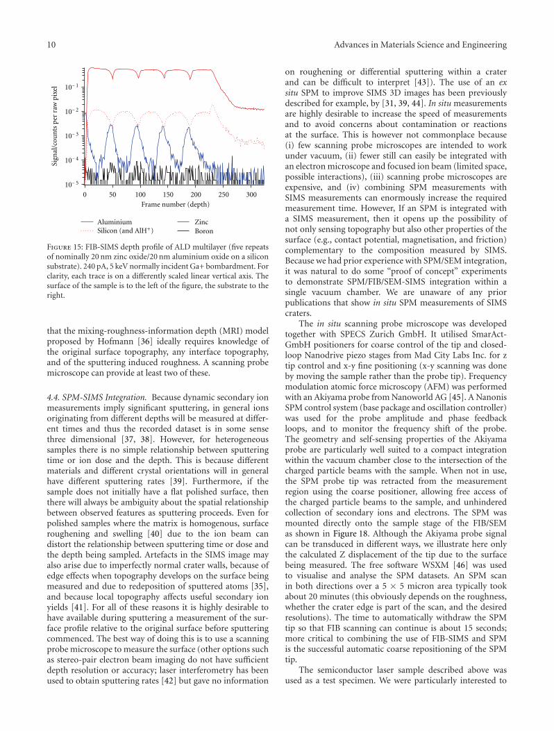
10 Advances in Materials Science and Engineering
10− 5
10− 4
10− 3
10− 2
10− 1
Sign
al/c
oun
tspe
rra
wpi
xel
300250200150100500
Frame number (depth)
AluminiumSilicon (and AlH+)
ZincBoron
Figure 15: FIB-SIMS depth profile of ALD multilayer (five repeatsof nominally 20 nm zinc oxide/20 nm aluminium oxide on a siliconsubstrate). 240 pA, 5 keV normally incident Ga+ bombardment. Forclarity, each trace is on a differently scaled linear vertical axis. Thesurface of the sample is to the left of the figure, the substrate to theright.
that the mixing-roughness-information depth (MRI) modelproposed by Hofmann [36] ideally requires knowledge ofthe original surface topography, any interface topography,and of the sputtering induced roughness. A scanning probemicroscope can provide at least two of these.
4.4. SPM-SIMS Integration. Because dynamic secondary ionmeasurements imply significant sputtering, in general ionsoriginating from different depths will be measured at differ-ent times and thus the recorded dataset is in some sensethree dimensional [37, 38]. However, for heterogeneoussamples there is no simple relationship between sputteringtime or ion dose and the depth. This is because differentmaterials and different crystal orientations will in generalhave different sputtering rates [39]. Furthermore, if thesample does not initially have a flat polished surface, thenthere will always be ambiguity about the spatial relationshipbetween observed features as sputtering proceeds. Even forpolished samples where the matrix is homogenous, surfaceroughening and swelling [40] due to the ion beam candistort the relationship between sputtering time or dose andthe depth being sampled. Artefacts in the SIMS image mayalso arise due to imperfectly normal crater walls, because ofedge effects when topography develops on the surface beingmeasured and due to redeposition of sputtered atoms [35],and because local topography affects useful secondary ionyields [41]. For all of these reasons it is highly desirable tohave available during sputtering a measurement of the sur-face profile relative to the original surface before sputteringcommenced. The best way of doing this is to use a scanningprobe microscope to measure the surface (other options suchas stereo-pair electron beam imaging do not have sufficientdepth resolution or accuracy; laser interferometry has beenused to obtain sputtering rates [42] but gave no information
on roughening or differential sputtering within a craterand can be difficult to interpret [43]). The use of an exsitu SPM to improve SIMS 3D images has been previouslydescribed for example, by [31, 39, 44]. In situ measurementsare highly desirable to increase the speed of measurementsand to avoid concerns about contamination or reactionsat the surface. This is however not commonplace because(i) few scanning probe microscopes are intended to workunder vacuum, (ii) fewer still can easily be integrated withan electron microscope and focused ion beam (limited space,possible interactions), (iii) scanning probe microscopes areexpensive, and (iv) combining SPM measurements withSIMS measurements can enormously increase the requiredmeasurement time. However, If an SPM is integrated witha SIMS measurement, then it opens up the possibility ofnot only sensing topography but also other properties of thesurface (e.g., contact potential, magnetisation, and friction)complementary to the composition measured by SIMS.Because we had prior experience with SPM/SEM integration,it was natural to do some “proof of concept” experimentsto demonstrate SPM/FIB/SEM-SIMS integration within asingle vacuum chamber. We are unaware of any priorpublications that show in situ SPM measurements of SIMScraters.
The in situ scanning probe microscope was developedtogether with SPECS Zurich GmbH. It utilised SmarAct-GmbH positioners for coarse control of the tip and closed-loop Nanodrive piezo stages from Mad City Labs Inc. for ztip control and x-y fine positioning (x-y scanning was doneby moving the sample rather than the probe tip). Frequencymodulation atomic force microscopy (AFM) was performedwith an Akiyama probe from Nanoworld AG [45]. A NanonisSPM control system (base package and oscillation controller)was used for the probe amplitude and phase feedbackloops, and to monitor the frequency shift of the probe.The geometry and self-sensing properties of the Akiyamaprobe are particularly well suited to a compact integrationwithin the vacuum chamber close to the intersection of thecharged particle beams with the sample. When not in use,the SPM probe tip was retracted from the measurementregion using the coarse positioner, allowing free access ofthe charged particle beams to the sample, and unhinderedcollection of secondary ions and electrons. The SPM wasmounted directly onto the sample stage of the FIB/SEMas shown in Figure 18. Although the Akiyama probe signalcan be transduced in different ways, we illustrate here onlythe calculated Z displacement of the tip due to the surfacebeing measured. The free software WSXM [46] was usedto visualise and analyse the SPM datasets. An SPM scanin both directions over a 5 × 5 micron area typically tookabout 20 minutes (this obviously depends on the roughness,whether the crater edge is part of the scan, and the desiredresolutions). The time to automatically withdraw the SPMtip so that FIB scanning can continue is about 15 seconds;more critical to combining the use of FIB-SIMS and SPMis the successful automatic coarse repositioning of the SPMtip.
The semiconductor laser sample described above wasused as a test specimen. We were particularly interested to

Advances in Materials Science and Engineering 11
Figure 16: SEM image of the nominal 20 nm/20 nm zinc oxide/aluminium oxide multilayer sample for which SIMS results are shown inFigure 15. The bright stripes are the zinc oxide layers, the dark stripes are the aluminium oxide layers, and the substrate is silicon. It can beseen that the zinc oxide layers are thinner than the aluminium oxide layers.
2
× 10− 6
1.5
1
0.5
0
Sign
al(i
ons
per
raw
voxe
l)
1211109
m /z(Th)
12C
11B
10B
Figure 17: Part of the secondary ion mass spectrum from themultilayer zinc oxide/aluminium oxide ALD dataset shown inFigure 15. The red trace is a fit to boron with natural isotopicabundance, scaled and offset to the 11B+ peak. The roughness inthe baseline, and the apparent broad peaks below 10 Th are dueto electrical interference from the extraction pulse (boron richsamples show the expected isotope ratio more clearly). There areno possible isobaric interferences for boron, so the identificationis unambiguous. The fitted 10B signal corresponds to about 350detected ions in total.
SPM tipSample
FIB/SEM stage
Figure 18: SPM tip and assembly in position on top of the FIB/SEMstage, with the stage in its “home” position. The SPM assembly issimply bolted to the stage.
find out if surface roughening could have been affecting thedepth resolution of the SIMS measurements. AFM scans wereperformed before, during, and after the SIMS measurement.(“during” meaning that the FIB beam was briefly turned off,and the AFM tip moved into position, before reverting toSIMS mode and continuing to sputter).
Figures 19 and 20 illustrate that the crater floor was fairlysmooth (RMS roughness 4.9 nm at a depth of 750 nm after200 frames), so ion-induced roughening cannot have beensignificantly limiting the extent to which the aluminium-rich stripes in the DBR were resolved although this degreeof roughening will certainly have been detrimental to theresolution of the 7 and 10 nm deep features in the lasergain medium (quantum well structures). The crater walls,as imaged by the AFM, are not perfectly perpendicular tothe sample surface, but there is little evidence for significantredeposition of material around the crater. It seems likelythat the main reason for the unexpectedly poor modulationand resolution of the 100 nm thick aluminium structures isa combination of sputtering of redeposited material fromwithin the crater and primary beam halo effects.
5. Conclusions
We have shown that it is possible to adapt a commercialFIB/SEM instrument for SIMS operation by adding a time-of-flight mass analyser without any detrimental effect uponnormal operation. A depth resolution of <20 nm and a lateralresolution of <100 nm (see Figure 9) have been demon-strated (both for normally incident ions), and we expect toimprove upon both of these figures in the near future. Wehave also demonstrated that the additional integration of ascanning probe microscope is possible, allowing true depthand roughness information to be obtained in series withSIMS measurements.
Acknowledgments
The authors gratefully acknowledge the financial supportof the European Union for part of this work (FP7 ProjectFIBLYS, Grant Agreement no. CP-TP 214042-2) and fundingfrom the Swiss Commission for Technology and Innovationwith SPECS Zurich supporting the SEM/SPM development,(CTI-Project no. 9208.1 PFNM-NM). The authors wouldalso like to thank Gerhard Burki of EMPA for technical

12 Advances in Materials Science and Engineering
Figure 19: 5 × 5 μm SPM scan from within an FIB/SIMS craterafter 200 10× 10 micron frames at 104 pA and 20 kV Ga+. The RMSroughness is 4.9 nm. The dataset has been corrected for global tilt.For a higher primary beam current of 401 pA (similar to that usedfor the depth profiles and images shown above) RMS roughnessesof between 1 and 6 nm were measured.
800
700
600
500
400
300
200
100
0
Ver
tica
ldis
plac
emen
t(n
m)
6543210
Horizontal displacement (μm)
After 40 framesAfter 200 frames
Figure 20: SPM scans of the crater edge in semiconductor laser after40 and 200 frames using 100 pA 20 keV Ga+. The crater wall is notperfectly normal to the crater floor, but the slope remains constantas the crater becomes deeper.
assistance with the FIB/SEM and Dr V Iakovlev and Dr.A. Sirbu of EPFL for providing the VCSEL sample. For“Advances in Materials Science and Engineering” Dr. A. G.Balogh and an anonymous reviewer helped to improve thequality of this paper.
References
[1] C. A. Andersen and J. R. Hinthorne, “Ion microprobe massanalyzer,” Science, vol. 175, no. 4024, pp. 853–860, 1972.
[2] R. Castain and G. Slodzian, “Optique corpusculaire—pre-miers essais de microanalyse par emission ionique secondaire,”Comptes Rendus Hebdomadaires des Seances de l’Academie desSciences, vol. 255, pp. 1893–1895, 1962.
[3] A. R. Bayly, A. R. Waugh, and K. Anderson, “SIMS micro-analysis with a gallium ion microprobe,” Nuclear Instrumentsand Methods In Physics Research, vol. 218, no. 1-3, pp. 375–382,1983.
[4] J. M. Chabala, R. Levi-Setti, and Y. L. Wang, “Practical res-olution limits of imaging microanalysis with a scanning ionmicroprobe,” Applied Surface Science, vol. 32, no. 1-2, pp. 10–32, 1988.
[5] D. N. Dunn and R. Hull, “Reconstruction of three-dimen-sional chemistry and geometry using focused ion beam mi-croscopy,” Applied Physics Letters, vol. 75, no. 21, pp. 3414–3416, 1999.
[6] L. B. Li, D. S. McPhail, N. Yakovlev, and H. Seng, “Strategiesfor improving the sensitivity of FIB-SIMS,” Surface andInterface Analysis, vol. 43, pp. 495–497, 2011.
[7] G. Betz and F. Rudenauer, “Collision cascade limit to spatialresolution in focused ion beam processes,” Applied SurfaceScience, vol. 51, no. 1-2, pp. 103–112, 1991.
[8] D. S. McPhail, L. B. Li, R. J. Chater, N. Yakovlev, andH. Seng, “From FIB-SIMS to SIMS-FIB. The prospects fora 10 nm lateral resolution SIMS instrument with full FIBfunctionality,” Surface and Interface Analysis, vol. 43, pp. 479–483, 2011.
[9] M. Nojima, M. Toi, A. Maekawa et al., “Evaluation of thenano-beam SIMS apparatus,” Applied Surface Science, vol. 231-232, pp. 930–935, 2004.
[10] M. Senoner and W. E. S. Unger, “Lateral resolution of sec-ondary ion mass spectrometry-results of an inter-laboratorycomparison,” Surface and Interface Analysis, vol. 39, no. 1, pp.16–25, 2007.
[11] F. A. Stevie, “Focused ion beam secondary ion mass spectrom-etry (FIB-SIMS),” in Introduction to Focused Ion Beams, L. A.Gianuzzi and F. A. Stevie, Eds., chapter 13, Springer, New York,NY, USA, 2005.
[12] L. A. Giannuzzi and M. Utlaut, “A review of Ga+ FIB/SIMS,”Surface and Interface Analysis, vol. 43, pp. 475–478, 2010.
[13] R. G. Cooks and A. L. Rockwood, “The Thomson–a suggestedunit for mass spectroscopists,” Rapid Communications in MassSpectrometry, vol. 5, p. 93, 1991.
[14] M. Guilhaus, “Principles and instrumentation in time-of-flight mass spectrometry: physical and instrumental con-cepts,” Journal of Mass Spectrometry, vol. 30, no. 11, pp. 1519–1532, 1995.
[15] A. Tempez, J. A. Schultz, S. Della-Negra et al., “Orthogonaltime-of-flight secondary ion mass spectrometric analysis ofpeptides using large gold clusters as primary ions,” RapidCommunications in Mass Spectrometry, vol. 18, no. 4, pp. 371–376, 2004.
[16] I. S. Gilmore and M. P. Seah, “Ion detection efficiency inSIMS: dependencies on energy, mass and composition formicrochannel plates used in mass spectrometry,” InternationalJournal of Mass Spectrometry, vol. 202, no. 1-3, pp. 217–229,2000.
[17] HDF5 Group, http://www.hdfgroup.org.[18] H. N. Migeon, F. Saldi, Y. Gao, and M. Schuhmacher,
“Ion microscope and ion microprobe analysis under oxygen,cesium and gallium bombardment,” International Journal ofMass Spectrometry and Ion Processes, vol. 143, no. C, pp. 51–63, 1995.

Advances in Materials Science and Engineering 13
[19] G. Frache, B. El Adib, J.-N. Audinot, and H.-N. Migeon, “Eval-uation of ionization yields under gallium bombardment,”Surface and Interface Analysis, vol. 43, pp. 639–642, 2010.
[20] L. A. Machlan, J. W. Gramlich, L. J. Powell, and G. M. Lambert,“Absolute isotopic abundance ratio and atomic weight ofa reference sample of gallium,” Journal of Research of theNational Bureau of Standards, vol. 91, no. 6, pp. 323–331, 1986.
[21] J. Maul and K. Wittmaack, “Secondary ion emission fromsilicon and silicon oxide,” Surface Science, vol. 47, no. 1, pp.358–369, 1975.
[22] A. Licciardello, L. Renna, and S. Pignataro, “Interfacialphenomena during depth profiling with gallium ions: a ToF-SIMS approach,” Surface and Interface Analysis, vol. 30, no. 1,pp. 243–246, 2000.
[23] A. E. Morgan, H. A. M. de Grefte, N. Warmoltz, H. W. Werner,and H. J. Tolle, “The influence of bombardment conditionsupon the sputtering and secondary ion yields of silicon,”Applications of Surface Science, vol. 7, no. 4, pp. 372–392, 1981.
[24] P. C. Zalm and C. J. Vriezema, “The influence of bom-bardment conditions upon the sputtering and secondary ionyields of silicon,” Nuclear Instruments and Methods in PhysicsResearch, vol. 64, pp. 626–631, 1992.
[25] Y. Kudriavtsev, A. Villegas, A. Godines, and R. Asomoza,“SIMS analysis of residual gas elements with a Cameca IMS-6f ion microprobe,” Applied Surface Science, vol. 252, no. 10,pp. 3406–3412, 2006.
[26] T. Sakamoto, B. Tomiyasu, M. Owari, and Y. Nihei, “Ambientoxygen effect in Ga+ FIB-SIMS,” Surface and Interface Analysis,vol. 22, no. 1, pp. 106–110, 1994.
[27] T. Sakamoto, M. Owari, and Y. Nihei, “Behavior of galliumsecondary ion intensity in gallium focused ion beam sec-ondary ion mass spectrometry,” Japanese Journal of AppliedPhysics Part 1, vol. 36, no. 3, pp. 1287–1291, 1997.
[28] M. Senoner, T. Wirth, and W. E. S. Unger, “Imaging surfaceanalysis: lateral resolution and its relation to contrast andnoise,” Journal of Analytical Atomic Spectrometry, vol. 25, no.9, pp. 1440–1452, 2010.
[29] ISO 181115: 2001, Surface Chemical Analysis–Vocabulary,ISO, Geneva, Switzerland.
[30] J. Lyytikainen, J. Rautiainen, L. Toikkanen et al., “1.3-μmoptically-pumped semiconductor disk laser by wafer fusion,”Optics Express, vol. 17, no. 11, pp. 9047–9052, 2009.
[31] G. Friedbacher, D. Schwarzbach, P. K. Hansma, H. Nickel,M. Grasserbauer, and G. Stingeder, “A combination of atomicforce microscopy and secondary ion mass spectrometry forinvestigation of AlxGa1-xAs/GaAs superlattices,” Fresenius’Journal of Analytical Chemistry, vol. 345, no. 8-9, pp. 615–617,1993.
[32] S. M. George, A. W. Ott, and J. W. Klaus, “Surface chemistryfor atomic layer growth,” Journal of Physical Chemistry, vol.100, no. 31, pp. 13121–13131, 1996.
[33] H. H. Andersen, “The depth resolution of sputter profiling,”Applied Physics, vol. 18, no. 2, pp. 131–140, 1979.
[34] C. W. Magee and R. E. Honig, “Depth profiling by SIMS–depth resolution, dynamic range and sensitivty,” Surface andInterface Analysis, vol. 4, no. 2, pp. 35–41, 1982.
[35] F. G. Rudenauer and W. Steiger, “Sputter redeposition asa limit to spatially three-dimensional SIMS microanalysis,”Ultramicroscopy, vol. 24, no. 2-3, pp. 115–123, 1988.
[36] S. Hofmann, “Profile reconstruction in sputter depth profil-ing,” Thin Solid Films, vol. 398-399, pp. 336–342, 2001.
[37] A. J. Patkin and G. H. Morrison, “Secondary ion mass spec-trometric image depth profiling for three-dimensional ele-
mental analysis,” Analytical Chemistry, vol. 54, no. 1, pp. 2–5,1982.
[38] R. G. Rudenauer, “Spatially multidimensional secondary ionmass spectrometry analysis,” Analytica Chimica Acta, vol. 297,no. 1-2, pp. 197–230, 1994.
[39] M. L. Wagter, A. H. Clarke, K. F. Taylor, P. A. W. Van DerHeide, and N. S. McIntyre, “Topographic correction of 3DSIMS images,” Surface and Interface Analysis, vol. 25, no. 10,pp. 788–789, 1997.
[40] H. Gnaser, A. Brodyanski, and B. Reuscher, “Focused ion beamimplantation of Ga in Si and Ge: fluence-dependent retentionand surface morphology,” Surface and Interface Analysis, vol.40, no. 11, pp. 1415–1422, 2008.
[41] R. Levi-Setti, J. M. Chabala, and Y. L. Wang, “Aspects ofhigh resolution imaging with a scanning ion microprobe,”Ultramicroscopy, vol. 24, no. 2-3, pp. 97–113, 1988.
[42] E. De Chambost, P. Monsallut, B. Rasser, and M. Schuh-macher, “Depth scale calibration of SIMS depth profiles bymeans of an online crater depth measurement technique,”Applied Surface Science, vol. 203-204, pp. 391–395, 2003.
[43] P. A. Ronsheim, R. Loesing, and A. Madan, “Sputtereddepth scales of multi-layered samples with in situ laserinterferometry: arsenic diffusion in Si/SiGe layers,” AppliedSurface Science, vol. 231-232, pp. 762–767, 2004.
[44] A. Wucher, J. Cheng, L. Zheng, D. Willingham, and N. Wino-grad, “Three-dimensional molecular imaging using massspectrometry and atomic force microscopy,” Applied SurfaceScience, vol. 255, no. 4, pp. 984–986, 2008.
[45] T. Akiyama, U. Staufer, and N. F. De Rooij, “Self-sensing andself-actuating probe based on quartz tuning fork combinedwith microfabricated cantilever for dynamic mode atomicforce microscopy,” Applied Surface Science, vol. 210, no. 1-2,pp. 18–21, 2003.
[46] I. Horcas, R. Fernandez, J. M. Gomez-Rodrıguez, J. Colchero,J. Gomez-Herrero, and A. M. Baro, “WSXM: a software forscanning probe microscopy and a tool for nanotechnology,”Review of Scientific Instruments, vol. 78, no. 1, Article ID013705, 2007.
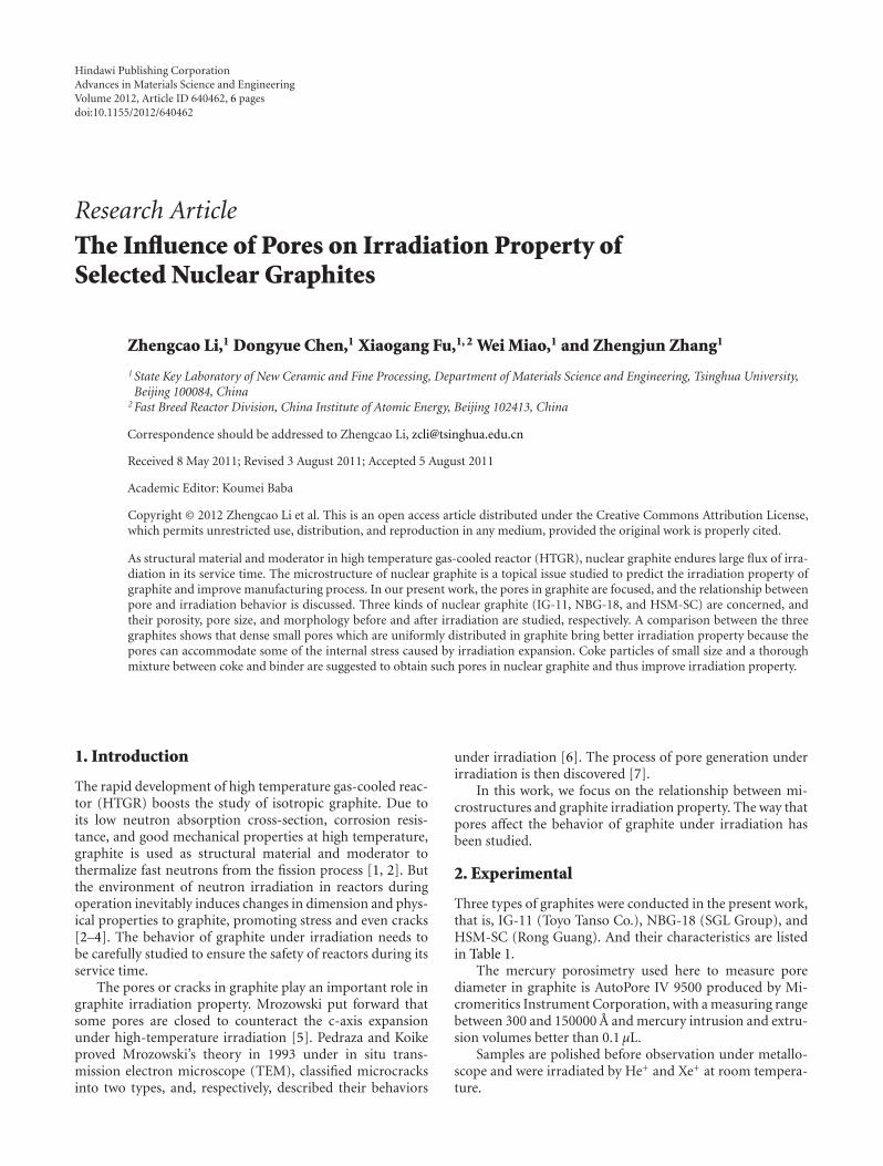
Hindawi Publishing CorporationAdvances in Materials Science and EngineeringVolume 2012, Article ID 640462, 6 pagesdoi:10.1155/2012/640462
Research Article
The Influence of Pores on Irradiation Property ofSelected Nuclear Graphites
Zhengcao Li,1 Dongyue Chen,1 Xiaogang Fu,1, 2 Wei Miao,1 and Zhengjun Zhang1
1 State Key Laboratory of New Ceramic and Fine Processing, Department of Materials Science and Engineering, Tsinghua University,Beijing 100084, China
2 Fast Breed Reactor Division, China Institute of Atomic Energy, Beijing 102413, China
Correspondence should be addressed to Zhengcao Li, [email protected]
Received 8 May 2011; Revised 3 August 2011; Accepted 5 August 2011
Academic Editor: Koumei Baba
Copyright © 2012 Zhengcao Li et al. This is an open access article distributed under the Creative Commons Attribution License,which permits unrestricted use, distribution, and reproduction in any medium, provided the original work is properly cited.
As structural material and moderator in high temperature gas-cooled reactor (HTGR), nuclear graphite endures large flux of irra-diation in its service time. The microstructure of nuclear graphite is a topical issue studied to predict the irradiation property ofgraphite and improve manufacturing process. In our present work, the pores in graphite are focused, and the relationship betweenpore and irradiation behavior is discussed. Three kinds of nuclear graphite (IG-11, NBG-18, and HSM-SC) are concerned, andtheir porosity, pore size, and morphology before and after irradiation are studied, respectively. A comparison between the threegraphites shows that dense small pores which are uniformly distributed in graphite bring better irradiation property because thepores can accommodate some of the internal stress caused by irradiation expansion. Coke particles of small size and a thoroughmixture between coke and binder are suggested to obtain such pores in nuclear graphite and thus improve irradiation property.
1. Introduction
The rapid development of high temperature gas-cooled reac-tor (HTGR) boosts the study of isotropic graphite. Due toits low neutron absorption cross-section, corrosion resis-tance, and good mechanical properties at high temperature,graphite is used as structural material and moderator tothermalize fast neutrons from the fission process [1, 2]. Butthe environment of neutron irradiation in reactors duringoperation inevitably induces changes in dimension and phys-ical properties to graphite, promoting stress and even cracks[2–4]. The behavior of graphite under irradiation needs tobe carefully studied to ensure the safety of reactors during itsservice time.
The pores or cracks in graphite play an important role ingraphite irradiation property. Mrozowski put forward thatsome pores are closed to counteract the c-axis expansionunder high-temperature irradiation [5]. Pedraza and Koikeproved Mrozowski’s theory in 1993 under in situ trans-mission electron microscope (TEM), classified microcracksinto two types, and, respectively, described their behaviors
under irradiation [6]. The process of pore generation underirradiation is then discovered [7].
In this work, we focus on the relationship between mi-crostructures and graphite irradiation property. The way thatpores affect the behavior of graphite under irradiation hasbeen studied.
2. Experimental
Three types of graphites were conducted in the present work,that is, IG-11 (Toyo Tanso Co.), NBG-18 (SGL Group), andHSM-SC (Rong Guang). And their characteristics are listedin Table 1.
The mercury porosimetry used here to measure porediameter in graphite is AutoPore IV 9500 produced by Mi-cromeritics Instrument Corporation, with a measuring rangebetween 300 and 150000 A and mercury intrusion and extru-sion volumes better than 0.1 μL.
Samples are polished before observation under metallo-scope and were irradiated by He+ and Xe+ at room tempera-ture.

2 Advances in Materials Science and Engineering
Table 1: Characteristics of three nuclear graphites chosen for thepresent study.
IG-11 NBG-18 HSM-SC
Coke Petrol coke Pitch coke Petrol coke
Average cokediameter (μm)
20 300 25
CompactionIsostatic
compactionVibratory
compactionIsostatic
compaction
Table 2: The apparent density and porosity of the three graphitesamples.
IG-11 NBG-18 HSM-SC
Apparent density (g/cm3) 1.77 1.86 1.84
Porosity (%) 20.8 17.3 18.2
3. Results and Discussion
3.1. Porosity. The total porosity of graphite can be calculatedby the following simple equation [8]:
ε =(
1− dV2.25
)× 100%, (1)
where dV is the apparent density of graphite, and2.25 (g/cm3) is the theoretical density of single-crystal graph-ite. Table 2 shows the calculation results of the three graphitesamples. They share similar porosity around 20%.
To further understand the distribution of pores in graph-ite, both mercury porosimetry and metalloscope are used.Figure 1 illustrates the distribution of pore diameters of thethree samples. The pores in IG-11 are small, with pore diam-eters mainly around 1. 5∼3 μm, whereas pores in HSM-SChave a sharp peak of 2∼4 μm, just a little bigger than IG-11. NBG-18 is quite different from both IG-11 and HSM-SC,with pore diameters scattered in a wide range of 5∼35 μm,and has a gradual rise around 25 μm. In other words, thoughsharing quite similar total porosity, NBG-18 has pores muchlarger than IG-11 or HSM-SC.
A parallel result could be drawn from the metalloscopeimages of the samples, shown in Figure 2. The morphologyof pores in IG-11 and HSM-SC is quite the same, both smallin size and large in quantity, whereas the pores in NBG-18 areapparently bigger and sparsely spread, reaching a diameter ofseveral tens of microns and even more.
Moreover, the pore difference between IG-11 and HSM-SC should also be noted, shown in Figure 3. The small sizepores are not uniformly distributed in HSM-SC, whichmeans that in some areas of HSM-SC, pores tend to appeartogether and form a sort of pore clusters (Figure 3(c)), whilein some other areas, only a few pores could be observed(Figure 3(d)). Pores in IG-11 are distributed much moreuniformly and evenly than in HSM-SC.
The nonuniform pore distribution of HSM-SC could alsobe illustrated by counting the aberrantly large pores ongraphite surface. In the 12× 21 mm2 surface area of graphitesample, IG-11 has 14 pores with diameters larger than
4096
8192
1638
4
3276
8
6553
6
1310
72
2621
44
5242
88
0
0.05
0.1
0.15
0.2
0.25
0.3
0.35
NBG-18
HSM-SC
Pore
volu
me
per
cen
tage
(%)
Pore diameter (A)
IG-11
Figure 1: Pore diameter distribution of the graphite samples.
100μm
(a)
(a)
100μm
(b)
(b)
100μm
(c)
(c)
Figure 2: Morphology of graphite samples before irradiation. (a)IG-11, (b) NBG-18, and (c) HSM-SC.
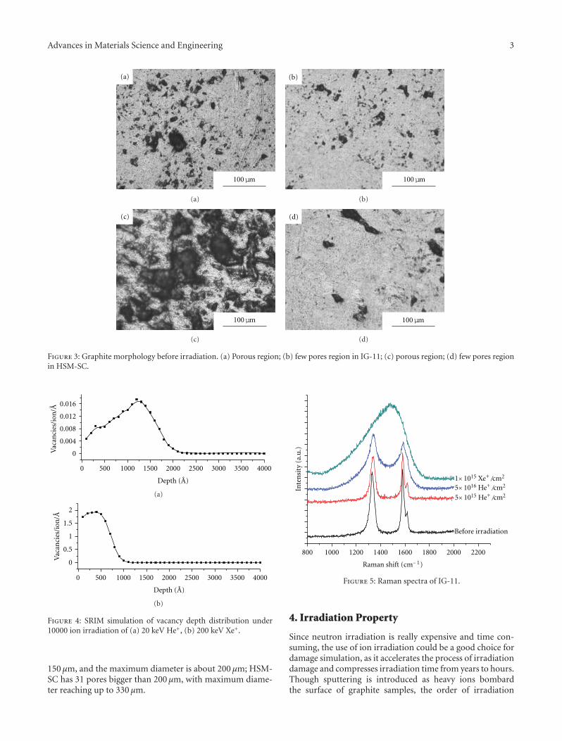
Advances in Materials Science and Engineering 3
100μm
(a)
(a)
100μm
(b)
(b)
100μm
(c)
(c)
100μm
(d)
(d)
Figure 3: Graphite morphology before irradiation. (a) Porous region; (b) few pores region in IG-11; (c) porous region; (d) few pores regionin HSM-SC.
0 500 1000 1500 2000 2500 3000 3500 4000
0
0.004
0.008
0.012
0.016
Vac
anci
es/i
on/A
Depth (A)
(a)
0 500 1000 1500 2000 2500 3000 3500 4000
Vac
anci
es/i
on/A
Depth (A)
0
0.5
1
1.5
2
(b)
Figure 4: SRIM simulation of vacancy depth distribution under10000 ion irradiation of (a) 20 keV He+, (b) 200 keV Xe+.
150 μm, and the maximum diameter is about 200 μm; HSM-SC has 31 pores bigger than 200 μm, with maximum diame-ter reaching up to 330 μm.
800 1000 1200 1400 1600 1800 2000 2200
Raman shift (cm− 1)
Before irradiation
1× 10¹⁵ Xe+/cm2
5× 10¹⁶ He+/cm2
5× 10¹⁵ He+/cm2
Inte
nsi
ty(a
.u.)
Figure 5: Raman spectra of IG-11.
4. Irradiation Property
Since neutron irradiation is really expensive and time con-suming, the use of ion irradiation could be a good choice fordamage simulation, as it accelerates the process of irradiationdamage and compresses irradiation time from years to hours.Though sputtering is introduced as heavy ions bombardthe surface of graphite samples, the order of irradiation

4 Advances in Materials Science and Engineering
100μm
(a)
100μm
(b)
100μm
(c)
100μm
(d)
100μm
(e)
100μm
(f)
Figure 6: Graphite morphology before and after 20 keV He+ irradiation with flux of 5 × 10¹⁶ ions/cm2. (a) IG-11, (c) NBG18, and (e)HSM-SC before irradiation; (b) IG-11, (d) NBG18, and (f) HSM-SC after irradiation.
properties of the three samples could still be determined bytheir morphology, as long as they are irradiated under thesame condition. Since the damage induced by 20 keV He+
irradiation is found to be quite light in our experiment, theXe+ irradiation, the kind of heavy ion irradiation which iscommonly used to study irradiation defects, is also intro-duced in the present work [9–11].
Software SRIM 2008 (stopping and range of ions in mat-ter 2008) can calculate the depth distribution of vacanciesthat ion irradiation may cause in selected material [12], andit is applied here to simulate He+ and Xe+ irradiation, shownin Figure 4. The defects brought by He+ and Xe+ irradiationare just near sample surface, and thus the surface structurechange can be detected by Raman measurements, since theeffective penetration depth of laser light is calculated to beabout 175 nm in our experiment.
There are three peaks in the Raman spectra of unir-radiated graphite: 1355 cm−1, 1580 cm−1
, and 1620 cm−1.1580 cm−1 peak (G-peak) is the characteristic peak of graph-ite, while 1620 cm−1 peak represents point defects in graph-ite, and 1355 cm−1 peak (D-peak) comes from defects andrandom orientation of grains in graphite [13]. After irradi-ation, the crystal structure of graphite surface is destroyed,resulting in the change of phonon-vibrating frequency, andthus the broadening and even overlapping of G-peak andD-peak in Raman spectra.
Figure 5 shows the Raman spectra of IG-11 before andafter ion irradiation. No specific change is observed after20 keV He+ irradiation at flux of 5 × 10¹⁵ ions/cm2, butG-peak and D-peak are both broadened if flux is increasedto 5 × 10¹⁶ ions/cm2, showing that defects in graph-ite are generated due to the large flux of He+ irradiation.
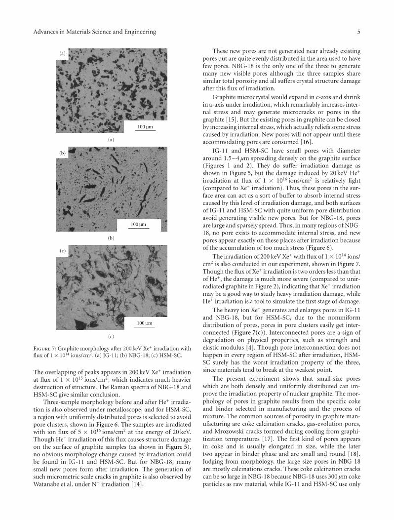
Advances in Materials Science and Engineering 5
100μm
(a)
(a)
100μm
(b)
(b)
100μm
(c)
(c)
Figure 7: Graphite morphology after 200 keV Xe+ irradiation withflux of 1 × 10¹⁴ ions/cm2. (a) IG-11; (b) NBG-18; (c) HSM-SC.
The overlapping of peaks appears in 200 keV Xe+ irradiationat flux of 1 × 10¹⁵ ions/cm2, which indicates much heavierdestruction of structure. The Raman spectra of NBG-18 andHSM-SC give similar conclusion.
Three-sample morphology before and after He+ irradia-tion is also observed under metalloscope, and for HSM-SC,a region with uniformly distributed pores is selected to avoidpore clusters, shown in Figure 6. The samples are irradiatedwith ion flux of 5 × 10¹⁶ ions/cm2 at the energy of 20 keV.Though He+ irradiation of this flux causes structure damageon the surface of graphite samples (as shown in Figure 5),no obvious morphology change caused by irradiation couldbe found in IG-11 and HSM-SC. But for NBG-18, manysmall new pores form after irradiation. The generation ofsuch micrometric scale cracks in graphite is also observed byWatanabe et al. under N+ irradiation [14].
These new pores are not generated near already existingpores but are quite evenly distributed in the area used to havefew pores. NBG-18 is the only one of the three to generatemany new visible pores although the three samples sharesimilar total porosity and all suffers crystal structure damageafter this flux of irradiation.
Graphite microcrystal would expand in c-axis and shrinkin a-axis under irradiation, which remarkably increases inter-nal stress and may generate microcracks or pores in thegraphite [15]. But the existing pores in graphite can be closedby increasing internal stress, which actually reliefs some stresscaused by irradiation. New pores will not appear until theseaccommodating pores are consumed [16].
IG-11 and HSM-SC have small pores with diameteraround 1.5∼4 μm spreading densely on the graphite surface(Figures 1 and 2). They do suffer irradiation damage asshown in Figure 5, but the damage induced by 20 keV He+
irradiation at flux of 1 × 10¹⁶ ions/cm2 is relatively light(compared to Xe+ irradiation). Thus, these pores in the sur-face area can act as a sort of buffer to absorb internal stresscaused by this level of irradiation damage, and both surfacesof IG-11 and HSM-SC with quite uniform pore distributionavoid generating visible new pores. But for NBG-18, poresare large and sparsely spread. Thus, in many regions of NBG-18, no pore exists to accommodate internal stress, and newpores appear exactly on these places after irradiation becauseof the accumulation of too much stress (Figure 6).
The irradiation of 200 keV Xe+ with flux of 1× 10¹⁴ ions/cm2 is also conducted in our experiment, shown in Figure 7.Though the flux of Xe+ irradiation is two orders less than thatof He+, the damage is much more severe (compared to unir-radiated graphite in Figure 2), indicating that Xe+ irradiationmay be a good way to study heavy irradiation damage, whileHe+ irradiation is a tool to simulate the first stage of damage.
The heavy ion Xe+ generates and enlarges pores in IG-11and NBG-18, but for HSM-SC, due to the nonuniformdistribution of pores, pores in pore clusters easily get inter-connected (Figure 7(c)). Interconnected pores are a sign ofdegradation on physical properties, such as strength andelastic modulus [4]. Though pore interconnection does nothappen in every region of HSM-SC after irradiation, HSM-SC surely has the worst irradiation property of the three,since materials tend to break at the weakest point.
The present experiment shows that small-size poreswhich are both densely and uniformly distributed can im-prove the irradiation property of nuclear graphite. The mor-phology of pores in graphite results from the specific cokeand binder selected in manufacturing and the process ofmixture. The common sources of porosity in graphite man-ufacturing are coke calcination cracks, gas-evolution pores,and Mrozowski cracks formed during cooling from graphi-tization temperatures [17]. The first kind of pores appearsin coke and is usually elongated in size, while the latertwo appear in binder phase and are small and round [18].Judging from morphology, the large-size pores in NBG-18are mostly calcinations cracks. These coke calcination crackscan be so large in NBG-18 because NBG-18 uses 300 μm cokeparticles as raw material, while IG-11 and HSM-SC use only

6 Advances in Materials Science and Engineering
20 or 25 μm coke particles which cannot contain such bigcalcination cracks (Table 2).
Similarly, since coke and binder phase contain pores ofdifferent size and morphology, a heterogeneous mixture ofthem may lead to the nonuniform pore distribution in HSM-SC. Japanese researchers lay emphasis on the importanceof a fine and homogeneous structure in isotropic graphitemanufacturing and admit that their use of small-size cokeparticles makes it difficult to mix coke and pitch binder well[19], which is also the case for HSM-SC.
5. Conclusion
The way that pores affect irradiation property of nucleargraphite has been studied in the present work through He+
and Xe+ irradiation. Dense small pores which are uniformlyspread in graphite bring better irradiation property becausethe pores can accommodate some of the internal stresscaused by irradiation expansion. And the use of small-sizecoke particles and a thorough mixture of coke and pitch canhelp obtain such small dense pores in nuclear graphite andthus improve irradiation property.
Acknowledgments
The authors are grateful to have the financial support of theNational Natural Science Foundation of China (61076003)and the National Basic Research Program of China (973 pro-gram, 2010CB731600 and 2010CB832900).
References
[1] E. L. Fuller and J. M. Okoh, “Kinetics and mechanisms of thereaction of air with nuclear grade graphites: IG-110,” Journal ofNuclear Materials, vol. 240, no. 3, pp. 241–250, 1997.
[2] Y. S. Lim, S. H. Chi, and K. Y. Cho, “Change of properties afteroxidation of IG-11 graphite by air and CO2 gas,” Journal ofNuclear Materials, vol. 374, no. 1-2, pp. 123–128, 2008.
[3] L. Babout, P. M. Mummery, T. J. Marrow, A. Tzelepi, and P.J. Withers, “The effect of thermal oxidation on polycrystallinegraphite studied by X-ray tomography,” Carbon, vol. 43, no. 4,pp. 765–774, 2005.
[4] G. B. Neighbour and P. J. Hacker, “The variation of com-pressive strength of AGR moderator graphite with increasingthermal weight loss,” Materials Letters, vol. 51, no. 4, pp. 307–314, 2001.
[5] S. Mrozowski, Proceedings of the First and Second Conferenceson Carbon, University of Buffalo, New York, NY, USA, 1956.
[6] D. F. Pedraza and J. Koike, “Dimensional changes in grade H-451 nuclear graphite due to electron irradiation,” Carbon, vol.32, no. 4, pp. 727–734, 1994.
[7] G. B. Neighbour, “Modelling of dimensional changes in irra-diated nuclear graphites,” Journal of Physics D, vol. 33, no. 22,pp. 2966–2972, 2000.
[8] S. H. Chi and G. C. Kim, “Comparison of 3 MeV C+ ion-irradiation effects between the nuclear graphites made of pitchand petroleum cokes,” Journal of Nuclear Materials, vol. 381,no. 1-2, pp. 98–105, 2008.
[9] Z. C. Li, D. P. Yu, and B. X. Liu, “Manipulation of orderedlayered structures by interface-assisted ion-beam mixing inimmiscible Ag-Co and Ag-Ni systems,” Physical Review B, vol.65, no. 24, Article ID 245403, 2002.
[10] Y. Hu, Z. C. Li, and Z. J. Zhang, “Irradiation induced localizedamorphization in Mo-Re alloy films,” Materials Transactions,vol. 51, no. 4, pp. 670–674, 2010.
[11] Y. Hu, Z. C. Li, and Z. J. Zhang, “Ion-implantation-inducedpatterns formation on silicon substrates,” Physica E, vol. 41,no. 5, pp. 833–837, 2009.
[12] Z. C. Li, H. Abe, and N. Sekimura, “Detection of point defectsupon ion irradiation by means of precipitate coherency,” Jour-nal of Nuclear Materials, vol. 362, no. 1, pp. 87–92, 2007.
[13] H. W. Willes and M. Roberto, Raman Scattering in MaterialScience, Springer, New York, NY, USA, 2000.
[14] H. Watanabe, K. Takahashi, and M. Iwaki, “Structural charac-terization of ion implanted pyrolytic graphite,” Nuclear Instru-ments and Methods in Physics Research B, vol. 257, no. 1-2, pp.549–553, 2007.
[15] D. K. L. Tsang and B. J. Marsden, “Effects of dimensionalchange strain in nuclear graphite component stress analysis,”Nuclear Engineering and Design, vol. 237, no. 9, pp. 897–904,2007.
[16] M. R. Bradford and A. G. Steer, “A structurally-based modelof irradiated graphite properties,” Journal of Nuclear Materials,vol. 381, no. 1-2, pp. 137–144, 2008.
[17] G. Hall, B. J. Marsden, and S. L. Fok, “The microstructuralmodelling of nuclear grade graphite,” Journal of Nuclear Mate-rials, vol. 353, no. 1-2, pp. 12–18, 2006.
[18] K. Y. Wen, T. J. Marrow, and B. J. Marsden, “The microstruc-ture of nuclear graphite binders,” Carbon, vol. 46, no. 1, pp.62–71, 2008.
[19] The Carbon Society of Japan, “Elementary course to new car-bon materials, Specialized Commission of Carbon Materialsunder the Chinese Metal Society trans & edit,” 1999.

Hindawi Publishing CorporationAdvances in Materials Science and EngineeringVolume 2012, Article ID 536853, 5 pagesdoi:10.1155/2012/536853
Research Article
Preparation and Properties of Ag-Containing Diamond-LikeCarbon Films by Magnetron Plasma Source Ion Implantation
K. Baba,1 R. Hatada,2 S. Flege,2 and W. Ensinger2
1 Industrial Technology Center of Nagasaki, Applied Technology Division, Omura, Nagasaki 856-0026, Japan2 Department of Materials Science, Technische Universitat Darmstadt, 64287 Darmstadt, Germany
Correspondence should be addressed to K. Baba, [email protected]
Received 27 April 2011; Revised 31 July 2011; Accepted 2 August 2011
Academic Editor: Robert G. Elliman
Copyright © 2012 K. Baba et al. This is an open access article distributed under the Creative Commons Attribution License, whichpermits unrestricted use, distribution, and reproduction in any medium, provided the original work is properly cited.
The doping effect of silver on the structure and properties of diamond-like carbon (DLC) films was investigated. The sampleswere prepared by a process combining acetylene plasma source ion implantation (high-voltage pulses of −10 kV) with reactivemagnetron sputtering of an Ag disc. A mixture of two gases, argon, and acetylene was introduced into the discharge chamber asworking gas for plasma formation. A negative high-voltage pulse was applied to the substrate holder, thus, accelerating ions towardsthe substrate. The chemical composition of the deposited films was modified by the respective gas flows and determined using X-ray photoelectron spectroscopy and secondary ion mass spectrometry. The silver concentration within the DLC films influencedthe structure and the tribological properties. The surface roughness, as observed by scanning electron microscopy, increased withsilver concentration. The film structure was characterized by Raman spectroscopy and X-ray diffractometry (XRD). The DLCfilms were mainly amorphous, containing crystalline silver, with the amount of silver depending on the process conditions. Thetribological properties of the films were improved by the silver doping. The lowest friction coefficient of around 0.06 was derivedat a low silver content.
1. Introduction
Plasma source ion implantation (PSII) is a simple buteffective ion implantation and deposition method for surfacemodification of materials [1–3]. In the PSII process, anegative high-voltage pulse is applied directly to a target, andthus a plasma is generated in front of the substrate. The ionsfrom the plasma forming gases such as nitrogen, oxygen, orhydrocarbons are implanted into the substrate surface. Thishas been reported to improve several parameters such ashardness, adhesion, friction coefficient, and wear properties[4–11].
Furthermore, it is possible to implant metal ions by PSIIor to deposit films. If PSII is combined with a conventionalsputtering process, the element sputtered from the targetdoes not only form a film on top of the substrate but is alsoimplanted into the substrate [12]. Hence, a mixed zone atthe interface is formed thereby improving the adhesion ofthe film. PSII can also be applied to deposit diamond-likecarbon (DLC) films, for example, by altering experimentalparameters such as the pulse voltage and length and by
using acetylene as working gas [9]. Here, the incorporationof other elements into the DLC films offers the possibilityto modify the properties of the DLC films. Again, thisis feasible by a combined process. Since both processes(sputtering and PSII) are run simultaneously in a singleexperimental chamber, a mixture of a hydrocarbon gasand argon has to be used. The argon ions are used tosputter material from the cathode whereas the hydrocarbonsfrom the plasma function as a source for deposition of aDLC film, resulting in a compound film [12, 13]. Metal-containing DLC films with properties intermediate betweenDLC and metal carbides have been shown to improvethe adhesion and hardness as well as the wear properties.This is due to the microstructure of the films comprisingnanocrystalline grains in an amorphous carbon matrix [14–16]. The incorporation of silver into DLC films (Ag-DLC) isof interest as it offers the possibility to reduce the internalstress [17], to enhance the wear properties [18], and becauseit provides films that are haemocompatible and antibacterial[19–21].

2 Advances in Materials Science and Engineering
ITCN 5 kV
100 nm
×80,000 13 mm
61.3 at.% Ag
(a)
ITCN 5 kV
100 nm
×80,000 13 mm
13.4 at.% Ag
(b)
ITCN 5 kV
100 nm
×80,000 13 mm
5.9 at.% Ag
(c)
ITCN 5 kV
100 nm
×80,000 13 mm
4.5 at.% Ag
(d)
ITCN 5 kV
100 nm
×80,000 14 mm
1.8 at.% Ag
(e)
Figure 1: SEM images of the surfaces of silver-containing DLC films.
In our previous works, we have reported on the plasmasource implantation of sputtered Ni ions into materialsand the effects of metal (Ti, Ta, Fe, Co, Ni, Mo, and W)incorporation into DLC films on the composition, structure,and phase formation [12, 13, 22]. In this study, the influenceof the silver content in DLC films prepared by a combinedmagnetron sputtering and PSII process on the structure,surface roughness, and tribological properties of the films isdiscussed.
2. Experimental
The silver containing Ag-DLC films were deposited on siliconwafer substrates (100) using a PSII method combined withmagnetron sputtering. Details of the magnetron plasmasource ion implantation apparatus used in this study aredescribed in detail elsewhere [22]. The base pressure in thechamber was 10−4 Pa. Argon and acetylene (C2H2) were letinto the vacuum chamber by controlling their flow throughmass flow controllers. The film composition was altered bychanging the flow rate of the acetylene gas between 2.1 and5.6 sccm while keeping the argon flow rate fixed at 20 sccm.The vacuum pressure during implantation was set to around1 Pa. An Ag disc with four inches (10 cm) in diameter wasused as the sputtering target. The plasma was generated bythe application of a 13.56 MHz, 150 W rf power to the mag-netron sputter source. A pulse voltage of −10 kV superposedto a DC voltage of −2 kV was applied to the substrate holderat a pulse repetition rate of 100 Hz and a pulse durationof 100 μs. The process times were between 0.2 and 1 h. The
thickness of the films was monitored by cross-sectional scan-ning electron microscopy (SEM) observation. The surfacemorphology of the films was also observed by SEM. Thechemical composition and chemical state of the films wereevaluated using X-ray photoelectron spectroscopy (XPS)under Mg Kα X-ray irradiation. Depth profiles were obtainedby secondary ion mass spectrometry using 3.5 keV O2
+ pri-mary ions detecting positive secondary ions. The structuralinformation was studied by X-ray diffractometry (XRD)with Θ–2Θ configuration and Raman spectroscopy with anexcitation wavelength of 514 nm of an argon ion laser.
A ball-on-disc type apparatus was employed for thetribological tests using balls of tungsten carbide with 6 mmdiameter. Friction coefficients were determined with a nor-mal load of 2 N and a velocity of 100 mm/s. The tests werecarried out at room temperature and at about 25% relativehumidity.
3. Results and Discussion
The silver content in the films depended on the volumefraction of C2H2 in the C2H2/Ar gas mixture. For thelowest flow rate of C2H2, a silver content of 61.3 at.% wasfound, as determined by XPS, with decreasing Ag contentfor increasing C2H2 flow rate, for example, 1.8 at.% Ag at3.5 sccm. The concentration of the metal in the DLC filmscould be controlled by changing the fraction of C2H2 inthe gases. Similar results were reported for W-containingDLC [13, 23]. The thicknesses of the films were 0.5–1 μm.The surface morphology as observed by SEM is shown inFigure 1. A very smooth structure was observed for the lower
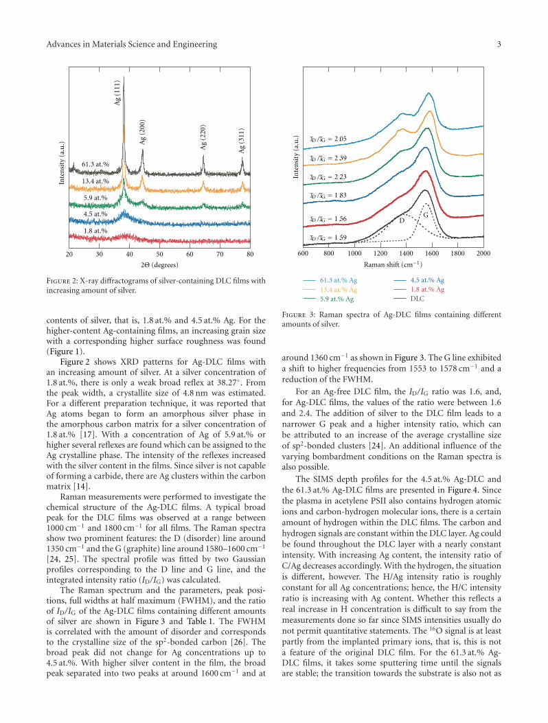
Advances in Materials Science and Engineering 3
Inte
nsi
ty(a
.u.)
20 30 40 50 60 70 80
13.4 at.%
5.9 at.%
4.5 at.%
1.8 at.%
61.3 at.%
Ag
(111
)
Ag
(200
)
Ag
(220
)
Ag
(311
)
2Θ (degrees)
Figure 2: X-ray diffractograms of silver-containing DLC films withincreasing amount of silver.
contents of silver, that is, 1.8 at.% and 4.5 at.% Ag. For thehigher-content Ag-containing films, an increasing grain sizewith a corresponding higher surface roughness was found(Figure 1).
Figure 2 shows XRD patterns for Ag-DLC films withan increasing amount of silver. At a silver concentration of1.8 at.%, there is only a weak broad reflex at 38.27◦. Fromthe peak width, a crystallite size of 4.8 nm was estimated.For a different preparation technique, it was reported thatAg atoms began to form an amorphous silver phase inthe amorphous carbon matrix for a silver concentration of1.8 at.% [17]. With a concentration of Ag of 5.9 at.% orhigher several reflexes are found which can be assigned to theAg crystalline phase. The intensity of the reflexes increasedwith the silver content in the films. Since silver is not capableof forming a carbide, there are Ag clusters within the carbonmatrix [14].
Raman measurements were performed to investigate thechemical structure of the Ag-DLC films. A typical broadpeak for the DLC films was observed at a range between1000 cm−1 and 1800 cm−1 for all films. The Raman spectrashow two prominent features: the D (disorder) line around1350 cm−1 and the G (graphite) line around 1580–1600 cm−1
[24, 25]. The spectral profile was fitted by two Gaussianprofiles corresponding to the D line and G line, and theintegrated intensity ratio (ID/IG) was calculated.
The Raman spectrum and the parameters, peak posi-tions, full widths at half maximum (FWHM), and the ratioof ID/IG of the Ag-DLC films containing different amountsof silver are shown in Figure 3 and Table 1. The FWHMis correlated with the amount of disorder and correspondsto the crystalline size of the sp2-bonded carbon [26]. Thebroad peak did not change for Ag concentrations up to4.5 at.%. With higher silver content in the film, the broadpeak separated into two peaks at around 1600 cm−1 and at
600 800 1000 1200 1400 1600 1800 2000
61.3 at.% Ag13.4 at.% Ag5.9 at.% Ag
4.5 at.% Ag1.8 at.% AgDLC
Inte
nsi
ty(a
.u.) ID/IG = 2.05
ID/IG = 2.39
ID/IG = 2.23
ID/IG = 1.83
ID/IG = 1.56
ID/IG = 1.59
DG
Raman shift (cm−1)
Figure 3: Raman spectra of Ag-DLC films containing differentamounts of silver.
around 1360 cm−1 as shown in Figure 3. The G line exhibiteda shift to higher frequencies from 1553 to 1578 cm−1 and areduction of the FWHM.
For an Ag-free DLC film, the ID/IG ratio was 1.6, and,for Ag-DLC films, the values of the ratio were between 1.6and 2.4. The addition of silver to the DLC film leads to anarrower G peak and a higher intensity ratio, which canbe attributed to an increase of the average crystalline sizeof sp2-bonded clusters [24]. An additional influence of thevarying bombardment conditions on the Raman spectra isalso possible.
The SIMS depth profiles for the 4.5 at.% Ag-DLC andthe 61.3 at.% Ag-DLC films are presented in Figure 4. Sincethe plasma in acetylene PSII also contains hydrogen atomicions and carbon-hydrogen molecular ions, there is a certainamount of hydrogen within the DLC films. The carbon andhydrogen signals are constant within the DLC layer. Ag couldbe found throughout the DLC layer with a nearly constantintensity. With increasing Ag content, the intensity ratio ofC/Ag decreases accordingly. With the hydrogen, the situationis different, however. The H/Ag intensity ratio is roughlyconstant for all Ag concentrations; hence, the H/C intensityratio is increasing with Ag content. Whether this reflects areal increase in H concentration is difficult to say from themeasurements done so far since SIMS intensities usually donot permit quantitative statements. The 16O signal is at leastpartly from the implanted primary ions, that is, this is nota feature of the original DLC film. For the 61.3 at.% Ag-DLC films, it takes some sputtering time until the signalsare stable; the transition towards the substrate is also not as

4 Advances in Materials Science and Engineering
Table 1: Raman spectroscopy data of Ag-DLC films with various amounts of silver.
Sample No. C2H2 flow rate Deposition rate(nm/min)
Ag concentration(at.%)
G band peak(cm−1)
FWHM(cm−1)
ID/IG
1 2.10 39.5 61.3 1578.6 111.0 2.05
2 1.75 15.3 32.5 1588.2 115.0 2.26
3 2.80 13.2 13.4 1584.0 113.1 2.39
4 3.15 9.4 5.9 1566.3 129.7 2.23
5 3.50 13.4 4.5 1555.5 144.9 1.83
6 3.50 16.0 1.8 1557.0 151.8 1.56
7 5.60 21.6 0 1553.6 153.6 1.59
Sputtering time (s)
Inte
nsi
ty(c
oun
ts/s
)
100
102
104
106
108
0 500 1000 1500 2000 2500
107Ag 109Ag
1H12C
28Si
16O
30Si
18O
(a)
Sputtering time (s)
Inte
nsi
ty(c
oun
ts/s
)
100
102
104
106
108
0 500 1000 1500 2000
107Ag 109Ag
1H 12C
28Si16O
30Si
18O
(b)
Figure 4: Secondary ion mass spectrometry depth profiles of (a)4.5 at.% silver and (b) 61.3 at.% silver-incorporated DLC films.
sharp as in the case of the other profile. This is due to themuch higher surface roughness of the Ag-rich sample (seeFigure 1).
Figure 5 shows the results of the ball-on-disc tests in dryconditions for the Ag-free film and several Ag containingfilms. A small addition of silver decreased the friction
Number of rotations
Fric
tion
coe
cien
t
13.4 at.% Ag5.9 at.% Ag4.5 at.% Ag
1.8 at.% AgDLC
0
0.1
0.2
0.3
0.4
0.5
0.6
0 1000 2000 3000 4000 5000 6000 7000 8000
Figure 5: Friction coefficient as a function of rotations in the ball-on-disk tests of silver-containing DLC films.
coefficient as compared to the Ag-free film. With higherconcentrations of silver, the friction coefficient increasedfrom 0.06 to 0.28 with increasing Ag concentration in thefilm. With the 1.8 at.% Ag-DLC film, the friction coefficientwas around 0.06 at the beginning of the test, and stablefor several thousand rotations. The surface of this filmwas relatively smooth, and section profiles of the slidingtraces of this film after the wear test showed only a veryfine wear track. Choi et al. [17] reported the existence ofamorphous silver phase precipitates with a size of 2 nm inthe amorphous carbon matrix from transmission electronmicroscopy. In this study, XRD measurement suggested acomposite structure of nanocrystalline Ag/amorphous DLCfor the 1.8 at.% Ag-containing film. So the tribologicalbehavior can be improved by silver addition to the film,which can be attributed to the nanoscale grain size structureof the film. This is also valid for higher Ag contents [18].
4. Conclusions
Silver-containing DLC films were successfully prepared bya process combining reactive magnetron sputtering with

Advances in Materials Science and Engineering 5
plasma source ion implantation. The content of silver in theDLC films could be controlled by setting the flow rates of theinvolved argon and acetylene gases. Silver atoms were incor-porated over the whole depth of the DLC films, but tendedto agglomerate. The structure and tribological propertieswere affected by the Ag content of the DLC films. The DLCstructure of the films changed with deposition conditions asseen by the Raman spectra (separation of one broad peakinto two peaks for the silver-containing DLC films). Thesurface roughness increased with the silver content in thefilms. The best wear property was derived for the 1.8 at.%silver-containing DLC film and showed an improvementas compared to the Ag-free film. Investigations about theantibacterial activity for use in biological applications areunderway and will be presented elsewhere.
References
[1] J. R. Conrad and T. Castagna, “Plasma Source Ion Implan-tation for Surface Modification,” Bulletin of the AmericanPhysical Society, vol. 31, p. 1429, 1986.
[2] J. R. Conrad, “Sheath thickness and potential profiles ofion-matrix sheaths for cylindrical and spherical electrodes,”Journal of Applied Physics, vol. 62, no. 3, pp. 777–779, 1987.
[3] J. Tendys, I. J. Donnelly, M. J. Kenny, and J. T. A. Pollock,“Plasma immersion ion implantation using plasmas generatedby radio frequency techniques,” Applied Physics Letters, vol. 53,no. 22, pp. 2143–2145, 1988.
[4] K. C. Walter, R. A. Dood, and J. R. Conrad, “Corrosion behav-ior of nitrogen implanted aluminum,” Nuclear Instrumentsand Methods in Physics Research Section B, vol. 106, no. 1–4,pp. 522–526, 1995.
[5] A. Chen, X. Qiu, K. Sridharan et al., “Chromium plating pol-lution source reduction by plasma source ion implantation,”Surface and Coatings Technology, vol. 82, no. 3, pp. 305–310,1996.
[6] B. Y. Tang, P. K. Chu, S. Y. Wang, K. W. Chow, and X. F. Wang,“Methane and nitrogen plasma immersion ion implantationof titanium metal,” Surface and Coatings Technology, vol. 103-104, pp. 248–251, 1998.
[7] S. Han, H. Kim, Y. Lee, J. Lee, and S.-G. Kim, “Plasma sourceion implantation of nitrogen, carbon and oxygen into Ti-6A1-4V alloy,” Surface and Coatings Technology, vol. 82, no. 3, pp.270–276, 1996.
[8] K. C. Walter, M. Nastasi, N. P. Baker et al., “Advances in PSIItechniques for surface modification,” Surface and CoatingsTechnology, vol. 103-104, no. 1, pp. 205–211, 1998.
[9] K. Baba and R. Hatada, “Deposition of diamond-like carbonfilms on polymers by plasma source ion implantation,” ThinSolid Films, vol. 506-507, pp. 55–58, 2006.
[10] J. Chen, J. Blanchard, J. R. Conrad, and R. A. Dodd, “Structureand wear properties of carbon implanted 304 stainless steelusing plasma source ion implantation,” Surface and CoatingsTechnology, vol. 53, no. 3, pp. 267–274, 1992.
[11] J. Chen, J. R. Conrad, and R. A. Dodd, “Methane plasmasource ion implantation (PSII) for improvement of tribolog-ical and corrosion properties,” Journal of Materials ProcessingTechnology, vol. 49, no. 1-2, pp. 115–124, 1995.
[12] K. Baba and R. Hatada, “Preparation and properties of metal-containing diamond-like carbon films by magnetron plasmasource ion implantation,” Surface and Coatings Technology,vol. 196, no. 1–3, pp. 207–210, 2005.
[13] K. Baba and R. Hatada, “Preparation and properties of metalcontaining diamond-like carbon films by magnetron plasmasource ion implantation,” Surface and Coatings Technology,vol. 158-159, pp. 373–376, 2002.
[14] C. P. Klages and R. Memming, “Microstructure and physicalproperties of metal-containing hydrogenated carbon films,”Materials Science Forum, vol. 52-53, p. 609, 1990.
[15] C. Donnet, “Recent progress on the tribology of dopeddiamond-like and carbon alloy coatings: a review,” Surface andCoatings Technology, vol. 100-101, no. 1–3, pp. 180–186, 1998.
[16] A. A. Voevodin, S. V. Prasad, and J. S. Zabinski, “Nanocrys-talline carbide/amorphous carbon composites,” Journal ofApplied Physics, vol. 82, no. 2, pp. 855–858, 1997.
[17] H. W. Choi, J. H. Choi, K. R. Lee, J. P. Ahn, and K. H.Oh, “Structure and mechanical properties of Ag-incorporatedDLC films prepared by a hybrid ion beam deposition system,”Thin Solid Films, vol. 516, no. 2–4, pp. 248–251, 2007.
[18] C. P. Lungu, I. Mustata, G. Musa et al., “Formation ofnanostructured Re-Cr-Ni diffusion barrier coatings on Nbsuperalloys by TVA method,” Surface and Coatings Technology,vol. 200, no. 1-4, pp. 399–402, 2005.
[19] J. L. Endrino, R. E. Galindo, H.-S. Zhang et al., “Structureand properties of silver-containing a-C(H) films deposited byplasma immersion ion implantation,” Surface and CoatingsTechnology, vol. 202, no. 15, pp. 3675–3682, 2008.
[20] H. W. Choi, R. H. Dauskardt, S.-C. Lee, K. R. Lee, J. P.Ahn, and K. H. Oh, “Characteristic of silver doped DLC filmson surface properties and protein adsorption,” Diamond andRelated Materials, vol. 17, no. 3, pp. 252–257, 2008.
[21] J. Wang, N. Huang, C. J. Pan et al., “Bacterial repellencefrom polyethylene terephthalate surface modified by acetyleneplasma immersion ion implantation—deposition,” Surfaceand Coatings Technology, vol. 186, no. 1-2, pp. 299–304, 2004.
[22] K. Baba and R. Hatada, “Deposition and characterization ofTi- and W-containing diamond-like carbon films by plasmasource ion implantation,” Surface and Coatings Technology,vol. 169-170, pp. 287–290, 2003.
[23] A.-Y. Wang, K.-R. Lee, J.-P. Ahn, and J. H. Han, “Structureand mechanical properties of W incorporated diamond-likecarbon films prepared by a hybrid ion beam depositiontechnique,” Carbon, vol. 44, no. 9, pp. 1826–1832, 2006.
[24] J. Robertson, “Diamond-like amorphous carbon,” MaterialsScience and Engineering, vol. 37, pp. 129–281, 2002.
[25] A. C. Ferrari and J. Robertson, “Interpretation of Ramanspectra of disordered and amorphous carbon,” Physical ReviewB, vol. 61, no. 20, pp. 14095–14107, 2000.
[26] C. Casiraghi, A. C. Ferrari, and J. Robertson, “Ramanspectroscopy of hydrogenated amorphous carbons,” PhysicalReview B, vol. 72, Article ID 085401, 14 pages, 2005.

Hindawi Publishing CorporationAdvances in Materials Science and EngineeringVolume 2012, Article ID 841961, 6 pagesdoi:10.1155/2012/841961
Review Article
Focused Ion Beam in the Study of Biomaterialsand Biological Matter
Kathryn Grandfield and Hakan Engqvist
Department of Engineering Sciences, The Angstrom Laboratory, Uppsala University, Uppsala 751 21, Sweden
Correspondence should be addressed to Kathryn Grandfield, [email protected]
Received 20 April 2011; Accepted 20 June 2011
Academic Editor: David D. Cohen
Copyright © 2012 K. Grandfield and H. Engqvist. This is an open access article distributed under the Creative CommonsAttribution License, which permits unrestricted use, distribution, and reproduction in any medium, provided the original work isproperly cited.
The application of focused ion beam (FIB) techniques in the life sciences has progressed by leaps and bounds over the past decade.A once dedicated ion beam instrument, the focused ion beam today is generally coupled with a plethora of complementary toolssuch as dual-beam scanning electron microscopy (SEM), environmental SEM, energy dispersive X-ray spectroscopy (EDX), orcryogenic possibilities. All of these additions have contributed to the advancement of focused ion beam use in the study ofbiomaterials and biological matter. Biomaterials, cells, and their interfaces can be routinely imaged, analyzed, or prepared fortechniques such as transmission electron microscopy (TEM) with this comprehensive tool. Herein, we review the uses, advances,and challenges associated with the application of FIB techniques to the life sciences, with particular emphasis on TEM preparationof biomaterials, biological matter, and their interfaces using FIB.
1. Challenges with Biological Samples
Analyzing cellular and biological structures at high reso-lution remains a challenge due to the nature of biologicalmaterials and their interaction with electron and ion beams.Nonconductive samples simply result in charging, whichlimits the ability to image them with ease or high quality.Besides the use of an environmental chamber, solutions existto mediate these problems.
Primarily, a sequence of sample preparation steps aids inthe reduction of artefacts associated with biological matter.The fixation, dehydration, and embedding of samples are astandard protocol for many researchers. Indeed, these meth-ods present potential drawbacks. Firstly, it is unclear howmuch of the original structure is altered after preservationtechniques. The penetration of chemical fixatives such as al-dehydes and osmium tetroxide indeed influences the chem-ical make-up of the sample as a whole. On the other hand,the addition of heavy elements such as osmium throughOTOTO (osmium tetroxde/thiocarbohydrazide/osmium tet-roxide/thiocarbohydrazide/osmium tetroxide) conductivestaining has been shown to lead to a reduction in charging
artefacts, simplifying the imaging process [1, 2]. Neverthe-less, subsequent embedding steps are associated with slightsample heating and shrinkage, which may alter natural struc-tures. In addition, the cutting and grinding of embeddedspecimens may introduce additional damage to surfaces ana-lyzed. In the case of biomaterials in contact with tissues thereexists a so-called hybrid interface of soft and hard materialsin contact. Embedding and sectioning techniques may resultin the elimination of interfacial contact. Palmquist et al. havefurthermore demonstrated that the choice of embeddingresin has an effect on the overall shrinkage and separationof the specimen [3]. Nevertheless, in some cases, embeddingof biological samples has been proven to yield higher qualityresults, such as improved imaging of subcellular componentsversus critical-point dried samples, which tend to yield betterinformation regarding external cellular structures [2].
To circumvent the artefacts that may be associated withconventional fixative preparation methods, a cyrogenic(cryo-) approach may be taken. Modern focused ion beamsystems are implementing cryostages and transfer devicesto eliminate the preservation steps usually required forbiological specimens. In this regard, the true, unaltered
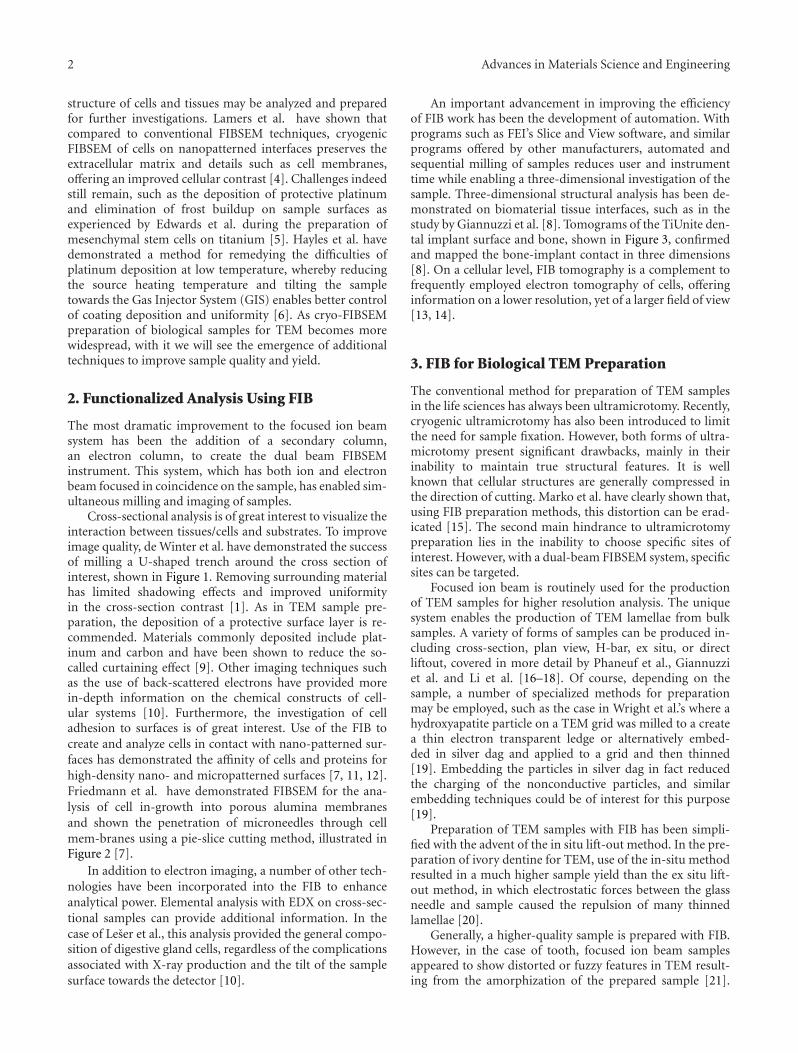
2 Advances in Materials Science and Engineering
structure of cells and tissues may be analyzed and preparedfor further investigations. Lamers et al. have shown thatcompared to conventional FIBSEM techniques, cryogenicFIBSEM of cells on nanopatterned interfaces preserves theextracellular matrix and details such as cell membranes,offering an improved cellular contrast [4]. Challenges indeedstill remain, such as the deposition of protective platinumand elimination of frost buildup on sample surfaces asexperienced by Edwards et al. during the preparation ofmesenchymal stem cells on titanium [5]. Hayles et al. havedemonstrated a method for remedying the difficulties ofplatinum deposition at low temperature, whereby reducingthe source heating temperature and tilting the sampletowards the Gas Injector System (GIS) enables better controlof coating deposition and uniformity [6]. As cryo-FIBSEMpreparation of biological samples for TEM becomes morewidespread, with it we will see the emergence of additionaltechniques to improve sample quality and yield.
2. Functionalized Analysis Using FIB
The most dramatic improvement to the focused ion beamsystem has been the addition of a secondary column,an electron column, to create the dual beam FIBSEMinstrument. This system, which has both ion and electronbeam focused in coincidence on the sample, has enabled sim-ultaneous milling and imaging of samples.
Cross-sectional analysis is of great interest to visualize theinteraction between tissues/cells and substrates. To improveimage quality, de Winter et al. have demonstrated the successof milling a U-shaped trench around the cross section ofinterest, shown in Figure 1. Removing surrounding materialhas limited shadowing effects and improved uniformityin the cross-section contrast [1]. As in TEM sample pre-paration, the deposition of a protective surface layer is re-commended. Materials commonly deposited include plat-inum and carbon and have been shown to reduce the so-called curtaining effect [9]. Other imaging techniques suchas the use of back-scattered electrons have provided morein-depth information on the chemical constructs of cell-ular systems [10]. Furthermore, the investigation of celladhesion to surfaces is of great interest. Use of the FIB tocreate and analyze cells in contact with nano-patterned sur-faces has demonstrated the affinity of cells and proteins forhigh-density nano- and micropatterned surfaces [7, 11, 12].Friedmann et al. have demonstrated FIBSEM for the ana-lysis of cell in-growth into porous alumina membranesand shown the penetration of microneedles through cellmem-branes using a pie-slice cutting method, illustrated inFigure 2 [7].
In addition to electron imaging, a number of other tech-nologies have been incorporated into the FIB to enhanceanalytical power. Elemental analysis with EDX on cross-sec-tional samples can provide additional information. In thecase of Leser et al., this analysis provided the general compo-sition of digestive gland cells, regardless of the complicationsassociated with X-ray production and the tilt of the samplesurface towards the detector [10].
An important advancement in improving the efficiencyof FIB work has been the development of automation. Withprograms such as FEI’s Slice and View software, and similarprograms offered by other manufacturers, automated andsequential milling of samples reduces user and instrumenttime while enabling a three-dimensional investigation of thesample. Three-dimensional structural analysis has been de-monstrated on biomaterial tissue interfaces, such as in thestudy by Giannuzzi et al. [8]. Tomograms of the TiUnite den-tal implant surface and bone, shown in Figure 3, confirmedand mapped the bone-implant contact in three dimensions[8]. On a cellular level, FIB tomography is a complement tofrequently employed electron tomography of cells, offeringinformation on a lower resolution, yet of a larger field of view[13, 14].
3. FIB for Biological TEM Preparation
The conventional method for preparation of TEM samplesin the life sciences has always been ultramicrotomy. Recently,cryogenic ultramicrotomy has also been introduced to limitthe need for sample fixation. However, both forms of ultra-microtomy present significant drawbacks, mainly in theirinability to maintain true structural features. It is wellknown that cellular structures are generally compressed inthe direction of cutting. Marko et al. have clearly shown that,using FIB preparation methods, this distortion can be erad-icated [15]. The second main hindrance to ultramicrotomypreparation lies in the inability to choose specific sites ofinterest. However, with a dual-beam FIBSEM system, specificsites can be targeted.
Focused ion beam is routinely used for the productionof TEM samples for higher resolution analysis. The uniquesystem enables the production of TEM lamellae from bulksamples. A variety of forms of samples can be produced in-cluding cross-section, plan view, H-bar, ex situ, or directliftout, covered in more detail by Phaneuf et al., Giannuzziet al. and Li et al. [16–18]. Of course, depending on thesample, a number of specialized methods for preparationmay be employed, such as the case in Wright et al.’s where ahydroxyapatite particle on a TEM grid was milled to a createa thin electron transparent ledge or alternatively embed-ded in silver dag and applied to a grid and then thinned[19]. Embedding the particles in silver dag in fact reducedthe charging of the nonconductive particles, and similarembedding techniques could be of interest for this purpose[19].
Preparation of TEM samples with FIB has been simpli-fied with the advent of the in situ lift-out method. In the pre-paration of ivory dentine for TEM, use of the in-situ methodresulted in a much higher sample yield than the ex situ lift-out method, in which electrostatic forces between the glassneedle and sample caused the repulsion of many thinnedlamellae [20].
Generally, a higher-quality sample is prepared with FIB.However, in the case of tooth, focused ion beam samplesappeared to show distorted or fuzzy features in TEM result-ing from the amorphization of the prepared sample [21].
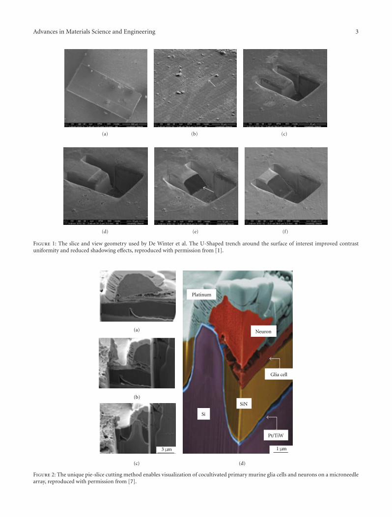
Advances in Materials Science and Engineering 3
(a) (b) (c)
(d) (e) (f)
Figure 1: The slice and view geometry used by De Winter et al. The U-Shaped trench around the surface of interest improved contrastuniformity and reduced shadowing effects, reproduced with permission from [1].
Platinum
Neuron
Si
SiN
Pt/TiW
1μm3μm
(a)
(b)
(c) (d)
Glia cell
Figure 2: The unique pie-slice cutting method enables visualization of cocultivated primary murine glia cells and neurons on a microneedlearray, reproduced with permission from [7].
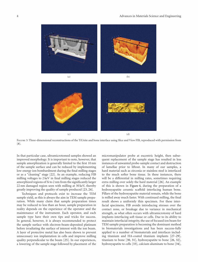
4 Advances in Materials Science and Engineering
(a) (b)
(c) (d)
Figure 3: Three-dimensional reconstructions of the TiUnite and bone interface using Slice and View FIB, reproduced with permission from[8].
In that particular case, ultramicrotomed samples showed animproved morphology. It is important to note, however, thatsample amorphization is generally limited to the first 10 nmof the sample surface and can be reduced by implementinglow-energy ion bombardment during the final milling stagesor as a “cleaning” stage [22]. As an example, reducing FIBmilling voltages to 2 keV in final milling stages reduced theamorphized regions of Si to 2 nm from the significantly larger22 nm damaged region seen with milling at 30 keV, therebygreatly improving the quality of sample produced [23, 24].
Techniques and protocols exist to increase the TEMsample yield, as this is always the aim in TEM sample prepa-ration. While many claim that sample preparation timesmay be reduced to less than an hour, sample preparation inreality depends on the experience of the operator and themaintenance of the instrument. Each operator, and eachsample type have their own tips and tricks for success.In general, however, it is always recommended to protectthe sample surface with electron-beam-deposited platinumbefore irradiating the surface of interest with the ion beam.A layer of protective metal has also been shown to preventunnecessary ion implantation in cells and improve millingquality perpendicular to the beam [25]. In our experiences,a lowering of the sample stage followed by placement of the
micromanipulator probe at eucentric height, then subse-quent replacement of the sample stage has resulted in lessinstances of unwanted probe-sample contact and destructionof lamellae prior to liftout. In many of our samples, ahard material such as zirconia or stainless steel is interfacedto the much softer bone tissue. In these instances, therewill be a differential in milling rates, sometimes requiringextra milling over solely the hard material [26]. An exampleof this is shown in Figure 4, during the preparation of ahydroxyapatite ceramic scaffold interfacing human bone.Pillars of the hydroxyapatite material remain, while the boneis milled away much faster. With continued milling, the finalresult shows a uniformly thin specimen. For these inter-facial specimens, FIB avoids introducing stresses over thecontact zone, or breakage due to variance in mechanicalstrength, as what often occurs with ultramicrotomy of hardimplants interfacing soft tissue or cells. Due to its ability tomaintain interfacial integrity, the use of focused ion beam forTEM sample preparation is becoming the dominant methodin biomaterials investigations and has been success-fullyapplied to a number of biomaterials and interfaces includ-ing titanium and HA-coated titanium implants [27–29],titanium to bone [30, 31], hydroxyapatite to bone [26, 32],hydroxyapatite to cells [33], calcium aluminate to bone [34],
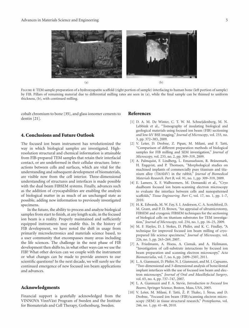
Advances in Materials Science and Engineering 5
4μm
(a)
2μm
(b)
Figure 4: TEM sample preparation of a hydroxyapatite scaffold (right portion of sample) interfacing to human bone (left portion of sample)by FIB. Pillars of remaining material due to differential milling rates are seen in (a), while the final sample can be thinned to uniformthickness, (b), with continued milling.
cobalt chromium to bone [35], and glass ionomer cements todentin [21].
4. Conclusions and Future Outlook
The focused ion beam instrument has revolutionized theway in which biological samples are investigated. High-resolution structural and chemical information is attainablefrom FIB-prepared TEM samples that retain their interfacialcontact, or are undeformed in their cellular structure. Inter-actions between cells and surfaces, which are vital for theunderstanding and subsequent development of biomaterials,are visible now from the cell interior. Three-dimensionalunderstanding of structures and interfaces is made possiblewith the dual beam FIBSEM systems. Finally, advances suchas the addition of cryocapabilities are enabling the analysisof biological matter in as much of an unchanged state aspossible, adding new information to previously investigatedspecimens.
In the future, the ability to process and analyze biologicalsamples from start to finish, at any length scale, in the focusedion beam is a reality. Properly maintained and sufficientlyequipped instruments may enable this. In the history ofFIB development, we have noted the shift in usage fromprimarily microelectronics and materials science based, toa user community that encompasses many areas includingthe life sciences. The challenge in the next phase of FIBdevelopment then shifts to, in what other ways can we use theFIB? What other devices can we couple with the instrumentor what changes can be made to provide answers to ourscientific questions? In the next decade, we will surely see thecontinued emergence of new focused ion beam applicationsand advances.
Acknowledgments
Financial support is gratefully acknowledged from theVINNOVA VinnVaxt Program of Sweden and the Institutefor Biomaterials and Cell Therapy, Gothenburg, Sweden.
References
[1] D. A. M. De Winter, C. T. W. M. Schneijdenberg, M. N.Lebbink et al., “Tomography of insulating biological andgeological materials using focused ion beam (FIB) sectioningand low-kV BSE imaging,” Journal of Microscopy, vol. 233, no.3, pp. 372–383, 2009.
[2] V. Leser, D. Drobne, Z. Pipan, M. Milani, and F. Tatti,“Comparison of different preparation methods of biologicalsamples for FIB milling and SEM investigation,” Journal ofMicroscopy, vol. 233, no. 2, pp. 309–319, 2009.
[3] A. Palmquist, F. Lindberg, L. Emanuelsson, R. Branemark,H. Engqvist, and P. Thomsen, “Morphological studies onmachined implants of commercially pure titanium and tita-nium alloy (Ti6Al4V) in the rabbit,” Journal of BiomedicalMaterials Research. Part B, vol. 91, no. 1, pp. 309–319, 2009.
[4] E. Lamers, X. F. Walboomers, M. Domanski et al., “Cryodualbeam focused ion beam-scanning electron microscopyto evaluate the interface between cells and nanopatternedscaffolds,” Tissue Engineering. Part C, vol. 17, no. 1, pp. 1–7,2010.
[5] H. K. Edwards, M. W. Fay, S. I. Anderson, C. A. Scotchford, D.M. Grant, and P. D. Brown, “An appraisal of ultramicrotomy,FIBSEM and cryogenic FIBSEM techniques for the sectioningof biological cells on titanium substrates for TEM investiga-tion,” Journal of Microscopy, vol. 234, no. 1, pp. 16–25, 2009.
[6] M. F. Hayles, D. J. Stokes, D. Phifer, and K. C. Findlay, “Atechnique for improved focused ion beam milling of cryo-prepared life science specimens,” Journal of Microscopy, vol.226, no. 3, pp. 263–269, 2007.
[7] A. Friedmann, A. Hoess, A. Cismak, and A. Heilmann,“Investigation of cell-substrate interactions by focused ionbeam preparation and scanning electron microscopy,” ActaBiomaterialia, vol. 7, no. 6, pp. 2499–2507, 2011.
[8] L. A. Giannuzzi, D. Phifer, N. J. Giannuzzi, and M. J. Capuano,“Two-dimensional and 3-dimensional analysis of bone/dentalimplant interfaces with the use of focused ion beam and elec-tron microscopy,” Journal of Oral and Maxillofacial Surgery,vol. 65, no. 4, pp. 737–747, 2007.
[9] L. A. Giannuzzi and F. A. Stevie, Introduction to Focused IonBeams, Springer Science, Boston, Mass, USA, 2005.
[10] V. Leser, M. Milani, F. Tatti, Z. P. Tkalec, J. Strus, and D.Drobne, “Focused ion beam (FIB)/scanning electron micro-scopy (SEM) in tissue structural research,” Protoplasma, vol.246, no. 1, pp. 41–48, 2010.
6 Advances in Materials Science and Engineering
[11] V. Raffa, O. Vittorio, V. Pensabene, A. Menciassi, and P.Dario, “FIB-nanostructured surfaces and investigation ofbio/nonbio interactions at the nanoscale,” IEEE Transactionson Nanobioscience, vol. 7, no. 1, pp. 1–10, 2008.
[12] E. Martınez, E. Engel, C. Lopez-Iglesias, C. A. Mills, J. A.Planell, and J. Samitier, “Focused ion beam/scanning electronmicroscopy characterization of cell behavior on polymermicro-/nanopatterned substrates: a study of cell-substrateinteractions,” Micron, vol. 39, no. 2, pp. 111–116, 2008.
[13] F. Schmidt, M. Kuhbacher, U. Gross, A. Kyriakopoulos, H.Schubert, and R. Zehbe, “From 2D slices to 3D volumes: imagebased reconstruction and morphological characterization ofhippocampal cells on charged and uncharged surfaces usingFIB/SEM serial sectioning,” Ultramicroscopy, vol. 111, no. 4,pp. 259–266, 2011.
[14] J. A. W. Heymann, M. Hayles, I. Gestmann, L. A. Giannuzzi, B.Lich, and S. Subramaniam, “Site-specific 3D imaging of cellsand tissues with a dual beam microscope,” Journal of StructuralBiology, vol. 155, no. 1, pp. 63–73, 2006.
[15] M. Marko, C. Hsieh, R. Schalek, J. Frank, and C. Mannella,“Focused-ion-beam thinning of frozen-hydrated biologicalspecimens for cryo-electron microscopy,” Nature Methods, vol.4, no. 3, pp. 215–217, 2007.
[16] M. W. Phaneuf, “Applications of focused ion beam microscopyto materials science specimens,” Micron, vol. 30, no. 3, pp.277–288, 1999.
[17] L. A. Giannuzzi and F. A. Stevie, “A review of focused ion beammilling techniques for TEM specimen preparation,” Micron,vol. 30, no. 3, pp. 197–204, 1999.
[18] J. Li, T. Malis, and S. Dionne, “Recent advances in FIB-TEMspecimen preparation techniques,” Materials Characterization,vol. 57, no. 1, pp. 64–70, 2006.
[19] D. M. Wright, J. J. Rickard, N. H. Kyle et al., “The use ofdual beam ESEM FIB to reveal the internal ultrastructure ofhydroxyapatite nanoparticle-sugar-glass composites,” Journalof Materials Science: Materials in Medicine, vol. 20, no. 1, pp.203–214, 2009.
[20] V. Jantou, M. Turmaine, G. D. West, M. A. Horton, and D. W.McComb, “Focused ion beam milling and ultramicrotomy ofmineralised ivory dentine for analytical transmission electronmicroscopy,” Micron, vol. 40, no. 4, pp. 495–501, 2009.
[21] E. Coutinho, T. Jarmar, F. Svahn et al., “Ultrastructuralcharacterization of tooth-biomaterial interfaces prepared withbroad and focused ion beams,” Dental Materials, vol. 25, no.11, pp. 1325–1337, 2009.
[22] N. I. Kato, “Reducing focused ion beam damage to trans-mission electron microscopy samples,” Journal of ElectronMicroscopy, vol. 53, no. 5, pp. 451–458, 2004.
[23] LA Giannuzzi, R Geurts, and J. Ringnalda, “2 keV Ga+FIB milling for reducing amorphous damage in silicon,”Microscopy and Microanalysis, vol. 11, no. S02, pp. 828–829,2005.
[24] L. A. Giannuzzi, “Reducing FIB damage using low energyions,” Microscopy and Microanalysis, vol. 12, no. 2, pp. 1260–1261, 2006.
[25] D. Drobne, M. Milani, V. Leser, and F. Tatti, “Surface damageinduced by FIB milling and imaging of biological samples iscontrollable,” Microscopy Research and Technique, vol. 70, no.10, pp. 895–903, 2007.
[26] K Grandfield, A Palmquist, F Ericson et al., “Bone responseto free-form fabricated hydroxyapatite and zirconia scaffolds:a transmission electron microscopy study in the humanmaxilla,” Clinical Implant Dentistry and Related Research, Feb11, 2010. In press.
[27] T. Jarmar, A. Palmquist, R. Branemark, L. Hermansson, H.Engqvist, and P. Thomsen, “Technique for preparation andcharacterization in cross-section of oral titanium implantsurfaces using focused ion beam and transmission electronmicroscopy,” Journal of Biomedical Materials Research. Part A,vol. 87, no. 4, pp. 1003–1009, 2008.
[28] M. Iliescu, V. Nelea, J. Werckmann, and I. N. Mihailescu,“Transmission electron microscopy investigation of pulsed-laser deposited hydroxylapatite thin films prepared by tripodand focused ion beam techniques,” Surface and CoatingsTechnology, vol. 187, no. 1, pp. 131–140, 2004.
[29] F. Lindberg, J. Heinrichs, F. Ericson, P. Thomsen, and H.Engqvist, “Hydroxylapatite growth on single-crystal rutilesubstrates,” Biomaterials, vol. 29, no. 23, pp. 3317–3323, 2008.
[30] A. Palmquist, F. Lindberg, L. Emanuelsson, R. Branemark, H.Engqvist, and P. Thomsen, “Biomechanical, histological, andultrastructural analyses of laser micro- and nano-structuredtitanium alloy implants: a study in rabbit,” Journal of Biomed-ical Materials Research. Part A, vol. 92, no. 4, pp. 1476–1486,2010.
[31] H. Engqvist, G. A. Botton, M. Couillard et al., “A novel toolfor high-resolution transmission electron microscopy of intactinterfaces between bone and metallic implants,” Journal ofBiomedical Materials Research. Part A, vol. 78, no. 1, pp. 20–24, 2006.
[32] K. Grandfield, E. A. McNally, A. Palmquist, G. A. Botton, P.Thomsen, and H. Engqvist, “Visualizing biointerfaces in threedimensions: electron tomography of the bone-hydroxyapatiteinterface,” Journal of the Royal Society Interface, vol. 7, no. 51,pp. 1497–1501, 2010.
[33] H. Engqvist, F. Svahn, T. Jarmar et al., “A novel method forproducing electron transparent films of interfaces betweencells and biomaterials,” Journal of Materials Science: Materialsin Medicine, vol. 19, no. 1, pp. 467–470, 2008.
[34] A. Palmquist, T. Jarmar, L. Hermansson et al., “Calciumaluminate coated and uncoated free form fabricated cocrimplants: a comparative study in rabbit,” Journal of BiomedicalMaterials Research. Part B, vol. 91, no. 1, pp. 122–127, 2009.
[35] K. Grandfield, A. Palmquist, S. Goncalves et al., “Free formfabricated features on CoCr implants with and withouthydroxyapatite coating in vivo: a comparative study of bonecontact and bone growth induction,” Journal of MaterialsScience: Materials in Medicine, vol. 22, no. 4, pp. 899–906,2011.

Hindawi Publishing CorporationAdvances in Materials Science and EngineeringVolume 2012, Article ID 640217, 6 pagesdoi:10.1155/2012/640217
Research Article
Application of Resonant Nuclear Reactions forStudying the Diffusion of Nitrogen and Silicon inTi-Modified Stainless Steel
J. Arunkumar, C. David, K. G. M. Nair, B. K. Panigrahi, and C. S. Sundar
Materials Science Group, Indira Gandhi Centre for Atomic Research, Kalpakkam 603 102, India
Correspondence should be addressed to K. G. M. Nair, [email protected]
Received 1 April 2011; Revised 13 June 2011; Accepted 17 June 2011
Academic Editor: Adam Georg Balogh
Copyright © 2012 J. Arunkumar et al. This is an open access article distributed under the Creative Commons Attribution License,which permits unrestricted use, distribution, and reproduction in any medium, provided the original work is properly cited.
Resonant nuclear reaction analysis can be used for the study of diffusion behaviour of minor alloying elements in reactor structuralmaterials. In the present paper, 15N(p,αγ)12C and 30Si(p,γ)31P reactions have been used to profile the ion-implanted 15N and 30Siin D9 alloy (titanium-modified austenitic stainless steel). The diffusion coefficients at various temperatures have been estimatedfrom the broadening of the implantation profiles during thermal annealing, and the activation energies are deduced.
1. Introduction
The structural materials like fuel clad and wrapper insodium-cooled fast reactors are exposed to a hostile envi-ronment of intense fast neutron bombardment at elevatedtemperatures. One of the main problems which result onaccount of the radiation damage is the dimensional changesbrought about by void swelling, leading to a decreasedresidence time of the fuel assemblies in the reactor coreand lowering of fuel burnup. Therefore, resistance to voidswelling is a major consideration in the choice of materialsfor the core components.
Improvement in the resistance to irradiation-inducedvoid swelling can be achieved by the introduction of efficienttraps for vacancies and helium such as dislocations andprecipitate-matrix interfaces, by adjusting alloying elementsand through thermomechanical treatments [1, 2]. Thetitanium-modified steel exhibits improved swelling resis-tance under breeder reactor conditions and, consequently,has become a prime candidate for structural applications[3]. The role of fast diffusing alloying elements, namely, Ti,Si, and P in suppressing void nucleation is known [4]. Thefast diffusing species increases the effective vacancy diffusioncoefficient, and the consequent reduction in the void nucle-ation rates plays a crucial role in imparting significant void
swelling resistance to the alloy. In order to model such effects,knowledge of the diffusion behavior of constituent speciesis essential due to their considerable redistribution duringirradiation. Therefore, thermal diffusion behavior of soluteslike silicon and nitrogen in titanium-modified steels has beenstudied here.
Though some amount of studies on the effect of minoralloying elements on the self-diffusion of the constituentelements have been carried out [5], reports on the diffusionbehavior of silicon in SS 316 are sparse, and to the best ofour knowledge, there is hardly any literature describing thediffusion behavior of silicon in titanium-modified steels.
Also, studies concerning iron-based alloys and theirvariants with interstitial solute additions (C, N) continueto attract attention due to the rich technological interest inimproving radiation resistance, mechanical and tribologicalproperties. In nitriding processes involving ion implantation,an improvement in mechanical property is achieved due tothe increased quantity of interstitial nitrogen and their inter-action with crystal defects. There also exists an alternativeconjecture that the trapping of vacancies with interstitialimpurity atoms enhances the probability of recombination,hence aiding in reduction of void swelling. Thus, practicalapplications have necessitated a full understanding of theunderlying physical processes involving interstitial solutes,
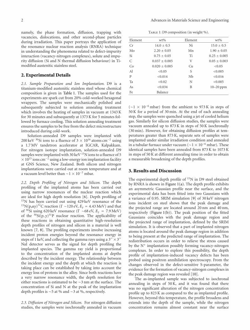
2 Advances in Materials Science and Engineering
namely, the phase formation, diffusion, trapping withvacancies, dislocations, and other second-phase particlesduring irradiation. This paper portrays the application ofthe resonance nuclear reaction analysis (RNRA) techniquein understanding the phenomena related to defect-impurityinteraction (vacancy-nitrogen complexes), solute and impu-rity diffusion (Si and N thermal diffusion behaviour) in Ti-modified austenitic stainless steel.
2. Experimental Details
2.1. Sample Preparation and Ion Implantation. D9 is atitanium-modified austenitic stainless steel whose chemicalcomposition is given in Table 1. The samples used for theexperiments are spark cut from 20% cold-worked hexagonalwrappers. The samples were mechanically polished andsubsequently subjected to solution annealing treatmentwhich involves the heating of samples in vacuum at 1343 Kfor 30 minutes and subsequently at 1373 K for 5 minutes fol-lowed by furnace cooling. This solution annealing treatmentensures the samples to be free from the defect microstructureintroduced during cold-work.
Solution-annealed D9 samples were implanted with200 keV 30Si ions to a fluence of 3 × 10¹⁶ atoms cm−2 usinga 1.7 MV tandetron accelerator at IGCAR, Kalpakkam.For nitrogen isotope implantation, solution-annealed D9samples were implanted with 30 keV 15N ions to a fluence of 5× 10¹⁵ ions cm−2 using a low-energy ion implantation facilityat GNS Science, New Zealand. Both silicon and nitrogenimplantations were carried out at room temperature and ata vacuum level better than ∼1 × 10⁻⁷ mbar.
2.2. Depth Profiling of Nitrogen and Silicon. The depthprofiling of the implanted atoms has been carried outusing narrow resonances of the nuclear reaction whichare ideal for high depth resolution [6]. Depth profiling of15N has been carried out using 429 keV resonance of the15N(p,αγ)12C reaction (Γ ∼120 eV, Eγ = 4.43 MeV) and thatof 30Si using 620 keV resonance (Γ ∼68 eV, Eγ = 7.9 MeV)of the 30Si(p, γ)31P nuclear reaction. The applicability ofthese reactions in obtaining quantitative high-resolutiondepth profiles of nitrogen and silicon in a material is wellknown [7, 8]. The profiling experiments involve increasingincident proton energies beyond the resonance energy insteps of 1 keV, and collecting the gamma rays using a 3′′ ×3′′
NaI detector serves as the signal for depth profiling theimplanted species. The gamma ray yield is proportionalto the concentration of the implanted atoms at depthsdescribed by the incident energy. The relationship betweenthe incident energy and the depth at which the reaction istaking place can be established by taking into account theenergy loss of protons in the alloy. Since both reactions havea very narrow resonance width, the depth resolution foreither reactions is estimated to be ∼3 nm at the surface. Theconcentration of Si and N at the peak of the implantationdepth profiles is ∼5 at % and ∼3 at %, respectively.
2.3. Diffusion of Nitrogen and Silicon. For nitrogen diffusionstudies, the samples were isochronally annealed in vacuum
Table 1: D9 composition (in weight %).
Element wt% Element wt%
Cr 14.0 ± 0.5 Ni 15.0 ± 0.5
Mo 2.20 ± 0.05 Mn 1.90 ± 0.05
Si 0.75 ± 0.05 Ti 0.25 ± 0.005
C 0.037 ± 0.005 V 0.05 ± 0.003
Co 0.020 ± 0.005 Cu <0.05
Al <0.05 S <0.005
P <0.014 Nb <0.016
Ta <0.02 N <0.005
As <0.034 B 10–20 ppm
Fe Balance
(∼1 × 10⁻⁶ mbar) from the ambient to 973 K in steps of50 K for a period of 30 min. At the end of each annealingstep, the samples were quenched using a jet of cooled heliumgas. Similarly for silicon diffusion studies, the samples werevacuum annealed up to 873 K in steps of 50 K isochronally(30 min). However, for obtaining diffusion profiles at tem-peratures greater than 873 K, separate sets of samples wereimplanted under similar irradiation condition and annealedin a tubular furnace under vacuum (∼1× 10⁻⁶ mbar). Theseidentical samples have been annealed from 873 K to 1073 Kin steps of 50 K at different annealing time in order to obtaina measurable broadening of the depth profiles.
3. Results and Discussion
The experimental depth profile of 15N in D9 steel obtainedby RNRA is shown in Figure 1(a). The depth profile exhibitsan asymmetric Gaussian profile near the surface, and theexperimental data has been fitted into two Gaussians witha variance of 0.95. SRIM simulation [9] of 30 keV nitrogenions incident on steel shows that the peak damage andthe projected range are located around 20 nm and 40 nm,respectively (Figure 1(b)). The peak position of the fittedGaussians coincides with the peak damage region andthe projected range of implantation, defined by the SRIMsimulation. It is observed that a part of implanted nitrogenatoms is located around the peak damage region in additionto being present at the predicted range of implantation. Theredistribution occurs in order to relieve the stress causedby the N+ implantation possibly forming vacancy-nitrogencomplexes. In order to explore this possibility, the depthprofile of implantation-induced vacancy defects has beenprobed using positron annihilation spectroscopy. From thechanges observed in the defect-sensitive S-parameter, theevidence for the formation of vacancy-nitrogen complexes inthe peak damage region was revealed [10].
The as-implanted sample was subjected to isochronalannealing in steps of 50 K, and it was found that therewas no significant alteration of the nitrogen concentrationprofile up to 823 K as compared to the as implanted profile.However, beyond this temperature, the profile broadens andextends into the depth of the sample, while the nitrogenconcentration remains almost constant near the surface
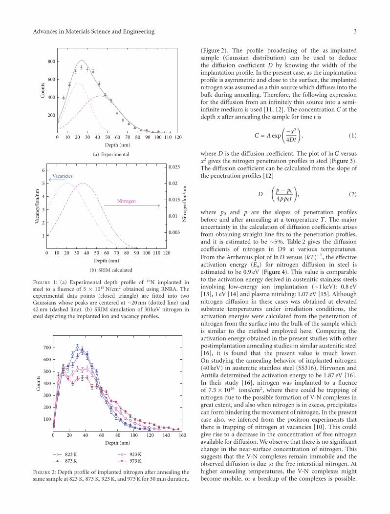
Advances in Materials Science and Engineering 3
0 10 20 30 40 50 60 70 80 90 100 110
200
400
600
800
Cou
nts
Depth (nm)
120
(a) Experimental
Vac
ancy
/Ion
/nm
0.005
0.01
0.015
0.02
0.025
Nit
roge
n/I
on/n
m
Vacancies
Nitrogen
1
2
3
4
5
6
0 10 20 30 40 50 60 70 80 90 100 110
Depth (nm)
120
(b) SRIM calculated
Figure 1: (a) Experimental depth profile of 15N implanted insteel to a fluence of 5 × 10¹⁵ N/cm2 obtained using RNRA. Theexperimental data points (closed triangle) are fitted into twoGaussians whose peaks are centered at ∼20 nm (dotted line) and42 nm (dashed line). (b) SRIM simulation of 30 keV nitrogen insteel depicting the implanted ion and vacancy profiles.
0 20 40 60 80 100 120 140 160
100
200
300
400
500
600
700
823 K873 K
923 K973 K
Cou
nts
Depth (nm)
Figure 2: Depth profile of implanted nitrogen after annealing thesame sample at 823 K, 873 K, 923 K, and 973 K for 30 min duration.
(Figure 2). The profile broadening of the as-implantedsample (Gaussian distribution) can be used to deducethe diffusion coefficient D by knowing the width of theimplantation profile. In the present case, as the implantationprofile is asymmetric and close to the surface, the implantednitrogen was assumed as a thin source which diffuses into thebulk during annealing. Therefore, the following expressionfor the diffusion from an infinitely thin source into a semi-infinite medium is used [11, 12]. The concentration C at thedepth x after annealing the sample for time t is
C = A exp
(−x2
4Dt
), (1)
where D is the diffusion coefficient. The plot of lnC versusx2 gives the nitrogen penetration profiles in steel (Figure 3).The diffusion coefficient can be calculated from the slope ofthe penetration profiles [12]
D =(p − p0
4pp0t
), (2)
where p0 and p are the slopes of penetration profilesbefore and after annealing at a temperature T . The majoruncertainty in the calculation of diffusion coefficients arisesfrom obtaining straight line fits to the penetration profiles,and it is estimated to be ∼5%. Table 2 gives the diffusioncoefficients of nitrogen in D9 at various temperatures.From the Arrhenius plot of lnD versus (kT)−1, the effectiveactivation energy (Ea) for nitrogen diffusion in steel isestimated to be 0.9 eV (Figure 4). This value is comparableto the activation energy derived in austenitic stainless steelsinvolving low-energy ion implantation (∼1 keV): 0.8 eV[13], 1 eV [14] and plasma nitriding: 1.07 eV [15]. Althoughnitrogen diffusion in these cases was obtained at elevatedsubstrate temperatures under irradiation conditions, theactivation energies were calculated from the penetration ofnitrogen from the surface into the bulk of the sample whichis similar to the method employed here. Comparing theactivation energy obtained in the present studies with otherpostimplantation annealing studies in similar austenitic steel[16], it is found that the present value is much lower.On studying the annealing behavior of implanted nitrogen(40 keV) in austenitic stainless steel (SS316), Hirvonen andAnttila determined the activation energy to be 1.87 eV [16].In their study [16], nitrogen was implanted to a fluenceof 7.5 × 10¹⁶ ions/cm2, where there could be trapping ofnitrogen due to the possible formation of V-N complexes ingreat extent, and also when nitrogen is in excess, precipitatescan form hindering the movement of nitrogen. In the presentcase also, we inferred from the positron experiments thatthere is trapping of nitrogen at vacancies [10]. This couldgive rise to a decrease in the concentration of free nitrogenavailable for diffusion. We observe that there is no significantchange in the near-surface concentration of nitrogen. Thissuggests that the V-N complexes remain immobile and theobserved diffusion is due to the free interstitial nitrogen. Athigher annealing temperatures, the V-N complexes mightbecome mobile, or a breakup of the complexes is possible.

4 Advances in Materials Science and Engineering
0 2000 4000 6000 8000 10000 12000 140007
20
55
148
403
1097
923 K873 K823 K 973 K
Cou
nts
Sq. depth (nm2)
Figure 3: Penetration profiles (lnC versus x2) derived fromdepth profiles of nitrogen obtained after annealing at differenttemperatures in D9 steel.
Table 2: Diffusion coefficients of N in D9.
Temperature (K) Time (103 sec) Diffusion coefficient (m2/sec)
873 1.8 6.1 × 10⁻¹⁶
923 1.8 1.2 × 10⁻¹⁵
973 1.8 2.1 × 10⁻¹⁵
Table 3: Diffusion coefficients of Si in D9.
Temperature (K) Time (103 sec) Diffusion coefficient D (m2/sec)
873 39.6 4.6 × 10⁻²⁰
923 18 1.3 × 10⁻¹⁹
973 3.6 8.8 × 10⁻¹⁹
1023 3.6 2.6 × 10⁻¹⁸
1073 0.9 6.5 × 10⁻¹⁸
In fact, small changes in the near surface composition ofnitrogen is observed as a function of annealing temperature,and a more detailed study of this might throw light on theevolution of the nitrogen trapped at vacancies.
Proceeding to the next study in 30Si-implanted D9samples, the experimentally obtained depth distribution ofthe as-implanted silicon is illustrated in Figure 5, whichis a Gaussian profile with centre and full width at half-maximum (FWHM) as 120 nm and 95 nm, respectively.The experimentally determined depth profile is in goodagreement with the theoretical profile computed from SRIMprogram [9]. It should be noted here that there is noredistribution of implanted silicon quite contrary to theobservation in nitrogen implantation. The absence of sucha redistribution of the implanted silicon may be due to thepresence of silicon in substitutional position of the hostlattice. This implanted silicon distribution serves as themarker layer, and its broadening is used for following thediffusion behavior of silicon in D9 samples.
The silicon implanted sample was annealed in steps of50 K in vacuum for a period of 30 min at each step followedby RNRA experiments after each annealing. It is found that
12 12.5 13 13.5
5E− 16
6E− 16
7E− 168E− 169E− 161E− 15
2E− 15
3E− 15
D(m
2/s
)
N di usion
1/kT (eV− 1)
Figure 4: Arrhenius plot to estimate activation energy for nitrogendiffusion in D9 steel.
there is no significant change in the width of the implantedprofile in the sample up to 873 K with the annealing timeof half an hour. After prolonged annealing at 873 K for fewhours followed by RNRA experiment at different incrementsof time, the implantation profile showed a discernible changeafter eleven hours (Figure 5). Further, four numbers of Si-implanted D9 samples were annealed independently at fourdifferent temperatures from 923 K to 1073 K in steps of 50 Kfor different durations. Figure 5 shows the diffusion profileof silicon in the temperature interval of 873 K to 1073 K,and the annealing time for each temperature is indicatedin the figure. At higher annealing temperatures beyond973 K, segregation of Si towards the surface is also observed.However, broadening of depth profiles in this temperatureregime is quite evident. The method used for estimatingN diffusion coefficients is employed for Si diffusion also.Figure 6 shows the penetration profiles of Si in D9 atvarious temperatures with the respective annealing time. Theaccuracy of the calculated D values is limited by the linearfitting of the slopes (error less than ∼10%). The diffusioncoefficients at different annealing temperatures are tabulatedin Table 3. From the Arrhenius plot of lnD versus the inverseof kT (Figure 7), activation energy of 2.1 eV is obtained forthe silicon diffusion in D9 steel.
The activation energy for silicon diffusion in the presentexperiment may be compared to the self-diffusion energy ofiron (2.84 eV) in fcc-Fe [17], and it is also comparable withthe diffusion of alloying elements like nickel (2.72 eV), iron(2.60 eV), and chromium (2.51 eV) reported in austeniticstainless steel [5]. In addition, the activation energy deducedhere for silicon diffusion is much greater than the exper-imentally determined effective vacancy migration energy(1.13 eV) in solution-annealed D9 steel [18]. Hence, silicondiffusion in the solution annealed D9 steel is regardedto be a vacancy-assisted mechanism. The present valueof activation energy for silicon diffusion is lower than apreviously reported value of 2.43 eV for silicon diffusion infcc-Fe [17]. Addition of fast diffusing solutes can increase thevacancy migration and in turn the diffusion of solvent atoms.Evidences exist in the literature with respect to the increase

Advances in Materials Science and Engineering 5
0
50
100
150
200
250
300
350
0 50 100 150 200 250 300
As-implanted873 K/660 min
923 K/300 min973 K/60 min
Cou
nts
Depth (nm)
(a)
As-implanted1073 K/15 min1023 K/60 min
0
50
100
150
200
250
300
350
0 50 100 150 200 250 300
Cou
nts
Depth (nm)
(b)
Figure 5: The broadening of the depth profile of implanted 30Si determined by RNRA measurements at different annealing temperatures.
0 20000 40000 60000 80000
20
55
148
403
As-implanted873 K/660 min923 K/300 min
973 K/60 min1023 K/60 min1073 K/15 min
Cou
nts
Sq. depth (nm2)
Figure 6: Penetration profiles of the silicon obtained after annealingthe independently implanted samples at different temperatures inD9 steel.
in the diffusivity of major alloying elements like Fe, Cr, andNi due to silicon additions [5, 19]. It should be noted thatanother fast diffusing species, namely titanium is present inD9 steel. Titanium being an oversized element in the D9alloy would diffuse via vacancy mechanism. In a work byOkita et al. [20] to understand the effect of titanium onvoid swelling, studies were carried out on solution-annealedaustenitic Fe-15Cr-16Ni ternary alloys (similar wt% of Crand Ni in D9 steel) without titanium and with the additionof 0.25 wt% of Ti (similar wt% of Ti in D9 steel). In thatpaper [20], reduction in void nucleation due to titanium
10.5 11 11.5 12 12.5 13 13.5
1E− 19
1E− 18
1E− 17Si di usion
D(m
2/s
)
1/kT (eV− 1)
Figure 7: Arrhenius plot for the determination of activation energyfor Si diffusion in D9 steel.
addition was attributed to the enhancement of the effectivevacancy diffusion coefficient. Hence, the reason for therelatively lower activation energy obtained here for silicondiffusion in solution-annealed D9 steel is ascribed to theincreased vacancy migration due to the presence of bothsilicon and titanium in D9 steels. Therefore, the presentobservation strongly suggests that the synergetic effects dueto the presence of various fast diffusing solutes contribute toenhanced vacancy mobility and the consequent void swellingsuppression.
4. Conclusions
Resonant nuclear reaction analysis has been utilized to obtainthe diffusion profiles of nitrogen and silicon in Ti-modifiedstainless steel. Results show that in the temperature rangeof annealing, a fraction of nitrogen remains trapped near

6 Advances in Materials Science and Engineering
the surface possibly vacancy-nitrogen complexes, and theactivation energy for diffusion of free nitrogen is obtained.The thermal diffusion behavior of silicon in titanium-modified steel is also determined. From the estimatedactivation energy, it can be concluded that in a thermalenvironment silicon diffuses by vacancy mechanism in steel.
Acknowledgment
The authors gratefully acknowledge Dr. John Kennedy,Senior Scientist, National Isotope Centre, GNS Science, NewZealand for nitrogen implantation.
References
[1] L. K. Mansur, E. H. Lee, P. J. Maziasz, and A. P. Rowcliffe,“Control of helium effects in irradiated materials based ontheory and experiment,” Journal of Nuclear Materials, vol. 141–143, no. 2, pp. 633–646, 1986.
[2] W. Kesternich, “A possible solution of the problem of heliumembrittlement,” Journal of Nuclear Materials, vol. 127, no. 2-3,pp. 153–160, 1985.
[3] A. F. Rowcliffe and M. L. Grossbeck, “The response ofaustenitic steels to radiation damage,” Journal of NuclearMaterials, vol. 122-123, no. 1–3, pp. 181–190, 1984.
[4] P. J. Maziasz, “Void swelling resistance of phosphorus-modified austenitic stainless steels during HFIR irradiation at300–500◦C to 57 dpa,” Journal of Nuclear Materials, vol. 200,no. 1, pp. 90–107, 1993.
[5] W. Assassa and P. Guiraldenq, “Bulk and grain boundarydiffusion of 59Fe, 51Cr and 63Ni in austenitic stainless steelunder the influence of silicon content,” Metal Science, vol. 12,no. 3, pp. 123–128, 1978.
[6] B. Maurel, G. Amsel, and J. P. Nadai, “Depth profilingwith narrow resonances of nuclear reactions: theory andexperimental use,” Nuclear Instruments and Methods In PhysicsResearch, vol. 197, no. 1, pp. 1–13, 1982.
[7] S. Kumar, S. V. Kumar, G. L. N. Reddy, V. Kain, J. V. Ramana,and V. S. Raju, “Depth profiling of nitrogen using 429 keV and897 keV resonances in the 15N(p,αγ)12C reaction,” NuclearInstruments and Methods in Physics Research, Section B, vol.240, no. 3, pp. 704–710, 2005.
[8] D. J. Cherniak, “Silicon self-diffusion in single-crystal naturalquartz and feldspar,” Earth and Planetary Science Letters, vol.214, no. 3-4, pp. 655–668, 2003.
[9] J. F. Ziegler, J. P. Biersack, and U. Littmark, The Stopping andRange of Ions in Solids, Pergamon, New York, NY, USA, 1985.
[10] J. Arunkumar, C. David, C. Varghese Anto et al., “A study onthe redistribution of ion-implanted nitrogen in Ti-modifiedaustenitic steel,” Journal of Nuclear Materials, vol. 414, no. 3,pp. 382–385, 2011.
[11] J. Crank, Mathematics of Diffusion, Clarendon, Oxford, UK,1975.
[12] F. L. Bregolin, M. Behar, and F. Dyment, “Diffusion studyof nitrogen implanted into α-Hf using the nuclear resonancetechnique,” Applied Physics A, vol. 95, no. 2, pp. 501–505, 2009.
[13] D. L. Williamson, J. A. Davis, P. J. Wilbur, J. J. Vajo, R. Wei,and J. N. Matossian, “Relative roles of ion energy, ion flux, andsample temperature in low-energy nitrogen ion implantationof Fe-Cr-Ni stainless steel,” Nuclear Instruments and Methodsin Physics Research, Section B, vol. 127-128, pp. 930–934, 1997.
[14] N. Tsubouchi, Y. Mokuno, A. Chayahara, and Y. Horino,“Nitrogen diffusion in stainless steel during irradiation withmass-selected low-energy N+ ion beams,” Surface and CoatingsTechnology, vol. 196, no. 1–3, pp. 271–274, 2005.
[15] E. Menthe and K. T. Rie, “Further investigation of thestructure and properties of austenitic stainless steel afterplasma nitriding,” Surface and Coatings Technology, vol. 116–119, pp. 199–204, 1999.
[16] J. Hirvonen and A. Anttila, “Annealing behavior of implantednitrogen in AISI 316 stainless steel,” Applied Physics Letters, vol.46, no. 9, pp. 835–836, 1985.
[17] D. Bergner, Y. Khaddour, and S. Lorx, “Diffusion of Si in bcc-and fcc-Fe,” Defect and Diffusion Forum, vol. 66–69, pp. 1407–1412, 1990.
[18] J. Arunkumar, S. Abhaya, R. Rajaraman et al., “Defect recoveryin proton irradiated Ti-modified stainless steel probed bypositron annihilation,” Journal of Nuclear Materials, vol. 384,no. 3, pp. 245–248, 2009.
[19] S. J. Rothman, L. J. Nowicki, and G. E. Murch, “Self-diffusionin austenitic Fe-Cr-Ni alloys,” Journal of Physics F: MetalPhysics, vol. 10, no. 3, article 009, pp. 383–398, 1980.
[20] T. Okita, W. G. Wolfer, F. A. Garner, and N. Sekimura, “Eff-ects of titanium additions to austenitic ternary alloys onmicrostructural evolution and void swelling,” PhilosophicalMagazine, vol. 85, no. 18, pp. 2033–2048, 2005.
Hindawi Publishing CorporationAdvances in Materials Science and EngineeringVolume 2012, Article ID 905474, 13 pagesdoi:10.1155/2012/905474
Review Article
Radiation Effects in Nuclear Ceramics
L. Thome,1 S. Moll,1 A. Debelle,1 F. Garrido,1 G. Sattonnay,2 and J. Jagielski3, 4
1 Centre de Spectrometrie Nucleaire et de Spectrometrie de Masse, CNRS/IN2P3 et Universite Paris-Sud, Bat. 108, 91405 Orsay, France2 LEMHE/ICMMO, UMR 8182, Universite Paris-Sud, Bat. 410, 91405 Orsay, France3 Institute for Electronic Materials Technology, Wolczynska 133, 01-919 Warsaw, Poland4 The Andrzej Soltan Institute for Nuclear Studies, 05-400 Swierk/Otwock, Poland
Correspondence should be addressed to L. Thome, [email protected]
Received 29 March 2011; Accepted 17 May 2011
Academic Editor: Robert G. Elliman
Copyright © 2012 L. Thome et al. This is an open access article distributed under the Creative Commons Attribution License,which permits unrestricted use, distribution, and reproduction in any medium, provided the original work is properly cited.
Due to outstanding physicochemical properties, ceramics are key engineering materials in many industrial domains. Theevaluation of the damage created in ceramics employed in radiative media is a challenging problem for electronic, space, andnuclear industries. In this latter field, ceramics can be used as immobilization forms for radioactive wastes, inert fuel matricesfor actinide transmutation, cladding materials for gas-cooled fission reactors, and structural components for fusion reactors.Information on the radiation stability of nuclear materials may be obtained by simulating the different types of interactionsinvolved during the slowing down of energetic particles with ion beams delivered by various types of accelerators. This paperpresents a review of the radiation effects occurring in nuclear ceramics, with an emphasis on recent results concerning the damageaccumulation processes. Energetic ions in the KeV-GeV range are used to explore the nuclear collision (at low energy) andelectronic excitation (at high energy) regimes. The recovery by electronic excitation of the damage created by ballistic collisions(SHIBIEC process) is also addressed.
1. Introduction
Ceramics are key engineering materials in many domains ofhuman activity due to outstanding physicochemical proper-ties, such as high strength, low-thermal expansion, chemicalstability, and good behavior under irradiation. Therefore,these materials are often employed in hostile media whereefficient use of energy is a prime need, for example, extremetemperatures, corrosive surroundings, and radiative envi-ronment. Industrial applications concern electronic, space,and nuclear fields. For instance, ceramics are nowadayswidely used for surface coating and electronic packaging,and they are envisioned in a near future as immobilizationforms for radioactive wastes, inert fuel matrices for actinidetransmutation, cladding materials for gas-cooled fissionreactors, and structural components for fusion reactors. Inmost of these applications, there is an urgent need of data fora fundamental understanding of the processes of radiationdamage.
Information on the radiation stability of nuclear mate-rials may be gained by simulating the different types of
interactions (nuclear and electronic) involved during theslowing down of energetic particles with ion beams deliv-ered by various types of low-, medium-, and high-energyaccelerators. A rather broad panoply of advanced techniques(e.g., Rutherford backscattering spectrometry in channelingconditions (RBS/C), X-ray diffraction (XRD), transmissionelectron microscopy (TEM), and Raman spectroscopy),which sense the investigated materials at various spatial scalesand with different sensitivities, can be implemented to (i)monitor the damage buildup, (ii) quantify the strain/stresslevel as a function of ion fluence, (iii) characterize radiationdefects, (iv) determine the formation of new phases, (v)specify the parameters which trigger the (micro)structuralchanges, and (vi) understand the mechanisms involved in thedamage formation. Results may then feed databases, be com-pared to computational works (using for instance moleculardynamics tools), and finally help the development of theo-retical models or at least of phenomenological descriptions.
The topic that is concerned here is extremely broad.A huge number of papers were published in the last threedecades on the damage production in nuclear materials, and
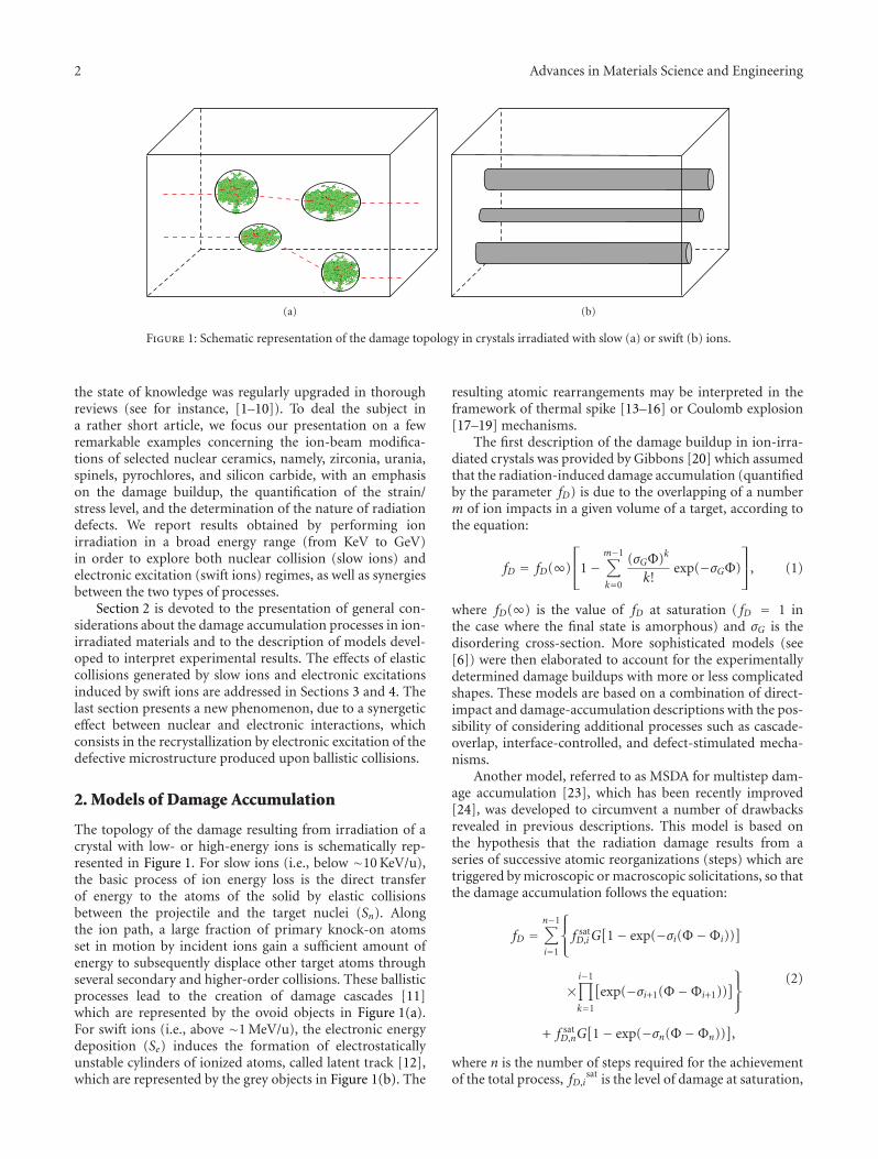
2 Advances in Materials Science and Engineering
(a) (b)
Figure 1: Schematic representation of the damage topology in crystals irradiated with slow (a) or swift (b) ions.
the state of knowledge was regularly upgraded in thoroughreviews (see for instance, [1–10]). To deal the subject ina rather short article, we focus our presentation on a fewremarkable examples concerning the ion-beam modifica-tions of selected nuclear ceramics, namely, zirconia, urania,spinels, pyrochlores, and silicon carbide, with an emphasison the damage buildup, the quantification of the strain/stress level, and the determination of the nature of radiationdefects. We report results obtained by performing ionirradiation in a broad energy range (from KeV to GeV)in order to explore both nuclear collision (slow ions) andelectronic excitation (swift ions) regimes, as well as synergiesbetween the two types of processes.
Section 2 is devoted to the presentation of general con-siderations about the damage accumulation processes in ion-irradiated materials and to the description of models devel-oped to interpret experimental results. The effects of elasticcollisions generated by slow ions and electronic excitationsinduced by swift ions are addressed in Sections 3 and 4. Thelast section presents a new phenomenon, due to a synergeticeffect between nuclear and electronic interactions, whichconsists in the recrystallization by electronic excitation of thedefective microstructure produced upon ballistic collisions.
2. Models of Damage Accumulation
The topology of the damage resulting from irradiation of acrystal with low- or high-energy ions is schematically rep-resented in Figure 1. For slow ions (i.e., below ∼10 KeV/u),the basic process of ion energy loss is the direct transferof energy to the atoms of the solid by elastic collisionsbetween the projectile and the target nuclei (Sn). Alongthe ion path, a large fraction of primary knock-on atomsset in motion by incident ions gain a sufficient amount ofenergy to subsequently displace other target atoms throughseveral secondary and higher-order collisions. These ballisticprocesses lead to the creation of damage cascades [11]which are represented by the ovoid objects in Figure 1(a).For swift ions (i.e., above ∼1 MeV/u), the electronic energydeposition (Se) induces the formation of electrostaticallyunstable cylinders of ionized atoms, called latent track [12],which are represented by the grey objects in Figure 1(b). The
resulting atomic rearrangements may be interpreted in theframework of thermal spike [13–16] or Coulomb explosion[17–19] mechanisms.
The first description of the damage buildup in ion-irra-diated crystals was provided by Gibbons [20] which assumedthat the radiation-induced damage accumulation (quantifiedby the parameter fD) is due to the overlapping of a numberm of ion impacts in a given volume of a target, according tothe equation:
fD = fD(∞)
⎡⎣1−
m−1∑k=0
(σGΦ)k
k!exp(−σGΦ)
⎤⎦, (1)
where fD(∞) is the value of fD at saturation ( fD = 1 inthe case where the final state is amorphous) and σG is thedisordering cross-section. More sophisticated models (see[6]) were then elaborated to account for the experimentallydetermined damage buildups with more or less complicatedshapes. These models are based on a combination of direct-impact and damage-accumulation descriptions with the pos-sibility of considering additional processes such as cascade-overlap, interface-controlled, and defect-stimulated mecha-nisms.
Another model, referred to as MSDA for multistep dam-age accumulation [23], which has been recently improved[24], was developed to circumvent a number of drawbacksrevealed in previous descriptions. This model is based onthe hypothesis that the radiation damage results from aseries of successive atomic reorganizations (steps) which aretriggered by microscopic or macroscopic solicitations, so thatthe damage accumulation follows the equation:
fD =n−1∑i=1
⎧⎨⎩ f sat
D,i G[1− exp(−σi(Φ−Φi))
]
×i−1∏k=1
[exp(−σi+1(Φ−Φi+1))
]⎫⎬⎭+ f sat
D,nG[1− exp(−σn(Φ−Φn))
],
(2)
where n is the number of steps required for the achievementof the total process, fD,i
sat is the level of damage at saturation,

Advances in Materials Science and Engineering 3
0
10
20
30
40
50
1000 1500 2000 2500
Energy (keV)
Yie
ld
O
Zr
Virgin
1015
1.5 × 10¹⁵
5 × 10¹⁵
2 × 10¹⁶
Random
<100> axis
(a)
0
0.1
0.2
0.3
0.4
0.5
0.6
0 500 1000 1500
Depth (nm)
Acc
um
ula
ted
dam
age
(fD
)
1015
1.5 × 10¹⁵
2 × 10¹⁵
5 × 10¹⁵
2 × 10¹⁶
(b)
Figure 2: (a) RBS spectra recorded on cubic zirconia crystals irradiated at RT with 4-MeV Au ions in random (stars) and 〈100〉-aligned(other symbols) directions (ion fluences are given in cm−2). Energy of analyzing He beam: 3.07 MeV. Solid lines are fits to experimental datawith the McChasy code [21, 22]. (b) Accumulated damage ( fD) as a function of depth extracted from the fits to experimental RBS data forcubic zirconia crystals irradiated with 4-MeV Au ions at the indicated fluences.
σi is the cross-section for damage formation, and Φi is thethreshold irradiation fluence, for the ith step. G is a functionwhich transforms negative values into 0 and leaves positivevalues unchanged.
Implementation of this model to the analysis of damagebuildups obtained for ion-irradiated test-case ceramics isprovided in the following two sections.
3. Effects of Elastic Collisions (Slow Ions)
Defect cascades created by low-energy ion irradiation areresponsible for a large variety of (micro)structural modi-fications (topological or chemical disorder, swelling, phasetransformations, polygonization, amorphization, etc.) whichobviously depend on the target material but also on severalkey parameters such as the irradiation temperature, the ionfluence, flux, and energy.
The RBS/C technique is particularly well suited for thedetermination of damage buildups in ion-irradiated crys-talline solids. An example of RBS/C spectra is provided inFigure 2(a) in the case of cubic zirconia crystals irradiatedat RT with MeV heavy ions at various fluences. Thespectrum registered in a random direction displays a plateau(below 2600 keV) which corresponds to the backscatteringof analyzing particles from the Zr atoms of the sample,and a peak (close to 1000 keV) due to the backscattering ofanalyzing particles from the O atoms. It is worth noting thatthe O signal is enhanced by the use of the 16O(4He,4He)16Oresonance at a 3.04-MeV He energy. The spectrum registeredin the 〈100〉-axial direction on a virgin crystal shows the
same features with a much lower backscattering yield forboth the Zr and O signals due to the channeling effect.Spectra recorded in the 〈100〉-axial direction on irradiatedcrystals exhibit an increase with increasing ion fluence (atleast up to 5 × 1015 cm−2) of both the Zr and O yieldsdue to the creation of radiation damage. A bump is clearlyobserved around 2100 keV, indicating that the damage ismostly located at a depth corresponding to this energy.At 2 × 1016 cm−2, the Zr maximum yield (measured at2100 keV) surprisingly decreases. RBS/C spectra displayed inFigure 2(a) were fitted (solid lines) by using Monte-Carlosimulations performed with the McChasy computer code[21, 22]. Calculations rely on the basic assumption that Zrand O atoms are randomly displaced from original latticesites during irradiation. Figure 2(b) shows the variation ofthe fraction of displaced atoms ( fD) as a function of the depthinto the sample extracted from McChasy simulations. Thesedata correspond to the Zr sublattice, since the amount ofdamage created in the O sublattice may only be measuredat the depth where the resonance occurs [25, 26]. For thevarious fluences used fD exhibits a peak around 500 nm,with an amplitude that increases with increasing ion fluenceup to 5 × 1015 cm−2. Above this fluence (for instance at2× 1016 cm−2), a clear decrease of fD is observed.
Figure 3(a) displays θ-2θ spectra recorded in the vicinityof the (400) Bragg reflection for cubic zirconia crystals irra-diated at RT with MeV heavy ions at various fluences. Notethat the (logarithmic) intensity distributions are also plottedas a function of the elastic strain (Nε) in the direction normalto the surface of crystals. All spectra exhibit an intense

4 Advances in Materials Science and Engineering
72.8 73 73.2 73.4 73.6
(a.u
.)N
00.20.40.60.8
Virgin
101310141015
2 × 10
1016
1.5 × 10¹⁵
15
1012
2
(400)
(a)
1015
7.7
7.72
7.74
7.76
7.78
7.8
− 0.04 − 0.02 0 0.02 0.04
− 0.2
0
0.2
0.4
0.6
0.8N
0.50.861.52.64.57.7132340
KN
(nm
−1)
Kx (nm− 1)
−q N/H
(400
)(%
)
(b)
7.7
7.72
7.74
7.76
7.78
7.8
− 0.04 − 0.02 0 0.02 0.04
− 0.2
0
0.2
0.4
0.6
0.8
KN
(nm
−1)
Kx (nm− 1)
−q N/H
(400
)(%
)
2 × 10¹⁵
(c)
Figure 3: (a) θ-2θ scans recorded around the (400) reflection of cubic zirconia crystals irradiated at RT with 4-MeV Au ions. Note that theintensity is also displayed as a function of the normalized deviations from the reciprocal lattice vector (−qN /H(400)), which is equal to theelastic strain in the direction normal to the surface sample. ((b)-(c)) Reciprocal space maps in the vicinity of the (400) Bragg reflection forcubic zirconia irradiated at RT with 4-MeV Au ions at 1015 cm−2 (b) and 2× 1015 cm−2 (c).
narrow peak on the high-angle side, corresponding to theunirradiated part of samples (since the probed thicknessis higher than that of the irradiated layer), which maybe taken as an internal gauge to quantify the irradiation-induced normal strain. For irradiated samples, an additionalsignal appears on the low-angle side (i.e., in the region ofhigher lattice parameter), which clearly indicates a latticedilatation along the direction normal to the sample surface.This positive strain is induced by defects with a positiverelaxation volume, most likely self-interstitial atoms. Thefringe-like patterns depicted on the low-angle side indicatethe presence of a nonhomogeneous strain depth distributionthat can be retrieved using dedicated computer codes to fitthe XRD curves [27]. However, it must be pointed outthat the position of the last peak on the low-angle side of
the diffraction spectra provides a good approximation ofthe maximum normal strain magnitude exhibited by theirradiated layer. Figures 3(b) and 3(c) show the distributionin the reciprocal space of the X-ray scattered intensity in thevicinity of the (400) Bragg reflection for samples irradiatedat 1015 cm−2 (b) and 2 × 1015 cm−2 (c). The intensity isin logarithmic scale and the positions are located either bythe in-plane (Kx) and out-of-plane (KN ) components ofthe scattering vector K (2sinθ/λ), or by the correspondingnormalized deviations from the reciprocal lattice vector.On these reciprocal space maps (RSMs), a strong signal(square mesh features of the maps) is observed at the bulktheoretical coordinates. It corresponds to the unirradiatedpart of crystals. From this area of high intensity, thediffracted intensity spreads along the direction normal to
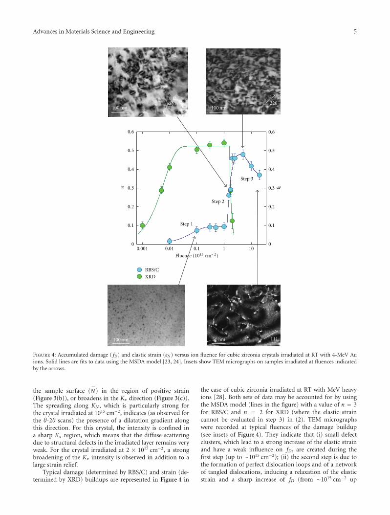
Advances in Materials Science and Engineering 5
111
220 220
Fluence (1015 cm− 2)
0.001 0.01 0.1 1 10
f D
0
0.1
0.2
0.3
0.4
0.5
0.6
N
0
0.1
0.2
0.3
0.4
0.5
0.6
XRD
RBS/C
50 nm
100 nm 100 nm
100 nm
Step 1
Step 2
Step 3
Figure 4: Accumulated damage ( fD) and elastic strain (εN ) versus ion fluence for cubic zirconia crystals irradiated at RT with 4-MeV Auions. Solid lines are fits to data using the MSDA model [23, 24]. Insets show TEM micrographs on samples irradiated at fluences indicatedby the arrows.
the sample surface (⇀N) in the region of positive strain
(Figure 3(b)), or broadens in the Kx direction (Figure 3(c)).The spreading along KN , which is particularly strong forthe crystal irradiated at 1015 cm−2, indicates (as observed forthe θ-2θ scans) the presence of a dilatation gradient alongthis direction. For this crystal, the intensity is confined ina sharp Kx region, which means that the diffuse scatteringdue to structural defects in the irradiated layer remains veryweak. For the crystal irradiated at 2 × 1015 cm−2, a strongbroadening of the Kx intensity is observed in addition to alarge strain relief.
Typical damage (determined by RBS/C) and strain (de-termined by XRD) buildups are represented in Figure 4 in
the case of cubic zirconia irradiated at RT with MeV heavyions [28]. Both sets of data may be accounted for by usingthe MSDA model (lines in the figure) with a value of n = 3for RBS/C and n = 2 for XRD (where the elastic straincannot be evaluated in step 3) in (2). TEM micrographswere recorded at typical fluences of the damage buildup(see insets of Figure 4). They indicate that (i) small defectclusters, which lead to a strong increase of the elastic strainand have a weak influence on fD, are created during thefirst step (up to ∼1015 cm−2); (ii) the second step is due tothe formation of perfect dislocation loops and of a networkof tangled dislocations, inducing a relaxation of the elasticstrain and a sharp increase of fD (from ∼1015 cm−2 up

6 Advances in Materials Science and Engineering
(dpa)
1 10
Acc
um
ula
ted
dam
age
(fD
)
0
0.2
0.4
0.6
0.8
ZrO2
MgAl2O4
UO2
(a)
Acc
um
ula
ted
dam
age
(fD
)
0
0.2
0.4
0.6
0.8
1
(dpa)
0.1 1
SiCGd2Ti2O7
(b)
Figure 5: Accumulated damage ( fD) versus ion fluence for nonamorphizable (a) and amorphizable (b) ceramics irradiated at RT with slowions. Insets show TEM diffraction patterns recorded at the final fluences on both types of materials.
to ∼ 5 × 1015 cm−2); (iii) long dislocations, which inducea reorganization of the crystal, leading to a decrease of fD,are exhibited in step 3 (above ∼ 5 × 1015 cm−2). A similarbehavior (except step 3) was observed in cubic zirconiairradiated with a large variety of slow ions [29], leading tothe conclusion that the number of displacements per atomof the target (dpa) is the key parameter for the evolution ofthe damage buildup in the nuclear collision regime.
Figure 5 compares the damage buildups (expressed indpa), as determined by RBS/C, obtained for nonamor-phizable (spinel, zirconia, and urania; Figure 5(a)) andamorphizable (titanate pyrochlore and silicon carbide;Figure 5(b)) ceramics irradiated with slow ions [30–35].It is worth mentioning that the shape of the damagekinetics may slightly differ depending on the irradiationconditions. Nevertheless, the damage accumulation processalways occurs in several damage steps, so that RBS/C datamay be accounted for by using the MSDA model (lines inthe figure) with n ≥ 2 in (2) for all materials. It must benoted that, except when the implanted impurities play a rolein the damage process (e.g., noble gases or Cs [29]), theexistence of a third step was only observed in cubic zirconia(ZrO2) and magnesia (not shown on the figure for the sake ofclarity). Nevertheless, some data at very high fluence may bemissing for the observation of this third stage (for instancefor MgAl2O4 and UO2). The insets show TEM diffractionpatterns recorded at the end of irradiation, which indicatethat the samples either remain crystalline (Figure 5(a)) orare amorphized (Figure 5(b)) upon slow ion irradiation. Itis worthwhile to mention that the value of fD at the end ofthe second step of the damage accumulation cannot be takenas a reliable evaluation of the damage level in the crystal inthe case of nonamorphizable materials (Figure 5(a)), sincethis value depends on the geometry of radiation defects
via dechanneling effects inherent to the RBS/C technique.Conversely, the dose (Φ2) at which step 2 starts, leadingeither to the formation of dislocation loops (in zirconia orurania) or to amorphization (in titanate pyrochlore or siliconcarbide), is a parameter that can be used as an indicator ofthe stability of materials upon ion irradiation: the highestΦ2, the greatest resistance to disordering or amorphization.It is worth mentioning that, for the materials selected inthis study, the hierarchy is maintained irrespective of theirradiation conditions.
4. Effects of Electronic Excitation (Swift Ions)
The structure of latent tracks created in the wake of swiftions is dependent on both the ion mass (through theenergy density deposited in electronic excitations) and theinvestigated material (insulators are generally more sensitiveto Se than semiconductors or metals).
Example of RBS/C spectra obtained for cubic zirconiacrystals irradiated at RT with GeV heavy ions at variousfluences is provided in Figure 6(a). Spectra registered inrandom and 〈100〉-axial directions on a virgin crystalare very similar to those shown in Figure 2(a). However,in contrast to Figure 2(a), no bump is observed around2100 keV for spectra recorded in the 〈100〉-axial directionon irradiated crystals. Irradiation leads to an increase withincreasing ion fluence of the Zr yield in the whole analyzedthickness, with the presence of additional disorder in thenear-surface region of crystals, that is, around 2600 keV.RBS/C spectra of Figure 6(a) cannot be fitted with a simpledecomposition method since they do not reveal the presenceof damage peaks (as in Figure 2(a)), but rather exhibitprogressive dechanneling. In such cases, the use of Monte-Carlo simulations (solid lines) performed with the McChasy
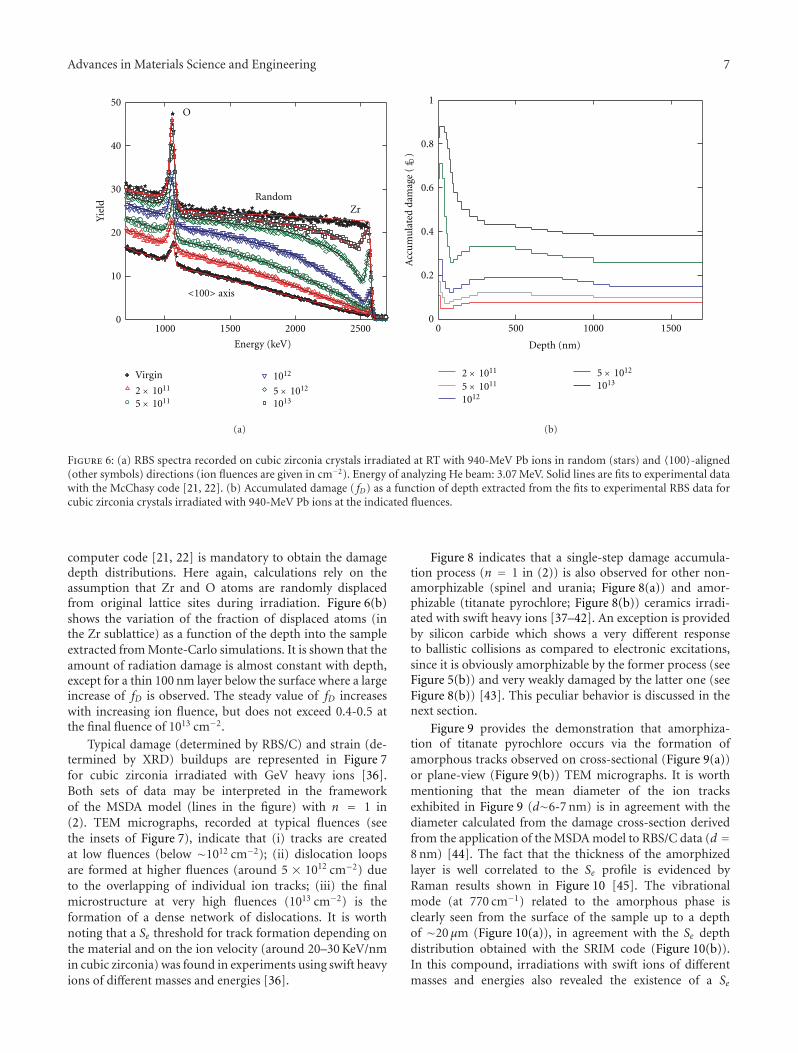
Advances in Materials Science and Engineering 7
0
10
20
30
40
50Y
ield
1000 1500 2000 2500
Energy (keV)
RandomZr
O
Virgin
2 × 10¹¹
5 × 10¹¹
1012
5 × 10¹²
1013
<100> axis
(a)
0
0.2
0.4
0.6
0.8
1
0 500 1000 1500
Depth (nm)
Acc
um
ula
ted
dam
age
(fD
)
2 × 10¹¹
5 × 10¹¹
1012
5 × 10¹²
1013
(b)
Figure 6: (a) RBS spectra recorded on cubic zirconia crystals irradiated at RT with 940-MeV Pb ions in random (stars) and 〈100〉-aligned(other symbols) directions (ion fluences are given in cm−2). Energy of analyzing He beam: 3.07 MeV. Solid lines are fits to experimental datawith the McChasy code [21, 22]. (b) Accumulated damage ( fD) as a function of depth extracted from the fits to experimental RBS data forcubic zirconia crystals irradiated with 940-MeV Pb ions at the indicated fluences.
computer code [21, 22] is mandatory to obtain the damagedepth distributions. Here again, calculations rely on theassumption that Zr and O atoms are randomly displacedfrom original lattice sites during irradiation. Figure 6(b)shows the variation of the fraction of displaced atoms (inthe Zr sublattice) as a function of the depth into the sampleextracted from Monte-Carlo simulations. It is shown that theamount of radiation damage is almost constant with depth,except for a thin 100 nm layer below the surface where a largeincrease of fD is observed. The steady value of fD increaseswith increasing ion fluence, but does not exceed 0.4-0.5 atthe final fluence of 1013 cm−2.
Typical damage (determined by RBS/C) and strain (de-termined by XRD) buildups are represented in Figure 7for cubic zirconia irradiated with GeV heavy ions [36].Both sets of data may be interpreted in the frameworkof the MSDA model (lines in the figure) with n = 1 in(2). TEM micrographs, recorded at typical fluences (seethe insets of Figure 7), indicate that (i) tracks are createdat low fluences (below ∼1012 cm−2); (ii) dislocation loopsare formed at higher fluences (around 5 × 1012 cm−2) dueto the overlapping of individual ion tracks; (iii) the finalmicrostructure at very high fluences (1013 cm−2) is theformation of a dense network of dislocations. It is worthnoting that a Se threshold for track formation depending onthe material and on the ion velocity (around 20–30 KeV/nmin cubic zirconia) was found in experiments using swift heavyions of different masses and energies [36].
Figure 8 indicates that a single-step damage accumula-tion process (n = 1 in (2)) is also observed for other non-amorphizable (spinel and urania; Figure 8(a)) and amor-phizable (titanate pyrochlore; Figure 8(b)) ceramics irradi-ated with swift heavy ions [37–42]. An exception is providedby silicon carbide which shows a very different responseto ballistic collisions as compared to electronic excitations,since it is obviously amorphizable by the former process (seeFigure 5(b)) and very weakly damaged by the latter one (seeFigure 8(b)) [43]. This peculiar behavior is discussed in thenext section.
Figure 9 provides the demonstration that amorphiza-tion of titanate pyrochlore occurs via the formation ofamorphous tracks observed on cross-sectional (Figure 9(a))or plane-view (Figure 9(b)) TEM micrographs. It is worthmentioning that the mean diameter of the ion tracksexhibited in Figure 9 (d∼6-7 nm) is in agreement with thediameter calculated from the damage cross-section derivedfrom the application of the MSDA model to RBS/C data (d =8 nm) [44]. The fact that the thickness of the amorphizedlayer is well correlated to the Se profile is evidenced byRaman results shown in Figure 10 [45]. The vibrationalmode (at 770 cm−1) related to the amorphous phase isclearly seen from the surface of the sample up to a depthof ∼20 μm (Figure 10(a)), in agreement with the Se depthdistribution obtained with the SRIM code (Figure 10(b)).In this compound, irradiations with swift ions of differentmasses and energies also revealed the existence of a Se
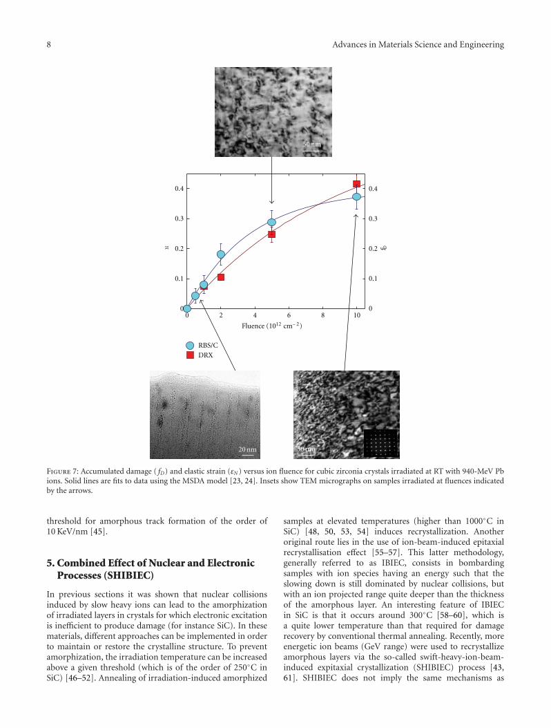
8 Advances in Materials Science and Engineering
Fluence (1012 cm− 2)
0 2 4 6 8 10
N
0
0.1
0.2
0.3
0.4
f D
0
0.1
0.2
0.3
0.4
RXD
RBS/C
50 nm20 nm
50 nm
Figure 7: Accumulated damage ( fD) and elastic strain (εN ) versus ion fluence for cubic zirconia crystals irradiated at RT with 940-MeV Pbions. Solid lines are fits to data using the MSDA model [23, 24]. Insets show TEM micrographs on samples irradiated at fluences indicatedby the arrows.
threshold for amorphous track formation of the order of10 KeV/nm [45].
5. Combined Effect of Nuclear and ElectronicProcesses (SHIBIEC)
In previous sections it was shown that nuclear collisionsinduced by slow heavy ions can lead to the amorphizationof irradiated layers in crystals for which electronic excitationis inefficient to produce damage (for instance SiC). In thesematerials, different approaches can be implemented in orderto maintain or restore the crystalline structure. To preventamorphization, the irradiation temperature can be increasedabove a given threshold (which is of the order of 250◦C inSiC) [46–52]. Annealing of irradiation-induced amorphized
samples at elevated temperatures (higher than 1000◦C inSiC) [48, 50, 53, 54] induces recrystallization. Anotheroriginal route lies in the use of ion-beam-induced epitaxialrecrystallisation effect [55–57]. This latter methodology,generally referred to as IBIEC, consists in bombardingsamples with ion species having an energy such that theslowing down is still dominated by nuclear collisions, butwith an ion projected range quite deeper than the thicknessof the amorphous layer. An interesting feature of IBIECin SiC is that it occurs around 300◦C [58–60], which isa quite lower temperature than that required for damagerecovery by conventional thermal annealing. Recently, moreenergetic ion beams (GeV range) were used to recrystallizeamorphous layers via the so-called swift-heavy-ion-beam-induced expitaxial crystallization (SHIBIEC) process [43,61]. SHIBIEC does not imply the same mechanisms as

Advances in Materials Science and Engineering 9
Ion fluence (1012 cm− 2)
0 2 4 6 8 10
Acc
um
ula
ted
dam
age
(fD
)
0
0.2
0.4
0.6
MgAl2O4
ZrO2
UO2
(a)
Ion fluence (1012 cm− 2)
0 2 4 6 8 10
Acc
um
ula
ted
dam
age
(fD
)
0
0.2
0.4
0.6
0.8
1
Gd2Ti2O7
SiC
(b)
Figure 8: Accumulated damage ( fD) versus ion fluence for nonamorphizable (a) and amorphizable (b) ceramics irradiated at RT with swiftions. The inset shows a TEM diffraction pattern recorded at the final fluence on Gd2Ti2O7.
50 nm
(a)
5 nm
(b)
Figure 9: TEM micrographs recorded on a Gd2Ti2O7 crystal irradiated at RT with 870 MeV Xe ions at 2× 1011 cm−2. (a) Cross-section; (b)plane view with a higher magnification.
those prevailing during IBIEC at low energy, but seemsto be more efficient in that sense that the temperature atwhich recrystallization occurs is lowered as compared to thatrequired for IBIEC.
A SHIBIEC experiment generally involves two sequences:(i) preirradiation with slow ions leading to the progressiveformation of a shallow amorphous layer; (ii) postirradiationwith swift ions inducing epitaxial recrystallization by elec-tronic energy loss of the layer which was previously amor-phized by nuclear collisions. Figure 11 shows an example ofSHIBIEC monitored by RBS/C in the case of silicon carbide[62]. Irradiation of SiC crystals with slow Fe ions leads to theformation of an amorphous layer (the aligned signal reachesthe random level: Figure 11(a)) in a 20–40 nm depth range(Figure 11(b)). Subsequent irradiation of the same samplewith swift Pb ions induces a decrease of the aligned yield
with increasing ion fluence (Figure 11(a)), which indicatesa partial recrystallization of the amorphized layer (see alsothe decrease of fD in Figure 11(b)). Results are summarizedin Figure 12 that shows (i) the amorphization buildup dueto slow Fe ion irradiation exhibiting a two-step process [63],and (ii) the SHIBIEC effect at different Fe fluences, whichleads to a clear decrease of fD. It is worth noting that anincrease of the temperature at which swift heavy ion post-irradiation is performed leads to an enhancement of theSHIBIEC process.
6. Conclusion
Energetic ions in the KeV-GeV range can be used to simulatethe radiations produced in nuclear reactors or in storageforms. From a fundamental viewpoint, ion irradiations allow
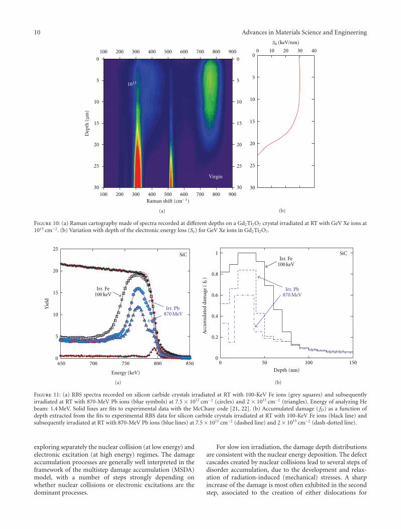
10 Advances in Materials Science and Engineering
Virgin
1013
100 200 300 400 500 600 700 800 900
100 200 300 400 500 600 700 800 900
Raman shift (cm− 1)
30
25
20
15
10
5
0
30
25
20
15
10
5
0
Dep
th(μ
m)
(a)
30
25
20
15
10
5
00 10 20 30 40
Se (keV/nm)
(b)
Figure 10: (a) Raman cartography made of spectra recorded at different depths on a Gd2Ti2O7 crystal irradiated at RT with GeV Xe ions at1013 cm−2. (b) Variation with depth of the electronic energy loss (Se) for GeV Xe ions in Gd2Ti2O7.
0
5
10
15
20
25
Yie
ld
Energy (keV)
650 700 750 800 850
SiC
Irr. Fe100 keV
Irr. Pb870 MeV
(a)
0
0.2
0.4
0.6
0.8
1
0 50 100 150
Depth (nm)
SiC
Acc
um
ula
ted
dam
age
(fD
)
Irr. Fe100 keV
Irr. Pb870 MeV
(b)
Figure 11: (a) RBS spectra recorded on silicon carbide crystals irradiated at RT with 100-KeV Fe ions (grey squares) and subsequentlyirradiated at RT with 870-MeV Pb ions (blue symbols) at 7.5 × 1012 cm−2 (circles) and 2 × 1013 cm−2 (triangles). Energy of analyzing Hebeam: 1.4 MeV. Solid lines are fits to experimental data with the McChasy code [21, 22]. (b) Accumulated damage ( fD) as a function ofdepth extracted from the fits to experimental RBS data for silicon carbide crystals irradiated at RT with 100-KeV Fe ions (black line) andsubsequently irradiated at RT with 870-MeV Pb ions (blue lines) at 7.5× 1012 cm−2 (dashed line) and 2× 1013 cm−2 (dash-dotted line).
exploring separately the nuclear collision (at low energy) andelectronic excitation (at high energy) regimes. The damageaccumulation processes are generally well interpreted in theframework of the multistep damage accumulation (MSDA)model, with a number of steps strongly depending onwhether nuclear collisions or electronic excitations are thedominant processes.
For slow ion irradiation, the damage depth distributionsare consistent with the nuclear energy deposition. The defectcascades created by nuclear collisions lead to several steps ofdisorder accumulation, due to the development and relax-ation of radiation-induced (mechanical) stresses. A sharpincrease of the damage is most often exhibited in the secondstep, associated to the creation of either dislocations for

Advances in Materials Science and Engineering 11
0
0.2
0.4
0.6
0.8
1
0.5 1 2 5
SiC
Acc
um
ula
ted
dam
age
(fD
)
Fluence (1014 cm− 2)
Figure 12: Accumulated damage ( fD) versus ion fluence for silicon carbide crystals irradiated at RT with 100 keV Fe ions (squares), andsubsequently irradiated at RT (at 2× 1013 cm−2) with 870 MeV Pb ions (circles). The solid line is a fit to Fe irradiation data using the MSDAmodel [23, 24].
nonamorphizable materials, or amorphous layers in the caseof amorphizable materials. The dose (in dpa) at which thissecond step occurs may be used as an indicator of theradiation resistance of materials.
For swift ion irradiation, the damage depth distributionsare consistent with the electronic energy loss. Tracks createdby electronic excitation cause a direct transformation ofthe melt volume into a new structure via a single-stepprocess. The overlapping of tracks at high fluences leads tothe formation of either dislocations or amorphous layers.Saturation of the damage is observed at fluences at least oneorder of magnitude lower than those required to obtain thesame amount of disorder in the case of slow ion irradiation.Results also show the existence of Se thresholds for trackformation, which depend on the materials properties.
Amorphous layers formed by slow ion irradiation canbe recrystallized by swift ion irradiation (SHIBIEC). Thiseffect differs from the well-known IBIEC process by thefact that it does not require the assistance of an externalheating source. It is related to the energy deposited by theincoming ions into the target electrons and can thereforebe interpreted in the framework of thermal spike models.Besides the fact that the SHIBIEC process is important froma fundamental viewpoint, it presents a crucial interest forindustrial applications, particularly concerning the operatingcycle of nuclear reactors of the next generations. Actually,amorphization due to irradiations with neutrons or heavyions arising from the alpha-decay of actinides can bedetrimental to the physical integrity of a material. However,a balance between amorphization and damage recovery bySHIBIEC may well occur in order to preserve the crystallinityof irradiated nuclear materials, since swift ions (i.e., fissionfragments) are also generated in nuclear fuels.
The investigation of the synergy between radiation effectsinduced simultaneously by slow and swift ions offers interest-ing prospects in this research field. Such a daunting challenge
is reachable by the development of dedicated new facilitiesable to deliver several ion beams in a unique irradiationchamber, such as the JANNUS platform recently operatingin the Orsay-Saclay area.
Acknowledgments
This work was partially financed by the GNR MATINEX. Theexperimental program also benefited from grants providedby the French-Polish cooperation Program no. 01–104.
References
[1] Hj. Matzke, “Radiation damage in crystalline insulators,oxides and ceramic nuclear fuels,” Radiation Effects, vol. 64,no. 1–4, pp. 3–33, 1981.
[2] L. W. Hobbs, F. W. Clinard Jr., S. J. Zinkle, and R. C. Ewing,“Radiation effects in ceramics,” Journal of Nuclear Materials,vol. 216, pp. 291–321, 1994.
[3] R. C. Ewing, W. J. Weber, and F. W. Clinard Jr., “Radiationeffects in nuclear waste forms for high-level radioactive waste,”Progress in Nuclear Energy, vol. 29, no. 2, pp. 63–127, 1995.
[4] S. J. Zinkle and C. Kinoshita, “Defect production in ceramics,”Journal of Nuclear Materials, vol. 251, pp. 200–217, 1997.
[5] C. J. McHargue, “Ion beam modification of ceramics,” Mate-rials Science and Engineering A, vol. 253, no. 1-2, pp. 94–105,1998.
[6] W. J. Weber, R. C. Ewing, C. R. A. Catlow et al., “Radiationeffects in crystalline ceramics for the immobilization of high-level nuclear waste and plutonium,” Journal of MaterialsResearch, vol. 13, no. 6, pp. 1434–1484, 1998.
[7] W. L. Gong, W. Lutze, and R. C. Ewing, “Zirconia ceramicsfor excess weapons plutonium waste,” Journal of NuclearMaterials, vol. 277, no. 2-3, pp. 239–249, 2000.
[8] L. Thome and F. Garrido, “Application of ion beams to nuclearwaste issues: evaluation of nuclear ceramics,” Vacuum, vol. 63,no. 4, pp. 619–626, 2001.

12 Advances in Materials Science and Engineering
[9] R. C. Ewing, W. J. Weber, and J. Lian, “Nuclear wastedisposal-pyrochlore (A2B2O7): nuclear waste form for theimmobilization of plutonium and “minor” actinides,” Journalof Applied Physics, vol. 95, no. 11, pp. 5949–5971, 2004.
[10] J. Lian, L. M. Wang, K. Sun, and R. C. Ewing, “In situ TEMof radiation effects in complex ceramics,” Microscopy Researchand Technique, vol. 72, no. 3, pp. 165–181, 2009.
[11] D. A. Thompson, “High density cascade effects,” RadiationEffects, vol. 56, no. 3-4, pp. 105–150, 1981.
[12] See the Proceedings of the 8th International Symposium on SwiftHeavy Ions in Matter (SHIM ’09), Nuclear Instruments andMethods in Physics Research Section B, vol. 267, 2009.
[13] F. Seitz and J. S. Koehler, “Displacement of atoms duringradiation,” in Solid State Physics: Advances in Research andApplications, F. Seitz and D. Turnbull, Eds., pp. 305–448,Academic Press , New York, NY, USA, 1956.
[14] M. Toulemonde, C. Dufour, and E. Paumier, “Transient ther-mal process after a high-energy heavy-ion irradiation ofamorphous metals and semiconductors,” Physical Review B,vol. 46, no. 22, pp. 14362–14369, 1992.
[15] G. Szenes, “General features of latent track formation inmagnetic insulators irradiated with swift heavy ions,” PhysicalReview B, vol. 51, no. 13, pp. 8026–8029, 1995.
[16] H. Trinkaus and A. I. Ryazanov, “Viscoelastic model for theplastic flow of amorphous solids under energetic ion bom-bardment,” Physical Review Letters, vol. 74, no. 25, pp. 5072–5075, 1995.
[17] R. L. Fleischer, P. B. Price, and R. M. Walker, “Ion explosionspike mechanism for formation of charged-particle tracks insolids,” Journal of Applied Physics, vol. 36, no. 11, pp. 3645–3652, 1965.
[18] L. E. Seiberling, J. E. Griffith, and T. A. Tombrello, “Athermalized ion explosion model for high energy sputteringand track,” Radiation effects, vol. 52, no. 3-4, pp. 201–210,1980.
[19] D. Lesueur and A. Dunlop, “Damage creation via electronicexcitations in metallic targets: theoretical model,” RadiationEffects and Defects in Solids, vol. 126, p. 105, 1993.
[20] J. F. Gibbons, “Ion implantation in semiconductors—part II:damage production and annealing,” Proceedings of the IEEE,vol. 60, no. 9, pp. 1062–1096, 1972.
[21] L. Nowicki, Damage production in cubic zirconia irradiatedwith swift heavy ions, Ph.D. thesis, The Andrzej Soltan Institutefor Nuclear Studies, Warsaw, Poland, 1997.
[22] L. Nowicki, A. Turos, R. Ratajczak, A. Stonert, and F. Garrido,“Modern analysis of ion channeling data by Monte Carlosimulations,” Nuclear Instruments and Methods in PhysicsResearch, Section B, vol. 240, no. 1-2, pp. 277–282, 2005.
[23] J. Jagielski and L. Thome, “Multi-step damage accumulation inirradiated crystals,” Applied Physics A, vol. 97, no. 1, pp. 147–155, 2009.
[24] J. Jagielski and L. Thome, “Discontinuous character of thedamage build-up in the elastic collision regime,” RadiationEffects and Defects in Solids, vol. 166, no. 5, pp. 367–372, 2011.
[25] J. R. Tesmer and M. Nastasi, Eds., Handbook of ModernIon Beam Materials Analysis, Materials Research Society,Pittsburgh, Pa, USA, 1995.
[26] L. Thome, A. Gentils, J. Jagielski, S. E. Enescu, and F. Garrido,“On the use of the 16O(4He,4He) 16O resonance for theevaluation of radiation damage in oxides,” Nuclear Instrumentsand Methods in Physics Research, Section B, vol. 219-220, no. 1–4, pp. 99–104, 2004.
[27] A. Boulle and A. Debelle, “Strain-profile determination inion-implanted single crystals using generalized simulatedannealing,” Journal of Applied Crystallography, vol. 43, no. 5,pp. 1046–1052, 2010.
[28] S. Moll, L. Thome, G. Sattonnay et al., “Multistep damageevolution process in cubic zirconia irradiated with MeV ions,”Journal of Applied Physics, vol. 106, no. 7, Article ID 073509,2009.
[29] L. Thome, J. Fradin, J. Jagielski, A. Gentils, S. E. Enescu, and F.Garrido, “Radiation damage in ion-irradiated yttria-stabilizedcubic zirconia single crystals,” EPJ Applied Physics, vol. 24, no.1, pp. 37–48, 2003.
[30] F. Garrido, C. Choffel, J. C. Dran, L. Thome, L. Nowicki,and A. Turos, “Structural modifications in uranium dioxideirradiated with swift heavy ions,” Nuclear Instruments andMethods in Physics Research, Section B, vol. 127-128, pp. 634–638, 1997.
[31] S. E. Enescu, L. Thome, A. Gentils, and T. Thome, “High-temperature annealing behavior of ion-implanted spinel sin-gle crystals,” Journal of Materials Research, vol. 19, no. 12, pp.3463–3473, 2004.
[32] A. Gentils, S. E. Enescu, L. Thome, H. Khodja, G. Blaise,and T. Thome, “High-temperature stability of ion-implantedzirconia and spinel,” Journal of Applied Physics, vol. 97, no. 11,Article ID 113509, 6 pages, 2005.
[33] F. Garrido, L. Vincent, L. Nowicki, G. Sattonnay, and L.Thome, “Radiation stability of fluorite-type nuclear oxides,”Nuclear Instruments and Methods in Physics Research, SectionB, vol. 266, no. 12-13, pp. 2842–2847, 2008.
[34] A. Audren, A. Benyagoub, L. Thome, and F. Garrido, “Ionimplantation of iodine into silicon carbide: influence oftemperature on the produced damage and on the diffusionbehaviour,” Nuclear Instruments and Methods in PhysicsResearch, Section B, vol. 266, no. 12-13, pp. 2810–2813, 2008.
[35] Y. Zhang, J. Jagielski, I. T. Bae et al., “Damage evolution in Au-implanted Ho2Ti2O7 titanate pyrochlore,” Nuclear Instrumentsand Methods in Physics Research, Section B, vol. 268, no. 19, pp.3009–3013, 2010.
[36] S. Moll, L. Thome, L. Vincent et al., “Damage inducedby electronic excitation in ion-irradiated yttria-stabilizedzirconia,” Journal of Applied Physics, vol. 105, no. 2, Article ID023512, 2009.
[37] L. Thome, J. Jagielski, A. Gentils, L. Nowicki, and F. Garrido,“Quantitative analysis of radiation-induced disorder in spinelcrystals,” Nuclear Instruments and Methods in Physics Research,Section B, vol. 242, no. 1-2, pp. 643–645, 2006.
[38] L. Thome, A. Gentils, J. Jagielski, F. Garrido, and T. Thome,“Physicochemical modifications induced by ion bombard-ment and thermal treatments in zirconia and spinel,” NuclearInstruments and Methods in Physics Research, Section B, vol.250, no. 1-2, pp. 106–113, 2006.
[39] L. Thome, A. Gentils, J. Jagielski, F. Garrido, and T. Thome,“Radiation stability of ceramics: test cases of zirconia andspinel,” Vacuum, vol. 81, no. 10, pp. 1264–1270, 2007.
[40] G. Sattonnay, S. Moll, L. Thome et al., “Heavy-ion irradiationof pyrochlore oxides: comparison between low and highenergy regimes,” Nuclear Instruments and Methods in PhysicsResearch, Section B, vol. 266, no. 12-13, pp. 3043–3047, 2008.
[41] F. Garrido, S. Moll, G. Sattonnay, L. Thome, and L. Vincent,“Radiation tolerance of fluorite-structured oxides subjected toswift heavy ion irradiation,” Nuclear Instruments and Methodsin Physics Research, Section B, vol. 267, no. 8-9, pp. 1451–1455,2009.
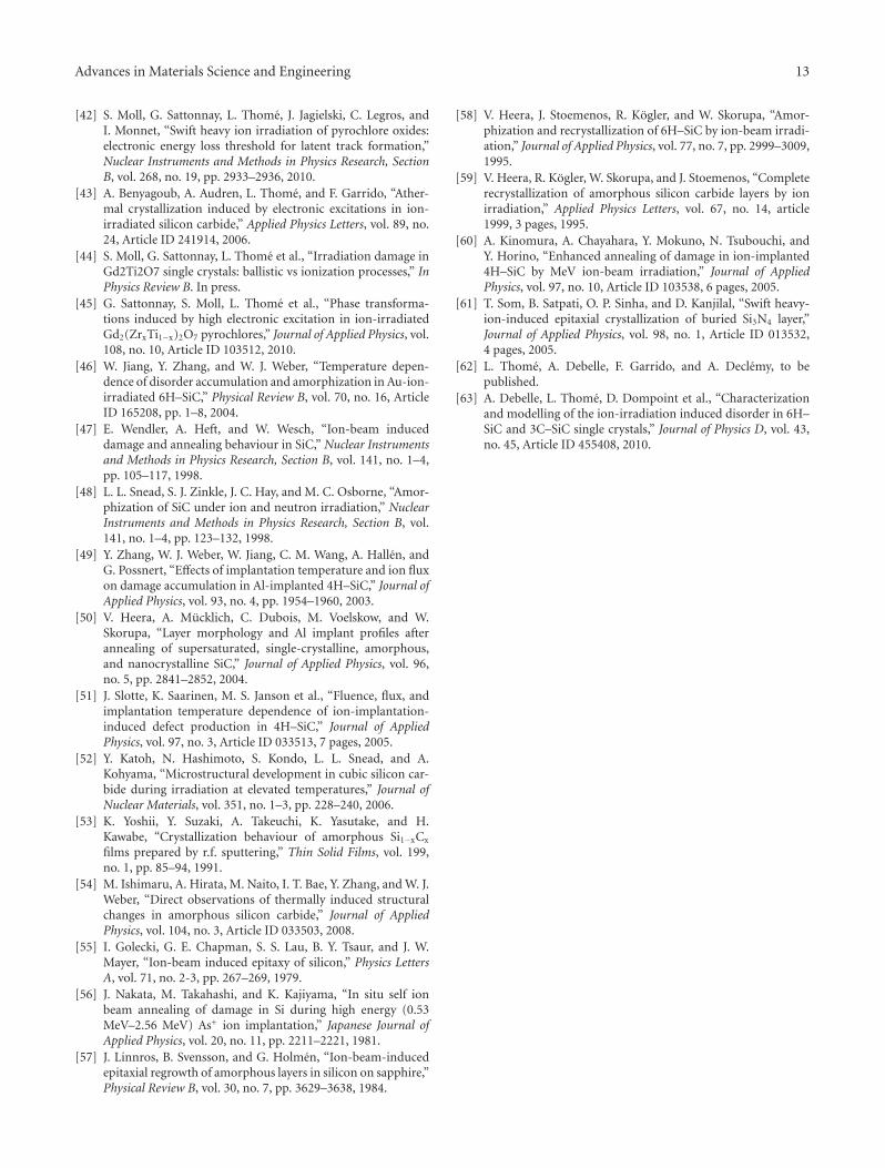
Advances in Materials Science and Engineering 13
[42] S. Moll, G. Sattonnay, L. Thome, J. Jagielski, C. Legros, andI. Monnet, “Swift heavy ion irradiation of pyrochlore oxides:electronic energy loss threshold for latent track formation,”Nuclear Instruments and Methods in Physics Research, SectionB, vol. 268, no. 19, pp. 2933–2936, 2010.
[43] A. Benyagoub, A. Audren, L. Thome, and F. Garrido, “Ather-mal crystallization induced by electronic excitations in ion-irradiated silicon carbide,” Applied Physics Letters, vol. 89, no.24, Article ID 241914, 2006.
[44] S. Moll, G. Sattonnay, L. Thome et al., “Irradiation damage inGd2Ti2O7 single crystals: ballistic vs ionization processes,” InPhysics Review B. In press.
[45] G. Sattonnay, S. Moll, L. Thome et al., “Phase transforma-tions induced by high electronic excitation in ion-irradiatedGd2(ZrxTi1−x)2O7 pyrochlores,” Journal of Applied Physics, vol.108, no. 10, Article ID 103512, 2010.
[46] W. Jiang, Y. Zhang, and W. J. Weber, “Temperature depen-dence of disorder accumulation and amorphization in Au-ion-irradiated 6H–SiC,” Physical Review B, vol. 70, no. 16, ArticleID 165208, pp. 1–8, 2004.
[47] E. Wendler, A. Heft, and W. Wesch, “Ion-beam induceddamage and annealing behaviour in SiC,” Nuclear Instrumentsand Methods in Physics Research, Section B, vol. 141, no. 1–4,pp. 105–117, 1998.
[48] L. L. Snead, S. J. Zinkle, J. C. Hay, and M. C. Osborne, “Amor-phization of SiC under ion and neutron irradiation,” NuclearInstruments and Methods in Physics Research, Section B, vol.141, no. 1–4, pp. 123–132, 1998.
[49] Y. Zhang, W. J. Weber, W. Jiang, C. M. Wang, A. Hallen, andG. Possnert, “Effects of implantation temperature and ion fluxon damage accumulation in Al-implanted 4H–SiC,” Journal ofApplied Physics, vol. 93, no. 4, pp. 1954–1960, 2003.
[50] V. Heera, A. Mucklich, C. Dubois, M. Voelskow, and W.Skorupa, “Layer morphology and Al implant profiles afterannealing of supersaturated, single-crystalline, amorphous,and nanocrystalline SiC,” Journal of Applied Physics, vol. 96,no. 5, pp. 2841–2852, 2004.
[51] J. Slotte, K. Saarinen, M. S. Janson et al., “Fluence, flux, andimplantation temperature dependence of ion-implantation-induced defect production in 4H–SiC,” Journal of AppliedPhysics, vol. 97, no. 3, Article ID 033513, 7 pages, 2005.
[52] Y. Katoh, N. Hashimoto, S. Kondo, L. L. Snead, and A.Kohyama, “Microstructural development in cubic silicon car-bide during irradiation at elevated temperatures,” Journal ofNuclear Materials, vol. 351, no. 1–3, pp. 228–240, 2006.
[53] K. Yoshii, Y. Suzaki, A. Takeuchi, K. Yasutake, and H.Kawabe, “Crystallization behaviour of amorphous Si1−xCx
films prepared by r.f. sputtering,” Thin Solid Films, vol. 199,no. 1, pp. 85–94, 1991.
[54] M. Ishimaru, A. Hirata, M. Naito, I. T. Bae, Y. Zhang, and W. J.Weber, “Direct observations of thermally induced structuralchanges in amorphous silicon carbide,” Journal of AppliedPhysics, vol. 104, no. 3, Article ID 033503, 2008.
[55] I. Golecki, G. E. Chapman, S. S. Lau, B. Y. Tsaur, and J. W.Mayer, “Ion-beam induced epitaxy of silicon,” Physics LettersA, vol. 71, no. 2-3, pp. 267–269, 1979.
[56] J. Nakata, M. Takahashi, and K. Kajiyama, “In situ self ionbeam annealing of damage in Si during high energy (0.53MeV–2.56 MeV) As+ ion implantation,” Japanese Journal ofApplied Physics, vol. 20, no. 11, pp. 2211–2221, 1981.
[57] J. Linnros, B. Svensson, and G. Holmen, “Ion-beam-inducedepitaxial regrowth of amorphous layers in silicon on sapphire,”Physical Review B, vol. 30, no. 7, pp. 3629–3638, 1984.
[58] V. Heera, J. Stoemenos, R. Kogler, and W. Skorupa, “Amor-phization and recrystallization of 6H–SiC by ion-beam irradi-ation,” Journal of Applied Physics, vol. 77, no. 7, pp. 2999–3009,1995.
[59] V. Heera, R. Kogler, W. Skorupa, and J. Stoemenos, “Completerecrystallization of amorphous silicon carbide layers by ionirradiation,” Applied Physics Letters, vol. 67, no. 14, article1999, 3 pages, 1995.
[60] A. Kinomura, A. Chayahara, Y. Mokuno, N. Tsubouchi, andY. Horino, “Enhanced annealing of damage in ion-implanted4H–SiC by MeV ion-beam irradiation,” Journal of AppliedPhysics, vol. 97, no. 10, Article ID 103538, 6 pages, 2005.
[61] T. Som, B. Satpati, O. P. Sinha, and D. Kanjilal, “Swift heavy-ion-induced epitaxial crystallization of buried Si3N4 layer,”Journal of Applied Physics, vol. 98, no. 1, Article ID 013532,4 pages, 2005.
[62] L. Thome, A. Debelle, F. Garrido, and A. Declemy, to bepublished.
[63] A. Debelle, L. Thome, D. Dompoint et al., “Characterizationand modelling of the ion-irradiation induced disorder in 6H–SiC and 3C–SiC single crystals,” Journal of Physics D, vol. 43,no. 45, Article ID 455408, 2010.


![PHUL]DWLRQ XQGHU &RQWLQXRXV )ORZ …3RO\PHUL]DWLRQ UHVXOWV IRU H[SHULPHQWV LQ )LJXUH + 105 VSHFWUD RI EORFN SRO\PHUV ^ ï 0DWHULDOV DQG FKDUDFWHUL]DWLRQ PHWKRGV 0DWHULDOV 0HWK\O DFU\ODWH](https://static.fdocuments.us/doc/165x107/5fe3449e0370271e0f12d2d6/phuldwlrq-xqghu-rqwlqxrxv-orz-3rophuldwlrq-uhvxowv-iru-hshulphqwv-lq-ljxuh.jpg)
