Microstructural Evolution in Materials during Thermal...
104
Advances in Materials Science and Engineering Guest Editors: Joseph K. L. Lai, Brian Ralph, Zhiwen Chen, and Kin Ho Lo Microstructural Evolution in Materials during Thermal Processing
Transcript of Microstructural Evolution in Materials during Thermal...
Advances in Materials Science and Engineering
Guest Editors: Joseph K. L. Lai, Brian Ralph, Zhiwen Chen, and Kin Ho Lo
Microstructural Evolution in Materials during Thermal Processing
Microstructural Evolution in Materials duringThermal Processing

Advances in Materials Science and Engineering
Microstructural Evolution in Materials duringThermal Processing
Guest Editors: Joseph K. L. Lai, Brian Ralph, Zhiwen Chen,and Kin Ho Lo

Copyright © 2012 Hindawi Publishing Corporation. All rights reserved.
This is a special issue published in “Advances in Materials Science and Engineering.” All articles are open access articles distributed underthe Creative Commons Attribution License, which permits unrestricted use, distribution, and reproduction in any medium, providedthe original work is properly cited.

Editorial Board
Marcel Ausloos, BelgiumRobert S. Averback, USAV. P. S. Awana, IndiaAmit Bandyopadhyay, USAZ. Barber, UKMark Blamire, UKSusmita Bose, USASteve Bull, UKDavid Cann, USADaolun Chen, CanadaManish U. Chhowalla, USAPaolo Colombo, ItalyMartin Crimp, USAJie Dai, SingaporeC. K. Das, IndiaChris Davies, AustraliaJ. Paulo Davim, PortugalSeshu Babu Desu, USAYong Ding, USAShi Xue Dou, AustraliaChunying Duan, ChinaNadia El-Masry, USADavid Field, USAQiang Fu, ChinaJohn W. Gillespie, USAJeffrey T. Glass, USAZhennan Gu, ChinaHiroki Habazaki, JapanRichard Hennig, USA
Dachamir Hotza, BrazilChun-Hway Hsueh, USARui Huang, USAShyh-Chin Huang, TaiwanJacques Huot, CanadaHamlin Jennings, USAWilliam A. Jesser, USAA. Jorio, BrazilKazuro Kageyama, JapanS. Komarneni, USAPrashant Kumta, USAPearl Lee-Sullivan, CanadaPavel Lejcek, Czech RepublicMarkku Leskela, FinlandJun Li, SingaporeJing Li, USAYuanhua Lin, ChinaZhimin Liu, ChinaMeilin Liu, GeorgiaMaria A. Loi, The NetherlandsHai Lu, ChinaYiu-Wing Mai, AustraliaPeter Majewski, AustraliaA.-S. H. Makhlouf, GermanyR. S. Mishra, USAS. Miyazaki, JapanPaul Munroe, AustraliaKorukonda L. Murty, USALuigi Nicolais, Italy
Tsutomu Ohzuku, JapanXiaoqing Pan, USAGanapathiraman Ramanath, USARaju V. Ramanujan, SingaporeJainagesh A. Sekhar, USAYou Song, ChinaCharles C. Sorrell, AustraliaSteven L. Suib, USAWen-Hua Sun, ChinaSam-Shajing Sun, USAAchim Trampert, GermanyAn-Pang Tsai, JapanVladimir Tsukruk, USAKrystyn Van Vliet, USAStan Veprek, GermanyRui Vilar, PortugalLianzhou Wang, AustraliaKunpeng Wang, ChinaJohn Wang, SingaporeJorg M. K. Wiezorek, USAAiguo Xu, ChinaJenn-Ming Yang, USAYadong Yin, USAJihong Yu, ChinaGuan-Jun Zhang, ChinaDao Hua Zhang, SingaporeMing-Xing Zhang, Australia
Contents
Microstructural Evolution in Materials during Thermal Processing, Joseph K. L. Lai, Brian Ralph,Zhiwen Chen, and Kin Ho LoVolume 2012, Article ID 302478, 2 pages
Crystallisation Kinetics of a β-Spodumene-Based Glass Ceramic, Oscar Rubem Klegues Montedo,Dachamir Hotza, Antonio Pedro Novaes de Oliveira, Robert Meszaros, Nahum Travitzky,and Peter GreilVolume 2012, Article ID 525428, 8 pages
Formation and Device Application of Ge Nanowire Heterostructures via Rapid Thermal Annealing,Jianshi Tang, Chiu-Yen Wang, Faxian Xiu, Yi Zhou, Lih-Juann Chen, and Kang L. WangVolume 2011, Article ID 316513, 16 pages
Thermal Effect on Structure of Silver in Ion-Exchanged Soda-Lime Glasses and Aluminum-Doped ZincOxide Films, Paul W. Wang, Yanfeng Jiang, Jin-Cherng Hsu, Yu-Yun Chen, Yung-Hsing Lin,and Huang-Lu ChenVolume 2011, Article ID 987671, 7 pages
The Effects of Different Types of Fly Ash on the Compressive Strength Properties of Briquettes,Ozlem Celik Sola, Murat Yayla, Barıs Sayın, and Cengiz Duran AtisVolume 2011, Article ID 430604, 6 pages
Crystallization Behavior and Microstructural Analysis of Strontium Rich (PbxSr1−x)TiO3 GlassCeramics in Presence of La2O3, C. R. Gautam, Devendra Kumar, and Om ParkashVolume 2011, Article ID 747346, 9 pages
Crystallization Behavior and Microstructural Analysis of Lead-Rich (PbxSr1−x) TiO3 Glass CeramicsContaining 1 mole % La2O3, C. R. Gautam, Devendra Kumar, and Om ParkashVolume 2011, Article ID 402376, 11 pages
Powder Characterization and Electrochemical Properties of LiNi0.5Mn1.5O4 Cathode Materials Producedby Large Spray Pyrolysis Using Flame Combustion, Shinsuke Akao, Motofumi Yamada, Takayuki Kodera,Kenichi Myoujin, and Takashi OgiharaVolume 2011, Article ID 768143, 6 pages
Low-Temperature Strengths and Ductility of Various Tungsten Sheets, Yutaka Hiraoka andHiroaki KurishitaVolume 2011, Article ID 509457, 7 pages
Young’s Modulus and Coefficient of Linear Thermal Expansion of ZnO Conductive and TransparentUltra-Thin Films, Naoki Yamamoto, Hisao Makino, and Tetsuya YamamotoVolume 2011, Article ID 136127, 10 pages
TEM Study of High-Temperature Precipitation of Delta Phase in Inconel 718 Alloy, Moukrane Dehmas,Jacques Lacaze, Aliou Niang, and Bernard ViguierVolume 2011, Article ID 940634, 9 pages
γ′ Precipitation and Growth Kinetics in Mechanically Alloyed Ni-Al, QingXin Tang, Shigeharu Ukai,Akinobu Minami, and Shigenari HayashiVolume 2011, Article ID 137387, 7 pages
Hindawi Publishing CorporationAdvances in Materials Science and EngineeringVolume 2012, Article ID 302478, 2 pagesdoi:10.1155/2012/302478
Editorial
Microstructural Evolution in Materials duringThermal Processing
Joseph K. L. Lai,1 Brian Ralph,2 Zhiwen Chen,3 and Kin Ho Lo4
1 Department of Physics and Materials Science, City University of Hong Kong, Tat Chee Avenue, Kowloon, Hong Kong2 Brunel University, Kingston Lane, Uxbridge, UB8 3PH, UK3 School of Environmental and Chemical Engineering, Shanghai University, Shangda Road 99, P.O. Box 144, Shanghai 200444, China4 Department of Electromechanical Engineering, University of Macau, Avenida Padre Tomas Pereira, Taipa, Macau, China
Correspondence should be addressed to Joseph K. L. Lai, [email protected]
Received 16 October 2011; Accepted 16 October 2011
Copyright © 2012 Joseph K. L. Lai et al. This is an open access article distributed under the Creative Commons AttributionLicense, which permits unrestricted use, distribution, and reproduction in any medium, provided the original work is properlycited.
The study of materials science is mainly based on ourunderstanding of the relationship between microstructureand materials properties. Factors such as temperature, stress,and environment can lead to microstructural evolution witha concomitant change in properties. It is the materialsscientist’s role to harness our knowledge on this relationshipto produce materials with improved properties, or to predictthe performance of existing materials under various serviceconditions.
Over the past two decades, there have been a burgeoningnumber of novel or improved materials. This developmentis accompanied by significant advances in techniques inmaterials characterization as well as increased sophisticationin theoretical methods for the analysis of microstructures.The application of these new techniques and methodologiesto study the microstructural evolution of novel materialsoffers tremendous opportunities for scientific advancementon many fronts, with the prospect of providing new solutionsto problems which have hitherto remained intractable.
The papers published in this special issue encompassvarious materials systems: metals and alloys, glass ceramics,thin films, nanowire, and oxide powders for engineeringapplications.
The paper by Dehmas et al. reports an investigation onthe precipitate phases in Inconel 718, an important alloy forhigh temperature applications such as turbine blades. Usingtransmission electron microscopy and X-ray diffraction, theauthors were able to confirm the presence of rotation-ordered domains in δ plates and explain unexpected contrastby double diffraction due to overlapping phases.
The paper by Ukai et al. is also focused on Nickel-basedsuper-alloy for high temperature turbine applications. Thisstudy has enhanced our understanding of the precipitationand growth kinetics of γ′ and its characteristics in mechani-cally alloyed materials.
The paper by Hiraoka et al. reports the results of aninvestigation on the strength and ductility of tungsten sheetsafter various recrystallization treatments. Three-point bendtests were performed at temperatures between 290 and500 K. Fracture surfaces were examined by scanning electronmicroscopy. The mechanical properties of tungsten andmolybdenum were compared.
A glass ceramic material was studied by Montedo etal. in the their paper. The material studied is a candidatematerial for applications such as laminated tapes for screen-printed electronic components. The crystallization kineticswas studied using differential thermal analysis and scanningelectron microscopy.
Other two papers were written by the same team ofauthors. Two titanium oxide glass ceramic materials withLa2O3 addition, one strontium rich and one lead rich, werestudied. The crystallization behavior of these materials wasinvestigated using differential thermal analysis and X-raydiffraction.
Microstructural evolution during rapid thermal anneal-ing of Ge nanowires was investigated by Tang et al.in the seventh paper. Scanning electron microscopy andtransmission electron microscopy were used to observeNi2Ge/Ge/Ni2Ge nanowire heterostructures. This work has
2 Advances in Materials Science and Engineering
important implications for the future development of fieldeffect transistors.
Wang et al. present their work on zinc oxide thin filmsin the their paper. Two types of thin films were investigated:Ag ion-exchanged soda-lime glasses and aluminium-dopedZnO (AZO). Changes in chemical states and structuralmodification during and after heat treatment were explored.The results provide the basic information for determiningthe optimum heat treatment to grow silver quantum dots ofvarious size and density in thin films.
Another interesting contribution on the subject of ZnOthin films appears in one of the papers. Japanese researchersfrom the Kochi University of Technology have developed anew technique for measuring the Youngs modulus of ultra-thin films with thickness in the range of about 10 nm. Thetechnique was applied to study the mechanical properties ofGa-doped ZnO thin films, a possible substitute material forindium-tin-oxide transparent electrodes.
Another paper deals with powder materials for Lithiumion battery applications. Akao et al. from the Universityof Fukui produced LiNi0.5Mn1.5O4 cathode materials byflame combustion using a spray pyrolysis apparatus. X-ray diffraction revealed that, after calcination at 900◦C,crystalline powders with polygonal morphology and narrowparticle size distribution were obtained.
The paper by Sola et al. is concerned with a literally“down to earth” problem. For many years, scientists havebeen developing ways to make use of fly ash in order to turnit from an industrial waste with environmental and storageproblems into a useful material. The most obvious solutionto this conundrum is to use it as an additive in sinteredbriquettes in the construction industry. These authors havedetermined the effect of different types of fly ash on thecompressive strength of sintered briquettes. They showedthat sintered briquettes samples made with Tuncbilek flyash had higher percentage of glassy phase and compressivestrength.
Papers published in this special issue will be of interest tomaterials scientists and engineers who wish to extend theirknowledge on the effect of thermal processing on a broadrange of materials. We would like to take this opportunityto thank all the authors who have submitted their papers tothis publication.
Joseph K. L. LaiBrian Ralph
Zhiwen ChenKin Ho Lo
Hindawi Publishing CorporationAdvances in Materials Science and EngineeringVolume 2012, Article ID 525428, 8 pagesdoi:10.1155/2012/525428
Research Article
Crystallisation Kinetics of a β-Spodumene-Based Glass Ceramic
Oscar Rubem Klegues Montedo,1 Dachamir Hotza,2
Antonio Pedro Novaes de Oliveira,2 Robert Meszaros,3
Nahum Travitzky,3 and Peter Greil3
1 Unidade Academica de Ciencias, Engenharias e Tecnologias (UNACET), Universidade do Extremo Sul Catarinense (UNESC),88806-000 Criciuma, SC, Brazil
2 Group of Ceramic and Glass Materials (CERMAT), Department of Mechanical Engineering (EMC),Federal University of Santa Catarina (UFSC), 88040-900 Florianopolis, SC, Brazil
3 Department of Materials Science, Institute of Glass and Ceramics, University of Erlangen-Nuremberg, 91058 Erlangen, Germany
Correspondence should be addressed to Oscar Rubem Klegues Montedo, [email protected]
Received 25 February 2011; Revised 19 September 2011; Accepted 20 September 2011
Academic Editor: Joseph Lai
Copyright © 2012 Oscar Rubem Klegues Montedo et al. This is an open access article distributed under the Creative CommonsAttribution License, which permits unrestricted use, distribution, and reproduction in any medium, provided the original work isproperly cited.
LZSA (Li2O-ZrO2-SiO2-Al2O3) glass ceramic system has shown high potential to obtain LTCC laminate tapes at low sinteringtemperature (<1000◦C) for several applications, such as screen-printed electronic components. Furthermore, LZSA glass ceramicsoffer interesting mechanical, chemical, and thermal properties, which make LZSA also a potential candidate for fabricatingmultilayered structures processed by Laminated Objects Manufacturing (LOM) technology. The crystallization kinetics of anLZSA glass ceramic with a composition of 16.9Li2O·5.0ZrO2·65.1SiO2·8.6Al2O3 was investigated using nonisothermal methodsby differential thermal analysis and scanning electronic microscopy. Apparent activation energy for crystallization was found tobe in the 274–292 kJ·mol−1 range, and an Avrami parameter n of 1 was obtained that is compared very favorably with SEMobservations.
1. Introduction
A considerable effort has been spent to obtain high-per-formance glass ceramics for several potential applicationsin the medical, automotive, and telecommunication fields[1]. Low-temperature cofired ceramics (LTCCs) have createdgood perspectives for those applications, with special atten-tion to the glass ceramic materials [2, 3]. LZSA glass ceramics(Li2O-ZrO2-SiO2-Al2O3) have been studied because of theirbeneficial thermal, mechanical, and thermal properties [4],among other interesting features. Moreover, laminated LZSAbodies crystallized at 850◦C/30 min have demonstrated toexhibit a low dielectric constant of 8.61 ± 0.84 at 1 MHz(room temperature) [5]. Furthermore, their relatively lowtemperatures of sintering [6] make β-spodumene-basedglass ceramics (LZSA) a potential candidate for obtain-ing multilayered structures processed by LOM technology(Laminated Objects Manufacturing) [7]. However, the low
sintering temperature is also accomplished by low crystal-lization temperature in this system, especially for very finepowders and low heating rates. In order to control thermaltreatment for obtaining optimized properties, it is necessaryto determine the kinetics parameters of crystallization forthis glass ceramic system.
Isothermal crystallization kinetics of glass ceramic sys-tems commonly refers to the following well-establishedJohnson-Mehl-Avrami equation [8]:
− ln (1− x) = ktn, (1)
where x is the volume fraction crystallized at a giventemperature and time t, n is the Avrami parameter relatedto the nucleation and crystal growth mechanisms, and k isthe reaction rate constant related to the apparent activationenergy for crystallization, Ec. Nonisothermal conditions havebeen more largely widespread in the crystallization studies
2 Advances in Materials Science and Engineering
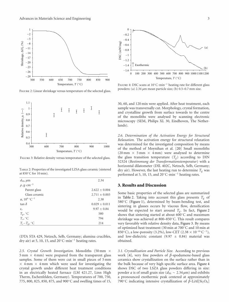
Table 1: Chemical composition of LZSA parent glass.
Oxides Glass composition, mol%
SiO2 65.1
Al2O3 8.6
Na2O 0.6
K2O 0.4
Li2O 16.9
CaO 0.6
MgO 2.0
ZrO2 5.0
BaO 0.2
ZnO 0.6
of amorphous materials [3, 9–15], despite the scepticismof Shaaban [16]. According to Shaaban [16], Kissinger plotand Ozawa plot cannot be directly used for crystallizationof amorphous materials, because crystallization is advancedby the nucleation and crystal growth process instead ofby nth order reaction. However, most of work reported inthe literature used DTA or DSC to determine the kineticsparameters Ec and n. Measurements using dilatometer werealso applied in some cases [17, 18].
Those methods, which assume that deflection from thebaseline is proportional to the instantaneous reaction rate,require a uniform temperature of the sample independentlyof the heating rate. This is obtained employing small samplesand low heating rates during heat treatments [9].
The aim of this work is to present the results of an inves-tigation about the crystallization kinetics of a β-spodumene-(LiAl [Si2O6]) based LZSA glass ceramic composition bymeans of Nonisothermal method.
2. Material and Methods
2.1. Samples Preparation. A β-spodumene-based glass ce-ramic composition with interesting chemical, thermal, andelectrical (dielectric constant) properties [4, 5] was selectedand prepared from suitable amounts of Li2CO3, ZrSiO4,SiO2, and LiAl[Si2O6] (spodumene, Colorminas Colorifıcioe Mineracao, Criciuma, Brazil). The powders were mixedand melted at 1550 ± 3◦C for 2 h in a gas furnace using amullite crucible. The melt was poured into deionized waterand the quenched frit powder was remelted at 1550 ± 2◦Cfor 2 h in an electric furnace (Nabertherm LHT 02/17 LBR,Nabertherm, Lilienthal, Germany) using an alumina crucibleto finally obtain a homogeneous viscous liquid. Chemicalanalysis is shown in Table 1. A small amount of the obtainedmelt was poured into a graphite crucible, transferred to anannealing furnace (Linn High Therm LM 421.27, Linn HighTherm, Eschenfelden, Germany) and held at 570◦C for 1 hto obtain small monoliths (50 mm × 5 mm × 4 mm) thatwere used to determine the glass transition temperature (Tg)by beam-bending test (Beam-Bending Viscosimeter, BahrThermoanalyse VIS 401, Hullhorst, Germany) applying aconstant heating rate of 10◦C·min−1. Thermal expansionwas measured with a horizontal dilatometer (DIL 402C,
4
6
8
10
12
14
16
500 600 700 800 900 1000 1100 1200
Vis
cosi
ty,μ
(dPa·s)
Temperature, T (◦C)
Annealing point (580.4◦C)
Softening point (796.4◦C)
Strain point (544.7◦C)
Melting point
(1140.5◦C)
Figure 1: Viscosity of the selected glass in function to the tem-perature.
Netzsch, Selb, Germany) at the same heating rate. Fromthe remaining glass frit a powder fraction of 0.5–0.7 mmwas prepared and subsequently dry-milled in a porcelainball mill for 3 h. The particle size was determined by lasergranulometric analysis (Cilas 1064L particle size analyzer,Orleans, France). Theoretical densities of glass powderand glass ceramic obtained at different temperatures weremeasured by He pycnometry (AccuPyc 1330, Micromeritics,Norcross, GA; 5 measurements). Apparent geometric den-sities of the compacted bodies (40 MPa, 1.4 g·cm−3 greendensity) were determined geometrically. Relative densitiesat several temperatures were calculated taking into accountthe ratio between apparent and theoretical densities ofthe heat-treated samples. Dielectric constant measurementswere carried out according to DIN 53 482/VDE 0303 ina HP Dielectric Test Fixture (16451B, Hewlett Packard,Waldhausen, Germany) at room temperature applying afrequency of 1 MHz. The samples were discs of 20 mm ×1.2 mm heat-treated at 850◦C for 10 min.
2.2. Determination of the Predominant Crystallization Mech-anism. The method of Thakur and Thiagarajan [19] wasused to determine the nucleating efficiency, in which thevariation in onset of crystallization, ΔTx, with particlesize was monitored in a differential scanning calorimeter(DSC 404C, Netzsch, Selb, Germany; alumina crucibles, dryair). A constant heating rate of 10◦C·min−1 was appliedto determine the predominant crystallization mechanism.Moreover, a small monolith sample (5 mm× 4 mm× 4 mm)was polishing to eliminate apparent surface defects andsubsequently heat-treated at 875◦C for 2 h (10◦C·min−1).
2.3. Identification of the Crystalline Phases Formed. High-temperature X-ray diffraction (HT-XRD) patterns wererecorded (Siemens D500, Siemens AG, Mannheim, Ger-many) from powdered samples. Monochromated Cu Kα1radiation was applied at a voltage of 30 kV and a current of30 mA.
2.4. Crystallisation Kinetics Investigation. The onset of crys-tallization Tc was determined by differential thermal analysis
Advances in Materials Science and Engineering 3
−29
−26
−23
−20
−17
−14
−11
−8
−5
−2
1
500 550 600 650 700 750 800 850 900
Shri
nka
ge,Δl/l o
(%)
Temperature, T (◦C)
Figure 2: Linear shrinkage versus temperature of the selected glass.
0.4
0.5
0.6
0.7
0.8
0.9
1
1.1
500 600 700 800 900 1000
Rel
ativ
e de
nsi
ty,ρ
r(—
)
Temperature, T (◦C)
Figure 3: Relative density versus temperature of the selected glass.
Table 2: Properties of the investigated LZSA glass ceramic (sinteredat 850◦C for 10 min).
d50, μm 2.34
ρ, g·cm−3
Parent glass 2.622 ± 0.004
Glass ceramic 2.711 ± 0.003
α, 106 ◦C−1 2.38
tan δ 0.029 ± 0.011
εr 9.97 ± 0.84
Tg , ◦C 580
Tc, ◦C 794
Tc−Tg , ◦C 214
(DTA STA 429, Netzsch, Selb, Germany; alumina crucibles,dry air) at 5, 10, 15, and 20◦C·min−1 heating rates.
2.5. Crystal Growth Investigation. Monoliths (50 mm ×5 mm × 4 mm) were prepared from the transparent glasssamples. Some of them were cut in small pieces of 5 mm× 4 mm × 4 mm which were used for investigating thecrystal growth under different heat treatment conditionsin an electrically heated furnace (LM 421.27, Linn HighTherm, Eschenfelden, Germany). Temperatures of 700, 750,775, 800, 825, 850, 875, and 900◦C and swelling times of 15,
−1.6
−1.4
−1.2
−1
−0.8
−0.6
−0.4
−0.2
0
0 100 200 300 400 500 600 700 800 900 1000 1100 1200
DSC
(m
W/m
g)
Temperature, T (◦C)
(b)
(a)
Exothermic
Figure 4: DSC scans at 10◦C·min−1 heating rate for different glasspowders: (a) 2.34 μm mean particle size; (b) 0.5–0.7 mm size.
30, 60, and 120 min were applied. After heat treatment, eachsample was transversally cut. Morphology, crystal formation,and crystalline growth from surface towards to the centreof the monoliths were analysed by scanning electronicmicroscopy (SEM, Philips XL 30, Eindhoven, The Nether-lands).
2.6. Determination of the Activation Energy for StructuralRelaxation. The activation energy for structural relaxationwas determined for the investigated composition by meansof the method of Moynihan et al. [20] Small monoliths(20 mm × 5 mm × 4 mm) were analyzed to determinethe glass transition temperature (Tg) according to DIN52324 (Bestimmung der Transformationstemperatur) with ahorizontal dilatometer (DIL 402C, Netzsch, Selb, Germany;dry air). However, the last heating run to determine Tg wasperformed at 5, 10, 15, and 20◦C·min−1 heating rates.
3. Results and Discussion
Some basic properties of the selected glass are summarizedin Table 2. Taking into account this glass presents Tg of580◦C (Figure 1), determined by beam-bending test, andsintering in glasses occurs by viscous flow, densificationwould be expected to start around Tg . In fact, Figure 2shows that sintering started at about 600◦C and maximumshrinkage was achieved at 800–850◦C. This result comparesvery favorably with relative density data, Figure 3. By meansof optimized heat treatment (30 min at 700◦C and 10 min at850◦C), a low-porosity (3.2%), low-CET (2.38 × 10⁻⁶◦C−1),and low-dielectric constant (9.97 ± 0.84) material wasobtained.
3.1. Crystallization and Particle Size. According to previouswork [4], very fine powders of β-spodumene-based glassceramics show crystallization on the surface rather than inthe bulk because of very high specific surface area. Figure 4shows DSC of two LSZA glass powders differing in size:powder a is of small grain size (d50 ∼ 2.34μm) and exhibitsa pronounced exothermic peak centered at approximately790◦C indicating intensive crystallization of β-LiAl[Si2O6]
4 Advances in Materials Science and Engineering
16 18 20 22 24 26 28 30 32 34 36 38 40 42
S
SS
ZS
ZS
ZS ZZ ZS ZS
Cukα 2θ (deg)
900◦C
800◦C850◦C
750◦C
650◦C700◦C
Room temperature
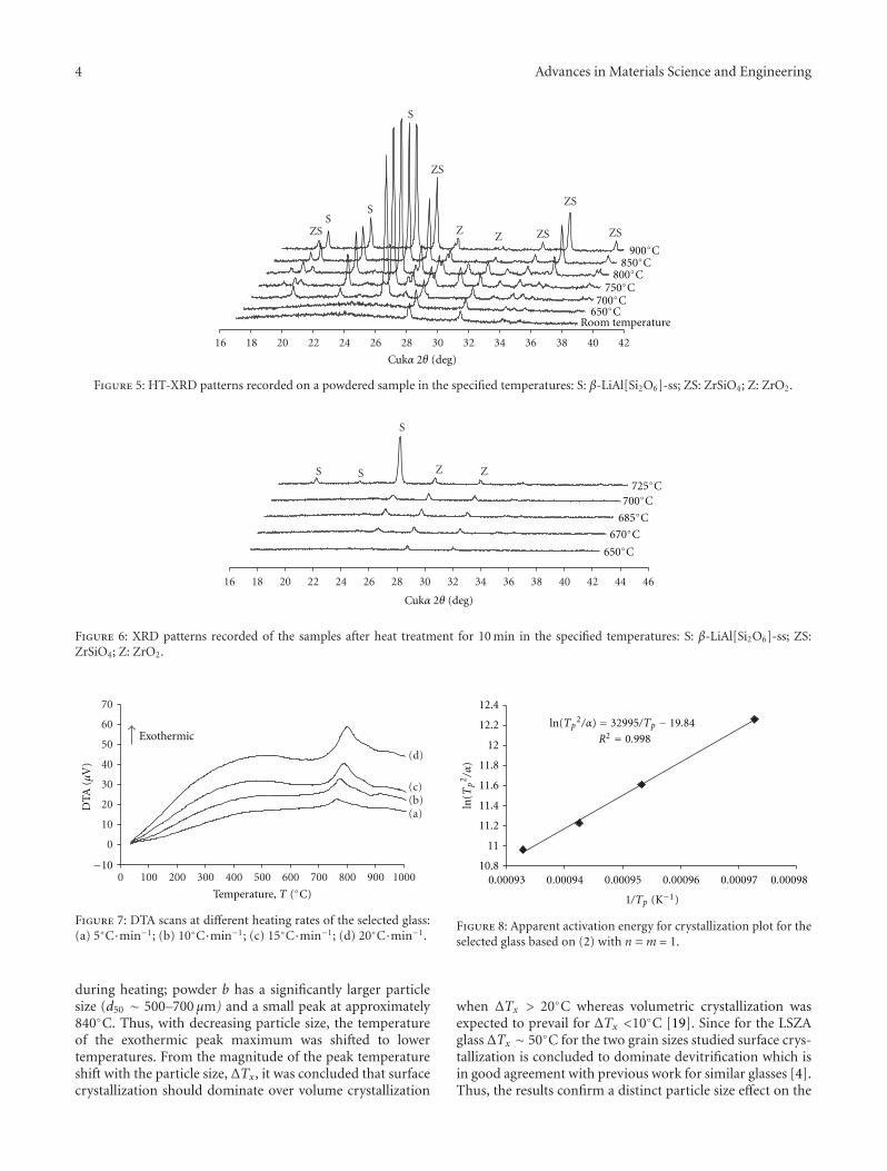
Figure 5: HT-XRD patterns recorded on a powdered sample in the specified temperatures: S: β-LiAl[Si2O6]-ss; ZS: ZrSiO4; Z: ZrO2.
16 18 20 22 24 26 28 30 32 34 36 38 40 42 44 46
Z
S
S S Z725◦C
685◦C
700◦C
670◦C
650◦C
Cukα 2θ (deg)
Figure 6: XRD patterns recorded of the samples after heat treatment for 10 min in the specified temperatures: S: β-LiAl[Si2O6]-ss; ZS:ZrSiO4; Z: ZrO2.
0
10
20
30
40
50
60
70
0 100 200 300 400 500 600 700 800 900 1000
(b)(c)
(d)
(a)
DTA
(μ
V)
−10
Temperature, T (◦C)
Exothermic
Figure 7: DTA scans at different heating rates of the selected glass:(a) 5◦C·min−1; (b) 10◦C·min−1; (c) 15◦C·min−1; (d) 20◦C·min−1.
during heating; powder b has a significantly larger particlesize (d50 ∼ 500–700 μm) and a small peak at approximately840◦C. Thus, with decreasing particle size, the temperatureof the exothermic peak maximum was shifted to lowertemperatures. From the magnitude of the peak temperatureshift with the particle size, ΔTx, it was concluded that surfacecrystallization should dominate over volume crystallization
1/Tp (K−1)
R2 = 0.998
10.8
11
11.2
11.4
11.6
11.8
12
12.2
12.4
0.00093 0.00094 0.00095 0.00096 0.00097 0.00098
ln(T
p2/α
)
= 32995/Tp − 19.84ln(Tp2/α)
Figure 8: Apparent activation energy for crystallization plot for theselected glass based on (2) with n = m = 1.
when ΔTx > 20◦C whereas volumetric crystallization wasexpected to prevail for ΔTx <10◦C [19]. Since for the LSZAglass ΔTx ∼ 50◦C for the two grain sizes studied surface crys-tallization is concluded to dominate devitrification which isin good agreement with previous work for similar glasses [4].Thus, the results confirm a distinct particle size effect on the
Advances in Materials Science and Engineering 5
00.10.20.30.40.50.60.70.80.9
1
650 700 750 800 850 900 950
Vol
um
e fr
acti
on o
f cr
ysta
ls,X
(—)
Temperature, T (◦C)
20◦C·min−1
15◦C·min−110◦C·min−1
5◦C·min−1
Figure 9: Measurement of the crystallization progress from nor-malization and integration of the DTA scans.
crystallization of β-LiAl[Si2O6] which for small particle sizeswill be dominated mainly by surface crystallization. Hence,for larger particle size, crystallization rate will be slower andvolumetric crystallization will increase at a given heating rate[14].
3.2. Crystalline Phase Composition. HT-XRD patterns re-corded on a powdered sample in the temperature rangeof 650–950◦C are shown in Figure 5. Additional powdersamples were prepared and heat-treated at 650, 670, 685,700, and 725◦C for 10 min in order to obtain new XRDpatterns as shown in Figure 6. At room temperature thematerial is essentially vitreous except for traces of zirconia(monoclinic ZrO2, m-ZrO2) (Figure 5). Due to the limitedcooling rate and small solubility, precipitation of m-ZrO2
may have occurred even during quenching. Crystallizationof β-spodumene solid solution (Li0−6Al0−6Si2−4O6, ICCDcard no. 21-503; LiAlSi3O8, ICCD card no. 15-27) wasfound to commence at approximately 670◦C (Figure 6).A pronounced acceleration was observed at temperaturesabove 725◦C. The peak maxima occurred at 800◦C whichcoincides with the results of DTA measurements. Above750◦C zircon (ZrSiO4, ICCD card no. 6-266) crystallizedas the second major phase with maxima reached at 900◦C(Figure 5).
3.3. Crystallization Kinetics. DTA and DSC have widely beenused to evaluate Nonisothermal crystallization kinetics [14–16, 21–23]. Based on the variation in peak crystallizationtemperature (Tp) with heating rate (α = dT/dt) the apparentactivation energy for crystallization, Ec, was derived fromMatusita and Sakka’s [22] modification of the Kissinger [21]equation:
ln
(αn
T2p
)= −
(mEcRTp
)+ C, (2)
where n and m are numerical factors related to the crys-tallization mechanism [12], R is the gas constant, and C isa constant. For the case when crystallization is dominatedby three-dimensional crystal growth, n = m = 3, and forpredominantly surface crystallization, n = m = 1. A plot of
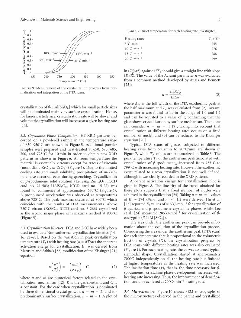
Table 3: Onset temperature for each heating rate investigated.
Heating rates Tp (◦C)
5◦C·min−1 755
10◦C·min−1 776
15◦C·min−1 788
20◦C·min−1 799
ln (T2p/α
n) against 1/Tp should give a straight line with slope(Ec/R). The value of the Avrami parameter n was evaluatedfrom a common method developed by Augis and Bennett[23]:
n = 2.5RT2p
EcΔw, (3)
where Δw is the full width of the DTA exothermic peak atthe half maximum and Ec was calculated from (2). Avramiparameter n was found to be in the range of 1.0 and 1.2and can be adjusted to a value of 1, confirming that theglass shows crystallization by surface mechanism. Then, onecan consider n = m = 1 [9], taking into account thatcrystallization at different heating rates occurs on a fixednumber of nuclei, and (3) can be reduced to the Kissingerequation [20].
Typical DTA scans of glasses subjected to differentheating rates from 5◦C/min to 20◦C/min are shown inFigure 7, while Tp values are summarized in Table 3. Thepeak temperature Tp of the exothermic peak associated withcrystallization of β-spodumeness increased from 755◦C to799◦C with increasing heating rate. However, the exothermicevent related to zircon crystallization is not well defined,although it was clearly recorded in the XRD patterns.
Apparent activation energy for crystallization plot isgiven in Figure 8. The linearity of the curve obtained forthese plots suggests that a fixed number of nuclei wereachieved in the crystallization [24]. Taking n = m = 1 valuesof Ec ∼ 274 kJ/mol and n ∼ 1.2 were derived. Hu et al.[25] reported Ec values of 415 kJ·mol−1 for crystallization ofβ-quartzss and β-spodumene crystalline phases, whilst Leeet al. [24] measured 285 kJ·mol−1 for crystallization of β-eucryptite (β-LiAl [SiO4]).
The area under the exothermic peak can provide infor-mation about the evolution of the crystallization process.Considering the area under the exothermic peak (DTA scan)for each temperature that is proportional to the volumetricfraction of crystals (X), the crystallization progress byDTA scans with different heating rates was also evaluated(Figure 9). For each heating rate, the curves assumed typicalsigmoidal shape. Crystallization started at approximately700◦C independently on all the heating rate but finishedat higher temperatures as the heating rate was increased.The incubation time (τ), that is, the time necessary for β-spodumeness crystalline phase development, increases withheating rate increasing. Thus, the improvement of densifica-tion could be achieved at 20◦C·min−1 heating rate.
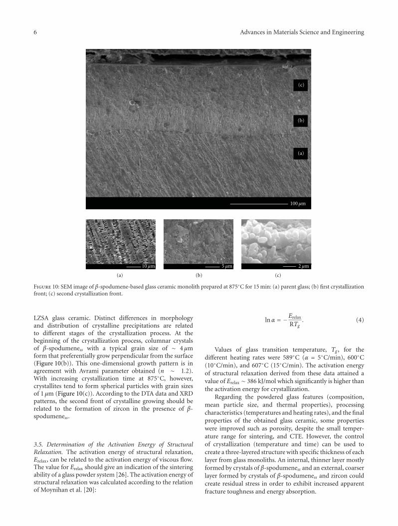
3.4. Microstructure. Figure 10 shows SEM micrographs ofthe microstructures observed in the parent and crystallized
6 Advances in Materials Science and Engineering
(a)
(b)
(c)
(a) (b) (c)
100 μm
5 μm10 μm 2 μm
Figure 10: SEM image of β-spodumene-based glass ceramic monolith prepared at 875◦C for 15 min: (a) parent glass; (b) first crystallizationfront; (c) second crystallization front.
LZSA glass ceramic. Distinct differences in morphologyand distribution of crystalline precipitations are relatedto different stages of the crystallization process. At thebeginning of the crystallization process, columnar crystalsof β-spodumeness with a typical grain size of ∼ 4 μmform that preferentially grow perpendicular from the surface(Figure 10(b)). This one-dimensional growth pattern is inagreement with Avrami parameter obtained (n ∼ 1.2).With increasing crystallization time at 875◦C, however,crystallites tend to form spherical particles with grain sizesof 1 μm (Figure 10(c)). According to the DTA data and XRDpatterns, the second front of crystalline growing should berelated to the formation of zircon in the presence of β-spodumeness.
3.5. Determination of the Activation Energy of StructuralRelaxation. The activation energy of structural relaxation,Erelax, can be related to the activation energy of viscous flow.The value for Erelax should give an indication of the sinteringability of a glass powder system [26]. The activation energy ofstructural relaxation was calculated according to the relationof Moynihan et al. [20]:
lnα = −Erelax
RTg. (4)
Values of glass transition temperature, Tg , for thedifferent heating rates were 589◦C (α = 5◦C/min), 600◦C(10◦C/min), and 607◦C (15◦C/min). The activation energyof structural relaxation derived from these data attained avalue of Erelax ∼ 386 kJ/mol which significantly is higher thanthe activation energy for crystallization.
Regarding the powdered glass features (composition,mean particle size, and thermal properties), processingcharacteristics (temperatures and heating rates), and the finalproperties of the obtained glass ceramic, some propertieswere improved such as porosity, despite the small temper-ature range for sintering, and CTE. However, the controlof crystallization (temperature and time) can be used tocreate a three-layered structure with specific thickness of eachlayer from glass monoliths. An internal, thinner layer mostlyformed by crystals of β-spodumeness and an external, coarserlayer formed by crystals of β-spodumeness and zircon couldcreate residual stress in order to exhibit increased apparentfracture toughness and energy absorption.
Advances in Materials Science and Engineering 7
4. Conclusions
Taking into account some interesting thermal and dielectricproperties, a selected β-spodumene-based glass ceramiccomposition (16.9Li2O·5.0ZrO2·65.1SiO2·8.6Al2O3) wasused for crystallization kinetics investigation by means ofNonisothermal method. The crystallization mechanism wasfound to be predominantly surface crystallization when theparticle size is small. Two crystallization fronts regardingthe crystalline phases formed, β-spodumeness and zircon,were identified starting at approximately 670◦C and 700◦C,respectively. The morphology of the microstructures showeda columnar structure for the former and a globular for thesecond one. Apparent activation energy for crystallization Ecwas found to be in the range 274 kJ/mol with an Avramiparameter n of 1 that is compared very favorably with SEMobservations. At 850◦C/10 min, a low-porosity (3.2%), low-CTE (2.38× 10⁻⁶◦C−1), low-dielectric constant (9.97± 0.84)material was obtained. Moreover, the dielectric loss at 1 MHzwas <0.3%. A value of 386 kJ·mol−1 was obtained for theactivation energy of structural relaxation Erelax, in which itsvalue is significantly higher than the activation energy forcrystallization, hindering densification of material.
Acknowledgments
The authors are grateful to the Brazilian Foundation forthe Coordination of Higher Education Graduate Train-ing (CAPES), to the National Council of Scientific andTechnological Development (CNPq), and to the GermanFoundation for Interchange (DAAD) for supporting thiswork.
References
[1] R. R. Tummala, “Ceramic and glass ceramic packaging in the1990s,” Journal of the American Ceramic Society, vol. 74, pp.895–908, 1991.
[2] Y. Shimada, K. Utsumi, M. Suzuki, H. Takamizawa, M.Nitta, and T. Watari, “Low firing temperature multilayer glassceramic substrate,” IEEE Transactions on Components, Hybrids,and Manufacturing Technology, vol. 6, no. 4, pp. 382–388,1983.
[3] C. R. Chang and J. H. Jean, “Crystallization kinetics and mech-anism of low-dielectric, low-temperature, cofirable CaO-B2O3-SiO2 glass-ceramics,” Journal of the American CeramicSociety, vol. 82, no. 7, pp. 1725–1732, 1999.
[4] O. R. K. Montedo, F. M. Bertan, R. Piccoli, D. Hotza, A.N. Klein, and A. P. N. de Oliveira, “Low thermal expansionsinterered LZSA glass-ceramics,” American Ceramic SocietyBulletin, vol. 87, no. 7, pp. 34–40, 2008.
[5] C. M. Gomes, A. P. N. Oliveira, D. Hotza, N. Travitzky,and P. Greil, “LZSA glass-ceramic laminates: fabricationand mechanical properties,” Journal of Materials ProcessingTechnology, vol. 206, no. 1–3, pp. 194–201, 2008.
[6] O. R. K. Montedo, F. J. Floriano, J. de Oliveira Filho, E.Angoletto, and A. M. Bernardin, “Sintering behavior of LZSAglass-ceramics,” Materials Research, vol. 12, no. 2, pp. 197–200,2009.
[7] C. M. Gomes, C. R. Rambo, A. P. N. de Oliveira et al., “Col-loidal processing of glass-ceramics for laminated object man-ufacturing,” Journal of the American Ceramic Society, vol. 92,no. 6, pp. 1186–1191, 2009.
[8] W. A. Johnson and R. F. Mehl, “Reaction kinetics in processesof nucleation and growth,” AIME Transactions, vol. 135, pp.416–442, 1939.
[9] I. W. Donald and B. L. Metcalfe, “Thermal properties andcrystallization kinetics of a sodium aluminophosphate basedglass,” Journal of Non-Crystalline Solids, vol. 348, pp. 118–122,2004.
[10] A. Marotta, A. Buri, and F. Branda, “Surface and bulk crys-tallization in non-isothermal devitrification of glasses,” Ther-mochimica Acta, vol. 40, pp. 397–403, 1980.
[11] F. Branda, “Nucleation and crystal growth in inorganic glass-forming systems: a DTA study,” Thermochimica Acta, vol. 203,pp. 373–378, 1992.
[12] I. W. Donald, “The crystallization kinetics of a glass based onthe cordierite composition studied by DTA and DSC,” Journalof Materials Science, vol. 30, no. 4, pp. 904–915, 1995.
[13] A. P. N. de Oliveira, A. B. Corradi, L. Barbieri, C. Leonelli,and T. Manfredini, “The effect of the addition of ZrSiO4
on the crystallization of 30Li2O/70SiO2 powdered glass,”Thermochimica Acta, vol. 286, no. 2, pp. 375–386, 1996.
[14] Y. Hu and C. L. Huang, “Crystallization kinetics of theLiNbO3-SiO2-Al2O3 glass,” Journal of Non-Crystalline Solids,vol. 278, no. 1–3, pp. 170–177, 2000.
[15] H. Shao, K. Liang, and F. Peng, “Crystallization kinetics ofMgO-Al2O3-SiO2 glass-ceramics,” Ceramics International, vol.30, no. 6, pp. 927–930, 2004.
[16] E. R. Shaaban, “Non-isothermal crystallization kinetic studieson a ternary, Sb0.14As0.38Se0.48 chalcogenide semi-conductingglass,” Physica B, vol. 373, no. 2, pp. 211–216, 2006.
[17] M. S. Bapna and H. J. Mueller, “Thermodilatometric char-acterization for devitrification of a micaceous dental glass-ceramic,” Journal of the American Ceramic Society, vol. 82, no.7, pp. 1771–1776, 1999.
[18] B. Karmakar, P. Kundu, S. Jana, and R. N. Dwivedi, “Crys-tallization kinetics and mechanism of low-expansion lithiumaluminosilicate glass-ceramics by dilatometry,” Journal of theAmerican Ceramic Society, vol. 85, no. 10, pp. 2572–2574,2002.
[19] R. K. Thakur and S. Thiagarajan, “Studies in catalyzedcrystallization of glasses: a DTA method,” Glass and CeramicBulletin, vol. 13, pp. 33–45, 1966.
[20] C. T. Moynihan, A. J. Easteal, M. A. Debolt, and J. Tucker,“Dependence of the fictive temperature of glass on coolingrate,” Journal of the American Ceramic Society, vol. 59, pp. 12–16, 1976.
[21] H. E. Kissinger, “Variation of peak temperature with heatingrate in differential thermal analysis,” Journal of Research of theNational Bureau of Standards, vol. 57, pp. 217–221, 1956.
[22] T. Ozawa, “Kinetics of non-isothermal crystallization,” Poly-mer, vol. 12, no. 3, pp. 150–158, 1971.
[23] J. A. Augis and J. E. Bennett, “Calculation of the Avramiparameters for heterogeneous solid state reactions using amodification of the Kissinger method,” Journal of ThermalAnalysis, vol. 13, no. 2, pp. 283–292, 1978.
[24] K. Lee, D. A. Hirschfeld, and J. J. Brown, “In situ whisker-reinforced β-eucryptite glass-ceramic: I, morphology andcrystallization kinetics,” Journal of the American CeramicSociety, vol. 79, no. 3, pp. 597–602, 1996.

8 Advances in Materials Science and Engineering
[25] A. M. Hu, M. Li, D. L. M. Dali, and K. M. Liang, “Crystalliza-tion and properties of a spodumene-willemite glass ceramic,”Thermochimica Acta, vol. 437, no. 1-2, pp. 110–113, 2005.
[26] E. M. Rabinovich, “Preparation of glass by sintering,” Journalof Materials Science, vol. 20, no. 12, pp. 4259–4297, 1985.
Hindawi Publishing CorporationAdvances in Materials Science and EngineeringVolume 2011, Article ID 316513, 16 pagesdoi:10.1155/2011/316513
Review Article
Formation and Device Application of Ge NanowireHeterostructures via Rapid Thermal Annealing
Jianshi Tang,1 Chiu-Yen Wang,2 Faxian Xiu,1, 3 Yi Zhou,1 Lih-Juann Chen,2 and Kang L. Wang1
1 Device Research Laboratory, Department of Electrical Engineering, University of California, Los Angeles, CA 90095, USA2 Department of Materials Science and Engineering, National Tsing Hua University, Hsinchu 30013, Taiwan3 Department of Electrical and Computer Engineering, Iowa State University, Ames, IA 50014, USA
Correspondence should be addressed to Kang L. Wang, [email protected]
Received 21 April 2011; Accepted 14 June 2011
Academic Editor: Joseph Lai
Copyright © 2011 Jianshi Tang et al. This is an open access article distributed under the Creative Commons Attribution License,which permits unrestricted use, distribution, and reproduction in any medium, provided the original work is properly cited.
We reviewed the formation of Ge nanowire heterostructure and its field-effect characteristics by a controlled reaction between asingle-crystalline Ge nanowire and Ni contact pads using a facile rapid thermal annealing process. Scanning electron microscopyand transmission electron microscopy demonstrated a wide temperature range of 400∼500◦C to convert the Ge nanowire toa single-crystalline Ni2Ge/Ge/Ni2Ge nanowire heterostructure with atomically sharp interfaces. More importantly, we studiedthe effect of oxide confinement during the formation of nickel germanides in a Ge nanowire. In contrast to the formationof Ni2Ge/Ge/Ni2Ge nanowire heterostructures, a segment of high-quality epitaxial NiGe was formed between Ni2Ge with theconfinement of Al2O3 during annealing. A twisted epitaxial growth mode was observed in both two Ge nanowire heterostructuresto accommodate the large lattice mismatch in the NixGe/Ge interface. Moreover, we have demonstrated field-effect transistorsusing the nickel germanide regions as source/drain contacts to the Ge nanowire channel. Our Ge nanowire transistors have showna high-performance p-type behavior with a high on/off ratio of 105 and a field-effect hole mobility of 210 cm2/Vs, which showeda significant improvement compared with that from unreacted Ge nanowire transistors.
1. Introduction
As an important one-dimensional material, semiconductornanowire has attracted enormous research interest for itsunique electrical properties, which has promising applica-tions as building blocks for nanoelectronics [1–5]. Since2004, there have been a lot of efforts on studying the thermaldiffusion of metal into a single-crystalline Si nanowire, inwhich a silicide/silicon/silicide nanowire heterostructure isformed by solid-state reactions between the Si nanowire andmetal contacts. Many metals (contact pads or nanowires)have been studied as the diffusion source, such as Ni [6–8],Co [9], Pt [10], and Mn [11]. One of the salient featuresin this nanowire heterostructure is the atomically sharp in-terface between the Si nanowire and the formed silicide na-nowire. Such clean interface may help to avoid Fermi-levelpinning effect, which is commonly observed in conventionalmetal-semiconductor contacts [12]. Also, the nanowire
heterostructure can be easily used to fabricate nanowire field-effect transistors (FETs) using the formed silicide regionsas the source/drain contacts to the Si nanowire channel[6, 7, 10]. The channel length can be well controlled by theannealing time and growth length of silicide, therefore, canbe aggressively shrunk down to sub-50 nm [11]. Clearly, thisprocess offers great advantages over modern high-cost andcomplex photolithography technology to fabricate short-channel transistors and may further facilitate the advance ofscaled nanodevices.
Compared with Si nanowire, metal-Ge nanowire is a newsystem of interest, since Ge is an important complementto Si with even higher carrier mobilities for further deviceminiaturization compatible to the existing CMOS technol-ogy [1, 2]. For Ge, the atomically sharp interface is ofparticular interest to alleviate the Fermi-level pinning effectin the metal-Ge contact, since Ge has a high density of in-terface states due to native defects on the Ge surface [12].
2 Advances in Materials Science and Engineering
Experimentally, Yamane et al. have demonstrated the epitax-ial growth of high-quality Fe3Si on Ge(111) substrate with anatomically controlled interface, which successfully depinedthe Fermi-level of Fe3Si/Ge contact [19]. It is, therefore,highly desirable to achieve a metallic contact to Ge with ahigh-quality interface. On the other hand, many germanides,such as Mn5Ge3 and Ni3Ge, exhibit ferromagnetism aboveroom temperature [20, 21], and thus offer great advantagesover silicides for future applications in spintronics, such asrealizing spin injection into semiconductor from a ferro-magnetic contact. Therefore, there is an increasing researchinterest on the metal-Ge nanowire system, such as Ni-Ge[13–15] and Cu-Ge [16–18]. For comparison, Table 1 brieflysummarizes the literature report of Si and Ge nanowireheterostructures formed by solid-state reactions between asemiconductor nanowire and metal contacts. It is noted thatthe annealing temperature of metal-Ge nanowire system isusually lower than that of metal-Si nanowire system, whichis partially due to a lower melting point of Ge than Si. Thelow-temperature process in metal-Ge nanowire systems isfavorable to reduce the thermal budget in forming nanowireheterostructures toward future process integration.
In this paper, we will first discuss the formation of single-crystalline Ge nanowire heterostructure by the solid-statereaction between a Ge nanowire and Ni contact pads. By acomparative study of with or without an Al2O3 capping layerduring annealing, we study the effect of oxide confinementin the growth of germanide in a Ge nanowire. A detailedtransmission electron microscopy (TEM) analysis includingthe epitaxial relationships is presented in this section. Inthe second part of this paper, we will introduce electricalcharacterizations of Ge nanowire back-gate FETs fabricatedusing the Ge nanowire heterostructures. Specifically, theeffect of Al2O3 capping layer on the device performance isstudied in this section. Finally, we will discuss the possibleresearch directions for future work on the Ge nanowire het-erostructures, especially for promising applications in spin-tronics and further study on the growth dynamics.
2. Experimental Results
The growth of Ge nanowires can be accomplished by avariety of techniques. In this study, two popular methodswere employed to synthesize single-crystalline Ge nanowirewith 〈111〉 growth direction. One is the supercritical fluid-liquid-solid (SFLS) approach, in which Ge nanowires wereproduced in highly pressurized supercritical fluids enrichedwith organogermane precursors and metal nanocrystals ascatalyst [22, 23]. The typical diameter of as-synthesized Genanowires is around 40–50 nm and the length could be morethan 10 μm. The other approach is the vapor-liquid-solid(VLS) method, in which metal (such as Au) catalyzed Genanowires were grown on SiO2/Si(100) substrates by meansof chemical vapor deposition (CVD) using a gaseous Geprecursor GeH4 [24]. The VLS-grown Ge nanowires aretypically 70–80 nm in diameter and have lengths over 10 μm.The reported carrier mobility of VLS-grown Ge nanowires ishigher than SFLS-synthesized Ge nanowires [13, 14], while
the latter method is claimed to provide a better control ofthe nanowire size and a higher product yield [23, 25]. Inboth two methods, Ge nanowires are not doped on purposeduring growth, but unintentional doping usually occurs [26,27].
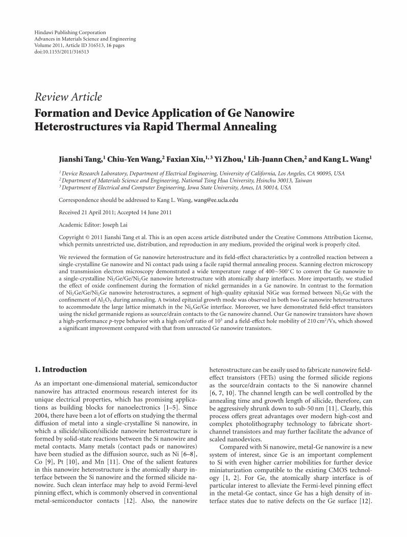
To form NixGe/Ge nanowire heterostructures, SFLS-synthesized Ge nanowires diluted in isopropyl alcohol (IPA)were dispersed onto a SiO2/Si substrate. The top thermalSiO2 was about 330 nm thick. The Si substrate was degen-erately doped with a resistivity of 1–5 ×10⁻³ Ω-cm, whichserved as a back gate for further device characterization. E-beam lithography (EBL) was used to define Ni contacts toGe nanowires. Before e-beam evaporation of about 120 nm-thick Ni (with the purity of 99.995% and in vacuum ata pressure lower than 10−6 Torr), the sample was dippedinto diluted hydrofluoric acid (HF) for 15 s to completelyremove native oxide in the contact region. A field-emissionscanning electron microscopy (JEOL JSM-6700 FESEM) wasused to examine the sample morphology before and afterthe annealing process. Figures 1(a) and 1(b) show the deviceschematics before and after the thermal diffusion of Niinto the Ge nanowire. Figure 1(c) shows the SEM imageof the as-fabricated Ge nanowire device showing a uni-form contrast. Then the sample was annealed with rapidthermal annealing (RTA) in the ambient of N2 to allowNi thermal intrusion into Ge nanowire and subsequentlyform NixGe/Ge heterostructures along the nanowire. Inthe previous study on the interfacial reactions of Ni thinfilm on Ge(111) substrate, the germanide phase formationsequence was found to be Ni2Ge and NiGe at increasingtemperatures in the range of 160◦C to 600◦C [28]. Variousannealing temperatures ranging from 400◦C to 700◦C wereused in this study to optimize the formation of nanowireheterostructures. It is found out that Ge nanowires wereeasily broken at a high annealing temperature (>550◦C) dueto the significant reduction of the melting point for Genanowires compared with that of bulk Ge [29]. When thetemperature decreased to 400◦C–500◦C, clear diffusion of Niinto the Ge nanowire was also observed and the formed ger-manide was identified to be Ni2Ge (refer to the TEM analysislater). Figure 1(d) shows the SEM image of the Ge nanowiredevice upon RTA at 500◦C for 60 s, in which clear contrastwas observed between the Ge nanowire and the formednickel germanide nanowire due to the conductivity dif-ference. The remained Ge region was easily controlled downto 650 nm, and it can be further reduced to sub-100 nm[11, 16]. Similar contrast was also observed after RTA at400◦C for 40 s, as shown in Figure 1(e).
In order to identify the phase of the formed germanideand the epitaxial relationship of germanide-germanium in-terface, in situ TEM was used to study the formation processand reaction kinetics. To prepare the TEM sample, thesingle-crystalline Ge nanowires were dispersed on the TEMgrid with a square opening of a Si3N4 thin film. The low-stress Si3N4 film was deposited by low-pressure chemicalvapor deposition (LPCVD). The Si3N4 film was about 50 nmthick, which provided a reliable mechanical support forGe nanowire devices during the fabrication process and atthe same time to assure it is transparent to the electron
Advances in Materials Science and Engineering 3
Table 1: Summary of Si and Ge nanowire heterostructures formed by solid-state reactions between a semiconductor nanowire and metalcontacts.
Material system Annealing condition (◦C) Formed silicide/germanide Metal diffusion source
Ni-Si [6] 550 NiSi Ni contact pad
Ni-Si [7] 470 NiSix (not identified) Ni contact pad
Ni-Si [8] 500–700 NiSi Ni nanowire
Co-Si [9]700 CoSi Co nanodots
800 Co2Si Co nanodots
Pt-Si [10] 520 PtSi Pt contact pad
Mn-Si [11] 650 MnSi Mn contact pad
Ni-Ge [13] 400–500 Ni2Ge Ni contact pad
Ni-Ge [14] 450 (capped with Al2O3) Ni2Ge/NiGe Ni contact pad
Ni-Ge [15] 300–450 Ni2Ge Ni contact pad
Cu-Ge [16–18] 310 Cu3Ge Cu contact pad
Ge
Ni
SiO2
Si
(a)
Ge
Ni
SiO2
Si
NixGe
(b)
0.5 μm
(c)
1 μm
(d)
0.5 μm
(e)
Figure 1: Formation of Ni2Ge/Ge/Ni2Ge heterostructures. Schematic illustration showing (a) before and (b) after the diffusion process of Niinto the Ge nanowire forming a Ni2Ge/Ge/Ni2Ge heterostructure. (c) SEM image of the Ge nanowire device with EBL defined Ni electrodes.(d) SEM image of the Ni2Ge/Ge/Ni2Ge heterostructure after RTA at 500◦C for 60 s in which the length of the Ge region was easily controlledto submicron range. The arrows indicate the growth tips of the Ni2Ge nanowire. (e) SEM image of the Ni2Ge/Ge/Ni2Ge heterostructure afterRTA at 400◦C for 40 s. The arrows indicate the growth tips of the Ni2Ge nanowire. Reproduced from [13].
beam without interference with images of the nanowires.EBL-defined Ni pads were employed as the Ni diffusionsource. A JEOL-2010 TEM (operated at 200 KV with a point-to-point resolution of 0.25 nm) attached with an energydispersive spectrometer (EDS) was used to investigate themicrostructures and to determine the compositions of thesamples. To in situ observe the reactions of the Ni electrodeswith Ge nanowires, the samples were heated inside TEMwith a heating holder (Gatan 652 double tilt heating holderconnected with a power supply to heat up the samples tothe desired temperature) under a RTA mode with a pressure
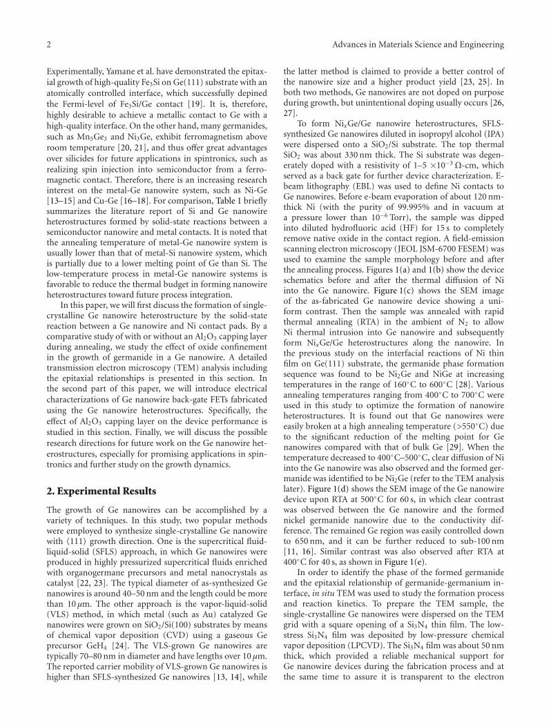
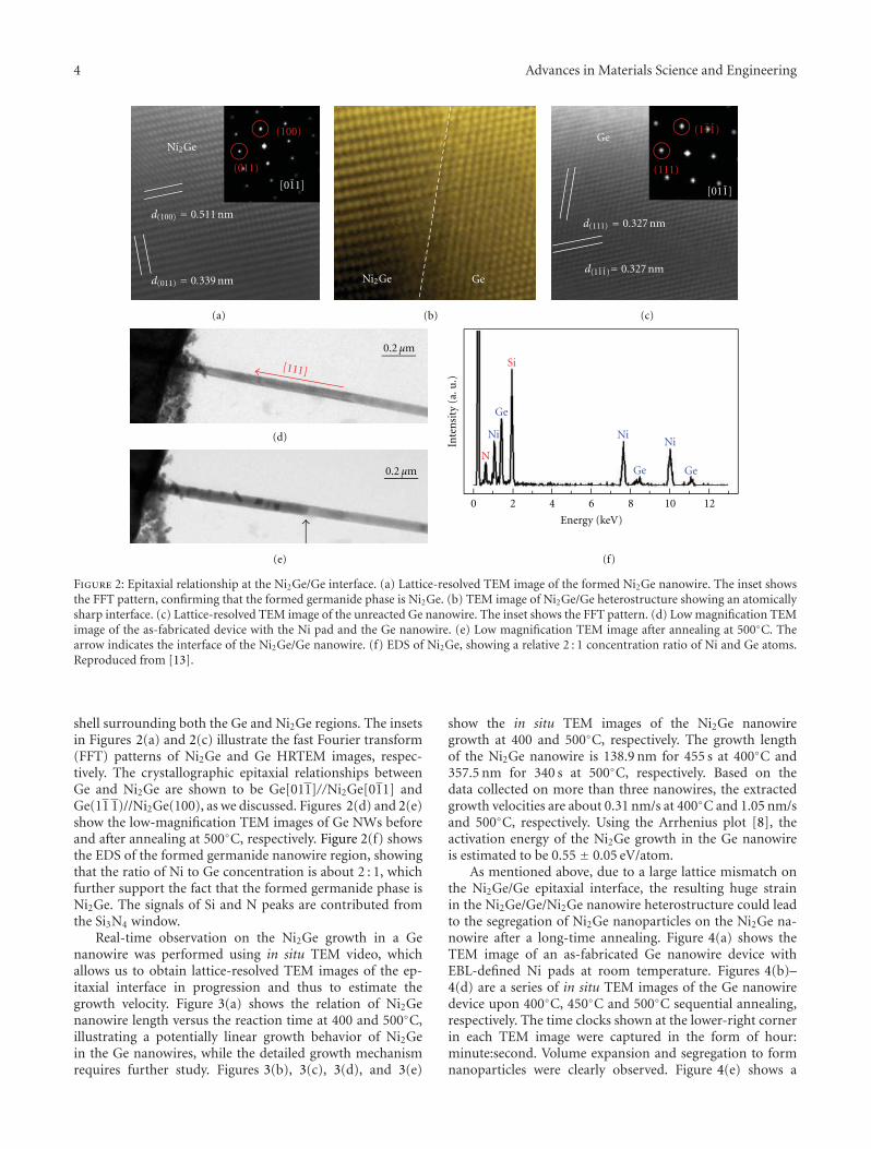
below 10−6 Torr. Figures 2(a)–2(c) show high-resolutionTEM (HRTEM) images of the formed NixGe/Ge interfaceupon 500◦C annealing. According to the lattice-resolvedHRTEM analysis, the formed germanide was identified tobe single-crystalline Ni2Ge with an orthorhombic latticestructure and lattice constants a = 0.511 nm, b = 0.383 nm,and c = 0.726 nm (space group 62). It was observed thata large lattice mismatch of 56.3% at the Ni2Ge/Ge epitaxialinterface could result in the segregation of nanoparticles (seeFigure 4). In Figure 2(b), a clean and sharp interface betweenNi2Ge/Ge was observed with an approximately 1 nm GeOx
4 Advances in Materials Science and Engineering
Ni2Ge
Ge
Ge GeN
Ni NiNi
Si
0 2 4 6 8 10 12
Energy (keV)
Inte
nsi
ty(a
.u.)
d(111) = 0.327 nm
d(011) = 0.339 nm
d(100) = 0.511 nm
)d(111 = 0.327 nm
(111)
(111)
(011)
[011] [011]
(100)
Ni2Ge
Ge
Ge
0.2 μm
0.2 μm
[111]
(a) (b) (c)
(d)
(e) (f)
Figure 2: Epitaxial relationship at the Ni2Ge/Ge interface. (a) Lattice-resolved TEM image of the formed Ni2Ge nanowire. The inset showsthe FFT pattern, confirming that the formed germanide phase is Ni2Ge. (b) TEM image of Ni2Ge/Ge heterostructure showing an atomicallysharp interface. (c) Lattice-resolved TEM image of the unreacted Ge nanowire. The inset shows the FFT pattern. (d) Low magnification TEMimage of the as-fabricated device with the Ni pad and the Ge nanowire. (e) Low magnification TEM image after annealing at 500◦C. Thearrow indicates the interface of the Ni2Ge/Ge nanowire. (f) EDS of Ni2Ge, showing a relative 2 : 1 concentration ratio of Ni and Ge atoms.Reproduced from [13].
shell surrounding both the Ge and Ni2Ge regions. The insetsin Figures 2(a) and 2(c) illustrate the fast Fourier transform(FFT) patterns of Ni2Ge and Ge HRTEM images, respec-tively. The crystallographic epitaxial relationships betweenGe and Ni2Ge are shown to be Ge[011]//Ni2Ge[011] andGe(11 1)//Ni2Ge(100), as we discussed. Figures 2(d) and 2(e)show the low-magnification TEM images of Ge NWs beforeand after annealing at 500◦C, respectively. Figure 2(f) showsthe EDS of the formed germanide nanowire region, showingthat the ratio of Ni to Ge concentration is about 2 : 1, whichfurther support the fact that the formed germanide phase isNi2Ge. The signals of Si and N peaks are contributed fromthe Si3N4 window.
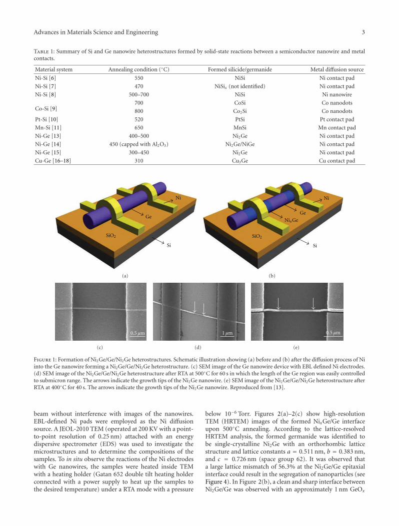
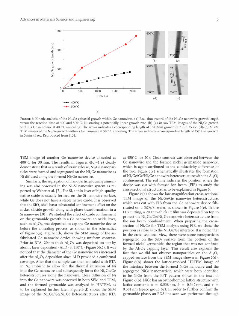
Real-time observation on the Ni2Ge growth in a Genanowire was performed using in situ TEM video, whichallows us to obtain lattice-resolved TEM images of the ep-itaxial interface in progression and thus to estimate thegrowth velocity. Figure 3(a) shows the relation of Ni2Genanowire length versus the reaction time at 400 and 500◦C,illustrating a potentially linear growth behavior of Ni2Gein the Ge nanowires, while the detailed growth mechanismrequires further study. Figures 3(b), 3(c), 3(d), and 3(e)
show the in situ TEM images of the Ni2Ge nanowiregrowth at 400 and 500◦C, respectively. The growth lengthof the Ni2Ge nanowire is 138.9 nm for 455 s at 400◦C and357.5 nm for 340 s at 500◦C, respectively. Based on thedata collected on more than three nanowires, the extractedgrowth velocities are about 0.31 nm/s at 400◦C and 1.05 nm/sand 500◦C, respectively. Using the Arrhenius plot [8], theactivation energy of the Ni2Ge growth in the Ge nanowireis estimated to be 0.55 ± 0.05 eV/atom.
As mentioned above, due to a large lattice mismatch onthe Ni2Ge/Ge epitaxial interface, the resulting huge strainin the Ni2Ge/Ge/Ni2Ge nanowire heterostructure could leadto the segregation of Ni2Ge nanoparticles on the Ni2Ge na-nowire after a long-time annealing. Figure 4(a) shows theTEM image of an as-fabricated Ge nanowire device withEBL-defined Ni pads at room temperature. Figures 4(b)–4(d) are a series of in situ TEM images of the Ge nanowiredevice upon 400◦C, 450◦C and 500◦C sequential annealing,respectively. The time clocks shown at the lower-right cornerin each TEM image were captured in the form of hour:minute:second. Volume expansion and segregation to formnanoparticles were clearly observed. Figure 4(e) shows a
Advances in Materials Science and Engineering 5
0′00′′
0′00′′
7′35′′
5′40′′0 500 1000 1500 20000
500
1000
1500
Time (s)
Ni 2
Ge
grow
thle
ngt
h(n
m)
400◦C
400◦C
500◦C
500◦C
139n
m
357.5n
m
(a)
(b) (c)
(d) (e)
Figure 3: Kinetic analysis of the Ni2Ge epitaxial growth within Ge nanowires. (a) Real-time record of the Ni2Ge nanowire growth lengthversus the reaction time at 400 and 500◦C, illustrating a potentially linear growth rate. (b)-(c) In situ TEM images of the Ni2Ge growthwithin a Ge nanowire at 400◦C annealing. The arrow indicates a corresponding length of 138.9 nm growth in 7 min 35 sec. (d)-(e) In situTEM images of the Ni2Ge growth within a Ge nanowire at 500◦C annealing. The arrow indicates a corresponding length of 357.5 nm growthin 5 min 40 sec. Reproduced from [13].
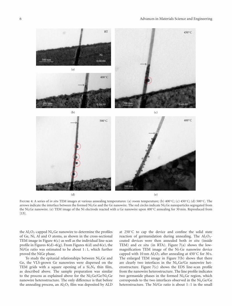
TEM image of another Ge nanowire device annealed at400◦C for 30 min. The results in Figures 4(c)–4(e) clearlydemonstrate that as a result of strain release, Ni2Ge nanopar-ticles were formed and segregated on the Ni2Ge nanowire asNi diffused along the formed Ni2Ge nanowire.
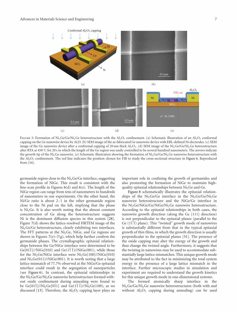
Similarly, the segregation of nanoparticles during anneal-ing was also observed in the Ni-Si nanowire system as re-ported by Weber et al. [7]. For Si, a thin layer of high-qualitynative oxide is usually formed on the Si nanowire surface,while Ge does not have a stable native oxide. It is observedthat the SiO2 shell has a substantial confinement effect on thenickel silicide growth along with phase transformation in aSi nanowire [30]. We studied the effect of oxide confinementon the germanide growth in a Ge nanowire; an oxide layer,such as Al2O3, was deposited to cap the Ge nanowire devicebefore the annealing process, as shown in the schematicsof Figure 5(a). Figure 5(b) shows the SEM image of the as-fabricated Ge nanowire device showing uniform contrast.Prior to RTA, 20 nm thick Al2O3 was deposited on top byatomic layer deposition (ALD) at 250◦C (Figure 5(c)). It wasnoticed that the diameter of the Ge nanowire was increasedafter the Al2O3 deposition since ALD provided a conformalcoverage. After that the sample was then annealed with RTAin N2 ambient to allow for the thermal intrusion of Niinto the Ge nanowire and subsequently form the NixGe/Geheterostructures along the nanowire. Clear diffusion of Niinto the Ge nanowire was observed in both SEM and TEM,and the formed germanide was analyzed in HRTEM, asto be explained further later. Figure 5(d) shows the SEMimage of the NixGe/Ge/NixGe heterostructures after RTA
at 450◦C for 20 s. Clear contrast was observed between theGe nanowire and the formed nickel germanide nanowire,which is again attributed to the conductivity difference ofthe two. Figure 5(e) schematically illustrates the formationof NixGe/Ge/NixGe nanowire heterostructure with the Al2O3
confinement. The red line indicates the position where thedevice was cut with focused ion beam (FIB) to study thecross-sectional structure, as to be explained in Figure 6.
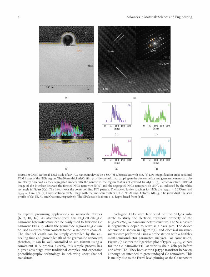
Figure 6(a) shows the low-magnification cross-sectionalTEM image of the NixGe/Ge nanowire heterostructure,which was cut with FIB from the Ge nanowire device fab-ricated on a SiO2/Si wafer, as shown in Figure 5(e). BeforeFIB cutting, a 200 nm-thick Pt film was deposited on top toprotect the NixGe/Ge/NixGe nanowire heterostructure fromthe ion beam bombardment. When preparing the cross-section of NixGe for TEM analysis using FIB, we chose theposition as close as to the NixGe/Ge interface. It is noted thatin the cross-sectional view, there were some nanoparticlessegregated on the SiO2 surface from the bottom of theformed nickel germanide, the region that was not confinedby the Al2O3 capping layer. This result also explains thefact that we did not observe nanoparticles on the Al2O3
capped surface from the SEM image shown in Figure 5(d).Figure 6(b) shows the lattice-resolved HRTEM image ofthe interface between the formed NiGe nanowire and thesegregated NiGe nanoparticle, which were both identifiedto be NiGe from the FFT pattern shown in the inset ofFigure 6(b). NiGe has an orthorhombic lattice structure withlattice constants a = 0.538 nm, b = 0.342 nm, and c =0.581 nm (space group 62). In order to further confirm thegermanide phase, an EDS line scan was performed through
6 Advances in Materials Science and Engineering
Ni
500 nm
200 nm
200 nm200 nm
200 nm
RT
400◦C
400◦C
450◦C
500◦C
0:16:39 0:48:09
1:37:30
0:00:00
(a)
(b) (c)
(d) (e)
Figure 4: A series of in situ TEM images at various annealing temperatures: (a) room temperature; (b) 400◦C; (c) 450◦C; (d) 500◦C. Thearrows indicate the interface between the formed Ni2Ge and the Ge nanowire. The red circles indicate Ni2Ge nanoparticles segregated fromthe Ni2Ge nanowire. (e) TEM image of the Ni electrode reacted with a Ge nanowire upon 400◦C annealing for 30 min. Reproduced from[13].
the Al2O3-capped NixGe nanowire to determine the profilesof Ge, Ni, Al and O atoms, as shown in the cross-sectionalTEM image in Figure 6(c) as well as the individual line-scanprofile in Figures 6(d)–6(g). From Figures 6(d) and 6(e), theNi/Ge ratio was estimated to be about 1 : 1, which furtherproved the NiGe phase.
To study the epitaxial relationships between NixGe andGe, the VLS-grown Ge nanowires were dispersed on theTEM grids with a square opening of a Si3N4 thin film,as described above. The sample preparation was similarto the process as explained above for the Ni2Ge/Ge/Ni2Genanowire heterostructure. The only difference is that beforethe annealing process, an Al2O3 film was deposited by ALD
at 250◦C to cap the device and confine the solid statereaction of germanidation during annealing. The Al2O3-coated devices were then annealed both in situ (insideTEM) and ex situ (in RTA). Figure 7(a) shows the low-magnification TEM image of the Ni-Ge nanowire devicecapped with 10 nm Al2O3 after annealing at 450◦C for 30 s.The enlarged TEM image in Figure 7(b) shows that thereare clearly two interfaces in the NixGe/Ge nanowire het-erostructure. Figure 7(c) shows the EDS line-scan profilefrom the nanowire heterostructure. The line profile indicatestwo germanide phases in the formed NixGe region, whichcorresponds to the two interfaces observed in the NixGe/Geheterostructure. The Ni/Ge ratio is about 1 : 1 in the small
Advances in Materials Science and Engineering 7
Ge
Ni
SiO2
Si
Conformal Al2O3 capping
(a)
0.5 μm
(b)
0.5 μm
(c)
0.5 μm
(d)
GeNi Ni
SiO2
n+-Si (100)
Al2O3
NixGe NixGe
FIB cut
(e)
Figure 5: Formation of NixGe/Ge/NixGe heterostructure with the Al2O3 confinement. (a) Schematic illustration of an Al2O3 conformalcapping on the Ge nanowire device by ALD. (b) SEM image of the as-fabricated Ge nanowire device with EBL-defined Ni electrodes. (c) SEMimage of the Ge nanowire device after a conformal capping of 20 nm thick Al2O3. (d) SEM image of the NixGe/Ge/NixGe heterostructureafter RTA at 450◦C for 20 s in which the length of the Ge region was easily controlled to be several hundred nanometers. The arrows indicatethe growth tip of the NixGe nanowire. (e) Schematic illustration showing the formation of NixGe/Ge/NixGe nanowire heterostructure withthe Al2O3 confinement. The red line indicates the position chosen for FIB to study the cross-sectional structure in Figure 6. Reproducedfrom [14].
germanide region close to the NixGe/Ge interface, suggestingthe formation of NiGe. This result is consistent with theline-scan profile in Figures 6(d) and 6(e). The length of theNiGe region can range from tens of nanometers to hundredsof nanometers in our experiments. On the other hand, theNi/Ge ratio is about 2 : 1 in the other germanide regionclose to the Ni pad on the left, implying that the phaseis Ni2Ge. It is also worth noting that the almost constantconcentration of Ge along the heterostructure suggestsNi is the dominant diffusion species in this system [28].Figure 7(d) shows the lattice-resolved HRTEM image of theNixGe/Ge heterostructure, clearly exhibiting two interfaces.The FFT patterns at the Ni2Ge, NiGe, and Ge regions areshown in Figures 7(e)–7(g), which help further confirm thegermanide phases. The crystallographic epitaxial relation-ships between the Ge/NiGe interface were determined to beGe[011]//NiGe[010] and Ge(11 1)//NiGe(001), while thosefor the Ni2Ge/NiGe interface were Ni2Ge[100]//NiGe[010]and Ni2Ge(011)//NiGe(001). It is worth noting that a largelattice mismatch of 77.7% observed at the NiGe/Ge epitaxialinterface could result in the segregation of nanoparticles(see Figure 6). In contrast, the epitaxial relationships inthe Ni2Ge/Ge/Ni2Ge nanowire heterostructure formed with-out oxide confinement during annealing were found tobe Ge[011]//Ni2Ge[011] and Ge(11 1)//Ni2Ge(100), as wediscussed [13]. Therefore, the Al2O3 capping layer plays an
important role in confining the growth of germanides andalso promoting the formation of NiGe to maintain high-quality epitaxial relationships between Ni2Ge and Ge.
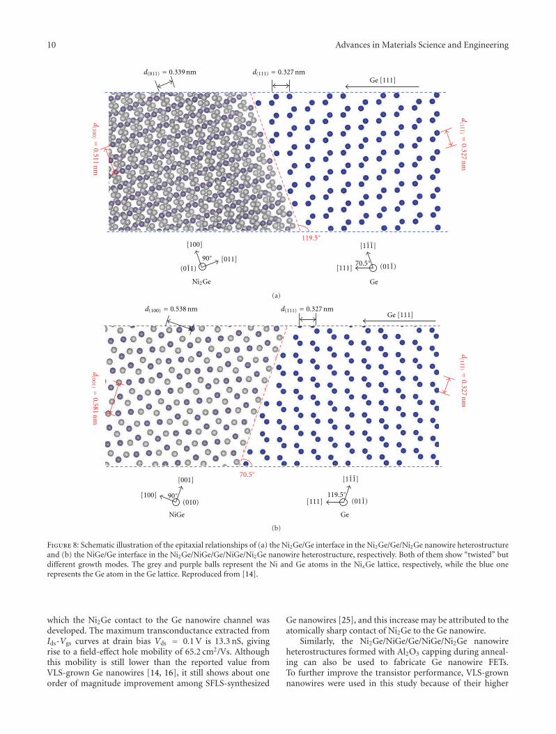
Figure 8 schematically illustrates the epitaxial relation-ships of the Ni2Ge/Ge interface in the Ni2Ge/Ge/Ni2Genanowire heterostructure and the NiGe/Ge interface inthe Ni2Ge/NiGe/Ge/NiGe/Ni2Ge nanowire heterostructure.According to the epitaxial relationships in both cases, thenanowire growth direction (along the Ge [111] direction)is not perpendicular to the epitaxial planes (parallel to theGe (11 1) plane). This “twisted” growth mode of nanowiresis substantially different from that in the typical epitaxialgrowth of thin films, in which the growth direction is usuallyperpendicular to the epitaxial planes [31]. The presence ofthe oxide capping may alter the energy of the growth andthus change the twisted angle. Furthermore, it suggests thatthe twisting in nanowires may be used to accommodate sub-stantially large lattice mismatches. This unique growth modemay be attributed to the fact in minimizing the total systemenergy in the presence of a large lattice mismatch in theinterface. Further microscopic studies in simulation andexperiment are required to understand the growth kineticsfor this unique growth mode in one-dimensional systems.
The formed atomically sharp interface in theNixGe/Ge/NixGe nanowire heterostructures (both with andwithout Al2O3 capping during annealing) can be used
8 Advances in Materials Science and Engineering
[011]
(200)
(011)
100 nmSi
SiO2
SiO2
Pt
Al2O3
Al2O3
0 50 100 150 200
Ge
Ni O
Al
NiGe NP1 nm
NiGe NW
(a) (b)
(c)
(d)
(e)
(f)
(g)
0 50 100 150 200(nm)
0 50 100 150 200(nm)
0 50 100 150 200(nm)
0 50 100 150 200(nm)
(nm)
d(011)
d(200)
Figure 6: Cross-sectional TEM study of a Ni-Ge nanowire device on a SiO2/Si substrate cut with FIB. (a) Low-magnification cross-sectionalTEM image of the NiGe region. The 20 nm thick Al2O3 film provides a conformal capping on the device surface and germanide nanoparticlesare clearly observed as they segregated underneath the nanowire, the region that is not covered by Al2O3. (b) Lattice-resolved HRTEMimage of the interface between the formed NiGe nanowire (NW) and the segregated NiGe nanoparticle (NP), as indicated by the whiterectangle in Figure 5(a). The inset shows the corresponding FFT pattern. The labeled lattice spacings for NiGe are: d(01-1) = 0.295 nm andd(200) = 0.269 nm. (c) Cross-sectional TEM image with the line-scan profiles of Ge, Ni, Al and O atoms. (d)–(g) The individual line-scanprofile of Ge, Ni, Al, and O atoms, respectively, The Ni/Ge ratio is about 1 : 1. Reproduced from [14].
to explore promising applications in nanoscale devices[6, 7, 10, 16]. As aforementioned, this NixGe/Ge/NixGenanowire heterostructure can be easily used to fabricate Genanowire FETs, in which the germanide regions NixGe canbe used as source/drain contacts to the Ge nanowire channel.The channel length can be simply controlled by the an-nealing time and growth length of the germanide nanowire;therefore, it can be well controlled to sub-100 nm using aconvenient RTA process. Clearly, this simple process hasa great advantage over traditional complex and expensivephotolithography technology in achieving short-channeltransistors.
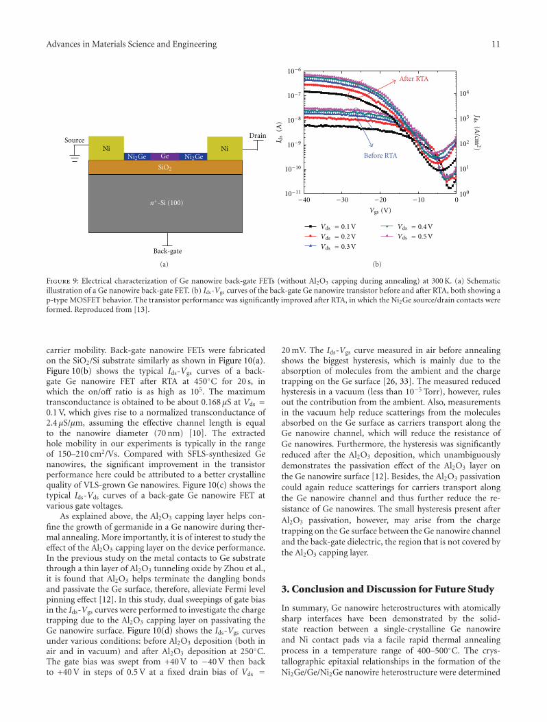
Back-gate FETs were fabricated on the SiO2/Si sub-strate to study the electrical transport property of theNi2Ge/Ge/Ni2Ge nanowire heterostructure. The Si substrateis degenerately doped to serve as a back gate. The deviceschematic is shown in Figure 9(a), and electrical measure-ments were performed using a probe station with a Keithley4200 semiconductor parameter analyzer. For comparison,Figure 9(b) shows the logarithm plot of typical Ids-Vgs curvesfor the Ge nanowire FET at various drain voltages beforeand after RTA. They both show a p-type transistor behavior,although we intended to grow undoped Ge nanowires. Thisis mainly due to the Fermi level pinning at the Ge nanowire
Advances in Materials Science and Engineering 9
Ge
Ge
Ni0
10
20
30
40
Inte
nsi
ty
0 100 200 300 400
Ge
Ge
NiGe
NiGe
NiGe
Ni2Ge
Ni2Ge
Ni2Ge
200 nm
100 nm
(111)
[011]
(111)
[010]
(100)
(001)
[100]
(010)
(001)(011)
5 nm
(nm)
(a)
(b)
(c)
(d)
(e) (f) (g)
d(001)
d(001)
d(100)d(111)
d(111)
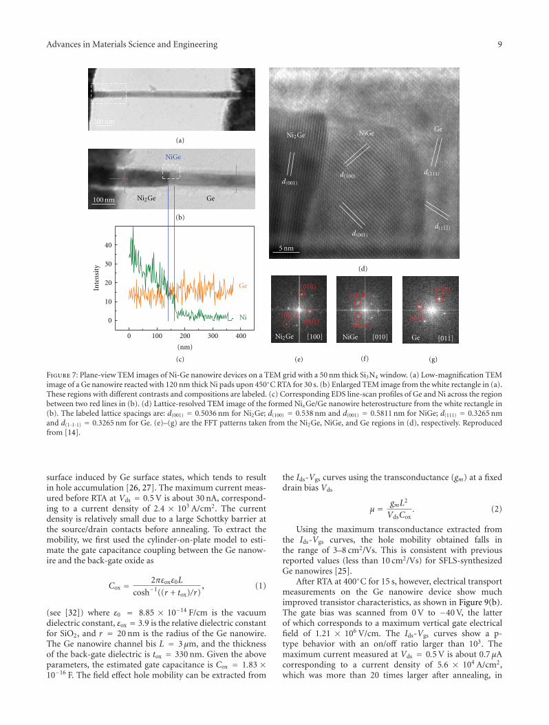
Figure 7: Plane-view TEM images of Ni-Ge nanowire devices on a TEM grid with a 50 nm thick Si3N4 window. (a) Low-magnification TEMimage of a Ge nanowire reacted with 120 nm thick Ni pads upon 450◦C RTA for 30 s. (b) Enlarged TEM image from the white rectangle in (a).These regions with different contrasts and compositions are labeled. (c) Corresponding EDS line-scan profiles of Ge and Ni across the regionbetween two red lines in (b). (d) Lattice-resolved TEM image of the formed NixGe/Ge nanowire heterostructure from the white rectangle in(b). The labeled lattice spacings are: d(001) = 0.5036 nm for Ni2Ge; d(100) = 0.538 nm and d(001) = 0.5811 nm for NiGe; d(111) = 0.3265 nmand d(1-1-1) = 0.3265 nm for Ge. (e)–(g) are the FFT patterns taken from the Ni2Ge, NiGe, and Ge regions in (d), respectively. Reproducedfrom [14].
surface induced by Ge surface states, which tends to resultin hole accumulation [26, 27]. The maximum current meas-ured before RTA at Vds = 0.5 V is about 30 nA, correspond-ing to a current density of 2.4 × 10³ A/cm2. The currentdensity is relatively small due to a large Schottky barrier atthe source/drain contacts before annealing. To extract themobility, we first used the cylinder-on-plate model to esti-mate the gate capacitance coupling between the Ge nanow-ire and the back-gate oxide as
Cox = 2πεoxε0L
cosh−1((r + tox)/r), (1)
(see [32]) where ε0 = 8.85 × 10⁻¹⁴ F/cm is the vacuumdielectric constant, εox = 3.9 is the relative dielectric constantfor SiO2, and r = 20 nm is the radius of the Ge nanowire.The Ge nanowire channel bis L = 3μm, and the thicknessof the back-gate dielectric is tox = 330 nm. Given the aboveparameters, the estimated gate capacitance is Cox = 1.83 ×10⁻¹⁶ F. The field effect hole mobility can be extracted from
the Ids-Vgs curves using the transconductance (gm) at a fixeddrain bias Vds
μ = gmL2
VdsCox. (2)
Using the maximum transconductance extracted fromthe Ids-Vgs curves, the hole mobility obtained falls inthe range of 3–8 cm2/Vs. This is consistent with previousreported values (less than 10 cm2/Vs) for SFLS-synthesizedGe nanowires [25].
After RTA at 400◦C for 15 s, however, electrical transportmeasurements on the Ge nanowire device show muchimproved transistor characteristics, as shown in Figure 9(b).The gate bias was scanned from 0 V to −40 V, the latterof which corresponds to a maximum vertical gate electricalfield of 1.21 × 10⁶ V/cm. The Ids-Vgs curves show a p-type behavior with an on/off ratio larger than 103. Themaximum current measured at Vds = 0.5 V is about 0.7 μAcorresponding to a current density of 5.6 × 10⁴ A/cm2,which was more than 20 times larger after annealing, in
10 Advances in Materials Science and Engineering
Ge [111]d(111) = 0.327 nm
119.5◦
90◦70.5◦
[100]
d(111) =
0.327
nm
d(011) = 0.339 nm
d(100) =
0.511
nm
[011](011) [111]
[111]
(011)
Ni2Ge Ge
(a)
Ge [111]d(111) = 0.327 nmd(100) = 0.538 nm
d(001) =
0.581
nm
119.5◦90◦
70.5◦[001]
[100](010)
NiGe Ge
d(111) =
0.327
nm
[111]
[111]
(011)
(b)
Figure 8: Schematic illustration of the epitaxial relationships of (a) the Ni2Ge/Ge interface in the Ni2Ge/Ge/Ni2Ge nanowire heterostructureand (b) the NiGe/Ge interface in the Ni2Ge/NiGe/Ge/NiGe/Ni2Ge nanowire heterostructure, respectively. Both of them show “twisted” butdifferent growth modes. The grey and purple balls represent the Ni and Ge atoms in the NixGe lattice, respectively, while the blue onerepresents the Ge atom in the Ge lattice. Reproduced from [14].
which the Ni2Ge contact to the Ge nanowire channel wasdeveloped. The maximum transconductance extracted fromIds-Vgs curves at drain bias Vds = 0.1 V is 13.3 nS, givingrise to a field-effect hole mobility of 65.2 cm2/Vs. Althoughthis mobility is still lower than the reported value fromVLS-grown Ge nanowires [14, 16], it still shows about oneorder of magnitude improvement among SFLS-synthesized
Ge nanowires [25], and this increase may be attributed to theatomically sharp contact of Ni2Ge to the Ge nanowire.
Similarly, the Ni2Ge/NiGe/Ge/NiGe/Ni2Ge nanowireheterostructures formed with Al2O3 capping during anneal-ing can also be used to fabricate Ge nanowire FETs.To further improve the transistor performance, VLS-grownnanowires were used in this study because of their higher
Advances in Materials Science and Engineering 11
Back-gate
Drain
n+-Si (100)
SiO2
Ni2Ge Ni2GeNi Ni
Ge
Source
(a)
−40 −30 −20 −10 010−11
10−10
10−9
10−8
10−7
10−6
V = 0.1 V
V = 0.2 V
V = 0.3 V
V = 0.4 VV = 0.5 V
100
101
102
103
104
J(A
/cm2)
Before RTA
After RTA
I(A
)
Vgs (V)
ds
ds
ds
dsds
ds
ds
(b)
Figure 9: Electrical characterization of Ge nanowire back-gate FETs (without Al2O3 capping during annealing) at 300 K. (a) Schematicillustration of a Ge nanowire back-gate FET. (b) Ids-Vgs curves of the back-gate Ge nanowire transistor before and after RTA, both showing ap-type MOSFET behavior. The transistor performance was significantly improved after RTA, in which the Ni2Ge source/drain contacts wereformed. Reproduced from [13].
carrier mobility. Back-gate nanowire FETs were fabricatedon the SiO2/Si substrate similarly as shown in Figure 10(a).Figure 10(b) shows the typical Ids-Vgs curves of a back-gate Ge nanowire FET after RTA at 450◦C for 20 s, inwhich the on/off ratio is as high as 105. The maximumtransconductance is obtained to be about 0.168 μS at Vds =0.1 V, which gives rise to a normalized transconductance of2.4 μS/μm, assuming the effective channel length is equalto the nanowire diameter (70 nm) [10]. The extractedhole mobility in our experiments is typically in the rangeof 150–210 cm2/Vs. Compared with SFLS-synthesized Genanowires, the significant improvement in the transistorperformance here could be attributed to a better crystallinequality of VLS-grown Ge nanowires. Figure 10(c) shows thetypical Ids-Vds curves of a back-gate Ge nanowire FET atvarious gate voltages.
As explained above, the Al2O3 capping layer helps con-fine the growth of germanide in a Ge nanowire during ther-mal annealing. More importantly, it is of interest to study theeffect of the Al2O3 capping layer on the device performance.In the previous study on the metal contacts to Ge substratethrough a thin layer of Al2O3 tunneling oxide by Zhou et al.,it is found that Al2O3 helps terminate the dangling bondsand passivate the Ge surface, therefore, alleviate Fermi levelpinning effect [12]. In this study, dual sweepings of gate biasin the Ids-Vgs curves were performed to investigate the chargetrapping due to the Al2O3 capping layer on passivating theGe nanowire surface. Figure 10(d) shows the Ids-Vgs curvesunder various conditions: before Al2O3 deposition (both inair and in vacuum) and after Al2O3 deposition at 250◦C.The gate bias was swept from +40 V to −40 V then backto +40 V in steps of 0.5 V at a fixed drain bias of Vds =
20 mV. The Ids-Vgs curve measured in air before annealingshows the biggest hysteresis, which is mainly due to theabsorption of molecules from the ambient and the chargetrapping on the Ge surface [26, 33]. The measured reducedhysteresis in a vacuum (less than 10−5 Torr), however, rulesout the contribution from the ambient. Also, measurementsin the vacuum help reduce scatterings from the moleculesabsorbed on the Ge surface as carriers transport along theGe nanowire channel, which will reduce the resistance ofGe nanowires. Furthermore, the hysteresis was significantlyreduced after the Al2O3 deposition, which unambiguouslydemonstrates the passivation effect of the Al2O3 layer onthe Ge nanowire surface [12]. Besides, the Al2O3 passivationcould again reduce scatterings for carriers transport alongthe Ge nanowire channel and thus further reduce the re-sistance of Ge nanowires. The small hysteresis present afterAl2O3 passivation, however, may arise from the chargetrapping on the Ge surface between the Ge nanowire channeland the back-gate dielectric, the region that is not covered bythe Al2O3 capping layer.
3. Conclusion and Discussion for Future Study
In summary, Ge nanowire heterostructures with atomicallysharp interfaces have been demonstrated by the solid-state reaction between a single-crystalline Ge nanowireand Ni contact pads via a facile rapid thermal annealingprocess in a temperature range of 400–500◦C. The crys-tallographic epitaxial relationships in the formation of theNi2Ge/Ge/Ni2Ge nanowire heterostructure were determined
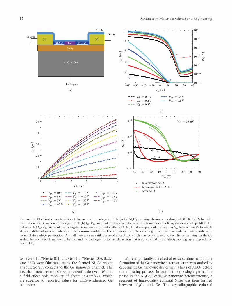
12 Advances in Materials Science and Engineering
n+-Si (100)
Al2O3
NixGe NixGe
SiO2
NiNiGe
Source
Back-gate
Drain
(a)
(μA
)
−40 −30 −20 −10 0 10 20 30 40
I(A
)
0
2
4
6
8
10
10−11
10−10
10−9
10−8
10−7
10−6
10−5
V = 0.1 VV = 0.2 VV = 0.3 V
V = 0.4 VV = 0.5 V
ds
dsds
ds
ds
Vgs (V)
I ds
ds
(b)
0 1 2 3 4 50
10
20
30
40
50
I(μ
A)
V (V)
V = 10 V
V = 0 V
V = −10 V
V = −20 V
V = −30 VV = −35 VV = −40 V
V = 5 V
V = −5 V
V = −15 V
V = −25 V
gs
gs
gs
gs gs
gs
gs
gs gs
gs
gs
ds
ds
(c)
−40 −30 −20 −10 0 10 20 30 4010−10
10−9
10−8
10−7V = 20 mV
In air before ALDIn vacuum before ALDAfter ALD
Vgs (V)
I(A
)ds
ds
(d)
Figure 10: Electrical characteristics of Ge nanowire back-gate FETs (with Al2O3 capping during annealing) at 300 K. (a) Schematicillustration of a Ge nanowire back-gate FET. (b) Ids-Vgs curves of the back-gate Ge nanowire transistor after RTA, showing a p-type MOSFETbehavior. (c) Ids-Vds curves of the back-gate Ge nanowire transistor after RTA. (d) Dual sweepings of the gate biasVgs between +40 V to−40 Vshowing different sizes of hysteresis under various conditions. The arrows indicate the sweeping directions. The hysteresis was significantlyreduced after Al2O3 passivation. A small hysteresis was still observed after ALD, which may be attributed to the charge trapping on the Gesurface between the Ge nanowire channel and the back-gate dielectric, the region that is not covered by the Al2O3 capping layer. Reproducedfrom [14].
to be Ge[011]//Ni2Ge[011] and Ge(11 1)//Ni2Ge(100). Back-gate FETs were fabricated using the formed Ni2Ge regionas source/drain contacts to the Ge nanowire channel. Theelectrical measurement shows an on/off ratio over 103 anda field-effect hole mobility of about 65.4 cm2/Vs, whichare superior to reported values for SFLS-synthesized Genanowires.
More importantly, the effect of oxide confinement on theformation of the Ge nanowire heterostructure was studied bycapping the Ge nanowire device with a layer of Al2O3 beforethe annealing process. In contrast to the single germanidephase in the Ni2Ge/Ge/Ni2Ge nanowire heterostructure, asegment of high-quality epitaxial NiGe was then formedbetween Ni2Ge and Ge. The crystallographic epitaxial
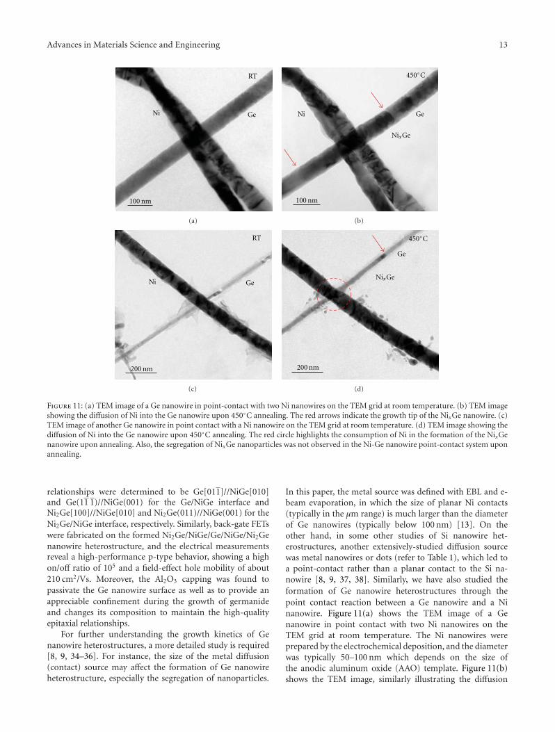
Advances in Materials Science and Engineering 13
100 nm
RT
GeNi
(a)
100 nm
GeNi
NixGe
450◦C
(b)
200 nm
RT
GeNi
(c)
200 nm
Ge
Ni NixGe
450◦C
(d)
Figure 11: (a) TEM image of a Ge nanowire in point-contact with two Ni nanowires on the TEM grid at room temperature. (b) TEM imageshowing the diffusion of Ni into the Ge nanowire upon 450◦C annealing. The red arrows indicate the growth tip of the NixGe nanowire. (c)TEM image of another Ge nanowire in point contact with a Ni nanowire on the TEM grid at room temperature. (d) TEM image showing thediffusion of Ni into the Ge nanowire upon 450◦C annealing. The red circle highlights the consumption of Ni in the formation of the NixGenanowire upon annealing. Also, the segregation of NixGe nanoparticles was not observed in the Ni-Ge nanowire point-contact system uponannealing.
relationships were determined to be Ge[011]//NiGe[010]and Ge(11 1)//NiGe(001) for the Ge/NiGe interface andNi2Ge[100]//NiGe[010] and Ni2Ge(011)//NiGe(001) for theNi2Ge/NiGe interface, respectively. Similarly, back-gate FETswere fabricated on the formed Ni2Ge/NiGe/Ge/NiGe/Ni2Genanowire heterostructure, and the electrical measurementsreveal a high-performance p-type behavior, showing a highon/off ratio of 105 and a field-effect hole mobility of about210 cm2/Vs. Moreover, the Al2O3 capping was found topassivate the Ge nanowire surface as well as to provide anappreciable confinement during the growth of germanideand changes its composition to maintain the high-qualityepitaxial relationships.
For further understanding the growth kinetics of Genanowire heterostructures, a more detailed study is required[8, 9, 34–36]. For instance, the size of the metal diffusion(contact) source may affect the formation of Ge nanowireheterostructure, especially the segregation of nanoparticles.
In this paper, the metal source was defined with EBL and e-beam evaporation, in which the size of planar Ni contacts(typically in the μm range) is much larger than the diameterof Ge nanowires (typically below 100 nm) [13]. On theother hand, in some other studies of Si nanowire het-erostructures, another extensively-studied diffusion sourcewas metal nanowires or dots (refer to Table 1), which led toa point-contact rather than a planar contact to the Si na-nowire [8, 9, 37, 38]. Similarly, we have also studied theformation of Ge nanowire heterostructures through thepoint contact reaction between a Ge nanowire and a Ninanowire. Figure 11(a) shows the TEM image of a Genanowire in point contact with two Ni nanowires on theTEM grid at room temperature. The Ni nanowires wereprepared by the electrochemical deposition, and the diameterwas typically 50–100 nm which depends on the size ofthe anodic aluminum oxide (AAO) template. Figure 11(b)shows the TEM image, similarly illustrating the diffusion
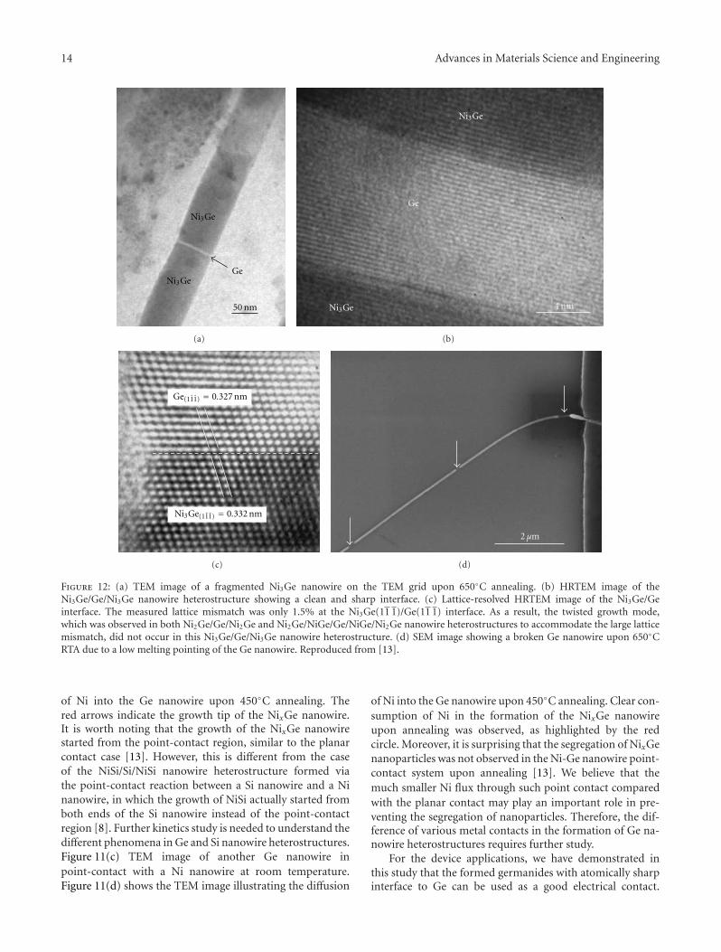
14 Advances in Materials Science and Engineering
50 nm
Ni3Ge
Ni3GeGe
(a)
Ni3Ge
Ni3Ge
Ge
4 nm
(b)
Ge(111) = 0.327 nm
Ni3Ge( ¯1 ¯11) = 0.332 nm
(c)
2 μm
(d)
Figure 12: (a) TEM image of a fragmented Ni3Ge nanowire on the TEM grid upon 650◦C annealing. (b) HRTEM image of theNi3Ge/Ge/Ni3Ge nanowire heterostructure showing a clean and sharp interface. (c) Lattice-resolved HRTEM image of the Ni3Ge/Geinterface. The measured lattice mismatch was only 1.5% at the Ni3Ge(11 1)/Ge(11 1) interface. As a result, the twisted growth mode,which was observed in both Ni2Ge/Ge/Ni2Ge and Ni2Ge/NiGe/Ge/NiGe/Ni2Ge nanowire heterostructures to accommodate the large latticemismatch, did not occur in this Ni3Ge/Ge/Ni3Ge nanowire heterostructure. (d) SEM image showing a broken Ge nanowire upon 650◦CRTA due to a low melting pointing of the Ge nanowire. Reproduced from [13].
of Ni into the Ge nanowire upon 450◦C annealing. Thered arrows indicate the growth tip of the NixGe nanowire.It is worth noting that the growth of the NixGe nanowirestarted from the point-contact region, similar to the planarcontact case [13]. However, this is different from the caseof the NiSi/Si/NiSi nanowire heterostructure formed viathe point-contact reaction between a Si nanowire and a Ninanowire, in which the growth of NiSi actually started fromboth ends of the Si nanowire instead of the point-contactregion [8]. Further kinetics study is needed to understand thedifferent phenomena in Ge and Si nanowire heterostructures.Figure 11(c) TEM image of another Ge nanowire inpoint-contact with a Ni nanowire at room temperature.Figure 11(d) shows the TEM image illustrating the diffusion
of Ni into the Ge nanowire upon 450◦C annealing. Clear con-sumption of Ni in the formation of the NixGe nanowireupon annealing was observed, as highlighted by the redcircle. Moreover, it is surprising that the segregation of NixGenanoparticles was not observed in the Ni-Ge nanowire point-contact system upon annealing [13]. We believe that themuch smaller Ni flux through such point contact comparedwith the planar contact may play an important role in pre-venting the segregation of nanoparticles. Therefore, the dif-ference of various metal contacts in the formation of Ge na-nowire heterostructures requires further study.
For the device applications, we have demonstrated inthis study that the formed germanides with atomically sharpinterface to Ge can be used as a good electrical contact.
Advances in Materials Science and Engineering 15
Indeed, Lin et al. [11] have successfully detected the electricalspin injection into a Si nanowire from the ferromagneticMnSi contact in the formed MnSi/Si/MnSi nanowire het-erostructure. However, the signal can be observed only atrelatively low temperature, since MnSi has a low Curie tem-perature of about 30 K. On the other hand, there are manygermanides, such as Mn5Ge3 and Ni3Ge, which exhibitroom-temperature ferromagnetism [20, 21], and thus offergreat advantages over silicides for promising applicationsin room-temperature spintronics, including spin injection,transport and detection.
In fact, a room-temperature ferromagnetic germanidephase, Ni3Ge [20], was developed at high reactiontemperature, in which a high-concentration Ni vaporfrom a large-area Ni contact pattern surrounded the GeNWs to form a fragmented Ni3Ge nanowire. Figure 12(a)shows the TEM image of the formed Ni3Ge/Ge/Ni3Genanowire heterostructure on the TEM grid upon650◦C annealing. Figure 12(b) illustrates the HRTEMimage of the Ge nanowire heterostructure with a cleanand sharp interface between Ni3Ge and Ge. The Geregion was controlled down to as small as 12 nm. Thestrained short Ge region in the Ni3Ge/Ge/Ni3Ge nanowireheterostructure is promising for high-performance FETsand spintronics applications [11, 39]. Figure 12(c) showsthe lattice-resolved TEM image of the Ni3Ge-Ge in-terface, and the formed germanide was identified to besingle-crystalline Ni3Ge with a face-centered cubic (FCC)lattice structure (Fd3m, space group 227 and JCPDS no.65-7680) and a lattice constant of a = 0.574 nm. Althougha slight volume expansion was still observed, the Ni3Gelattice was well fit with the Ge lattice, due to their samelattice structure and a very small lattice mismatch ofonly 1.5% (the lattice constant of Ge is a = 0.568 nm).It is worth mentioning that the twisted growth mode,which was observed in both Ni2Ge/Ge/Ni2Ge andNi2Ge/NiGe/Ge/NiGe/Ni2Ge nanowire heterostructuresto accommodate the large lattice mismatch, did not occur inthis Ni3Ge/Ge/Ni3Ge nanowire heterostructure due to sucha small lattice mismatch. However, as mentioned above,the melting point of Ge nanowires is significantly reducedfrom that of bulk Ge [29]. As a result, Ge nanowires wereeasily broken at high temperature, as shown in Figure 12(d).Therefore, a ferromagnetic germanide remains undevelopedat a relatively low temperature in order to study the spintransport in Ge nanowire.
Acknowledgments
This work was in part supported by Western Institution ofNanoelectronics (WIN) and Focus Center on FunctionalEngineered Nano Architectonics (FENA). The authors alsoacknowledged the support from National Science Councilthrough Grant no. NSC 98-2221-E-007-104-MY3. J. Tangand C. Y. Wang contributed equally to the paper.
References
[1] D. Wang, Q. Wang, A. Javey et al., “Germanium nanowirefield-effect transistors with SiO2 and high-κ HfO2 gatedielectrics,” Applied Physics Letters, vol. 83, no. 12, pp. 2432–2434, 2003.
[2] M. I. Van Der Meulen, N. Petkov, M. A. Morris et al., “Singlecrystalline Ge1−x Mnx nanowires as building blocks fornanoelectronics,” Nano Letters, vol. 9, no. 1, pp. 50–56, 2009.
[3] Y. Huang, X. Duan, Y. Cui, L. J. Lauhon, K. H. Kim, andC. M. Lieber, “Logic gates and computation from assemblednanowire building blocks,” Science, vol. 294, no. 5545, pp.1313–1317, 2001.
[4] C. Thelander, H. A. Nilsson, L. E. Jensen, and L. Samuelson,“Nanowire single-electron memory,” Nano Letters, vol. 5, no.4, pp. 635–638, 2005.
[5] Y. Cui, Q. Wei, H. Park, and C. M. Lieber, “Nanowire na-nosensors for highly sensitive and selective detection of bio-logical and chemical species,” Science, vol. 293, no. 5533, pp.1289–1292, 2001.
[6] Y. Wu, J. Xiang, C. Yang, W. Lu, and C. M. Lieber, “Single-crys-tal metallic nanowires and metal/semiconductor nanowireheterostructures,” Nature, vol. 430, no. 6995, pp. 61–65, 2004.
[7] W. M. Weber, L. Geelhaar, A. P. Graham et al., “Silicon-nanowire transistors with intruded nickel-suicide contacts,”Nano Letters, vol. 6, no. 12, pp. 2660–2666, 2006.
[8] K. C. Lu, W. W. Wu, H. W. Wu et al., “In situ control of atomic-scale Si layer with huge strain in the nanoheterostructureNiSi/Si/NiSi through point contact reaction,” Nano Letters,vol. 7, no. 8, pp. 2389–2394, 2007.
[9] Y. C. Chou, W. W. Wu, S. L. Cheng et al., “In-situ TEMObservation of repeating events of nucleation in epitaxialgrowth of nano CoSi2 in nanowires of Si,” Nano Letters, vol.8, no. 8, pp. 2194–2199, 2008.
[10] Y. C. Lin, K. C. Lu, W. W. Wu et al., “Single crystalline PtSinanowires, PtSi/Si/PtSi nanowire heterostructures, and nan-odevices,” Nano Letters, vol. 8, no. 3, pp. 913–918, 2008.
[11] Y. C. Lin, Y. Chen, A. Shailos, and Y. Huang, “Detection of spinpolarized carrier in silicon nanowire with single crystal MnSias magnetic contacts,” Nano Letters, vol. 10, no. 6, pp. 2281–2287, 2010.
[12] Y. Zhou, M. Ogawa, X. Han, and K. L. Wang, “Alleviationof Fermi-level pinning effect on metal/germanium interfaceby insertion of an ultrathin aluminum oxide,” Applied PhysicsLetters, vol. 93, no. 20, Article ID 202105, 2008.
[13] J. Tang, C. Y. Wang, F. Xiu et al., “Single-crystallineNi2Ge/Ge/Ni2Ge nanowire heterostructure transistors,” Nan-otechnology, vol. 21, no. 50, Article ID 505704, 2010.
[14] J. Tang, C. Y. Wang, F. Xiu et al., “Oxide-confined formationof Ge nanowire heterostructure for high-performance transis-tors,” ACS Nano, vol. 5, no. 7, pp. 6008–6015, 2011.
[15] N. S. Dellas, S. Minassian, J. M. Redwing, and S. E. Mohney,“Formation of nickel germanide contacts to Ge nanowires,”Applied Physics Letters, vol. 97, no. 26, Article ID 263116, 2010.
[16] T. Burchhart, A. Lugstein, Y. J. Hyun, G. Hochleitner, andE. Bertagnolli, “Atomic scale alignment of copper-germanidecontacts for ge nanowire metal oxide field effect transistors,”Nano Letters, vol. 9, no. 11, pp. 3739–3742, 2009.
[17] T. Burchhart, C. Zeiner, Y. J. Hyun, A. Lugstein, G. Hochleit-ner, and E. Bertagnolli, “High performance Ω-gated Genanowire MOSFET with quasi-metallic source/drain con-tacts,” Nanotechnology, vol. 21, no. 43, Article ID 435704, 2010.
[18] T. Burchhart, A. Lugstein, C. Zeiner, Y. J. Hyun, G. Hochleit-ner, and E. Bertagnolli, “Nanowire-metal heterostructures for
16 Advances in Materials Science and Engineering
high performance MOSFETs,” Elektrotechnik und Information-stechnik, vol. 127, no. 6, pp. 171–175, 2010.
[19] K. Yamane, K. Hamaya, Y. Ando et al., “Effect of atomicallycontrolled interfaces on Fermi-level pinning at metal/Geinterfaces,” Applied Physics Letters, vol. 96, no. 16, Article ID162104, 2010.
[20] T. Izumi, M. Taniguchi, S. Kumai, and A. Sato, “Ferromagneticproperties of cyclically deformed Fe3Ge and Ni3Ge,” Philo-sophical Magazine, vol. 84, no. 36, pp. 3883–3895, 2004.
[21] M. Jamet, A. Barski, T. Devillers et al., “High-curie-tem-perature ferromagnetism in self-organized Ge1−xMnx nano-columns,” Nature Materials, vol. 5, no. 8, pp. 653–659, 2006.
[22] H. Y. Tuan and B. A. Korgel, “Importance of solvent-mediatedphenylsilane decompositon kinetics for high-yield solution-phase silicon nanowire synthesis,” Chemistry of Materials, vol.20, no. 4, pp. 1239–1241, 2008.
[23] T. Hanrath and B. A. Korgel, “Supercritical fluid-liquid-solid(SFLS) synthesis of Si and Ge nanowires seeded by colloidalmetal nanocrystals,” Advanced Materials, vol. 15, no. 5, pp.437–440, 2003.
[24] Y. L. Chueh, C. N. Boswell, C. W. Yuan et al., “Nanoscalestructural engineering via phase segregation: Au-Ge system,”Nano Letters, vol. 10, no. 2, pp. 393–397, 2010.
[25] A. D. Schricker, S. V. Joshi, T. Hanrath, S. K. Banerjee, and B. A.Korgel, “Temperature dependence of the field effect mobilityof solution-grown germanium nanowires,” Journal of PhysicalChemistry B, vol. 110, no. 13, pp. 6816–6823, 2006.
[26] T. Hanrath and B. A. Korgel, “Influence of surface states onelectron transport through intrinsic Ge nanowires,” Journal ofPhysical Chemistry B, vol. 109, no. 12, pp. 5518–5524, 2005.
[27] S. Zhang, E. R. Hemesath, D. E. Perea, E. Wijaya, J. L. Lensch-Falk, and L. J. Lauhon, “Relative influence of surface states andbulk impurities on the electrical properties of Ge nanowires,”Nano Letters, vol. 9, no. 9, pp. 3268–3274, 2009.
[28] Y. F. Hsieh, L. J. Chen, E. D. Marshall, and S. S. Lau, “Partialepitaxial growth of Ni2Ge and NiGe on Ge(1 1 1),” Thin SolidFilms, vol. 162, pp. 287–294, 1988.
[29] Y. Wu and P. Yang, “Melting and welding semiconductornanowires in nanotubes,” Advanced Materials, vol. 13, no. 7,pp. 520–523, 2001.
[30] Y. C. Lin, Y. Chen, D. Xu, and Y. Huang, “Growth of nickelsilicides in Si and Si/SiOx core/shell nanowires,” Nano Letters,vol. 10, no. 11, pp. 4721–4726, 2010.
[31] Y. Zhou, W. Han, Y. Wang et al., “Investigating the origin ofFermi level pinning in Ge Schottky junctions using epitaxiallygrown ultrathin MgO films,” Applied Physics Letters, vol. 96,no. 10, Article ID 102103, 2010.
[32] S. Ramo, J. R. Whinnery, and T. V. Duzer, Fields and Waves inCommunication Electronics, John Wiley & Sons, New York, NY,USA, 3rd edition, 1994.
[33] D. Wang, Y. L. Chang, Q. Wang et al., “Surface chemistry andelectrical properties of germanium nanowires,” Journal of theAmerican Chemical Society, vol. 126, no. 37, pp. 11602–11611,2004.
[34] Y. C. Chou, W. W. Wu, L. J. Chen, and K. N. Tu, “Homoge-neous nucleation of epitaxial CoSi2 and NiSi in Si nanowires,”Nano Letters, vol. 9, no. 6, pp. 2337–2342, 2009.
[35] L. J. Chen and W. W. Wu, “In situ TEM investigation ofdynamical changes of nanostructures,” Materials Science andEngineering R, vol. 70, no. 3–6, pp. 303–319, 2010.
[36] Y. C. Chou, W. W. Wu, C. Y. Lee, C. Y. Liu, L. J. Chen, and K. N.Tu, “Heterogeneous and homogeneous nucleation of epitaxialNiSi2 in [1 1 0] Si nanowires,” Journal of Physical Chemistry C,vol. 115, no. 2, pp. 397–401, 2011.
[37] K. C. Lu, K. N. Tu, W. W. Wu, L. J. Chen, B. Y. Yoo, and N. V.Myung, “Point contact reactions between Ni and Si nanowiresand reactive epitaxial growth of axial nano-NiSi/Si,” AppliedPhysics Letters, vol. 90, no. 25, Article ID 253111, 2007.
[38] W. W. Wu, K. C. Lu, C. W. Wang et al., “Growth ofmultiple metal/semiconductor nanoheterostructures throughpoint and line contact reactions,” Nano Letters, vol. 10, no. 10,pp. 3984–3989, 2010.
[39] W. W. Wu, K. C. Lu, K. N. Chen et al., “Controlled large strainof Ni silicide/Si/Ni silicide nanowire heterostructures and theirelectron transport properties,” Applied Physics Letters, vol. 97,no. 20, Article ID 203110, 2010.
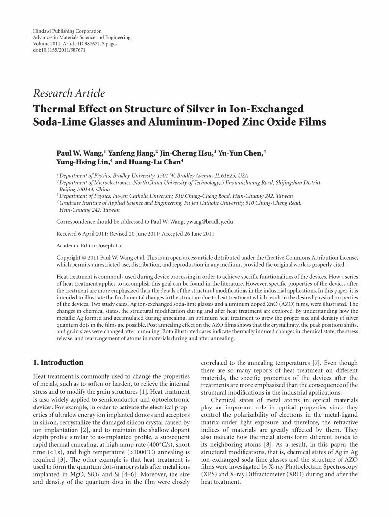
Hindawi Publishing CorporationAdvances in Materials Science and EngineeringVolume 2011, Article ID 987671, 7 pagesdoi:10.1155/2011/987671
Research Article
Thermal Effect on Structure of Silver in Ion-ExchangedSoda-Lime Glasses and Aluminum-Doped Zinc Oxide Films
Paul W. Wang,1 Yanfeng Jiang,2 Jin-Cherng Hsu,3 Yu-Yun Chen,4
Yung-Hsing Lin,4 and Huang-Lu Chen4
1 Department of Physics, Bradley University, 1501 W. Bradley Avenue, IL 61625, USA2 Department of Microelectronics, North China University of Technology, 5 Jinyuanzhuang Road, Shijingshan District,Beijing 100144, China
3 Department of Physics, Fu-Jen Catholic University, 510 Chung-Cheng Road, Hsin-Chuang 242, Taiwan4 Graduate Institute of Applied Science and Engineering, Fu Jen Catholic University, 510 Chung-Cheng Road,Hsin-Chuang 242, Taiwan
Correspondence should be addressed to Paul W. Wang, [email protected]
Received 6 April 2011; Revised 20 June 2011; Accepted 26 June 2011
Academic Editor: Joseph Lai
Copyright © 2011 Paul W. Wang et al. This is an open access article distributed under the Creative Commons Attribution License,which permits unrestricted use, distribution, and reproduction in any medium, provided the original work is properly cited.
Heat treatment is commonly used during device processing in order to achieve specific functionalities of the devices. How a seriesof heat treatment applies to accomplish this goal can be found in the literature. However, specific properties of the devices afterthe treatment are more emphasized than the details of the structural modifications in the industrial applications. In this paper, it isintended to illustrate the fundamental changes in the structure due to heat treatment which result in the desired physical propertiesof the devices. Two study cases, Ag ion-exchanged soda-lime glasses and aluminum doped ZnO (AZO) films, were illustrated. Thechanges in chemical states, the structural modification during and after heat treatment are explored. By understanding how themetallic Ag formed and accumulated during annealing, an optimum heat treatment to grow the proper size and density of silverquantum dots in the films are possible. Post annealing effect on the AZO films shows that the crystallinity, the peak positions shifts,and grain sizes were changed after annealing. Both illustrated cases indicate thermally induced changes in chemical state, the stressrelease, and rearrangement of atoms in materials during and after annealing.
1. Introduction
Heat treatment is commonly used to change the propertiesof metals, such as to soften or harden, to relieve the internalstress and to modify the grain structures [1]. Heat treatmentis also widely applied to semiconductor and optoelectronicdevices. For example, in order to activate the electrical prop-erties of ultralow energy ion implanted donors and acceptorsin silicon, recrystallize the damaged silicon crystal caused byion implantation [2], and to maintain the shallow dopantdepth profile similar to as-implanted profile, a subsequentrapid thermal annealing, at high ramp rate (400◦C/s), shorttime (<1 s), and high temperature (>1000◦C) annealing isrequired [3]. The other example is that heat treatment isused to form the quantum dots/nanocrystals after metal ionsimplanted in MgO, SiO2 and Si [4–6]. Moreover, the sizeand density of the quantum dots in the film were closely
correlated to the annealing temperatures [7]. Even thoughthere are so many reports of heat treatment on differentmaterials, the specific properties of the devices after thetreatments are more emphasized than the consequence of thestructural modifications in the industrial applications.
Chemical states of metal atoms in optical materialsplay an important role in optical properties since theycontrol the polarizability of electrons in the metal-ligandmatrix under light exposure and therefore, the refractiveindices of materials are greatly affected by them. Theyalso indicate how the metal atoms form different bonds toits neighboring atoms [8]. As a result, in this paper, thestructural modifications, that is, chemical states of Ag in Agion-exchanged soda-lime glasses and the structure of AZOfilms were investigated by X-ray Photoelectron Spectroscopy(XPS) and X-ray Diffractometer (XRD) during and after theheat treatment.
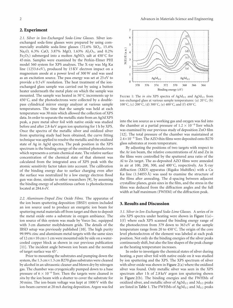
2 Advances in Materials Science and Engineering
2. Experiment
2.1. Silver in Ion-Exchanged Soda-Lime Glasses. Silver ion-exchanged soda-lime glasses were prepared by using com-mercially available soda-lime glasses (72.6% SiO2, 15.4%Na2O, 6.3% CaO, 3.87% MgO, 1.63% Al2O3, and 0.2%Fe2O3) submerged into a molten AgNO3 salt at 450◦C for45 min. Samples were examined by the Perkin-Elmer PHImodel 560 system for XPS analyses. The X-ray was Mg Kαline (1253.6 eV), produced by 15 KV electron impact on amagnesium anode at a power level of 300 W and was usedas an excitation source. The pass energy was set at 25 eV toprovide a 0.5 eV resolution. The heat treatment of the ion-exchanged glass sample was carried out by using a buttonheater underneath the metal plate on which the sample wasmounted. The sample was heated in 50◦C increments up to450◦C, and the photoelectrons were collected by a double-pass cylindrical mirror energy analyzer at various sampletemperatures. The time that the sample was held at eachtemperature was 30 min which allowed the collection of XPSdata. In order to separate the metallic state from an Ag3d XPSpeak, a pure metal silver foil with native oxide was studiedbefore and after 2.8-keV argon ion sputtering for 1 h by XPS.Once the spectra of the metallic silver and oxidized silverfrom sputtering study had been obtained, the curve fittingtechnique was applied to resolve the metallic and the oxidizedstate of Ag in Ag3d spectra. The peak position in the XPSspectrum is the binding energy of the emitted photoelectronwhich represents a certain chemical state. The relative surfaceconcentration of the chemical state of that element wascalculated from the integrated area of XPS peak with theatomic sensitivity factor taken into account. The calibrationof the binding energy due to surface charging even afterthe surface was neutralized by a low energy electron floodgun was done, similar to other researchers [9], by assumingthe binding energy of adventitious carbon 1s photoelectronslocated at 284.6 eV.
2.2. Aluminum-Doped Zinc Oxide Films. The apparatus ofthe ion beam sputtering deposition (IBSD) system includedan ion source used to produce an energetic ion beam forsputtering metal materials off from target and then to depositthe metal oxide onto a substrate in oxygen ambiance. Theion source of this system was made by Veeco Inc. equippedwith 3 cm diameter molybdenum grids. The details of theIBSD setup was previously published [10]. The high purity99.99% zinc and aluminum metal targets with the same sizesof 12 cm×10 cm×1 cm were mounted side by side on a water-cooled copper block as shown in our previous publication[11]. The incident angle between ion beam and the normalof target surface was 45◦.
Prior to mounting the substrates and pumping down thesystem, the 1.3 cm×1.3 cm B270 glass substrates were cleanedby alcohol in an ultrasonic cleaner and blown dry by nitrogengas. The chamber was cryogenically pumped down to a basepressure of 6 × 10⁻⁶ Torr. Then the targets were cleaned insitu by the ion beam with a shutter to cover the substrate for30 mins. The ion-beam voltage was kept at 1000 V with theion-beam current at 20 mA during deposition. Argon was fed
7
6
4
5
3
2
1
0
N(E
)/E
(a.u
.)
364366368370372374376378
Binding energy (eV)
Ag3d3/2 Ag3d5/2
(f)
(e)
(d)
(c)
(b)
(a)
Figure 1: The in situ XPS spectra of Ag3d3/2 and Ag3d5/2 fromion-exchanged glass at various sample temperatures: (a) 20◦C, (b)100◦C, (c) 200◦C, (d) 300◦C, (e) 400◦C, and (f) 450◦C.
into the ion source as a working gas and oxygen was fed intothe chamber at a partial pressure of 1.2 × 10⁻⁴ Torr whichwas examined by our previous study of deposition ZnO film[12]. The total pressure of the chamber was maintained at2.4×10−4 Torr. The AZO thin films were deposited onto B270glass substrates at room temperature.
By adjusting the positions of two targets with respect tothe Ar ion beam, the relative concentrations of Al and Zn inthe films were controlled by the sputtered area ratio of theAl to Zn target. The as-deposited AZO films were annealedin air at 100, 200, 300, and 400◦C, respectively. An X-raydiffraction (XRD) apparatus (Rigaku Multiflex) with a CuKα line (1.54055 A) was used to examine the structure ofthe films after annealing. The d-spacing between adjacentcrystalline planes, grain sizes in the film, and the stress in thefilms was deduced from the diffraction angles and the fullwidth at half maximum (FWHM) of the diffraction peak.
3. Results and Discussion
3.1. Silver in Ion-Exchanged Soda-Lime Glasses. A series of insitu XPS spectra under heating were shown in Figure 1(a)–1(f) where each XPS scanned the binding energy range ofthe photoelectron from 379 down to 363 eV at the sampletemperature range from 20 to 450◦C. The origin of the corelevel photoelectron of the element was labeled at each peakposition. Not only do the binding energies of the silver peakscontinuously shift, but also the line shapes of the peak changeas the heating temperature increases.
In order to investigate the chemical states of silver duringheating, a pure silver foil with native oxide on it was studiedby ion sputtering and the XPS. The XPS spectrum of silverwith silver oxide was shown in Figure 2(a) where the oxidizedsilver was found. Only metallic silver was seen in the XPSspectrum after 1 h of 2.8 keV argon ion sputtering shownin Figure 2(b). The binding energies and the FWHMs ofoxidized silver, and metallic silver of Ag3d5/2 and 3d3/2 peaksare listed in Table 1. The FWHMs of Ag3d3/2 and 3d5/2 peaks
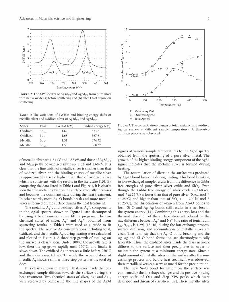
Advances in Materials Science and Engineering 3
7
6
5
4
3
2
1
0
N(E
)/E
364366368370372374376378
Binding energy (eV)
Ag3d3/2 Ag3d5/2
(b)
(a)
(a.u
.)
Figure 2: The XPS spectra of Ag3d3/2 and Ag3d5/2 from pure silverwith native oxide (a) before sputtering and (b) after 1 h of argon ionsputtering.
Table 1: The variations of FWHM and binding energy shifts ofmetallic silver and oxidized silver of Ag3d3/2 and Ag3d5/2.
States Peak FWHM (eV) Binding energy (eV)
Oxidized 3d3/2 1.62 373.61
Oxidized 3d5/2 1.68 367.61
Metallic 3d3/2 1.51 374.32
Metallic 3d5/2 1.55 368.32
of metallic silver are 1.51 eV and 1.55 eV, and those of Ag3d3/2
and 3d5/2 peaks of oxidized silver are 1.62 and 1.68 eV. It isclear that the line width of metallic silver is smaller than thatof oxidized silver, and the binding energy of metallic silveris approximately 0.6 eV higher than that of oxidized silverwhich is consistent with the results in the literature [13]. Bycomparing the data listed in Table 1 and Figure 1, it is clearlyseen that the metallic silver on the surface gradually increasesand becomes the dominant state during the heat treatment.In other words, more Ag–O bonds break and more metallicsilver is formed on the surface during the heat treatment.
The metallic, Ag◦, and oxidized silver, Ag+, componentsin the Ag3d spectra shown in Figure 1, are decomposedby using a best Gaussian curve fitting program. The twochemical states of silver, Ag◦ and Ag+, obtained fromsputtering results in Table 1 were used as a guide to fitthe spectra. The relative Ag concentrations including total,oxidized, and the metallic Ag during heating were calculatedand plotted in Figure 3. A three-step growth of total Ag onthe surface is clearly seen. Under 100◦C the growth rate islow, then the Ag grows rapidly until 350◦C, and finally itslows down. The oxidized Ag increases a little before 250◦Cand then decreases till 450◦C, while the accumulation ofmetallic Ag shows a similar three-step pattern as the total Agdoes.
It is clearly shown in Figure 1 that silver inside the ion-exchanged sample diffuses towards the surface during theheat treatment. Two chemical states of silver, Ag◦ and Ag+,were resolved by comparing the line shapes of the Ag3d
Metallic Ag (%)Oxidized Ag (%)Total Ag (%)
0 100 200 300 400 500
Temperature (◦C)
0
2
4
6
8
10
12
Con
cen
trat
ion
ofA
gsp
ecie
s(%
)Figure 3: The concentration changes of total, metallic, and oxidizedAg on surface at different sample temperatures. A three-stepdiffusion process was observed.
signals at various sample temperatures to the Ag3d spectraobtained from the sputtering of a pure silver metal. Thegrowth of the higher binding energy component of the Ag3dsignal indicates that the metallic silver is formed duringheating.
The accumulation of silver on the surface was producedby Ag–O bond breaking during heating. This bond breakingin ion-exchanged sample results from the difference in Gibbsfree energies of pure silver, silver oxide and SiO2. Eventhough the Gibbs free energy of silver oxide (−2.68 kcalmol−1 at 25◦C) is lower than that of pure silver (0 kcal mol−1
at 25◦C) and higher than that of SiO2 (∼ −200 kal mol−1
at 25◦C), the dissociation of oxygen from Ag–O bonds toform Si–O and Ag–Ag bonds still results in a net loss inthe system energy [14]. Combining this energy loss and thethermal relaxation of the surface stress introduced by thesize difference between Ag+ and Na+ (the ratio of ionic radii,rAg+ /rNa+ , is 1.29) [15, 16] during the ion-exchange process,surface diffusion, and accumulation of metallic silver areclear. That is to say that the Ag–O bond breaking and theAg–Ag and Si–O bond formation are thermodynamicallyfavorable. Thus, the oxidized silver inside the glass networkdiffuses to the surface and then precipitates in order tomaintain the system at a minimum energy state. Since aslight amount of metallic silver on the surface after the ion-exchange process and before heat treatment was observed,these metallic silvers can serve as nuclei for the precipitation.
The new Si–O bond formation on the surface wasconfirmed by the line shape changes and the positive bindingenergy shifts of O1s and Si2p XPS peaks which weredescribed and discussed elsewhere [17]. These metallic silver
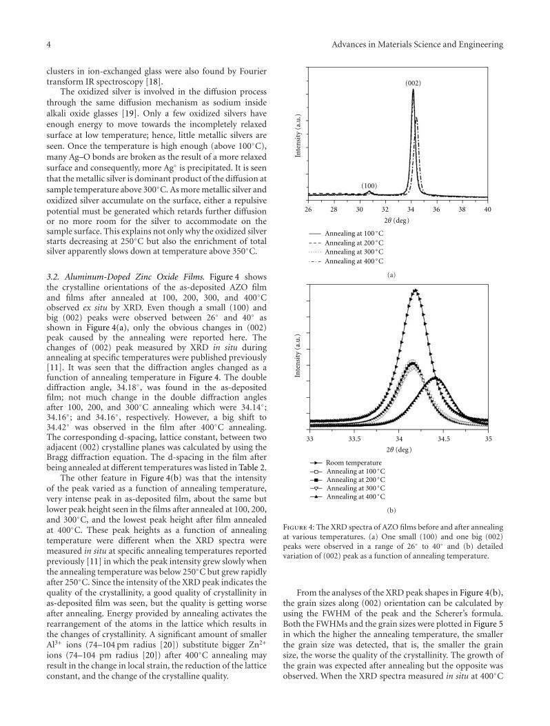
4 Advances in Materials Science and Engineering
clusters in ion-exchanged glass were also found by Fouriertransform IR spectroscopy [18].
The oxidized silver is involved in the diffusion processthrough the same diffusion mechanism as sodium insidealkali oxide glasses [19]. Only a few oxidized silvers haveenough energy to move towards the incompletely relaxedsurface at low temperature; hence, little metallic silvers areseen. Once the temperature is high enough (above 100◦C),many Ag–O bonds are broken as the result of a more relaxedsurface and consequently, more Ag◦ is precipitated. It is seenthat the metallic silver is dominant product of the diffusion atsample temperature above 300◦C. As more metallic silver andoxidized silver accumulate on the surface, either a repulsivepotential must be generated which retards further diffusionor no more room for the silver to accommodate on thesample surface. This explains not only why the oxidized silverstarts decreasing at 250◦C but also the enrichment of totalsilver apparently slows down at temperature above 350◦C.
3.2. Aluminum-Doped Zinc Oxide Films. Figure 4 showsthe crystalline orientations of the as-deposited AZO filmand films after annealed at 100, 200, 300, and 400◦Cobserved ex situ by XRD. Even though a small (100) andbig (002) peaks were observed between 26◦ and 40◦ asshown in Figure 4(a), only the obvious changes in (002)peak caused by the annealing were reported here. Thechanges of (002) peak measured by XRD in situ duringannealing at specific temperatures were published previously[11]. It was seen that the diffraction angles changed as afunction of annealing temperature in Figure 4. The doublediffraction angle, 34.18◦, was found in the as-depositedfilm; not much change in the double diffraction anglesafter 100, 200, and 300◦C annealing which were 34.14◦;34.16◦; and 34.16◦, respectively. However, a big shift to34.42◦ was observed in the film after 400◦C annealing.The corresponding d-spacing, lattice constant, between twoadjacent (002) crystalline planes was calculated by using theBragg diffraction equation. The d-spacing in the film afterbeing annealed at different temperatures was listed in Table 2.
The other feature in Figure 4(b) was that the intensityof the peak varied as a function of annealing temperature,very intense peak in as-deposited film, about the same butlower peak height seen in the films after annealed at 100, 200,and 300◦C, and the lowest peak height after film annealedat 400◦C. These peak heights as a function of annealingtemperature were different when the XRD spectra weremeasured in situ at specific annealing temperatures reportedpreviously [11] in which the peak intensity grew slowly whenthe annealing temperature was below 250◦C but grew rapidlyafter 250◦C. Since the intensity of the XRD peak indicates thequality of the crystallinity, a good quality of crystallinity inas-deposited film was seen, but the quality is getting worseafter annealing. Energy provided by annealing activates therearrangement of the atoms in the lattice which results inthe changes of crystallinity. A significant amount of smallerAl3+ ions (74–104 pm radius [20]) substitute bigger Zn2+
ions (74–104 pm radius [20]) after 400◦C annealing mayresult in the change in local strain, the reduction of the latticeconstant, and the change of the crystalline quality.
(002)
(100)
26 28 30 32 34 36 38 40
2θ (deg)
Inte
nsi
ty(a
.u.)
Annealing at 100◦CAnnealing at 200◦CAnnealing at 300◦CAnnealing at 400◦C
(a)
Inte
nsi
ty(a
.u.)
33 33.5 34 34.5 35
2θ (deg)
Room temperatureAnnealing at 100◦CAnnealing at 200◦CAnnealing at 300◦CAnnealing at 400◦C
(b)
Figure 4: The XRD spectra of AZO films before and after annealingat various temperatures. (a) One small (100) and one big (002)peaks were observed in a range of 26◦ to 40◦ and (b) detailedvariation of (002) peak as a function of annealing temperature.
From the analyses of the XRD peak shapes in Figure 4(b),the grain sizes along (002) orientation can be calculated byusing the FWHM of the peak and the Scherer’s formula.Both the FWHMs and the grain sizes were plotted in Figure 5in which the higher the annealing temperature, the smallerthe grain size was detected, that is, the smaller the grainsize, the worse the quality of the crystallinity. The growth ofthe grain was expected after annealing but the opposite wasobserved. When the XRD spectra measured in situ at 400◦C
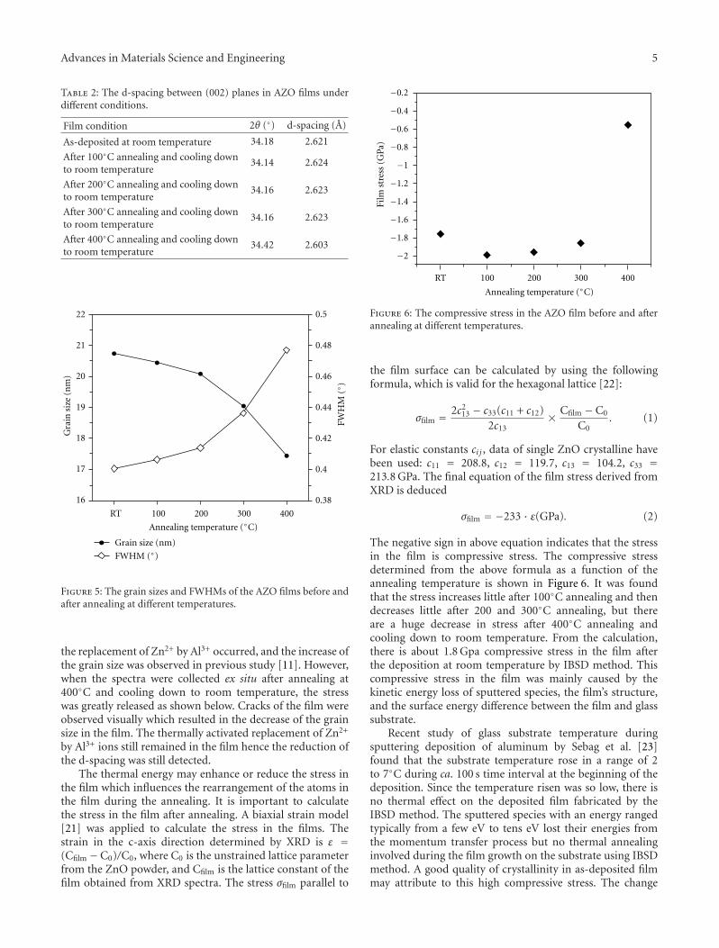
Advances in Materials Science and Engineering 5
Table 2: The d-spacing between (002) planes in AZO films underdifferent conditions.
Film condition 2θ (◦) d-spacing (A)
As-deposited at room temperature 34.18 2.621
After 100◦C annealing and cooling downto room temperature
34.14 2.624
After 200◦C annealing and cooling downto room temperature
34.16 2.623
After 300◦C annealing and cooling downto room temperature
34.16 2.623
After 400◦C annealing and cooling downto room temperature
34.42 2.603
16
17
18
19
20
21
22
RT 100 200 300 400
0.5
0.48
0.46
0.44
0.42
0.4
0.38
Gra
insi
ze(n
m)
FWH
M(◦
)
Annealing temperature (◦C)
Grain size (nm)
FWHM (◦)
Figure 5: The grain sizes and FWHMs of the AZO films before andafter annealing at different temperatures.
the replacement of Zn2+ by Al3+ occurred, and the increase ofthe grain size was observed in previous study [11]. However,when the spectra were collected ex situ after annealing at400◦C and cooling down to room temperature, the stresswas greatly released as shown below. Cracks of the film wereobserved visually which resulted in the decrease of the grainsize in the film. The thermally activated replacement of Zn2+
by Al3+ ions still remained in the film hence the reduction ofthe d-spacing was still detected.
The thermal energy may enhance or reduce the stress inthe film which influences the rearrangement of the atoms inthe film during the annealing. It is important to calculatethe stress in the film after annealing. A biaxial strain model[21] was applied to calculate the stress in the films. Thestrain in the c-axis direction determined by XRD is ε =(Cfilm −C0)/C0, where C0 is the unstrained lattice parameterfrom the ZnO powder, and Cfilm is the lattice constant of thefilm obtained from XRD spectra. The stress σfilm parallel to
−2
−1.8
−1.6
−1.4
−1.2
−1
−0.8
−0.6
−0.4
−0.2
RT 100 200 300 400
Annealing temperature (◦C)
Film
stre
ss(G
Pa)
Figure 6: The compressive stress in the AZO film before and afterannealing at different temperatures.
the film surface can be calculated by using the followingformula, which is valid for the hexagonal lattice [22]:
σfilm = 2c213 − c33(c11 + c12)
2c13× Cfilm − C0
C0. (1)
For elastic constants ci j , data of single ZnO crystalline havebeen used: c11 = 208.8, c12 = 119.7, c13 = 104.2, c33 =213.8 GPa. The final equation of the film stress derived fromXRD is deduced
σfilm = −233 · ε(GPa). (2)
The negative sign in above equation indicates that the stressin the film is compressive stress. The compressive stressdetermined from the above formula as a function of theannealing temperature is shown in Figure 6. It was foundthat the stress increases little after 100◦C annealing and thendecreases little after 200 and 300◦C annealing, but thereare a huge decrease in stress after 400◦C annealing andcooling down to room temperature. From the calculation,there is about 1.8 Gpa compressive stress in the film afterthe deposition at room temperature by IBSD method. Thiscompressive stress in the film was mainly caused by thekinetic energy loss of sputtered species, the film’s structure,and the surface energy difference between the film and glasssubstrate.
Recent study of glass substrate temperature duringsputtering deposition of aluminum by Sebag et al. [23]found that the substrate temperature rose in a range of 2to 7◦C during ca. 100 s time interval at the beginning of thedeposition. Since the temperature risen was so low, there isno thermal effect on the deposited film fabricated by theIBSD method. The sputtered species with an energy rangedtypically from a few eV to tens eV lost their energies fromthe momentum transfer process but no thermal annealinginvolved during the film growth on the substrate using IBSDmethod. A good quality of crystallinity in as-deposited filmmay attribute to this high compressive stress. The change
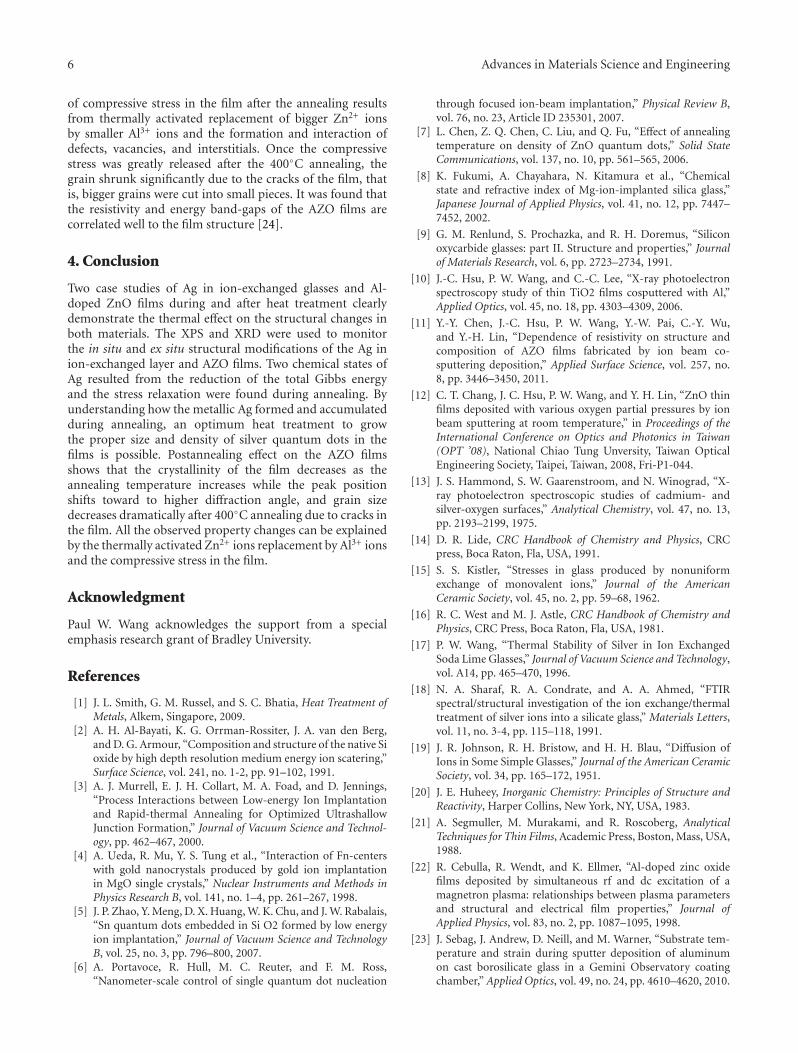
6 Advances in Materials Science and Engineering
of compressive stress in the film after the annealing resultsfrom thermally activated replacement of bigger Zn2+ ionsby smaller Al3+ ions and the formation and interaction ofdefects, vacancies, and interstitials. Once the compressivestress was greatly released after the 400◦C annealing, thegrain shrunk significantly due to the cracks of the film, thatis, bigger grains were cut into small pieces. It was found thatthe resistivity and energy band-gaps of the AZO films arecorrelated well to the film structure [24].
4. Conclusion
Two case studies of Ag in ion-exchanged glasses and Al-doped ZnO films during and after heat treatment clearlydemonstrate the thermal effect on the structural changes inboth materials. The XPS and XRD were used to monitorthe in situ and ex situ structural modifications of the Ag inion-exchanged layer and AZO films. Two chemical states ofAg resulted from the reduction of the total Gibbs energyand the stress relaxation were found during annealing. Byunderstanding how the metallic Ag formed and accumulatedduring annealing, an optimum heat treatment to growthe proper size and density of silver quantum dots in thefilms is possible. Postannealing effect on the AZO filmsshows that the crystallinity of the film decreases as theannealing temperature increases while the peak positionshifts toward to higher diffraction angle, and grain sizedecreases dramatically after 400◦C annealing due to cracks inthe film. All the observed property changes can be explainedby the thermally activated Zn2+ ions replacement by Al3+ ionsand the compressive stress in the film.
Acknowledgment
Paul W. Wang acknowledges the support from a specialemphasis research grant of Bradley University.
References
[1] J. L. Smith, G. M. Russel, and S. C. Bhatia, Heat Treatment ofMetals, Alkem, Singapore, 2009.
[2] A. H. Al-Bayati, K. G. Orrman-Rossiter, J. A. van den Berg,and D. G. Armour, “Composition and structure of the native Sioxide by high depth resolution medium energy ion scatering,”Surface Science, vol. 241, no. 1-2, pp. 91–102, 1991.
[3] A. J. Murrell, E. J. H. Collart, M. A. Foad, and D. Jennings,“Process Interactions between Low-energy Ion Implantationand Rapid-thermal Annealing for Optimized UltrashallowJunction Formation,” Journal of Vacuum Science and Technol-ogy, pp. 462–467, 2000.
[4] A. Ueda, R. Mu, Y. S. Tung et al., “Interaction of Fn-centerswith gold nanocrystals produced by gold ion implantationin MgO single crystals,” Nuclear Instruments and Methods inPhysics Research B, vol. 141, no. 1–4, pp. 261–267, 1998.
[5] J. P. Zhao, Y. Meng, D. X. Huang, W. K. Chu, and J. W. Rabalais,“Sn quantum dots embedded in Si O2 formed by low energyion implantation,” Journal of Vacuum Science and TechnologyB, vol. 25, no. 3, pp. 796–800, 2007.
[6] A. Portavoce, R. Hull, M. C. Reuter, and F. M. Ross,“Nanometer-scale control of single quantum dot nucleation
through focused ion-beam implantation,” Physical Review B,vol. 76, no. 23, Article ID 235301, 2007.
[7] L. Chen, Z. Q. Chen, C. Liu, and Q. Fu, “Effect of annealingtemperature on density of ZnO quantum dots,” Solid StateCommunications, vol. 137, no. 10, pp. 561–565, 2006.
[8] K. Fukumi, A. Chayahara, N. Kitamura et al., “Chemicalstate and refractive index of Mg-ion-implanted silica glass,”Japanese Journal of Applied Physics, vol. 41, no. 12, pp. 7447–7452, 2002.
[9] G. M. Renlund, S. Prochazka, and R. H. Doremus, “Siliconoxycarbide glasses: part II. Structure and properties,” Journalof Materials Research, vol. 6, pp. 2723–2734, 1991.
[10] J.-C. Hsu, P. W. Wang, and C.-C. Lee, “X-ray photoelectronspectroscopy study of thin TiO2 films cosputtered with Al,”Applied Optics, vol. 45, no. 18, pp. 4303–4309, 2006.
[11] Y.-Y. Chen, J.-C. Hsu, P. W. Wang, Y.-W. Pai, C.-Y. Wu,and Y.-H. Lin, “Dependence of resistivity on structure andcomposition of AZO films fabricated by ion beam co-sputtering deposition,” Applied Surface Science, vol. 257, no.8, pp. 3446–3450, 2011.
[12] C. T. Chang, J. C. Hsu, P. W. Wang, and Y. H. Lin, “ZnO thinfilms deposited with various oxygen partial pressures by ionbeam sputtering at room temperature,” in Proceedings of theInternational Conference on Optics and Photonics in Taiwan(OPT ’08), National Chiao Tung Unversity, Taiwan OpticalEngineering Society, Taipei, Taiwan, 2008, Fri-P1-044.
[13] J. S. Hammond, S. W. Gaarenstroom, and N. Winograd, “X-ray photoelectron spectroscopic studies of cadmium- andsilver-oxygen surfaces,” Analytical Chemistry, vol. 47, no. 13,pp. 2193–2199, 1975.
[14] D. R. Lide, CRC Handbook of Chemistry and Physics, CRCpress, Boca Raton, Fla, USA, 1991.
[15] S. S. Kistler, “Stresses in glass produced by nonuniformexchange of monovalent ions,” Journal of the AmericanCeramic Society, vol. 45, no. 2, pp. 59–68, 1962.
[16] R. C. West and M. J. Astle, CRC Handbook of Chemistry andPhysics, CRC Press, Boca Raton, Fla, USA, 1981.
[17] P. W. Wang, “Thermal Stability of Silver in Ion ExchangedSoda Lime Glasses,” Journal of Vacuum Science and Technology,vol. A14, pp. 465–470, 1996.
[18] N. A. Sharaf, R. A. Condrate, and A. A. Ahmed, “FTIRspectral/structural investigation of the ion exchange/thermaltreatment of silver ions into a silicate glass,” Materials Letters,vol. 11, no. 3-4, pp. 115–118, 1991.
[19] J. R. Johnson, R. H. Bristow, and H. H. Blau, “Diffusion ofIons in Some Simple Glasses,” Journal of the American CeramicSociety, vol. 34, pp. 165–172, 1951.
[20] J. E. Huheey, Inorganic Chemistry: Principles of Structure andReactivity, Harper Collins, New York, NY, USA, 1983.
[21] A. Segmuller, M. Murakami, and R. Roscoberg, AnalyticalTechniques for Thin Films, Academic Press, Boston, Mass, USA,1988.
[22] R. Cebulla, R. Wendt, and K. Ellmer, “Al-doped zinc oxidefilms deposited by simultaneous rf and dc excitation of amagnetron plasma: relationships between plasma parametersand structural and electrical film properties,” Journal ofApplied Physics, vol. 83, no. 2, pp. 1087–1095, 1998.
[23] J. Sebag, J. Andrew, D. Neill, and M. Warner, “Substrate tem-perature and strain during sputter deposition of aluminumon cast borosilicate glass in a Gemini Observatory coatingchamber,” Applied Optics, vol. 49, no. 24, pp. 4610–4620, 2010.

Advances in Materials Science and Engineering 7
[24] Y.-Y. Chen, J.-C. Hsu, C.-Y. Lee, and P. W. Wang, “Post-annealing Properties of Aluminum Doped Zinc Oxide FilmsFabricated by Ion Beam Co-sputtering,” in Proceedings ofthe 11th International Symposium on Sputtering and Plasma,Kyoto, Japan, July 2011.
Hindawi Publishing CorporationAdvances in Materials Science and EngineeringVolume 2011, Article ID 430604, 6 pagesdoi:10.1155/2011/430604
Research Article
The Effects of Different Types of Fly Ash onthe Compressive Strength Properties of Briquettes
Ozlem Celik Sola,1 Murat Yayla,2 Barıs Sayın,3 and Cengiz Duran Atis4
1 Civil Engineering Department, Engineering Faculty, Istanbul University, Avcılar Campus, Avcılar, Istanbul, Turkey2 Yapi Insaat Ltd. Co., Istanbul, Turkey3 Building and Technical Office, Istanbul University, Beyazıt Campus, Istanbul, Turkey4 Civil Engineering Department, Engineering and Architecture Faculty, Abdullah Gul University, Kayseri, Turkey
Correspondence should be addressed to Ozlem Celik Sola, [email protected]
Received 10 May 2011; Accepted 9 July 2011
Academic Editor: Kin Ho Lo
Copyright © 2011 Ozlem Celik Sola et al. This is an open access article distributed under the Creative Commons AttributionLicense, which permits unrestricted use, distribution, and reproduction in any medium, provided the original work is properlycited.
The aim of this study is to evaluate the effect of the different types of fly ash on the compressive strength properties of sinteredbriquettes. Thermal gravimetric (TG) analysis was carried out. The chemical composition and physical properties of the materialsused were determined. Particle size distribution and microstructure elemental analyses of the materials used were carried outby a particle size analyzer (Mastersizer) and a scanning electron microscope (SEM-EDS). Following the characterization of thematerials, briquettes were prepared by sintering at different temperatures. Compressive strength test results of the briquette samplesindicated that briquettes with a compressive strength value of 47.45 N/mm2 can be produced. The results obtained exceed theTurkish standard (TS EN 771-1) requirements (9.8–23.54 N/mm2). SEM-EDS results showed that briquette samples made withTuncbilek (T) fly ash had a higher percentage of the glassy phase than the other briquette samples. Due to this microstructure, itresults in higher compressive strength value.
1. Introduction
As an industrial waste, fly ash presents some environmentaland storage problems; however, it has been used widely asan excellent mineral additive in the construction industry[1, 2]. The use of fly ash prevents environmental pollution,and it contributes to a reduced need for natural resources.Fly ash is available in different types, such as C and F. The Ftype has a low Ca content, and its content of SiO2 + Fe2O3
+ Al2O3 is greater than 70 (ASTM C 618) [3]. There aremany studies investigating fly ash and its use as an additivein cement mortars [4, 5]. Fly ash is also used as an additivein the production of briquettes [6–11]. This study presentscomprehensive details about the utilization of different typesof fly ash that were collected from different thermal powerplants (Cayırhan, Orhaneli, Seyitomer, and Tuncbilek) inTurkey and that were used to produce briquettes that havehigh compressive strength values.
2. Materials and Methods
2.1. Properties of Materials Used
2.1.1. Soil. The soil was obtained from the Boyabat BrickFactory in Turkey. Its specific surface area was 0.7502 m2/g,and its chemical properties are given in Table 1. It had a highSiO2 content (51.21%).
2.1.2. Fly Ash. Four samples of fly ash were collected fromthe Cayırhan (C), Orhaneli (OE), Seyitomer (SO), andTuncbilek (T) thermal power plants in Turkey, which arerecycling materials for evaluation as additive materials inthe building sector. Their specific surface areas are 0.5957,0.8731, 0.4420, and 1.2769 m2/g, respectively. The chemicalanalysis results of the fly ashes are given in Table 1. Accordingto ASTM 618, the SiO2+ Al2O3+ Fe2O3 values indicated that
2 Advances in Materials Science and Engineering
Table 1: The chemical composition (%w/w) of the materials used.
Constituents (%) Soil C OE SO T
SiO2 51.21 44.05 43.18 53.32 58.36
Al2O3 12.59 11.57 19.36 20.16 22.17
Fe2O3 2.66 8.81 7.71 10.50 7.09
CaO 7.04 14.19 17.84 4.40 2.61
MgO 3.31 4.97 2.80 4.50 2.46
K2O 1.70 1.80 1.64 2.98 2.27
Na2O 1.52 3.59 0.36 0.51 0.71
SO3 5.57 10.34 2.53 1.04 0.34
KK 12.00 1.39 4.00 1.65 3.35
F CaO 0.07 0.14 0.31 — 0.01
Cl− 0.0085 — — — —
Table 2: Content of the soil sample.
Content %w/w
Gravel 0.0
Sand 24.1
Silt 63.4
Clay 12.5
the fly ash sample obtained from the (C) thermal power plantshould be classified as type C and the (OE), (SO), and (T) flyash samples should be classified as type F.
2.1.3. Experimental Program. In order to prepare the bri-quette specimens from the materials, characterization exper-iments were carried out. A physical analysis of the soil wasperformed to determine the percentage of sand and gravelpresent. In addition to the physical analysis, a hydrometeranalysis was applied to the mass of the soil that passedthrough sieve No. 200 in order to separate the silt andclay materials. Tests of the consistency limits of the soil—the plastic limit, the liquid limit, and the plasticity index(PI)—were conducted. In order to determine the thermalbehavior of the soil, a TG analysis was carried out with aTGA-50. The particle size distribution of the materials wasmeasured by the Mastersizer-x technique (Malvern, MS-X1995 model). In order to describe the microstructure and toconduct an elemental analysis of the materials and briquettes,the SEM-EDS technique (JSM-5910LV, EDS Model: Oxford-Inca-7274) was used. The compressive strength resultswere explained by using the results obtained from theseanalyses.
2.1.4. Preparation and Testing of Briquettes. Following thecharacterization tests, different mixtures were prepared fromfly ash samples. Fly ash was added to the soil in ratios of 5%and 10%. Each mixture was treated with 6% water to providesufficient plasticity. At the end of this procedure, the mixtureswere squeezed at 200 kgf/cm2, and the samples were molded
Table 3: Test of consistency limits of the soil sample.
Limits %
Liquid 37.5
Plastic 23.4
Plasticity index 14.1
Table 4: Granulometric data for the materials used in experimentsand their size fractions.
Percentages % of particles with diameter
Materials d(0.10) (μm) d(0.50) (μm) d(0.90) (μm)
S 2.83 17.44 73.41
C 3.70 27.23 129.95
OE 3.43 21.18 77.71
SO 6.16 29.76 96.86
T 1.99 13.76 52.39
for sintering. Before sintering, the moisture in the mixtureswas evaporated in an oven at 105◦C. The remolded mixtureshad dimensions of 3.6 × 3.6 cm2, and they were sintered at850, 900, and 950◦C in the laboratory oven. After the ovenhad reached the required temperature, the briquettes wereremoved from the oven. The briquettes produced with thisprocess were tested for compressive strength according to theTurkish standards (TS EN 771-1) [12].
3. Results and Discussion
3.1. Characterization of the Materials
3.1.1. Hydrometer Analysis. A hydrometer analysis was car-ried out to obtain the soil content, which was found to be24.1% sand, 63.4% silt, and 12.5% clay. The findings arelisted in Table 2. The results of the tests of the consistencylimits of the soil are given in Table 3: a 37.5% liquid limit, a23.4% plastic limit, and a 14.1% plasticity index. From thetest results, it can be concluded that the soil is suitable forbrick production according to the American Association ofState Highway and Transportation Officials (AASHTO).
3.1.2. Particle Size Distribution. The Mastersizer-x techniquewas used for measuring the particle size distribution. Granu-lometric data for the S showed that the d(90) and d(50) valueswere 73.41 and 17.44 μm. Granulometric data for the sizefractions of the C, OE, SO, and T fly ash is displayed inTable 4; the d(90) and d(50) values were 129.95 and 27.23,77.71, and 21.18, 96.86, and 29.76 and 52.39 and 13.76 μm,respectively. The particle size ranged from 3 μm to well over129 μm for the materials. It can be observed that there aresignificant differences in the particle size distributions ofthe two samples of C and T for d(90): 129.95 and 52.39 μm,respectively. It can also be observed from the granulometricdata that T was the finest fly ash.
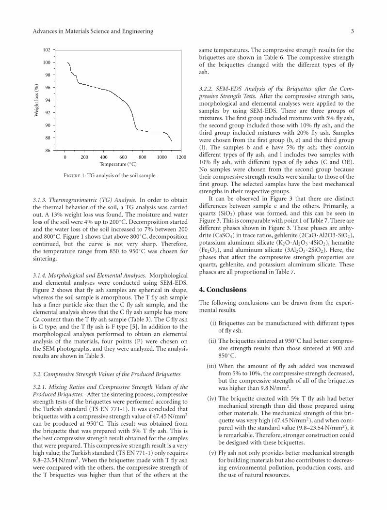
Advances in Materials Science and Engineering 3
0 200 400 600 800 1000 120086
88
90
92
94
96
98
100
102
Wei
ght
loss
(%
)
Temperature (◦C)
Figure 1: TG analysis of the soil sample.
3.1.3. Thermogravimetric (TG) Analysis. In order to obtainthe thermal behavior of the soil, a TG analysis was carriedout. A 13% weight loss was found. The moisture and waterloss of the soil were 4% up to 200◦C. Decomposition startedand the water loss of the soil increased to 7% between 200and 800◦C. Figure 1 shows that above 800◦C, decompositioncontinued, but the curve is not very sharp. Therefore,the temperature range from 850 to 950◦C was chosen forsintering.
3.1.4. Morphological and Elemental Analyses. Morphologicaland elemental analyses were conducted using SEM-EDS.Figure 2 shows that fly ash samples are spherical in shape,whereas the soil sample is amorphous. The T fly ash samplehas a finer particle size than the C fly ash sample, and theelemental analysis shows that the C fly ash sample has moreCa content than the T fly ash sample (Table 3). The C fly ashis C type, and the T fly ash is F type [5]. In addition to themorphological analyses performed to obtain an elementalanalysis of the materials, four points (P) were chosen onthe SEM photographs, and they were analyzed. The analysisresults are shown in Table 5.
3.2. Compressive Strength Values of the Produced Briquettes
3.2.1. Mixing Ratios and Compressive Strength Values of theProduced Briquettes. After the sintering process, compressivestrength tests of the briquettes were performed according tothe Turkish standard (TS EN 771-1). It was concluded thatbriquettes with a compressive strength value of 47.45 N/mm2
can be produced at 950◦C. This result was obtained fromthe briquette that was prepared with 5% T fly ash. This isthe best compressive strength result obtained for the samplesthat were prepared. This compressive strength result is a veryhigh value; the Turkish standard (TS EN 771-1) only requires9.8–23.54 N/mm2. When the briquettes made with T fly ashwere compared with the others, the compressive strength ofthe T briquettes was higher than that of the others at the
same temperatures. The compressive strength results for thebriquettes are shown in Table 6. The compressive strengthof the briquettes changed with the different types of flyash.
3.2.2. SEM-EDS Analysis of the Briquettes after the Com-pressive Strength Tests. After the compressive strength tests,morphological and elemental analyses were applied to thesamples by using SEM-EDS. There are three groups ofmixtures. The first group included mixtures with 5% fly ash,the second group included those with 10% fly ash, and thethird group included mixtures with 20% fly ash. Sampleswere chosen from the first group (b, e) and the third group(l). The samples b and e have 5% fly ash; they containdifferent types of fly ash, and l includes two samples with10% fly ash, with different types of fly ashes (C and OE).No samples were chosen from the second group becausetheir compressive strength results were similar to those of thefirst group. The selected samples have the best mechanicalstrengths in their respective groups.
It can be observed in Figure 3 that there are distinctdifferences between sample e and the others. Primarily, aquartz (SiO2) phase was formed, and this can be seen inFigure 3. This is comparable with point 1 of Table 7. There aredifferent phases shown in Figure 3. These phases are anhy-drite (CaSO4) in trace ratios, gehlenite (2CaO·Al2O3·SiO2),potassium aluminum silicate (K2O·Al2O3·4SiO2), hematite(Fe2O3), and aluminum silicate (3Al2O3·2SiO2). Here, thephases that affect the compressive strength properties arequartz, gehlenite, and potassium aluminum silicate. Thesephases are all proportional in Table 7.
4. Conclusions
The following conclusions can be drawn from the experi-mental results.
(i) Briquettes can be manufactured with different typesof fly ash.
(ii) The briquettes sintered at 950◦C had better compres-sive strength results than those sintered at 900 and850◦C.
(iii) When the amount of fly ash added was increasedfrom 5% to 10%, the compressive strength decreased,but the compressive strength of all of the briquetteswas higher than 9.8 N/mm2.
(iv) The briquette created with 5% T fly ash had bettermechanical strength than did those prepared usingother materials. The mechanical strength of this bri-quette was very high (47.45 N/mm2), and when com-pared with the standard value (9.8–23.54 N/mm2), itis remarkable. Therefore, stronger construction couldbe designed with these briquettes.
(v) Fly ash not only provides better mechanical strengthfor building materials but also contributes to decreas-ing environmental pollution, production costs, andthe use of natural resources.
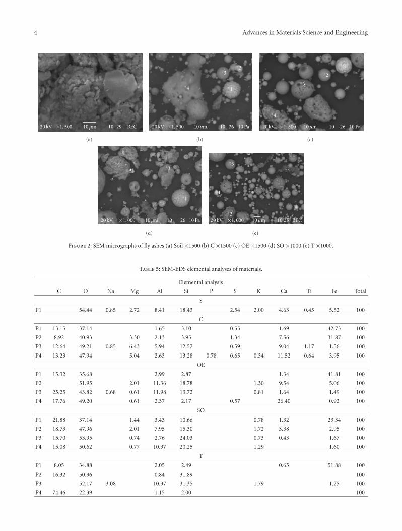
4 Advances in Materials Science and Engineering
20 kV ×1, 500 10 μm 10 29 BEC
(a)
◦3◦2
◦1◦4
20 kV ×1, 500 10 μm 10 26 10 Pa
(b)
◦3
◦2
◦1
◦4
20 kV ×1, 500 10 μm 10 10 Pa26
(c)
◦3
◦2◦1
◦4
20 kV 10 μm 10 10 Pa×1, 000 26
(d)
◦3
◦2
◦1
◦4
20 kV 10 μm 10 BEC×1, 000 25
(e)
Figure 2: SEM micrographs of fly ashes (a) Soil ×1500 (b) C ×1500 (c) OE ×1500 (d) SO ×1000 (e) T ×1000.
Table 5: SEM-EDS elemental analyses of materials.
Elemental analysis
C O Na Mg Al Si P S K Ca Ti Fe Total
S
P1 54.44 0.85 2.72 8.41 18.43 2.54 2.00 4.63 0.45 5.52 100
C
P1 13.15 37.14 1.65 3.10 0.55 1.69 42.73 100
P2 8.92 40.93 3.30 2.13 3.95 1.34 7.56 31.87 100
P3 12.64 49.21 0.85 6.43 5.94 12.57 0.59 9.04 1.17 1.56 100
P4 13.23 47.94 5.04 2.63 13.28 0.78 0.65 0.34 11.52 0.64 3.95 100
OE
P1 15.32 35.68 2.99 2.87 1.34 41.81 100
P2 51.95 2.01 11.36 18.78 1.30 9.54 5.06 100
P3 25.25 43.82 0.68 0.61 11.98 13.72 0.81 1.64 1.49 100
P4 17.76 49.20 0.61 2.37 2.17 0.57 26.40 0.92 100
SO
P1 21.88 37.14 1.44 3.43 10.66 0.78 1.32 23.34 100
P2 18.73 47.96 2.01 7.95 15.30 1.72 3.38 2.95 100
P3 15.70 53.95 0.74 2.76 24.03 0.73 0.43 1.67 100
P4 15.08 50.62 0.77 10.37 20.25 1.29 1.60 100
T
P1 8.05 34.88 2.05 2.49 0.65 51.88 100
P2 16.32 50.96 0.84 31.89 100
P3 52.17 3.08 10.37 31.35 1.79 1.25 100
P4 74.46 22.39 1.15 2.00 100
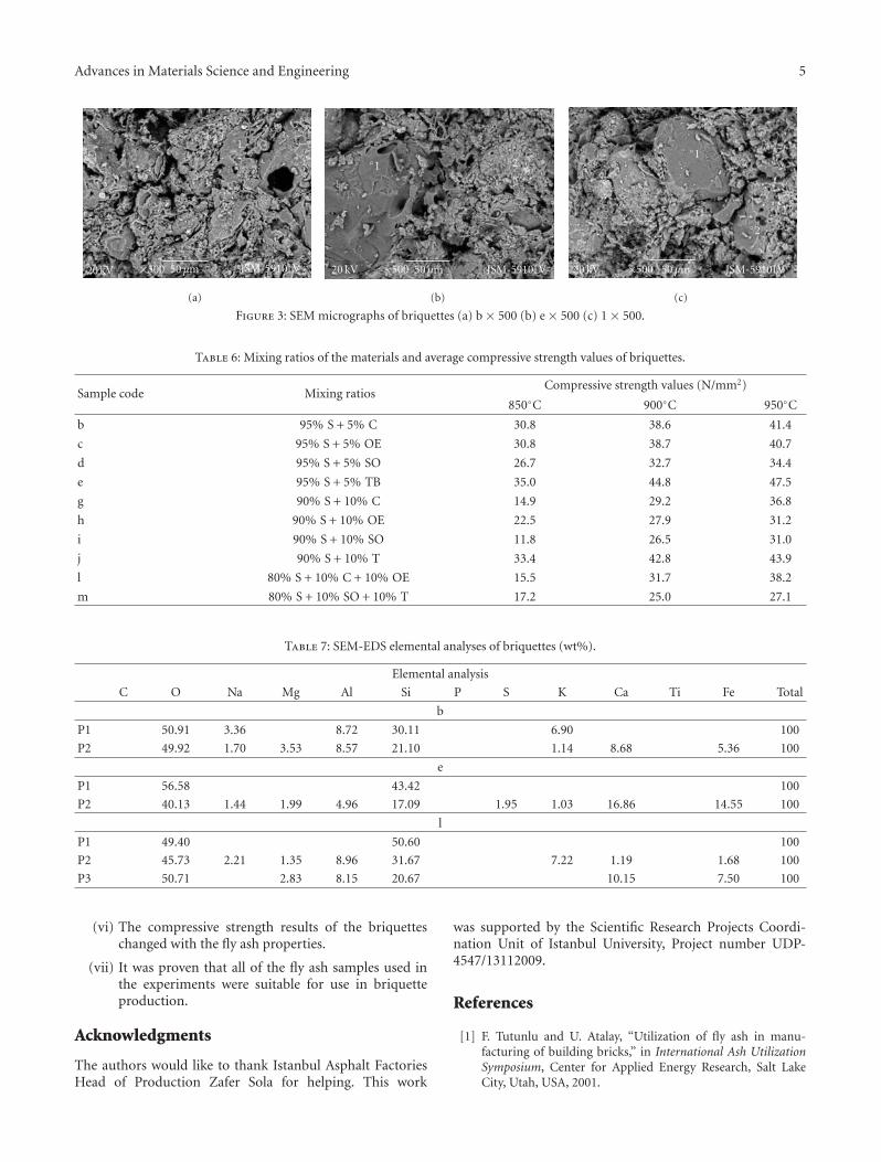
Advances in Materials Science and Engineering 5
◦2 ◦1
20 kV 50 μm×500 JSM-5910LV
(a)
◦2◦1
20 kV 50 μm×500 JSM-5910LV
(b)
◦2
◦1
20 kV 50 μm×500 JSM-5910LV
(c)
Figure 3: SEM micrographs of briquettes (a) b × 500 (b) e × 500 (c) 1 × 500.
Table 6: Mixing ratios of the materials and average compressive strength values of briquettes.
Sample code Mixing ratiosCompressive strength values (N/mm2)
850◦C 900◦C 950◦C
b 95% S + 5% C 30.8 38.6 41.4
c 95% S + 5% OE 30.8 38.7 40.7
d 95% S + 5% SO 26.7 32.7 34.4
e 95% S + 5% TB 35.0 44.8 47.5
g 90% S + 10% C 14.9 29.2 36.8
h 90% S + 10% OE 22.5 27.9 31.2
i 90% S + 10% SO 11.8 26.5 31.0
j 90% S + 10% T 33.4 42.8 43.9
l 80% S + 10% C + 10% OE 15.5 31.7 38.2
m 80% S + 10% SO + 10% T 17.2 25.0 27.1
Table 7: SEM-EDS elemental analyses of briquettes (wt%).
Elemental analysis
C O Na Mg Al Si P S K Ca Ti Fe Total
b
P1 50.91 3.36 8.72 30.11 6.90 100
P2 49.92 1.70 3.53 8.57 21.10 1.14 8.68 5.36 100
e
P1 56.58 43.42 100
P2 40.13 1.44 1.99 4.96 17.09 1.95 1.03 16.86 14.55 100
l
P1 49.40 50.60 100
P2 45.73 2.21 1.35 8.96 31.67 7.22 1.19 1.68 100
P3 50.71 2.83 8.15 20.67 10.15 7.50 100
(vi) The compressive strength results of the briquetteschanged with the fly ash properties.
(vii) It was proven that all of the fly ash samples used inthe experiments were suitable for use in briquetteproduction.
Acknowledgments
The authors would like to thank Istanbul Asphalt FactoriesHead of Production Zafer Sola for helping. This work
was supported by the Scientific Research Projects Coordi-nation Unit of Istanbul University, Project number UDP-4547/13112009.
References
[1] F. Tutunlu and U. Atalay, “Utilization of fly ash in manu-facturing of building bricks,” in International Ash UtilizationSymposium, Center for Applied Energy Research, Salt LakeCity, Utah, USA, 2001.
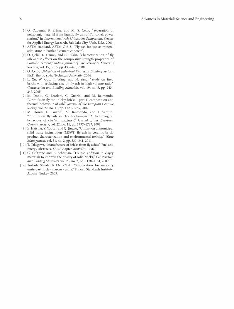
6 Advances in Materials Science and Engineering
[2] O. Ozdemir, B. Erhan, and M. S. Celik, “Separation ofpozzolanic material from lignitic fly ash of Tuncbilek powerstation,” in International Ash Utilization Symposium, Centerfor Applied Energy Research, Salt Lake City, Utah, USA, 2001.
[3] ASTM standard, ASTM C 618, “Fly ash for use as mineraladmixture in Portland cement concrete”.
[4] O. Celik, E. Damcı, and S. Piskin, “Characterization of flyash and it effects on the compressive strength properties ofPortland cement,” Indian Journal of Engineering & MaterialsSciences, vol. 15, no. 5, pp. 433–440, 2008.
[5] O. Celik, Utilization of Industrial Wastes in Building Sectors,Ph.D. thesis, Yıldız Technical University, 2004.
[6] L. Xu, W. Guo, T. Wang, and N. Yang, “Study on firedbricks with replacing clay by fly ash in high volume ratio,”Construction and Building Materials, vol. 19, no. 3, pp. 243–247, 2005.
[7] M. Dondi, G. Ercolani, G. Guarini, and M. Raimondo,“Orimulsion fly ash in clay bricks—part 1: composition andthermal behaviour of ash,” Journal of the European CeramicSociety, vol. 22, no. 11, pp. 1729–1735, 2002.
[8] M. Dondi, G. Guarini, M. Raimondo, and I. Venturi,“Orimulsion fly ash in clay bricks—part 2: technologicalbehaviour of clay/ash mixtures,” Journal of the EuropeanCeramic Society, vol. 22, no. 11, pp. 1737–1747, 2002.
[9] Z. Haiying, Z. Youcai, and Q. Jingyu, “Utilization of municipalsolid waste incineration (MSWI) fly ash in ceramic brick:product characterization and environmental toxicity,” WasteManagement, vol. 31, no. 2, pp. 331–341, 2011.
[10] T. Takegawa, “Manufacture of bricks from fly ashes,” Fuel andEnergy Abstracts, 37-3, Chapter 96/03074, 1996.
[11] G. Cultrone and E. Sebastian, “Fly ash addition in clayeymaterials to improve the quality of solid bricks,” Constructionand Building Materials, vol. 23, no. 2, pp. 1178–1184, 2009.
[12] Turkish Standards EN 771-1, “Specification for masonryunits-part 1: clay masonry units,” Turkish Standards Institute,Ankara, Turkey, 2005.
Hindawi Publishing CorporationAdvances in Materials Science and EngineeringVolume 2011, Article ID 747346, 9 pagesdoi:10.1155/2011/747346
Research Article
Crystallization Behavior and MicrostructuralAnalysis of Strontium Rich (PbxSr1−x)TiO3 GlassCeramics in Presence of La2O3
C. R. Gautam,1 Devendra Kumar,2 and Om Parkash2
1 Department of Physics, University of Lucknow, Lucknow 226007, India2 Department of Ceramic Engineering, Institute of Technology, Banaras Hindu University,Varanasi 221005, India
Correspondence should be addressed to C. R. Gautam, gautam [email protected]
Received 11 April 2011; Accepted 21 June 2011
Academic Editor: Joseph Lai
Copyright © 2011 C. R. Gautam et al. This is an open access article distributed under the Creative Commons Attribution License,which permits unrestricted use, distribution, and reproduction in any medium, provided the original work is properly cited.
Crystallization and microstructural behavior of various strontium-rich glass ceramics in the system 65[(PbxSr1−x)TiO3]-24[2SiO2·B2O3]-5[BaO]-5[K2O]-1[La2O3] (0.0 ≤ x ≤ 0.4) with addition of 1% La2O3 have been investigated. The additionof La2O3 has been found to play an important role in crystallization of perovskite (Pb,Sr)TiO3 as a solid solution phase. Also, itcauses a change in the surface morphology of the fined crystallites of the major phase. Differential thermal analysis (DTA) showsonly one exothermic crystallization peak, which shifts towards higher temperature with increasing amount of strontium oxide.Glasses were subjected to various heat treatment schedules for the crystallization. Very good crystallization of strontium-rich glasscompositions is observed. X-ray diffraction studies confirm that cubic perovskite lead strontium titanate crystallizes as majorphase. Lattice parameter decreases with increasing strontium content similar to lead strontium titanate ceramics. Uniform andinterconnected crystallites are dispersed in glassy matrix.
1. Introduction
Strontium titanate has a cubic structure above −163◦Cwhere it transforms to a paraelectric phase. There is nodielectric anomaly at −163◦C, but a strong elastic anomalyis observed [1]. The dielectric constant follows Curie–Weiss law below room temperature. Strontium titanate is aprototype ceramic with perovskite structure and is of muchtechnological importance. Applications of strontium titanateglass ceramics for a long time have been limited to cryogenictemperature sensors and include a capacitance thermome-ter, a dielectric bolometer, and capacitive energy storagedielectrics [2]. The materials studied by Stookey [3] wereessentially different from the group of glass ceramic materialsdiscovered by King and Stookey [4]. In the later type of mate-rials a relatively unstable glass was devitrified by the additionof a nucleating agent. They found that by dissolving TiO2 insuch a glass a situation could be created in which, in a certaintemperature range, the material was supersaturated in TiO2,giving rise to crystallization of rutile. In some cases, TiO2
did not crystallize as such, but combined with one of themodifying ions of the base glass to precipitate as a titanate,for example, crystallization of SrTiO3 with perovskite struc-ture. The crystallization and microstructural behavior ofglass ceramic with perovskite titanate phases, SrTiO3 [5–14] have been investigated. Thakur et al. [15] investigatedthe crystallization, microstructure and dielectric behavior ofSrTiO3 glass ceramic. SrTiO3 could be crystallized as themajor phase by addition of an appropriate concentration ofK2O and selected heat treatment schedules. In these glassceramics addition of La2O3 enhances the crystallization ofstrontium titanate phase and increases the dielectric constantenormously. Recently Sahu et al. [16] explored the substi-tution of strontium for lead in lead titanate precipitatedin borosilicate glass with suitable choice of compositionand heat treatment schedule. The investigation on thephase development and microstructural characteristics ofthe glass ceramic in the system [SrOTiO2]-[2SiO2B2O3]-[K2O-BaO] showed that the solid solution of SrTiO3 with
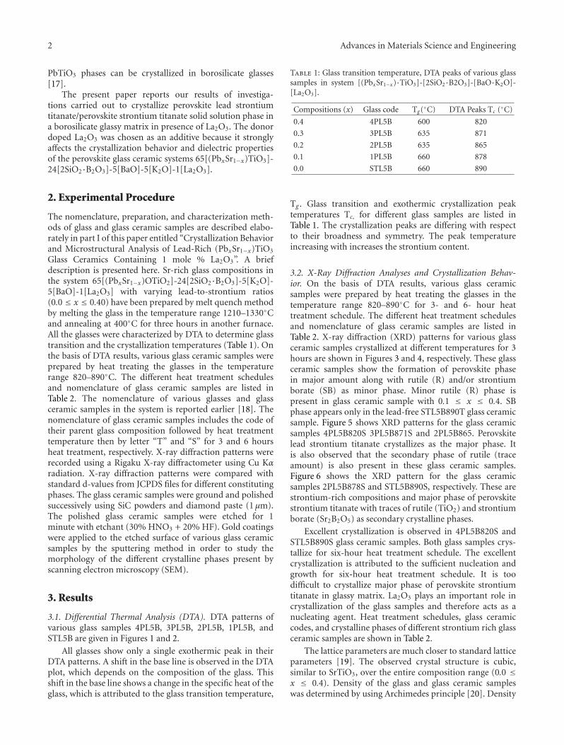
2 Advances in Materials Science and Engineering
PbTiO3 phases can be crystallized in borosilicate glasses[17].
The present paper reports our results of investiga-tions carried out to crystallize perovskite lead strontiumtitanate/perovskite strontium titanate solid solution phase ina borosilicate glassy matrix in presence of La2O3. The donordoped La2O3 was chosen as an additive because it stronglyaffects the crystallization behavior and dielectric propertiesof the perovskite glass ceramic systems 65[(PbxSr1−x)TiO3]-24[2SiO2·B2O3]-5[BaO]-5[K2O]-1[La2O3].
2. Experimental Procedure
The nomenclature, preparation, and characterization meth-ods of glass and glass ceramic samples are described elabo-rately in part I of this paper entitled “Crystallization Behaviorand Microstructural Analysis of Lead-Rich (PbxSr1−x)TiO3
Glass Ceramics Containing 1 mole % La2O3”. A briefdescription is presented here. Sr-rich glass compositions inthe system 65[(PbxSr1−x)OTiO2]-24[2SiO2·B2O3]-5[K2O]-5[BaO]-1[La2O3] with varying lead-to-strontium ratios(0.0 ≤ x ≤ 0.40) have been prepared by melt quench methodby melting the glass in the temperature range 1210–1330◦Cand annealing at 400◦C for three hours in another furnace.All the glasses were characterized by DTA to determine glasstransition and the crystallization temperatures (Table 1). Onthe basis of DTA results, various glass ceramic samples wereprepared by heat treating the glasses in the temperaturerange 820–890◦C. The different heat treatment schedulesand nomenclature of glass ceramic samples are listed inTable 2. The nomenclature of various glasses and glassceramic samples in the system is reported earlier [18]. Thenomenclature of glass ceramic samples includes the code oftheir parent glass composition followed by heat treatmenttemperature then by letter “T” and “S” for 3 and 6 hoursheat treatment, respectively. X-ray diffraction patterns wererecorded using a Rigaku X-ray diffractometer using Cu Kαradiation. X-ray diffraction patterns were compared withstandard d-values from JCPDS files for different constitutingphases. The glass ceramic samples were ground and polishedsuccessively using SiC powders and diamond paste (1 μm).The polished glass ceramic samples were etched for 1minute with etchant (30% HNO3 + 20% HF). Gold coatingswere applied to the etched surface of various glass ceramicsamples by the sputtering method in order to study themorphology of the different crystalline phases present byscanning electron microscopy (SEM).
3. Results
3.1. Differential Thermal Analysis (DTA). DTA patterns ofvarious glass samples 4PL5B, 3PL5B, 2PL5B, 1PL5B, andSTL5B are given in Figures 1 and 2.
All glasses show only a single exothermic peak in theirDTA patterns. A shift in the base line is observed in the DTAplot, which depends on the composition of the glass. Thisshift in the base line shows a change in the specific heat of theglass, which is attributed to the glass transition temperature,
Table 1: Glass transition temperature, DTA peaks of various glasssamples in system [(PbxSr1−x)·TiO3]-[2SiO2·B2O3]-[BaO·K2O]-[La2O3].
Compositions (x) Glass code Tg(◦C) DTA Peaks Tc (◦C)
0.4 4PL5B 600 820
0.3 3PL5B 635 871
0.2 2PL5B 635 865
0.1 1PL5B 660 878
0.0 STL5B 660 890
Tg . Glass transition and exothermic crystallization peaktemperatures Tc, for different glass samples are listed inTable 1. The crystallization peaks are differing with respectto their broadness and symmetry. The peak temperatureincreasing with increases the strontium content.
3.2. X-Ray Diffraction Analyses and Crystallization Behav-ior. On the basis of DTA results, various glass ceramicsamples were prepared by heat treating the glasses in thetemperature range 820–890◦C for 3- and 6- hour heattreatment schedule. The different heat treatment schedulesand nomenclature of glass ceramic samples are listed inTable 2. X-ray diffraction (XRD) patterns for various glassceramic samples crystallized at different temperatures for 3hours are shown in Figures 3 and 4, respectively. These glassceramic samples show the formation of perovskite phasein major amount along with rutile (R) and/or strontiumborate (SB) as minor phase. Minor rutile (R) phase ispresent in glass ceramic sample with 0.1 ≤ x ≤ 0.4. SBphase appears only in the lead-free STL5B890T glass ceramicsample. Figure 5 shows XRD patterns for the glass ceramicsamples 4PL5B820S 3PL5B871S and 2PL5B865. Perovskitelead strontium titanate crystallizes as the major phase. Itis also observed that the secondary phase of rutile (traceamount) is also present in these glass ceramic samples.Figure 6 shows the XRD pattern for the glass ceramicsamples 2PL5B878S and STL5B890S, respectively. These arestrontium-rich compositions and major phase of perovskitestrontium titanate with traces of rutile (TiO2) and strontiumborate (Sr2B2O5) as secondary crystalline phases.
Excellent crystallization is observed in 4PL5B820S andSTL5B890S glass ceramic samples. Both glass samples crys-tallize for six-hour heat treatment schedule. The excellentcrystallization is attributed to the sufficient nucleation andgrowth for six-hour heat treatment schedule. It is toodifficult to crystallize major phase of perovskite strontiumtitanate in glassy matrix. La2O3 plays an important role incrystallization of the glass samples and therefore acts as anucleating agent. Heat treatment schedules, glass ceramiccodes, and crystalline phases of different strontium rich glassceramic samples are shown in Table 2.
The lattice parameters are much closer to standard latticeparameters [19]. The observed crystal structure is cubic,similar to SrTiO3, over the entire composition range (0.0 ≤x ≤ 0.4). Density of the glass and glass ceramic sampleswas determined by using Archimedes principle [20]. Density
Advances in Materials Science and Engineering 3
0 200 400 600 800 1000
Temperature (◦C)
600◦C
820◦Cx = 0.4
ΔT
(a)
635◦C
871◦C
x = 0.3
0 200 400 600 800 1000
Temperature (◦C)
ΔT
(b)
865◦C x = 0.2
635◦C
0 200 400 600 800 1000
Temperature (◦C)
ΔT
(c)
Figure 1: DTA patterns of glasses (a) 4PL5B, x = 0.4, (b) 3PL5B, x = 0.3, and (c) 2PL5B, x = 0.2.
0 200 400 600 800 1000
Temperature (◦C)
660◦C
878◦C
x = 0.1
ΔT
(a)
890◦Cx = 0
0 200 400 600 800 1000
Temperature (◦C)
660◦C
ΔT
(b)
Figure 2: DTA pattern of glasses (a) 1PL5B, x = 0.1, and (b) STL5B, x = 00.
of the glass ceramic samples was determined using distilledwater as the liquid medium.
The following weights were taken and used in the densitycalculations:
W1 is the weight of empty specific gravity bottle (gram);W2 is the weight of specific gravity bottle with sample(gram); W3 is the weight of specific gravity bottle with
sample and distilled water (gram); W4 is the weight ofspecific gravity bottle with distilled water (gram).
Density = W2 −W1
W4 −W1 − (W3 −W2). (1)
3.3. Surface Morphological Analysis. Figures 7(a), 7(b), and7(c) illustrate the scanning electron micrographs for glass
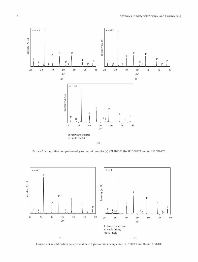
4 Advances in Materials Science and Engineering
20 30 40 50 60 70 80
P
R
P
PP PP
P
PP
x = 0.4
2θ◦
R RP
Inte
nsi
ty(A
.U.)
(a)
PR
20 30 40 50 60 70 80
2θ◦
P
PP
P
P
P
PP
R R
x = 0.3
Inte
nsi
ty(A
.U.)
(b)
20 30 40 50 60 70 80
2θ◦
x = 0.2
P
P
P
P
P
P
P
PP
RR
P: Perovskite titanateR: Rutile (TiO2)
Inte
nsi
ty(A
.U.)
(c)
Figure 3: X-ray diffraction patterns of glass ceramic samples (a) 4PL5B820S (b) 3PL5B871T and (c) 2PL5B865T.
x = 0.1
20 30 40 50 60 70 80
2θ◦
RRP
P
P
PP
P
P
P
Inte
nsi
ty(A
.U.)
(a)
20 30 40 50 60 70 80
2θ◦
x = 0
SB
P
P
P
P
P
P
P RR R
SB: Sr2B2O5
P: Perovskite titanateR: Rutile (TiO2)
Inte
nsi
ty(A
.U.)
(b)
Figure 4: X-ray diffraction patterns of different glass ceramic samples (a) 1PL5B878T and (b) STL5B890T.
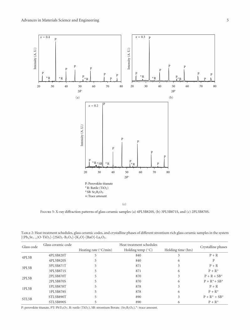
Advances in Materials Science and Engineering 5
20 30 40 50 60 70 80
2θ◦
x = 0.4
∗R
P
P
P
P
P
PP
P∗R ∗R
PInte
nsi
ty(A
.U.)
(a)
20 30 40 50 60 70 80
2θ◦
x = 0.3
∗RP
PP P
P
PP
∗R ∗R
P
P
Inte
nsi
ty(A
.U.)
(b)
∗SB∗R
20 30 40 50 60 70 80
2θ◦
x = 0.2
P
P
P
P
P
P
P
P
P
∗R ∗R
∗:
∗
: Sr2B2O5∗SB
P: Perovskite titanateR: Rutile (TiO2)
Trace amount
Inte
nsi
ty(A
.U.)
(c)
Figure 5: X-ray diffraction patterns of glass ceramic samples (a) 4PL5B820S, (b) 3PL5B871S, and (c) 2PL5B870S.
Table 2: Heat treatment schedules, glass ceramic codes, and crystalline phases of different strontium rich glass ceramic samples in the system[(PbxSr1−x)O·TiO2]-[2SiO2·B2O3]-[K2O]-[BaO]-La2O3.
Glass codeGlass ceramic code Heat treatment schedules
Crystalline phasesHeating rate (◦C/min) Holding temp (◦C) Holding time (hrs)
4PL5B4PL5B820T 5 840 3 P + R
4PL5B820S 5 840 6 P
3PL5B3PL5B871T 5 871 3 P + R
3PL5B871S 5 871 6 P + R∗
2PL5B2PL5B870T 5 870 3 P + R + SB∗
2PL5B870S 5 870 6 P + R∗+ SB∗
1PL5B1PL5B878T 5 878 3 P + R
1PL5B878S 5 878 6 P + R∗
STL5BSTL5B890T 5 890 3 P + R∗ + SB∗
STL5B890S 5 890 6 P + R∗
P: perovskite titanate, PT: PbTi3O7, R: rutile (TiO2), SB: strontium Borate. (Sr2B2O5),∗: trace amount.
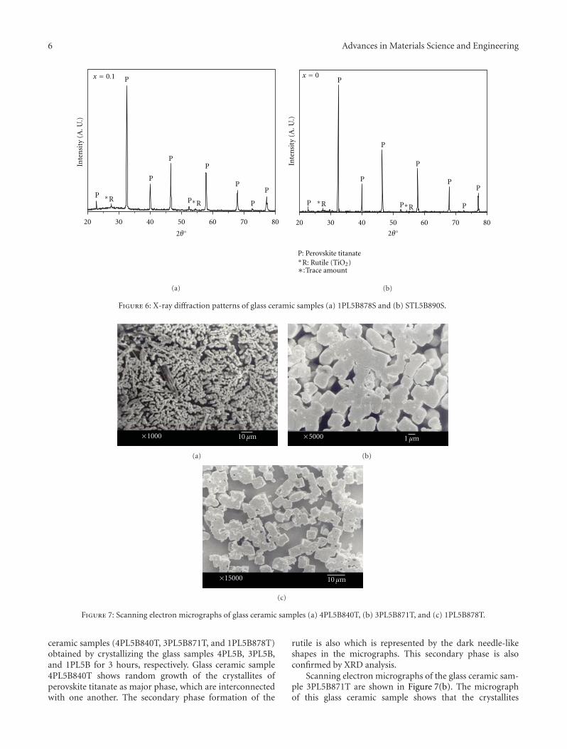
6 Advances in Materials Science and Engineering
20 30 40 50 60 70 80
2θ◦
∗RP
P
P
P
P
P
P
∗R
P
P
x = 0.1In
ten
sity
(A.U
.)
(a)
20 30 40 50 60 70 80
2θ◦
∗RP
P
P
P
P
P
P
∗R
P
P
x = 0
∗:∗P: Perovskite titanate
R: Rutile (TiO2)Trace amount
Inte
nsi
ty(A
.U.)
(b)
Figure 6: X-ray diffraction patterns of glass ceramic samples (a) 1PL5B878S and (b) STL5B890S.
10 μm×1000
(a)
1 μm×5000
(b)
10 μm×15000
(c)
Figure 7: Scanning electron micrographs of glass ceramic samples (a) 4PL5B840T, (b) 3PL5B871T, and (c) 1PL5B878T.
ceramic samples (4PL5B840T, 3PL5B871T, and 1PL5B878T)obtained by crystallizing the glass samples 4PL5B, 3PL5B,and 1PL5B for 3 hours, respectively. Glass ceramic sample4PL5B840T shows random growth of the crystallites ofperovskite titanate as major phase, which are interconnectedwith one another. The secondary phase formation of the
rutile is also which is represented by the dark needle-likeshapes in the micrographs. This secondary phase is alsoconfirmed by XRD analysis.
Scanning electron micrographs of the glass ceramic sam-ple 3PL5B871T are shown in Figure 7(b). The micrographof this glass ceramic sample shows that the crystallites
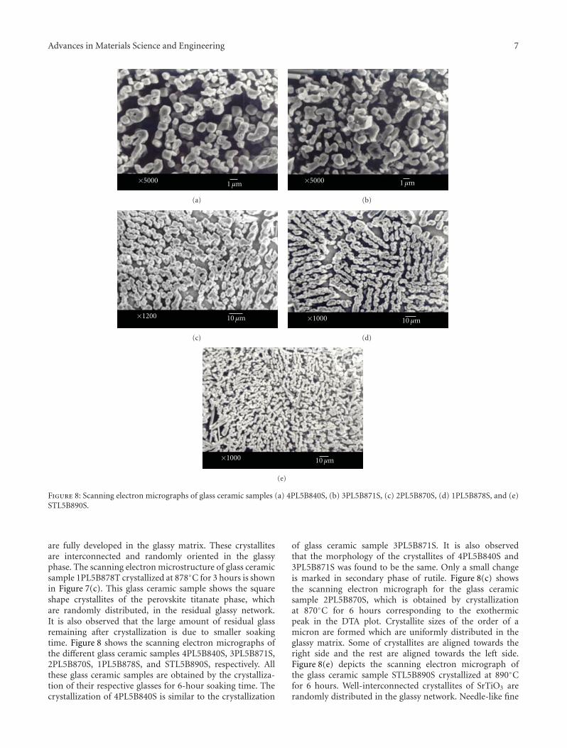
Advances in Materials Science and Engineering 7
1 μm×5000
(a)
1 μm×5000
(b)
10 μm×1200
(c)
10 μm×1000
(d)
10 μm×1000
(e)
Figure 8: Scanning electron micrographs of glass ceramic samples (a) 4PL5B840S, (b) 3PL5B871S, (c) 2PL5B870S, (d) 1PL5B878S, and (e)STL5B890S.
are fully developed in the glassy matrix. These crystallitesare interconnected and randomly oriented in the glassyphase. The scanning electron microstructure of glass ceramicsample 1PL5B878T crystallized at 878◦C for 3 hours is shownin Figure 7(c). This glass ceramic sample shows the squareshape crystallites of the perovskite titanate phase, whichare randomly distributed, in the residual glassy network.It is also observed that the large amount of residual glassremaining after crystallization is due to smaller soakingtime. Figure 8 shows the scanning electron micrographs ofthe different glass ceramic samples 4PL5B840S, 3PL5B871S,2PL5B870S, 1PL5B878S, and STL5B890S, respectively. Allthese glass ceramic samples are obtained by the crystalliza-tion of their respective glasses for 6-hour soaking time. Thecrystallization of 4PL5B840S is similar to the crystallization
of glass ceramic sample 3PL5B871S. It is also observedthat the morphology of the crystallites of 4PL5B840S and3PL5B871S was found to be the same. Only a small changeis marked in secondary phase of rutile. Figure 8(c) showsthe scanning electron micrograph for the glass ceramicsample 2PL5B870S, which is obtained by crystallizationat 870◦C for 6 hours corresponding to the exothermicpeak in the DTA plot. Crystallite sizes of the order of amicron are formed which are uniformly distributed in theglassy matrix. Some of crystallites are aligned towards theright side and the rest are aligned towards the left side.Figure 8(e) depicts the scanning electron micrograph ofthe glass ceramic sample STL5B890S crystallized at 890◦Cfor 6 hours. Well-interconnected crystallites of SrTiO3 arerandomly distributed in the glassy network. Needle-like fine
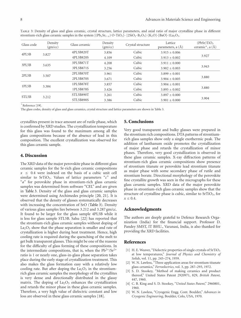
8 Advances in Materials Science and Engineering
Table 3: Density of glass and glass ceramic, crystal structure, lattice parameters, and axial ratio of major crystalline phase in differentstrontium-rich glass ceramic samples in the system [(PbxSr1−x) O·TiO2]- [2SiO2·B2O3]-[K2O]-[BaO]-1La2O3.
Glass code Density(gm/cc)
Glass ceramic Density(gm/cc)
Crystal structure Latticeparameters, a (A)
(PbSr)TiO3
ceramic∗, a (A)
4PL5B 3.8274PL5B820T 3.856 Cubic 3.915± 0.006
3.9274PL5B820S 4.109 Cubic 3.913± 0.002
3PL5B 3.6353PL5B871T 4.208 Cubic 3.911± 0.000
3.9433PL5B871S 3.256 Cubic 3.902± 0.003
2PL5B 3.5072PL5B870T 3.961 Cubic 3.899± 0.001
3.8802PL5B870S 3.671 Cubic 3.904± 0.005
1PL5B 3.3841PL5B878T 3.857 Cubic 3.904± 0.001
3.8801PL5B878S 3.426 Cubic 3.895± 0.002
STL5B 3.212STL5B890T 3.261 Cubic 3.897± 0.000
3.904STL5B890S 3.386 Cubic 3.901± 0.000∗
Reference [19].The glass codes, density of glass and glass ceramics, crystal structure and lattice parameters are shown in Table 3.
crystallites present in trace amount are of rutile phase, whichis confirmed by XRD studies. The crystallization temperaturefor this glass was found to the maximum among all theglass compositions because of the absence of lead in thiscomposition. The excellent crystallization was observed forthis glass ceramic sample.
4. Discussion
The XRD data of the major perovskite phase in different glassceramic samples for the Sr-rich glass ceramic compositionsx ≤ 0.4 were indexed on the basis of a cubic unit cellsimilar to SrTiO3. Values of lattice parameters “c” and“a” for perovskite phase in strontium-rich glass ceramicsamples was determined from software “CEL” and are givenin Table 3. Density of the glass and glass ceramic sampleswere determined using Archimedes principle [20, 21]. It isobserved that the density of glasses systematically decreaseswith increasing the concentration of SrO (Table 3). Densityof various glass samples lies between 3.212 and 3.287 gm/cc.It found to be larger for the glass sample 4PL5B while itis less for glass sample STL5B. Sahu [22] has reported thatthe strontium-rich glass ceramic samples without doping ofLa2O3 show that the phase separation is smaller and rate ofcrystallization is higher during heat treatment. Hence, highcooling rate is required during the quenching of the melt toget bulk transparent glasses. This might be one of the reasonsfor the difficulty of glass forming of these compositions. Inthe intermediate compositions, that is, when the Pb2+/Sr2+
ratio is 1 or nearly one, glass-in-glass phase separation takesplace during the early stage of crystallization treatment. Thisalso makes the glass formation easy with a relatively lowcooling rate. But after doping the La2O3 in the strontium-rich glass ceramic samples the morphology of the crystallitesis very dense and directionally distributed in the glassymatrix. The doping of La2O3 enhances the crystallizationand retards the minor phase in these glass ceramic samples.Therefore, a very high value of dielectric constant and lowloss are observed in these glass ceramic samples [18].
5. Conclusions
Very good transparent and bulky glasses were prepared inthe strontium rich compositions. DTA patterns of strontium-rich glass samples show only a single exothermic peak. Theaddition of lanthanum oxide promotes the crystallizationof major phase and retards the crystallization of minorphases. Therefore, very good crystallization is observed inthese glass ceramic samples. X-ray diffraction patterns ofstrontium-rich glass ceramic compositions show presenceof strontium titanate or perovskite lead strontium titanateas major phase with some secondary phase of rutile andstrontium borate. Directional morphology of the perovskitefine crystallite growth was seen in the micrographs for theseglass ceramic samples. XRD data of the major perovskitephase in strontium-rich glass ceramic samples show that thestructure of crystalline phase is cubic, similar to SrTiO3, forx ≤ 0.4.
Acknowledgments
The authors are deeply grateful to Defence Research Orga-nization (India) for the financial support. Professor D.Pandey SMST, IT BHU., Varanasi, India, is also thanked forproviding the XRD facilities.
References
[1] H. E. Weaver, “Dielectric properties of single crystals of SrTiO3
at low temperatures,” Journal of Physics and Chemistry ofSolids, vol. 11, pp. 245–274, 1959.
[2] W. N. Lawless, “Three application areas for strontium titanateglass-ceramics,” Ferroelectrics, vol. 3, pp. 287–293, 1972.
[3] S. D. Stookey, “Method of making ceramics and productthereof,” United States Patent 2920971, 829, British Patent,447, 1960.
[4] C. B. King and S. D. Stookey, “United States Patent,” 2960801,1960.
[5] W. N. Lawless, “Cryogenic Engg. Cont. Boulder,” Advances inCryogenic Engineering, Boulder, Colo, USA, 1970.
Advances in Materials Science and Engineering 9
[6] W. N. Lawless, “Capacitance thermometry characteristicsof titanate glass-ceramics at low temperature,” Advances inCryogenic Engineering, vol. 16, pp. 261–267, 1971.
[7] W. N. Lawless, “A low temperature glass-ceramic capacitancethermometer,” Review of Scientific Instruments, vol. 42, pp.561–566, 1972.
[8] W. N. Lawless, Private communication, 1981.[9] S. L. Swartz, A. S. Bhalla, L. E. Cross, and W. N. Lawless,
“Strontium titanate (SrTiO3) glass ceramics part I. Crystalliza-tion and microstructure,” Journal of Materials Science, vol. 23,pp. 3997–4003, 1988.
[10] S. L. Swartz, A. S. Bhalla, L. E. Cross, and W. N. Lawless,“SrTiO3 glass ceramics part II. Dielectric properties,” Journalof Materials Science, vol. 23, no. 11, pp. 4004–4012, 1988.
[11] R. K. Mandal, C. Durga Prasad, Om Parkash, and D.Kumar, “Dielectric behaviour of glasses and glass ceramics inthe system BaO-PbO-TiO2-B2O3-SiO2,” Bulletin of MaterialsScience, vol. 9, no. 4, pp. 255–262, 1987.
[12] O. P. Thakur, D. Kumar, Om Parkash, and L. Pandey, “Dielec-tric and microstructural behaviour of strontium titanateborosilicate glass ceramic system,” Bulletin of Materials Science,vol. 18, no. 5, pp. 577–585, 1995.
[13] O. P. Thakur, D. Kumar, and Om Parkash, “Crystallizationmicrostructure development and dielectric behavior of glassceramics in the system [(SrO.TiO2]-[2SiO2.B2O3]-La2O3,”Journal of Materials Science, vol. 37, no. 12, pp. 2597–2606,2002.
[14] S. L. Swartz, E. Breval, and A. S. Bhalla, “Effect of nucleationon the crystallization and dielectric properties of strontiumtitanate glass-ceramics,” The American Ceramic Society Bul-letin, vol. 67, no. 4, pp. 763–770, 1988.
[15] O. P. Thakur, D. Kumar, Om Parkash, and L. Pandey, “Effect ofK2O addition on crystallization and microstructural behaviorof strontium titanate borosilicate glass ceramic system,”Materials Letters, vol. 23, pp. 253–260, 1995.
[16] A. K. Sahu, D. Kumar, and O. Parkash, “Crystallisation of leadstrontium titanate perovskite phase in [(Pb1−xSrx)O.TiO2]-[2SiO2.B2O3]-[K2O] glass ceramics,” The British CeramicTransactions, vol. 102, no. 4, pp. 139–147, 2003.
[17] A. K. Sahu, D. Kumar, O. Parkash, and C. Prakash, “Effectof K2O/BaO ratio on crystallization, microstructure anddielectric properties of strontium titanate borosilicate glassceramics,” Ceramics International, vol. 30, no. 3, pp. 477–483,2004.
[18] D. Kumar, C. R. Gautam, and O. Parkash, “Preparation anddielectric characterization of ferroelectric (PbxSr1-x)TiO3 glassceramics doped with La2O3,” Applied Physics Letters, vol. 89,no. 11, pp. 112908–112911, 2006.
[19] S. Subrahmanyam and E. Goo, “Nucleation of the ferroelectricphase in the (PbxSr1−x)TiO3 system,” Acta Materialia, vol. 46,no. 3, pp. 817–822, 1998.
[20] V. A. Hiremath, S. K. Date, and S. M. Kulkarni, “A newcombustion route to γ-Fe2O3 synthesis,” Bulletin of MaterialsScience, vol. 24, no. 6, pp. 617–621, 2001.
[21] C. R. Gautam, D. Kumar, and Om Parkash, “Dielectricand impedance spectroscopic studies of (Sr1−xPbx)TiO3 glassceramics with addition of Nb2O5,” Bulletin of Material Science.In press.
[22] A. K. Sahu, Preparation microsture and dielectric properties oflead strontium titanate borosilicate glass ceramic system, Ph.D.thesis, Institute of Technology, Banaras Hindu University,India, 2002.
Hindawi Publishing CorporationAdvances in Materials Science and EngineeringVolume 2011, Article ID 402376, 11 pagesdoi:10.1155/2011/402376
Research Article
Crystallization Behavior and MicrostructuralAnalysis of Lead-Rich (PbxSr1−x) TiO3 Glass CeramicsContaining 1 mole % La2O3
C. R. Gautam,1, 2 Devendra Kumar,1, 2 and Om Parkash1, 2
1 Department of Physics, University of Lucknow, Lucknow 226007, India2 Department of Ceramic Engineering, Institute of Technology, Banaras Hindu University, Varanasi 221005, India
Correspondence should be addressed to C. R. Gautam, gautam [email protected]
Received 1 March 2011; Accepted 15 June 2011
Academic Editor: Joseph Lai
Copyright © 2011 C. R. Gautam et al. This is an open access article distributed under the Creative Commons Attribution License,which permits unrestricted use, distribution, and reproduction in any medium, provided the original work is properly cited.
Solid solution of perovskite Pb,SrTiO3 in Pb-rich composition can be crystallized in borosilicate glassy matrix. The addition ofrare earth and transition metal oxides is known to influence the crystallization behavior and surface morphology of perovskitecrystallites in glassy matrix. In the present paper, the glasses in the lead-rich system 64[(PbxSr1−x)·TiO3]-25[2SiO2·B2O3]-5[K2O]-5[BaO] (1 ≤ x ≤ 0.5) with the addition of 1 mol % La2O3 were prepared to study its effect on their crystallization behavior.Differential thermal analysis (DTA) patterns show one or more exothermic crystallization sharp peaks, which shift towardshigher temperature with increasing concentration of SrO. The glasses were subjected to various heat-treatment schedules forcrystallization. X-ray diffraction analysis of these glass ceramic samples shows that major crystalline phase of the entire glassceramic sample with x ≥ 0.5 was found to have tetragonal structure similar to PbTiO3 ceramic, and addition of La2O3 enhancesthe crystallization of the perovskite phase and retards the crystallization of minor phases.
1. Introduction
Glass ceramics are an important class of materials that havebeen commercially quite successful. The pore-free polycrys-talline materials are produced by the controlled crystalliza-tion of glass and composed of randomly oriented crystalswith some residual glass [1]. Crystallization is accomplishedby subjecting the glasses to a carefully regulated heat treat-ment schedule, which results in the nucleation and growth ofcrystal phases within the glass samples [2]. Extensive studieshave been reported on the crystallization and dielectricbehavior of ferroelectric glass ceramics, specifically PbTiO3
and NaNbO3 [3]. These studies show that both the parentglass composition and heat treatment schedule determine thecrystalline phase constitution, microstructure, and dielectricproperties of respective glass ceramics. Bergeron and Russellinvestigated the growth of PbTiO3 from PbO-B2O3-TiO2
glasses and found that the crystallization proceeded mainlyfrom the surface [4]. The crystallization and microstructuralbehavior of glass ceramic with perovskite titanate phases,
such as PbTiO3 [5–11] and SrTiO3 [12–15], have beeninvestigated. Limited work has been carried on the leadstrontium titanate borosilicate glass-ceramic system, despiteits wide applications. Thakur et al. [16] investigated thecrystallization, microstructure, and dielectric behavior ofSrTiO3 glass ceramic with different oxide additions. Theycould crystallize SrTiO3 as a major phase in borosilicate glassceramic system with addition of proper concentration ofalkali oxide K2O and selected heat treatment schedules. Itwas also reported that the addition of La2O3 enhances thecrystallization of strontium titanate [17]. Later on Sahu et al.[18, 19] explored the possibility of substitution of strontiumfor lead in the system [(Pb1−xSrx)O·TiO2]-[2SiO2·B2O3]-[K2O]-[BaO] for crystallization of solid solution perovskitephase. The phase development, microstructural analysis,and dielectric behavior of the glass ceramics indicated thatboth the glass composition and heat-treatment schedulesdetermine the crystalline phase constitution. Solid solutionof PbTiO3 and SrTiO3 phases could be crystallized inborosilicate glasses [20–23].
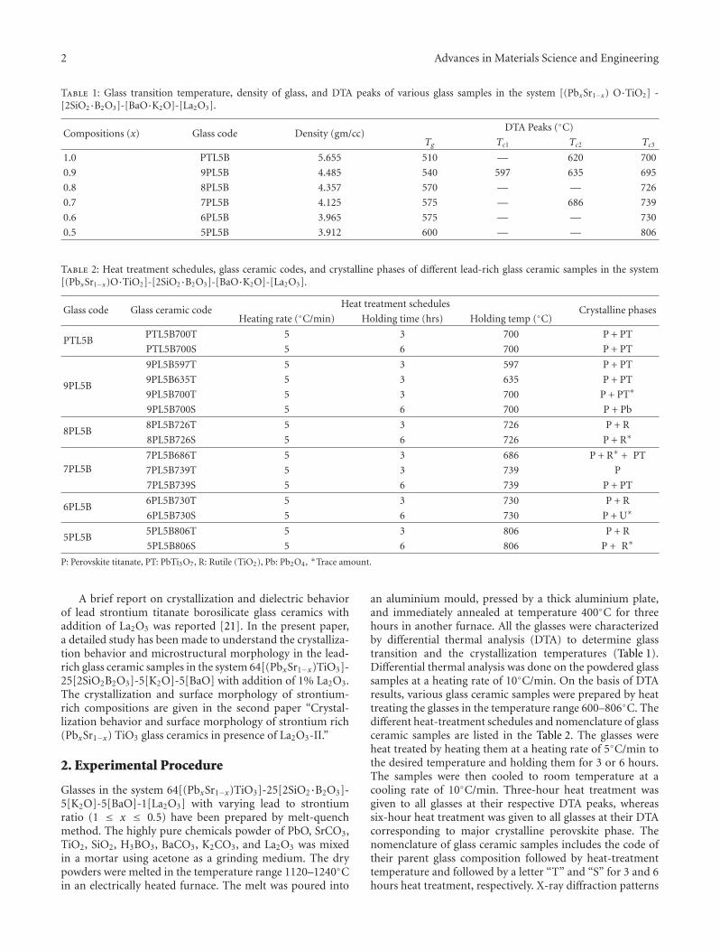
2 Advances in Materials Science and Engineering
Table 1: Glass transition temperature, density of glass, and DTA peaks of various glass samples in the system [(PbxSr1−x) O·TiO2] -[2SiO2·B2O3]-[BaO·K2O]-[La2O3].
Compositions (x) Glass code Density (gm/cc)DTA Peaks (◦C)
Tg Tc1 Tc2 Tc3
1.0 PTL5B 5.655 510 — 620 700
0.9 9PL5B 4.485 540 597 635 695
0.8 8PL5B 4.357 570 — — 726
0.7 7PL5B 4.125 575 — 686 739
0.6 6PL5B 3.965 575 — — 730
0.5 5PL5B 3.912 600 — — 806
Table 2: Heat treatment schedules, glass ceramic codes, and crystalline phases of different lead-rich glass ceramic samples in the system[(PbxSr1−x)O·TiO2]-[2SiO2·B2O3]-[BaO·K2O]-[La2O3].
Glass code Glass ceramic codeHeat treatment schedules
Crystalline phasesHeating rate (◦C/min) Holding time (hrs) Holding temp (◦C)
PTL5BPTL5B700T 5 3 700 P + PT
PTL5B700S 5 6 700 P + PT
9PL5B
9PL5B597T 5 3 597 P + PT
9PL5B635T 5 3 635 P + PT
9PL5B700T 5 3 700 P + PT∗
9PL5B700S 5 6 700 P + Pb
8PL5B8PL5B726T 5 3 726 P + R
8PL5B726S 5 6 726 P + R∗
7PL5B7PL5B686T 5 3 686 P + R∗ + PT
7PL5B739T 5 3 739 P
7PL5B739S 5 6 739 P + PT
6PL5B6PL5B730T 5 3 730 P + R
6PL5B730S 5 6 730 P + U∗
5PL5B5PL5B806T 5 3 806 P + R
5PL5B806S 5 6 806 P + R∗
P: Perovskite titanate, PT: PbTi3O7, R: Rutile (TiO2), Pb: Pb2O4, ∗Trace amount.
A brief report on crystallization and dielectric behaviorof lead strontium titanate borosilicate glass ceramics withaddition of La2O3 was reported [21]. In the present paper,a detailed study has been made to understand the crystalliza-tion behavior and microstructural morphology in the lead-rich glass ceramic samples in the system 64[(PbxSr1−x)TiO3]-25[2SiO2B2O3]-5[K2O]-5[BaO] with addition of 1% La2O3.The crystallization and surface morphology of strontium-rich compositions are given in the second paper “Crystal-lization behavior and surface morphology of strontium rich(PbxSr1−x) TiO3 glass ceramics in presence of La2O3-II.”
2. Experimental Procedure
Glasses in the system 64[(PbxSr1−x)TiO3]-25[2SiO2·B2O3]-5[K2O]-5[BaO]-1[La2O3] with varying lead to strontiumratio (1 ≤ x ≤ 0.5) have been prepared by melt-quenchmethod. The highly pure chemicals powder of PbO, SrCO3,TiO2, SiO2, H3BO3, BaCO3, K2CO3, and La2O3 was mixedin a mortar using acetone as a grinding medium. The drypowders were melted in the temperature range 1120–1240◦Cin an electrically heated furnace. The melt was poured into
an aluminium mould, pressed by a thick aluminium plate,and immediately annealed at temperature 400◦C for threehours in another furnace. All the glasses were characterizedby differential thermal analysis (DTA) to determine glasstransition and the crystallization temperatures (Table 1).Differential thermal analysis was done on the powdered glasssamples at a heating rate of 10◦C/min. On the basis of DTAresults, various glass ceramic samples were prepared by heattreating the glasses in the temperature range 600–806◦C. Thedifferent heat-treatment schedules and nomenclature of glassceramic samples are listed in the Table 2. The glasses wereheat treated by heating them at a heating rate of 5◦C/min tothe desired temperature and holding them for 3 or 6 hours.The samples were then cooled to room temperature at acooling rate of 10◦C/min. Three-hour heat treatment wasgiven to all glasses at their respective DTA peaks, whereassix-hour heat treatment was given to all glasses at their DTAcorresponding to major crystalline perovskite phase. Thenomenclature of glass ceramic samples includes the code oftheir parent glass composition followed by heat-treatmenttemperature and followed by a letter “T” and “S” for 3 and 6hours heat treatment, respectively. X-ray diffraction patterns
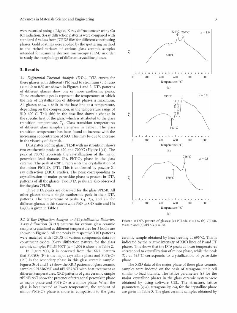
Advances in Materials Science and Engineering 3
were recorded using a Rigaku X-ray diffractometer using CuKα radiation. X-ray diffraction patterns were compared withstandard d-values from JCPDS files for different constitutingphases. Gold coatings were applied by the sputtering methodto the etched surfaces of various glass ceramic samplesintended for scanning electron microscopy (SEM) in orderto study the morphology of different crystalline phases.
3. Results
3.1. Differential Thermal Analysis (DTA). DTA curves forthese glasses with different (Pb) lead to strontium (Sr) ratio(x = 1.0 to 0.5) are shown in Figures 1 and 2. DTA patternsof different glasses show one or more exothermic peaks.These exothermic peaks represent the temperature at whichthe rate of crystallization of different phases is maximum.All glasses show a shift in the base line at a temperature,depending on the composition, in the temperature range of510–600◦C. This shift in the base line shows a change inthe specific heat of the glass, which is attributed to the glasstransition temperature, Tg . Glass transition temperaturesof different glass samples are given in Table 1. The glasstransition temperature has been found to increase with theincreasing concentration of SrO. This may be due to increasein the viscosity of the melt.
DTA pattern of the glass PTL5B with no strontium showstwo exothermic peaks at 620 and 700◦C (Figure 1(a)). Thepeak at 700◦C represents the crystallization of the majorperovskite lead titanate, (P), PbTiO3 phase in the glassceramic. The peak at 620◦C represents the crystallization ofthe minor PbTi3O7 (PT). This is confirmed by powder X-ray diffraction (XRD) studies. The peak corresponding tocrystallization of major perovskite phase is present in DTApatterns of all the glasses. Two DTA peaks are also observedfor the glass 7PL5B.
Three DTA peaks are observed for the glass 9PL5B. Allother glasses show a single exothermic peak in their DTApatterns. The temperature of peaks Tc1, Tc2, and Tc3 fordifferent glasses in this system with PbO to SrO ratio and 1%La2O3 is given in Table 1.
3.2. X-Ray Diffraction Analysis and Crystallization Behavior.X-ray diffraction (XRD) patterns for various glass ceramicsamples crystallized at different temperatures for 3 hours areshown in Figure 3. All the peaks in respective XRD patternswere matched with JCPDS of various compounds data forconstituent oxides. X-ray diffraction pattern for the glassceramic samples PTL5B700T (x = 1.00) is shown in Table 2.
In Figure 3(a), it is observed from the XRD patternthat PbTiO3 (P) is the major crystalline phase and PbTi3O7
(PT) is the secondary phase in this glass ceramic sample.Figures 3(b) and 3(c) show the XRD patterns of glass ceramicsamples 9PL5B695T and 8PL5B726T with heat treatment atdifferent temperatures. XRD patterns of glass ceramic sample9PL5B695T show the presence of tetragonal perovskite phaseas major phase and PbTi3O7 as a minor phase. When theglass is heat treated at lower temperature, the amount ofminor PbTi3O7 phase is more in comparison to the glass
620◦C 700◦C
510◦C
0 200 400 600 800 1000
Temperature (◦C)
ΔT
x = 1.0
(a)
0 200 400 600 800 1000
Temperature (◦C)
695◦C
540◦C
597◦
C63
5◦C
x = 0.9
ΔT
(b)
0 200 400 600 800 1000
Temperature (◦C)
726◦C
570◦C
x = 0.8
ΔT
(c)
Figure 1: DTA pattern of glasses: (a) PTL5B, x = 1.0, (b) 9PL5B,x = 0.9, and (c) 8PL5B, x = 0.8.
ceramic sample obtained by heat treating at 695◦C. This isindicated by the relative intensity of XRD lines of P and PTphases. This shows that the DTA peaks at lower temperaturescorrespond to crystallization of minor phase, while the peakTc3 at 695◦C corresponds to crystallization of perovskitephase.
The XRD data of the major phase of these glass ceramicsamples were indexed on the basis of tetragonal unit cellsimilar to lead titanate. The lattice parameters (s) for themajor crystalline phases in the glass ceramic system wereobtained by using software CEL. The structure, latticeparameters (c, a), tetragonality, c/a, for the crystalline phaseare given in Table 3. The glass ceramic samples obtained by

4 Advances in Materials Science and Engineering
0 200 400 600 800 1000
Temperature (◦C)
686◦C
739◦C
575◦C
x = 0.7
ΔT
(a)
0 200 400 600 800 1000
Temperature (◦C)
730◦C
575◦C
x = 0.6
ΔT
(b)
0 200 400 600 800 1000
Temperature (◦C)
806◦C
600◦C
x = 0.5
ΔT
(c)
Figure 2: DTA pattern of glasses: (a) 7PL5B, x = 0.7, (b) 6PL5B,x = 0.6, and (c) 5PL5B, x = 0.5.
heat-treating glasses with x = 1.0 and 0.9 were found to showsimilar crystallization behavior (Figure 3). They differ onlyin terms of minor phase and value of lattice parameters. XRDpatterns for glass ceramic samples 9PL5B597T; 9PL5B635T;9PL5B695T are shown in Figure 4. The XRD patterns forthese glass ceramic samples show the formation of perovskiteas a major phase. Large amount of PT and small amountof rutile (R) are also present. The amount of secondary
20 30 40 50 60 70 80
2θ0
P
P
P
PP
P
P
PP
P
P
PP P P
PPTPT
PT
Inte
nsi
ty(a
.u.)
x = 1.0
(a)
20 30 40 50 60 70 80
2θ0
P
P
P
P
P
P
P
P
PP
P
P
P PP P PPPT
PT
PT
x = 0.9
Inte
nsi
ty(a
.u.)
(b)
20 30 40 50 60 70 80
2θ0
P
P
P
P
PP
P
P
P
P PP P P PP
PT
R
R
R R R
PbTi3O7
Rutile (TiO2)
x = 0.8
Inte
nsi
ty(a
.u.)
Perovskite titanate
(c)
Figure 3: X-ray diffraction patterns of different glass ceramicsamples: (a) PTL5B700T, (b) 9PL5B695T, and (c) 8PL5B726T.
phase of PbTi3O7 for x = 0.9 obtained by heat treatment athigher temperature is found to be less in comparison to thecomposition with x = 1.0. The glass with x = 0.7 was heattreated for 3 and 6 hours at 686◦C and 739◦C to study theeffect of the crystallization temperature and soaking time onthe microstructure and dielectric behavior of the resultingglass ceramic samples. Perovskite titanate was found to bemajor phase with secondary PbTi3O7 and trace amount of
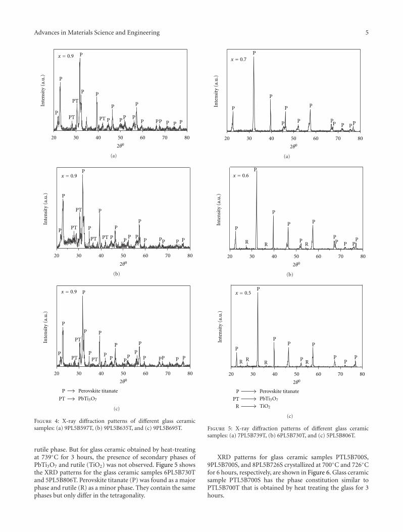
Advances in Materials Science and Engineering 5
20 30 40 50 60 70 80
2θ0
P
P
P
P P
P
P
P P P
P
P PP P P PPTPT
PT
x = 0.9
Inte
nsi
ty(a
.u.)
(a)
20 30 40 50 60 70 80
2θ0
P
P
P
P
P
P
P
PP P
P
P PP P P
PT
PT
PT PT
x = 0.9
Inte
nsi
ty(a
.u.)
(b)
20 30 40 50 60 70 80
2θ0
P
P
P
P
P
P
P
PP
P
PP
P
P
P PP P P
PT
PT
PT
PT
PbTi3O7
x = 0.9
Inte
nsi
ty(a
.u.)
Perovskite titanate
(c)
Figure 4: X-ray diffraction patterns of different glass ceramicsamples: (a) 9PL5B597T, (b) 9PL5B635T, and (c) 9PL5B695T.
rutile phase. But for glass ceramic obtained by heat-treatingat 739◦C for 3 hours, the presence of secondary phases ofPbTi3O7 and rutile (TiO2) was not observed. Figure 5 showsthe XRD patterns for the glass ceramic samples 6PL5B730Tand 5PL5B806T. Perovskite titanate (P) was found as a majorphase and rutile (R) as a minor phase. They contain the samephases but only differ in the tetragonality.
2θ0
20 30 40 50 60 70 80
P
P
P
P
P P
P
PP P PP
x = 0.7
Inte
nsi
ty(a
.u.)
(a)
P
P
P
P
P
PP P P
P
P
R R R
2θ0
20 30 40 50 60 70 80
x = 0.6
Inte
nsi
ty(a
.u.)
(b)
PbTi3O7
P
P
P
PP P
PP
PP
PTTiO2R
R RR R
2θ0
20 30 40 50 60 70 80
x = 0.5
Inte
nsi
ty(a
.u.)
Perovskite titanate
(c)
Figure 5: X-ray diffraction patterns of different glass ceramicsamples: (a) 7PL5B739T, (b) 6PL5B730T, and (c) 5PL5B806T.
XRD patterns for glass ceramic samples PTL5B700S,9PL5B700S, and 8PL5B726S crystallized at 700◦C and 726◦Cfor 6 hours, respectively, are shown in Figure 6. Glass ceramicsample PTL5B700S has the phase constitution similar toPTL5B700T that is obtained by heat treating the glass for 3hours.
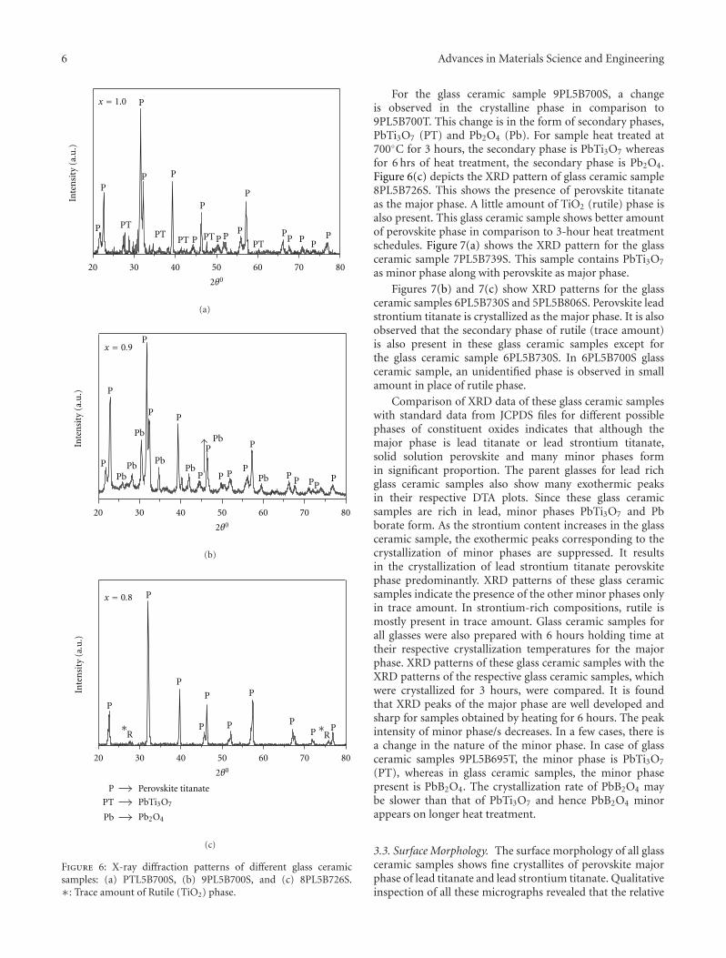
6 Advances in Materials Science and Engineering
P
P
P
P P
P
P
P
PP P P
PPP P
PTPT
PT PTPT
2θ0
20 30 40 50 60 70 80
Inte
nsi
ty(a
.u.)
x = 1.0
(a)
P
PP
P PP
P
P
P
PP PP
P
P
P
2θ0
20 30 40 50 60 70 80
PbPb
Pb
PbPbPb
Pb
x = 0.9
Inte
nsi
ty(a
.u.)
(b)
P
P
P
P
P
P
P
PP P
PbTi3O7
P
PT
R
2θ0
20 30 40 50 60 70 80
Pb2O4Pb
∗R∗
x = 0.8
Inte
nsi
ty(a
.u.)
Perovskite titanate
(c)
Figure 6: X-ray diffraction patterns of different glass ceramicsamples: (a) PTL5B700S, (b) 9PL5B700S, and (c) 8PL5B726S.∗: Trace amount of Rutile (TiO2) phase.
For the glass ceramic sample 9PL5B700S, a changeis observed in the crystalline phase in comparison to9PL5B700T. This change is in the form of secondary phases,PbTi3O7 (PT) and Pb2O4 (Pb). For sample heat treated at700◦C for 3 hours, the secondary phase is PbTi3O7 whereasfor 6 hrs of heat treatment, the secondary phase is Pb2O4.Figure 6(c) depicts the XRD pattern of glass ceramic sample8PL5B726S. This shows the presence of perovskite titanateas the major phase. A little amount of TiO2 (rutile) phase isalso present. This glass ceramic sample shows better amountof perovskite phase in comparison to 3-hour heat treatmentschedules. Figure 7(a) shows the XRD pattern for the glassceramic sample 7PL5B739S. This sample contains PbTi3O7
as minor phase along with perovskite as major phase.
Figures 7(b) and 7(c) show XRD patterns for the glassceramic samples 6PL5B730S and 5PL5B806S. Perovskite leadstrontium titanate is crystallized as the major phase. It is alsoobserved that the secondary phase of rutile (trace amount)is also present in these glass ceramic samples except forthe glass ceramic sample 6PL5B730S. In 6PL5B700S glassceramic sample, an unidentified phase is observed in smallamount in place of rutile phase.
Comparison of XRD data of these glass ceramic sampleswith standard data from JCPDS files for different possiblephases of constituent oxides indicates that although themajor phase is lead titanate or lead strontium titanate,solid solution perovskite and many minor phases formin significant proportion. The parent glasses for lead richglass ceramic samples also show many exothermic peaksin their respective DTA plots. Since these glass ceramicsamples are rich in lead, minor phases PbTi3O7 and Pbborate form. As the strontium content increases in the glassceramic sample, the exothermic peaks corresponding to thecrystallization of minor phases are suppressed. It resultsin the crystallization of lead strontium titanate perovskitephase predominantly. XRD patterns of these glass ceramicsamples indicate the presence of the other minor phases onlyin trace amount. In strontium-rich compositions, rutile ismostly present in trace amount. Glass ceramic samples forall glasses were also prepared with 6 hours holding time attheir respective crystallization temperatures for the majorphase. XRD patterns of these glass ceramic samples with theXRD patterns of the respective glass ceramic samples, whichwere crystallized for 3 hours, were compared. It is foundthat XRD peaks of the major phase are well developed andsharp for samples obtained by heating for 6 hours. The peakintensity of minor phase/s decreases. In a few cases, there isa change in the nature of the minor phase. In case of glassceramic samples 9PL5B695T, the minor phase is PbTi3O7
(PT), whereas in glass ceramic samples, the minor phasepresent is PbB2O4. The crystallization rate of PbB2O4 maybe slower than that of PbTi3O7 and hence PbB2O4 minorappears on longer heat treatment.
3.3. Surface Morphology. The surface morphology of all glassceramic samples shows fine crystallites of perovskite majorphase of lead titanate and lead strontium titanate. Qualitativeinspection of all these micrographs revealed that the relative
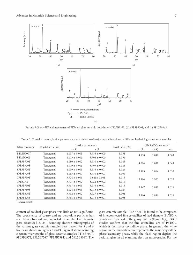
Advances in Materials Science and Engineering 7
x = 0.7
P
P
P
P P
P PP PR
∗R∗PT
∗PT∗
PT∗
2θ0
20 30 40 50 60 70 80
Inte
nsi
ty(a
.u.)
(a)
x = 0.6
PPPPPP
P
PPP
P
P
P
P
P
P
P
2θ0
20 30 40 50 60 70 80
Inte
nsi
ty(a
.u.)
(b)
x = 0.5
PbTi3O7
P
P
P
PP
P P
P
PP P
Rutile (TiO2)R
RR
PT∗
2θ0
20 30 40 50 60 70 80
Inte
nsi
ty(a
.u.)
Perovskite titanate
(c)
Figure 7: X-ray diffraction patterns of different glass ceramic samples: (a) 7PL5B739S, (b) 6PL5B730S, and (c) 5PL5B806S.
Table 3: Crystal structure, lattice parameters, and axial ratio of major crystalline phase in different lead-rich glass ceramic samples.
Glass ceramics Crystal structureLattice parameters
Axial ratio (c/a)(Pb,Sr)TiO3 ceramic∗
c (A) a (A) c (A) a (A) c/a
PTL5B700T Tetragonal 4.117 ± 0.005 3.916 ± 0.005 1.0514.138 3.892 1.063
PTL5B700S Tetragonal 4.125 ± 0.005 3.906 ± 0.005 1.056
9PL5B700T Tetragonal 4.080 ± 0.002 3.910 ± 0.002 1.0434.004 3.837 1.043
9PL5B700S Tetragonal 4.079 ± 0.005 3.909 ± 0.005 1.043
8PL5B726T Tetragonal 4.019 ± 0.001 3.916 ± 0.001 1.0263.983 3.864 1.030
8PL5B726S Tetragonal 4.163 ± 0.007 3.910 ± 0.007 1.064
7PL5B739T Tetragonal 3.974 ± 0.001 3.921± 0.001 1.0133.984 3.903 1.020
7P5B739S Tetragonal 3.977 ± 0.002 3.922 ± 0.002 1.014
6PL5B730T Tetragonal 3.967 ± 0.001 3.916 ± 0.001 1.0133.947 3.882 1.016
6PL5B730S Tetragonal 4.024 ± 0.001 3.915 ± 0.001 1.027
5PL5B806T Tetragonal 3.932 ± 0.002 3.927 ± 0.002 1.0013.960 3.896 1.016
5PL5B806S Tetragonal 3.938 ± 0.001 3.918 ± 0.001 1.005∗
Reference [20].
content of residual glass phase was little or not significant.The coexistence of coarse and ne perovskite particles hasalso been observed and reported in similar lead titanateglass ceramics [18, 24]. Scanning electron micrographs ofthe various glass ceramic samples heat treated for 3 and 6hours are shown in Figures 8 and 9. Figure 8 shows scanningelectron micrographs of glass ceramic samples PTL5B700T,9PL5B695T, 8PL5B726T, 7PL5B739T, and 5PL5B806T. The
glass ceramic sample PTL5B700T is found to be composedof interconnected fine crystallites of lead titanate (PbTiO3),which are dispersed in the glassy matrix (Figure 8(a)). XRDstudies confirm that the fine crystallites are of PbTiO3,which is the major crystalline phase. In general, the whiteregion in the microstructure represents the major crystallinephase/secondary phase, while the black region depicts theresidual glass in all scanning electron micrographs. For the
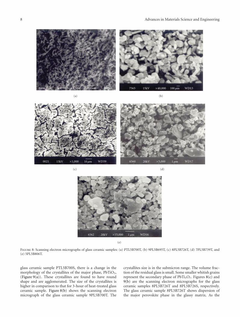
8 Advances in Materials Science and Engineering
0006 ×1,500 WD4815kV 10 μm
(a)
7565 ×40,000 WD1315kV 100 μm
(b)
0021 ×1,000 WD3915kV 10 μm
(c)
6560 ×5,000 WD171 μm20kV
(d)
6562 ×15,000 WD161 μm20kV
(e)
Figure 8: Scanning electron micrographs of glass ceramic samples: (a) PTL5B700T, (b) 9PL5B695T, (c) 8PL5B726T, (d) 7PL5B739T, and(e) 5PL5B806T.
glass ceramic sample PTL5B700S, there is a change in themorphology of the crystallites of the major phase, PbTiO3,(Figure 9(a)). These crystallites are found to have roundshape and are agglomerated. The size of the crystallites ishigher in comparison to that for 3-hour of heat-treated glassceramic sample. Figure 8(b) shows the scanning electronmicrograph of the glass ceramic sample 9PL5B700T. The
crystallites size is in the submicron range. The volume frac-tion of the residual glass is small. Some smaller whitish grainsrepresent the secondary phase of PbTi3O7. Figures 8(c) and9(b) are the scanning electron micrographs for the glassceramic samples 8PL5B726T and 8PL5B726S, respectively.The glass ceramic sample 8PL5B726T shows dispersion ofthe major perovskite phase in the glassy matrix. As the
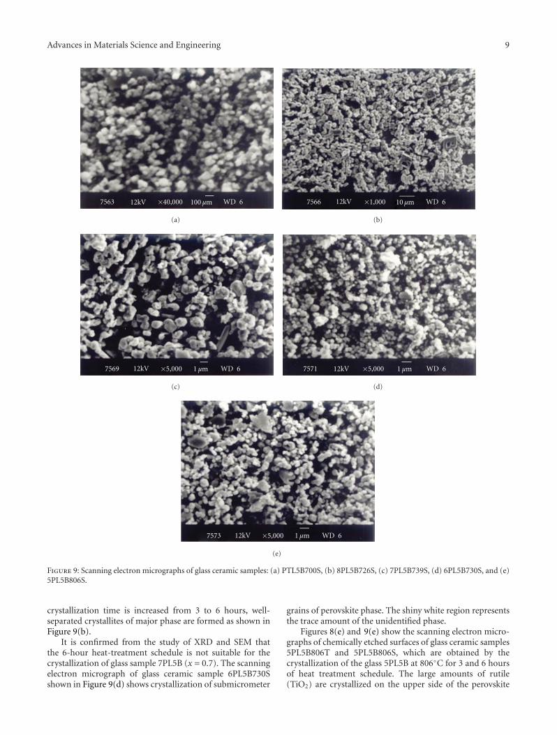
Advances in Materials Science and Engineering 9
×40,000 WD 67563 12kV 100 μm
(a)
×1,000 WD 67566 12kV 10 μm
(b)
×5,000 WD 67569 12kV 1 μm
(c)
×5,000 WD 67571 12kV 1 μm
(d)
×5,000 WD 67573 12kV 1 μm
(e)
Figure 9: Scanning electron micrographs of glass ceramic samples: (a) PTL5B700S, (b) 8PL5B726S, (c) 7PL5B739S, (d) 6PL5B730S, and (e)5PL5B806S.
crystallization time is increased from 3 to 6 hours, well-separated crystallites of major phase are formed as shown inFigure 9(b).
It is confirmed from the study of XRD and SEM thatthe 6-hour heat-treatment schedule is not suitable for thecrystallization of glass sample 7PL5B (x = 0.7). The scanningelectron micrograph of glass ceramic sample 6PL5B730Sshown in Figure 9(d) shows crystallization of submicrometer
grains of perovskite phase. The shiny white region representsthe trace amount of the unidentified phase.
Figures 8(e) and 9(e) show the scanning electron micro-graphs of chemically etched surfaces of glass ceramic samples5PL5B806T and 5PL5B806S, which are obtained by thecrystallization of the glass 5PL5B at 806◦C for 3 and 6 hoursof heat treatment schedule. The large amounts of rutile(TiO2) are crystallized on the upper side of the perovskite
10 Advances in Materials Science and Engineering
titanate major phase, while for the 6-hour heat-treated glassceramic sample 5PL5B806S, the trace amount of rutile isdistributed inside the glassy matrix.
4. Discussion
There is a shift in different XRD peaks positions of majorperovskite phase with changing lead to strontium ratio inthe compositions of the base glasses. The position of XRDpeaks for various glass ceramic samples shifts systematicallywith composition, x or Pb/Sr ratio. The lattice parameters“c” and “a” and the axial ratio (c/a) of the perovskite phasecontinuously decrease as the concentration of SrO increasesin the glass. In general, XRD patterns of the glass ceramicsamples rich in lead with x = 1.0 to 0.5 indicate the formationof tetragonal crystals similar to lead titanate. The shift in theXRD peak positions and hence the resulting changes in thelattice parameters from that of undoped PbTiO3 ceramicscould be due to two factors: (i) formation of PbTiO3 solidsolution with SrTiO3 (ii) and strain due to crystal clamping.Since both of these effects may have been present, the crystalphase developed in these compositions cannot be identifiedunambiguously through room temperature XRD techniques.Some other characterization techniques have to be adoptedto confirm the composition of crystallites.
5. Conclusions
Differential thermal analysis (DTA) patterns show morethan one peak in the lead-rich glass compositions. Thesepeaks are sharp. Doping of La2O3 affects the crystallizationbehavior and dielectric properties of the glass ceramicsamples. The addition of La2O3 promotes the crystallizationof major phase and retards the crystallization of minorphases. X-rays diffraction patterns of lead-rich glass ceramicsamples show that the major phase of PbTiO3 or perovskite(Pb,Sr)TiO3 and a trace amount of pyrochlore phase ofPbTi3O7. Crystalline phase of all the glass ceramic sample ofglasses with x ≤ 0.5 was found to have tetragonal structure.Surface morphology of the fined crystalline phase is observeduniform and well interconnected in residual glassy matrix.
Acknowledgments
The authors are highly grateful to Dr. Chandra Prakashand Dr. O. P. Thakur of the Electroceramic Division, SolidState Physics Laboratory, Delhi (India) for providing accessto the gold coating facility for the glass ceramic samples.Financial support from Defence Research and DevelopmentOrganization (India) is gratefully acknowledged.
References
[1] M. W. Barsoum, Fundamental of Ceramics, McGraw-Hill,Singapore, 1997.
[2] P. W. Mc Millan, Glass Ceramics, Academic Press, London, UK,2nd edition, 1974.
[3] T. Kokubo and M. Tashiro, “Dielectric properties of fine-grained PbTiO3 crystals precipitated in a glass,” Journal ofNon-Crystalline Solids, vol. 13, no. 2, pp. 328–340, 1974.
[4] C. G. Bergeron and C. K. Russell, “Nucleation and growth oflead titanate from a glass,” Journal of the American CeramicSociety, vol. 48, no. 3, pp. 115–118, 1965.
[5] D. G. Grossman and J. O. Isard, “Lead Titanate glass-ceramics,” Journal of the American Ceramic Society, vol. 52, pp.230–241, 1969.
[6] D. G. Grossman and J. O. Isard, “Crystal clamping in PbTiO3
glass-ceramics,” Journal of Materials Science, vol. 4, no. 12, pp.1059–1063, 1969.
[7] S. M. Lynch and J. E. Shelby, “Crystal clamping in lead titanateglass-ceramics,” Journal of the American Ceramic Society, vol.67, no. 6, pp. 424–427, 1984.
[8] W. Mianxue and Z. Peinan, “Piezoelectricity, pyroelectricityand ferroelectricity in glass ceramics based on PbTiO3,”Journal of Non-Crystalline Solids, vol. 84, no. 1–3, pp. 344–351,1986.
[9] J. J. Shyu and Y. S. Yang, “Crystallization of a PbO-BaO-TiO2-Al2O3-SiO2 glass,” Journal of the American Ceramic Society, vol.78, no. 6, pp. 1463–1468, 1995.
[10] W. N. Lawless, “Thermometer equations for low-temperatureglass-ceramic capacitance thermometers,” Cryogenics, vol. 42,pp. 561–566, 1972.
[11] W. N. Lawless, “Three application areas for strontium titanateglass-ceramics,” Ferroelectrics, vol. 3, pp. 287–293, 1971.
[12] W. N. Lawless, “Some low-temperature properties and appli-cations of SrTiO3 crystallized from glass,” Ferroelectrics, vol. 7,pp. 379–381, 1974.
[13] S. L. Swartz, E. Breval, and A. S. Bhalla, “Effect of nucleationon the crystallization and dielectric properties of strontiumtitanate glass-ceramics ,” American Ceramic Society Bulletin,vol. 67, no. 4, pp. 763–770, 1988.
[14] S. L. Swartz, E. Breval, C. A. Randall, and B. H. Fox, “Stron-tium Titanate (SrTiO3) glass ceramics—part I: crystallizationand Microstructure,” Journal of Materials Science, vol. 23, no.11, pp. 3997–4003, 1988.
[15] S. L. Swartz, A. S. Bhalla, L. E. Cross, and W. N. Lawless,“Strontium Titanate (SrTiO3) glass ceramics—part II: dielec-tric properties,” Journal of Materials Science, vol. 23, pp. 4004–4012, 1988.
[16] O. P. Thakur, D. Kumar, O. Parkash, and L. Pandey, “Effect ofK2O adiition on crystallization and microstructural behaviorof strontium Titanate borosilicate glass ceramic system,”Journal of Materials Letters, vol. 23, pp. 253–260, 1995.
[17] O. P. Thakur, Crystallization, microstructure and dielectricbehavior of strontium Titanate borosilicate glass ceramics withsome additives, Ph.D. thesis, Banaras Hindu University,Varanasi, India, 1998.
[18] A. K. Sahu, D. Kumar, and O. Parkash, “Crystallisation of leadstrontium titanate perovskite phase in [(Pb1−xSrx)O·TiO2]–[2SiO2·B2O3]–[K2O] glass ceramics,” British Ceramic Trans-actions, vol. 102, no. 4, pp. 139–147, 2003.
[19] A. K. Sahu, D. Kumar, and O. Parkash, “Lead-strontiumtitanate glass ceramics: I—crystallization and microstructure,”Journal of Materials Science, vol. 41, no. 7, pp. 2075–2085,2006.
[20] S. Subrahmanyam and E. Goo, “Nucleation of the ferroelectricphase in the (PbxSr1−x)TiO3 system,” Acta Materialia, vol. 46,no. 3, pp. 817–822, 1998.
[21] A. K. Sahu, D. Kumar, O. Parkash, O. P. Thakur, and C.Prakash, “Effect of K2O/BaO ratio on crystallization, micro-structure and dielectric properties of strontium titanateborosilicate glass ceramics,” Ceramics International, vol. 30,no. 3, pp. 477–483, 2004.
Advances in Materials Science and Engineering 11
[22] D. Kumar, C. R. Gautam, and O. Parkash, “Preparationand dielectric characterization of ferroelectric (PbxSr1−x)TiO3
glass ceramics doped with La2O3,” Applied Physics Letters, vol.89, no. 11, pp. 112908–112910, 2006.
[23] W. Liu, C. H. Mao, G. X. Dong, and J. Du, “Effects of PbOand SrO contents on crystallization and dielectric proper-ties of PbO–SrO–Na2O–Nb2O5–SiO2 glass-ceramics system,”Ceramics International, vol. 35, no. 3, pp. 1261–1265, 2009.
[24] A. Bahramia, Z. Ali Nematia, P. Alizadehb, and M.Bolandia, “Crystallization and electrical properties of[(Pb1−xSrx)·TiO3]-[(2SiO2·B2O3)]-[K2O]glass–ceramics,”Journal of Materials Processing Technology, vol. 206, pp.126–131, 2008.
Hindawi Publishing CorporationAdvances in Materials Science and EngineeringVolume 2011, Article ID 768143, 6 pagesdoi:10.1155/2011/768143
Research Article
Powder Characterization and Electrochemical Properties ofLiNi0.5Mn1.5O4 Cathode Materials Produced by Large SprayPyrolysis Using Flame Combustion
Shinsuke Akao, Motofumi Yamada, Takayuki Kodera, Kenichi Myoujin, and Takashi Ogihara
Graduate School of Fiber Amenity Engineering, University of Fukui, 9-1 Bunkyo 3, Fukui-shi, Fukui 910-8507, Japan
Correspondence should be addressed to Takashi Ogihara, [email protected]
Received 2 April 2011; Accepted 7 June 2011
Academic Editor: Joseph Lai
Copyright © 2011 Shinsuke Akao et al. This is an open access article distributed under the Creative Commons Attribution License,which permits unrestricted use, distribution, and reproduction in any medium, provided the original work is properly cited.
LiNi0.5Mn1.5O4 cathode materials were produced by spray pyrolysis apparatus using the flame combustion. SEM revealed that as-prepared powders had spherical morphology with porous microstructure which had an average diameter of about 2 μm with broadsize distribution. After the calcination, LiNi0.5Mn1.5O4 powders with polygonal morphology and narrow particle size distributionwere obtained. XRD showed that LiNi0.5Mn1.5O4 was well crystallized after the calcination at 900◦C. Rechargeable measurementof LiNi0.5Mn1.5O4 cathode showed that the long plateau was observed at 4.7 V in discharge curve of LiNi0.5Mn1.5O4 cathode and itsdischarge capacity was 145 mAh/g at 1 C. The capacity retention of LiNi0.5Mn1.5O4 cathode were 95% at 1 C after 100 cycles. Thedischarge capacity and capacity retention of LiNi0.5Mn1.5O4 cathode were 125 mAh/g and 88% at 20 C. LiNi0.5Mn1.5O4 cathodeexhibited also stable cycle performance at 50◦C.
1. Introduction
Lithium ion batteries have been extensively used as energystorage devices for portable electronics. Recently, these arewell noted as the power sources for the vehicles such asEV and HEV [1]. Both layered type LiCoO2 and spineltype LiMn2O4 is the most important cathode materialsbecause of their high operating voltage at 4 V [2, 3]. LiCoO2
have been mostly used as cathode material of commerciallithium ion batteries. However, LiCoO2 has a problem relatedto capacity fading due to the instability in rechargeablecycles. Cobalt is also expensive and its resource is notsufficient. Furthermore, the thermal stability is very lowin the rechargeable process. Therefore, LiCoO2 cathodematerial is not suitable as a lithium ion battery for EVand HEV. On the other hand, LiMn2O4 cathode material issuitable due to their advantages such as low cost, abundance,nontoxicity, and thermally stable [4]. It was known that Ni-substitute lithium manganese oxide spinel (LiNi0.5Mn1.5O4)was exhibited rechargeable behavior at about 5 V [5–7].
LiNi0.5Mn1.5O4 has attracted significant attention asa cathode material with high energy density. It was important
to control the chemical composition to obtain homogeneousLiNi0.5Mn1.5O4 powders. So far, LiNi0.5Mn1.5O4 powdershave been prepared via the solution techniques such as copre-cipitation [8, 9], spray drying [10], sol-gel [11, 12], polymergel [13] and chemical wet process [14]. LiNi0.5Mn1.5O4
powders have been also prepared via the improved solid statereaction [15–18] and molten salt reaction [19, 20].
We have noted spray pyrolysis in order to preparea homogeneous LiNi0.5Mn1.5O4 powder. It was well knownthat the spray pyrolysis was an effective process for the rapidsynthesis of homogeneous multicomponent oxide powders[21]. We have tried to synthesize various type cathodematerials for lithium ion battery by spray pyrolysis [22–24].The rechargeable capacity and cycle performance of lithiumion battery were improved by using the cathode materials forlithium ion battery derived from spray pyrolysis. Park andSun [25] have reported that homogeneous LiNi0.5Mn1.5O4
powders can be obtained by ultrasonic spray pyrolysis. How-ever, spray pyrolysis has not been applied as an industrialprocess because it is difficult to homogeneously pyrolyzethe mist of inorganic salts in the electrical furnace that thescale-up was done. The difference of pyrolysis temperature
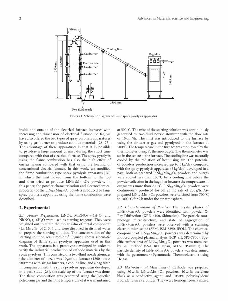
2 Advances in Materials Science and Engineering
2500
mm
1800
mm
580 mm
1995
mm
Bag filter
Cooling line
Gas burner
Thermometer
2500 mm
Gas burner
Gas burner
Two-fluid nozzle
Figure 1: Schematic diagram of flame spray pyrolysis apparatus.
inside and outside of the electrical furnace increases withincreasing the dimension of electrical furnace. So far, wehave also offered the two types of spray pyrolysis apparatusesby using gas burner to produce cathode materials [26, 27].The advantage of these apparatuses is that it is possibleto pyrolyze a large amount of mist during the short timecompared with that of electrical furnace. The spray pyrolysisusing the flame combustion has also the high effect ofenergy saving compared with that using the heating ofconventional electric furnace. In this work, we modifiedthe flame combustion type spray pyrolysis apparatus [26]in which the mist flowed from the bottom to the topand then tried to produce LiNi0.5Mn1.5O4 powders. Inthis paper, the powder characterization and electrochemicalproperties of the LiNi0.5Mn1.5O4 powders produced by largespray pyrolysis apparatus using the flame combustion weredescribed.
2. Experimental
2.1. Powder Preparation. LiNO3, Mn(NO3)2·6H2O, andNi(NO3)2·6H2O were used as starting reagents. They wereweighted out to attain the molar ratio of metal component(Li : Mn : Ni) of 2 : 3 : 1 and were dissolved in distilled waterto prepare the starting solution. The concentration of thestarting solution was 1 mol/dm3. Figure 1 shows schematicdiagram of flame spray pyrolysis apparatus used in thiswork. The apparatus is a prototype developed in order toverify the industrial production of cathode materials by thespray pyrolysis. This consisted of a two-fluid nozzle atomizer(the diameter of nozzle was 10 μm), a furnace (1800 mm ×580 mm) with six gas burners, a cooling line, and a bag filter.In comparison with the spray pyrolysis apparatus developedin a past study [26], the scale-up of the furnace was done.The flame combustion was generated using the liquefiedpetroleum gas and then the temperature of it was maintained
at 500◦C. The mist of the starting solution was continuouslygenerated by two-fluid nozzle atomizer with the flow rateof 10 dm3/h. The mist was introduced to the furnace byusing the air carrier gas and pyrolyzed in the furnace at500◦C. The temperature in the furnace was monitored by thethermometer using Pt thermocouple. The thermometer wasset in the centre of the furnace. The cooling line was naturallycooled by the radiation of heat using air. The potentialof powders production increased up to 5 kg/day comparedwith the spray pyrolysis apparatus (3 kg/day) developed in apast. Both as-prepared LiNi0.5Mn1.5O4 powders and outgaswere cooled less than 100◦C by a cooling line before thepowder collection in the bag filter because the temperature ofoutgas was more than 200◦C. LiNi0.5Mn1.5O4 powders werecontinuously produced for 5 h at the rate of 200 g/h. As-prepared LiNi0.5Mn1.5O4 powders were calcined from 700◦Cto 1000◦C for 2 h under the air atmosphere.
2.2. Characterization of Powders. The crystal phases ofLiNi0.5Mn1.5O4 powders were identified with powder X-Ray Diffraction (XRD-6100, Shimadzu). The particle mor-phology, microstructure, and state of aggregation ofLiNi0.5Mn1.5O4 powders were observed with a scanningelectron microscope (SEM, JSM-6390, JEOL). The chemicalcomponent of LiNi0.5Mn1.5O4 powders was determined byinduced coupled plasma analysis (ICP, SII, SPS-7800). Spe-cific surface area of LiNi0.5Mn1.5O4 powders was measuredby BET method (SSA, BEL Japan, BELSORP-miniII). Theparticle density of LiNi0.5Mn1.5O4 powders was determinedwith the pycnometer (Pycnomatic, Thermoelectron) usingHe gas.
2.3. Electrochemical Measurement. Cathode was preparedusing 80 wt% LiNi0.5Mn1.5O4 powders, 10 wt% acetyleneblack as a conductive agent, and 10 wt% polyvinylidenefluoride resin as a binder. They were homogeneously mixed
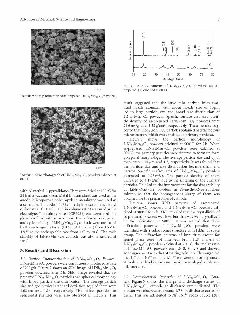
Advances in Materials Science and Engineering 3
10 μm
Figure 2: SEM photograph of as-prepared LiNi0.5Mn1.5O4 powders.
10 μm
Figure 3: SEM photograph of LiNi0.5Mn1.5O4 powders calcined at800◦C.
with N-methyl-2-pyrrolidone. They were dried at 120◦C for24 h in a vacuum oven. Metal lithium sheet was used as theanode. Microporous polypropylene membrane was used asa separator. 1 mol/dm3 LiPF6 in ethylene carbonate/diethylcarbonate (EC : DEC = 1 : 1 in volume ratio) was used as theelectrolyte. The coin type cell (CR2032) was assembled in aglove box filled with an argon gas. The rechargeable capacityand cycle stability of LiNi0.5Mn1.5O4 cathode were measuredby the rechargeable tester (BTS2004H, Hosen) from 3.5 V to4.9 V at the rechargeable rate from 1 C to 20 C. The cyclestability of LiNi0.5Mn1.5O4 cathode was also measured at50◦C.
3. Results and Discussion
3.1. Particle Characterization of LiNi0.5Mn1.5O4 Powders.LiNi0.5Mn1.5O4 powders were continuously produced at rateof 200 g/h. Figure 2 shows an SEM image of LiNi0.5Mn1.5O4
powders obtained after 5 h. SEM image revealed that as-prepared LiNi0.5Mn1.5O4 particles had spherical morphologywith broad particle size distribution. The average particlesize and geometrical standard deviation (σg) of them were1.68 μm and 1.34, respectively. The follow particles orspheroidal particles were also observed in Figure 2. This
10 20 30 40 50 60 70 80
Inte
nsi
ty(a
.u.)
2θ (deg) (CuK)
(b)
(a)
(111
)
(311
)(2
22) (4
00)
(331
)
(511
)
(440
)(5
31)
(533
)(6
22)
Figure 4: XRD patterns of LiNi0.5Mn1.5O4 powders, (a) as-prepared, (b) calcined at 800◦C.
result suggested that the large mist derived from two-fluid nozzle atomizer with about nozzle size of 10 μmled to large particle size and broad size distribution ofLiNi0.5Mn1.5O4 powders. Specific surface area and parti-cle density of as-prepared LiNi0.5Mn1.5O4 powders were24.6 m2/g and 3.32 g/cm3, respectively. These results sug-gested that LiNi0.5Mn1.5O4 particles obtained had the porousmicrostructure which was consisted of primary particles.
Figure 3 shows the particle morphology ofLiNi0.5Mn1.5O4 powders calcined at 900◦C for 2 h. Whenas-prepared LiNi0.5Mn1.5O4 powders were calcined at900◦C, the primary particles were sintered to form uniformpolygonal morphology. The average particle size and σg ofthem were 1.01 μm and 1.3, respectively. It was found thatthe particle size and size distribution became small andnarrow. Specific surface area of LiNi0.5Mn1.5O4 powdersdecreased to 1.03 m2/g. The particle density of themincreased to 4.17 g/m3 due to the sintering of the primaryparticles. This led to the improvement for the dispersibilityof LiNi0.5Mn1.5O4 powders in N-methyl-2-pyrrolidonesolvent, so that the homogeneous slurry of them wasobtained for the preparation of cathode.
Figure 4 shows XRD patterns of as-preparedLiNi0.5Mn1.5O4 powders and LiNi0.5Mn1.5O4 powders cal-cined at 900◦C for 2 h. XRD revealed that the crystallinity ofas-prepared powders was low, but that was well crystallizedby the calcination at 900◦C. It was seemed that thesediffraction patterns of LiNi0.5Mn1.5O4 powders wereidentified with a cubic spinel structure with Fd3m of spacegroup. The diffraction patterns of impurities except forspinel phase were not observed. From ICP analysis ofLiNi0.5Mn1.5O4 powders calcined at 900◦C, the molar ratioof LiNi0.5Mn1.5O4 powders was 1.0 : 0.49 : 1.49 and showedgood agreement with that of starting solution. This suggestedthat Li+ ion, Ni2+ ion and Mn4+ ion were uniformly mixedat molecular level in each mist which was played a role as amicroreactor.
3.2. Electrochemical Properties of LiNi0.5Mn1.5O4 Cath-ode. Figure 5 shows the charge and discharge curves ofLiNi0.5Mn1.5O4 cathode at discharge rate indicated. Theplateau was observed at around 4.7 V in discharge curves ofthem. This was attributed to Ni2+/Ni4+ redox couple [28].
4 Advances in Materials Science and Engineering
Capacity (mAh·g−1)0 30 60 90 120 150 180
2
3
4
5
6
Vol
tage
(V)
(d)(c) (b)(a)
Rate
(a) 1 C(b) 3 C
(c) 10 C(d) 20 C
Figure 5: Discharge curves of LiNi0.5Mn1.5O4 cathode at rateindicated.
0 5 10 15 20 250
20
40
60
80
100
Eci
ency
(%)
Discharge rate (C)
Figure 6: Discharge efficiency of LiNi0.5Mn1.5O4 cathode at rateindicated.
The discharge capacity of LiNi0.5Mn1.5O4 cathode was145 mAh/g at 1 C. Another plateau was observed at around4 V in the discharge curve of LiNi0.5Mn1.5O4 cathode at1 C. This was attributed to Mn3+/Mn4+ redox couple.The discharge capacity decreased with increasing the dis-charge rate. The plateau at 4 V disappeared at more than10 C. The discharge capacity of LiNi0.5Mn1.5O4cathode was125 mAh/g when the discharge rate was 20 C. The voltageof LiNi0.5Mn1.5O4 cathode also lowered about 0.1 V at 20 C.The disappearance of plateau and the decrease of voltage mayresult in the increase in the polarization of cell. This wasreported in the literature [29].
Figure 6 shows the discharge efficiency of LiNi0.5Mn1.5O4
cathode at the rate indicated. The discharge efficiency ofLiNi0.5Mn1.5O4 cathode was 95% at 1 C. Although, thedischarge efficiency of LiNi0.5Mn1.5O4 cathode decreasedwith increasing the discharge rate, it kept more than 85% ateven 20 C. It is considered that LiNi0.5Mn1.5O4 particles with
0 20 40 60 80 1000
50
100
150
200
1 C
5 C
10 C
20 C
Dis
char
geca
paci
ty(m
Ah·g−1
)
Cycle number (n)
Figure 7: Relation between discharge capacity and cycle number atrate indicated.
0 20 40 60 80 1000
50
100
150
200
1 C
10 C 10 C
1 C 1 C
Dis
char
geca
paci
ty(m
Ah·g−1
)
Cycle number (n)
Figure 8: The change of a discharge capacity in alternately repeatingrechargeable to 20 times at 1 C and 10 C.
uniform polygonal morphology and high crystallinity areresponsible of these outstanding rechargeable performances.
Figure 7 shows the relation between discharge capacityand cycle number of LiNi0.5Mn1.5O4 cathode at the dischargerate indicated. The rechargeable test was carried out up to100 cycles at room temperature. The capacity fading wasslightly observed in LiNi0.5Mn1.5O4 cathode at 1 C after 100cycles. The capacity retention of LiNi0.5Mn1.5O4 cathodewas 95% at 1 C. That of LiNi0.5Mn1.5O4 cathode obtaineddecreased with increasing the discharge rate and then capac-ity fading increased. The cycle retention of LiNi0.5Mn1.5O4
cathode was 88% at 20 C after 100 cycles. It was foundthat LiNi0.5Mn1.5O4 cathode had excellent the cycle stability.It was considered that the rechargeable reaction uniformlyoccurred at the level of interface between particle andelectrolyte because of narrow particle size distribution.
Figure 8 shows the cycle performance of LiNi0.5Mn1.5O4
when the cycle test was done alternately for 10 cycles at 1 C
Advances in Materials Science and Engineering 5
0
50
100
150
200
0 50 100 150 200
30 ◦C
50 ◦C
Dis
char
geca
paci
ty(m
Ah·g−1
)
Cycle number (n)
Figure 9: Relation between discharge capacity and cycle number at30◦C and 50◦C.
and 10 C. 140 mAh/g of discharge capacity was maintainedat 1 C. The discharge capacity of LiNi0.5Mn1.5O4 cathodedecreased to 130 mAh/g at 10 C. LiNi0.5Mn1.5O4 cathode hadalso good stability for the alternate cycle test at the higherand lower dischargeable rate. This suggested that the spinelstructure of LiNi0.5Mn1.5O4 was also stable for intercalationof Li+ ion at the high and low rechargeable rate. Thissuggests that LiNi0.5Mn1.5O4 spinel structure may lead to thehigh cycle stability for the volume change during the rapidintercalation of lithium ion.
Figure 9 shows the cycle performance of LiNi0.5Mn1.5O4
cathode at 30◦C and 50◦C. The cycle test was examined at1 C for 200 cycles. The discharge capacity of LiNi0.5Mn1.5O4
cathode at 30◦C was 135 mAh/g after 200 cycles. Thecapacity retention of it was 95%. The discharge capacity ofLiNi0.5Mn1.5O4 cathode at 50◦C was 115 mAh/g after 200cycles. The capacity retention of it was 91%. It was foundthat the cycle performance at 50◦C was also stable as well asthat at room temperature.
4. Conclusions
LiNi0.5Mn1.5O4 cathode materials were successfully pro-duced by spray pyrolysis apparatus using the flame com-bustion. As-prepared LiNi0.5Mn1.5O4 powders had sphericalmorphology with porous microstructure which had anaverage diameter of 1.68 μm with broad size distribution.After the calcination, LiNi0.5Mn1.5O4 powders with polygo-nal morphology and narrow particle size distribution wereobtained. LiNi0.5Mn1.5O4 powders were well crystallized afterthe calcination at 900◦C and the chemical composition wasin good agreement with that of starting solution. Recharge-able measurement of LiNi0.5Mn1.5O4 cathode showed thatthe plateau was observed at 4.7 V in discharge curve ofLiNi0.5Mn1.5O4 cathode and its discharge capacity was146 mAh/g at 1 C. The capacity retention of LiNi0.5Mn1.5O4
cathode was 95% at 1 C after 100 cycles. The dischargecapacity and capacity retention of LiNi0.5Mn1.5O4 cathodewas 125 mAh/g and 88% at 20 C. LiNi0.5Mn1.5O4 cathodeexhibited stable cycle performance at 50◦C.
References
[1] E. Karden, S. Ploumen, B. Fricke, T. Miller, and K. Snyder,“Energy storage devices for future hybrid electric vehicles,”Journal of Power Sources, vol. 168, no. 1, pp. 2–11, 2007.
[2] K. Mizushima, P. C. Jones, P. J. Wiseman, and J. B. Goode-nough, “LixCoO2(0 < x ≤ 1): a new cathode material forbatteries of high energy density,” Materials Research Bulletin,vol. 15, no. 6, pp. 783–789, 1980.
[3] D. Guyomard and J. M. Tarascon, “The carbon/Li1+xMn2O4system,” Solid State Ionics, vol. 69, no. 3-4, pp. 222–237, 1994.
[4] Z. Pegeng, F. Huiqing, F. Yunfei, L. Zhuo, and D. Yongli,“Synthesis and electrochemical properties of sol-gel derivedLiMn2O4 cathode for lithium-ion batteries,” Rare Metals, vol.25, no. 6, pp. 100–104, 2006.
[5] B. Markovsky, Y. Talyossef, G. Salitra, D. Aurbach, H. J.Kim, and S. Choi, “Cycling and storage performance atelevated temperatures of LiNi0.5Mn1.5O4 positive electrodesfor advanced 5 V Li-ion batteries,” Electrochemistry Commu-nications, vol. 6, no. 8, pp. 821–826, 2004.
[6] Y. Idemoto, H. Sekine, K. Ui, and N. Koura, “Physicalproperty, crystal structure and electrode performance dependon synthetic condition of LiNi0.5Mn1.5O4 as cathode materialsfor 5 V class lithium secondary battery,” Electrochemistry, vol.72, no. 8, pp. 564–568, 2004.
[7] Y. Idemoto, Y. Tsunoda, and N. Koura, “Thermodynamicstability and cathode performance of LiMn 2-xNixO4 as anactive material for Li secondary battery,” Electrochemistry, vol.72, no. 8, pp. 557–563, 2004.
[8] Y. Fan, J. Wang, X. Ye, and J. Zhang, “Physical propertiesand electrochemical performance of LiNi0.5Mn1.5O4 cathodematerial prepared by a coprecipitation method,” MaterialsChemistry and Physics, vol. 103, no. 1, pp. 19–23, 2007.
[9] X. Fang, N. Ding, X. Y. Feng, Y. Lu, and C. H. Chen, “Studyof LiNi0.5Mn1.5O4 synthesized via a chloride-ammonia co-precipitation method: electrochemical performance, diffusioncoefficient and capacity loss mechanism,” Electrochimica Acta,vol. 54, no. 28, pp. 7471–7475, 2009.
[10] D. Li, A. Ito, K. Kobayakawa, H. Noguchi, and Y. Sato,“Electrochemical characteristics of LiNi0.5Mn1.5O4 preparedby spray drying and post-annealing,” Electrochimica Acta, vol.52, no. 5, pp. 1919–1924, 2007.
[11] Y. S. Lee, Y. K. Sun, S. Ota, T. Miyashita, and M. Yoshio,“Preparation and characterization of nano-crystallineLiNi0.5Mn1.5O4 for 5 V cathode material by compositecarbonate process,” Electrochemistry Communications, vol. 4,no. 12, pp. 989–994, 2002.
[12] T. Yang, K. Sun, Z. Lei, N. Zhang, and Y. Lang, “The influenceof holding time on the performance of LiNi 0.5Mn1.5O4 cath-ode for lithium ion battery,” Journal of Alloys and Compounds,vol. 502, no. 1, pp. 215–219, 2010.
[13] H. Y. Xu, S. Xie, N. Ding, B. L. Liu, Y. Shang, andC. H. Chen, “Improvement of electrochemical propertiesof LiNi0.5Mn1.5O4 spinel prepared by radiated polymer gelmethod,” Electrochimica Acta, vol. 51, no. 21, pp. 4352–4357,2006.
[14] G. Q. Liu, Y. J. Wang, Q. Lu, W. Li, and C. Hui, “Synthesisand electrochemical performance of LiNi0.5Mn1.5O4 spinelcompound,” Electrochimica Acta, vol. 50, pp. 1956–1968, 2005.
[15] H. S. Fang, Z. X. Wang, X. H. Li, H. J. Guo, and W. J.Peng, “Low temperature synthesis of LiNi0.5Mn1.5O4 spinel,”Materials Letters, vol. 60, no. 9-10, pp. 1273–1275, 2006.
[16] H. S. Fang, Z. X. Wang, X. H. Li, H. J. Guo, and W. J. Peng,“Exploration of high capacity LiNi0.5Mn1.5O4 synthesized by
6 Advances in Materials Science and Engineering
solid-state reaction,” Journal of Power Sources, vol. 153, no. 1,pp. 174–176, 2006.
[17] H. Wu, C. V. Rao, and B. Rambabu, “Electrochemicalperformance of LiNi0.5Mn1.5O4 prepared by improved solidstate method as cathode in hybrid supercapacitor,” MaterialsChemistry and Physics, vol. 116, no. 2-3, pp. 532–535, 2009.
[18] X. Fang, Y. Lu, N. Ding, X. Y. Feng, C. Liu, and C. H.Chen, “Electrochemical properties of nano- and micro-sizedLiNi0.5Mn1.5O4 synthesized via thermal decomposition of aternary eutectic Li-Ni-Mn acetate,” Electrochimica Acta, vol.55, no. 3, pp. 832–837, 2010.
[19] L. Wen, Q. Lu, and G. Xu, “Molten salt synthesis of sphericalLiNi0.5Mn1.5O4 cathode materials,” Electrochimica Acta, vol.51, no. 21, pp. 4388–4392, 2006.
[20] J. H. Kim, S. T. Myung, and Y. K. Sun, “Molten salt synthesisof LiNi0.5Mn1.5O4 spinel for 5 V class cathode material of Li-ion secondary battery,” Electrochimica Acta, vol. 49, no. 2, pp.219–227, 2004.
[21] G. L. Messing, S. C. Zhang, and G. V. Jayanthi, “Ceramicpowder synthesis by spray pyrolysis,” Journal of the AmericanCeramic Society, vol. 76, no. 11, pp. 2707–2726, 1993.
[22] T. Ogihara, H. Aikiyo, N. Ogata et al., “Particle morphologyand battery properties of lithium manganate synthesized byultrasonic spray pyrolysis,” Advanced Powder Technology, vol.13, no. 4, pp. 437–445, 2002.
[23] I. Mukoyama, T. Kodera, N. Ogata, and T. Ogihara,“Synthesis and lithium battery properties ofLiM(M=Fe,Al,Mg)XMn2−XO4 powders by spray pyrolysis,”Key Engineering Materials, vol. 301, pp. 167–170, 2006.
[24] T. Ogihara, T. Kodera, K. Myoujin, and S. Motohira, “Prepa-ration and electrochemical properties of cathode materials forlithium ion battery by aerosol process,” Materials Science andEngineering B, vol. 161, pp. 109–114, 2009.
[25] S. H. Park and Y. K. Sun, “Synthesis and electrochemicalproperties of 5 V spinel LiNi0.5Mn1.5O4 cathode materialsprepared by ultrasonic spray pyrolysis method,” ElectrochimicaActa, vol. 50, no. 2-3, pp. 431–434, 2004.
[26] K. Myojin, T. Ogihara, N. Ogata et al., “Synthesis of non-stoichiometric lithium manganate fine powders by internalcombustion-type spray pyrolysis using gas burner,” AdvancedPowder Technology, vol. 15, no. 4, pp. 397–403, 2004.
[27] M. Yamada, B. Dongying, T. Kodera, K. Myoujin, andT. Ogihara, “Mass production of cathode materials for lithiumion battery by flame type spray pyrolysis,” Journal of theCeramic Society of Japan, vol. 117, no. 1369, pp. 1017–1020,2009.
[28] J. H. Kim, S. T. Myung, and Y. K. Sun, “Molten salt synthesisof LiNi0.5Mn1.5O4 spinel for 5 V class cathode material of Li-ion secondary battery,” Electrochimica Acta, vol. 49, no. 2, pp.219–227, 2004.
[29] M. Aklalouch, J. M. Amarilla, R. M. Rojas, I. Saadoune, andJ. M. Rojo, “Sub-micrometric LiCr0.2Ni0.4Mn1.4O4 spinel as5 V-cathode material exhibiting huge rate capability at 25and 55◦C,” Electrochemistry Communications, vol. 12, no. 4,pp. 548–552, 2010.
Hindawi Publishing CorporationAdvances in Materials Science and EngineeringVolume 2011, Article ID 509457, 7 pagesdoi:10.1155/2011/509457
Research Article
Low-Temperature Strengths and Ductility ofVarious Tungsten Sheets
Yutaka Hiraoka1 and Hiroaki Kurishita2
1 Department of Applied Physics, Okayama University of Science, 1-1 Ridai-cho, Okayama 700-0005, Japan2 International Research Center for Nuclear Materials Science, IMR, Tohoku University, Ibaraki, Oarai 311-1313, Japan
Correspondence should be addressed to Yutaka Hiraoka, [email protected]
Received 18 March 2011; Accepted 6 June 2011
Academic Editor: Kin Ho Lo
Copyright © 2011 Y. Hiraoka and H. Kurishita. This is an open access article distributed under the Creative Commons AttributionLicense, which permits unrestricted use, distribution, and reproduction in any medium, provided the original work is properlycited.
We used three kinds of tungsten sheets in this study. First, we examined microstructure such as grain size distribution using anoptical microscope. Secondly, we carried out three-point bend tests at temperatures between about 290 and 500 K. Then, weexamined fracture surface of a failed specimen using a scanning electron microscope. Lastly, by analyzing all these results, weevaluated apparent intergranular and transgranular fracture strengths and discussed strengths and ductility of tungsten. Addition-ally, we compared mechanical properties of tungsten with those of molybdenum.
1. Introduction
Generally, pure molybdenum after recrystallization indicatesa certain amount of ductility at room temperature. In con-trast, pure tungsten after recrystallization does not deformplastically near room temperature, since its ductile-to-brittletransition temperature is much above 400 K [1]. Such brit-tleness of tungsten is principally attributed to high hardnesswhich leads to high yield strength and difficulty of plasticdeformation. However, detailed discussion on such differ-ence in the strengths and ductility between tungsten andmolybdenum has not been carried out until now.
Materials used in this study are pure tungsten, K-dopedtungsten, and La-doped tungsten. All these materials are sub-jected to recrystallization treatments in various conditions.First, we examined microstructure such as average grain sizeand size distribution of the specimen after recrystallizationusing an optical microscope (OM). Secondly, we carried outthree-point bend tests at temperatures between about 290 Kand 500 K and obtained yield and maximum strengths. Fromthe temperature dependences of the yield and the maximumstrengths, we evaluated two parameters (critical stress andcritical temperature) [2, 3]. Lastly, we carried out fracturesurface observation of a failed specimen by a scanning elec-tron microscope (SEM). Analyzing these experimental data,
we estimated apparent intergranular and/or transgranularfracture strengths. Furthermore, we compared and discusseddifference in the mechanical properties between tungstenand molybdenum.
2. Experimental Procedures
Three kinds of tungsten sheets were used in this study. Oneis pure tungsten sheet (designated as “W” in the text). Theothers are K-doped tungsten sheet (K: about 50 mass ppm,designated as “KDW” in the text) and La-doped tungstensheet (La2O3: about 1 mass%, designated as “LDW” in thetext). Thickness of these sheets is about 1 mm. The materialsare produced by powder metallurgy, sintered, hot-rolled,and stress relieved. Typical grain structure of these materialsis a fibrous structure. Before the following measurements,the materials were subjected to recrystallization treatmentsin various conditions. Pure tungsten sheet was heated at1773 K for 3.6 ks or at 2073 K for 3.6 ks in a vacuum of lessthan 10−5 torr. Two doped tungsten sheets were heated at2073 K for 3.6 ks in vacuum. In the test, heat treatments at1773 for 3.6 ks and at 2073 K for 3.6 ks were designated as“r1” and “r2,” respectively. For example, K-doped tungstenafter recrystallization at 2073 K for 3.6 ks is designated as“KDW(r2).”
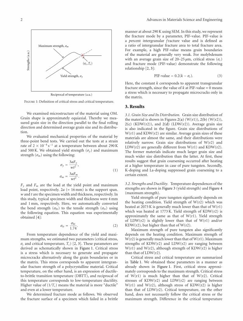
2 Advances in Materials Science and Engineering
Reciprocal of temperature (a.u.)
Stre
ngt
hs
(a.u
.)
(σc ,Tc)
Yield strength, σy
Maximum strength, σm
Figure 1: Definition of critical stress and critical temperature.
We examined microstructure of the material using OM.Grain shape is approximately equiaxial. Thereby we mea-sured grain size in the direction parallel to the final rollingdirection and determined average grain size and its distribu-tion.
We evaluated mechanical properties of the material bythree-point bend tests. We carried out the tests at a strainrate of 2 × 10⁻⁴ s−1 at a temperature between about 290 Kand 500 K. We obtained yield strength (σy) and maximumstrength (σm) using the following:
σy =3aFywt2
,
σm = 3aFmwt2
.
(1)
Fy and Fm are the load at the yield point and maximumload point, respectively. 2a (= 16 mm) is the support span.w and t are the specimen width and thickness, respectively. Inthis study, typical specimen width and thickness were 4 mmand 1 mm, respectively. Here, we automatically convertedthe bend strength (σbt) to the tensile strength (σtt) usingthe following equation. This equation was experimentallyobtained [4]:
σtt = σbt1.74
. (2)
From temperature dependence of the yield and maxi-mum strengths, we estimated two parameters (critical stress,σc and critical temperature, Tc) [2, 3]. These parameters arederived as schematically shown in Figure 1. Critical stressis a stress which is necessary to generate and propagatemicrocracks alternatively along the grain boundaries or inthe matrix. This stress corresponds to apparent intergran-ular fracture strength of a polycrystalline material. Criticaltemperature, on the other hand, is an expression of ductile-to-brittle transition temperature (DBTT), and reciprocal ofthis temperature corresponds to low-temperature ductility.Higher value of (1/Tc) means the material is more “ductile”and even at a lower temperature.
We determined fracture mode as follows. We observedthe fracture surface of a specimen which failed in a brittle
manner at about 290 K using SEM. In this study, we representthe fracture mode by a parameter, PIF-value. PIF-value isa percent intergranular f racture value and is defined asa ratio of intergranular fracture area to total fracture area.For example, a high PIF-value means grain boundariesof the material are generally very weak. For molybdenumwith an average grain size of 20–25 μm, critical stress (σc)and fracture mode (PIF-value) demonstrate the followingrelationship [2, 3]:
PIF-value = 0.2(k − σc). (3)
Here, the constant k corresponds to apparent transgranularfracture strength, since the value of k at PIF-value = 0 meansa stress which is necessary to propagate microcracks only inthe matrix.
3. Results
3.1. Grain Size and Its Distribution. Grain size distribution ofthe material is shown in Figures 2(a) (W(r1)), 2(b) (W(r2)),2(c) (KDW(r2)), and 2(d) (LDW(r2)). Average grain sizeis also indicated in the figure. Grain size distributions ofW(r1) and KDW(r2) are similar. Average grain sizes of thesematerials are almost the same, and their distributions wererelatively narrow. Grain size distributions of W(r2) andLDW(r2) are generally different from W(r1) and KDW(r2).The former materials indicate much larger grain size andmuch wider size distribution than the latter. At first, theseresults suggest that grain coarsening occurred after heatingat a higher temperature in case of pure tungsten. Secondly,K-doping and La-doping suppressed grain coarsening to acertain extent.
3.2. Strengths and Ductility. Temperature dependences of thestrengths are shown in Figure 3 (yield strength) and Figure 4(maximum strength).
Yield strength of pure tungsten significantly depends onthe heating condition. Yield strength of W(r2) which washeated at 2073 K is generally much lower than that of W(r1)which was heated at 1773 K. Yield strength of KDW(r2) isapproximately the same as that of W(r1). Yield strengthof LDW(r2) is slightly lower than that of W(r1) and/orKDW(r2), but higher than that of W(r2).
Maximum strength of pure tungsten also significantlydepends on the heating condition. Maximum strength ofW(r2) is generally much lower than that of W(r1). Maximumstrengths of KDW(r2) and LDW(r2) are ranging betweenW(r1) and W(r2), although strength of KDW(r2) is higherthan that of LDW(r2).
Critical stress and critical temperature are summarizedin Table 1. We obtained these parameters in a manner asalready shown in Figure 1. First, critical stress approxi-mately corresponds to the maximum strength. Critical stressof W(r1) is much higher than that of W(r2). Criticalstresses of KDW(r2) and LDW(r2) are ranging betweenW(r1) and W(r2), although stress of KDW(r2) is higherthan that of LDW(r2). Critical temperature, on the otherhand, does not necessarily follow the critical stress or themaximum strength. Difference in the critical temperature
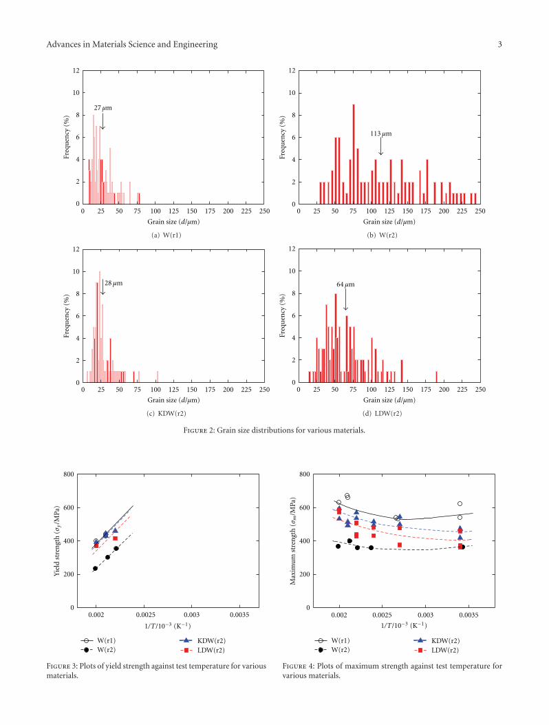
Advances in Materials Science and Engineering 3
0 25 50 75 100 125 150 175 200 225 2500
2
4
6
8
10
12Fr
equ
ency
(%)
27 μm
Grain size (d/μm)
(a) W(r1)
0 25 50 75 100 125 150 175 200 225 2500
2
4
6
8
10
12
Freq
uen
cy(%
)
113 μm
Grain size (d/μm)
(b) W(r2)
Grain size (d/μm)
0 25 50 75 100 125 150 175 200 225 250
28 μm
0
2
4
6
8
10
12
Freq
uen
cy(%
)
(c) KDW(r2)
0 25 50 75 100 125 150 175 200 225 2500
2
4
6
8
10
12
Freq
uen
cy(%
)64 μm
Grain size (d/μm)
(d) LDW(r2)
Figure 2: Grain size distributions for various materials.
0.002 0.003 0.00350.00250
200
400
600
800
Yie
ldst
ren
gth
(σy/M
Pa)
W(r1)W(r2)
KDW(r2)LDW(r2)
1/T/10−3 (K−1)
Figure 3: Plots of yield strength against test temperature for variousmaterials.
0.002 0.003 0.00350.0025
W(r1)W(r2)
KDW(r2)LDW(r2)
0
200
400
600
800
Max
imu
mst
ren
gth
(σm
/MPa
)
1/T/10−3 (K−1)
Figure 4: Plots of maximum strength against test temperature forvarious materials.
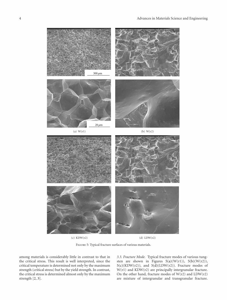
4 Advances in Materials Science and Engineering
300 μm
20 μm
(a) W(r1) (b) W(r2)
(c) KDW(r2) (d) LDW(r2)
Figure 5: Typical fracture surfaces of various materials.
among materials is considerably little in contrast to that inthe critical stress. This result is well interpreted, since thecritical temperature is determined not only by the maximumstrength (critical stress) but by the yield strength. In contrast,the critical stress is determined almost only by the maximumstrength [2, 3].
3.3. Fracture Mode. Typical fracture modes of various tung-sten are shown in Figures 5(a)(W(r1)), 5(b)(W(r2)),5(c)(KDW(r2)), and 5(d)(LDW(r2)). Fracture modes ofW(r1) and KDW(r2) are principally intergranular fracture.On the other hand, fracture modes of W(r2) and LDW(r2)are mixture of intergranular and transgranular fracture.
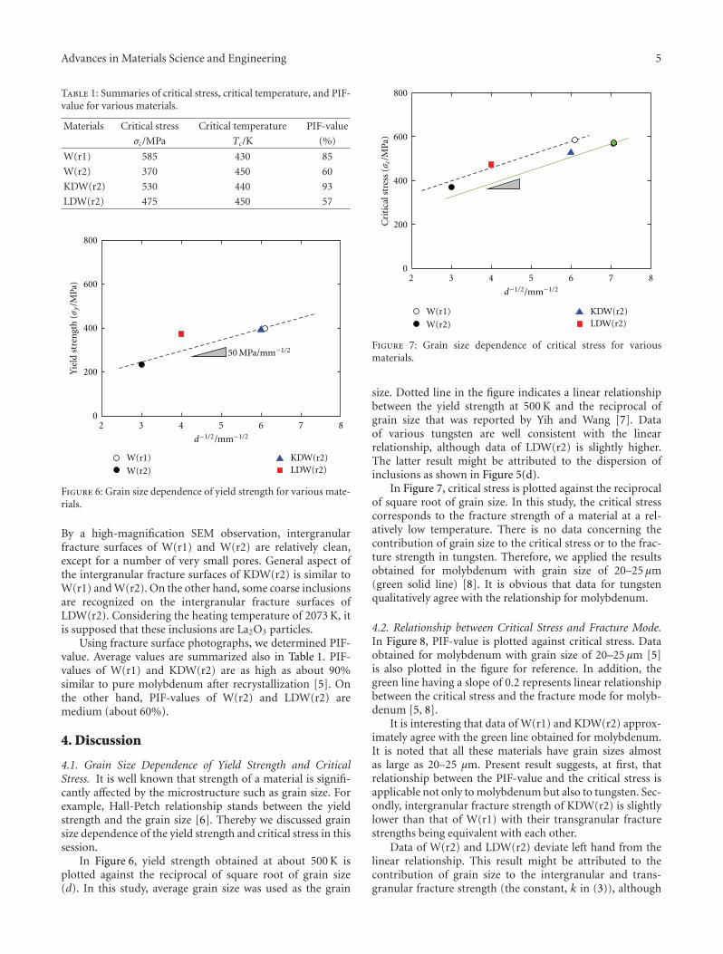
Advances in Materials Science and Engineering 5
Table 1: Summaries of critical stress, critical temperature, and PIF-value for various materials.
Materials Critical stress Critical temperature PIF-value
σc/MPa Tc/K (%)
W(r1) 585 430 85
W(r2) 370 450 60
KDW(r2) 530 440 93
LDW(r2) 475 450 57
2 3 4 5 6 7 80
200
400
600
800
W(r1)
W(r2)
KDW(r2)LDW(r2)
50 MPa/mm−1/2
Yie
ldst
ren
gth
(σy/M
Pa)
d−1/2/mm−1/2
Figure 6: Grain size dependence of yield strength for various mate-rials.
By a high-magnification SEM observation, intergranularfracture surfaces of W(r1) and W(r2) are relatively clean,except for a number of very small pores. General aspect ofthe intergranular fracture surfaces of KDW(r2) is similar toW(r1) and W(r2). On the other hand, some coarse inclusionsare recognized on the intergranular fracture surfaces ofLDW(r2). Considering the heating temperature of 2073 K, itis supposed that these inclusions are La2O3 particles.
Using fracture surface photographs, we determined PIF-value. Average values are summarized also in Table 1. PIF-values of W(r1) and KDW(r2) are as high as about 90%similar to pure molybdenum after recrystallization [5]. Onthe other hand, PIF-values of W(r2) and LDW(r2) aremedium (about 60%).
4. Discussion
4.1. Grain Size Dependence of Yield Strength and CriticalStress. It is well known that strength of a material is signifi-cantly affected by the microstructure such as grain size. Forexample, Hall-Petch relationship stands between the yieldstrength and the grain size [6]. Thereby we discussed grainsize dependence of the yield strength and critical stress in thissession.
In Figure 6, yield strength obtained at about 500 K isplotted against the reciprocal of square root of grain size(d). In this study, average grain size was used as the grain
2 3 4 5 6 7 8
W(r1)
W(r2)
KDW(r2)LDW(r2)
0
200
400
600
800
Cri
tica
lstr
ess
(σc/M
Pa)
d−1/2/mm−1/2
Figure 7: Grain size dependence of critical stress for variousmaterials.
size. Dotted line in the figure indicates a linear relationshipbetween the yield strength at 500 K and the reciprocal ofgrain size that was reported by Yih and Wang [7]. Dataof various tungsten are well consistent with the linearrelationship, although data of LDW(r2) is slightly higher.The latter result might be attributed to the dispersion ofinclusions as shown in Figure 5(d).
In Figure 7, critical stress is plotted against the reciprocalof square root of grain size. In this study, the critical stresscorresponds to the fracture strength of a material at a rel-atively low temperature. There is no data concerning thecontribution of grain size to the critical stress or to the frac-ture strength in tungsten. Therefore, we applied the resultsobtained for molybdenum with grain size of 20–25 μm(green solid line) [8]. It is obvious that data for tungstenqualitatively agree with the relationship for molybdenum.
4.2. Relationship between Critical Stress and Fracture Mode.In Figure 8, PIF-value is plotted against critical stress. Dataobtained for molybdenum with grain size of 20–25 μm [5]is also plotted in the figure for reference. In addition, thegreen line having a slope of 0.2 represents linear relationshipbetween the critical stress and the fracture mode for molyb-denum [5, 8].
It is interesting that data of W(r1) and KDW(r2) approx-imately agree with the green line obtained for molybdenum.It is noted that all these materials have grain sizes almostas large as 20–25 μm. Present result suggests, at first, thatrelationship between the PIF-value and the critical stress isapplicable not only to molybdenum but also to tungsten. Sec-ondly, intergranular fracture strength of KDW(r2) is slightlylower than that of W(r1) with their transgranular fracturestrengths being equivalent with each other.
Data of W(r2) and LDW(r2) deviate left hand from thelinear relationship. This result might be attributed to thecontribution of grain size to the intergranular and trans-granular fracture strength (the constant, k in (3)), although
6 Advances in Materials Science and Engineering
W(r1)
W(r2)
KDW(r2)LDW(r2)
200 400 600 800 10000
20
40
60
80
100
Mo(r1)
PIF
-val
ue
(%)
Critical stress (σc/MPa)
Figure 8: Plots of PIF-value against critical stress for various mate-rials.
200 400 600 800 1000
2
3
4
5
6
Critical stress (σc/MPa)
Du
ctili
ty,1
/Tc/1
0−3K−1
W(r1)
W(r2)
KDW(r2)LDW(r2)
Mo(r1)
Figure 9: Plots of ductility (1/Tc) against critical stress for variousmaterials.
contribution of grain size on the transgranular fracturestrength for tungsten has not been reported yet. Grain coars-ening concurrently induces lowering of transgranular frac-ture strength as well as lowering of intergranular fracturestrength. As a result, PIF-value is almost unchanged.
4.3. Plots of Critical Stress and Reciprocal of Critical Temper-ature. As already mentioned, the critical stress correspondsto the apparent intergranular fracture strength. On the otherhand, the critical temperature is an expression of ductile-to-brittle transition temperature (DBTT), and the reciprocal ofcritical temperature is a measure of ductility [2].
In Figure 9, reciprocal of critical temperature (ductil-ity) is plotted against critical stress. Data obtained formolybdenum [5] is also plotted in the figure for com-parison. At first, it is obvious that ductility of tungsten
is generally much lower than that of molybdenum. Thisresult is principally interpreted by the difference of yieldstrength between molybdenum and tungsten. It is knownthat yield strength of tungsten is much higher than thatof molybdenum at a given temperature with the grain sizebeing equivalent. The straight line in the figure indicatesthe temperature dependence of the yield strength. Secondly,intergranular fracture strength of tungsten is almost equiva-lent with that of molybdenum if the grain size is the same.
5. Summaries of Results
(1) Yield strength of tungsten principally depends on themicrostructure such as grain size. Yield strength oftungsten at a given temperature is much higher thanthat of molybdenum.
(2) Critical stress of tungsten depends not only on thegrain size but also on the intergranular fracturestrength. Critical stress of tungsten is almost equiv-alent with that of molybdenum if the grain size is thesame.
(3) Low-temperature ductility of tungsten is determinedboth by the yield strength and the maximum strength(critical stress). As a result, ductility of tungsten isgenerally much lower than that of molybdenum.
Acknowledgment
The authors greatly appreciate Dr. Tomohiro Takida andA.L.M.T. Corp for supplying pure tungsten and doped tung-sten materials.
References
[1] 8: Tungsten, in Behavior and Properties of Refractory Metals, T. E.Tietz and J. W. Wilson, Eds., pp. 274–330, University of TokyoPress, Tokyo, Japan, 1965.
[2] Y. Hiraoka, S. Yoshimura, and K. Takebe, “Effects of complexadditions of Re or Ti with C on the strength and ductility ofrecrystallized molybdenum,” International Journal of RefractoryMetals and Hard Materials, vol. 12, no. 5, pp. 261–268,1993.
[3] S. Yoshimura, Y. Hiraoka, and K. Takebe, “Effect of Ti in solu-tion on ductile-brittle transition characteristics of powder-met-allurgy molybdenum alloys,” Journal of the Japan Institute ofMetals, vol. 58, no. 7, pp. 734–739, 1994 (Japanese).
[4] T. Hoshika, S. Yoshimura, and Y. Hiraoka, “Evaluation of low-temperature fracture characteristics of molybdenum by meansof tensile tests and bend tests,” in Proceedings of the 14th inter-granular Plansee Sem, pp. 1018–1025, Tirol, Austria, 1997.
[5] T. Kadokura, Y. Hiraoka, Y. Yamamoto, and K. Okamot,“Change of mechanical property and fracture mode of molyb-denum by carbon addition,” Materials Transactions, vol. 51, no.7, pp. 1296–1301, 2010.
[6] N. J. Petch, “The cleavage strength of polycrystals,” The Journalof the Iron and Steel Institute, vol. 173, pp. 25–27, 1953.

Advances in Materials Science and Engineering 7
[7] S. W. H. Yih and C. T. Wang, Tungsten- Sources, Metallurgy,Properties, and Applications, Plenum, New York, NY, USA,1977.
[8] Y. Hiraoka, “Significant effect of carbon content in the low-temperature fracture behavior of molybdenum,” MaterialsTransactions, vol. 31, no. 10, pp. 861–864, 1990.
Hindawi Publishing CorporationAdvances in Materials Science and EngineeringVolume 2011, Article ID 136127, 10 pagesdoi:10.1155/2011/136127
Research Article
Young’s Modulus and Coefficient of Linear Thermal Expansion ofZnO Conductive and Transparent Ultra-Thin Films
Naoki Yamamoto, Hisao Makino, and Tetsuya Yamamoto
Research Institute, Kochi University of Technology, Tosayamada-cho, Kochi 782-8502, Japan
Correspondence should be addressed to Naoki Yamamoto, [email protected]
Received 29 March 2011; Accepted 17 May 2011
Academic Editor: Kin Ho Lo
Copyright © 2011 Naoki Yamamoto et al. This is an open access article distributed under the Creative Commons AttributionLicense, which permits unrestricted use, distribution, and reproduction in any medium, provided the original work is properlycited.
A new technique for measuring Young’s modulus of an ultra-thin film, with a thickness in the range of about 10 nm, was developedby combining an optical lever technique for measuring the residual stress and X-ray diffraction for measuring the strain in the film.The new technique was applied to analyze the mechanical properties of Ga-doped ZnO (GZO) films, that have become the focusof significant attention as a substitute material for indium-tin-oxide transparent electrodes. Young’s modulus of the as-depositedGZO films decreased with thickness; the values for 30 nm and 500 nm thick films were 205 GPa and 117 GPa, respectively. Thecoefficient of linear thermal expansion of the GZO films was measured using the new technique in combination with in-situresidual stress measurement during heat-cycle testing. GZO films with 30–100 nm thickness had a coefficient of linear thermalexpansion in the range of 4.3 × 10⁻⁶ – 5.6 × 10⁻⁶ ◦C−1.
1. Introduction
Optically transparent and conductive ZnO films, such as Ga-doped Zinc oxide (GZO) or Al-doped ZnO films, are attract-ing attention as alternative electrode materials to indium tinoxide (ITO), with good optical transparency and electricalconductive properties for liquid crystal displays (LCDs),flexible displays, touch-screens, and solar cells. Motivationsfor the development of ZnO transparent electrodes include(a) the scarcity of indium natural resources and (b) thetoxicity of indium. Indium is a rare element and ranks only61st in abundance in the Earth’s crust [1]. Also, in termsof toxicity, recently, indium was suspected to be a cause ofpulmonary diseases [2].
ZnO electrodes need to endure against mechanical forcescaused by the thermal processing steps during the manufac-ture of electronic devices such as flat panel displays, flexibledisplays, touch-screens, and LEDs, and by the expansion orshrinkage of parts caused by thermally severe circumstances(during summer and winter, e.g.) in the case of solar cells.These external forces could enhance the frequency of peelingor cracking in the elements composing the systems, such astransparent electrodes, during the fabrication or operation
of the devices. It is desired that the films used to form suchelectrodes have mechanically soft properties, because softmaterials can absorb external forces and avoid peeling andcracking of the films. To obtain such a film, various mechani-cal characteristics of the thin film, such as elasticity, plasticity,viscosity, brittleness, yield strength, and adhesiveness, shouldbe evaluated and be analyzed.
In these characteristics, Young’s modulus is one of themost important mechanical properties of a film. It is anintrinsic property of the film (material) that relates to theatomic bonding and the crystalline structure.
In this work, a new technique was developed for mea-suring the mechanical characteristics of an ultra-thin filmof a transparent electrode in LCD. Young’s moduli and thecoefficients of linear thermal expansion of GZO thin filmswere analyzed using the new technique.
2. Experimental
GZO films were prepared using two deposition methods: (1)conventional magnetron sputtering with dc power (dc MS)or with combined dc power/radiofrequency (rf) sputtering(rf + dc MS), and (2) reactive plasma deposition (RPD) [3].
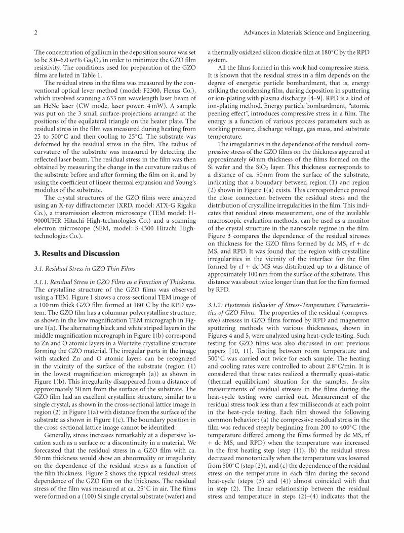
2 Advances in Materials Science and Engineering
The concentration of gallium in the deposition source was setto be 3.0–6.0 wt% Ga2O3 in order to minimize the GZO filmresistivity. The conditions used for preparation of the GZOfilms are listed in Table 1.
The residual stress in the films was measured by the con-ventional optical lever method (model: F2300, Flexus Co.),which involved scanning a 633 nm wavelength laser beam ofan HeNe laser (CW mode, laser power: 4 mW). A samplewas put on the 3 small surface-projections arranged at thepositions of the equilateral triangle on the heater plate. Theresidual stress in the film was measured during heating from25 to 500◦C and then cooling to 25◦C. The substrate wasdeformed by the residual stress in the film. The radius ofcurvature of the substrate was measured by detecting thereflected laser beam. The residual stress in the film was thenobtained by measuring the change in the curvature radius ofthe substrate before and after forming the film on it, and byusing the coefficient of linear thermal expansion and Young’smodulus of the substrate.
The crystal structures of the GZO films were analyzedusing an X-ray diffractometer (XRD, model: ATX-G RigakuCo.), a transmission electron microscope (TEM model: H-9000UHR Hitachi High-technologies Co.) and a scanningelectron microscope (SEM, model: S-4300 Hitachi High-technologies Co.).
3. Results and Discussion
3.1. Residual Stress in GZO Thin Films
3.1.1. Residual Stress in GZO Films as a Function of Thickness.The crystalline structure of the GZO films was observedusing a TEM. Figure 1 shows a cross-sectional TEM image ofa 100 nm thick GZO film formed at 180◦C by the RPD sys-tem. The GZO film has a columnar polycrystalline structure,as shown in the low magnification TEM micrograph in Fig-ure 1(a). The alternating black and white striped layers in themiddle magnification micrograph in Figure 1(b) correspondto Zn and O atomic layers in a Wurtzite crystalline structureforming the GZO material. The irregular parts in the imagewith stacked Zn and O atomic layers can be recognizedin the vicinity of the surface of the substrate (region (1)in the lowest magnification micrograph (a)) as shown inFigure 1(b). This irregularity disappeared from a distance ofapproximately 50 nm from the surface of the substrate. TheGZO film had an excellent crystalline structure, similar to asingle crystal, as shown in the cross-sectional lattice image inregion (2) in Figure 1(a) with distance from the surface of thesubstrate as shown in Figure 1(c). The boundary position inthe cross-sectional lattice image cannot be identified.
Generally, stress increases remarkably at a dispersive lo-cation such as a surface or a discontinuity in a material. Weforecasted that the residual stress in a GZO film with ca.50 nm thickness would show an abnormality or irregularityon the dependence of the residual stress as a function ofthe film thickness. Figure 2 shows the typical residual stressdependence of the GZO film on the thickness. The residualstress of the film was measured at ca. 25◦C in air. The filmswere formed on a (100) Si single crystal substrate (wafer) and
a thermally oxidized silicon dioxide film at 180◦C by the RPDsystem.
All the films formed in this work had compressive stress.It is known that the residual stress in a film depends on thedegree of energetic particle bombardment, that is, energystriking the condensing film, during deposition in sputteringor ion-plating with plasma discharge [4–9]. RPD is a kind ofion-plating method. Energy particle bombardment, “atomicpeening effect”, introduces compressive stress in a film. Theenergy is a function of various process parameters such asworking pressure, discharge voltage, gas mass, and substratetemperature.
The irregularities in the dependence of the residual com-pressive stress of the GZO films on the thickness appeared atapproximately 60 nm thickness of the films formed on theSi wafer and the SiO2 layer. This thickness corresponds toa distance of ca. 50 nm from the surface of the substrate,indicating that a boundary between region (1) and region(2) shown in Figure 1(a) exists. This correspondence provedthe close connection between the residual stress and thedistribution of crystalline irregularities in the film. This indi-cates that residual stress measurement, one of the availablemacroscopic evaluation methods, can be used as a monitorof the crystal structure in the nanoscale regime in the film.Figure 3 compares the dependence of the residual stresseson thickness for the GZO films formed by dc MS, rf + dcMS, and RPD. It was found that the region with crystallineirregularities in the vicinity of the interface for the filmformed by rf + dc MS was distributed up to a distance ofapproximately 100 nm from the surface of the substrate. Thisdistance was about twice longer than that for the film formedby RPD.
3.1.2. Hysteresis Behavior of Stress-Temperature Characteris-tics of GZO Films. The properties of the residual (compres-sive) stresses in GZO films formed by RPD and magnetronsputtering methods with various thicknesses, shown inFigures 4 and 5, were analyzed using heat-cycle testing. Suchtesting for GZO films was also discussed in our previouspapers [10, 11]. Testing between room temperature and500◦C was carried out twice for each sample. The heatingand cooling rates were controlled to about 2.8◦C/min. It isconsidered that these rates realized a thermally quasi-static(thermal equilibrium) situation for the samples. In-situmeasurements of residual stresses in the films during theheat-cycle testing were carried out. Measurement of theresidual stress took less than a few milliseconds at each pointin the heat-cycle testing. Each film showed the followingcommon behavior: (a) the compressive residual stress in thefilm was reduced steeply beginning from 200 to 400◦C (thetemperature differed among the films formed by dc MS, rf+ dc MS, and RPD) when the temperature was increasedin the first heating step (step (1)), (b) the residual stressdecreased monotonically when the temperature was loweredfrom 500◦C (step (2)), and (c) the dependence of the residualstress on the temperature in each film during the secondheat-cycle (steps (3) and (4)) almost coincided with thatin step (2). The linear relationship between the residualstress and temperature in steps (2)–(4) indicates that the
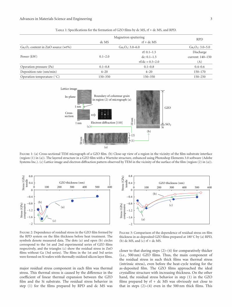
Advances in Materials Science and Engineering 3
Table 1: Specifications for the formation of GZO films by dc MS, rf + dc MS, and RPD.
Magnetron sputteringRPD
dc MS rf + dc MS
Ga2O3 content in ZnO source (wt%) Ga2O3: 3.0–6.0 Ga2O3: 3.0–5.0
Power (kW) 0.1–2.0rf: 0.1–1.5 Discharge
dc: 0.1–1.5 current: 140–150
rf/dc = 0.5–2.0 (A)
Operation pressure (Pa) 0.1–0.8 0.1–0.8 0.4–0.6
Deposition rate (nm/min) 4–20 4–20 150–170
Operation temperature (◦C) 150–350 150–350 150–250
(a)
(b)
SiO2
GZO
Si(c)
Boundary of columnar grainin region (2) of micrograph (a)
Cross-section
In-plane
Electron diffraction [110]
Lattice image
(2)
(1)
50n
m
10n
m
1 nm
1 nm
Figure 1: (a) Cross-sectional TEM micrograph of a GZO film. (b) Close-up view of a region in the vicinity of the film-substrate interface(region (1) in (a)). The layered structure in a GZO film with a Wurtzite structure, enhanced using Photoshop Elements 3.0 software (AdobeSystems Inc.). (c) Lattice image and electron diffraction pattern observed by TEM in the vicinity of the surface of the film (region (2) in (a)).
100 200 300 400 500 600
GZO thickness (nm)
Stre
ss(G
Pa)
Stre
ss(G
Pa)
00
−0.4
−0.8
−1.2
−1.6
−2
0.8
0.4
com
pres
sive
ten
sile
(a)
(b)
(c)
Figure 2: Dependence of residual stress in the GZO film formed bythe RPD system on the film thickness before heat treatment. Thesymbols denote measured data. The dots (a) and open (b) circlescorrespond to the 1st and 2nd experimental series of GZO filmsrespectively, and the triangles (c) show the residual stress in ZnOfilms without Ga (3rd series). The films in the 1st and 3rd serieswere formed on Si wafers with thermally oxidized silicon layer films.
major residual stress component in each film was thermalstress. This thermal stress is caused by the difference in thecoefficient of linear thermal expansion between the GZOfilm and the Si substrate. The residual stress behavior instep (1) for the films prepared by RPD and dc MS was
100 200 300 400 500 600
GZO thickness (nm)
Stre
ss(G
Pa)
Stre
ss(G
Pa)
00
−0.4
−0.8
−1.2
−1.6
−2
0.8
0.4
com
pres
sive
ten
sile
(a)
(b)
(c)
Figure 3: Comparison of the dependence of residual stress on filmthickness in as-deposited GZO films prepared at 180◦C by (a) RPD,(b) dc MS, and (c) rf + dc MS.
closer to that during steps (2)–(4) for comparatively thicker(i.e., 500 nm) GZO films. Thus, the main component ofthe residual stress in such thick films was thermal stress(intrinsic stress), even before the heat-cycle testing for theas-deposited film. The GZO films approached the idealcrystalline structure with increasing thickness. On the otherhand, the residual stress behavior in step (1) in the GZOfilms prepared by rf + dc MS was obviously not close tothat in steps (2)–(4) even in the 500 nm thick films. This
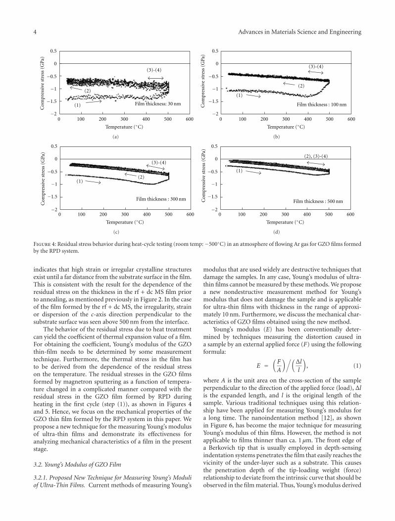
4 Advances in Materials Science and Engineering
0.5
0
−0.5
−1
−1.5
−2
Com
pres
sive
str
ess
(GPa
)
100 200 300 400 500 600
Temperature (◦C)
(1)
(2)
(3)-(4)
Film thickness: 30 nm
0
(a)
(1)
(2)
(3)-(4)
Film thickness : 100 nm
0.5
0
−0.5
−1
−1.5
−2100 200 300 400 500 600
Temperature (◦C)
0
Com
pres
sive
str
ess
(GPa
)
(b)
(1)
Film thickness : 300 nm
(2)
(3)-(4)
−2
0.5
0
−0.5
−1
−1.5
100 200 300 400 500 600
Temperature (◦C)
0
Com
pres
sive
str
ess
(GPa
)
(c)
(2), (3)-(4)
Film thickness : 500 nm
(1)
−2
0.5
0
−0.5
−1
−1.5
100 200 300 400 500 600
Temperature (◦C)
0
Com
pres
sive
str
ess
(GPa
)
(d)
Figure 4: Residual stress behavior during heat-cycle testing (room temp:−500◦C) in an atmosphere of flowing Ar gas for GZO films formedby the RPD system.
indicates that high strain or irregular crystalline structuresexist until a far distance from the substrate surface in the film.This is consistent with the result for the dependence of theresidual stress on the thickness in the rf + dc MS film priorto annealing, as mentioned previously in Figure 2. In the caseof the film formed by the rf + dc MS, the irregularity, strainor dispersion of the c-axis direction perpendicular to thesubstrate surface was seen above 500 nm from the interface.
The behavior of the residual stress due to heat treatmentcan yield the coefficient of thermal expansion value of a film.For obtaining the coefficient, Young’s modulus of the GZOthin-film needs to be determined by some measurementtechnique. Furthermore, the thermal stress in the film hasto be derived from the dependence of the residual stresson the temperature. The residual stresses in the GZO filmsformed by magnetron sputtering as a function of tempera-ture changed in a complicated manner compared with theresidual stress in the GZO film formed by RPD duringheating in the first cycle (step (1)), as shown in Figures 4and 5. Hence, we focus on the mechanical properties of theGZO thin film formed by the RPD system in this paper. Wepropose a new technique for the measuring Young’s modulusof ultra-thin films and demonstrate its effectiveness foranalyzing mechanical characteristics of a film in the presentstage.
3.2. Young’s Modulus of GZO Film
3.2.1. Proposed New Technique for Measuring Young’s Moduliof Ultra-Thin Films. Current methods of measuring Young’s
modulus that are used widely are destructive techniques thatdamage the samples. In any case, Young’s modulus of ultra-thin films cannot be measured by these methods. We proposea new nondestructive measurement method for Young’smodulus that does not damage the sample and is applicablefor ultra-thin films with thickness in the range of approxi-mately 10 nm. Furthermore, we discuss the mechanical char-acteristics of GZO films obtained using the new method.
Young’s modulus (E) has been conventionally deter-mined by techniques measuring the distortion caused ina sample by an external applied force (F) using the followingformula:
E =(F
A
)/(Δl
l
), (1)
where A is the unit area on the cross-section of the sampleperpendicular to the direction of the applied force (load), Δlis the expanded length, and l is the original length of thesample. Various traditional techniques using this relation-ship have been applied for measuring Young’s modulus fora long time. The nanoindentation method [12], as shownin Figure 6, has become the major technique for measuringYoung’s modulus of thin films. However, the method is notapplicable to films thinner than ca. 1 μm. The front edge ofa Berkovich tip that is usually employed in depth-sensingindentation systems penetrates the film that easily reaches thevicinity of the under-layer such as a substrate. This causesthe penetration depth of the tip-loading weight (force)relationship to deviate from the intrinsic curve that should beobserved in the film material. Thus, Young’s modulus derived
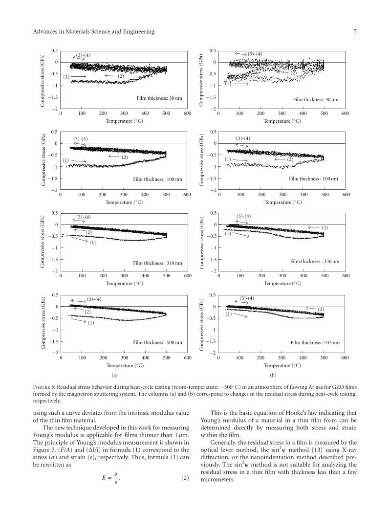
Advances in Materials Science and Engineering 5
0.5
0
−0.5
−1
−1.5
−2100 200 300 400 500 600
Temperature (◦C)
(1)
(1)
(1)
(1)
(2)
(2)
(2)
(2)
(3)-(4)
(3)-(4)
(3)-(4)
(3)-(4)
Film thickness : 100 nm
Film thickness: 30 nm
0
0.5
0
−0.5
−1
−1.5
−2
−2
−2
100 200 300 400 500 600
Temperature (◦C)
0
0.5
0
−0.5
−1
−1.5
100 200 300 400 500 600
Temperature (◦C)
0
0.5
0
−0.5
−1
−1.5
100 200 300 400 500 600
Temperature (◦C)
0
Film thickness : 500 nm
Film thickness : 310 nm
Com
pres
sive
str
ess
(GPa
)C
ompr
essi
ve s
tres
s (G
Pa)
Com
pres
sive
str
ess
(GPa
)C
ompr
essi
ve s
tres
s (G
Pa)
(a)
(1)
(1)
(1)
(1)
(2)
(2)
(2)
(2)
(3)-(4)
(3)-(4)
(3)-(4)
(3)-(4)
Film thickness : 100 nm
Film thickness: 30 nm
−2
−2
0.5
0
−0.5
−1
−1.5
100 200 300 400 500 600
Temperature (◦C)
0
0.5
0
−0.5
−1
−1.5
100 200 300 400 500 600
Temperature (◦C)
0
0.5
0
−0.5
−1
−1.5
−2100 200 300 400 500 600
Temperature (◦C)
0
0.5
0
−0.5
−1
−1.5
−2100 200 300 400 500 600
Temperature (◦C)
0
Film thickness : 533 nm
Film thickness : 330 nm
Com
pres
sive
str
ess
(GPa
)C
ompr
essi
ve s
tres
s (G
Pa)
Com
pres
sive
str
ess
(GPa
)C
ompr
essi
ve s
tres
s (G
Pa)
(b)
Figure 5: Residual stress behavior during heat-cycle testing (room-temperature: −500◦C) in an atmosphere of flowing Ar gas for GZO filmsformed by the magnetron sputtering system. The columns (a) and (b) correspond to changes in the residual stress during heat-cycle testing,respectively.
using such a curve deviates from the intrinsic modulus valueof the thin film material.
The new technique developed in this work for measuringYoung’s modulus is applicable for films thinner than 1 μm.The principle of Young’s modulus measurement is shown inFigure 7. (F/A) and (Δl/l) in formula (1) correspond to thestress (σ) and strain (ε), respectively. Thus, formula (1) canbe rewritten as
E = σ
ε. (2)
This is the basic equation of Hooke’s law indicating thatYoung’s modulus of a material in a thin film form can bedetermined directly by measuring both stress and strainwithin the film.
Generally, the residual stress in a film is measured by theoptical lever method, the sin2ψ method [13] using X-raydiffraction, or the nanoindentation method described pre-viously. The sin2ψ method is not suitable for analyzing theresidual stress in a thin film with thickness less than a fewmicrometers.
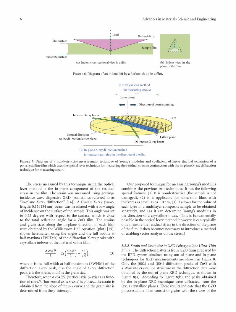
6 Advances in Materials Science and Engineering
Load Berkovich tip
Sample film
Film surface
Substrate surface
(a) Indent cross-sectional view in a film (b) Indent view in theplane of the film
Figure 6: Diagram of an indent left by a Berkovich tip in a film.
Normal directionto the di raction lattice plane
Incident X-ray beam
Di raction X-ray beam
Lattice plane
Laser beam
Direction of beam scanning
Film
(1) Optical lever method
for measuring stress σ
(2) In-plane X-ray di raction method
for measuring strain ε in the direction of the film
Figure 7: Diagram of a nondestructive measurement technique of Young’s modulus and coefficient of linear thermal expansion of apolycrystalline film which uses the optical lever technique for measuring the residual stress in conjunction with the in-plane X-ray diffractiontechnique for measuring strain.
The stress measured by this technique using the opticallever method is the in-plane component of the residualstress in the film. The strain was measured using grazing-incidence wave-dispersive XRD (sometimes referred to as“in-plane X-ray diffraction” [14]). A Cu-Kα X-ray (wave-length: 0.154184 nm) beam was irradiated with a low angleof incidence on the surface of the sample. This angle was setto 0.35 degrees with respect to the surface, which is closeto the total reflection angle for a ZnO film. The strainsand grain sizes along the in-plane direction in each filmwere obtained by the Williamson-Hall equation (plot) [15],shown hereinafter, using the angles and the full widths athalf maxima (FWHMs) of the diffraction X-ray peaks withcrystalline indexes of the material of the film:
σ cos θλ
= 2ε(
sin θ
λ
)+(
1δ
), (3)
where σ is the full width at half maximum (FWHM) of thediffraction X-ray peak, θ is the angle of X-ray diffractionpeak, ε is the strain, and δ is the grain size.
Therefore, when σ cos θ/λ (vertical axis: y-axis) as a func-tion of sin θ/λ (horizontal axis: x-axis) is plotted, the strain isobtained from the slope of the y-x curve and the grain size isdetermined from the y-intercept.
Our proposed technique for measuring Young’s moduluscombines the previous two techniques. It has the followingspecial features: (1) It is nondestructive (the sample is notdamaged), (2) it is applicable for ultra-thin films withthickness as small as ca. 10 nm, (3) it allows for the value ofeach layer in a multilayer composite sample to be obtainedseparately, and (4) it can determine Young’s modulus inthe direction of a crystalline index. (This is fundamentallypossible in the optical lever method; however, it can typicallyonly measure the residual stress in the direction of the planeof the film. It then becomes necessary to introduce a methodof enabling vector analysis on the stress.)
3.2.2. Strain and Grain size in GZO Polycrystalline Ultra-ThinFilms. The diffraction patterns from GZO films prepared bythe RPD system obtained using out-of-plane and in-planetechniques for XRD measurements are shown in Figure 8.Only the (002) and (004) diffraction peaks of ZnO witha Wurtzite crystalline structure in the diffraction data wereobtained by the out-of plane XRD technique, as shown inFigure 8(a). According to Figure 8(b), the peaks obtainedby the in-plane XRD technique were diffracted from the(xx0) crystalline planes. These results indicate that the GZOpolycrystalline films consist of grains with the c-axes of the
Advances in Materials Science and Engineering 7
Zn
O (
002)
Zn
O (
004)
35
30
25
20
15
10
5
020 30 40 50 60 70 80
Di raction angle 2θ (deg)
×103In
ten
sity
(cps
)
(a) Out-of-plane
Inte
nsi
ty(c
ps)
Zn
O (
100)
Zn
O (
110)
Zn
O (
200)
Zn
O (
210)
Zn
O (
300)
×103
9
8
7
6
5
4
3
2
1
020 40 60 80 100 120
Di raction angle 2θχ (deg)
(b) In-plane
Figure 8: Typical XRD profile of a GZO film with 150 nm thickness prepared at 180◦C using the RPD system. Profiles (a) and (b) wereobtained using out-of-plane and in-plane techniques for XRD measurements, respectively.
After heat-cycle testing
0 100 200 300 400 500 600
Before heat-cycle testing (as-deposited)
Gra
insi
ze(n
m)
0
10
20
30
40
Film thickness (nm)
(a) Grain size
Stra
in
0
0.001
0.002
0.003
0.004
0.005
0.006
0.007
0.008
After heat-cycle testing
Before heat-cycle testing (as-deposited)
0 100 200 300 400 500 600
Film thickness (nm)
(b) Strain
Figure 9: Average grain size and strain in the in-plane direction(a-axis of Wurtzite cell) as a function of film thickness.
Wurtzite crystalline cells oriented strictly along the normaldirection to the surface of the film.
The strains and grain sizes in polycrystalline GZO filmswere determined using (3) and the (x00) diffraction peaks inthe in-plane XRD patterns, respectively. The obtained strainis the component in the a-axis direction of the Wurtzitecrystalline cell of ZnO, that is, in the in-plain direction ofthe GZO film. Figure 9 shows the dependence of strain andgrain size in a GZO film on the film thickness before andafter the heat-cycle testing in the range of room temperatureto 500◦C. The grain size increased monotonically with the
film thickness. On the other hand, the strain decreasedwith increasing film thickness. These dependencies on thefilm thickness had good correspondence to cross-sectionalTEM micrographs shown previously in Figure 1. That is,region (1) close to the interface of the substrate had smallergrains and higher strains caused because the direction ofstacking of alternative Zn and O atomic layers (the directioncoincided with that of the c-axis of the Wurtzite crystallinecell) was not corresponding between each crystalline grain.To compare with it, the stacking directions were preciselyoriented among grains in region (2) at a far distance from thesurface of the substrate as shown in Figure 1. In particular,the dependence of strain on film thickness was consistentwith the dependence of the regular stacking of atomic layerson the distance from the interface. The strain characteristicsas a function of the GZO thickness in region (1) in Figure 1had a slope steeper than that in region (2).
We next discuss changes in the grain size and strainin a GZO film caused by the heat-cycle testing betweenroom temperature and 500◦C. The heat treatment had littleor no effect on grain growth in the in-plane direction(a-axis direction). On the other hand, the strain in theGZO film decreased remarkably by the heat-cycle testing.The reduction rate of strain in the film with ca. 100 nmthickness caused by the heat-cycle testing reached about50%. On the other hand, strain in a very thin film with ca.30 nm thickness was reduced only about 20% by the heattreatment. It is estimated that the heat-cycle testing conditionwas inadequate for releasing high strain caused by highlycrystalline irregularities in region (1). It is considered thata large number of crystalline defects were included in thevicinity of the interface with the substrate, such as in region(1) in Figure 1(a).
3.2.3. Young’s Modulus of GZO Thin Film. Young’s modulusof a GZO thin film was derived by substituting stress andstrain into (2) as mentioned in the previous section. Young’smodulus of the as-deposited GZO film depended on thefilm thickness as shown in Figure 10(a). Young’s modulus of
8 Advances in Materials Science and Engineering
an ultra-thin film, such as with 30 nm thickness, was about205 GPa. The film with 60 nm thickness had a maximummodulus of 300 GPa. This value decreased with increasingthickness of the film and reached a value of about 117 GPain the comparatively thick GZO film with 500 nm thickness.Generally, Young’s modulus shows a correlation with thehardness of a material. The hardness increases with thenumber of defects in a material. The defects pin atomic layerslip relative to other layers in a crystal due to an externalforce. Then, Young’s modulus in an ultra-thin film or inthe interfacial neighborhood with a large number of defectsbecomes larger than that of a thick film or at a far distancefrom the surface of a substrate. This dependence shown inFigure 10(a) is consistent with that of the distribution ofcrystalline irregularities or the dispersion of the stackingdirection of atomic layers within each grain shown in Figures1(a) and 1(b). The dependence of Young’s modulus of aGZO thin film on the film thickness after heat-cycle testingbetween room temperature and 500◦C is also shown inFigure 10(b). Young’s modulus of the comparatively thickerfilm with 500 nm thickness was reduced remarkably by aboutone digit and half from the value before heat-cycle testing.The reason why Young’s modulus of the thicker film withrelatively fewer defects decreased drastically is not yet clear.In an area away from the interface with the substrate, asshown in Figure 1(c), the Zn and O atomic layers at thepolycrystalline grain boundary were smoothly connected.The proportion of the volume of the region where a largenumber of defects existed in the vicinity of the surface ofthe substrate in the total volume of the film decreased withthe increasing thickness of the film. Then, the value obtainedfor Young’s modulus was affected by the ratio of region(2)/(region (1) + region (2)) as shown in Figure 1. In the caseof the 500 nm-thick GZO film, Young’s modulus measuredby this new technique was almost equal to that of region (2)with small amount of defects, since the volume of the regionbecame one order of magnitude larger than that of region(1) with a large number of defects. At this stage, we canonly speculate on the reason for why Young’s modulus of the500 nm thick was reduced significantly by heat-cycle testing.Very small numbers of defects existed at grain boundaries inregion (2), which was one of the main factors contributingto the modulus before heat treatment. The positions thatthe Zn and O atomic layers were connected continuouslysmoothly at the grain boundaries as shown in region (2) inFigures 1(a) and 1(c) and the positions that they were notconnected smoothly in region (1) existed in a film. Then,the crystalline defects occurred at the later positions in thegrain boundaries. This small number of defects in region(2) could disappear easily from the grain boundaries by heattreatment. As a result, Young’s modulus of thick films, suchas with 500 nm thickness, was reduced remarkably by heattreatment. The value was almost comparable with that of amaterial with low hardness, such as talc or calcium sulfate.
3.3. Coefficient of Linear Thermal Expansion of GZO Films.The thermal stress (σT) in a film is derived by the followingequation using the temperature (T) dependence of residualstress in the film:
0
50
100
150
200
250
300
350
0 100 200 300 400 500 600
Film thickness (nm)
You
ng’
sm
odu
lus
(GPa
)
(a)
102
103
101
100
After heat-cycle testing
Before heat-cycle testing (as-deposited)
0 100 200 300 400 500 600
Film thickness (nm)
You
ng’
sm
odu
lus
(GPa
)
(b)
Figure 10: Young’s modulus in the in-plane direction (a-axis ofWurtzite cell) of the GZO film formed by the RPD system asa function of film thickness. (a) Young’s modulus before heat-cycletesting (as-deposited). (b) Reduction in Young’s modulus value ofthe thin film caused by the heat-cycle testing. The same data in (a)is redrawn in (b).
σT = Δσ
ΔT. (4)
Using the thermal stress (σT) and Young’s modulus of thefilm, the coefficient of linear thermal expansion (α f ) of thefilm can be derived by the following:
α f =σT(
1− v f)
Ef+ αs. (5)
Here, v f , Ef , and αs represent the Poisson’s ratio of thefilm, Young’s Modulus of the film, and the coefficient oflinear thermal expansion of the substrate, respectively.
The thermal stress and the coefficient of linear thermalexpansion of the GZO films formed on the thermally oxi-dized Si wafer of a single crystal with a (100) crystallinesurface were obtained using the stress-temperature charac-teristics of the GZO film shown in Figure 4 and using (4)or (5). These material properties of the GZO films werederived from the stress-temperature characteristics in therange between room temperature and 250◦C taking intoaccount the following factors: (1) Young’s moduli of theGZO films derived using the measured residual stresses andstrains in the films mentioned in the previous section werevalues at room temperature, and (2) the highest processing
Advances in Materials Science and Engineering 9T
her
mal
stre
ss(M
Pa/d
eg)
0
0.2
0.4
0.6
0.8
1
Film thickness (nm)
0 100 200 300 400 500 600
(a)
Film thickness (nm)
0 100 200 300 400 500 60010−6
10−5
10−4
Coe
cien
tof
linea
rth
erm
alex
pan
sion
(b)
Figure 11: Thermal stress and coefficient of linear thermal expan-sion of GZO films formed by the RPD system as a function of filmthickness. (a) Dependence of thermal stress on film thickness, and(b) dependence of the coefficient of linear thermal expansion onfilm thickness.
temperature for manufacturing LCDs is generally limited toabout 250◦C since parts such as RGB (Red-Green-Blue) colorfilters that form LCDs are made of organic materials. Asshown in Figure 4, when the samples were heated up in thefirst cycle step (step (1)), the behavior of the residual stressas a function of the temperature was complicated. Then, thedependence of the residual stress on the temperature on thesecond heating stage (step (3)) was used for obtaining thethermal stress.
The value of 2.67 × 10⁻⁶ ◦C−1 at around 100◦C for thecoefficient of linear thermal expansion of Si as function oftemperature, reported by Okada and Tokumura [16], wasused for αs in (5). The thermal stress and the coefficient oflinear thermal expansion of a GZO film were then deter-mined as shown in Figure 11. The Poisson ratio of a GZOfilm was tentatively assigned as 0.3, which is the average ofthe Poisson ratios of ZnO picked as obtained from variousreports [17–23], because our technique had not yet reachedan applicable level to measure it in this stage. In the caseof a Poisson ratio of 0.1 lower or higher than 0.3 (Poissonratio: 0.2 or 0.4), the coefficient of linear thermal expansionincreases or decreases only about 7%.
The coefficients of linear thermal expansion of theGZO films with 30–100 nm thickness coincided with ourexpectation. On the other hand, the coefficient of linear
thermal expansion of the 500 nm thick film deviated far fromour expectation. It is not clear why an abnormal coefficient oflinear thermal expansion of the film with 500 nm thicknesswas obtained. We believe that this likely originated inthe excellent continuity of atomic layers at polycrystallineboundaries, similar to a singly crystal as shown in Fig-ure 1(c).
4. Summary
We developed a new technique for analyzing the mechanicalproperties of ultra-thin polycrystalline films. This methodfor measuring Young’s modulus of an ultra-thin film usedstress measurement by the optical lever technique togetherwith X-ray diffraction with an X-ray beam incident froman approximately total reflection angle (in-plane XRD tech-nique). This measurement technique is nondestructive anddoes not cause any damage to a film. Furthermore, the tech-nique can be applied for measuring Young’s modulus ofultra-thin films of various polycrystalline materials with 10–30 nm thickness.
In the dependence of the residual stress in the GZO thinfilms on film thickness, the maximum stress appeared inthe film with 50–60 nm thickness. This thickness coincidedexactly with the distance from the surface of the substrate,that changes from the region with irregular stacking direc-tions of alternate Zn and O atomic layers among columnargrains to the region consisting of grains with strictly alignedstacking direction. Thus, the residual stress represents infor-mation from nanoscale regions in crystalline films.
Young’s moduli of the GZO films showed a similar de-pendence on the film thickness. The maximum modulusreached a value of about 300 GPa. The modulus decreasedwith increasing thickness. The GZO film with 500 nm thick-ness had a Young’s modulus of 117 GPa. This value of themodulus is reasonable compared to values of 61–125 GPareported for ZnO films with 2-3 μm thickness measuredusing the nanoindentation technique [24]. The coefficientof linear thermal expansion of GZO films with 30–100 nmthickness was in the range of 4.3 × 10⁻⁶–5.6 × 10⁻⁶ ◦C−1.On the other hand, the film with 500 nm thickness had aremarkable high coefficient of 8.3× 10⁻⁵ ◦C−1. We estimatedthat this high value was related to the excellent continuityof Zn and O atomic layers in the in-plane direction (thedirection of the a-axis of the Wurtzite cell of ZnO) betweengrain boundaries similar to a single crystal. This excellentcontinuity also had a favorable effect on the low Young’smodulus and low residual stress.
The results indicate that the new measurement tech-nique for Young’s modulus of ultra-thin films is veryuseful. The mechanical properties of the GZO films formedby conventional magnetron sputtering are not discussed inthis paper. In a future paper, the characteristics of the filmswill be compared with those of the GZO films preparedby the RPD system. Furthermore, the technique will beapplied for developing ZnO transparent conductive filmsthat can resist external mechanical pressures during themanufacture of LCDs and testing long-term reliability of
10 Advances in Materials Science and Engineering
displays under external conditions of heating at 50–60◦C anda high humidity of 90–95%.
Acknowledgments
The authors would like to thank Professor Dr. Y. Yasudaof Center for Interdisciplinary Research, Tohoku University,Dr. T. Yamada of Guraduate school of Engineering, OsakaUniversity and Mr. M. Hakata of a former board memberof CASIO Computer Co., Ltd., for their encouragement,contributions and suggestions during the author’s researchon the mechanical properties of ultra-thin films. The authorsalso thank Dr. K. Takeda, Mr. T. Mine, and Mr. N. Sakumaof the Central Research Laboratory of Hitachi Co. Ltd. forproviding access to their analytical facilities, and Dr. K. Inabaof the X-ray Research Laboratory of Rigaku Corporation forvaluable advice throughout the course of this work. Thiswork was made possible by a grant for Collaboration ofRegional Entities for the Advancement of TechnologicalExcellence from the Japan Science and Technology Agency,and it was supported in part by a grant for the Developmentof Indium Substitute Materials for a Transparent ConductingElectrode in Rare Metal Substitute Materials DevelopmentProject from NEDO (New Energy and Industrial TechnologyDevelopment Organization).
References
[1] D. Kempthorne and M. D. Myers, Mineral Commodity Sum-maries 2007, United States Government Printing Office, Wash-ington, DC, USA, 2007.
[2] S. Homma, A. Miyamoto, S. Sakamoto, K. Kishi, N. Motoi,and K. Yoshimura, “Pulmonary fibrosis in an individual occu-pationally exposed to inhaled indium-tin oxide,” The EuropeanRespiratory Journal, vol. 25, no. 1, pp. 200–204, 2005.
[3] T. Yamamoto, T. Yamada, A. Miyake, H. Makino, and N.Yamamoto, “Ga-doped zinc oxide: an attractive potentialsubstitute for ITO, large-area coating, and control of electricaland optical properties on glass and polymer substrates,”Journal of the Society for Information Display, vol. 16, no. 7,pp. 713–719, 2008.
[4] R. S. Wagner, A. K. Sinha, T. T. Sheng, H. J. Levinstein, andF. B. Alexander, “Tungsten metallization for LSI applications,”Journal of Vacuum Science and Technology, vol. 11, pp. 582–590, 1974.
[5] J. A. Thornton and D. W. Hoffman, “Internal stresses in tita-nium, nickel, molybdenum, and tantalum films deposited bycylindrical magnetron sputtering,” Journal of Vacuum Scienceand Technology, vol. 14, pp. 164–168, 1977.
[6] D. W. Hoffman and J. A. Thornton, “The compressive stresstransition in Al, V, Zr, Nb and W metal films sputtered at lowworking pressures,” Thin Solid Films, vol. 45, no. 2, pp. 387–396, 1977.
[7] H. Windischmann, “Intrinsic stress in sputter-deposited thinfilms,” Critical Reviews in Solid State and Materials Sciences,vol. 17, no. 6, pp. 547–596, 1992.
[8] N. Yamamoto, H. Kume, S. Iwata et al., “Fabrication of highlyreliable tungsten gate MOS VLSI’s,” Journal of the Electrochem-ical Society, vol. 133, no. 2, pp. 401–407, 1986.
[9] R. E. Cuthrell, D. M. Mattox, C. R. Peeples, P. L. Dreike,and K. P. Lamppa, “Residual stress anisotropy, stress control,
and resistivity in post cathode magnetron sputter depositedmolybdenum films,” Journal of Vacuum Science and TechnologyA, vol. 6, no. 5, pp. 2914–2920, 1988.
[10] N. Yamamoto, T. Yamada, A. Miyake, H. Makino, S. Kishi-moto, and T. Yamamoto, “Relationship between residual stressand crystallographic structure in Ga-doped ZnO film,” Journalof the Electrochemical Society, vol. 155, no. 9, pp. J221–J225,2008.
[11] N. Yamamoto, H. Makino, T. Yamada et al., “Heat resistance ofGa-doped ZnO thin films for application as transparent elec-trodes in liquid crystal displays,” Journal of the ElectrochemicalSociety, vol. 157, no. 2, pp. J13–J20, 2010.
[12] E. B. Tadmor, R. Miller, and R. Phillips, “Nanoindentation andincipient plasticity,” Journal of Materials Research, vol. 14, no.6, pp. 2233–2250, 1999.
[13] P. S. Prevey, “X-ray diffraction residual stress techniques,” inMetals Handbook, vol. 10, pp. 380–392, American Society forMetals, Metals Park, Ohio, USA, 1986.
[14] B. K. Tanner, T. P. A. Hase, T. A. Lafford, and M. S. Goorsky,“Grazing incidence in-plane X-ray diffraction, internationalcentre for diffraction data,” Advances in X-Ray Analysis, vol.47, pp. 309–314, 2004.
[15] G. K. Williamson and W. H. Hall, “X-ray line broadening fromfiled aluminium and wolfram,” Acta Metallurgica, vol. 1, no. 1,pp. 23–31, 1953.
[16] Y. Okada and Y. Tokumura, “Precise determination of latticeparameter and thermal expansion coefficient of silicon 300 K–1500 K,” Journal of Applied Physics, vol. 56, no. 2, pp. 314–320,1984.
[17] S. Imai, M. Tokuyama, S. Hirose, G. J. Burger, T. S. J. Lam-merink, and J. H. J. Fluitman, “A thin-film piezoelectricimpact sensor array fabricated on a Si slider for measuringhead-disk interaction,” IEEE Transactions on Magnetics, vol.31, no. 6, pp. 3009–3011, 1995.
[18] H. K. Yoon and Y. S. Yu, “Hardness and elastic modulus ofZnO thin films fabricated by PLD method,” Key EngineeringMaterials, vol. 353–358, no. 4, pp. 2966–2969, 2007.
[19] I. Ozen, M. A. Gulgun, and M. Ozcan, “Self-induced crys-tallinity in RF magnetron sputtered ZnO thin films,” KeyEngineering Materials, vol. 264–268, pp. 1225–1228, 2004.
[20] H. C. Jung, H. K. Yoon, and Y. S. Yu, “Mechanical propertiesand process of ZnO deposited various substrates,” Key Engi-neering Materials, vol. 297–300, pp. 533–538, 2005.
[21] G. Cao and X. Chen, “Size dependence and orientation depen-dence of elastic properties of ZnO nanofilms,” InternationalJournal of Solids and Structures, vol. 45, no. 6, pp. 1730–1753,2008.
[22] G. Stan, C. V. Ciobanu, P. M. Parthangal, and R. F. Cook,“Diameter-dependent radial and tangential elastic moduli ofZnO nanowires,” Nano Letters, vol. 7, no. 12, pp. 3691–3697,2007.
[23] O. Kappertz, R. Drese, and M. Wuttig, “Correlation betweenstructure, stress and deposition parameters in direct currentsputtered zinc oxide films,” Journal of Vacuum Science andTechnology A, vol. 20, no. 6, pp. 2084–2095, 2002.
[24] T.-H. Fang, W.-J. Chang, and C.-M. Lin, “Nanoindentationcharacterization of ZnO thin films,” Materials Science and En-gineering A, vol. 452-453, pp. 715–720, 2007.
Hindawi Publishing CorporationAdvances in Materials Science and EngineeringVolume 2011, Article ID 940634, 9 pagesdoi:10.1155/2011/940634
Research Article
TEM Study of High-Temperature Precipitation ofDelta Phase in Inconel 718 Alloy
Moukrane Dehmas,1 Jacques Lacaze,2 Aliou Niang,2 and Bernard Viguier2
1 IJL-SI2M UMR 7198 CNRS-Nancy Universite-UPV Metz, Ecole des Mines de Nancy, Parc de Saurupt, CS 14234,54042 Nancy Cedex, France
2 Institut Carnot CIRIMAT, Universite de Toulouse, INP-ENSIACET, 4 allee Emile Monso, BP 44362, 31030 Toulouse Cedex 4, France
Correspondence should be addressed to Jacques Lacaze, [email protected]
Received 31 March 2011; Accepted 12 May 2011
Academic Editor: Joseph Lai
Copyright © 2011 Moukrane Dehmas et al. This is an open access article distributed under the Creative Commons AttributionLicense, which permits unrestricted use, distribution, and reproduction in any medium, provided the original work is properlycited.
Inconel 718 is widely used because of its ability to retain strength at up to 650◦C for long periods of time through coherentmetastable γ′′ Ni3Nb precipitation associated with a smaller volume fraction of γ′ Ni3Al precipitates. At very long ageing times atservice temperature, γ′′ decomposes to the stable Ni3Nb δ phase. This latter phase is also present above the γ′′ solvus and is usedfor grain control during forging of alloy 718. While most works available on δ precipitation have been performed at temperaturesbelow the γ′′ solvus, it appeared of interest to also investigate the case where δ phase precipitates directly from the fcc matrix free ofγ′′ precipitates. This was studied by X-ray diffraction and transmission electron microscopy (TEM). TEM observations confirmedthe presence of rotation-ordered domains in δ plates, and some unexpected contrast could be explained by double diffraction dueto overlapping phases.
1. Introduction
Alloy 718 is the most widely used material for turbinedisks and it is selected for many other applications as ahigh-strength material for temperatures up to 650◦C. Thisalloy was developed in the 60s when the former Fe-basedsuperalloys evolved towards Ni-based superalloys. Alloy 718contains both Fe and Ni alloyed with some Al and Ti, thoughthe most important addition is the refractory element Nb.A typical composition of alloy 718 is reported in Table 1. Itcontains a small amount of carbon as well as very low levelsof other species such as Si, Ta, Mn, Cu, S, B, P, and Mg, notlisted in Table 1 but generally controlled.
The strength of alloy 718 comes from coherent solid-stateprecipitates, which are for a small part γ′-Ni3Al but mostlyγ′′-Ni3Nb precipitates [1–6]. Both of these precipitates areordered forms of the fcc-A1 Ni-rich matrix: L12 in the case ofγ′ and DO22 in the case of γ′′. The solvus of these precipitatesis at about 900–920◦C as discussed previously [7]. Moreover,γ′′ precipitates are metastable while the stable form of Ni3Nbis the so-called delta phase which is orthorhombic. Forging
of 718 alloy is done at about 980◦C slightly below the solvusof the delta phase, in such a way that this phase is sufficientlyabundant to be effective in limiting grain growth but nottoo abundant to avoid significant Nb depletion in the matrixwhich would affect the subsequent strengthening by γ′′
precipitation. This latter precipitation is generally obtainedafter two successive periods of isothermal ageing at 750◦Cand 650◦C, respectively.
Precipitation of delta phase proceeds through a discon-tinuous reaction starting at grain boundaries and an intra-granular precipitation of thin plates. It has been reported thatthe former reaction predominates at low temperatures whilstthe latter is more characteristic of intermediate temperatures[2], but no systematic and quantitative study has beenperformed on that aspect. At high temperatures, both typesof precipitates may be observed as illustrated in Figure 1.
In fully strengthened material, precipitation of delta hasbeen studied for many years at both low and intermediatetemperatures as it corresponds to a dramatic decrease of themechanical properties of alloy 718. Kirman and Warrington[2] showed that the growth of δ at the expense of γ′′
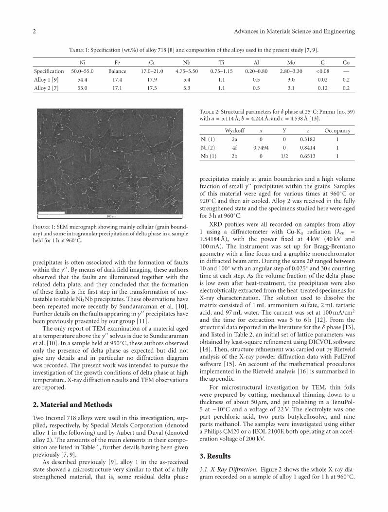
2 Advances in Materials Science and Engineering
Table 1: Specification (wt.%) of alloy 718 [8] and composition of the alloys used in the present study [7, 9].
Ni Fe Cr Nb Ti Al Mo C Co
Specification 50.0–55.0 Balance 17.0–21.0 4.75–5.50 0.75–1.15 0.20–0.80 2.80–3.30 <0.08 —
Alloy 1 [9] 54.4 17.4 17.9 5.4 1.1 0.5 3.0 0.02 0.2
Alloy 2 [7] 53.0 17.1 17.5 5.3 1.1 0.5 3.1 0.12 0.2
100 μm
Figure 1: SEM micrograph showing mainly cellular (grain bound-ary) and some intragranular precipitation of delta phase in a sampleheld for 1 h at 960◦C.
precipitates is often associated with the formation of faultswithin the γ′′. By means of dark field imaging, these authorsobserved that the faults are illuminated together with therelated delta plate, and they concluded that the formationof these faults is the first step in the transformation of me-tastable to stable Ni3Nb precipitates. These observations havebeen repeated more recently by Sundararaman et al. [10].Further details on the faults appearing in γ′′ precipitates havebeen previously presented by our group [11].
The only report of TEM examination of a material agedat a temperature above the γ′′ solvus is due to Sundararamanet al. [10]. In a sample held at 950◦C, these authors observedonly the presence of delta phase as expected but did notgive any details and in particular no diffraction diagramwas recorded. The present work was intended to pursue theinvestigation of the growth conditions of delta phase at hightemperature. X-ray diffraction results and TEM observationsare reported.
2. Material and Methods
Two Inconel 718 alloys were used in this investigation, sup-plied, respectively, by Special Metals Corporation (denotedalloy 1 in the following) and by Aubert and Duval (denotedalloy 2). The amounts of the main elements in their compo-sition are listed in Table 1, further details having been givenpreviously [7, 9].
As described previously [9], alloy 1 in the as-receivedstate showed a microstructure very similar to that of a fullystrengthened material, that is, some residual delta phase
Table 2: Structural parameters for δ phase at 25◦C: Pmmn (no. 59)with a = 5.114 A, b = 4.244 A, and c = 4.538 A [13].
Wyckoff x Y z Occupancy
Ni (1) 2a 0 0 0.3182 1
Ni (2) 4f 0.7494 0 0.8414 1
Nb (1) 2b 0 1/2 0.6513 1
precipitates mainly at grain boundaries and a high volumefraction of small γ′′ precipitates within the grains. Samplesof this material were aged for various times at 960◦C or920◦C and then air cooled. Alloy 2 was received in the fullystrengthened state and the specimens studied here were agedfor 3 h at 960◦C.
XRD profiles were all recorded on samples from alloy1 using a diffractometer with Cu-Kα radiation (λcu =1.54184 A), with the power fixed at 4 kW (40 kV and100 mA). The instrument was set up for Bragg-Brentanogeometry with a line focus and a graphite monochromatorin diffracted beam arm. During the scans 2θ ranged between10 and 100◦ with an angular step of 0.025◦ and 30 s countingtime at each step. As the volume fraction of the delta phaseis low even after heat-treatment, the precipitates were alsoelectrolytically extracted from the heat-treated specimens forX-ray characterization. The solution used to dissolve thematrix consisted of 1 mL ammonium sulfate, 2 mL tartaricacid, and 97 mL water. The current was set at 100 mA/cm2
and the time for extraction was 5 to 6 h [12]. From thestructural data reported in the literature for the δ phase [13],and listed in Table 2, an initial set of lattice parameters wasobtained by least-square refinement using DICVOL software[14]. Then, structure refinement was carried out by Rietveldanalysis of the X-ray powder diffraction data with FullProfsoftware [15]. An account of the mathematical proceduresimplemented in the Rietveld analysis [16] is summarized inthe appendix.
For microstructural investigation by TEM, thin foilswere prepared by cutting, mechanical thinning down to athickness of about 50 μm, and jet polishing in a TenuPol-5 at −10◦C and a voltage of 22 V. The electrolyte was onepart perchloric acid, two parts butylcellosolve, and nineparts methanol. The samples were investigated using eithera Philips CM20 or a JEOL 2100F, both operating at an accel-eration voltage of 200 kV.
3. Results
3.1. X-Ray Diffraction. Figure 2 shows the whole X-ray dia-gram recorded on a sample of alloy 1 aged for 1 h at 960◦C.
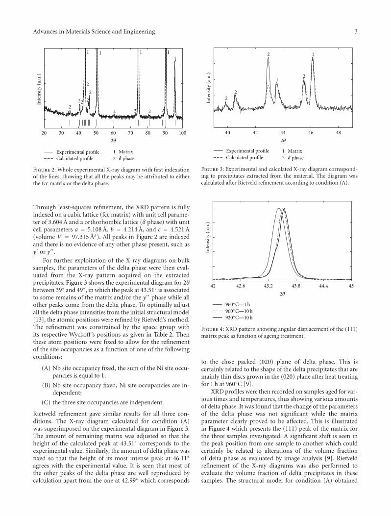
Advances in Materials Science and Engineering 3
20 30 40 50 60 70 80 90 100
2θ
Inte
nsi
ty(a
.u.)
Experimental profileCalculated profile
1 Matrix2 δ phase
2
1 1 1 11
22
2
2
2
2 2 2 2
Figure 2: Whole experimental X-ray diagram with first indexationof the lines, showing that all the peaks may be attributed to eitherthe fcc matrix or the delta phase.
Through least-squares refinement, the XRD pattern is fullyindexed on a cubic lattice (fcc matrix) with unit cell parame-ter of 3.604 A and a orthorhombic lattice (δ phase) with unitcell parameters a = 5.108 A, b = 4.214 A, and c = 4.521 A(volume V = 97.315 A3). All peaks in Figure 2 are indexedand there is no evidence of any other phase present, such asγ′ or γ′′.
For further exploitation of the X-ray diagrams on bulksamples, the parameters of the delta phase were then eval-uated from the X-ray pattern acquired on the extractedprecipitates. Figure 3 shows the experimental diagram for 2θbetween 39◦ and 49◦, in which the peak at 43.51◦ is associatedto some remains of the matrix and/or the γ′′ phase while allother peaks come from the delta phase. To optimally adjustall the delta phase intensities from the initial structural model[13], the atomic positions were refined by Rietveld’s method.The refinement was constrained by the space group withits respective Wyckoff ’s positions as given in Table 2. Thenthese atom positions were fixed to allow for the refinementof the site occupancies as a function of one of the followingconditions:
(A) Nb site occupancy fixed, the sum of the Ni site occu-pancies is equal to 1;
(B) Nb site occupancy fixed, Ni site occupancies are in-dependent;
(C) the three site occupancies are independent.
Rietweld refinement gave similar results for all three con-ditions. The X-ray diagram calculated for condition (A)was superimposed on the experimental diagram in Figure 3.The amount of remaining matrix was adjusted so that theheight of the calculated peak at 43.51◦ corresponds to theexperimental value. Similarly, the amount of delta phase wasfixed so that the height of its most intense peak at 46.11◦
agrees with the experimental value. It is seen that most ofthe other peaks of the delta phase are well reproduced bycalculation apart from the one at 42.99◦ which corresponds
40 42 44 46 48
Experimental profileCalculated profile
2θ
Inte
nsi
ty(a
.u.)
1 Matrix2
2
2
2
2
1
2
δ phase
Figure 3: Experimental and calculated X-ray diagram correspond-ing to precipitates extracted from the material. The diagram wascalculated after Rietveld refinement according to condition (A).
42 42.6 43.2 43.8 44.4 45
2θ
Inte
nsi
ty(a
.u.)
960◦C—1 h960◦C—10 h920◦C—10 h
Figure 4: XRD pattern showing angular displacement of the (111)matrix peak as function of ageing treatment.
to the close packed (020) plane of delta phase. This iscertainly related to the shape of the delta precipitates that aremainly thin discs grown in the (020) plane after heat treatingfor 1 h at 960◦C [9].
XRD profiles were then recorded on samples aged for var-ious times and temperatures, thus showing various amountsof delta phase. It was found that the change of the parametersof the delta phase was not significant while the matrixparameter clearly proved to be affected. This is illustratedin Figure 4 which presents the (111) peak of the matrix forthe three samples investigated. A significant shift is seen inthe peak position from one sample to another which couldcertainly be related to alterations of the volume fractionof delta phase as evaluated by image analysis [9]. Rietveldrefinement of the X-ray diagrams was also performed toevaluate the volume fraction of delta precipitates in thesesamples. The structural model for condition (A) obtained
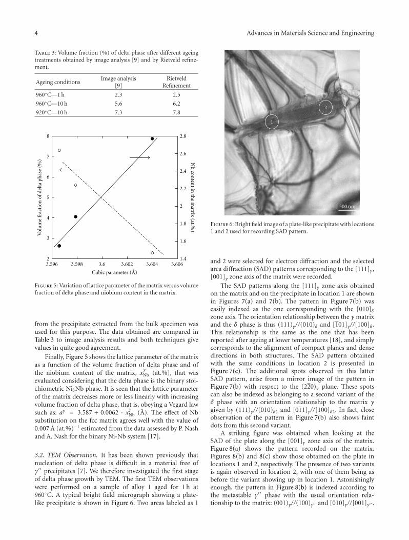
4 Advances in Materials Science and Engineering
Table 3: Volume fraction (%) of delta phase after different ageingtreatments obtained by image analysis [9] and by Rietveld refine-ment.
Ageing conditionsImage analysis
[9]Rietveld
Refinement
960◦C—1 h 2.3 2.5
960◦C—10 h 5.6 6.2
920◦C—10 h 7.3 7.8
2
3
4
5
6
7
8
1.4
1.6
1.8
2
2.2
2.4
2.6
2.8
3.596 3.598 3.6 3.602 3.604 3.606
Nb
conten
tin
the
matrix
(at.%)
Cubic parameter (A)
Vol
um
efr
acti
onof
delt
aph
ase
(%)
Figure 5: Variation of lattice parameter of the matrix versus volumefraction of delta phase and niobium content in the matrix.
from the precipitate extracted from the bulk specimen wasused for this purpose. The data obtained are compared inTable 3 to image analysis results and both techniques givevalues in quite good agreement.
Finally, Figure 5 shows the lattice parameter of the matrixas a function of the volume fraction of delta phase and ofthe niobium content of the matrix, x
γNb (at.%), that was
evaluated considering that the delta phase is the binary stoi-chiometric Ni3Nb phase. It is seen that the lattice parameterof the matrix decreases more or less linearly with increasingvolume fraction of delta phase, that is, obeying a Vegard lawsuch as: aγ = 3.587 + 0.0062 · xγNb (A). The effect of Nbsubstitution on the fcc matrix agrees well with the value of0.007 A (at.%)−1 estimated from the data assessed by P. Nashand A. Nash for the binary Ni-Nb system [17].
3.2. TEM Observation. It has been shown previously thatnucleation of delta phase is difficult in a material free ofγ′′ precipitates [7]. We therefore investigated the first stageof delta phase growth by TEM. The first TEM observationswere performed on a sample of alloy 1 aged for 1 h at960◦C. A typical bright field micrograph showing a plate-like precipitate is shown in Figure 6. Two areas labeled as 1
1
2
300 nm
Figure 6: Bright field image of a plate-like precipitate with locations1 and 2 used for recording SAD pattern.
and 2 were selected for electron diffraction and the selectedarea diffraction (SAD) patterns corresponding to the [111]γ,[001]γ zone axis of the matrix were recorded.
The SAD patterns along the [111]γ zone axis obtainedon the matrix and on the precipitate in location 1 are shownin Figures 7(a) and 7(b). The pattern in Figure 7(b) waseasily indexed as the one corresponding with the [010]δzone axis. The orientation relationship between the γ matrixand the δ phase is thus (111)γ//(010)δ and [101]γ//[100]δ .This relationship is the same as the one that has beenreported after ageing at lower temperatures [18], and simplycorresponds to the alignment of compact planes and densedirections in both structures. The SAD pattern obtainedwith the same conditions in location 2 is presented inFigure 7(c). The additional spots observed in this latterSAD pattern, arise from a mirror image of the pattern inFigure 7(b) with respect to the (220)γ plane. These spotscan also be indexed as belonging to a second variant of theδ phase with an orientation relationship to the matrix γgiven by (111)γ//(010)δ2 and [011]γ//[100]δ2. In fact, closeobservation of the pattern in Figure 7(b) also shows faintdots from this second variant.
A striking figure was obtained when looking at theSAD of the plate along the [001]γ zone axis of the matrix.Figure 8(a) shows the pattern recorded on the matrix,Figures 8(b) and 8(c) show those obtained on the plate inlocations 1 and 2, respectively. The presence of two variantsis again observed in location 2, with one of them being asbefore the variant showing up in location 1. Astonishinglyenough, the pattern in Figure 8(b) is indexed according tothe metastable γ′′ phase with the usual orientation rela-tionship to the matrix: (001)γ//(100)γ′′ and [010]γ//[001]γ′′ .
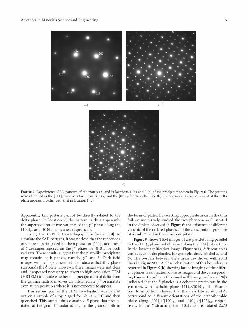
Advances in Materials Science and Engineering 5
000 220220
202
202
022
022
(a) (b)
(c)
Figure 7: Experimental SAD patterns of the matrix (a) and in locations 1 (b) and 2 (c) of the precipitate shown in Figure 6. The patternswere identified as the [111]γ zone axis for the matrix (a) and the [010]δ for the delta plate (b). In location 2, a second variant of the deltaphase appears together with that in location 1 (c).
Apparently, this pattern cannot be directly related to thedelta phase. In location 2, the pattern is thus apparentlythe superposition of two variants of the γ′′ phase along the[100]γ′′ and [010]γ′′ zone axes, respectively.
Using the CaRIne Crystallography software [19] tosimulate the SAD patterns, it was noticed that the reflectionsof γ′′ are superimposed on the δ phase for [111]γ and thoseof δ are superimposed on the γ′′ phase for [010]γ for bothvariants. These results suggest that the plate-like precipitatemay contain both phases, namely, γ′′ and δ. Dark fieldimages with γ′′ spots seemed to indicate that this phasesurrounds the δ plate. However, these images were not clearand it appeared necessary to resort to high-resolution TEM(HRTEM) to decide whether that precipitation of delta fromthe gamma matrix involves an intermediate γ′′ precipitateeven at temperatures where it is not expected to appear.
This second part of the TEM investigation was carriedout on a sample of alloy 2 aged for 3 h at 960◦C and thenquenched. This sample thus contained δ phase that precip-itated at the grain boundaries and in the grains, both in
the form of plates. By selecting appropriate areas in the thinfoil we successively studied the two phenomena illustratedin the δ plate observed in Figure 6: the existence of differentvariants of the ordered phases and the concomitant presenceof δ and γ′′ within the same precipitate.
Figure 9 shows TEM images of a δ platelet lying parallelto the (111)γ plane and observed along the [101]γ direction.In the low-magnification image, Figure 9(a), different areascan be seen in the platelet, for example, those labeled δ1 andδ2. The borders between these areas are shown with solidlines in Figure 9(a). A closer observation of this boundary isreported in Figure 9(b) showing lattice imaging of the differ-ent phases. Examination of these images and the correspond-ing Fourier transforms (obtained with ImageJ software [20])indicated that the δ platelet is a coherent precipitate in theγ matrix, with the habit plane (111)γ//(010)δ . The Fouriertransform patterns showed that the areas labeled δ1 and δ2
correspond to different orientations of the orthorhombicphase along [101]γ//[100]δ1 and [101]γ//[102]δ2, respec-tively. In the δ structure, the [102]δ axis is rotated 2π/3
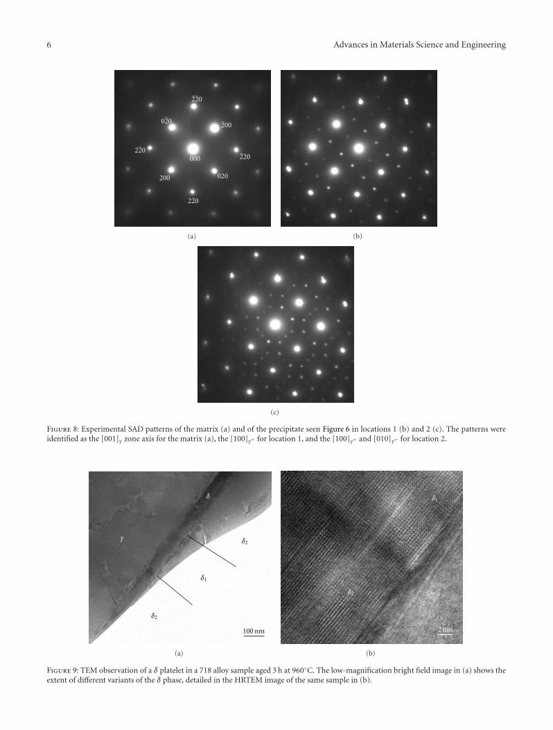
6 Advances in Materials Science and Engineering
000
220
220220
020
220
020
200
200
(a) (b)
(c)
Figure 8: Experimental SAD patterns of the matrix (a) and of the precipitate seen Figure 6 in locations 1 (b) and 2 (c). The patterns wereidentified as the [001]γ zone axis for the matrix (a), the [100]γ′′ for location 1, and the [100]γ′′ and [010]γ′′ for location 2.
100 nm
γ
δ
δ1
δ2
δ2
(a)
δ1
δ2
2 nm
(b)
Figure 9: TEM observation of a δ platelet in a 718 alloy sample aged 3 h at 960◦C. The low-magnification bright field image in (a) shows theextent of different variants of the δ phase, detailed in the HRTEM image of the same sample in (b).
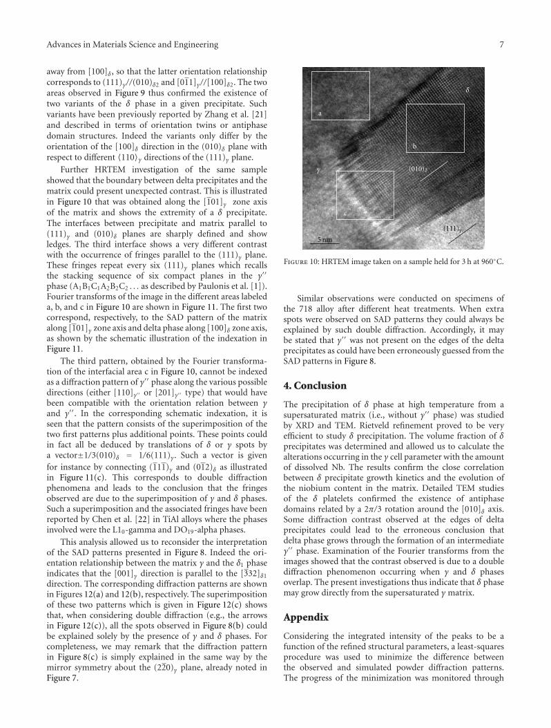
Advances in Materials Science and Engineering 7
away from [100]δ , so that the latter orientation relationshipcorresponds to (111)γ//(010)δ2 and [011]γ//[100]δ2. The twoareas observed in Figure 9 thus confirmed the existence oftwo variants of the δ phase in a given precipitate. Suchvariants have been previously reported by Zhang et al. [21]and described in terms of orientation twins or antiphasedomain structures. Indeed the variants only differ by theorientation of the [100]δ direction in the (010)δ plane withrespect to different 〈110〉γ directions of the (111)γ plane.
Further HRTEM investigation of the same sampleshowed that the boundary between delta precipitates and thematrix could present unexpected contrast. This is illustratedin Figure 10 that was obtained along the [101]γ zone axisof the matrix and shows the extremity of a δ precipitate.The interfaces between precipitate and matrix parallel to(111)γ and (010)δ planes are sharply defined and showledges. The third interface shows a very different contrastwith the occurrence of fringes parallel to the (111)γ plane.These fringes repeat every six (111)γ planes which recallsthe stacking sequence of six compact planes in the γ′′
phase (A1B1C1A2B2C2 . . . as described by Paulonis et al. [1]).Fourier transforms of the image in the different areas labeleda, b, and c in Figure 10 are shown in Figure 11. The first twocorrespond, respectively, to the SAD pattern of the matrixalong [101]γ zone axis and delta phase along [100]δ zone axis,as shown by the schematic illustration of the indexation inFigure 11.
The third pattern, obtained by the Fourier transforma-tion of the interfacial area c in Figure 10, cannot be indexedas a diffraction pattern of γ′′ phase along the various possibledirections (either [110]γ′′ or [201]γ′′ type) that would havebeen compatible with the orientation relation between γand γ′′. In the corresponding schematic indexation, it isseen that the pattern consists of the superimposition of thetwo first patterns plus additional points. These points couldin fact all be deduced by translations of δ or γ spots bya vector±1/3(010)δ = 1/6(111)γ. Such a vector is givenfor instance by connecting (111)γ and (012)δ as illustratedin Figure 11(c). This corresponds to double diffractionphenomena and leads to the conclusion that the fringesobserved are due to the superimposition of γ and δ phases.Such a superimposition and the associated fringes have beenreported by Chen et al. [22] in TiAl alloys where the phasesinvolved were the L10-gamma and DO19-alpha phases.
This analysis allowed us to reconsider the interpretationof the SAD patterns presented in Figure 8. Indeed the ori-entation relationship between the matrix γ and the δ1 phaseindicates that the [001]γ direction is parallel to the [332]δ1
direction. The corresponding diffraction patterns are shownin Figures 12(a) and 12(b), respectively. The superimpositionof these two patterns which is given in Figure 12(c) showsthat, when considering double diffraction (e.g., the arrowsin Figure 12(c)), all the spots observed in Figure 8(b) couldbe explained solely by the presence of γ and δ phases. Forcompleteness, we may remark that the diffraction patternin Figure 8(c) is simply explained in the same way by themirror symmetry about the (220)γ plane, already noted inFigure 7.
γ
δ
a
b
c
(111)γ
(010)δ
5 nm
Figure 10: HRTEM image taken on a sample held for 3 h at 960◦C.
Similar observations were conducted on specimens ofthe 718 alloy after different heat treatments. When extraspots were observed on SAD patterns they could always beexplained by such double diffraction. Accordingly, it maybe stated that γ′′ was not present on the edges of the deltaprecipitates as could have been erroneously guessed from theSAD patterns in Figure 8.
4. Conclusion
The precipitation of δ phase at high temperature from asupersaturated matrix (i.e., without γ′′ phase) was studiedby XRD and TEM. Rietveld refinement proved to be veryefficient to study δ precipitation. The volume fraction of δprecipitates was determined and allowed us to calculate thealterations occurring in the γ cell parameter with the amountof dissolved Nb. The results confirm the close correlationbetween δ precipitate growth kinetics and the evolution ofthe niobium content in the matrix. Detailed TEM studiesof the δ platelets confirmed the existence of antiphasedomains related by a 2π/3 rotation around the [010]δ axis.Some diffraction contrast observed at the edges of deltaprecipitates could lead to the erroneous conclusion thatdelta phase grows through the formation of an intermediateγ′′ phase. Examination of the Fourier transforms from theimages showed that the contrast observed is due to a doublediffraction phenomenon occurring when γ and δ phasesoverlap. The present investigations thus indicate that δ phasemay grow directly from the supersaturated γ matrix.
Appendix
Considering the integrated intensity of the peaks to be afunction of the refined structural parameters, a least-squaresprocedure was used to minimize the difference betweenthe observed and simulated powder diffraction patterns.The progress of the minimization was monitored through
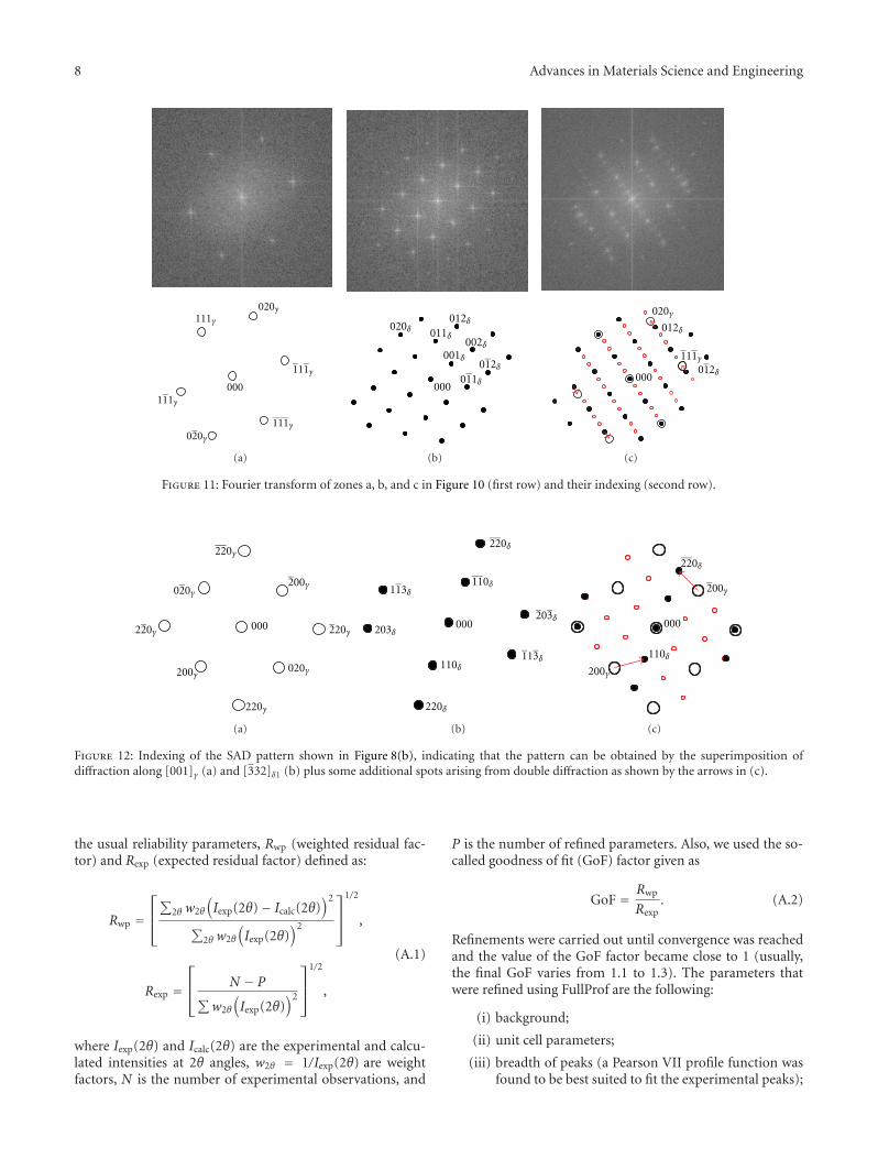
8 Advances in Materials Science and Engineering
000
111γ
111γ
111γ
020γ
020γ111γ
(a)
000
020δ
001δ002δ
011δ
011δ
012δ
012δ
(b)
000
020γ012δ
012δ
111γ
(c)
Figure 11: Fourier transform of zones a, b, and c in Figure 10 (first row) and their indexing (second row).
220γ
020γ
220γ
200γ
200γ
000 220γ
020γ
220γ
(a)
113δ
203δ
220δ
110δ
000
110δ
220δ
203δ
113δ
(b)
220δ
200γ
000
110δ200γ
(c)
Figure 12: Indexing of the SAD pattern shown in Figure 8(b), indicating that the pattern can be obtained by the superimposition ofdiffraction along [001]γ (a) and [332]δ1 (b) plus some additional spots arising from double diffraction as shown by the arrows in (c).
the usual reliability parameters, Rwp (weighted residual fac-tor) and Rexp (expected residual factor) defined as:
Rwp =⎡⎢⎣∑
2θ w2θ
(Iexp(2θ)− Icalc(2θ)
)2
∑2θ w2θ
(Iexp(2θ)
)2
⎤⎥⎦
1/2
,
Rexp =⎡⎢⎣ N − P∑
w2θ
(Iexp(2θ)
)2
⎤⎥⎦
1/2
,
(A.1)
where Iexp(2θ) and Icalc(2θ) are the experimental and calcu-lated intensities at 2θ angles, w2θ = 1/Iexp(2θ) are weightfactors, N is the number of experimental observations, and
P is the number of refined parameters. Also, we used the so-called goodness of fit (GoF) factor given as
GoF = Rwp
Rexp. (A.2)
Refinements were carried out until convergence was reachedand the value of the GoF factor became close to 1 (usually,the final GoF varies from 1.1 to 1.3). The parameters thatwere refined using FullProf are the following:
(i) background;
(ii) unit cell parameters;
(iii) breadth of peaks (a Pearson VII profile function wasfound to be best suited to fit the experimental peaks);
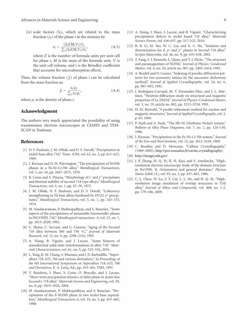
Advances in Materials Science and Engineering 9
(iv) scale factors (Si), which are related to the massfraction (xi) of the phase i in the mixture by
xi = (SiZMiVi)/ti∑i(SiZMiVi)/ti
, (A.3)
where Z is the number of formula units per unit cellfor phase i, M is the mass of the formula unit, V isthe unit cell volume, and t is the Brindley coefficientthat accounts for microabsorption effects.
Then, the volume fraction ( fi) of phase i can be calculatedfrom the mass fraction as:
fi = xi/ρi∑i xi/ρi
, (A.4)
where ρi is the density of phase i.
Acknowledgment
The authors very much appreciated the possibility of usingtransmission electron microscopes at CEMES and TEM-SCAN in Toulouse.
References
[1] D. F. Paulonis, J. M. Oblak, and D. S. Duvall, “Precipitation innickel-base alloy 718,” Trans. ASM, vol. 62, no. 3, pp. 611–622,1969.
[2] I. Kirman and D. H. Warrington, “The precipitation of Ni3Nbphases in a Ni-Fe-Cr-Nb alloy,” Metallurgical Transactions,vol. 1, no. 10, pp. 2667–2675, 1970.
[3] R. Cozar and A. Pineau, “Morphology of y’ and y” precipitatesand thermal stability of inconel 718 type alloys,” MetallurgicalTransactions, vol. 4, no. 1, pp. 47–59, 1973.
[4] J. M. Oblak, D. F. Paulonis, and D. S. Duvall, “Coherencystrengthening in Ni base alloys hardened by DO22 γ′ precip-itates,” Metallurgical Transactions, vol. 5, no. 1, pp. 143–153,1974.
[5] M. Sundararaman, P. Mukhopadhyay, and S. Banerjee, “Someaspects of the precipitation of metastable intermetallic phasesin INCONEL 718,” Metallurgical transactions. A, vol. 23, no. 7,pp. 2015–2028, 1992.
[6] C. Slama, C. Servant, and G. Cizeron, “Aging of the Inconel718 alloy between 500 and 750 ◦C,” Journal of MaterialsResearch, vol. 12, no. 9, pp. 2298–2316, 1997.
[7] A. Niang, B. Viguier, and J. Lacaze, “Some features ofanisothermal solid-state transformations in alloy 718,” Mate-rials Characterization, vol. 61, no. 5, pp. 525–534, 2010.
[8] L. Yang, K. M. Chang, S. Mannan, and J. D. Barbadillo, “Super-alloys 718, 625, 706 and various derivatives,” in Proceedings ofthe 6th International Symposium on Superalloys 718, 625, 706and Derivatives, E. A. Loria, Ed., pp. 353–365, TMS, 1997.
[9] V. Beaubois, J. Huez, S. Coste, O. Brucelle, and J. Lacaze,“Short term precipitation kinetics of delta phase in strain freeInconel∗ 718 alloy,” Materials Science and Engineering, vol. 20,no. 8, pp. 1019–1026, 2004.
[10] M. Sundararaman, P. Mukhopadhyay, and S. Banerjee, “Pre-cipitation of the δ-Ni3Nb phase in two nickel base superal-loys,” Metallurgical Transactions A, vol. 19, no. 3, pp. 453–465,1988.
[11] A. Niang, J. Huez, J. Lacaze, and B. Viguier, “Characterizingprecipitation defects in nickel based 718 alloy,” MaterialsScience Forum, vol. 636-637, pp. 517–522, 2010.
[12] R. B. Li, M. Yao, W. C. Liu, and X. C. He, “Isolation anddetermination for δ, γ′ and γ′′ phases in Inconel 718 alloy,”Scripta Materialia, vol. 46, no. 9, pp. 635–638, 2002.
[13] T. Fang, S. J. Kennedy, L. Quan, and T. J. Hicks, “The structureand paramagnetism of Ni3Nb,” Journal of Physics: CondensedMatter, vol. 4, no. 10, article no. 007, pp. 2405–2414, 1992.
[14] A. Boultif and D. Loueer, “Indexing of powder diffraction pat-terns for low-symmetry lattices by the successive dichotomymethod,” Journal of Applied Crystallography, vol. 24, no. 6,pp. 987–993, 1991.
[15] J. Rodriguez-Carvajal, M. T. Fernandez-Diaz, and J. L. Mar-tinez, “Neutron diffraction study on structural and magneticproperties of La 2NiO4,” Journal of Physics: Condensed Matter,vol. 3, no. 19, article no. 002, pp. 3215–3234, 1991.
[16] H. M. Rietveld, “A profile refinement method for nuclear andmagnetic structures,” Journal of Applied Crystallography, vol. 2,p. 65, 1969.
[17] P. Nash and A. Nash, “The Nb-Ni (Niobium-Nickel) system,”Bulletin of Alloy Phase Diagrams, vol. 7, no. 2, pp. 124–130,1986.
[18] I. Kirman, “Precipitation in the Fe-Ni-Cr-Nb system,” Journalof the Iron and Steel Institute, vol. 12, pp. 1612–1618, 1969.
[19] C. Boudias and D. Monceau, “CaRine Crystallography,”(1989–2003), http://pro.wanadoo.fr/carine.crystallography/.
[20] http://imagej.nih.gov/.
[21] J. P. Zhang, H. Q. Ye, K. H. Kuo, and S. Amelinckx, “High-resolution electron microscopy study of the domain structurein Ni//3Nb. II. Orientation and general domains,” PhysicaStatus Solidi (A), vol. 93, no. 2, pp. 457–462, 1986.
[22] C. L. Chen, W. Lu, Y. Y. Cui, L. L. He, and H. Q. Ye, “High-resolution image simulation of overlap structures in TiAlalloy,” Journal of Alloys and Compounds, vol. 468, no. 1-2,pp. 179–186, 2009.
Hindawi Publishing CorporationAdvances in Materials Science and EngineeringVolume 2011, Article ID 137387, 7 pagesdoi:10.1155/2011/137387
Research Article
γ′ Precipitation and Growth Kinetics inMechanically Alloyed Ni–Al
QingXin Tang, Shigeharu Ukai, Akinobu Minami, and Shigenari Hayashi
Materials Science and Engineering, Faculty of Engineering, Hokkaido University, N13, W-8, Kita-ku, Sapporo 060-8628, Japan
Correspondence should be addressed to Shigeharu Ukai, [email protected]
Received 27 March 2011; Accepted 13 May 2011
Academic Editor: Kin Ho Lo
Copyright © 2011 QingXin Tang et al. This is an open access article distributed under the Creative Commons Attribution License,which permits unrestricted use, distribution, and reproduction in any medium, provided the original work is properly cited.
The precipitation and growth kinetics of γ′ precipitates, which are strengthening factors in Ni-base oxide dispersion strengthened(ODS) superalloys, were investigated. The cuboidal-type γ′ precipitates are formed in conventional arc-melted Ni–Al alloys,whereas spherical-type precipitates are formed in the mechanically alloyed (MAed) specimens. The morphology is controlled by alattice misfit between the γ′ precipitates and the matrix at the aging temperature of 800◦C. The growth kinetics of the γ′ precipitatescan be followed by Ostwald ripening. The Arrhenius plot yielded a lower activation energy for the solute atom diffusion in MAedspecimens, which is attributed to their high dislocation density and nanosized grains.
1. Introduction
In jet engines and gas turbines, where Ni-base superalloyswith single crystals are currently used extensively as thematerials for blades, disks, and vanes, the inlet temperatureexceeds 1600◦C. Next-generation Ni-base superalloys areintensively being developed to improve thermal efficiency byincreasing inlet temperature; an oxide dispersion strength-ened (ODS) type of Ni-base superalloy could be candidateof such alloy. The strength of Ni-base ODS superalloys isaffected by both dispersed oxide particles and γ′ precipitateswith an L12 ordered structure. The coarsening behavior of γ′
precipitates in Ni-base superalloys on being subjected to hightemperature has been extensively investigated [1, 2]. Kusabi-raki et al. [3] reported that coarsening of γ′ precipitates inInconel X-750 follows Ostwald ripening, according to theLifshitz-Slyozov-Wagner (LSW) theory [4], which describesthat an increase in the radius of γ′ precipitates is proportionalto t1/3 (where t is the time). However, for mechanicallyalloyed (MAed) Ni-base ODS superalloys, experimentalinformation on γ′ precipitate behavior is extremely limited[5]. In this study, the precipitation and growth kinetics of γ′
precipitates were investigated for the Ni–15at%Al alloy, Ni–15at%Al–0.6at%Y2O3 alloy, and similar MA6000 fabricatedby ourselves by mechanical alloying and arc-melting as areference, focusing on the effects of MA and Y2O3 addition.
2. Experimental Procedures
The elemental powders in the size of about 100 μm wereprovided to make three kinds of target compositions: Ni–15at%Al, Ni–15at%Al–0.6at%Y2O3, and similar MA6000(Ni–15 wt%Cr–1.95 wt%Mo–4.45 wt%Al–2.9 wt%Ti–4 wt%W–1.9 wt%Ta–1 wt%Y2O3). These powders wereplaced in a pot 45 cc in volume together with stearic acidunder argon gas atmosphere in a glove box, and they weremechanically alloyed (MAed) by using a planetary-typeball mill (Fritsch P-6). The weight ratio of ball to powderwas set to 10 : 1. The mechanical alloying was processedfor 24 h. Subsequently, the MAed powders were sintered byhot-pressing (HP) at 1200◦C for 3 h. For comparison, theNi–15at%Al alloy was fabricated by arc-melting and wasthen heat-treated at 1200◦C for 72 h for forming a solidsolution. Here, as-MAed powders are referred to “MA,”the subsequently hot-pressed alloys of MAed powders arereferred to “MAHP,” and the arc-melted alloys are referredto “arc.”
In order to measure hardness changes due to γ′ pre-cipitation, MAed powders were enclosed in an ampouleunder vacuum, and the Vickers hardness test was conductedafter annealing at four different durations—3 min, 10 min,60 min, and 72 h at 800◦C. The particle size of the MAedpowders was about 50 μm. Hence, the Vickers hardness
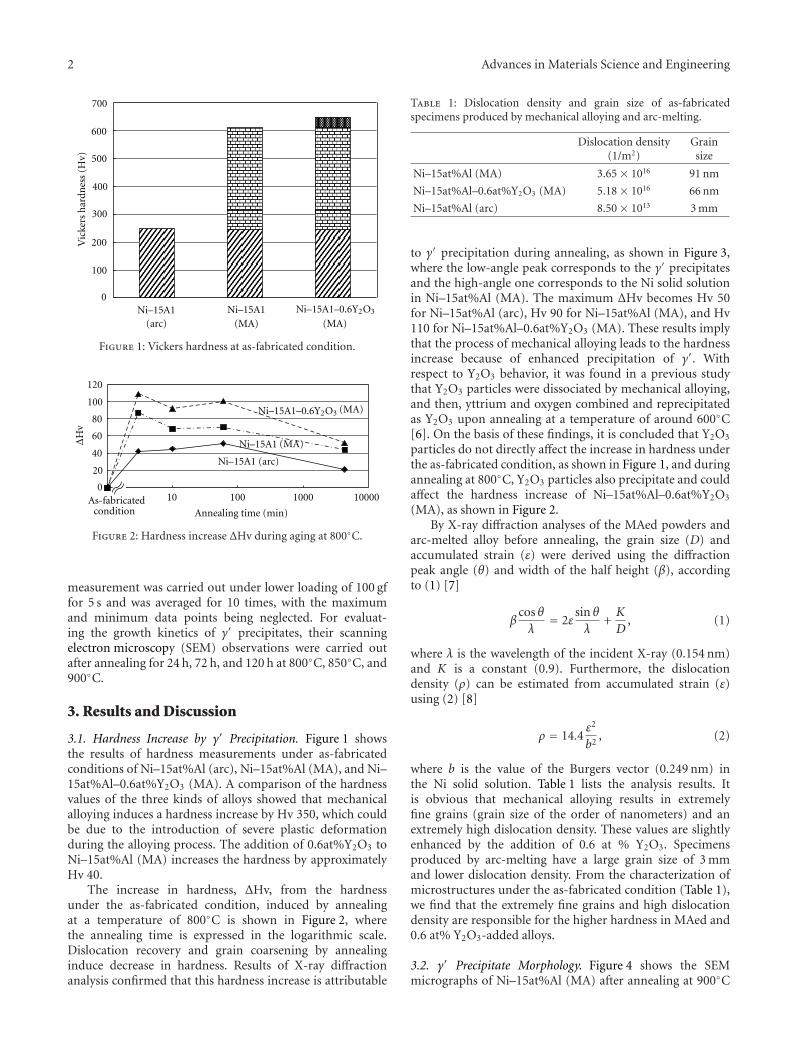
2 Advances in Materials Science and EngineeringV
icke
rsh
ardn
ess
(Hv)
0
100
200
300
400
500
600
700
(arc) (MA) (MA)Ni–15A1 Ni–15A1 Ni–15A1–0.6Y2O3
Figure 1: Vickers hardness at as-fabricated condition.
ΔH
v
0
20
40
60
80
100
120
10 100 1000 10000As-fabricatedcondition Annealing time (min)
(MA)
(MA)
Ni–15A1
Ni–15A1
(arc)
Ni–15A1–0.6Y2O3
Figure 2: Hardness increase ΔHv during aging at 800◦C.
measurement was carried out under lower loading of 100 gffor 5 s and was averaged for 10 times, with the maximumand minimum data points being neglected. For evaluat-ing the growth kinetics of γ′ precipitates, their scanningelectron microscopy (SEM) observations were carried outafter annealing for 24 h, 72 h, and 120 h at 800◦C, 850◦C, and900◦C.
3. Results and Discussion
3.1. Hardness Increase by γ′ Precipitation. Figure 1 showsthe results of hardness measurements under as-fabricatedconditions of Ni–15at%Al (arc), Ni–15at%Al (MA), and Ni–15at%Al–0.6at%Y2O3 (MA). A comparison of the hardnessvalues of the three kinds of alloys showed that mechanicalalloying induces a hardness increase by Hv 350, which couldbe due to the introduction of severe plastic deformationduring the alloying process. The addition of 0.6at%Y2O3 toNi–15at%Al (MA) increases the hardness by approximatelyHv 40.
The increase in hardness, ΔHv, from the hardnessunder the as-fabricated condition, induced by annealingat a temperature of 800◦C is shown in Figure 2, wherethe annealing time is expressed in the logarithmic scale.Dislocation recovery and grain coarsening by annealinginduce decrease in hardness. Results of X-ray diffractionanalysis confirmed that this hardness increase is attributable
Table 1: Dislocation density and grain size of as-fabricatedspecimens produced by mechanical alloying and arc-melting.
Dislocation density(1/m2)
Grainsize
Ni–15at%Al (MA) 3.65 × 10¹⁶ 91 nm
Ni–15at%Al–0.6at%Y2O3 (MA) 5.18 × 10¹⁶ 66 nm
Ni–15at%Al (arc) 8.50 × 10¹³ 3 mm
to γ′ precipitation during annealing, as shown in Figure 3,where the low-angle peak corresponds to the γ′ precipitatesand the high-angle one corresponds to the Ni solid solutionin Ni–15at%Al (MA). The maximum ΔHv becomes Hv 50for Ni–15at%Al (arc), Hv 90 for Ni–15at%Al (MA), and Hv110 for Ni–15at%Al–0.6at%Y2O3 (MA). These results implythat the process of mechanical alloying leads to the hardnessincrease because of enhanced precipitation of γ′. Withrespect to Y2O3 behavior, it was found in a previous studythat Y2O3 particles were dissociated by mechanical alloying,and then, yttrium and oxygen combined and reprecipitatedas Y2O3 upon annealing at a temperature of around 600◦C[6]. On the basis of these findings, it is concluded that Y2O3
particles do not directly affect the increase in hardness underthe as-fabricated condition, as shown in Figure 1, and duringannealing at 800◦C, Y2O3 particles also precipitate and couldaffect the hardness increase of Ni–15at%Al–0.6at%Y2O3
(MA), as shown in Figure 2.By X-ray diffraction analyses of the MAed powders and
arc-melted alloy before annealing, the grain size (D) andaccumulated strain (ε) were derived using the diffractionpeak angle (θ) and width of the half height (β), accordingto (1) [7]
βcos θλ
= 2εsin θ
λ+K
D, (1)
where λ is the wavelength of the incident X-ray (0.154 nm)and K is a constant (0.9). Furthermore, the dislocationdensity (ρ) can be estimated from accumulated strain (ε)using (2) [8]
ρ = 14.4ε2
b2, (2)
where b is the value of the Burgers vector (0.249 nm) inthe Ni solid solution. Table 1 lists the analysis results. Itis obvious that mechanical alloying results in extremelyfine grains (grain size of the order of nanometers) and anextremely high dislocation density. These values are slightlyenhanced by the addition of 0.6 at % Y2O3. Specimensproduced by arc-melting have a large grain size of 3 mmand lower dislocation density. From the characterization ofmicrostructures under the as-fabricated condition (Table 1),we find that the extremely fine grains and high dislocationdensity are responsible for the higher hardness in MAed and0.6 at% Y2O3-added alloys.
3.2. γ′ Precipitate Morphology. Figure 4 shows the SEMmicrographs of Ni–15at%Al (MA) after annealing at 900◦C
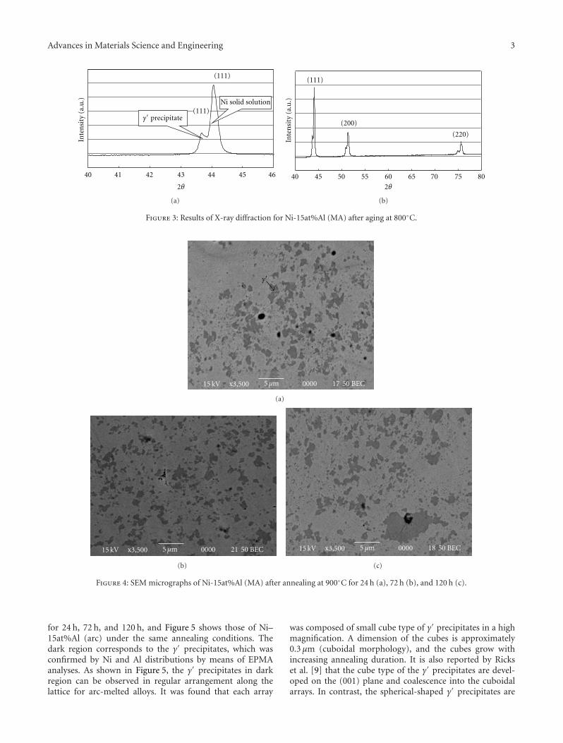
Advances in Materials Science and Engineering 3
40 41 42 43 44 45 46
Inte
nsi
ty(a
.u.)
γ precipitate
Ni solid solution
(111)
(111)
2θ
(a)
40 45 50 55 60 65 70 75 80
(220)
(200)
Inte
nsi
ty(a
.u.)
(111)
2θ
(b)
Figure 3: Results of X-ray diffraction for Ni-15at%Al (MA) after aging at 800◦C.
γ
15 kV x 5 μm 0000 17 50 BEC3,500
(a)
15 kV x 5 μm 0000 21 50 BEC3,500
(b)
15 kV x 5 μm 0000 18 50 BEC3,500
(c)
Figure 4: SEM micrographs of Ni-15at%Al (MA) after annealing at 900◦C for 24 h (a), 72 h (b), and 120 h (c).
for 24 h, 72 h, and 120 h, and Figure 5 shows those of Ni–15at%Al (arc) under the same annealing conditions. Thedark region corresponds to the γ′ precipitates, which wasconfirmed by Ni and Al distributions by means of EPMAanalyses. As shown in Figure 5, the γ′ precipitates in darkregion can be observed in regular arrangement along thelattice for arc-melted alloys. It was found that each array
was composed of small cube type of γ′ precipitates in a highmagnification. A dimension of the cubes is approximately0.3 μm (cuboidal morphology), and the cubes grow withincreasing annealing duration. It is also reported by Rickset al. [9] that the cube type of the γ′ precipitates are devel-oped on the (001) plane and coalescence into the cuboidalarrays. In contrast, the spherical-shaped γ′ precipitates are
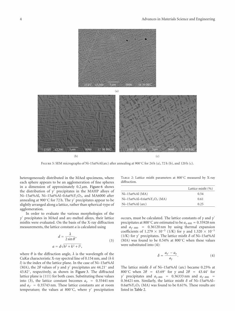
4 Advances in Materials Science and Engineering
15 kV x 5 μm 0000 16 50 BEC3,500
(a)
15 kV x 5 μm 0000 17 50 BEC3,500
(b)
15 kV x 5 μm 0000 17 50 BEC3,500
(c)
Figure 5: SEM micrographs of Ni-15at%Al(arc) after annealing at 900◦C for 24 h (a), 72 h (b), and 120 h (c).
heterogeneously distributed in the MAed specimens, whereeach sphere appears to be an agglomeration of fine spheresin a dimension of approximately 0.2 μm. Figure 6 showsthe distribution of γ′ precipitates in the MAHP alloys ofNi–15at%Al, Ni–15at%Al–0.6at%Y2O3, and MA6000 afterannealing at 900◦C for 72 h. The γ′ precipitates appear to beslightly arranged along a lattice, rather than spherical-type ofagglomeration.
In order to evaluate the various morphologies of theγ′ precipitates in MAed and arc-melted alloys, their latticemisfits were evaluated. On the basis of the X-ray diffractionmeasurements, the lattice constant a is calculated using
d = λ
2 sin θ,
a = d√h2 + k2 + l2,
(3)
where θ is the diffraction angle, λ is the wavelength of theCuKα characteristic X-ray spectral line of 0.154 nm, and (h kl) is the index of the lattice plane. In the case of Ni–15at%Al(MA), the 2θ values of γ and γ′ precipitates are 44.21◦ and43.82◦, respectively, as shown in Figure 3. The diffractedlattice plane is (111) for both cases. Substituting these valuesinto (3), the lattice constant becomes aγ = 0.35441 nmand aγ′ = 0.35743 nm. These lattice constants are at roomtemperature; the values at 800◦C, where γ′ precipitation
Table 2: Lattice misfit parameters at 800◦C measured by X-raydiffraction.
Lattice misfit (%)
Ni–15at%Al (MA) 0.54
Ni–15at%Al–0.6at%Y2O3 (MA) 0.61
Ni–15at%Al (arc) 0.25
occurs, must be calculated. The lattice constants of γ and γ′
precipitates at 800◦C are estimated to be aγ-800 = 0.35928 nmand aγ′-800 = 0.36120 nm by using thermal expansioncoefficients of 1.279 × 10⁻⁵ (1/K) for γ and 1.320 × 10⁻⁵
(1/K) for γ′ precipitates. The lattice misfit δ of Ni–15at%Al(MA) was found to be 0.54% at 800◦C when these valueswere substituted into (4):
δ = aγ′ − aγaγ
. (4)
The lattice misfit δ of Ni–15at%Al (arc) became 0.25% at800◦C when 2θ = 43.69◦ for γ and 2θ = 43.44◦ forγ′ precipitates and aγ-800 = 0.36333 nm and aγ′-800 =0.36421 nm. Similarly, the lattice misfit δ of Ni–15at%Al–0.6at%Y2O3 (MA) was found to be 0.61%. These results arelisted in Table 2.
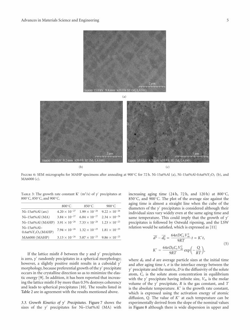
Advances in Materials Science and Engineering 5
S4800 15.0 kV 9.4 mm x20.0 k SE (M, LA100)
2 μm
(a)
S4800 15.0 kV 9.2 mm x20.0 k SE (M, LA100)
2 μm
(b)
S4800 15.0 kV 8.5 mm x10.0 k SE (M, LA100)
5 μm
(c)
Figure 6: SEM micrographs for MAHP specimens after annealing at 900◦C for 72 h. Ni-15at%Al (a), Ni-15at%Al-0.6at%Y2O3 (b), andMA6000 (c).
Table 3: The growth rate constant K′ (m3/s) of γ′ precipitates at800◦C, 850◦C, and 900◦C.
800◦C 850◦C 900◦C
Ni–15at%Al (arc) 4.20 × 10⁻²⁷ 1.99 × 10⁻²⁶ 9.22 × 10⁻²⁶
Ni–15at%Al (MA) 3.84 × 10⁻²⁷ 6.84 × 10⁻²⁷ 2.34 × 10⁻²⁶
Ni–15at%Al (MAHP) 3.91 × 10⁻²⁶ 7.33 × 10⁻²⁶ 1.23 × 10⁻²⁵
Ni–15at%Al–0.6at%Y2O3(MAHP)
7.94 × 10⁻²⁶ 1.32 × 10⁻²⁵ 1.81 × 10⁻²⁵
MA6000 (MAHP) 3.13 × 10⁻²⁶ 5.87 × 10⁻²⁵ 9.86 × 10⁻²⁵
If the lattice misfit δ between the γ and γ′ precipitatesis zero, γ′ randomly precipitates in a spherical morphology;however, a slightly positive misfit results in a cuboidal γ′
morphology, because preferential growth of the γ′ precipitateoccurs in the crystalline direction so as to minimize the elas-tic energy [9]. In addition, it has been reported that increas-ing the lattice misfit δ by more than 0.5% destroys coherencyand leads to spherical precipitates [10]. The results listed inTable 2 are in agreement with the results mentioned above.
3.3. Growth Kinetics of γ′ Precipitates. Figure 7 shows thesizes of the γ′ precipitates for Ni–15at%Al (MA) with
increasing aging time (24 h, 72 h, and 120 h) at 800◦C,850◦C, and 900◦C. The plot of the average size against theaging time is almost a straight line when the cube of thediameters of the γ′ precipitates is considered although theirindividual sizes vary widely even at the same aging time andsame temperature. This could imply that the growth of γ′
precipitates is followed by Ostwald ripening, and the LSWrelation would be satisfied, which is expressed as [11]
d3 − d30 =
64σDCeV 2m
9RTt = K ′t,
K ′ = 64σD0CeV 2m
9RTexp
(− QRT
),
(5)
where d0 and d are average particle sizes at the initial timeand after aging time t, σ is the interface energy between theγ′ precipitate and the matrix, D is the diffusivity of the soluteatom, Ce is the solute atom concentration in equilibriumwith the γ′ precipitate having infinite size, Vm is the molarvolume of the γ′ precipitate, R is the gas constant, and Tis the absolute temperature. K ′ is the growth rate constant,which is expressed using the activation energy of atomicdiffusion, Q. The value of K ′ at each temperature can beexperimentally derived from the slope of the nominal valuesin Figure 8 although there is wide dispersion in upper and
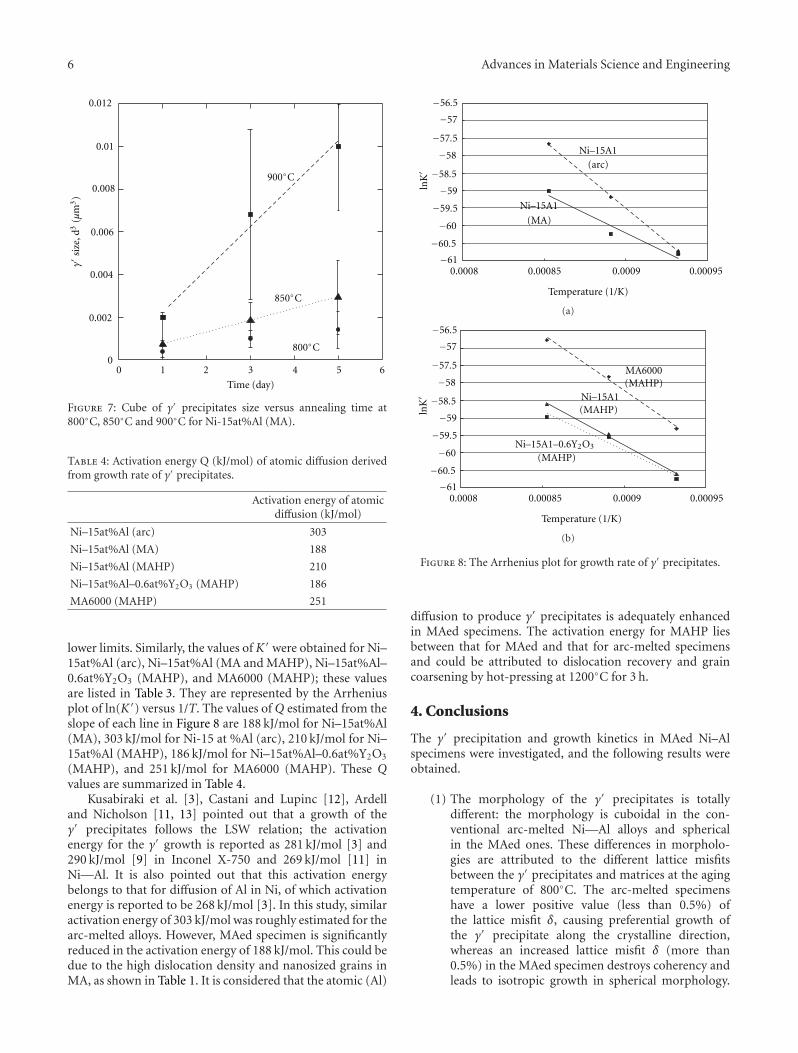
6 Advances in Materials Science and Engineering
0.002
0.004
0.006
0.008
0.01
0
0
.012
850◦C
800◦C
900◦C
γ s
ize,
d3(μ
m3)
0 1 2 3 4 5 6
Time (day)
Figure 7: Cube of γ′ precipitates size versus annealing time at800◦C, 850◦C and 900◦C for Ni-15at%Al (MA).
Table 4: Activation energy Q (kJ/mol) of atomic diffusion derivedfrom growth rate of γ′ precipitates.
Activation energy of atomicdiffusion (kJ/mol)
Ni–15at%Al (arc) 303
Ni–15at%Al (MA) 188
Ni–15at%Al (MAHP) 210
Ni–15at%Al–0.6at%Y2O3 (MAHP) 186
MA6000 (MAHP) 251
lower limits. Similarly, the values of K ′ were obtained for Ni–15at%Al (arc), Ni–15at%Al (MA and MAHP), Ni–15at%Al–0.6at%Y2O3 (MAHP), and MA6000 (MAHP); these valuesare listed in Table 3. They are represented by the Arrheniusplot of ln(K ′) versus 1/T. The values of Q estimated from theslope of each line in Figure 8 are 188 kJ/mol for Ni–15at%Al(MA), 303 kJ/mol for Ni-15 at %Al (arc), 210 kJ/mol for Ni–15at%Al (MAHP), 186 kJ/mol for Ni–15at%Al–0.6at%Y2O3
(MAHP), and 251 kJ/mol for MA6000 (MAHP). These Qvalues are summarized in Table 4.
Kusabiraki et al. [3], Castani and Lupinc [12], Ardelland Nicholson [11, 13] pointed out that a growth of theγ′ precipitates follows the LSW relation; the activationenergy for the γ′ growth is reported as 281 kJ/mol [3] and290 kJ/mol [9] in Inconel X-750 and 269 kJ/mol [11] inNi—Al. It is also pointed out that this activation energybelongs to that for diffusion of Al in Ni, of which activationenergy is reported to be 268 kJ/mol [3]. In this study, similaractivation energy of 303 kJ/mol was roughly estimated for thearc-melted alloys. However, MAed specimen is significantlyreduced in the activation energy of 188 kJ/mol. This could bedue to the high dislocation density and nanosized grains inMA, as shown in Table 1. It is considered that the atomic (Al)
−61
−60.5
−60
−59.5
−59
−58.5
−58
−57.5
−57
−56.5
lnK
0.0008 0.00085 0.0009 0.00095
Temperature (1/K)
(arc)
(MA)
Ni–15A1
Ni–15A1
(a)
−61
−60.5
−60
−59.5
−59
−58.5
−58
−57.5
−57
−56.5
lnK
0.0008
(MAHP)
(MAHP)
(MAHP)
Temperature (1/K)
MA6000
0.00085 0.0009 0.00095
Ni–15A1
Ni–15A1–0.6Y2O3
(b)
Figure 8: The Arrhenius plot for growth rate of γ′ precipitates.
diffusion to produce γ′ precipitates is adequately enhancedin MAed specimens. The activation energy for MAHP liesbetween that for MAed and that for arc-melted specimensand could be attributed to dislocation recovery and graincoarsening by hot-pressing at 1200◦C for 3 h.
4. Conclusions
The γ′ precipitation and growth kinetics in MAed Ni–Alspecimens were investigated, and the following results wereobtained.
(1) The morphology of the γ′ precipitates is totallydifferent: the morphology is cuboidal in the con-ventional arc-melted Ni—Al alloys and sphericalin the MAed ones. These differences in morpholo-gies are attributed to the different lattice misfitsbetween the γ′ precipitates and matrices at the agingtemperature of 800◦C. The arc-melted specimenshave a lower positive value (less than 0.5%) ofthe lattice misfit δ, causing preferential growth ofthe γ′ precipitate along the crystalline direction,whereas an increased lattice misfit δ (more than0.5%) in the MAed specimen destroys coherency andleads to isotropic growth in spherical morphology.
Advances in Materials Science and Engineering 7
The hardness increase induced by the γ′ precipitatesduring aging is accelerated in the MAed specimens.
(2) The growth kinetics of the γ′ precipitates can beexpressed by Ostwald ripening. On the basis of theLSW theory, the activation energy for the γ′ precip-itate growth was derived from the Arrhenius plot:303 kJ/mol for the arc-melted specimens, 188 kJ/molfor the MAed specimens, 210 kJ/mol for Ni–15at%Al(MAHP), 186 kJ/mol for Ni–15at%Al–0.6at%Y2O3
(MAHP), and 251 kJ/mol for the MAHP specimens.The lower activation energy for solute diffusion inthe MAed specimen could be attributed to the highdislocation density and nanosized grains.
Acknowledgment
The authors are grateful to Tanikawa Fund Promotion ofThermal Technology for supporting this work.
References
[1] A. Maheshwari and A. J. Ardell, “Anomalous coarseningbehavior of small volume fractions of Ni3Al precipitates inbinary Ni–Al alloys,” Acta Metallurgica Et Materialia, vol. 40,no. 10, pp. 2661–2667, 1992.
[2] A. K. Sinha and J. J. Moore, “Study of precipitation andgrowth of γ′ and dislocation structure in Inconel X-750,”Metallography, vol. 19, no. 1, pp. 75–86, 1986.
[3] K. Kusabiraki, H. Nagahama, L. Wang, and T. Ooka, “Growthof γ′ precipitates in nickel-base superalloy,” Tetsu-To-Hagane,vol. 75, no. 8, pp. 1354–1361, 1989 (Japanese).
[4] I. M. Lifshitz and V. V. Slyozov, “The kinetics of precipitationfrom supersaturated solid solutions,” Journal of Physics andChemistry of Solids, vol. 19, no. 1-2, pp. 35–50, 1961.
[5] HO. J. Ryu, S. H. Hong, J. Weber, and J. H. Tundermann,“Effect of elastic interaction energy on coarsening of γ′ pre-cipitates in a mechanically alloyed ODS Ni-base superalloy,”Journal of Materials Science, vol. 34, no. 2, pp. 329–336, 1999.
[6] T. Hoshino, S. Ukai, and S. Hayashi, in Proceedings of the 5thASM Heat Treatment and Surface Engineering Conference inEurope, pp. 643–646, 2000.
[7] W. H. Hall, The Journal of the Institute of Metals, vol. 75, p.1127, 1950.
[8] G. K. Williamson and R. E. Smallman, “III. Dislocationdensities in some annealed and cold-worked metals frommeasurements on the X-ray debye-scherrer spectrum,” Philo-sophical Magazine, vol. 1, pp. 34–46, 1956.
[9] R. A. Ricks, A. J. Porter, and R. C. Ecob, “The growth of γ′precipitates in nickel-base superalloys,” Acta Metallurgica, vol.31, no. 1, pp. 43–53, 1983.
[10] R. C. Reed, The Super Alloys, Fundamentals and Applications,Cambridge University Press, Cambridge, UK, 2005.
[11] A. J. Ardell and R. B. Nicholson, “On the modulated structureof aged Ni-Al alloys. with an Appendix On the elasticinteraction between inclusions by J. D. Eshelby Cavendish Lab-oratory, University of Cambridge, England,” Acta Metallurgica,vol. 14, no. 10, pp. 1295–1309, 1966.
[12] C. Castani and V. Lupinc, “Solution heat treatment, aging andmicrostructure of inconel X-750,” Metallurgia Italiana, vol. 69,no. 7-8, pp. 306–311, 1977.
[13] A. J. Ardell and R. B. Nicholson, “The coarsening of γ’ in Ni-Alalloys,” Journal of Physics and Chemistry of Solids, vol. 27, no.11-12, pp. 1793–1794, 1966.