TW9910 – Low Power NTSC/PAL/SECAM Video Decoder … · TW9910 TECHWELL, INC. 6 REV. A 09/21/2006...
71
TECHWELL, INC. 1 REV. A 09/21/2006 Techwell, Inc. TW9910 – Low Power NTSC/PAL/SECAM Video Decoder with VBI Slicer Data Sheet Techwell Confidential. Information may change without notice. Disclaimer This document provides technical information for the user. Techwell, Inc. reserves the right to modify the information in this document as necessary. The customer should make sure that they have the most recent data sheet version. Techwell, Inc. holds no responsibility for any errors that may appear in this document. Customers should take appropriate action to ensure their use of the products does not infringe upon any patents. Techwell, Inc. respects valid patent rights of third parties and does not infringe upon or assist others to infringe upon such rights.
Transcript of TW9910 – Low Power NTSC/PAL/SECAM Video Decoder … · TW9910 TECHWELL, INC. 6 REV. A 09/21/2006...

TECHWELL, INC. 1 REV. A 09/21/2006
Techwell, Inc.
TW9910 – Low Power NTSC/PAL/SECAM Video Decoder with VBI Slicer
Data Sheet
Techwell Confidential. Information may change without notice.
Disclaimer
This document provides technical information for the user. Techwell, Inc. reserves the right to modify the information in this document as necessary. The customer should make sure that they have the most recent data sheet version. Techwell, Inc. holds no responsibility for any errors that may appear in this document. Customers should take appropriate action to ensure their use of the products does not infringe upon any patents. Techwell, Inc. respects valid patent rights of third parties and does not infringe upon or assist others to infringe upon such rights.

TW9910
TECHWELL, INC. 2 REV. A 09/21/2006
Techwell, Inc. ...............................................................................1 Disclaimer.................................................................................1
Features........................................................................................3 Functional Description...............................................................4
Introduction...............................................................................4 Introduction...............................................................................5 Analog Front End.....................................................................5 Sync Processor........................................................................5 Y/C separation .........................................................................5 Color demodulation..................................................................6
Automatic Chroma Gain Control..........................................6 Color Killer ............................................................................6 Automatic standard detection ..............................................6
Component Processing ...........................................................7 Sharpness.............................................................................7 Color Transient Improvement ..............................................7
Power Management ................................................................7 Host Interface...........................................................................7 Down-scaling and Cropping ....................................................8
Cropping ...............................................................................8 Output Interface .....................................................................10
ITU-R BT.656 .....................................................................10 Horizontal Down Scaling Output........................................10 Vertical Down Scaling Output ............................................11
VBI Data Processing..............................................................12 Raw VBI data output ..........................................................12 VBI Data Slicer ...................................................................12 Sliced VBI Data output format............................................13
Two Wire Serial Bus Interface...............................................20 Test Modes ............................................................................22 Filter Curves...........................................................................23
Anti-alias filter .....................................................................23 Decimation filter..................................................................23 Chroma Band Pass Filter Curves......................................24 Luma Notch Filter Curve for NTSC and PAL/SECAM......24 Chrominance Low-Pass Filter Curve.................................25 Horizontal Scaler Pre- Filter curves ...................................25 Peaking Filter Curves.........................................................25 Peaking Filter Curves.........................................................26
Control Register ........................................................................27 TW9910 Register SUMMARY...........................................27 0x00 – Product ID Code Register (ID)..............................30 0x01 – Chip Status Register I (STATUS1)........................30 0x02 – Input Format (INFORM).........................................31 0x03 – Output Format Control Register (OPFORM) ........32 0x04 – Color Killer Hysteresis and HSYNC Delay Control32 0x05 – Output Control I ......................................................33 0x06 – Analog Control Register (ACNTL) .........................34 0x07 – Cropping Register, High (CROP_HI) ....................34 0x08 – Vertical Delay Register, Low (VDELAY_LO) ........35 0x09 – Vertical Active Register, Low (VACTIVE_LO).......35 0x0A – Horizontal Delay Register, Low (HDELAY_LO) ...35 0x0B – Horizontal Active Register, Low (HACTIVE_LO)..35 0x0C – Control Register I (CNTRL1).................................36 0x0D – Vertical Scaling Register, Low (VSCALE_LO).....36 0x0E – Scaling Register, High (SCALE_HI)......................36 0x0F – Horizontal Scaling Register, Low (HSCALE_LO).37 0x10 – BRIGHTNESS Control Register (BRIGHT) ..........37 0x11 – CONTRAST Control Register (CONTRAST)........37 0x12 – SHARPNESS Control Register I (SHARPNESS) 37 0x13 – Chroma (U) Gain Register (SAT_U) .....................38 0x14 – Chroma (V) Gain Register (SAT_V)......................38 0x15 – Hue Control Register (HUE) ..................................38 0x16 – Reserved ................................................................38 0x17 – Coring .....................................................................39 0x18 – Coring and IF compensation (CORING)...............39 0x19 – VBI Control Register (VBICNTL) ...........................40 0x1A – Analog Control II ....................................................41
0x1B – Output Control II ....................................................41 0x1C – Standard Selection (SDT).....................................42 0x1D – Standard Recognition (SDTR)..............................43 0x1E – Reserved................................................................43 0x1F – Test Control Register (TEST)................................44 0x20 – Clamping Gain (CLMPG) ......................................45 0x21 – Individual AGC Gain (IAGC)..................................45 0x22 – AGC Gain (AGCGAIN) ..........................................45 0x23 – White Peak Threshold (PEAKWT)........................45 0x24– Clamp level (CLMPL)..............................................45 0x25– Sync Amplitude (SYNCT).......................................46 0x26 – Sync Miss Count Register (MISSCNT).................46 0x27 – Clamp Position Register (PCLAMP) .....................46 0x28 – Vertical Control I (VCNTL1)...................................47 0x29 – Vertical Control II (VCNTL2)..................................47 0x2A – Color Killer Level Control (CKILL).........................47 0x2B – Comb Filter Control (COMB).................................48 0x2C – Luma Delay and H Filter Control (LDLY)..............48 0x2D – Miscellaneous Control I (MISC1)..........................49 0x2E – LOOP Control Register (LOOP) ...........................49 0x2F – Miscellaneous Control II (MISC2) .........................50 0x30 – Macrovision Detection (MVSN) .............................51 0x31 – Chip STATUS II (STATUS2) ................................51 0x32 – H monitor (HFREF)................................................52 0x33 – CLAMP MODE (CLMD) ........................................52 0x34 – ID Detection Control (IDCNTL)..............................52 0x35 – Clamp Control I (CLCNTL1) ..................................53 0x4F – WSS3.....................................................................54 0x50 – FILLDATA ..............................................................54 0x51 – SDID.......................................................................54 0x52 – DID..........................................................................54 0x53 – WSS1 .....................................................................55 0x54 – WSS2 .....................................................................55 0x55 – VVBI .......................................................................55 0x56~6A LCTL6~LCTL26 .................................................56 0x6B – HSGEGIN ..............................................................56 0x6C – HSEND..................................................................56 0x6D – OVSDLY................................................................56 0x6E – OVSEND................................................................57 0x6F – VBIDELAY .............................................................57
Pin Diagram ...............................................................................58 44 PIN LQFP......................................................................58
Pin Diagram ...............................................................................59 48 PIN QFNPin Description...............................................59 Pin Description ...................................................................60 Power and Ground Pins.....................................................61
Parametric Information ............................................................62 AC/DC Electrical Parameters................................................62
Clock Timing Diagram........................................................64 Mechanical Data ................................................................64 Mechanical Data ................................................................65 44 Pin LQFP.......................................................................65 48 PIN QFN........................................................................67
Application Schematics .........................................................69 PCB Layout Considerations ..............................................70
Copyright Notice.......................................................................71 Disclaimer ..................................................................................71 Life Support Policy ...................................................................71

TW9910
TECHWELL, INC. 3 REV. A 09/21/2006
Low Power NTSC/PAL/SECAM Video Decoder with VBI Slicer
TW9910 – Low Power NTSC/PAL/SECAM Video Decoder with VBI Slicer
Features
Video decoder
− NTSC (M, 4.43) and PAL (B, D, G, H, I, M, N, N combination), PAL (60), SECAM support with automatic format detection
− Software selectable analog inputs allows any of the following combinations, e.g. 4 CVBS or ( 3 CVBS and 1 Y/C ).
− Built-in analog anti-alias filter
− Two 10-bit ADCs and analog clamping circuit.
− Fully programmable static gain or automatic gain control for the Y channel
− Programmable white peak control for the Y channel
− 4-H adaptive comb filter Y/C separation
− PAL delay line for color phase error correction
− Image enhancement with peaking and CTI.
− Digital sub-carrier PLL for accurate color decoding
− Digital Horizontal PLL for synchronization processing and pixel sampling
− Advanced synchronization processing and sync detection for handling non-standard and weak signal
− Programmable hue, brightness, saturation, contrast, and sharpness.
− Automatic color control and color killer
− Chroma IF compensation
− Detection of level of copy protection according to Macrovision standard
− ITU-R 601 or ITU-R 656 compatible YCbCr(4:2:2) output format
− VBI slicer supporting industrial standard data services
− VBI data pass through, raw ADC data output
Video scaler
− High quality horizontal filtered scaling with arbitrary scale down ratio
− Phase accuracy better than 1/32 pixel
− Programmable output cropping
Miscellaneous
− Two wire MPU serial bus interface
− Support Real Time Control interface
− Power save and Power down mode
− Typical power consumption <100mW
− Single 27MHz crystal for all standards
− Supports 24.54MHz and 29.5MHz crystal for high resolution square pixel format decoding
− 3.3V tolerant I/O
− 1.8V/3.3 V power supply
− 44pin LQFP, 48pin QFN package

TW9910
TECHWELL, INC. 4 REV. A 09/21/2006
Low Power NTSC/PAL/SECAM Video Decoder with VBI Slicer
Functional Description
Figure 1: TW9910 Block Diagram
Anal
ogVi
deo
In
MU
X
AGC
4H A
dapt
ive
Com
b Fi
lter C
hrom
a D
emod
ulat
ion
Lum
a/C
hrom
a pr
oces
sor
Sync
Pr
oces
sor
Scal
ing
/ Vid
eo In
terfa
ce
VBI S
licer
2 W
ire
Seria
l Bus
MUX2 MUX1 MUX0
MPOUT
CLKx2
VS
HS
VD (15:8)
VD(7:0) CIN 0
SCLK
SDAT
U
V
MUX3
10-b
it AD
C
10-b
it AD
C
PDN
Clo
ck
27 Mhz
Y
Line
-lock
cl
ock
Gen
erat
or
RSTB

TW9910
TECHWELL, INC. 5 REV. A 09/21/2006
Low Power NTSC/PAL/SECAM Video Decoder with VBI Slicer
Introduction
The TW9910 is a low power NTSC/PAL/SECAM video decoder chip that is designed for portable applications. It consumes less than 100mW in typical composite input application. The available power down mode further reduces the power consumption. It uses the 1.8V for both analog and digital supply voltage and 3.3V for I/O power. A single 27MHz crystal is all that needed to decode all analog video standards.
The video decoder decodes the base-band analog CVBS or S-video signals into digital 8 or 16-bit 4:2:2 YCbCr for output. It consists of analog front-end with input source selection, variable gain amplifier and analog-to-digital converters, Y/C separation circuit, multi-standard color decoder (PAL BGHI, PAL M, PAL N, combination PAL N, NTSC M, NTSC 4.43 and SECAM) and synchronization circuitry. The Y/C separation is done with high quality adaptive 4H comb filter for reduced cross color and cross luminance. The advanced synchronization processing circuitry can produce stable pictures for non-standard signal as well as weak signal. A video scaler is provided to arbitrarily scale down the output video in a packed format. The output of the decoder is line-locked and formatted to the ITU-R 656 output with embedded sync.
The TW9910 also includes circuits to detect and process vertical blanking interval (VBI) signal. It slices and process VBI data for output through video bus. Some information can also be alternatively retrieved through host interface. It also detects copy-protected signal according to Macrovision standard including AGC and colorstripe pulses.
A 2-wire serial host interface is used to simplify system integration. All the functions can be controlled through this interface.
Analog Front End
The analog front-end prepares and digitizes the AC coupled analog signal for further processing. Both channels have built-in anti-aliase filter and 10-bit over-sampling ADCs. The characteristic of the filter is available in the filter curve section. The Y channel has additional 4-input multiplexer, and a variable gain amplifier for automatic gain control (AGC). It can support a maximum input voltage range of 1.4V without attenuation. The C channel has only one input with built-in clamping circuit that restores the DC level. Software selectable analog inputs allow two possible input combinations:
1. Four selectable composite video inputs. 2. Three selectable composites and one S-video input.
Sync Processor
The sync processor of TW9910 detects horizontal synchronization and vertical synchronization signals in the composite video or in the Y signal of an S-video or component signal. The processor contains a digital phase-locked-loop and decision logic to achieve reliable sync detection in stable signal as well as in unstable signals such as those from VCR fast forward or backward. It allows the sampling of the video signal in line-locked fashion.
Y/C separation
For NTSC and PAL standard signals, the luma/chroma separation can be done either by adaptive comb filtering or notch/band-pass filter combination. For SECAM standard signals, only notch/band-pass filter is available. The default selection for NTSC/PAL is comb filter. The characteristics of the band-pass filter are shown in the filter curve section.

TW9910
TECHWELL, INC. 6 REV. A 09/21/2006
Low Power NTSC/PAL/SECAM Video Decoder with VBI Slicer
TW9910 employs high quality 4-H adaptive comb filter to reduce artifacts like hanging dots and crawling dots. Due to the line buffer used in the comb filter, there is always two lines processing delay in the output images no matter what standard or filter option is chosen.
Color demodulation
The color demodulation of NTSC and PAL signal is done by first quadrature down mixing and then low-pass filtering. The low-pass filter characteristic can be selected for optimized transient color performance. For the PAL system, the PAL ID or the burst phase switching is identified to aid the PAL color demodulation.
The SECAM decoding process consists of FM demodulator and de-emphasis filtering. During the FM demodulation, the chroma carrier frequency is identified and used to control the SECAM color demodulation.
The sub-carrier signal for use in the color demodulator is generated by direct digital synthesis PLL that locks onto the input sub-carrier reference (color burst). This arrangement allows any sub-standard of NTSC and PAL to be demodulated easily with single crystal frequency.
Automatic Chroma Gain Control
The Automatic Chroma Gain Control (ACC) compensates for reduced amplitudes caused by high-frequency loss in video signal. The range of ACC control is –6db to +26db.
Color Killer
For low color amplitude signals, black and white video, or very noisy signals, the color will be “killed”. The color killer uses the burst amplitude measurement as well as sub-carrier PLL status to switch-off the color.
Automatic standard detection
The TW9910 has build-in automatic standard discrimination circuitry. The circuit uses burst-phase, burst-frequency and frame rate to identify NTSC, PAL or SECAM color signals. The standards that can be identified are NTSC (M), NTSC (4.43), PAL (B, D, G, H, I), PAL (M), PAL (N), PAL (60) and SECAM (M). Each standard can be included or excluded in the standard recognition process by software control. The identified standard is indicated by the Standard Selection (SDT) register. Automatic standard detection can be overridden by software controlled standard selection.
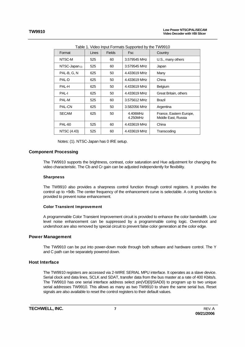
TW9910 supports all common video formats as shown in Table 1. The video decoder needs to be programmed appropriately for each of the composite video input formats.
TW9910
TECHWELL, INC. 7 REV. A 09/21/2006
Low Power NTSC/PAL/SECAM Video Decoder with VBI Slicer
Table 1. Video Input Formats Supported by the TW9910 Format Lines Fields Fsc Country
NTSC-M 525 60 3.579545 MHz U.S., many others
NTSC-Japan (1) 525 60 3.579545 MHz Japan
PAL-B, G, N 625 50 4.433619 MHz Many
PAL-D 625 50 4.433619 MHz China
PAL-H 625 50 4.433619 MHz Belgium
PAL-I 625 50 4.433619 MHz Great Britain, others
PAL-M 525 60 3.575612 MHz Brazil
PAL-CN 625 50 3.582056 MHz Argentina
SECAM 625 50 4.406MHz 4.250MHz
France, Eastern Europe, Middle East, Russia
PAL-60 525 60 4.433619 MHz China
NTSC (4.43) 525 60 4.433619 MHz Transcoding
Notes: (1). NTSC-Japan has 0 IRE setup.
Component Processing
The TW9910 supports the brightness, contrast, color saturation and Hue adjustment for changing the video characteristic. The Cb and Cr gain can be adjusted independently for flexibility.
Sharpness
The TW9910 also provides a sharpness control function through control registers. It provides the control up to +9db. The center frequency of the enhancement curve is selectable. A coring function is provided to prevent noise enhancement.
Color Transient Improvement
A programmable Color Transient Improvement circuit is provided to enhance the color bandwidth. Low level noise enhancement can be suppressed by a programmable coring logic. Overshoot and undershoot are also removed by special circuit to prevent false color generation at the color edge.
Power Management
The TW9910 can be put into power-down mode through both software and hardware control. The Y and C path can be separately powered down.
Host Interface
The TW9910 registers are accessed via 2-WIRE SERIAL MPU interface. It operates as a slave device. Serial clock and data lines, SCLK and SDAT, transfer data from the bus master at a rate of 400 Kbits/s. The TW9910 has one serial interface address select pin(VD[0]/SIAD0) to program up to two unique serial addresses TW9910. This allows as many as two TW9910 to share the same serial bus. Reset signals are also available to reset the control registers to their default values.

TW9910
TECHWELL, INC. 8 REV. A 09/21/2006
Low Power NTSC/PAL/SECAM Video Decoder with VBI Slicer
Down-scaling and Cropping
The TW9910 provides two methods to reduce the amount of output video pixel data, downscaling and cropping. The downscaling provides full video image at lower resolution. Cropping provides only a portion of the video image output. All these mechanisms can be controlled independently to yield maximum flexibility in the output stream.
The TW9910 can independently reduce the output video image size in both horizontal and vertical directions using arbitrary scaling ratios up to 1/16 in each direction. The horizontal scaling employs a dynamic 6-tap 32-phase interpolation filter for luma and a 2-tap 8-phase interpolation filter for chroma. The vertical scaling uses the simple line dropping method. It is recommended to choose integer vertical scaling ratio for best result.
The horizontal scaling factor can be calculated according to following equation:
HSCALE = [HACTIVE / Npixel_desired] * 256
Where: Npixel_desired is the number of output pixels per line and HACTIVE is the programmed number of captured pixels per line.
The vertical scaling factor is determined as
VSCALE = [VACTIVE / Nline_desired] * 256
Where: Nline_desired is the number of active lines output per field and VACTIVE is the programmed number of captured lines per field.
Cropping
Cropping allows only subsection of a video image to be output. The VACTIVE signal can be programmed to indicate the number of active lines to be displayed in a video field, and the HACTIVE signal can be programmed to indicate the number of active pixels to be displayed in a video line. The start of the field or frame in the vertical direction is indicated by the leading edge of VSYNC. The start of the line in the horizontal direction is indicated by the leading edge of the HSYNC. The start of the active lines from vertical sync edge is indicated by the VDELAY register. The start of the active pixels from the horizontal edge is indicated by the HDELAY register. The sizes and location of the active video are determined by HDELAY, HACTIVE, VDELAY, and VACTIVE registers. These registers are 8-bit wide, the lower 8-bits is, respectively, in HDELAY_LO, HACTIVE_LO, VDELAY_LO, and VACTIVE_LO. Their upper 2-bit shares the same register CROP_HI.
In order for the cropping to work properly, the following equation should be satisfied.
HDELAY + HACTIVE < Total number of pixels per line.
VDELAY + VACTIVE < Total number of lines per field
Table 2 shows some popular video formats and its recommended register settings. The CCIR601 format refers to the sampling rate of 13.5 MHz. The SQ format for 60 Hz system refers to the sampling rate of 12.27 MHz, and the SQ format for 50 Hz system refers to the use of sampling rate of 14.75 MHz.

TW9910
TECHWELL, INC. 9 REV. A 09/21/2006
Low Power NTSC/PAL/SECAM Video Decoder with VBI Slicer
Scaling Ratio Format Total Resolution
Output Resolution
HSCALE values
VSCALE (frame)
1:1 NTSC SQ NTSC CCIR601 PAL SQ PAL CCIR601
780x525 858x525 944x625 864x625
640x480 720x480 768x576 720x576
0x0100 0x0100 0x0100 0x0100
0x0100 0x0100 0x0100 0x0100
2:1 (CIF) NTSC SQ NTSC CCIR601 PAL SQ PAL CCIR601
390x262 429x262 472x312 432x312
320x240 360x240 384x288 360x288
0x0200 0x0200 0x0200 0x0200
0x0200 0x0200 0x0200 0x0200
4:1 (QCIF) NTSC SQ NTSC CCIR601 PAL SQ PAL CCIR601
195x131 214x131 236x156 216x156
160x120 180x120 192x144 180x144
0x0400 0x0400 0x0400 0x0400
0x0400 0x0400 0x0400 0x0400
Table 2. HSCALE and VSCALE value for some popular video formats.

TW9910
TECHWELL, INC. 10 REV. A 09/21/2006
Low Power NTSC/PAL/SECAM Video Decoder with VBI Slicer
Output Interface
ITU-R BT.656
ITU-R BT.656 defines strict EAV/SAV Code, video data output timing, H blanking timing, and V Blanking timing. In this mode, VD[15:8] pins are only effective and CLKx2 pin should be used for data clock signal. EAV/SAV Code format is shown as follows. Bit 7 of forth byte in EAV/SAV code must be “1” in ITU-R BT.656 standard. For that reason, VIPCFG Register bit must be set to “1”.
Table3. ITU-R BT.656 SAV and EAV code sequence VD15 VD14 VD13 VD12 VD11 VD10 VD9 VD8
1st byte 1 1 1 1 1 1 1 1 2nd byte 0 0 0 0 0 0 0 0 3rd byte 0 0 0 0 0 0 0 0 4th byte *C F V H V XOR H F XOR H F XOR V F XOR V XOR H
*C is set by VIPCFG register bit.
For complete IRU-R BT.656 standard, following setting is recommended.
Table 4. ITU-R BT.656 Register set up Register 525 line system 625 line system MODE 1 1 LEN 0 0
VDELAY 0x012 0x018 VACTIVE 0X0F4 0x120 HACTIVE 0x2D0 0x2D0 HA_EN 1 1 VIPCFG 1 1
NTSC656 1 0
ITU-R BT.656 for 525-line system has 244 video active lines in odd field and 243 vide active lines in even field. NTSC656 register bit controls this video active line length.
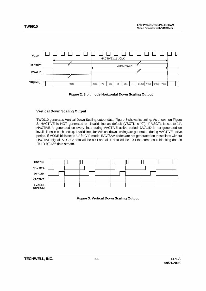
Horizontal Down Scaling Output
TW9910 generates Horizontal down scaling output data. Figure 2 shows 8 bit mode Horizontal Down Scaling output timing. As shown on Figure 2, Horizontal Down Scaled data are generated by continuous data stream. The trailing edge of DVALID signal changes with the trailing edge of HACTIVE signal. Data value from the leading edge of HACTIVE to the leading edge of DVALID is programmable by CNTL656 register. If CNTL656 is set to “1”, all Y and CbCr data will be 0x00. If CNTL656 is set to “0”, all Y data will be 0x10 and all CbCr data will be 0x80. VIP application normally uses 0x00 data as invalid data. Figure 2 shows 360 active pixels output timing after horizontal downscaling.
TW9910
TECHWELL, INC. 11 REV. A 09/21/2006
Low Power NTSC/PAL/SECAM Video Decoder with VBI Slicer
Vertical Down Scaling Output
TW9910 generates Vertical Down Scaling output data. Figure 3 shows its timing. As shown on Figure 3, HACTIVE is NOT generated on invalid line as default (VSCTL is “0”). If VSCTL is set to “1”, HACTIVE is generated on every lines during VACTIVE active period. DVALID is not generated on invalid lines in each setting. Invalid lines for Vertical down scaling are generated during VACTIVE active period. If MODE bit is set to “1” for VIP mode, EAV/SAV codes are not generated on those lines without HACTIVE signal. All CbCr data will be 80H and all Y data will be 10H the same as H-blanking data in ITU-R BT.656 data stream.
VCLKHACTIVE x 2 VCLK
360x2 VCLKHACTIVE
DVALID
Figure 2. 8 bit mode Horizontal Down Scaling Output
... Y359VD[15:8]
Y358 Cr358Cb358Cb0 Cr0Y0 Y1 Cb20x00
HACTIVE
DVALID
Figure 3. Vertical Down Scaling Output
VACTIVE
HSYNC
LVALID(OPTION)

TW9910
TECHWELL, INC. 12 REV. A 09/21/2006
Low Power NTSC/PAL/SECAM Video Decoder with VBI Slicer
VBI Data Processing
Raw VBI data output
TW9910 supports raw VBI data output. Raw VBI data output has the same vertical line delay timing as video output. Horizontal output timing is also programmable by VBIDELAY register. Raw VBI data is generated during HACTIVE active period (from SAV to EAV) as Video data output. Total pixel number of raw VBI data per line is twice as many as HACTIVE register value. If VBI EN register is set to “1”, all vertical blanking output while VACTIVE is inactive will be raw VBI data output. If VVBI registers are set to more than “1”, the VVBI number lines from top video active lines will also be raw VBI data output lines.
VBI Data Slicer
The following VBI standards are supported by VBI Data slicer. The VBI Data slicing is controlled by the registers LCTL6 to LCTL26. Registers LCTL6 to LCTL26 are controlling the slicing process itself. LCTL6 to LCTL26 defines the Data Type to be decoded. The Data Type can be specified on a line by line basis for line6 to line26 and for even and odd field depending on the detected TV system standard. The setting for LCTL26 is valid for the rest of the corresponding field. Normally no text data 0H (video data) should be selected to render the VBI Data slicer inactive during active video. LCTRL26 is useful for Full-Field Teletext mode in the case of NABTS.
NABTS is 525 Teletext-C. Japan’s MOJI is 525 Teletext-D. Didon Antiope is 625 Teletext-A. VBI Data slicer supports up to Physical layer, Link layer in ITU-R BT.653-2. Japan’s EIAJ CPR-1204 shown as 525 WSS has the same physical layer protocol as that of CGMS.
The sliced VBI data is embedded in the ITU-R BT.656 output stream, using the intervals between the End of Active Video (EAV) and the Start of Active Vide(SAV) codes of each line and formatted according to ITU-R BT.1364 Ancillary data packet Type 2.
Table 5. VBI Standard. STANDARD TYPE TV Systems
(lines/freq) Bit Rate (Mbits/s)
Modulation Data Type
625 Teletext-B 625/50 6.9375 NRZ 1H 525 Teletext-B 525/60 5.727272 NRZ 1H 625 Teletext-C 625/50 5.734375 NRZ 2H 525 Teletext-C 525/60 5.727272 NRZ 2H 625 Teletext-D 625/50 5.6427875 NRZ 3H 525 Teletext-D 525/60 5.727272 NRZ 3H 625 CC 625/50 0.500 NRZ 4H 525 CC 525/60 0.503 NRZ 4H 625 WSS 626/50 5 Bi-phase 5H 525 WSS(CGMS) 525/60 0.447443 NRZ 5H 625 VITC 625/50 1.8125 NRZ 6H 525 VITC 525/60 1.7898 NRZ 6H Gemstar 2x 525/60 1.007 NRZ 7H Gemstar 1x 525/60 0.503 NRZ 8H VPS 625/50 5 Bi-phase 9H 625 Teletext-A 625/50 6.203125 NRZ AH

TW9910
TECHWELL, INC. 13 REV. A 09/21/2006
Low Power NTSC/PAL/SECAM Video Decoder with VBI Slicer
Sliced VBI Data output format
After 4 bytes of EAV code, sliced VBI ANC data packets are generated by following format. Byte1 to Byte4N+7 data stream is formatted according to ITU-R BT.1364 ANC data packet type2. BC data byte is optional and not included in ANC data packet type 2 BC data byte is inserted after ANC data packet type2.
Table 6. Sliced VBI ANC data packet BYTE No.
D7 MSB
D6 D5 D4 D3 D2 D1 D0 LSB
DESCRIPTION
1 0 0 0 0 0 0 0 0 Ancillary data flag
2 1 1 1 1 1 1 1 1
3 1 1 1 1 1 1 1 1
4 NEP EP 0 DID4 DID3 DID2 DID1 DID0 DID 5 NEP EP SDID5 SDID4 SDID3 SDID2 SDID1 SDID0 SDID 6 NEP EP DC5 DC4 DC3 DC2 DC1 DC0 DC 7 OP FID LN8 LN7 LN6 LN5 LN4 LN3 IDI1. UDW1 8 OP LN2 LN1 LN0 DT3 DT2 DT1 DT0 IDI2. UDW 2 9 Sliced VBI Data byte 1 Sliced VBI Data No.1. UDW3
10 Sliced VBI Data byte 2 Sliced VBI Data No.2. UDW4 11 Sliced VBI Data byte 3 Sliced VBI Data No.3 UDW5 12 Sliced VBI Data byte 4 Sliced VBI Data No.4. UDW6 13 Sliced VBI Data byte 5 Sliced VBI Data No.5. UDW7 . .
. .
4N+6 Sliced VBI Data byte last or FILLDATA Sliced VBI Data Last or FILLDATA. UDW 4N
4N+7 NCS6 CS6 CS5 CS4 CS3 CS2 CS1 CS0 CS 4N+8 OP 0 BC5 BC4 BC3 BC2 BC1 BC0 BC
1. EP is Even Parity of bits 5 to 0 in same 1 byte. 2. NEP is inverted EP in same 1 byte. 3. {DID4,DID3,DID2,DID1,DID0} is DID register value. 4. {SDID5,SDID4,SDID3,SDID2,SDID1,SDID0} is SDID register value. 5. {DC5,DC4,DC3,DC2,DC1,DC0} is the number of DOWRD data length from UDW1 to UDW4N.On this table,
{DC5,DC4,DC3,DC2,DC1,DC0} is N(decimal). 6. OP is Odd Parity of bits 6 to 0 in same 1 byte. 7. FID=0: odd field ; FID=1: even field. 8. {LN8,LN7,LN6,LN5,LN4,LN3,LN2,LN1,LN0} is the line number of current sliced VBI data. 9. {DT3,DT2,DT1,DT0} is the Data Type shown on Table 10. NCS6 is inverted CS6. 11. {CS6,CS5,CS4,CS3,CS2,CS1,CS0} is the checksum value calculated from DID to UDW4N. 12. UDW1 to UDW4N are the User data words(UDW) shown on ITU-R BT.1364 ANC data packet type 2. 13. [BC5,BC4,BC3,BC2,BC1,BC0] is the number of valid bytes from UDW1 to UDW4N. 14. FILLDATA is FILLDATA register value. FILLDATA is inserted after last valid bytes to make 4N number byte stream sometimes.

TW9910
TECHWELL, INC. 14 REV. A 09/21/2006
Low Power NTSC/PAL/SECAM Video Decoder with VBI Slicer
Following shows various type of ANC data packet to be output
Table 7. Closed Captioning ANC data packet BYTE No.
D7 MSB
D6 D5 D4 D3 D2 D1 D0 LSB
DESCRIPTION
1 0 0 0 0 0 0 0 0 Ancillary data flag
2 1 1 1 1 1 1 1 1
3 1 1 1 1 1 1 1 1
4 NEP EP 0 DID4 DID3 DID2 DID1 DID0 DID 5 NEP EP SDID5 SDID4 SDID3 SDID2 SDID1 SDID0 SDID 6 0 1 0 0 0 0 0 1 DC 7 OP FID LN8 LN7 LN6 LN5 LN4 LN3 IDI1. UDW1 8 OP LN2 LN1 LN0 0 1 0 0 IDI2. UDW 2 9 1st Character byte UDW3
10 2nd Character byte UDW4 11 NCS6 CS6 CS5 CS4 CS3 CS2 CS1 CS0 CS
12 0 0 0 0 0 1 0 0 BC
Table 8. CGMS ANC data packet BYTE No.
D7 MSB
D6 D5 D4 D3 D2 D1 D0 LSB
DESCRIPTION
1 0 0 0 0 0 0 0 0 Ancillary dataflag
2 1 1 1 1 1 1 1 1
3 1 1 1 1 1 1 1 1
4 NEP EP 0 DID4 DID3 DID2 DID1 DID0 DID 5 NEP EP SDID5 SDID4 SDID3 SDID2 SDID1 SDID0 SDID 6 0 1 0 0 0 0 1 0 DC 7 OP FID LN8 LN7 LN6 LN5 LN4 LN3 IDI1. UDW1 8 OP LN2 LN1 LN0 0 1 0 1 IDI2. UDW 2 9 WSS[7:0] UDW3
10 WSS[15:8] UDW4 11 {0H,WSS[19:16]} UDW5 12 CRCERRORCODE UDW6 13 FILLDATA UDW7 14 FILLDATA UDW8 15 NCS6 CS6 CS5 CS4 CS3 CS2 CS1 CS0 CS
16 1 0 0 0 0 1 1 0 BC 1.CRCERRORCODE is optional byte. 41H means “this wss data has CRC Error”. 80H means no CRC error.
Table 9. 625 line Wide Screen signaling ANC data packet BYTE No.
D7 MSB
D6 D5 D4 D3 D2 D1 D0 LSB
DESCRIPTION
1 0 0 0 0 0 0 0 0 Ancillary dataflag
2 1 1 1 1 1 1 1 1
3 1 1 1 1 1 1 1 1
4 NEP EP 0 DID4 DID3 DID2 DID1 DID0 DID 5 NEP EP SDID5 SDID4 SDID3 SDID2 SDID1 SDID0 SDID 6 0 1 0 0 0 0 0 1 DC 7 OP FID LN8 LN7 LN6 LN5 LN4 LN3 IDI1. UDW1 8 OP LN2 LN1 LN0 0 1 0 1 IDI2. UDW 2 9 WSS[7:0] UDW3
10 {00b,WSS[13:8] UDW4

TW9910
TECHWELL, INC. 15 REV. A 09/21/2006
Low Power NTSC/PAL/SECAM Video Decoder with VBI Slicer
12 NCS6 CS6 CS5 CS4 CS3 CS2 CS1 CS0 CS
13 0 0 0 0 0 1 0 0 BC
Table 10. 625 Teletext-A ANC data packet BYTE No.
D7 MSB
D6 D5 D4 D3 D2 D1 D0 LSB
DESCRIPTION
1 0 0 0 0 0 0 0 0 Ancillary dataflag
2 1 1 1 1 1 1 1 1
3 1 1 1 1 1 1 1 1
4 NEP EP 0 DID4 DID3 DID2 DID1 DID0 DID 5 NEP EP SDID5 SDID4 SDID3 SDID2 SDID1 SDID0 SDID 6 0 1 0 0 1 0 1 1 DC 7 OP FID LN8 LN7 LN6 LN5 LN4 LN3 IDI1. UDW1 8 OP LN2 LN1 LN0 1 0 1 0 IDI2. UDW 2 9 FRAME CDDE UDW3
10 BYTE4 UDW4 11 BYTE5 UDW5 . . . .
46 BYTE40 UDW40 47 HAMM84ERROR UDW41 48 FILLDATA UDW42 49 FILLDATA UDW43 50 FILLDATA UDW44 51 NCS6 CS6 CS5 CS4 CS3 CS2 CS1 CS0 CS
52 0 0 1 0 1 0 0 1 BC 1. FRAME CODE is E7H if it’s received correctly. 2. HAMM84ERROR is 41H if more than 1 8/4 Hamming code error in this packet,80H means no 8/4 Hamming error.
Table 11. 625 Teletext-B ANC data packet BYTE No.
D7 MSB
D6 D5 D4 D3 D2 D1 D0 LSB
DESCRIPTION
1 0 0 0 0 0 0 0 0 Ancillary dataflag
2 1 1 1 1 1 1 1 1
3 1 1 1 1 1 1 1 1
4 NEP EP 0 DID4 DID3 DID2 DID1 DID0 DID 5 NEP EP SDID5 SDID4 SDID3 SDID2 SDID1 SDID0 SDID 6 1 0 0 0 1 1 0 0 DC 7 OP FID LN8 LN7 LN6 LN5 LN4 LN3 IDI1. UDW1 8 OP LN2 LN1 LN0 0 0 0 1 IDI2. UDW 2 9 FRAME CDDE UDW3
10 BYTE4 UDW4 11 BYTE5 UDW5 . . . .
50 BYTE44 UDW44 51 BYTE45 UDW45 52 HAMM84ERROR UDW46 53 FILLDATA UDW47 54 FILLDATA UDW48 55 NCS6 CS6 CS5 CS4 CS3 CS2 CS1 CS0 CS
56 1 0 1 0 1 1 1 0 BC 1.FRAME CODE is 27H if it’s received correctly. 2.HAMM84ERROR is 41H if more than 1 8/4 Hamming code error in this packet,80H means no 8/4 Hamming error.

TW9910
TECHWELL, INC. 16 REV. A 09/21/2006
Low Power NTSC/PAL/SECAM Video Decoder with VBI Slicer
Table 12. 525 Teletext-B ANC data packet BYTE No.
D7 MSB
D6 D5 D4 D3 D2 D1 D0 LSB
DESCRIPTION
1 0 0 0 0 0 0 0 0 Ancillary dataflag
2 1 1 1 1 1 1 1 1
3 1 1 1 1 1 1 1 1
4 NEP EP 0 DID4 DID3 DID2 DID1 DID0 DID 5 NEP EP SDID5 SDID4 SDID3 SDID2 SDID1 SDID0 SDID 6 1 0 0 0 1 0 1 0 DC 7 OP FID LN8 LN7 LN6 LN5 LN4 LN3 IDI1. UDW1 8 OP LN2 LN1 LN0 0 0 0 1 IDI2. UDW 2 9 FRAME CDDE UDW3
10 BYTE4 UDW4 11 BYTE5 UDW5 . . . .
30 BYTE36 UDW36 31 BYTE37 UDW37 32 HAMM84ERROR UDW38 33 FILLDATA UDW39 34 FILLDATA UDW40 35 NCS6 CS6 CS5 CS4 CS3 CS2 CS1 CS0 CS
36 1 0 1 0 0 1 1 0 BC
1.FRAME CODE is 27H if it’s received correctly. 2.HAMM84ERROR is 41H if more than 1 8/4 Hamming code error in this packet,80H means no 8/4 Hamming error.
Table 13. 625 Teletext-C and 525 Teletext-C ANC data packet BYTE No.
D7 MSB
D6 D5 D4 D3 D2 D1 D0 LSB
DESCRIPTION
1 0 0 0 0 0 0 0 0 Ancillary dataflag
2 1 1 1 1 1 1 1 1
3 1 1 1 1 1 1 1 1
4 NEP EP 0 DID4 DID3 DID2 DID1 DID0 DID 5 NEP EP SDID5 SDID4 SDID3 SDID2 SDID1 SDID0 SDID 6 1 0 0 0 1 0 1 0 DC 7 OP FID LN8 LN7 LN6 LN5 LN4 LN3 IDI1. UDW1 8 OP LN2 LN1 LN0 0 0 1 0 IDI2. UDW 2 9 FRAME CDDE UDW3
10 BYTE4 UDW4 11 BYTE5 UDW5 . . . .
42 BYTE36 UDW36 43 HAMM84ERROR UDW37 44 FILLDATA UDW38 45 FILLDATA UDW39 46 FILLDATA UDW40 47 NCS6 CS6 CS5 CS4 CS3 CS2 CS1 CS0 CS
48 0 0 1 0 0 1 0 1 BC
1.FRAME CODE is E7H if it’s received correctly. 2.HAMM84ERROR is 41H if more than 1 8/4 Hamming code error in this packet,80H means no 8/4 Hamming error.
TW9910
TECHWELL, INC. 17 REV. A 09/21/2006
Low Power NTSC/PAL/SECAM Video Decoder with VBI Slicer
Table 14. 625 Teletext-D and 525 Teletext-D ANC data packet BYTE No.
D7 MSB
D6 D5 D4 D3 D2 D1 D0 LSB
DESCRIPTION
1 0 0 0 0 0 0 0 0 Ancillary dataflag
2 1 1 1 1 1 1 1 1
3 1 1 1 1 1 1 1 1
4 NEP EP 0 DID4 DID3 DID2 DID1 DID0 DID 5 NEP EP SDID5 SDID4 SDID3 SDID2 SDID1 SDID0 SDID 6 1 0 0 0 1 0 1 0 DC 7 OP FID LN8 LN7 LN6 LN5 LN4 LN3 IDI1. UDW1 8 OP LN2 LN1 LN0 0 0 1 1 IDI2. UDW 2 9 FRAME CDDE UDW3
10 BYTE4 UDW4 11 BYTE5 UDW5 . . . .
42 BYTE36 UDW36 43 BYTE37 UDW37 44 FILLDATA UDW38 45 FILLDATA UDW39 46 FILLDATA UDW40 47 NCS6 CS6 CS5 CS4 CS3 CS2 CS1 CS0 CS
48 0 0 1 0 0 1 0 1 BC
1.FRAME CODE is A7H if it’s received correctly.
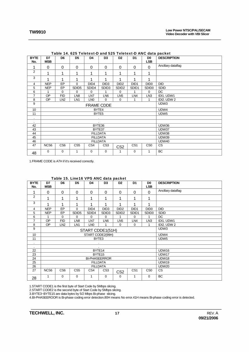
Table 15. Line16 VPS ANC data packet BYTE No.
D7 MSB
D6 D5 D4 D3 D2 D1 D0 LSB
DESCRIPTION
1 0 0 0 0 0 0 0 0 Ancillary dataflag
2 1 1 1 1 1 1 1 1
3 1 1 1 1 1 1 1 1
4 NEP EP 0 DID4 DID3 DID2 DID1 DID0 DID 5 NEP EP SDID5 SDID4 SDID3 SDID2 SDID1 SDID0 SDID 6 1 0 0 0 0 1 0 1 DC 7 OP FID LN8 LN7 LN6 LN5 LN4 LN3 IDI1. UDW1 8 OP LN2 LN1 LN0 1 0 0 1 IDI2. UDW 2 9 START CDDE1(51H) UDW3
10 START CODE2(99H) UDW4 11 BYTE3 UDW5 . . . .
22 BYTE14 UDW16 23 BYTE15 UDW17 24 BI-PHASEERROR UDW18 25 FILLDATA UDW19 26 FILLDATA UDW20 27 NCS6 CS6 CS5 CS4 CS3 CS2 CS1 CS0 CS
28 1 0 0 1 0 0 1 0 BC
1.START CODE1 is the first byte of Start Code by 5Mbps slicing. 2.START CODE2 is the second byte of Start Code by 5Mbps slicing. 3. BYTE3~BYTE15 are data bytes by 5/2 Mbps Bi-phase slicing. 4. BI-PHASEEROOR is Bi-phase coding error detection.80H means No error.41H means Bi-phase coding error is detected.
TW9910
TECHWELL, INC. 18 REV. A 09/21/2006
Low Power NTSC/PAL/SECAM Video Decoder with VBI Slicer
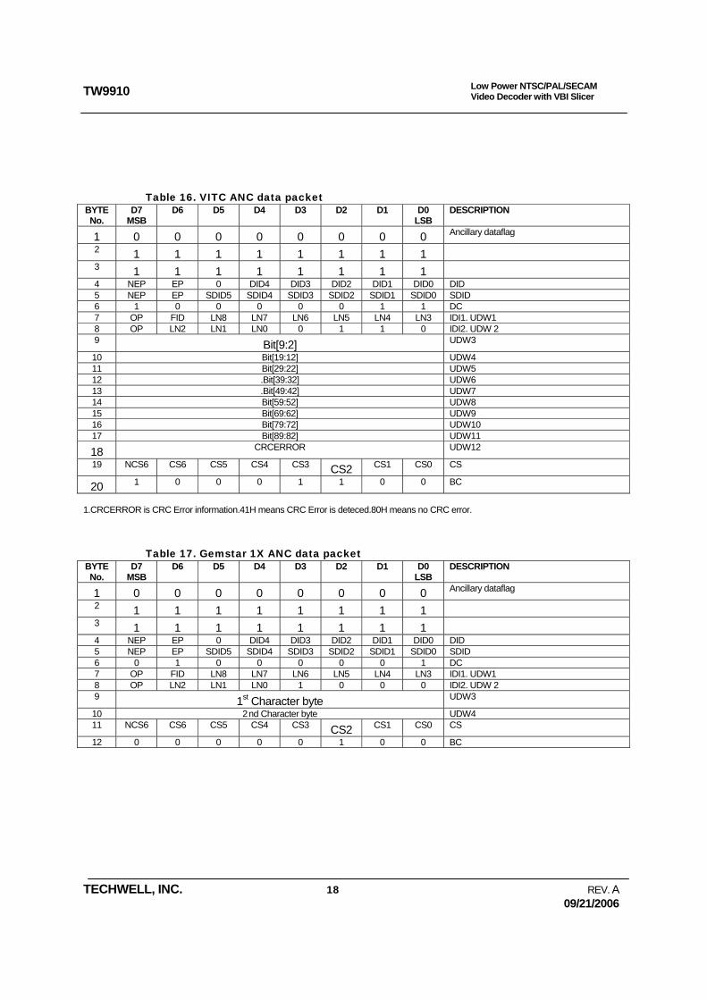
Table 16. VITC ANC data packet BYTE No.
D7 MSB
D6 D5 D4 D3 D2 D1 D0 LSB
DESCRIPTION
1 0 0 0 0 0 0 0 0 Ancillary dataflag
2 1 1 1 1 1 1 1 1
3 1 1 1 1 1 1 1 1
4 NEP EP 0 DID4 DID3 DID2 DID1 DID0 DID 5 NEP EP SDID5 SDID4 SDID3 SDID2 SDID1 SDID0 SDID 6 1 0 0 0 0 0 1 1 DC 7 OP FID LN8 LN7 LN6 LN5 LN4 LN3 IDI1. UDW1 8 OP LN2 LN1 LN0 0 1 1 0 IDI2. UDW 2 9 Bit[9:2] UDW3
10 Bit[19:12] UDW4 11 Bit[29:22] UDW5 12 .Bit[39:32] UDW6 13 .Bit[49:42] UDW7 14 Bit[59:52] UDW8 15 Bit[69:62] UDW9 16 Bit[79:72] UDW10 17 Bit[89:82] UDW11
18 CRCERROR UDW12
19 NCS6 CS6 CS5 CS4 CS3 CS2 CS1 CS0 CS
20 1 0 0 0 1 1 0 0 BC
1.CRCERROR is CRC Error information.41H means CRC Error is deteced.80H means no CRC error.
Table 17. Gemstar 1X ANC data packet BYTE No.
D7 MSB
D6 D5 D4 D3 D2 D1 D0 LSB
DESCRIPTION
1 0 0 0 0 0 0 0 0 Ancillary dataflag
2 1 1 1 1 1 1 1 1
3 1 1 1 1 1 1 1 1
4 NEP EP 0 DID4 DID3 DID2 DID1 DID0 DID 5 NEP EP SDID5 SDID4 SDID3 SDID2 SDID1 SDID0 SDID 6 0 1 0 0 0 0 0 1 DC 7 OP FID LN8 LN7 LN6 LN5 LN4 LN3 IDI1. UDW1 8 OP LN2 LN1 LN0 1 0 0 0 IDI2. UDW 2 9 1st Character byte UDW3
10 2 nd Character byte UDW4 11 NCS6 CS6 CS5 CS4 CS3 CS2 CS1 CS0 CS
12 0 0 0 0 0 1 0 0 BC

TW9910
TECHWELL, INC. 19 REV. A 09/21/2006
Low Power NTSC/PAL/SECAM Video Decoder with VBI Slicer
Table 18. Gemstar 2X ANC data packet BYTE No.
D7 MSB
D6 D5 D4 D3 D2 D1 D0 LSB
DESCRIPTION
1 0 0 0 0 0 0 0 0 Ancillary dataflag
2 1 1 1 1 1 1 1 1
3 1 1 1 1 1 1 1 1
4 NEP EP 0 DID4 DID3 DID2 DID1 DID0 DID 5 NEP EP SDID5 SDID4 SDID3 SDID2 SDID1 SDID0 SDID 6 0 1 0 0 0 0 1 0 DC 7 OP FID LN8 LN7 LN6 LN5 LN4 LN3 IDI1. UDW1 8 OP LN2 LN1 LN0 0 1 1 1 IDI2. UDW 2 9 FRAMECODE1 UDW3
10 FRAMECODE2 UDW4
11 Data Byte 1 UDW5
12 Data Byte 2 UDW6
13 Data Byte 3 UDW7
14 Data Byte 4 UDW8 15 NCS6 CS6 CS5 CS4 CS3 CS2 CS1 CS0 CS
16 0 0 0 0 1 0 0 0 BC 1. FRAMCODE1 is B9H if Frame Code is correctly received. 2. FRAMCODE2 is 05H if Frame Code is correctly received.

TW9910
TECHWELL, INC. 20 REV. A 09/21/2006
Low Power NTSC/PAL/SECAM Video Decoder with VBI Slicer
Two Wire Serial Bus Interface
Figure 4. Definition of the serial bus interface bus start and stop
Figure 5. One complete register read sequence via the serial bus interface
Figure 6. One complete register write sequence via the serial bus interface
SDAT
Start Condition Stop Condition
SCLK
SCLK
Device ID (1-7) R/W Index (1-8) Data (1-8)
SDAT
Start Condition
Stop Condition
AckAck Ack
Re-start Condition
SCLK
Device ID (1-7) R/W Index (1-8)SDAT
Ack Ack
Data (1-8)
Stop Condition Nack
Start Condition
Device ID (1-7) R/W
Ack

TW9910
TECHWELL, INC. 21 REV. A 09/21/2006
Low Power NTSC/PAL/SECAM Video Decoder with VBI Slicer
The two wire serial bus interface is used to allow an external micro-controller to write control data to, and read control or other information from the TW9910 registers. SCLK is the serial clock and SDAT is the data line. Both lines are pulled high by resistors connected to VDD. ICs communicate on the bus by pulling SCLK and SDAT low through open drain outputs. In normal operation the master generates all clock pulses, but control of the SDAT line alternates back and forth between the master and the slave. For both read and write, each byte is transferred MSB first, and the data bit is valid whenever SCLK is high.
The TW9910 is operated as a bus slave device. It can be programmed to respond to one of two 7-bit slave device addresses by tying the SIAD (Serial Interface ADdress) pin ether to VDD or VSS (See Table 19) through a pull-up or pull-down resister. The SIAD pin is multi-purpose pin and must not tied to VDD or VSS directly. If the SIAD pin is tied to VDD, then the least significant bit of the 7-bit address is a “1”. If the SIAD pin is tied to VSS then the least significant bit of the 7-bit address is a “0”. The most significant 6-bits are fixed. The 7-bit address field is concatenated with the read/write control bit to form the first byte transferred during a new transfer. If the read/write control bit is high the next byte will be read from the slave device. If it is low the next byte will be a write to the slave. When a bus master (the host microprocessor) drives SDAT from high to low, while SCLK is high, this is defined to be a start condition (See Figure 4.). All slaves on the bus listen to determine when a start condition has been asserted.
After a start condition, all slave devices listen for the their device addresses. The host then sends a byte consisting of the 7-bit slave device ID and the R/W bit. This is shown in Figure 5. (For the TW9910, the next byte is normally the index to the TW9910 registers and is a write to the TW9910 therefore the first R/W bit is normally low.)
After transmitting the device address and the R/W bit, the master must release the SDAT line while holding SCLK low, and wait for an acknowledgement from the slave. If the address matches the device address of a slave, the slave will respond by driving the SDAT line low to acknowledge the condition. The master will then continue with the next 8-bit transfer. If no device on the bus responds, the master transmits a stop condition and ends the cycle. Notice that a successful transfer always includes nine clock pulses.
To write to the internal register of theTW9910, the master sends another 8-bits of data, the TW9910 loads this to the register pointed by the internal index register. The TW9910 will acknowledge the 8-bit data transfer and automatically increment the index in preparation for the next data. The master can do multiple writes to the TW9910 if they are in ascending sequential order. After each 8-bit transfer the TW9910 will acknowledge the receipt of the 8-bits with an acknowledge pulse. To end all transfers to the TW9910 the host will issue a stop condition.
Serial Bus Interface 7-bit Slave Address Read/Write bit
1 0 0 0 1 0 SIAD0 1=Read 0=Write
Table 19 TW9910 serial bus interface 7-bit slave address and read write bit
A TW9910 read cycle has two phases. The first phase is a write to the internal index register. The second phase is the read from the data register. (See figure 5). The host initiates the first phase by sending the start condition. It then sends the slave device ID together with a 0 in the R/W bit position. The index is then sent followed by either a stop condition or a second start condition. The second phase starts with the second start condition. The master then resends the same slave device ID with a 1 in the R/W bit position to indicate a read. The slave will transfer the contents of the desired register. The master remains in control of the clock. After transferring eight bits, the slave releases and the master takes control of the SDAT line and acknowledges the receipt of data to the slave. To terminate

TW9910
TECHWELL, INC. 22 REV. A 09/21/2006
Low Power NTSC/PAL/SECAM Video Decoder with VBI Slicer
the last transfer the master will issue a negative acknowledge (SDAT is left high during a clock pulse) and issue a stop condition.
Test Modes
The input pin TMODE combining with RESET# provide different test modes selection. If this pin is low at the rising edge of the RESET# pin and remaining low afterwards, TW9910 is in the normal operating mode. Other test modes can be obtained as shown in Table 20.
Table 20. Test mode selection and description Test mode TMODE
before RESET#
rising edge
TMODE after
RESET# rising edge
Description
Normal 0 0 Normal operation mode.
Pin tri-state 0 1 In this mode, all pin output drivers are tri-stated. Pin leakage current parameters can be measured.
Outputs high 1 0 In this mode, all pin output drivers are forced to the high output state. Pin output high voltage, VOH and IOH, can be measured.
Outputs low 1 1 In this mode, all pin output drivers are forced to the low output state. Pin output low voltage, VOL and IOL, can be measured.

TW9910
TECHWELL, INC. 23 REV. A 09/21/2006
Low Power NTSC/PAL/SECAM Video Decoder with VBI Slicer
Filter Curves
Anti-alias filter
Decimation filter
0 2 4 6 8 10 12
x 106
-50
-45
-40
-35
-30
-25
-20
-15
-10
-5
0
Frequency (Hertz)
Magnitude Response (dB)
0 2 4 6 8 10 12 14 16 18 20-40
-35
-30
-25
-20
-15
-10
-5
0
5
Frequency (Hertz)
Gain (dB)

TW9910
TECHWELL, INC. 24 REV. A 09/21/2006
Low Power NTSC/PAL/SECAM Video Decoder with VBI Slicer
Chroma Band Pass Filter Curves
Luma Notch Filter Curve for NTSC and PAL/SECAM
0 1 2 3 4 5 6 7 8 9
x 106
-50
-45
-40
-35
-30
-25
-20
-15
-10
-5
0
Frequency (Hertz)
Magnitude Response (dB)
0 1 2 3 4 5 6 7 8 9
x 106
-80
-70
-60
-50
-40
-30
-20
-10
0
Frequency (Hertz)
Magnitude Response (dB)
PAL/SEAM
NTSC
PAL/SECAM
NTSC

TW9910
TECHWELL, INC. 25 REV. A 09/21/2006
Low Power NTSC/PAL/SECAM Video Decoder with VBI Slicer
Chrominance Low-Pass Filter Curve
Horizontal Scaler Pre- Filter curves
0 0.05 0.1 0.15 0.2 0.25 0.3 0.35 0.4 0.45 0.5-40
-35
-30
-25
-20
-15
-10
-5
0
Fsig/Fsample
Magnitude Response (dB)
0 0.5 1 1.5 2 2.5 3 3.5 4 4.5 5
x 106
-50
-45
-40
-35
-30
-25
-20
-15
-10
-5
0
Frequency (Hertz)
Magnitude Response (dB)
Low Med
High
HFLT[1:0]=1
HFLT[1:0]=2
HFLT[1:0]=3

TW9910
TECHWELL, INC. 26 REV. A 09/21/2006
Low Power NTSC/PAL/SECAM Video Decoder with VBI Slicer
Peaking Filter Curves
NTSC
PAL
0 1 2 3 4 5 6 7
x 106
0
2
4
6
8
10
12
14
16
Frequency (Hertz)
Magnitude Response (dB)
0 1 2 3 4 5 6 7 8 9
x 106
0
2
4
6
8
10
12
14
16
Frequency (Hertz)
Magnitude Response (dB)

TW9910
TECHWELL, INC. 27 REV. A 09/21/2006
Low Power NTSC/PAL/SECAM Video Decoder with VBI Slicer
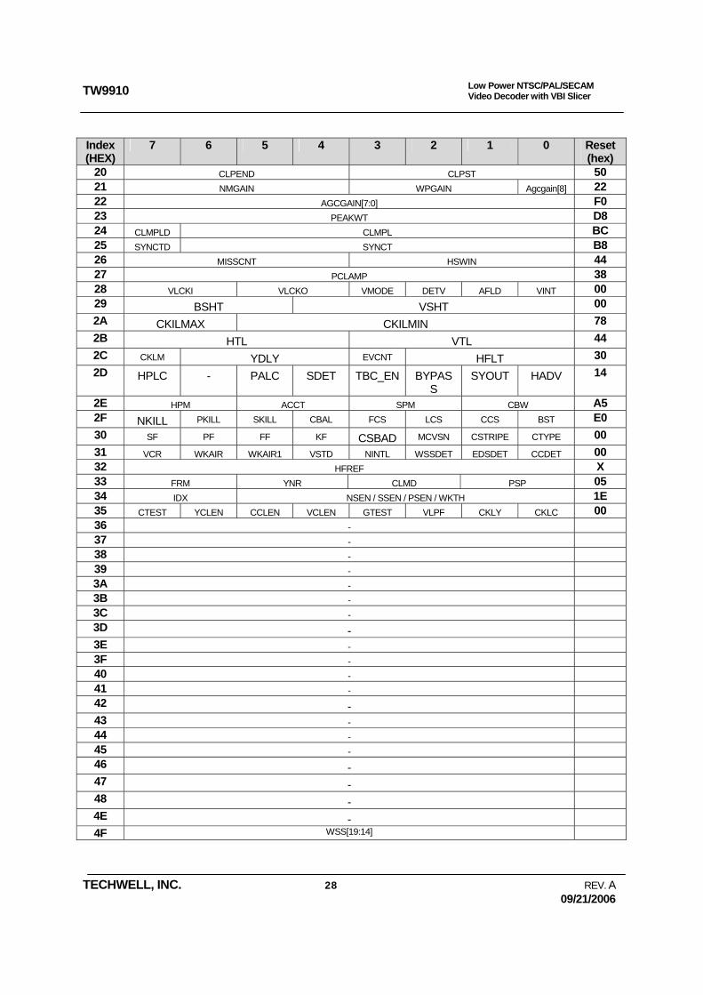
Control Register
TW9910 Register SUMMARY
Index (HEX)
7 6 5 4 3 2 1 0 Reset (hex)
00 ID REV 58 01 VDLOSS HLOCK SLOCK FIELD VLOCK - MONO DET50 00 02 YSEL2 FC27 IFSEL YSEL CSEL SEL 40 03 MODE LEN LLCMODE AINC VSCTL OEN TRI_SEL 04 04 GMEN CKHY HSDLY 00 05 VSP VSSL HSP HSSL 00 06 SRESET IREF VREF AGC_EN CLKPDN Y_PDN C_PDN - 00 07 VDELAY_HI VACTIVE_HI HDELAY_HI HACTIVE_HI 02 08 VDELAY_LO 12 09 VACTIVE_LO F0 0A HDELAY_LO 0F 0B HACTIVE_LO D0 0C PBW DEM PALSW SET7 COMB HCOMP YCOMB PDLY CC 0D VSCALE_LO 00 0E VSCALE_HI HSCALE_HI 11 0F HSCALE_LO 00 10 BRIGHTNESS 00 11 CONTRAST 5C 12 SCURVE - CTI SHARPNESS 11 13 SAT_U 80 14 SAT_V 80 15 HUE 00 16 - - 00 17 SHCOR - VSHP 80 18 CTCOR CCOR VCOR CIF 44 19 VBI_EN VBI_BYT VBI_FRAM HA_EN CTL656 RTSEL 58 1A LLCTEST PLL_PDN - - YFLEN YSV CFLEN CSV 00 1B CK2S CK1S - - 00 1C DTSTUS STDNOW ATREG STANDARD 07 1D START PAL60 PALCN PALM NTSC4 SECAM PALB NTSC 7F 1E - 00 1F TEST 00
TW9910
TECHWELL, INC. 28 REV. A 09/21/2006
Low Power NTSC/PAL/SECAM Video Decoder with VBI Slicer
Index (HEX)
7 6 5 4 3 2 1 0 Reset (hex)
20 CLPEND CLPST 50 21 NMGAIN WPGAIN Agcgain[8] 22 22 AGCGAIN[7:0] F0 23 PEAKWT D8 24 CLMPLD CLMPL BC 25 SYNCTD SYNCT B8 26 MISSCNT HSWIN 44 27 PCLAMP 38 28 VLCKI VLCKO VMODE DETV AFLD VINT 00 29 BSHT VSHT 00 2A CKILMAX CKILMIN 78 2B HTL VTL 44 2C CKLM YDLY EVCNT HFLT 30 2D HPLC - PALC SDET TBC_EN BYPAS
S SYOUT HADV 14
2E HPM ACCT SPM CBW A5 2F NKILL PKILL SKILL CBAL FCS LCS CCS BST E0 30 SF PF FF KF CSBAD MCVSN CSTRIPE CTYPE 00 31 VCR WKAIR WKAIR1 VSTD NINTL WSSDET EDSDET CCDET 00 32 HFREF X 33 FRM YNR CLMD PSP 05 34 IDX NSEN / SSEN / PSEN / WKTH 1E 35 CTEST YCLEN CCLEN VCLEN GTEST VLPF CKLY CKLC 00 36 - 37 - 38 - 39 - 3A - 3B - 3C - 3D - 3E - 3F - 40 - 41 - 42 - 43 - 44 - 45 - 46 - 47 - 48 - 4E - 4F WSS[19:14]
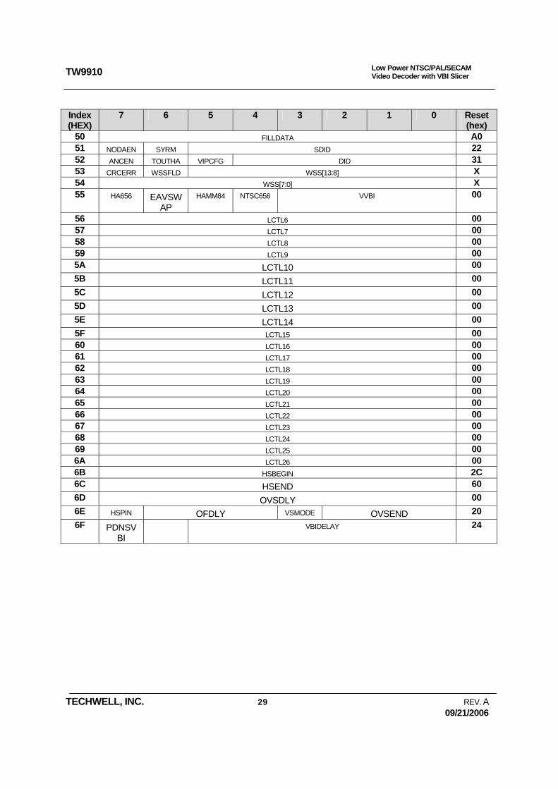
TW9910
TECHWELL, INC. 29 REV. A 09/21/2006
Low Power NTSC/PAL/SECAM Video Decoder with VBI Slicer
Index (HEX)
7 6 5 4 3 2 1 0 Reset (hex)
50 FILLDATA A0 51 NODAEN SYRM SDID 22 52 ANCEN TOUTHA VIPCFG DID 31 53 CRCERR WSSFLD WSS[13:8] X 54 WSS[7:0] X 55 HA656 EAVSW
AP HAMM84 NTSC656 VVBI 00
56 LCTL6 00 57 LCTL7 00 58 LCTL8 00 59 LCTL9 00 5A LCTL10 00 5B LCTL11 00 5C LCTL12 00 5D LCTL13 00 5E LCTL14 00 5F LCTL15 00 60 LCTL16 00 61 LCTL17 00 62 LCTL18 00 63 LCTL19 00 64 LCTL20 00 65 LCTL21 00 66 LCTL22 00 67 LCTL23 00 68 LCTL24 00 69 LCTL25 00 6A LCTL26 00 6B HSBEGIN 2C 6C HSEND 60 6D OVSDLY 00 6E HSPIN OFDLY VSMODE OVSEND 20 6F PDNSV
BI VBIDELAY 24
TW9910
TECHWELL, INC. 30 REV. A 09/21/2006
Low Power NTSC/PAL/SECAM Video Decoder with VBI Slicer
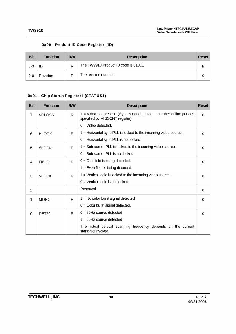
0x00 – Product ID Code Register (ID)
Bit Function R/W Description Reset
7-3 ID R The TW9910 Product ID code is 01011. B
2-0 Revision R The revision number. 0
0x01 – Chip Status Register I (STATUS1)
Bit Function R/W Description Reset
7 VDLOSS R 1 = Video not present. (Sync is not detected in number of line periods specified by MISSCNT register)
0 = Video detected.
0
6 HLOCK R 1 = Horizontal sync PLL is locked to the incoming video source.
0 = Horizontal sync PLL is not locked. 0
5 SLOCK R 1 = Sub-carrier PLL is locked to the incoming video source.
0 = Sub-carrier PLL is not locked. 0
4 FIELD R 0 = Odd field is being decoded.
1 = Even field is being decoded. 0
3 VLOCK R 1 = Vertical logic is locked to the incoming video source.
0 = Vertical logic is not locked. 0
2 Reserved 0
1 MONO R 1 = No color burst signal detected.
0 = Color burst signal detected. 0
0 DET50 R 0 = 60Hz source detected
1 = 50Hz source detected
The actual vertical scanning frequency depends on the current standard invoked.
0

TW9910
TECHWELL, INC. 31 REV. A 09/21/2006
Low Power NTSC/PAL/SECAM Video Decoder with VBI Slicer
0x02 – Input Format (INFORM)
Bit Function R/W Description Reset
7 R/W Reserved. 0
6 FC27 R/W 1 = Input crystal clock frequency is 27MHz.
0 = Square pixel mode. Must use 24.54MHz for 60Hz field rate source or 29.5MHz for 50Hz field rate source.
1
5-4 IFSEL R/W 01 = S-video decoding
00 = Composite video decoding 0
3-2 YSEL R/W These two bits control the Y input video selection.
00 = Mux0 selected
01 = Mux1 selected
10 = Mux2 selected
11 = Mux3 selected
0
1 R/W Reserved 0
0 R/W Reserved 0
TW9910
TECHWELL, INC. 32 REV. A 09/21/2006
Low Power NTSC/PAL/SECAM Video Decoder with VBI Slicer
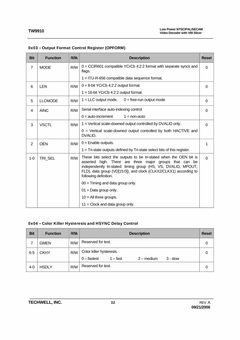
0x03 – Output Format Control Register (OPFORM)
Bit Function R/W Description Reset
7 MODE R/W 0 = CCIR601 compatible YCrCb 4:2:2 format with separate syncs and flags.
1 = ITU-R-656 compatible data sequence format.
0
6 LEN R/W 0 = 8-bit YCrCb 4:2:2 output format.
1 = 16-bit YCrCb 4:2:2 output format. 0
5 LLCMODE R/W 1 = LLC output mode. 0 = free-run output mode 0
4 AINC R/W Serial interface auto-indexing control
0 = auto-increment 1 = non-auto 0
3 VSCTL R/W 1 = Vertical scale-downed output controlled by DVALID only.
0 = Vertical scale-downed output controlled by both HACTIVE and DVALID.
0
2 OEN R/W 0 = Enable outputs.
1 = Tri-state outputs defined by Tri-state select bits of this register. 1
1-0 TRI_SEL R/W These bits select the outputs to be tri-stated when the OEN bit is asserted high. There are three major groups that can be independently tri-stated: timing group (HS, VS, DVALID, MPOUT, FLD), data group (VD[15:0]), and clock (CLKX2/CLKX1) according to following definition.
00 = Timing and data group only.
01 = Data group only.
10 = All three groups.
11 = Clock and data group only.
0
0x04 – Color Killer Hysteresis and HSYNC Delay Control
Bit Function R/W Description Reset
7 GMEN R/W Reserved for test. 0
6-5 CKHY R/W Color killer hysteresis.
0 – fastest 1 – fast 2 – medium 3 - slow 0
4-0 HSDLY R/W Reserved for test. 0
TW9910
TECHWELL, INC. 33 REV. A 09/21/2006
Low Power NTSC/PAL/SECAM Video Decoder with VBI Slicer
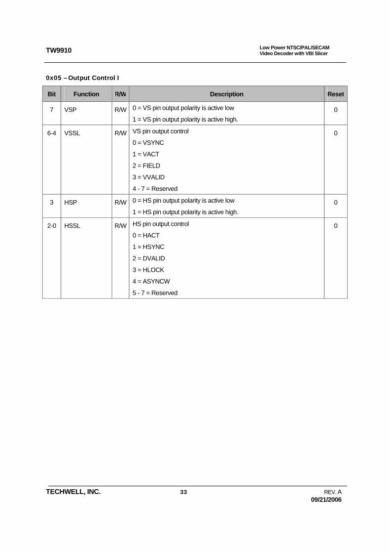
0x05 – Output Control I
Bit Function R/W Description Reset
7 VSP R/W 0 = VS pin output polarity is active low
1 = VS pin output polarity is active high. 0
6-4 VSSL R/W VS pin output control
0 = VSYNC
1 = VACT
2 = FIELD
3 = VVALID
4 - 7 = Reserved
0
3 HSP R/W 0 = HS pin output polarity is active low
1 = HS pin output polarity is active high. 0
2-0 HSSL R/W HS pin output control
0 = HACT
1 = HSYNC
2 = DVALID
3 = HLOCK
4 = ASYNCW
5 - 7 = Reserved
0

TW9910
TECHWELL, INC. 34 REV. A 09/21/2006
Low Power NTSC/PAL/SECAM Video Decoder with VBI Slicer
0x06 – Analog Control Register (ACNTL)
Bit Function R/W Description Reset
7 SRESET W An 1 written to this bit resets the device to its default state but all register content remain unchanged. This bit is self-resetting.
0
6 IREF R/W 0 = Internal current reference 1.
1 = Internal current reference 2. 0
5 VREF R/W 1 = Internal voltage reference.
0 = Internal voltage reference shut down. 0
4 AGC_EN R/W 0 = AGC loop function enabled.
1 = AGC loop function disabled. Gain is set to by AGCGAIN. 0
3 CLK_PDN R/W 0 = Normal clock operation.
1 = System clock in power down mode, but the MPU INTERFACE module and output clocks (CLKX1 and CLKX2) are still active.
0
2 Y_PDN R/W 0 = Luma ADC in normal operation.
1 = Luma ADC in power down mode. 0
1 C_PDN R/W 0 = Chroma ADC in normal operation.
1 = Chroma ADC in power down mode. 0
0 R/W Reserved for future use 0
0x07 – Cropping Register, High (CROP_HI)
Bit Function R/W Description Reset
7-6 VDELAY_HI R/W These bits are bit 9 to 8 of the 10-bit Vertical Delay register. 0
5-4 VACTIVE_HI R/W These bits are bit 9 to 8 of the 10-bit VACTIVE register. Refer to description on Reg09 for its shadow register.
0
3-2 HDELAY_HI R/W These bits are bit 9 to 8 of the 10-bit Horizontal Delay register. 0
1-0 HACTIVE_HI R/W These bits are bit 9 to 8 of the 10-bit HACTIVE register. 2

TW9910
TECHWELL, INC. 35 REV. A 09/21/2006
Low Power NTSC/PAL/SECAM Video Decoder with VBI Slicer
0x08 – Vertical Delay Register, Low (VDELAY_LO)
Bit Function R/W Description Reset
7-0 VDELAY_LO R/W These bits are bit 7 to 0 of the 10-bit Vertical Delay register. The two MSBs are in the CROP_HI register. It defines the number of lines between the leading edge of VSYNC and the start of the active video.
12
0x09 – Vertical Active Register, Low (VACTIVE_LO)
Bit Function R/W Description Reset
7-0 VACTIVE_LO R/W These bits are bit 7 to 0 of the 10-bit Vertical Active register. The two MSBs are in the CROP_HI register. It defines the number of active video lines per frame output.
The VACTIVE register has a shadow register for use with 50Hz source when Atreg of Reg0x1C is not set. This register can be accessed through the same index address by first changing the format standard to any 50Hz standard.
F0
0x0A – Horizontal Delay Register, Low (HDELAY_LO)
Bit Function R/W Description Reset
7-0 HDELAY_LO R/W These bits are bit 7 to 0 of the 10-bit Horizontal Delay register. The two MSBs are in the CROP_HI register. It defines the number of pixels between the leading edge of the HSYNC and the start of the image cropping for active video.
The HDELAY_LO register has two shadow registers for use with PAL and SECAM sources respectively. These register can be accessed using the same index address by first changing the decoding format to the corresponding standard.
0F
0x0B – Horizontal Active Register, Low (HACTIVE_LO)
Bit Function R/W Description Reset
7-0 HACTIVE_LO R/W These bits are bit 7 to 0 of the 10-bit Horizontal Active register. The two MSBs are in the CROP_HI register. It defines the number of active pixels per line output.
D0

TW9910
TECHWELL, INC. 36 REV. A 09/21/2006
Low Power NTSC/PAL/SECAM Video Decoder with VBI Slicer
0x0C – Control Register I (CNTRL1)
Bit Function R/W Description Reset
7 PBW R/W 1 = Wide Chroma BPF BW
0 = Normal Chroma BPF BW 1
6 DEM R/W Secam control
1 = reduction 0 = normal 1
5 PALSW R/W 1 = PAL switch sensitivity low.
0 = PAL switch sensitivity normal. 0
4 SET7 R/W 1 = The black level is 7.5 IRE above the blank level.
0 = The black level is the same as the blank level. 0
3 COMB R/W 1 = Adaptive comb filter on for NTSC
0 = Notch filter 1
2 HCOMP R/W 1 = operation mode 1. (Recommended)
0 = mode 0. 1
1 YCOMB R/W This bit controls the no color burst output behavior.
1 = No comb
0 = comb.
0
0 PDLY R/W PAL delay line control
1 = disable. 0 = enable. 0
0x0D – Vertical Scaling Register, Low (VSCALE_LO)
Bit Function R/W Description Reset
7-0 VSCALE_LO R/W These bits are bit 7 to 0 of the 12-bit vertical scaling ratio register 00h
0x0E – Scaling Register, High (SCALE_HI)
Bit Function R/W Description Reset
7-4 VSCALE_HI R/W These bits are bit 11 to 8 of the 12-bit vertical scaling ratio register. 1
3-0 HSCALE_HI R/W These bits are bit 11 to 8 of the 12-bit horizontal scaling ratio register. 1
TW9910
TECHWELL, INC. 37 REV. A 09/21/2006
Low Power NTSC/PAL/SECAM Video Decoder with VBI Slicer
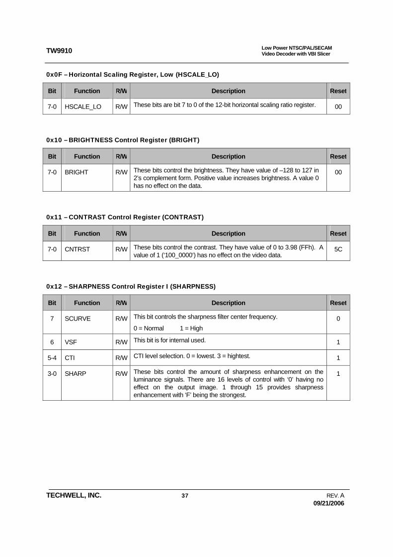
0x0F – Horizontal Scaling Register, Low (HSCALE_LO)
Bit Function R/W Description Reset
7-0 HSCALE_LO R/W These bits are bit 7 to 0 of the 12-bit horizontal scaling ratio register. 00
0x10 – BRIGHTNESS Control Register (BRIGHT)
Bit Function R/W Description Reset
7-0 BRIGHT R/W These bits control the brightness. They have value of –128 to 127 in 2’s complement form. Positive value increases brightness. A value 0 has no effect on the data.
00
0x11 – CONTRAST Control Register (CONTRAST)
Bit Function R/W Description Reset
7-0 CNTRST R/W These bits control the contrast. They have value of 0 to 3.98 (FFh). A value of 1 (‘100_0000‘) has no effect on the video data.
5C
0x12 – SHARPNESS Control Register I (SHARPNESS)
Bit Function R/W Description Reset
7 SCURVE R/W This bit controls the sharpness filter center frequency.
0 = Normal 1 = High 0
6 VSF R/W This bit is for internal used. 1
5-4 CTI R/W CTI level selection. 0 = lowest. 3 = hightest. 1
3-0 SHARP R/W These bits control the amount of sharpness enhancement on the luminance signals. There are 16 levels of control with ‘0’ having no effect on the output image. 1 through 15 provides sharpness enhancement with ‘F’ being the strongest.
1

TW9910
TECHWELL, INC. 38 REV. A 09/21/2006
Low Power NTSC/PAL/SECAM Video Decoder with VBI Slicer
0x13 – Chroma (U) Gain Register (SAT_U)
Bit Function R/W Description Reset
7-0 SAT_U R/W These bits control the digital gain adjustment to the U (or Cb) component of the digital video signal. The color saturation can be adjusted by adjusting the U and V color gain components by the same amount in the normal situation. The U and V can also be adjusted independently to provide greater flexibility. The range of adjustment is 0 to 200%.
80
0x14 – Chroma (V) Gain Register (SAT_V)
Bit Function R/W Description Reset
7-0 SAT_V R/W These bits control the digital gain adjustment to the V (or Cr) component of the digital video signal. The color saturation can be adjusted by adjusting the U and V color gain components by the same amount in the normal situation. The U and V can also be adjusted independently to provide greater flexibility. The range of adjustment is 0 to 200%.
80
0x15 – Hue Control Register (HUE)
Bit Function R/W Description Reset
7-0 HUE R/W These bits control the color hue as 2’s complement number. They have value from +36o (7Fh) to -36o (80h) with an increment of 0.28o. The positive value gives greenish tone and negative value gives purplish tone. The default value is 0o (00h). This is effective only on NTSC system.
00
0x16 – Reserved
Bit Function R/W Description Reset
7-4 R/W Reserved for future use. 0
3-0 R/W Reserved for future use. 0

TW9910
TECHWELL, INC. 39 REV. A 09/21/2006
Low Power NTSC/PAL/SECAM Video Decoder with VBI Slicer
0x17 – Coring
Bit Function R/W Description Reset
7-4 SHCOR R/W These bits provide coring function for the sharpness control. 8
3 Reserved 0
2-0 VSHP R/W Vertical peaking level. 0 = none. 7 = highest. 0
0x18 – Coring and IF compensation (CORING)
Bit Function R/W Description Reset
7-6 CTCOR R/W These bits control the coring for CTI. 1
5-4 CCOR R/W These bits control the low level coring function for the Cb/Cr output. 0
3-2 VCOR R/W These bits control the coring function of vertical peaking. 1
1-0 CIF R/W These bits control the IF compensation level.
0 = None 1 = 1.5dB 2 = 3dB 3 = 6dB 0

TW9910
TECHWELL, INC. 40 REV. A 09/21/2006
Low Power NTSC/PAL/SECAM Video Decoder with VBI Slicer
0x19 – VBI Control Register (VBICNTL)
Bit Function R/W Description Reset
7 VBI_EN R/W 0 = VBI capture disabled.
1 = VBI capture enabled. 0
6 VBI Byte Order R/W If LEN(Reg0x03[6]) is “1”
0 = Pixel 1, 3, 5 … on the VD[15:8] data bus, and pixel 2, 4, 6, … on the VD[7:0] data bus.
1 = Pixel 1, 3, 5, … on the VD[7:0] data bus, and pixel 2, 4, 6, … on the VD[15:8] data bus.
If LEN is “0”
0 = Pixel 2,1,4,3,6,5,…. on the VD[15:8] data bus.
1 = Pixel 1,2,3,4,5,6,…. on the VD[15:8] data bus.
1
5 VBI_ FRAM R/W 0 = Normal mode
1 = ADC output mode
VD[15:8] is Y-ADC data,VD[7:0] pin is C-YADC data
0
4 HA_EN R/W 0 = HACTIVE output is disabled during vertical blanking period.
1 = HACTIVE output is enabled during vertical blanking period. 1
3 CNTL656 R/W 0 = 0x80 and 0x10 code will be output as invalid data during active video line.
1 = 0x00 code will be output as invalid data during active video line.
1
2-0 RTSEL R/W These bits control the real time signal output from the MPOUT pin.
000 = Video loss
001 = H-lock
010 = S-lock
011 = V-lock
100 = MONO
101 = DET50
110 = FIELD
111 = RTCO ( Real Time Control )
0

TW9910
TECHWELL, INC. 41 REV. A 09/21/2006
Low Power NTSC/PAL/SECAM Video Decoder with VBI Slicer
0x1A – Analog Control II
Bit Function R/W Description Reset
7 LLCTEST R/W LLC test mode 0
6 PLL_PDN R/W 0 = LLC PLL in normal operation.
1 = PLL in power down mode. 0
5-4 Reserved 0
3 YFLEN R/W Y-Ch anti-alias filter control
1 = enable 0 = disable 0
2 YSV R/W Y-Ch power saving mode
1 = enable 0 = disable 0
1 CFLEN R/W C-Ch anti-alias filter control
1 = enable 0 = disable 0
0 CSV R/W C-Ch power saving mode
1 = enable 0 = disable 0
0x1B – Output Control II
Bit Function R/W Description Reset
7-6 CK2S R/W CLKX2 pin output control. CK1S[0] together with these two bits (CK1S[0], CK2S) control CLKX2 pin output selection.
000 = VCLK
001 = CLKX1
010 = CLKX2
011 = LLCK
100 = LLCK2
101 = LLCK4
0
5-4 CK1S R/W See CK2S 0
3 R/W Reserved 0
2-0 R/W Reserved 0
TW9910
TECHWELL, INC. 42 REV. A 09/21/2006
Low Power NTSC/PAL/SECAM Video Decoder with VBI Slicer
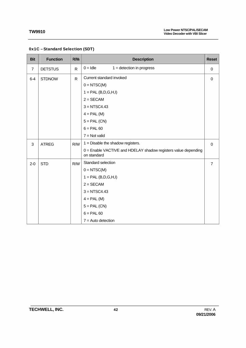
0x1C – Standard Selection (SDT)
Bit Function R/W Description Reset
7 DETSTUS R 0 = Idle 1 = detection in progress 0
6-4 STDNOW R Current standard invoked
0 = NTSC(M)
1 = PAL (B,D,G,H,I)
2 = SECAM
3 = NTSC4.43
4 = PAL (M)
5 = PAL (CN)
6 = PAL 60
7 = Not valid
0
3 ATREG R/W 1 = Disable the shadow registers.
0 = Enable VACTIVE and HDELAY shadow registers value depending on standard
0
2-0 STD R/W Standard selection
0 = NTSC(M)
1 = PAL (B,D,G,H,I)
2 = SECAM
3 = NTSC4.43
4 = PAL (M)
5 = PAL (CN)
6 = PAL 60
7 = Auto detection
7

TW9910
TECHWELL, INC. 43 REV. A 09/21/2006
Low Power NTSC/PAL/SECAM Video Decoder with VBI Slicer
0x1D – Standard Recognition (SDTR)
Bit Function R/W Description Reset
7 ATSTART R/W Writing 1 to this bit will manually initiate the auto format detection process. This bit is a self-resetting bit.
0
6 PAL6_EN R/W 1 = enable recognition of PAL60.
0 = disable recognition. 1
5 PALN_EN R/W 1 = enable recognition of PAL (CN).
0 = disable recognition. 1
4 PALM_EN R/W 1 = enable recognition of PAL (M).
0 = disable recognition. 1
3 NT44_EN R/W 1 = enable recognition of NTSC 4.43.
0 = disable recognition. 1
2 SEC_EN R/W 1 = enable recognition of SECAM.
0 = disable recognition. 1
1 PALB_EN R/W 1 = enable recognition of PAL (B,D,G,H,I).
0 = disable recognition. 1
0 NTSC_EN R/W 1 = enable recognition of NTSC (M).
0 = disable recognition. 1
0x1E – Reserved
Bit Function R/W Description Reset
7-0 R Reserved 0

TW9910
TECHWELL, INC. 44 REV. A 09/21/2006
Low Power NTSC/PAL/SECAM Video Decoder with VBI Slicer
0x1F – Test Control Register (TEST)
Bit Function R/W Description Reset
7-0 TEST R/W This register is reserved for testing purpose. In normal operation, only 0 should be written into this register.
1 = Analog test mode. Y and C channel portion of the device can be tested in this mode. The Y channel ADC output can be obtained from VD[15-8]. The C channel ADC output can be obtained from VD[7-0].
2 = Clamp test mode. Clamp control YU, YUX, YD, YDX, CU, CUX, CD, and CDX are mapped to VD[3-0].
3 = Reserved
4 = Digital test mode1. This is the CVBS test mode. The 8-bit input corresponds to VD[7-0] in the order of bit 7 to 0.
5 = Digital test mode 2. This is the Y/C test mode. Y input is defined by test mode 1. The C channel data is inputted from VD[7-0]. In this mode, only 8/10-bit output format is allowed.
6 = Reserved
7 = Reserved
8 = Reserved
9 = Sync output mode. The 6-bit Sync output corresponds to VD[5-0] in the order of bit 5 to 0. Y and Cb/Cr outputs correspond to VD[15-8] in 422 format
0
TW9910
TECHWELL, INC. 45 REV. A 09/21/2006
Low Power NTSC/PAL/SECAM Video Decoder with VBI Slicer
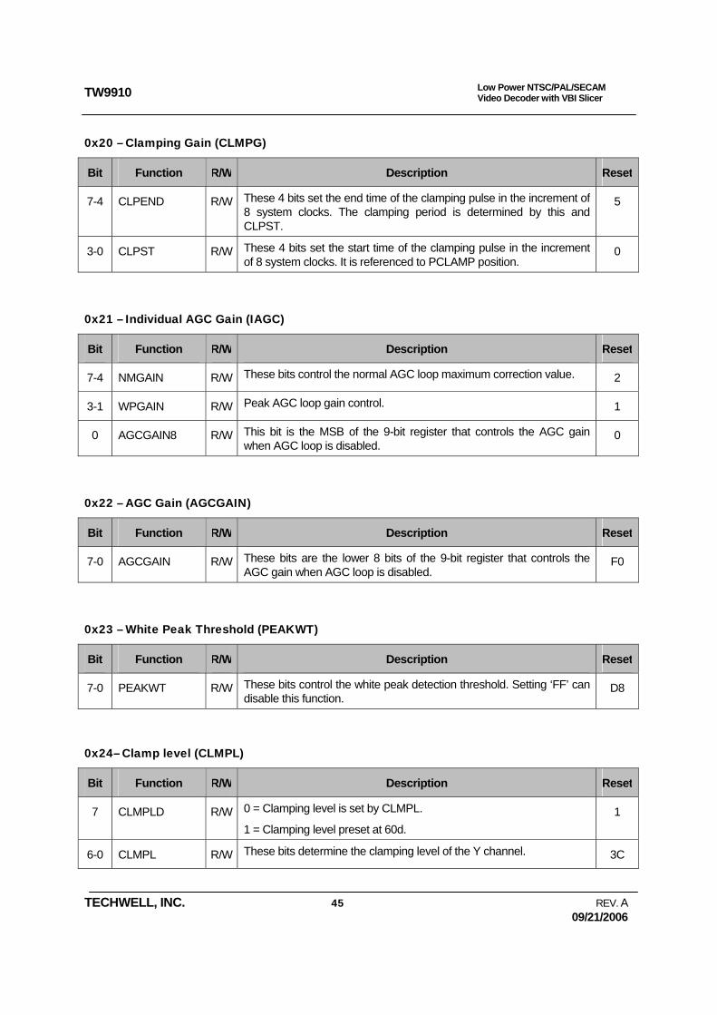
0x20 – Clamping Gain (CLMPG)
Bit Function R/W Description Reset
7-4 CLPEND R/W These 4 bits set the end time of the clamping pulse in the increment of 8 system clocks. The clamping period is determined by this and CLPST.
5
3-0 CLPST R/W These 4 bits set the start time of the clamping pulse in the increment of 8 system clocks. It is referenced to PCLAMP position.
0
0x21 – Individual AGC Gain (IAGC)
Bit Function R/W Description Reset
7-4 NMGAIN R/W These bits control the normal AGC loop maximum correction value. 2
3-1 WPGAIN R/W Peak AGC loop gain control. 1
0 AGCGAIN8 R/W This bit is the MSB of the 9-bit register that controls the AGC gain when AGC loop is disabled.
0
0x22 – AGC Gain (AGCGAIN)
Bit Function R/W Description Reset
7-0 AGCGAIN R/W These bits are the lower 8 bits of the 9-bit register that controls the AGC gain when AGC loop is disabled.
F0
0x23 – White Peak Threshold (PEAKWT)
Bit Function R/W Description Reset
7-0 PEAKWT R/W These bits control the white peak detection threshold. Setting ‘FF’ can disable this function.
D8
0x24– Clamp level (CLMPL)
Bit Function R/W Description Reset
7 CLMPLD R/W 0 = Clamping level is set by CLMPL.
1 = Clamping level preset at 60d. 1
6-0 CLMPL R/W These bits determine the clamping level of the Y channel. 3C

TW9910
TECHWELL, INC. 46 REV. A 09/21/2006
Low Power NTSC/PAL/SECAM Video Decoder with VBI Slicer
0x25– Sync Amplitude (SYNCT)
Bit Function R/W Description Reset
7 SYNCTD R/W 0 = Reference sync amplitude is set by SYNCT.
1 = Reference sync amplitude is preset to 38h. 1
6-0 SYNCT R/W These bits determine the standard sync pulse amplitude for AGC reference.
38
0x26 – Sync Miss Count Register (MISSCNT)
Bit Function R/W Description Reset
7-4 MISSCNT R/W MISSCNT[3] controls the speed of VDLOSS detection with ‘0’ being fast and ‘1’ being slow. MISSCNT[2:0] control the threshold of horizontal sync miss detection per field before VDLOSS is flagged.
4
3-0 HSWIN R/W These bits determine the VCR mode Hsync detection window. 4
0x27 – Clamp Position Register (PCLAMP)
Bit Function R/W Description Reset
7-0 PCLAMP R/W These bits set the clamping position from the PLL sync edge 38

TW9910
TECHWELL, INC. 47 REV. A 09/21/2006
Low Power NTSC/PAL/SECAM Video Decoder with VBI Slicer
0x28 – Vertical Control I (VCNTL1)
Bit Function R/W Description Reset
7-6 VLCKI R/W Vertical lock in time.
0 = fastest 3 = slowest. 0
5-4 VLCKO R/W Vertical lock out time.
0 = fastest 3 = slowest. 0
3 VMODE R/W This bit controls the vertical detection window.
1 = search mode.
0 = vertical count down mode.
0
2 DETV R/W 1 = recommended for special application only.
0 = Normal Vertical sync logic 0
1 AFLD R/W Auto field generation control
0 = Off 1 = On 0
0 VINT R/W Vertical integration time control.
1 = long 0 = normal 0
0x29 – Vertical Control II (VCNTL2)
Bit Function R/W Description Reset
7-5 BSHT R/W Burst PLL center frequency control. 0
5-0 VSHT R/W Vertical sync output delay control in the increment of half line length. 00
0x2A – Color Killer Level Control (CKILL)
Bit Function R/W Description Reset
7-6 CKILMAX R/W These bits control the amount of color killer hysteresis. The hysteresis amount is proportional to the value.
1
5-0 CKILMIN R/W These bits control the color killer threshold. Larger value gives lower killer level.
28

TW9910
TECHWELL, INC. 48 REV. A 09/21/2006
Low Power NTSC/PAL/SECAM Video Decoder with VBI Slicer
0x2B – Comb Filter Control (COMB)
Bit Function R/W Description Reset
7 HTL R/W Comb strength control. 1= less. 0=more. 0
6-4 HTL R/W Adaptive Comb filter threshold control 1. 4
3-0 VTL R/W Adaptive Comb filter threshold control 2. 4
0x2C – Luma Delay and H Filter Control (LDLY)
Bit Function R/W Description Reset
7 CKLM R/W Color Killer mode.
0 = normal 1 = fast ( for special application) 0
6-4 YDLY R/W Luma delay fine adjustment. This 2’s complement number provide –4 to +3 unit delay control.
3
3 EVCNT R/W 1 = Even field counter in special mode.
0 = Normal operation 0
2-0 HFLT R/W Pre-filter selection for horizontal scaler
1** = Horizontal enhancement level control
100 = Bypass
000 = Auto selection based on Horizontal scaling ratio.
001 = Recommended for CIF size image
010 = Recommended for QCIF size image
011 = Recommended for ICON size image
0

TW9910
TECHWELL, INC. 49 REV. A 09/21/2006
Low Power NTSC/PAL/SECAM Video Decoder with VBI Slicer
0x2D – Miscellaneous Control I (MISC1)
Bit Function R/W Description Reset
7 HPLC R/W Reserved for Internal use. 0
6 R/W Reserved.
5 PALC R/W Reserved. 0
4 SDET R/W ID detection sensitivity. A ‘1’ is recommended. 1
3 TBC_EN R/W 1:TBC enable in freerun clock mode 0:Disable 0
2 BYPASS R/W It controls the standard detection and should be set to ‘1’ in normal use.
1
1 SYOUT R/W 1 = Hsync output is disabled when video loss is detected
0 = Hsync output is always enabled 0
0 HADV R/W This bit advances the HACTIVE and DVALID pin output by one data clock when set.
0
0x2E – LOOP Control Register (LOOP)
Bit Function R/W Description Reset
7-6 HPM R/W Horizontal PLL acquisition time.
3 = Fast 2 = Auto 1 1 = Auto2 0 = Slow 2
5-4 ACCT R/W ACC time constant
0 = No ACC 1 = slow 2 = medium 3 = fast 2
3-2 SPM R/W Burst PLL control.
0 = Slowest 1 = Slow 2 = Fast 3 = Fastest 1
1-0 CBW R/W Chroma low pass filter bandwidth control.
Refer to filter curves. 1

TW9910
TECHWELL, INC. 50 REV. A 09/21/2006
Low Power NTSC/PAL/SECAM Video Decoder with VBI Slicer
0x2F – Miscellaneous Control II (MISC2)
Bit Function R/W Description Reset
7 NKILL R/W 1 = Enable noisy signal color killer function in NTSC mode.
0 = Disabled. 1
6 PKILL R/W 1 = Enable automatic noisy color killer function in PAL mode.
0 = Disabled. 1
5 SKILL R/W 1 = Enable automatic noisy color killer function in SECAM mode.
0 = Disabled. 1
4 CBAL R/W 0 = Normal output
1 = special output mode. 0
3 FCS R/W 1 = Force decoder output value determined by CCS.
0 = Disabled. 0
2 LCS R/W 1 = Enable pre-determined output value indicated by CCS when video loss is detected.
0 = Disabled.
0
1 CCS R/W When FCS is set high or video loss condition is detected when LCS is set high, one of two colors display can be selected.
1 = Blue color.
0 = Black.
0
0 BST R/W 1 = Enable blue stretch.
0 = Disabled. 0

TW9910
TECHWELL, INC. 51 REV. A 09/21/2006
Low Power NTSC/PAL/SECAM Video Decoder with VBI Slicer
0x30 – Macrovision Detection (MVSN)
Bit Function R/W Description Reset
7 SF R 0
6 PF R 0
5 FF R 0
4 KF R 0
3 CSBAD R Set when Macrovision color stripe detection may be un-reliable 0
2 MCVSN R 1 = Macrovision AGC pulse detected.
0 = Not detected. 0
1 CSTRIPE R 1 = Macrovision color stripe protection burst detected.
0 = Not detected. 0
0 CTYPE R This bit is valid only when color stripe protection is detected, i.e. Cstripe=1.
1 = Type 2 color stripe protection
0 = Type 3 color stripe protection
0
0x31 – Chip STATUS II (STATUS2)
Bit Function R/W Description Reset
7 VCR R VCR signal indicator 0
6 WKAIR R Weak signal indicator 2. 0
5 WKAIR1 R weak signal indicator controlled by WKTH. 0
4 VSTD R 1 = 525/625 line signal 0 = Non-standard signal 0
3 NINTL R 1 = Non-interlaced signal 0 = interlaced signal 0
2 WSSDET R 1 = WSS data detected. 0 = Not detected. 0
1 EDSDET R 1 = EDS data detected. 0 = Not detected. 0
0 CCDET R 1 = CC data detected. 0 = Not detected. 0
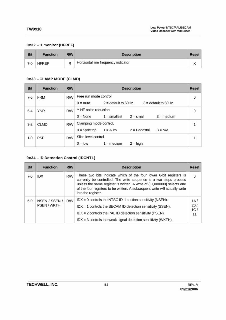
TW9910
TECHWELL, INC. 52 REV. A 09/21/2006
Low Power NTSC/PAL/SECAM Video Decoder with VBI Slicer
0x32 – H monitor (HFREF)
Bit Function R/W Description Reset
7-0 HFREF R Horizontal line frequency indicator X
0x33 – CLAMP MODE (CLMD)
Bit Function R/W Description Reset
7-6 FRM R/W Free run mode control
0 = Auto 2 = default to 60Hz 3 = default to 50Hz 0
5-4 YNR R/W Y HF noise reduction
0 = None 1 = smallest 2 = small 3 = medium 0
3-2 CLMD R/W Clamping mode control.
0 = Sync top 1 = Auto 2 = Pedestal 3 = N/A 1
1-0 PSP R/W Slice level control
0 = low 1 = medium 2 = high 1
0x34 – ID Detection Control (IDCNTL)
Bit Function R/W Description Reset
7-6 IDX R/W These two bits indicate which of the four lower 6-bit registers is currently be controlled. The write sequence is a two steps process unless the same register is written. A write of {ID,000000} selects one of the four registers to be written. A subsequent write will actually write into the register.
0
5-0 NSEN / SSEN / PSEN / WKTH
R/W IDX = 0 controls the NTSC ID detection sensitivity (NSEN).
IDX = 1 controls the SECAM ID detection sensitivity (SSEN).
IDX = 2 controls the PAL ID detection sensitivity (PSEN).
IDX = 3 controls the weak signal detection sensitivity (WKTH).
1A / 20 / 1C / 11
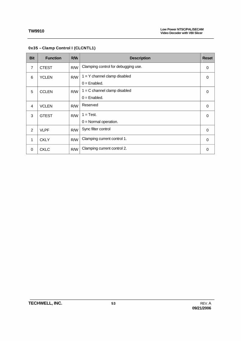
TW9910
TECHWELL, INC. 53 REV. A 09/21/2006
Low Power NTSC/PAL/SECAM Video Decoder with VBI Slicer
0x35 – Clamp Control I (CLCNTL1)
Bit Function R/W Description Reset
7 CTEST R/W Clamping control for debugging use. 0
6 YCLEN R/W 1 = Y channel clamp disabled
0 = Enabled. 0
5 CCLEN R/W 1 = C channel clamp disabled
0 = Enabled. 0
4 VCLEN R/W Reserved 0
3 GTEST R/W 1 = Test.
0 = Normal operation. 0
2 VLPF R/W Sync filter control 0
1 CKLY R/W Clamping current control 1. 0
0 CKLC R/W Clamping current control 2. 0

TW9910
TECHWELL, INC. 54 REV. A 09/21/2006
Low Power NTSC/PAL/SECAM Video Decoder with VBI Slicer
0x4F – WSS3
Bit Function R/W Description Reset
7-0 WSS[19:14] R CGMS(WSS525) Bit19-14 in 525 line video system. These bits show CRC 6bits in CGMS(WSS525). These bits are only valid in 525 line video system.
X
0x50 – FILLDATA
Bit Function R/W Description Reset
7-0 FILLDATA R/W Filled data as dummy data in ANC Dword data packet. A0
0x51 – SDID
Bit Function R/W Description Reset
7 NODAEN R/W 1:Bit7 in 4th byte of EAV/SAV code will be 0 when sync lost(No Video input.)
0: Bit7 in 4th byte of EAV/SAV is always VIPCFG register bit.
0
6 SYRM R/W 1: Minimum value in raw VBI will be 0x10 for Sync Level remove.
0:none. 0
5-0 SDID R/W Secondary data ID in ANC data packet type 2 22
0x52 – DID
Bit Function R/W Description Reset
7 ANCEN R/W ANC data packet output control. 1 = enable. 0:disable. 0
6 TOUTHA R/W 1: reserved
0:should be “0” in normal mode. 0
5 VIPCFG R/W Set up Bit7 in 4th byte of EAV/SAV code. 1
4-0 DID R/W Data ID in ANC data packet type 2. 11
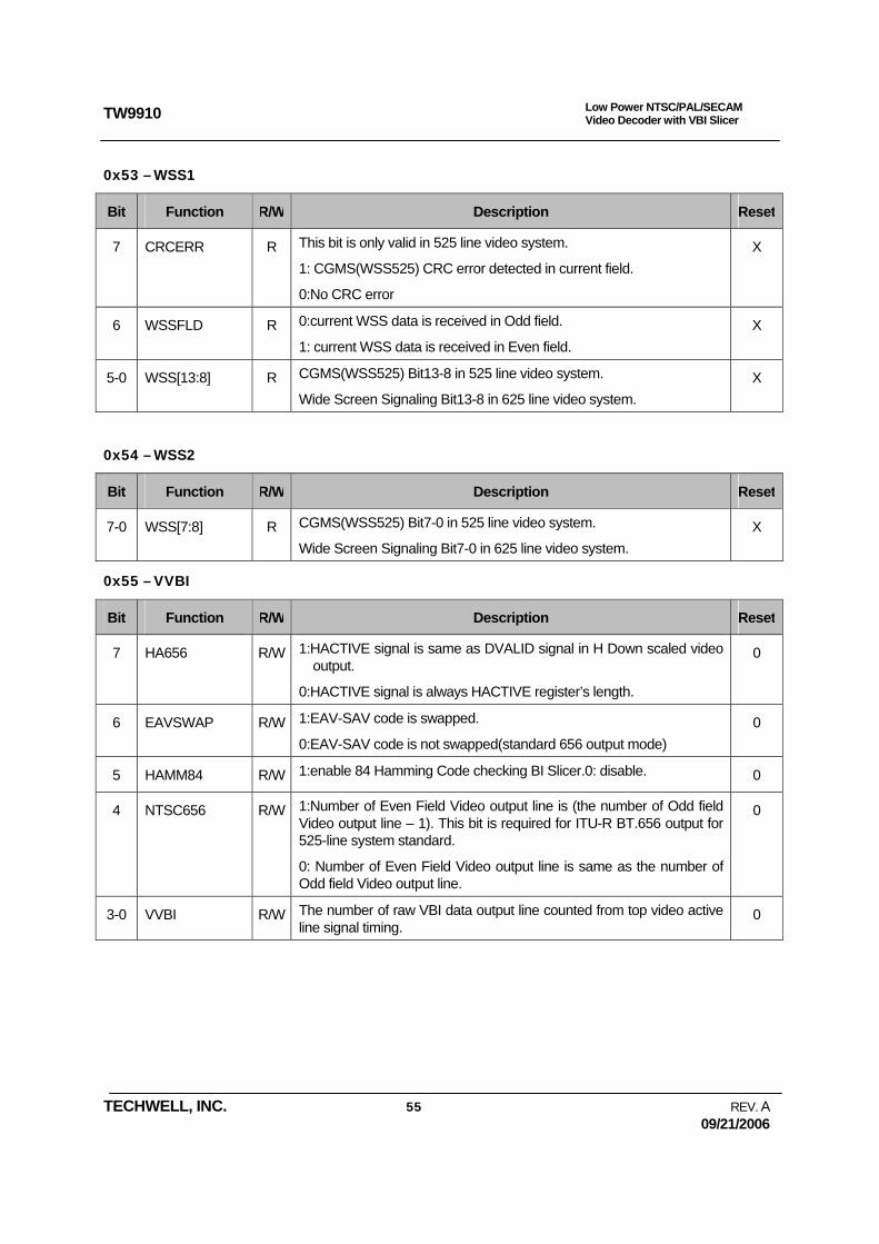
TW9910
TECHWELL, INC. 55 REV. A 09/21/2006
Low Power NTSC/PAL/SECAM Video Decoder with VBI Slicer
0x53 – WSS1
Bit Function R/W Description Reset
7 CRCERR R This bit is only valid in 525 line video system.
1: CGMS(WSS525) CRC error detected in current field.
0:No CRC error
X
6 WSSFLD R 0:current WSS data is received in Odd field.
1: current WSS data is received in Even field. X
5-0 WSS[13:8] R CGMS(WSS525) Bit13-8 in 525 line video system.
Wide Screen Signaling Bit13-8 in 625 line video system. X
0x54 – WSS2
Bit Function R/W Description Reset
7-0 WSS[7:8] R CGMS(WSS525) Bit7-0 in 525 line video system.
Wide Screen Signaling Bit7-0 in 625 line video system. X
0x55 – VVBI
Bit Function R/W Description Reset
7 HA656 R/W 1:HACTIVE signal is same as DVALID signal in H Down scaled video output.
0:HACTIVE signal is always HACTIVE register’s length.
0
6 EAVSWAP R/W 1:EAV-SAV code is swapped.
0:EAV-SAV code is not swapped(standard 656 output mode) 0
5 HAMM84 R/W 1:enable 84 Hamming Code checking BI Slicer.0: disable. 0
4 NTSC656 R/W 1:Number of Even Field Video output line is (the number of Odd field Video output line – 1). This bit is required for ITU-R BT.656 output for 525-line system standard.
0: Number of Even Field Video output line is same as the number of Odd field Video output line.
0
3-0 VVBI R/W The number of raw VBI data output line counted from top video active line signal timing.
0

TW9910
TECHWELL, INC. 56 REV. A 09/21/2006
Low Power NTSC/PAL/SECAM Video Decoder with VBI Slicer
0x56~6A LCTL6~LCTL26
Bit Function R/W Description Reset
7-4 R/W Set up VBI Data Slicer Decoding mode on Line-n.
Value is set up by upper bit7-4 meaning for Line-n in odd field. 0
3-0
LCTLn
R/W Value is set up by below bit3-0 meaning for Line-n in even field.
0h:disable decoding.
1h:Teletext-B
2h:Teletext-C
3h:Teletext-D
4h:Closed Captioning and Extended Data service. (EIA-608 type).
5h:CGMS (WSS525) in 525 line system or WSS625 in 625 line
system.
6h:VITC
7h:Gemstar 1x
8h:Gemstar 2x
9h:VPS (Line16 VPS type)
Ah: Teletext-A
Bh~Fh: reserved
0
0x6B – HSGEGIN
Bit Function R/W Description Reset
7-0 HSBEGIN R/W HSYNC Start position. 2C
0x6C – HSEND
Bit Function R/W Description Reset
7-0 HSEND R/W HSYNC End position. 60
0x6D – OVSDLY
Bit Function R/W Description Reset
7-0 OVSDLY R/W VSYNC Start position. 00

TW9910
TECHWELL, INC. 57 REV. A 09/21/2006
Low Power NTSC/PAL/SECAM Video Decoder with VBI Slicer
0x6E – OVSEND
Bit Function R/W Description Reset
7 HSPIN R/W 1:HSYNC output is HACTIVE.
0:HSYNC output is HSYNC. 0
6-4 OFDLY R/W FIELD output delay.
0h:0H line delay FIELD output. (601 mode only)
1h-6h: 1-H to 6-H line delay FIELD output.
7h:FIELD output is synchronized to the leading edge of VACTIVE.
2
3 VSMODE R/W 1:VSYNC output is HACTIVE-VSYNC mode.
0:VSYNC output is HSYNC-VSYNC mode. 0
2-0 OVSEND R/W Line delay for VSYNC end position. 0
0x6F – VBIDELAY
Bit Function R/W Description Reset
7 PDNSVBI R/W 1:VBI data slicer enable
0: VBI data slicer is in reset and power-down mode 0
6 Reserved R/W 0
5-0 VBIDELAY R/W Raw VBI output delay 24

TW9910
TECHWELL, INC. 58 REV. A 09/21/2006
Low Power NTSC/PAL/SECAM Video Decoder with VBI Slicer
Pin Diagram
44 PIN LQFP
VD[7] VD[8] VD[9] VD[10] VDD VD[11] VD[12] VD[13] VD[14] VD[15] VDDE
XTO
XT
I VS
SE
VD[0
]/SIA
D0
VD[1
] VS
S VD
[2]
VD[3
] VD
[4]
VD[5
] VD
[6]
TW9910
3332313029282726252423
1 2 3 4 5 6 7 8 9 10 11
12
13
14
15
16
17
18
19
20
21
22
44 43 42 41 40 39 38 37 36 35 34
VDDESCLKSDATPDN
RSTBTMODE
AVDYMUX3YMUX2YGND
YMUX1
YMU
X0AV
SC
IN0
AVD
AVS
VSS VS HS
MPO
UT
CLK
X2VS
SE

TW9910
TECHWELL, INC. 59 REV. A 09/21/2006
Low Power NTSC/PAL/SECAM Video Decoder with VBI Slicer
Pin Diagram
48 PIN QFN
VD[7] VD[8] VD[9] VD[10] VDD NC VD[11] VD[12] VD[13] VD[14] VD[15] VDDE
XTO
XT
I VS
SE
VD[0
]/SIA
D0
VD[1
] N
C
VS
S VD
[2]
VD[3
] VD
[4]
VD[5
] VD
[6]
TW9910
363534333231302928272625
1 2 3 4 5 6 7 8 9 10 11 12
13
14
15
16
17
18
19
20
21
22
23
24
48 47 46 45 44 43 42 41 40 39 38 37
VDDESCLKSDATPDN
RSTBTMODE
NCAVD
YMUX3YMUX2YGND
YMUX1
YMU
X0AV
SC
IN0
AVD
AVS
NC
VSS VS HS
MPO
UT
CLK
X2VS
SE

TW9910
TECHWELL, INC. 60 REV. A 09/21/2006
Low Power NTSC/PAL/SECAM Video Decoder with VBI Slicer
Pin Description
Pin#
LQFP QFN
I/O Pin Name
Description
Analog video signals
12 13 I MUX0 Analog CVBS or Y input. Connect unused input to AGND through 0.1uF capacitor.
11 12 I MUX1 Analog CVBS or Y input. Connect unused input to AGND through 0.1uF capacitor.
9 10 I MUX2 Analog CVBS or Y input. Connect unused input to AGND through 0.1uF capacitor.
8 9 I MUX3 Analog CVBS or Y input. Connect unused input to AGND through 0.1uF capacitor.
10 11 YGND Analog Differential input for Y-ADC.
14 15 I CIN0 Analog chroma input. Connect unused input to AGND through 0.1uF capacitor.
Clock Signals
43 47 I XTI Clock input. A 27Mhz fundamental (or 3rd overtone) crystal or a single-ended oscillator can be connected.
44 48 O XTO Clock output. For connecting a crystal.
Host Interface
2 2 I SCLK The MPU Serial interface Clock Line.
3 3 I/O SDAT The MPU Serial interface Data Line.
General signals
5 5 I RSTB Reset input. Low active.
4 4 I PDN Power down control pin. It is high active.
6 6 I TMODE Test pin. It should be low for normal operation.
7,18, 31,43
NC NC pin.
Video output Signals
19 21 O HS Horizontal sync and multi-purpose output pin. See register for control information.
18 20 O VS Vertical Sync and multi-purpose output. See register for control information.
21 23 O CLK2 Data Clock output. See register for control information.
20 22 O MPOUT Multi-purpose output pin. The output function can be selected by RTSEL of register 0x19
24,25,26,27,28,30,31,32
26,27,28,29,30,33,34,35
O VD[15:8] Digitized Video Data Outputs of Y/YCbCr. VD[8] is the LSB and VD[15] is the MSB.
33,34,35,36,37,38,
40
36,37, 38,39,40,41,
44
I/O VD[7:1] Digitized video data output of CbCr. VD[7] is the MSB.
41 45 I/O VD[0]/
SIAD0
LSB of digitized video data output of CbCr.
SIAD0 : The MPU interface address select pin 0. A pullup or pulldown resister is needed for select one of the two addresses that chip will respond.
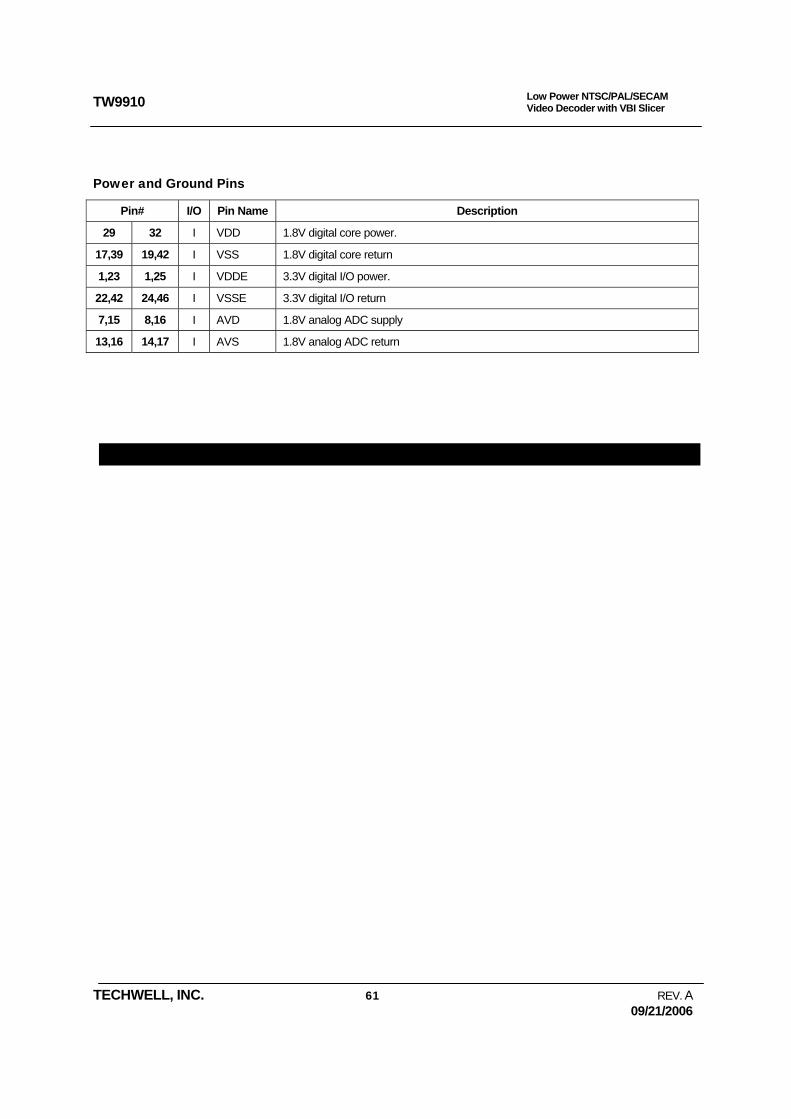
TW9910
TECHWELL, INC. 61 REV. A 09/21/2006
Low Power NTSC/PAL/SECAM Video Decoder with VBI Slicer
Power and Ground Pins
Pin# I/O Pin Name Description
29 32 I VDD 1.8V digital core power.
17,39 19,42 I VSS 1.8V digital core return
1,23 1,25 I VDDE 3.3V digital I/O power.
22,42 24,46 I VSSE 3.3V digital I/O return
7,15 8,16 I AVD 1.8V analog ADC supply
13,16 14,17 I AVS 1.8V analog ADC return
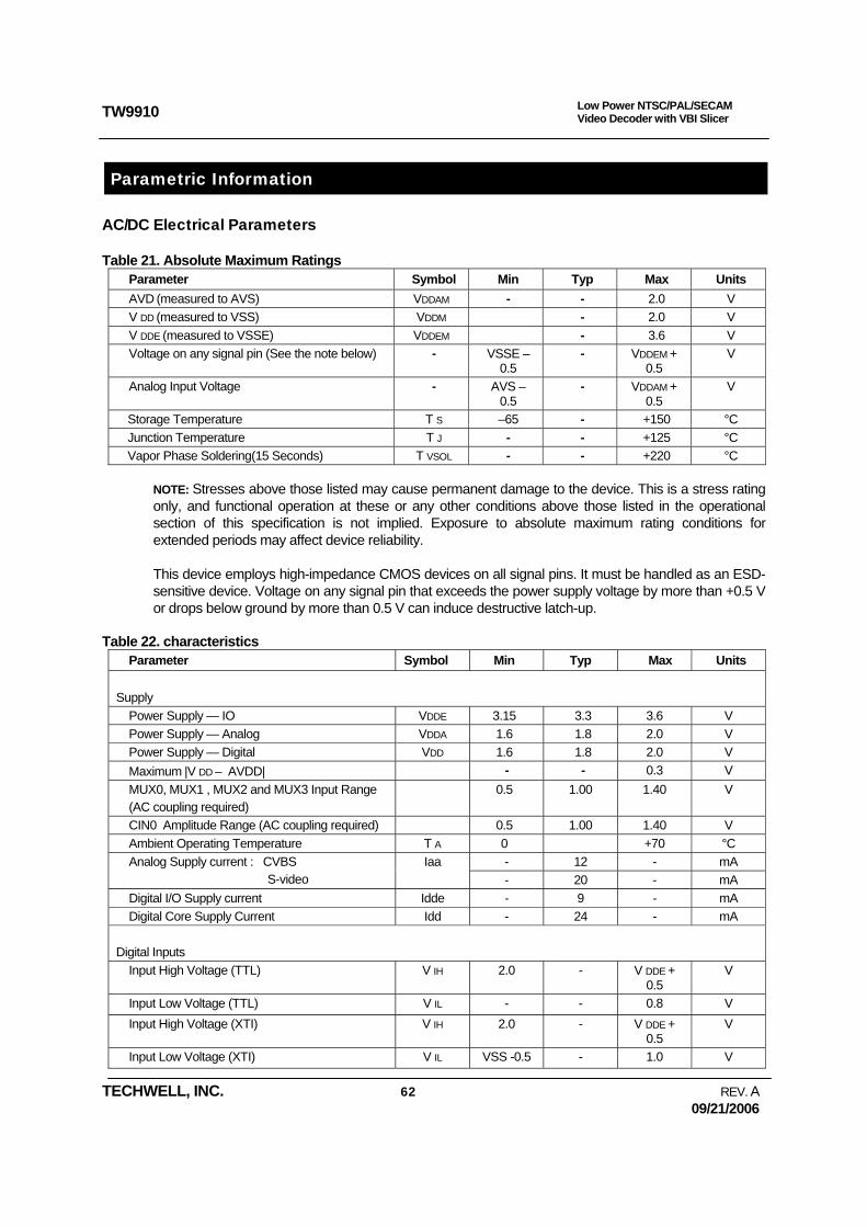
TW9910
TECHWELL, INC. 62 REV. A 09/21/2006
Low Power NTSC/PAL/SECAM Video Decoder with VBI Slicer
Parametric Information
AC/DC Electrical Parameters
Table 21. Absolute Maximum Ratings Parameter Symbol Min Typ Max Units AVD (measured to AVS) VDDAM - - 2.0 V V DD (measured to VSS) VDDM - 2.0 V V DDE (measured to VSSE) VDDEM - 3.6 V Voltage on any signal pin (See the note below) - VSSE –
0.5 - VDDEM +
0.5 V
Analog Input Voltage - AVS – 0.5
- VDDAM + 0.5
V
Storage Temperature T S –65 - +150 °C Junction Temperature T J - - +125 °C Vapor Phase Soldering(15 Seconds) T VSOL - - +220 °C
NOTE: Stresses above those listed may cause permanent damage to the device. This is a stress rating only, and functional operation at these or any other conditions above those listed in the operational section of this specification is not implied. Exposure to absolute maximum rating conditions for extended periods may affect device reliability.
This device employs high-impedance CMOS devices on all signal pins. It must be handled as an ESD-sensitive device. Voltage on any signal pin that exceeds the power supply voltage by more than +0.5 V or drops below ground by more than 0.5 V can induce destructive latch-up.
Table 22. characteristics Parameter Symbol Min Typ Max Units
Supply
Power Supply — IO VDDE 3.15 3.3 3.6 V Power Supply — Analog VDDA 1.6 1.8 2.0 V Power Supply — Digital VDD 1.6 1.8 2.0 V Maximum |V DD – AVDD| - - 0.3 V MUX0, MUX1 , MUX2 and MUX3 Input Range (AC coupling required)
0.5 1.00 1.40 V
CIN0 Amplitude Range (AC coupling required) 0.5 1.00 1.40 V Ambient Operating Temperature T A 0 +70 °C
- 12 - mA Analog Supply current : CVBS S-video
Iaa - 20 - mA
Digital I/O Supply current Idde - 9 - mA Digital Core Supply Current Idd - 24 - mA
Digital Inputs
Input High Voltage (TTL) V IH 2.0 - V DDE + 0.5
V
Input Low Voltage (TTL) V IL - - 0.8 V Input High Voltage (XTI) V IH 2.0 - V DDE +
0.5 V
Input Low Voltage (XTI) V IL VSS -0.5 - 1.0 V

TW9910
TECHWELL, INC. 63 REV. A 09/21/2006
Low Power NTSC/PAL/SECAM Video Decoder with VBI Slicer
Input High Current (V IN =V DD ) I IH - - 10 µA Input Low Current (V IN =VSS) I IL - - –10 µA Input Capacitance (f=1 MHz, V IN =2.4 V) C IN - 5 - pF
Parameter Symbol Min Typ Max Units Digital Outputs
Output High Voltage (I OH = –2 mA) V OH 2.4 - V DDE V
Output Low Voltage (I OL = 2 mA) V OL - 0.2 0.4 V
3-State Current I OZ - - 10 µA
Output Capacitance C O - 5 - pF
Analog Input
Analog Pin Input voltage Vi - 1 - Vpp Analog Pin Input Capacitance C A - 7 - pF
ADCs
ADC resolution ADCR - 10 - bits ADC integral Non-linearity AINL - ±1 - LSB ADC differential non-linearity ADNL - ±1 - LSB ADC clock rate fADC 24 27 30 MHz Video bandwidth (-3db) BW - 10 - MHz
Horizontal PLL
Line frequency (50Hz) fLN - 15.625 - KHz Line frequency (60Hz) fLN - 15.734 - KHz static deviation ∆fH - - 6.2 %
Subcarrier PLL
subcarrier frequency (NTSC-M) fSC - 3579545 - Hz subcarrier frequency (PAL-BDGHI) fSC - 4433619 - Hz subcarrier frequency (PAL-M) fSC - 3575612 - Hz subcarrier frequency (PAL-N) fSC - 3582056 - Hz lock in range ∆fH ±450 - - Hz
Crystal spec
nominal frequency (fundamental) - 27 - MHz deviation - - ±50 ppm Temperature range Ta 0 - 70 oC load capacitance CL - 20 - pF series resistor RS - 80 - Ohm
Oscillator Input
nominal frequency - 27 - MHz deviation - - ±50 ppm duty cycle - - 55 %

TW9910
TECHWELL, INC. 64 REV. A 09/21/2006
Low Power NTSC/PAL/SECAM Video Decoder with VBI Slicer
Parameter Symbol Min Typ Max Units Output CLK
CLKX1 12 13.5 15 MHz CLKX2 24 27 30 MHz CLKX1 Duty Cycle - - 55 % CLKX2 Duty Cycle - - 55 % CLKX2 to CLKX1 Delay 4 - - 2 ns CLKX1 to Data Delay 5 - 5 - ns CLKX2 to Data Delay 6 - 5 - ns CLKX1 (Falling Edge) to VCLK (Rising Edge) 41 - 0 - ns CLKX2 (Falling Edge) to VCLK (Rising Edge) 42 - 0 - ns
Output Video Data 8-bit Mode (1)
Data to VCLK (Rising Edge) Delay 7b - 18 - ns VCLK (Rising Edge) to Data Delay 8b - 18 - ns
16-bit Mode (1) Data to VCLK (Rising Edge) Delay 7a - 37 - ns VCLK (Rising Edge) to Data Delay 8a - 37 - ns
Clock Timing Diagram
XT
CLKX2
CLKX1
VCLK
Data
1 2
7b 8b6
4
7a 8a
5
41
42
3
VCLK
Data
(8-bit output mode)
(16-bit output mode)

TW9910
TECHWELL, INC. 65 REV. A 09/21/2006
Low Power NTSC/PAL/SECAM Video Decoder with VBI Slicer
Mechanical Data
44 Pin LQFP
A1
A
A2
L1
c
E
E1E2
be
TW9910
Top View
D D1 D2
R2
R1
S L θ3
θ2
Gage Plane 0.25mm
θ
θ1
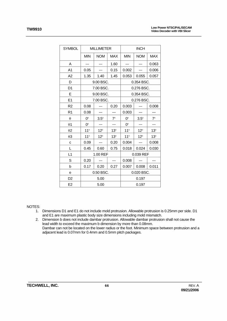
TW9910
TECHWELL, INC. 66 REV. A 09/21/2006
Low Power NTSC/PAL/SECAM Video Decoder with VBI Slicer
NOTES:
1. Dimensions D1 and E1 do not include mold protrusion. Allowable protrusion is 0.25mm per side. D1 and E1 are maximum plastic body size dimensions including mold mismatch.
2. Dimension b does not include dambar protrusion. Allowable dambar protrusion shall not cause the lead width to exceed the maximum b dimension by more than 0.08mm. Dambar can not be located on the lower radius or the foot. Minimum space between protrusion and a adjacent lead is 0.07mm for 0.4mm and 0.5mm pitch packages.
MILLIMETER INCH SYMBOL
MIN NOM MAX MIN NOM MAX
A --- --- 1.60 --- --- 0.063 A1 0.05 --- 0.15 0.002 --- 0.006 A2 1.35 1.40 1.45 0.053 0.055 0.057 D 9.00 BSC. 0.354 BSC. D1 7.00 BSC. 0.276 BSC. E 9.00 BSC. 0.354 BSC. E1 7.00 BSC. 0.276 BSC. R2 0.08 --- 0.20 0.003 --- 0.008 R1 0.08 --- --- 0.003 --- ---
θ 0° 3.5° 7° 0° 3.5° 7° θ1 0° --- --- 0° --- ---
θ2 11° 12° 13° 11° 12° 13° θ3 11° 12° 13° 11° 12° 13° c 0.09 --- 0.20 0.004 --- 0.008 L 0.45 0.60 0.75 0.018 0.024 0.030 L1 1.00 REF 0.039 REF S 0.20 --- --- 0.008 --- --- b 0.17 0.20 0.27 0.007 0.008 0.011 e 0.50 BSC. 0.020 BSC.
D2 5.00 0.197 E2 5.00 0.197

TW9910
TECHWELL, INC. 67 REV. A 09/21/2006
Low Power NTSC/PAL/SECAM Video Decoder with VBI Slicer
48 PIN QFN

TW9910
TECHWELL, INC. 68 REV. A 09/21/2006
Low Power NTSC/PAL/SECAM Video Decoder with VBI Slicer
NOTES:
1. All dimensions are in millimeters. 2. Dimension applies to plated terminal and is measured between 0.20 and 0.25mm from terminal tip. 3. Package warpage MAX 0.08mm. 4. Package corners unless otherwise specified are R0.175± 0.025mm
MILLIMETER INCH SYMBOL
MIN NOM MAX MIN NOM MAX
A --- --- 0.90 --- --- 0.035 A1 0.00 0.01 0.05 0.00 0.0004 0.002 A2 --- 0.65 0.70 --- 0.026 0.028 A3 0.2 REF. 0.008 REF. b 0.20 0.25 0.32 0.008 0.010 0.013 D 7.00 BSC. 0.276 BSC. D1 6.75 BSC. 0.266 BSC. D2 5.00 5.20 5.40 0.197 0.205 0.213 E 7.00 BSC. 0.276 BSC. E1 6.75 BSC. 0.266 BSC. E2 5.00 5.20 5.40 0.197 0.205 0.213 L 0.30 0.40 0.50 0.012 0.016 0.020 e 0.50 BSC. 0.020 BSC.
θ1 0° --- 12° 0° --- 12° R 0.09 --- --- 0.004 --- ---
TOLERANCES OF FORM AND POSITION aaa 0.10 0.004 bbb 0.10 0.004 ccc 0.05 0.002
* CONTROLLING DIMENSION : MM

TW9910
TECHWELL, INC. 69 REV. A 09/21/2006
Low Power NTSC/PAL/SECAM Video Decoder with VBI Slicer
Application Schematics
MUX0
MUX1
CIN0
22pf27M1Mohm
22pf
L1, 3.3uHC1, 220pf
XTI
XTO
RST#
VD1-15
VideoTiming
SCL
SDA
TMODEPDN
AGND
DGND
0.1uF
AVDD
AGND
0.1uF
DVDD
DGNDGND
1.8V3.3V
Filtered 1.8V
Typical TW9910 External Circuitry
4.7k
4.7k
3.3/5V
TW9910
CVBS1
S-Video
Note: All unused digital input pins should be tied to DGND.
*
* For 3rd overtone crystal
0.1uF75 ohm
0.1uF75 ohm
0.1uF75 ohm
VD0 / SIAD0
3.3V
** option10k
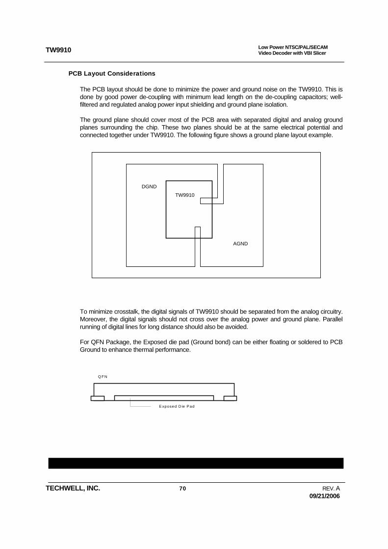
TW9910
TECHWELL, INC. 70 REV. A 09/21/2006
Low Power NTSC/PAL/SECAM Video Decoder with VBI Slicer
PCB Layout Considerations
The PCB layout should be done to minimize the power and ground noise on the TW9910. This is done by good power de-coupling with minimum lead length on the de-coupling capacitors; well-filtered and regulated analog power input shielding and ground plane isolation.
The ground plane should cover most of the PCB area with separated digital and analog ground planes surrounding the chip. These two planes should be at the same electrical potential and connected together under TW9910. The following figure shows a ground plane layout example.
AGND
DGND
TW9910
To minimize crosstalk, the digital signals of TW9910 should be separated from the analog circuitry. Moreover, the digital signals should not cross over the analog power and ground plane. Parallel running of digital lines for long distance should also be avoided.
For QFN Package, the Exposed die pad (Ground bond) can be either floating or soldered to PCB Ground to enhance thermal performance.
E xposed D ie P ad
Q FN
TW9910
TECHWELL, INC. 71 REV. A 09/21/2006
Low Power NTSC/PAL/SECAM Video Decoder with VBI Slicer
Copyright Notice
This manual is copyrighted by Techwell, Inc. Do not reproduce, transform to any other format, or send/transmit any part of this documentation without the express written permission of Techwell, Inc.
Disclaimer
This document provides technical information for the user. Techwell, Inc. reserves the right to modify the information in this document as necessary. The customer should make sure that they have the most recent data sheet version. Techwell, Inc. holds no responsibility for any errors that may appear in this document. Customers should take appropriate action to ensure their use of the products does not infringe upon any patents. Techwell, Inc. respects valid patent rights of third parties and does not infringe upon or assist others to infringe upon such rights.
Life Support Policy
Techwell, Inc. products are not authorized for use as critical components in life support devices or systems.
Datasheet revision history
Date
12/14/2005 First draft.
12/27/2005 Add MPOUT pin description. Change Oscillator Input deviation +/25 to +/- 50
01/24/2006 Add LQFP.
02/20/2006 Pg61, Fix pin number, LQFP pin17 to pin16. Pg27 Reg. Table 0x1E. Pg28 Reg. Table 0x4F.
03/08/2006 Pg62, change symbols. AVD, AVS. Pg27. Reg 0x16, reset:00.
09/21/2006 P70, add exposed die pad info.