RGB to NTSC/PAL Encoder AD722 -...
12
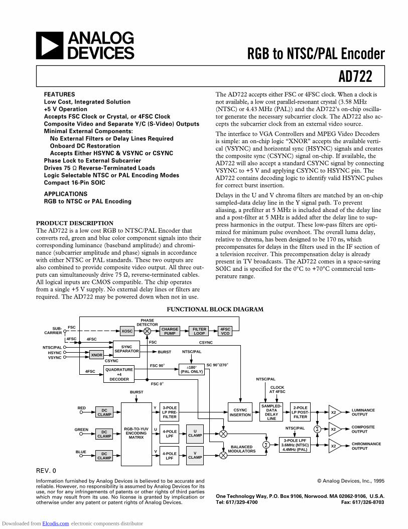
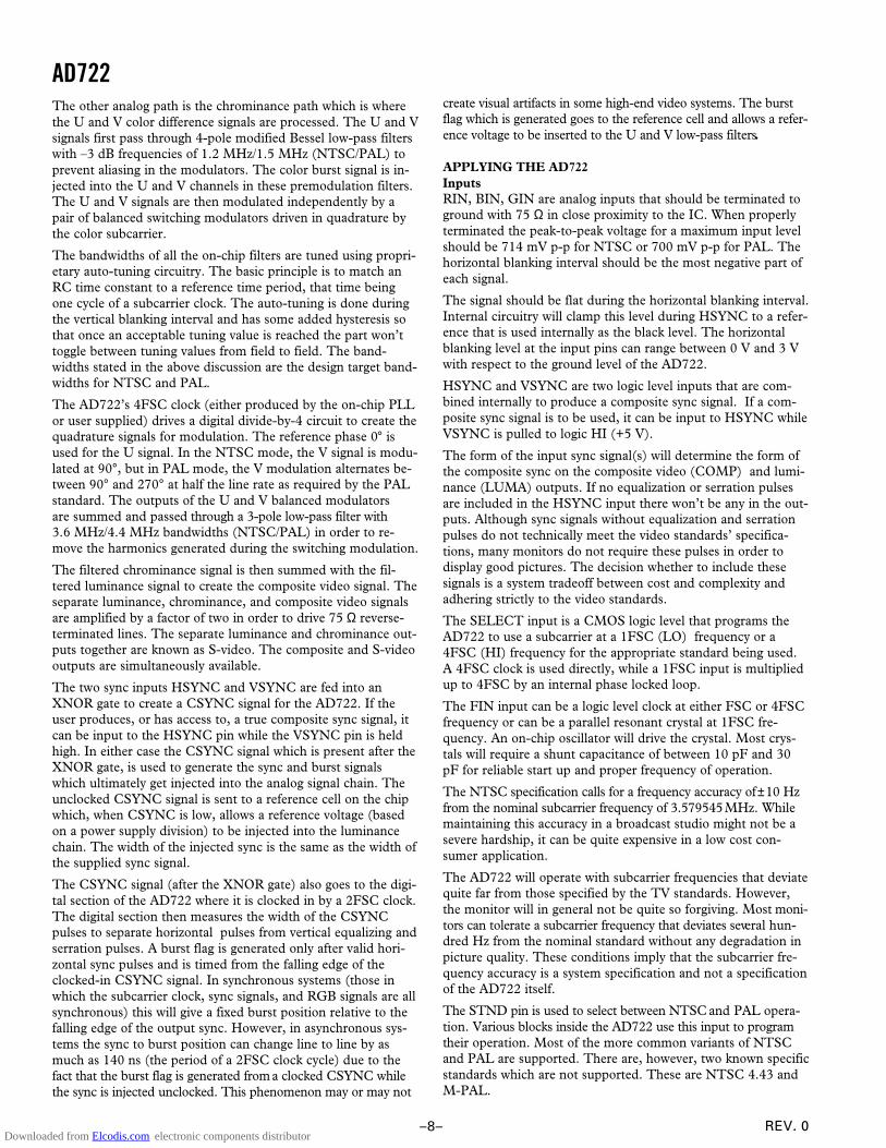
a RGB to NTSC/PAL Encoder AD722 © Analog Devices, Inc., 1995 One Technology Way, P.O. Box 9106, Norwood. MA 02062-9106, U.S.A. Tel: 617/329-4700 Fax: 617/326-8703 FEATURES Low Cost, Integrated Solution +5 V Operation Accepts FSC Clock or Crystal, or 4FSC Clock Composite Video and Separate Y/C (S-Video) Outputs Minimal External Components: No External Filters or Delay Lines Required Onboard DC Restoration Accepts Either HSYNC & VSYNC or CSYNC Phase Lock to External Subcarrier Drives 75 Ω Reverse-Terminated Loads Logic Selectable NTSC or PAL Encoding Modes Compact 16-Pin SOIC APPLICATIONS RGB to NTSC or PAL Encoding PRODUCT DESCRIPTION The AD722 is a low cost RGB to NTSC/PAL Encoder that converts red, green and blue color component signals into their corresponding luminance (baseband amplitude) and chromi- nance (subcarrier amplitude and phase) signals in accordance with either NTSC or PAL standards. These two outputs are also combined to provide composite video output. All three out- puts can simultaneously drive 75 Ω, reverse-terminated cables. All logical inputs are CMOS compatible. The chip operates from a single +5 V supply. No external delay lines or filters are required. The AD722 may be powered down when not in use. The AD722 accepts either FSC or 4FSC clock. When a clock is not available, a low cost parallel-resonant crystal (3.58 MHz (NTSC) or 4.43 MHz (PAL)) and the AD722’s on-chip oscilla- tor generate the necessary subcarrier clock. The AD722 also ac- cepts the subcarrier clock from an external video source. The interface to VGA Controllers and MPEG Video Decoders is simple: an on-chip logic “XNOR” accepts the available verti- cal (VSYNC) and horizontal sync (HSYNC) signals and creates the composite sync (CSYNC) signal on-chip. If available, the AD722 will also accept a standard CSYNC signal by connecting VSYNC to +5 V and applying CSYNC to HSYNC pin. The AD722 contains decoding logic to identify valid HSYNC pulses for correct burst insertion. Delays in the U and V chroma filters are matched by an on-chip sampled-data delay line in the Y signal path. To prevent aliasing, a prefilter at 5 MHz is included ahead of the delay line and a post-filter at 5 MHz is added after the delay line to sup- press harmonics in the output. These low-pass filters are opti- mized for minimum pulse overshoot. The overall luma delay, relative to chroma, has been designed to be 170 ns, which precompensates for delays in the filters used in the IF section of a television receiver. This precompensation delay is already present in TV broadcasts. The AD722 comes in a space-saving SOIC and is specified for the 0°C to +70°C commercial tem- perature range. FUNCTIONAL BLOCK DIAGRAM PHASE DETECTOR SYNC SEPARATOR XOSC CHARGE PUMP FILTER LOOP 4FSC VCO XNOR 4FSC 4FSC FSC SUB- CARRIER NTSC/PAL HSYNC VSYNC BURST QUADRATURE +4 DECODER ±180° (PAL ONLY) NTSC/PAL FSC 90° FSC 0° 4FSC SC 90°/270° FSC CSYNC CSYNC DC CLAMP RED GREEN BLUE RGB-TO-YUV ENCODING MATRIX BURST Y 3-POLE LP PRE- FILTER U V 4-POLE LPF 4-POLE LPF BALANCED MODULATORS 3-POLE LPF 3.6MHz (NTSC) 4.4MHz (PAL) NTSC/PAL CSYNC INSERTION SAMPLED- DATA DELAY LINE 2-POLE LP POST- FILTER X2 X2 X2 LUMINANCE OUTPUT COMPOSITE OUTPUT CHROMINANCE OUTPUT U CLAMP V CLAMP NTSC/PAL CLOCK AT 4FSC DC CLAMP DC CLAMP REV. 0 Information furnished by Analog Devices is believed to be accurate and reliable. However, no responsibility is assumed by Analog Devices for its use, nor for any infringements of patents or other rights of third parties which may result from its use. No license is granted by implication or otherwise under any patent or patent rights of Analog Devices. Downloaded from Elcodis.com electronic components distributor
Transcript of RGB to NTSC/PAL Encoder AD722 -...
a RGB to NTSC/PAL EncoderAD722
© Analog Devices, Inc., 1995
One Technology Way, P.O. Box 9106, Norwood. MA 02062-9106, U.S.A.
Tel: 617/329-4700 Fax: 617/326-8703
FEATURES
Low Cost, Integrated Solution
+5 V Operation
Accepts FSC Clock or Crystal, or 4FSC Clock
Composite Video and Separate Y/C (S-Video) Outputs
Minimal External Components:
No External Filters or Delay Lines Required
Onboard DC Restoration
Accepts Either HSYNC & VSYNC or CSYNC
Phase Lock to External Subcarrier
Drives 75 Ω Reverse-Terminated Loads
Logic Selectable NTSC or PAL Encoding Modes
Compact 16-Pin SOIC
APPLICATIONS
RGB to NTSC or PAL Encoding
PRODUCT DESCRIPTIONThe AD722 is a low cost RGB to NTSC/PAL Encoder thatconverts red, green and blue color component signals into theircorresponding luminance (baseband amplitude) and chromi-nance (subcarrier amplitude and phase) signals in accordancewith either NTSC or PAL standards. These two outputs arealso combined to provide composite video output. All three out-puts can simultaneously drive 75 Ω, reverse-terminated cables.All logical inputs are CMOS compatible. The chip operatesfrom a single +5 V supply. No external delay lines or filters arerequired. The AD722 may be powered down when not in use.
The AD722 accepts either FSC or 4FSC clock. When a clock isnot available, a low cost parallel-resonant crystal (3.58 MHz(NTSC) or 4.43 MHz (PAL)) and the AD722’s on-chip oscilla-tor generate the necessary subcarrier clock. The AD722 also ac-cepts the subcarrier clock from an external video source.
The interface to VGA Controllers and MPEG Video Decodersis simple: an on-chip logic “XNOR” accepts the available verti-cal (VSYNC) and horizontal sync (HSYNC) signals and createsthe composite sync (CSYNC) signal on-chip. If available, theAD722 will also accept a standard CSYNC signal by connectingVSYNC to +5 V and applying CSYNC to HSYNC pin. TheAD722 contains decoding logic to identify valid HSYNC pulsesfor correct burst insertion.
Delays in the U and V chroma filters are matched by an on-chipsampled-data delay line in the Y signal path. To preventaliasing, a prefilter at 5 MHz is included ahead of the delay lineand a post-filter at 5 MHz is added after the delay line to sup-press harmonics in the output. These low-pass filters are opti-mized for minimum pulse overshoot. The overall luma delay,relative to chroma, has been designed to be 170 ns, whichprecompensates for delays in the filters used in the IF section ofa television receiver. This precompensation delay is alreadypresent in TV broadcasts. The AD722 comes in a space-savingSOIC and is specified for the 0°C to +70°C commercial tem-perature range.
FUNCTIONAL BLOCK DIAGRAM
PHASEDETECTOR
CHARGEPUMP
FILTERLOOPXOSC 4FSC
VCO
SYNCSEPARATOR
XNOR
XOSC CHARGEPUMP
FILTERLOOP
4FSCVCO
XNOR
4FSC 4FSC
FSCSUB-CARRIER
NTSC/PALHSYNCVSYNC
BURST
QUADRATURE+4
DECODER
±180°(PAL ONLY)
NTSC/PAL
FSC 90°
FSC 0°
4FSC
SC 90°/270°
FSC CSYNC
CSYNC
DCCLAMP
RED
GREEN
BLUE
RGB-TO-YUVENCODING
MATRIX
BURST
Y 3-POLELP PRE-FILTER
U
V
4-POLELPF
4-POLELPF
BALANCEDMODULATORS
3-POLE LPF3.6MHz (NTSC)4.4MHz (PAL)
NTSC/PAL
CSYNCINSERTION
SAMPLED-DATA
DELAYLINE
2-POLELP POST-FILTER
X2
X2
X2
LUMINANCEOUTPUT
COMPOSITEOUTPUT
CHROMINANCEOUTPUT
UCLAMP
VCLAMP
NTSC/PAL
CLOCKAT 4FSC
DCCLAMP
DCCLAMP
REV. 0
Information furnished by Analog Devices is believed to be accurate andreliable. However, no responsibility is assumed by Analog Devices for itsuse, nor for any infringements of patents or other rights of third partieswhich may result from its use. No license is granted by implication orotherwise under any patent or patent rights of Analog Devices.
Downloaded from Elcodis.com electronic components distributor
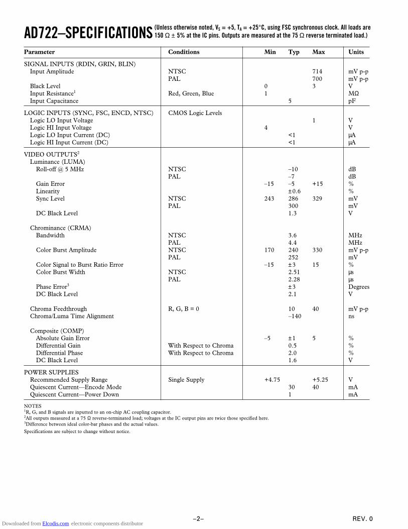
AD722–SPECIFICATIONS
REV. 0–2–
(Unless otherwise noted, VS = +5, TA = +25°C, using FSC synchronous clock. All loads are150 Ω ± 5% at the IC pins. Outputs are measured at the 75 Ω reverse terminated load.)
Parameter Conditions Min Typ Max Units
SIGNAL INPUTS (RDIN, GRIN, BLIN)Input Amplitude NTSC 714 mV p-p
PAL 700 mV p-pBlack Level 0 3 VInput Resistance1 Red, Green, Blue 1 MΩInput Capacitance 5 pF
LOGIC INPUTS (SYNC, FSC, ENCD, NTSC) CMOS Logic LevelsLogic LO Input Voltage 1 VLogic HI Input Voltage 4 VLogic LO Input Current (DC) <1 µALogic HI Input Current (DC) <1 µA
VIDEO OUTPUTS2
Luminance (LUMA)Roll-off @ 5 MHz NTSC –10 dB
PAL –7 dBGain Error –15 –5 +15 %Linearity ±0.6 %Sync Level NTSC 243 286 329 mV
PAL 300 mVDC Black Level 1.3 V
Chrominance (CRMA)Bandwidth NTSC 3.6 MHz
PAL 4.4 MHzColor Burst Amplitude NTSC 170 240 330 mV p-p
PAL 252 mVColor Signal to Burst Ratio Error –15 ±3 15 %Color Burst Width NTSC 2.51 µs
PAL 2.28 µsPhase Error3 ±3 DegreesDC Black Level 2.1 V
Chroma Feedthrough R, G, B = 0 10 40 mV p-pChroma/Luma Time Alignment –140 ns
Composite (COMP)Absolute Gain Error –5 ±1 5 %Differential Gain With Respect to Chroma 0.5 %Differential Phase With Respect to Chroma 2.0 %DC Black Level 1.6 V
POWER SUPPLIESRecommended Supply Range Single Supply +4.75 +5.25 VQuiescent Current—Encode Mode 30 40 mAQuiescent Current—Power Down 1 mA
NOTES1R, G, and B signals are inputted to an on-chip AC coupling capacitor.2All outputs measured at a 75 Ω reverse-terminated load; voltages at the IC output pins are twice those specified here.3Difference between ideal color-bar phases and the actual values.
Specifications are subject to change without notice.
Downloaded from Elcodis.com electronic components distributor
AD722
REV. 0 –3–
ORDERING GUIDE
Temperature Package PackageModel Range Description Option
AD722JR-16 0°C to +70°C 16-Pin SOIC R-16AD722JR-16-Reel 0°C to +70°C 16-Pin SOIC R-16AD722JR-16-Reel7 0°C to +70°C 16-Pin SOIC R-16
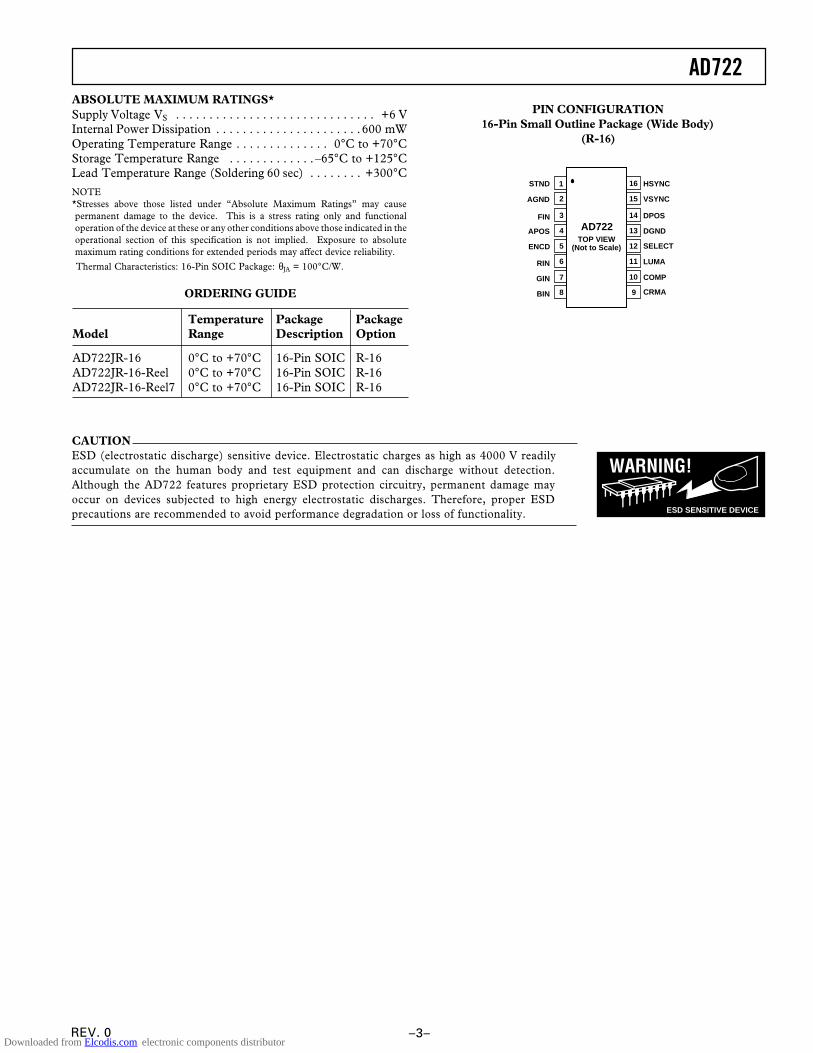
ABSOLUTE MAXIMUM RATINGS*Supply Voltage VS . . . . . . . . . . . . . . . . . . . . . . . . . . . . . . +6 VInternal Power Dissipation . . . . . . . . . . . . . . . . . . . . . .600 mWOperating Temperature Range . . . . . . . . . . . . . . 0°C to +70°CStorage Temperature Range . . . . . . . . . . . . . –65°C to +125°CLead Temperature Range (Soldering 60 sec) . . . . . . . . +300°CNOTE*Stresses above those listed under “Absolute Maximum Ratings” may causepermanent damage to the device. This is a stress rating only and functionaloperation of the device at these or any other conditions above those indicated in theoperational section of this specification is not implied. Exposure to absolutemaximum rating conditions for extended periods may affect device reliability.
Thermal Characteristics: 16-Pin SOIC Package: θJA = 100°C/W.
PIN CONFIGURATION16-Pin Small Outline Package (Wide Body)
(R-16)
AGND
ENCD
RIN
GIN
FIN
APOS
BIN
STND HSYNC
VSYNC
SELECT
LUMA
COMP
DPOS
DGND
CRMA
1
2
16
15
5
6
7
12
11
10
3
4
14
13
8 9
TOP VIEW(Not to Scale)
AD722
WARNING!
ESD SENSITIVE DEVICE
CAUTIONESD (electrostatic discharge) sensitive device. Electrostatic charges as high as 4000 V readilyaccumulate on the human body and test equipment and can discharge without detection.Although the AD722 features proprietary ESD protection circuitry, permanent damage mayoccur on devices subjected to high energy electrostatic discharges. Therefore, proper ESDprecautions are recommended to avoid performance degradation or loss of functionality.
Downloaded from Elcodis.com electronic components distributor
REV. 0–4–
AD722PIN DESCRIPTIONS
Pin Mnemonic Description Equivalent Circuit
1 STND A Logical HIGH input selects NTSC encoding. Circuit AA Logical LOW input selects PAL encoding.CMOS Logic Levels.
2 AGND Analog Ground Connection.3 FIN FSC clock or parallel-resonant crystal, or 4FSC clock input. Circuit B
For NTSC: 3.579 545 MHz or 14.318 180 MHz.For PAL: 4.433 619 MHz or 17.734 480 MHz.CMOS Logic Levels for subcarrier clocks.
4 APOS Analog Positive Supply (+5 V ± 5%).5 ENCD A Logical HIGH input enables the encode function. Circuit A
A Logical LOW input powers down chip when not in use.CMOS Logic Levels.
6 RIN Red Component Video Input. Circuit C0 to 714 mV for NTSC; 0 to 700 mV for PAL.
7 GIN Green Component Video Input. Circuit C0 to 714 mV for NTSC.0 to 700 mV for PAL.
8 BIN Blue Component Video Input. Circuit C0 to 714 mV for NTSC.0 to 700 mV for PAL.
9 CRMA Chrominance Output (Subcarrier Only).* Circuit DApproximately 1.8 V peak-to-peak for both NTSC and PAL.
10 COMP Composite Video Output.* Circuit DApproximately 2.5 V peak-to-peak for both NTSC and PAL.
11 LUMA Luminance plus SYNC Output.* Circuit DApproximately 2 V peak-to-peak for both NTSC and PAL.
12 SELECT A Logical LOW input selects the FSC operating mode. Circuit AA Logical HIGH input selects the 4FSC operating mode.CMOS Logic Levels.
13 DGND Digital Ground Connections.14 DPOS Digital Positive Supply (+5 V ± 5%) .15 VSYNC Vertical Sync Signal (if using external CSYNC set at +5 V). Circuit A16 HSYNC Horizontal Sync Signal (or CSYNC signal). Circuit A
*The Luminance, Chrominance, and Composite Outputs are at twice normal levels for driving 75 Ω reverse-terminated lines.
Equivalent Circuits
5
1
12
15
16
DPOS
3
VBIAS
APOS
10
9
11
APOS
7
VCLAMP
6
8
APOS
4pFTYP
Circuit B Circuit D
Circuit CCircuit A
Downloaded from Elcodis.com electronic components distributor
REV. 0 –5–
IRE
µs
0.10
0.5
–0.50 6010 20 30 40 50
0.0
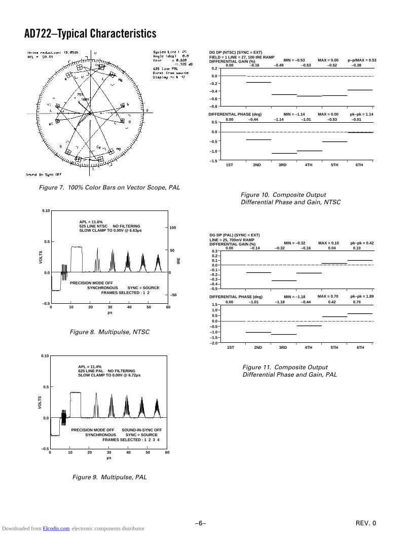
APL = 50.8%525 LINE NTSC NO FILTERINGSLOW CLAMP TO 0.00V @ 6.63µs
PRECISION MODE OFF SYNCHRONOUS SYNC = SOURCE FRAMES SELECTED : 1 2
100
50
0
–50
VO
LT
S
Figure 4. 100% Color Bars, NTSC
µs
0.10
0.5
–0.50 6010 20 30 40 50
0.0
VO
LT
S
APL = 50.6%625 LINE PAL NO FILTERINGSLOW CLAMP TO 0.00V @ 6.72µs
PRECISION MODE OFF SOUND-IN-SYNC OFF SYNCHRONOUS SYNC = SOURCE FRAMES SELECTED : 1 2 3 4
Figure 5. 100% Color Bars, PAL
Figure 6. 100% Color Bars on Vector Scope, NTSC
RGB
3
75Ω
75Ω
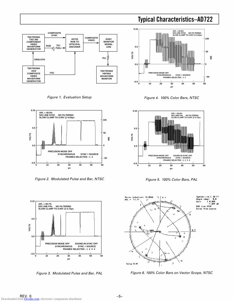
TEKTRONIXTSG 300
COMPONENTVIDEO
WAVEFORMGENERATOR
AD722RGB TO
NTSC/PALENCODER
SONYMONITORMODEL
1342
COMPOSITEVIDEO
COMPOSITESYNC
TEKTRONIXVM700A
WAVEFORMMONITOR
TEKTRONIX1910
COMPOSITEVIDEO
WAVEFORMGENERATOR
FSC
GENLOCK
Figure 1. Evaluation Setup
µs
0.10
0.5
–0.50 6010 20 30 40 50
0.0
APL = 49.5%525 LINE NTSC NO FILTERINGSLOW CLAMP TO 0.00V @ 6.63µs
PRECISION MODE OFF SYNCHRONOUS SYNC = SOURCE FRAMES SELECTED : 1 2
VO
LT
S
100
50
0
IRE
–50
Figure 2. Modulated Pulse and Bar, NTSC
µs
0.10
0.5
–0.50 6010 20 30 40 50
0.0
APL = 49.7%625 LINE PAL NO FILTERINGSLOW CLAMP TO 0.00V @ 6.72µs
PRECISION MODE OFF SOUND-IN-SYNC OFF SYNCHRONOUS SYNC = SOURCE FRAMES SELECTED : 1 2 3 4
VO
LT
S
Figure 3. Modulated Pulse and Bar, PAL
Typical Characteristics–AD722
Downloaded from Elcodis.com electronic components distributor
REV. 0–6–
AD722–Typical Characteristics
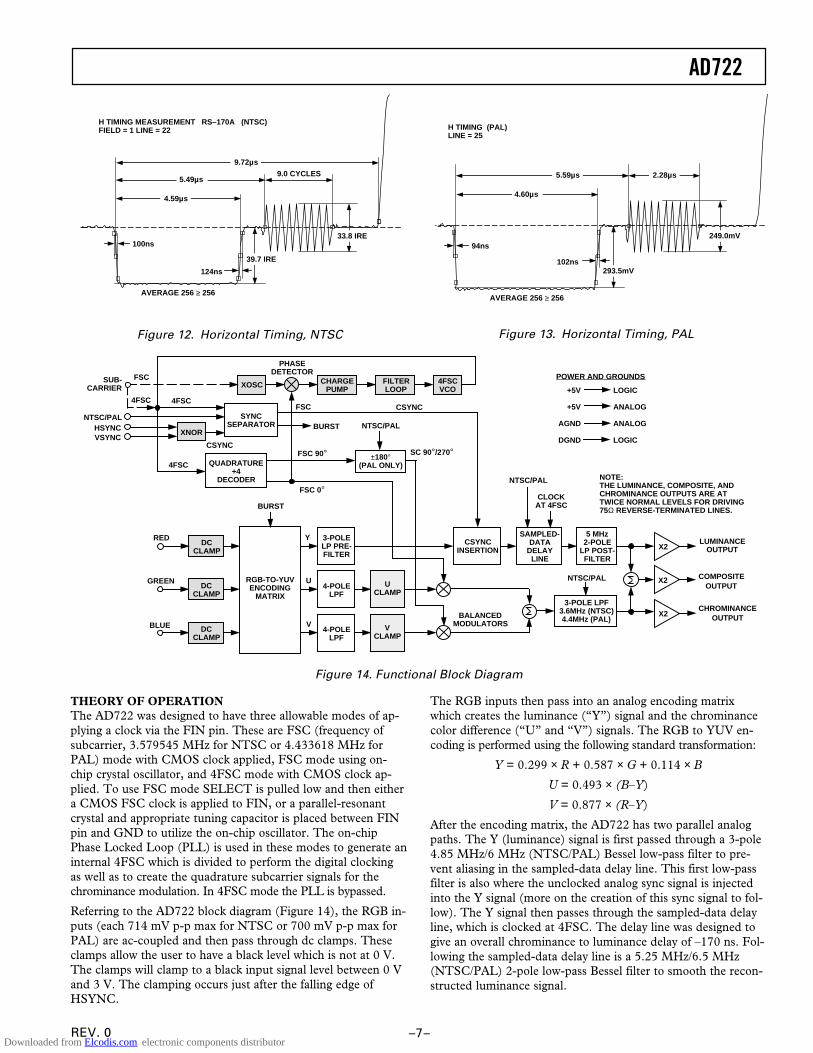
1ST 2ND 3RD 4TH 5TH 6TH
0.00 –0.16 –0.49 –0.53 –0.52 –0.38
0.00 –0.44 –1.14 –1.01 –0.53 –0.01
DG DP (NTSC) (SYNC = EXT)FIELD = 1 LINE = 27, 100 IRE RAMPDIFFERENTIAL GAIN (%)
DIFFERENTIAL PHASE (deg)
MIN = –0.53 MAX = 0.00 p–p/MAX = 0.53
MIN = –1.14 MAX = 0.00 pk–pk = 1.14
0.2
0.0
–0.2
–0.4
–0.6
–0.8
0.5
0.0
–0.5
–1.0
–1.5
Figure 10. Composite Output
Differential Phase and Gain, NTSC
1ST 2ND 3RD 4TH 5TH 6TH
0.00 –0.14 –0.32 –0.16 0.04 0.10
0.00 –1.01 –1.18 –0.44 0.42 0.70
0.30.20.10.0
–0.1–0.2–0.3–0.4–0.5
1.51.00.50.0
–0.5–1.0–1.5–2.0
DG DP (PAL) (SYNC = EXT)LINE = 25, 700mV RAMPDIFFERENTIAL GAIN (%)
DIFFERENTIAL PHASE (deg)
MIN = –0.32 MAX = 0.10 pk–pk = 0.42
MIN = –1.18 MAX = 0.70 pk–pk = 1.89
Figure 11. Composite Output
Differential Phase and Gain, PAL
Figure 7. 100% Color Bars on Vector Scope, PAL
IRE
µs
0.10
0.5
–0.50 6010 20 30 40 50
0.0
VO
LT
S
100
50
0
–50
APL = 11.6%525 LINE NTSC NO FILTERINGSLOW CLAMP TO 0.00V @ 6.63µs
PRECISION MODE OFF SYNCHRONOUS SYNC = SOURCE FRAMES SELECTED : 1 2
Figure 8. Multipulse, NTSC
µs
0.10
0.5
–0.50 6010 20 30 40 50
0.0
VO
LT
S
APL = 11.4%625 LINE PAL NO FILTERINGSLOW CLAMP TO 0.00V @ 6.72µs
PRECISION MODE OFF SOUND-IN-SYNC OFF SYNCHRONOUS SYNC = SOURCE FRAMES SELECTED : 1 2 3 4
Figure 9. Multipulse, PAL
Downloaded from Elcodis.com electronic components distributor
AD722
REV. 0 –7–
9.72µs
5.49µs
4.59µs
39.7 IRE
33.8 IRE
9.0 CYCLES
H TIMING MEASUREMENT RS–170A (NTSC)FIELD = 1 LINE = 22
AVERAGE 256 ≥ 256
124ns
100ns
Figure 12. Horizontal Timing, NTSC
5.59µs
AVERAGE 256 ≥ 256
102ns
94ns
2.28µs
4.60µs
293.5mV
249.0mV
H TIMING (PAL)LINE = 25
Figure 13. Horizontal Timing, PAL
PHASEDETECTOR
CHARGEPUMP
FILTERLOOPXOSC 4FSC
VCO
SYNCSEPARATOR
XNOR
XOSC CHARGEPUMP
FILTERLOOP
4FSCVCO
XNOR
4FSC 4FSC
FSCSUB-CARRIER
NTSC/PALHSYNCVSYNC
BURST
QUADRATURE+4
DECODER
±180°(PAL ONLY)
NTSC/PAL
FSC 90°
FSC 0°
4FSC
SC 90°/270°
FSC CSYNC
CSYNC
DCCLAMP
RED
GREEN
BLUE
RGB-TO-YUVENCODING
MATRIX
BURST
Y 3-POLELP PRE-FILTER
U
V
4-POLELPF
4-POLELPF
BALANCEDMODULATORS
3-POLE LPF3.6MHz (NTSC)4.4MHz (PAL)
NTSC/PAL
CSYNCINSERTION
SAMPLED-DATA
DELAYLINE
5 MHz2-POLE
LP POST-FILTER
X2
X2
X2
LUMINANCEOUTPUT
COMPOSITEOUTPUT
CHROMINANCEOUTPUT
UCLAMP
VCLAMP
NTSC/PAL
CLOCKAT 4FSC
POWER AND GROUNDS
+5V
+5V
AGND
DGND
LOGIC
ANALOG
ANALOG
LOGIC
DCCLAMP
DCCLAMP
NOTE:THE LUMINANCE, COMPOSITE, ANDCHROMINANCE OUTPUTS ARE ATTWICE NORMAL LEVELS FOR DRIVING75Ω REVERSE-TERMINATED LINES.
Figure 14. Functional Block Diagram
THEORY OF OPERATIONThe AD722 was designed to have three allowable modes of ap-plying a clock via the FIN pin. These are FSC (frequency ofsubcarrier, 3.579545 MHz for NTSC or 4.433618 MHz forPAL) mode with CMOS clock applied, FSC mode using on-chip crystal oscillator, and 4FSC mode with CMOS clock ap-plied. To use FSC mode SELECT is pulled low and then eithera CMOS FSC clock is applied to FIN, or a parallel-resonantcrystal and appropriate tuning capacitor is placed between FINpin and GND to utilize the on-chip oscillator. The on-chipPhase Locked Loop (PLL) is used in these modes to generate aninternal 4FSC which is divided to perform the digital clockingas well as to create the quadrature subcarrier signals for thechrominance modulation. In 4FSC mode the PLL is bypassed.
Referring to the AD722 block diagram (Figure 14), the RGB in-puts (each 714 mV p-p max for NTSC or 700 mV p-p max forPAL) are ac-coupled and then pass through dc clamps. Theseclamps allow the user to have a black level which is not at 0 V.The clamps will clamp to a black input signal level between 0 Vand 3 V. The clamping occurs just after the falling edge ofHSYNC.
The RGB inputs then pass into an analog encoding matrixwhich creates the luminance (“Y”) signal and the chrominancecolor difference (“U” and “V”) signals. The RGB to YUV en-coding is performed using the following standard transformation:
Y = 0.299 × R + 0.587 × G + 0.114 × B
U = 0.493 × (B–Y)
V = 0.877 × (R–Y)
After the encoding matrix, the AD722 has two parallel analogpaths. The Y (luminance) signal is first passed through a 3-pole4.85 MHz/6 MHz (NTSC/PAL) Bessel low-pass filter to pre-vent aliasing in the sampled-data delay line. This first low-passfilter is also where the unclocked analog sync signal is injectedinto the Y signal (more on the creation of this sync signal to fol-low). The Y signal then passes through the sampled-data delayline, which is clocked at 4FSC. The delay line was designed togive an overall chrominance to luminance delay of –170 ns. Fol-lowing the sampled-data delay line is a 5.25 MHz/6.5 MHz(NTSC/PAL) 2-pole low-pass Bessel filter to smooth the recon-structed luminance signal.
Downloaded from Elcodis.com electronic components distributor
REV. 0–8–
AD722The other analog path is the chrominance path which is wherethe U and V color difference signals are processed. The U and Vsignals first pass through 4-pole modified Bessel low-pass filterswith –3 dB frequencies of 1.2 MHz/1.5 MHz (NTSC/PAL) toprevent aliasing in the modulators. The color burst signal is in-jected into the U and V channels in these premodulation filters.The U and V signals are then modulated independently by apair of balanced switching modulators driven in quadrature bythe color subcarrier.
The bandwidths of all the on-chip filters are tuned using propri-etary auto-tuning circuitry. The basic principle is to match anRC time constant to a reference time period, that time beingone cycle of a subcarrier clock. The auto-tuning is done duringthe vertical blanking interval and has some added hysteresis sothat once an acceptable tuning value is reached the part won’ttoggle between tuning values from field to field. The band-widths stated in the above discussion are the design target band-widths for NTSC and PAL.
The AD722’s 4FSC clock (either produced by the on-chip PLLor user supplied) drives a digital divide-by-4 circuit to create thequadrature signals for modulation. The reference phase 0° isused for the U signal. In the NTSC mode, the V signal is modu-lated at 90°, but in PAL mode, the V modulation alternates be-tween 90° and 270° at half the line rate as required by the PALstandard. The outputs of the U and V balanced modulatorsare summed and passed through a 3-pole low-pass filter with3.6 MHz/4.4 MHz bandwidths (NTSC/PAL) in order to re-move the harmonics generated during the switching modulation.
The filtered chrominance signal is then summed with the fil-tered luminance signal to create the composite video signal. Theseparate luminance, chrominance, and composite video signalsare amplified by a factor of two in order to drive 75 Ω reverse-terminated lines. The separate luminance and chrominance out-puts together are known as S-video. The composite and S-videooutputs are simultaneously available.
The two sync inputs HSYNC and VSYNC are fed into anXNOR gate to create a CSYNC signal for the AD722. If theuser produces, or has access to, a true composite sync signal, itcan be input to the HSYNC pin while the VSYNC pin is heldhigh. In either case the CSYNC signal which is present after theXNOR gate, is used to generate the sync and burst signalswhich ultimately get injected into the analog signal chain. Theunclocked CSYNC signal is sent to a reference cell on the chipwhich, when CSYNC is low, allows a reference voltage (basedon a power supply division) to be injected into the luminancechain. The width of the injected sync is the same as the width ofthe supplied sync signal.
The CSYNC signal (after the XNOR gate) also goes to the digi-tal section of the AD722 where it is clocked in by a 2FSC clock.The digital section then measures the width of the CSYNCpulses to separate horizontal pulses from vertical equalizing andserration pulses. A burst flag is generated only after valid hori-zontal sync pulses and is timed from the falling edge of theclocked-in CSYNC signal. In synchronous systems (those inwhich the subcarrier clock, sync signals, and RGB signals are allsynchronous) this will give a fixed burst position relative to thefalling edge of the output sync. However, in asynchronous sys-tems the sync to burst position can change line to line by asmuch as 140 ns (the period of a 2FSC clock cycle) due to thefact that the burst flag is generated from a clocked CSYNC whilethe sync is injected unclocked. This phenomenon may or may not
create visual artifacts in some high-end video systems. The burstflag which is generated goes to the reference cell and allows a refer-ence voltage to be inserted to the U and V low-pass filters.
APPLYING THE AD722InputsRIN, BIN, GIN are analog inputs that should be terminated toground with 75 Ω in close proximity to the IC. When properlyterminated the peak-to-peak voltage for a maximum input levelshould be 714 mV p-p for NTSC or 700 mV p-p for PAL. Thehorizontal blanking interval should be the most negative part ofeach signal.
The signal should be flat during the horizontal blanking interval.Internal circuitry will clamp this level during HSYNC to a refer-ence that is used internally as the black level. The horizontalblanking level at the input pins can range between 0 V and 3 Vwith respect to the ground level of the AD722.
HSYNC and VSYNC are two logic level inputs that are com-bined internally to produce a composite sync signal. If a com-posite sync signal is to be used, it can be input to HSYNC whileVSYNC is pulled to logic HI (+5 V).
The form of the input sync signal(s) will determine the form ofthe composite sync on the composite video (COMP) and lumi-nance (LUMA) outputs. If no equalization or serration pulsesare included in the HSYNC input there won’t be any in the out-puts. Although sync signals without equalization and serrationpulses do not technically meet the video standards’ specifica-tions, many monitors do not require these pulses in order todisplay good pictures. The decision whether to include thesesignals is a system tradeoff between cost and complexity andadhering strictly to the video standards.
The SELECT input is a CMOS logic level that programs theAD722 to use a subcarrier at a 1FSC (LO) frequency or a4FSC (HI) frequency for the appropriate standard being used.A 4FSC clock is used directly, while a 1FSC input is multipliedup to 4FSC by an internal phase locked loop.
The FIN input can be a logic level clock at either FSC or 4FSCfrequency or can be a parallel resonant crystal at 1FSC fre-quency. An on-chip oscillator will drive the crystal. Most crys-tals will require a shunt capacitance of between 10 pF and 30pF for reliable start up and proper frequency of operation.
The NTSC specification calls for a frequency accuracy of ±10 Hzfrom the nominal subcarrier frequency of 3.579545 MHz. Whilemaintaining this accuracy in a broadcast studio might not be asevere hardship, it can be quite expensive in a low cost con-sumer application.
The AD722 will operate with subcarrier frequencies that deviatequite far from those specified by the TV standards. However,the monitor will in general not be quite so forgiving. Most moni-tors can tolerate a subcarrier frequency that deviates several hun-dred Hz from the nominal standard without any degradation inpicture quality. These conditions imply that the subcarrier fre-quency accuracy is a system specification and not a specificationof the AD722 itself.
The STND pin is used to select between NTSC and PAL opera-tion. Various blocks inside the AD722 use this input to programtheir operation. Most of the more common variants of NTSCand PAL are supported. There are, however, two known specificstandards which are not supported. These are NTSC 4.43 andM-PAL.
Downloaded from Elcodis.com electronic components distributor
AD722
REV. 0 –9–
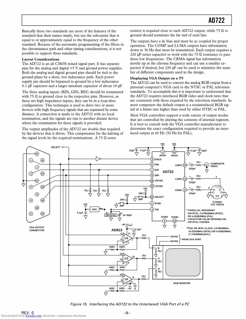
resistor is required close to each AD722 output, while 75 Ω toground should terminate the far end of each line.
The outputs have a dc bias and must be ac coupled for properoperation. The COMP and LUMA outputs have informationdown to 30 Hz that must be transmitted. Each output requires a220 µF series capacitor to work with the 75 Ω resistance to passthese low frequencies. The CRMA signal has informationmostly up at the chroma frequency and can use a smaller ca-pacitor if desired, but 220 µF can be used to minimize the num-ber of different components used in the design.
Displaying VGA Output on a TVThe AD722 can be used to convert the analog RGB output from apersonal computer’s VGA card to the NTSC or PAL televisionstandards. To accomplish this it is important to understand thatthe AD722 requires interlaced RGB video and clock rates thatare consistent with those required by the television standards. Inmost computers the default output is a noninterlaced RGB sig-nal at a frame rate higher than used by either NTSC or PAL.
Most VGA controllers support a wide variety of output modesthat are controlled by altering the contents of internal registers.It is best to consult with the VGA controller manufacturer todetermine the exact configuration required to provide an inter-laced output at 60 Hz (50 Hz for PAL).
Basically these two standards use most of the features of thestandard that their names imply, but use the subcarrier that isequal to or approximately equal to the frequency of the otherstandard. Because of the automatic programming of the filters inthe chrominance path and other timing considerations, it is notpossible to support these standards.
Layout ConsiderationsThe AD722 is an all CMOS mixed signal part. It has separatepins for the analog and digital +5 V and ground power supplies.Both the analog and digital ground pins should be tied to theground plane by a short, low inductance path. Each powersupply pin should be bypassed to ground by a low inductance0.1 µF capacitor and a larger tantalum capacitor of about 10 µF.
The three analog inputs (RIN, GIN, BIN) should be terminatedwith 75 Ω to ground close to the respective pins. However, asthese are high impedance inputs, they can be in a loop-thruconfiguration. This technique is used to drive two or moredevices with high frequency signals that are separated by somedistance. A connection is made to the AD722 with no localtermination, and the signals are run to another distant devicewhere the termination for these signals is provided.
The output amplitudes of the AD722 are double that requiredby the devices that it drives. This compensates for the halving ofthe signal levels by the required terminations. A 75 Ω series
Figure 15. Interfacing the AD722 to the (Interlaced) VGA Port of a PC
+5V (VAA)
0.1µF
75Ω
649Ω649Ω
75Ω
649Ω649Ω
75Ω
649Ω649Ω
AD8135
6 7
11
12
1314
9
108
1/3
1/3
–5V
1
2
34
132
FINOSC0.1µF
+5V
***
CRYSTALAGND DGND
14
15
7
9
10
11
1
4
5
AD722
ENCD
RIN
GIN
BIN
HSYNC
VSYNC
SELECT
STND
CRMA
LUMA
CMPS
APOS DPOS
+
10–30pF
0.1µF 10µF0.1µF10µF
75Ω75Ω
JMP
* PARALLEL–RESONANT CRYSTAL; 3.579545MHz (NTSC) OR 4.433620MHz (PAL) CAPACITOR VALUE DEPENDS ON CRYSTAL CHOSEN
**FSC OR 4FSC CLOCK; 3.579545MHz, 14.31818MHz (NTSC) OR 4.433620MHZ, 17.734480MHz(PAL)
+ 75Ω
220µF
COMPOSITEVIDEO
+ 75Ω
220µF
+ 75Ω
220µF
Y
C
S-VIDEO(Y/C VIDEO)
75Ω
75Ω
75Ω
B
G
R
RGB MONITOR
VSYNC
HSYNCFROM VGA PORT
+5V
+5V
10kΩ+5V
10kΩ
SELECT
75Ω
1/3
JMP
12
3
16
8
6
6
7
8
9
10
11
12
13
14
15
+
+5V
1
2
3
4
5
VGA OUTPUTCONNECTOR
Downloaded from Elcodis.com electronic components distributor
REV. 0–10–
AD722
Figure 15 shows a circuit for connection to the VGA port of aPC. The RGB outputs connect directly to the respective inputsof the AD722. These signals should each be terminated toground with 75 Ω.
The standard 15-pin VGA connector has HSYNC on Pin 13and VSYNC on Pin 14. These signals also connect directly tothe same name signals on the AD722. The FIN signal can beprovided by any of the means described elsewhere in the datasheet. For a synchronous NTSC system, the internal 4FSC(14.31818 MHz) clock that drives the VGA controller can beused for FIN on the AD722. This signal is not directly accessiblefrom outside the computer, but it does appear on the VGA card.
If a separate RGB monitor is also to be used, it is not possible tosimply connect it to the R, G, and B signals. The monitor pro-vides a termination that would double terminate these signals.The R, G, and B signals should be buffered by three amplifierswith high input impedances. These should be configured for again of two, which is normalized by the divide by two termina-tion scheme used for the RGB monitor.
The AD813 is a triple video amplifier that can provide the nec-essary buffering in a single package. It also provides a disablepin for each amplifier which can be used to disable the drive tothe RGB monitor when interlaced video is used (SELECT = LO).When the RGB signals are noninterlaced, setting SELECT HI willenable the AD813 to drive the RGB monitor and disable the en-coding function of the AD722 via Pin 5. HSYNC and VSYNCare logic level signals that can drive both the AD722 and RGBmonitor in parallel.
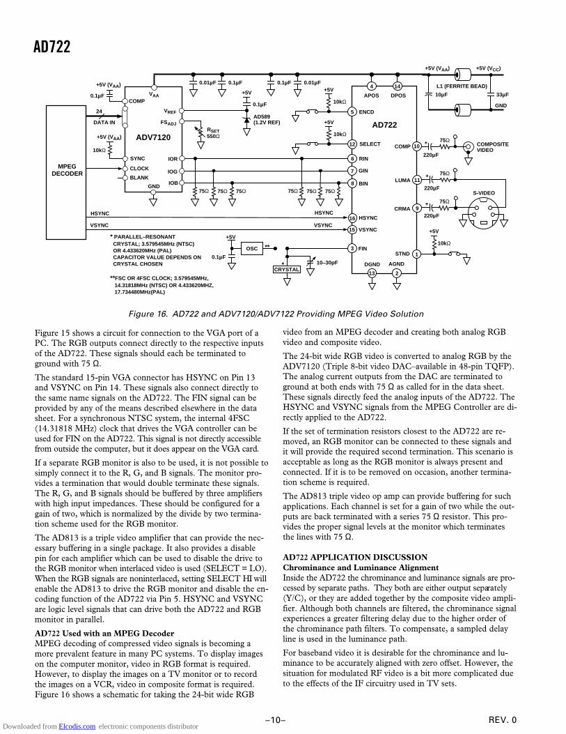
AD722 Used with an MPEG DecoderMPEG decoding of compressed video signals is becoming amore prevalent feature in many PC systems. To display imageson the computer monitor, video in RGB format is required.However, to display the images on a TV monitor or to recordthe images on a VCR, video in composite format is required.Figure 16 shows a schematic for taking the 24-bit wide RGB
video from an MPEG decoder and creating both analog RGBvideo and composite video.
The 24-bit wide RGB video is converted to analog RGB by theADV7120 (Triple 8-bit video DAC–available in 48-pin TQFP).The analog current outputs from the DAC are terminated toground at both ends with 75 Ω as called for in the data sheet.These signals directly feed the analog inputs of the AD722. TheHSYNC and VSYNC signals from the MPEG Controller are di-rectly applied to the AD722.
If the set of termination resistors closest to the AD722 are re-moved, an RGB monitor can be connected to these signals andit will provide the required second termination. This scenario isacceptable as long as the RGB monitor is always present andconnected. If it is to be removed on occasion, another termina-tion scheme is required.
The AD813 triple video op amp can provide buffering for suchapplications. Each channel is set for a gain of two while the out-puts are back terminated with a series 75 Ω resistor. This pro-vides the proper signal levels at the monitor which terminatesthe lines with 75 Ω.
AD722 APPLICATION DISCUSSIONChrominance and Luminance AlignmentInside the AD722 the chrominance and luminance signals are pro-cessed by separate paths. They both are either output separately(Y/C), or they are added together by the composite video ampli-fier. Although both channels are filtered, the chrominance signalexperiences a greater filtering delay due to the higher order ofthe chrominance path filters. To compensate, a sampled delayline is used in the luminance path.
For baseband video it is desirable for the chrominance and lu-minance to be accurately aligned with zero offset. However, thesituation for modulated RF video is a bit more complicated dueto the effects of the IF circuitry used in TV sets.
Figure 16. AD722 and ADV7120/ADV7122 Providing MPEG Video Solution
13 2
FIN
AGNDDGND
15
16 HSYNC
VSYNC
HSYNC
VSYNC
9
COMP+ 75Ω
220µF
COMPOSITEVIDEO
10
11
CRMA
LUMA+ 75Ω
220µF
+ 75Ω
220µF
S-VIDEO
12
1
10kΩ
5
AD722
ENCD
SELECT
STND
APOS DPOS
0.1µF 0.01µF
10–30pF
L1 (FERRITE BEAD)
+5V (VAA)
10µF 33µF
+5V (VCC)
GND
ADV7120
SYNC
CLOCK
BLANK
GND
24
DATA IN
HSYNC
VSYNC
+5V (VAA)
10kΩ
+5V
10kΩ
0.1µF0.01µF
RSET550Ω
0.1µF
+5VVAA
VREF
FSADJ
COMP0.1µF
+5V (VAA)
8
RIN
GIN
BIN75Ω75Ω75Ω
IOG
IOR
IOB
3
MPEGDECODER
6
7
+5V
10kΩ
AD589(1.2V REF)
144
+5V
OSC
0.1µF
+5V
CRYSTAL
75Ω75Ω75Ω
* PARALLEL–RESONANT CRYSTAL; 3.579545MHz (NTSC) OR 4.433620MHz (PAL) CAPACITOR VALUE DEPENDS ON CRYSTAL CHOSEN
**FSC OR 4FSC CLOCK; 3.579545MHz, 14.31818MHz (NTSC) OR 4.433620MHZ, 17.734480MHz(PAL)
**
*
Downloaded from Elcodis.com electronic components distributor
AD722
REV. 0 –11–
The IF strips used in TVs delay the chrominance by 170 nsmore than the luminance. To compensate for this, transmittedvideo has the chrominance lead the luminance by 170 ns. Theterm used for this is chrominance delay, and it is specified as–170 ns, the negative (–) indicating that chrominance leads theluminance. This correction to TV broadcasts was made in theearly days of TV and is the standard to this day.
The delay line used in the luminance path of the AD722 createsa –170 ns chrominance delay. This will be realigned by the RFsection of a TV when it is used for receiving the signal.
However, for baseband inputs, the chrominance will lead theluminance by a small amount. This will show up as a slightcolor shadow to the left of objects. The physical offset can becalculated by approximating the active horizontal line time of aTV as 50 µs. Thus, the chrominance offset distance will be thewidth of the screen times (50 µs/170 ns) or 0.0034. For a 13inch monitor the screen width is about 10 in. (25 cm), so theoffset distance will be 0.034 in. (0.85 mm).
Dot CrawlThere are numerous distortions that are apparent in the presen-tation of composite NTSC signals on TV monitors. These ef-fects will vary in degree depending on the circuitry used by themonitor to process the signal and on the nature of the image be-ing displayed. It is generally not possible to produce pictures ona composite monitor that are as high quality as those producedby standard quality RGB, VGA monitors.
One well known distortion of composite video images is calleddot crawl. It shows up as a moving dot pattern at the interfacebetween two areas of different color. It is caused by the inabilityof the monitor circuitry to adequately separate the luminanceand chrominance signals.
One way to prevent dot crawl is to use a video signal that hasseparate luminance and chrominance. Such a signal is referredto as S-video or Y/C video. Since the luminance and chromi-nance are already separated, the monitor does not have to per-form this function. The S-Video outputs of the AD722 can beused to create higher quality pictures when there is an S-Videoinput available on the monitor.
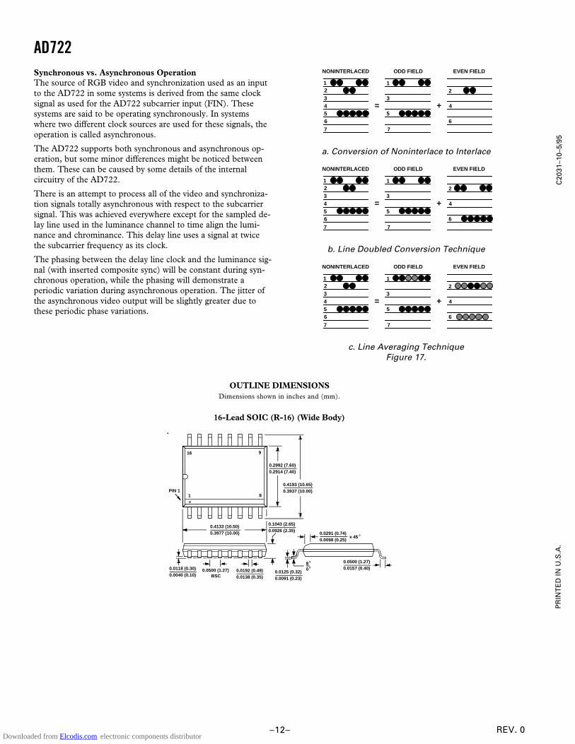
FlickerIn a VGA conversion application, where the software controlledregisters are correctly set, there are two techniques that are com-monly used by VGA controller manufacturers to generate theinterlaced signal. Each of these techniques introduces a uniquecharacteristic into the display created by the AD722. The arti-facts described below are not due to the encoder or its encodingalgorithm as all encoders will generate the same display whenpresented with these inputs. They are due to the method usedby the controller display chip to convert a noninterlaced outputto an interlaced signal. The method used is a feature of the de-sign of the VGA chip and is not programmable.
The first interlacing technique outputs a true interlaced signalwith odd and even fields (one each to a frame Figure 17a). Thisprovides the best picture quality when displaying photography,CD video and animation (games, etc.). However, it will intro-duce a defect commonly referred to as flicker into the display.Flicker is a fundamental defect of all interlaced displays and iscaused by the alternating field characteristic of the interlacetechnique. Consider a one pixel high black line which extendshorizontally across a white screen. This line will exist in only
one field and will be refreshed at a rate of 30 Hz (25 Hz forPAL). During the time that the other field is being displayed theline will not be displayed. The human eye is capable of detect-ing this, and the display will be perceived to have a pulsating orflickering black line. This effect is highly content sensitive andis most pronounced in applications in which text and thinhorizontal lines are present. In applications such as CD video,photography and animation, portions of objects naturallyoccur in both odd and even fields and the effect of flicker isimperceptible.
The second technique which is commonly used is to output an oddand even field which are identical (Figure 17b). This ignores thedata which naturally occurs in one of the fields. In this case thesame one pixel high line mentioned above would either appearas a two pixel high line, (one pixel high in both the odd and evenfield) or will not appear at all if it is in the data which is ignored bythe controller. Which of these cases occurs is dependent on theplacement of the line on the screen. This technique provides astable (i.e., nonflickering) display for all applications, but smalltext can be difficult to read and lines in drawings (or spread-sheets) can disappear. As above, graphics and animation are notparticularly affected although some resolution is lost.
There are methods to dramatically reduce the effect of flicker andmaintain high resolution. The most common is to ensure that dis-play data never exists solely in a single line. This can be accom-plished by averaging/weighting the contents of successive/multiplenoninterlaced lines prior to creating a true interlaced output (Fig-ure 17c). In a sense this provides an output which will lie betweenthe two extremes described above. The weight or percentage of oneline that appears in another and the number of lines used are vari-ables that must be considered in developing a system of this type. Ifthis type of signal processing is performed, it must be completedprior to the data being presented to the AD722 for encoding.
Vertical ScalingIn addition to converting the computer generated image fromnoninterlaced to interlaced format, it is also necessary to scalethe image down to fit into NTSC or PAL format. The mostcommon vertical lines/screen for VGA display are 480 and 600lines. NTSC can only accommodate approximately 400 visiblelines/frame (200 per field), PAL can accommodate 576 lines/frame (288 per field). If scaling is not performed, portions ofthe original image will not appear in the television display.
This line reduction can be performed by merely eliminating ev-ery Nth (6th line in converting 480 lines to NSTC or every 25thline in converting 600 lines to PAL). This risks generation ofjagged edges and jerky movement. It is best to combine the scalingwith the interpolation/averaging technique discussed above toensure that valuable data is not arbitrarily discarded in the scalingprocess. Like the flicker reduction technique mentioned above,the line reduction must be accomplished prior to the AD722 en-coding operation.
There is a new generation of VGA controllers on the marketspecifically designed to utilize these techniques to provide acrisp and stable display for both text and graphics oriented ap-plications. In addition these chips rescale the output from thecomputer to fit correctly on the screen of a television. A list ofknown devices is available through Analog Devices’ Applicationsgroup, but the most complete and current information will beavailable from the manufacturers of graphics controller ICs.
Downloaded from Elcodis.com electronic components distributor
REV. 0–12–
AD722Synchronous vs. Asynchronous OperationThe source of RGB video and synchronization used as an inputto the AD722 in some systems is derived from the same clocksignal as used for the AD722 subcarrier input (FIN). Thesesystems are said to be operating synchronously. In systemswhere two different clock sources are used for these signals, theoperation is called asynchronous.
The AD722 supports both synchronous and asynchronous op-eration, but some minor differences might be noticed betweenthem. These can be caused by some details of the internalcircuitry of the AD722.
There is an attempt to process all of the video and synchroniza-tion signals totally asynchronous with respect to the subcarriersignal. This was achieved everywhere except for the sampled de-lay line used in the luminance channel to time align the lumi-nance and chrominance. This delay line uses a signal at twicethe subcarrier frequency as its clock.
The phasing between the delay line clock and the luminance sig-nal (with inserted composite sync) will be constant during syn-chronous operation, while the phasing will demonstrate aperiodic variation during asynchronous operation. The jitter ofthe asynchronous video output will be slightly greater due tothese periodic phase variations.
C2
03
1–1
0–5
/95
PR
INT
ED
IN
U.S
.A.
12 2
1
3 34 456
56
7 7
= +
NONINTERLACED ODD FIELD EVEN FIELD
a. Conversion of Noninterlace to Interlace
21
34
56
7
= +
NONINTERLACED ODD FIELD EVEN FIELD
123456
7
b. Line Doubled Conversion Technique
21
34
56
7
= +
NONINTERLACED ODD FIELD EVEN FIELD
123456
7
c. Line Averaging Technique
Figure 17.
OUTLINE DIMENSIONSDimensions shown in inches and (mm).
16-Lead SOIC (R-16) (Wide Body)
PIN 1
0.2992 (7.60)0.2914 (7.40)
0.4193 (10.65)0.3937 (10.00)
1
16 9
8
0.0192 (0.49)0.0138 (0.35)
0.0500 (1.27)BSC
0.1043 (2.65)0.0926 (2.35)
0.4133 (10.50) 0.3977 (10.00)
0.0118 (0.30)0.0040 (0.10)
0.0125 (0.32)0.0091 (0.23)
0.0500 (1.27)0.0157 (0.40)
8°0°
0.0291 (0.74)0.0098 (0.25)
x 45°
Downloaded from Elcodis.com electronic components distributor