SAA7114 PAL/NTSC/SECAM video decoder with adaptive · PDF fileThe SAA7114 is a video capture...
144
1. General description The SAA7114 is a video capture device for applications at the image port of Video Graphics Array (VGA) controllers. The SAA7114 is a combination of a two-channel analog preprocessing circuit including source selection, anti-aliasing filter and Analog-to-Digital Converter (ADC), an automatic clamp and gain control, a Clock Generation Circuit (CGC), a digital multistandard decoder containing two-dimensional chrominance/luminance separation by an adaptive comb filter and a high performance scaler, including variable horizontal and vertical up and downscaling and a brightness, contrast and saturation control circuit. It is a highly integrated circuit for desktop video and similar applications. The decoder is based on the principle of line-locked clock decoding and is able to decode the color of PAL, SECAM and NTSC signals into ITU 601 compatible color component values. The SAA7114 accepts CVBS or S-video (Y/C) as analog inputs from TV or VCR sources, including weak and distorted signals. An expansion port (X port) for digital video (bidirectional half duplex, D1 compatible) is also supported to connect to MPEG or a video phone codec. At the so called image port (I port) the SAA7114 supports 8-bit or 16-bit wide output data with auxiliary reference data for interfacing to VGA controllers. The target application for the SAA7114 is to capture and scale video images, to be provided as a digital video stream through the image port of a VGA controller, for display via the frame buffer of the VGA, or for capture to system memory. In parallel the SAA7114 also incorporates provisions for capturing the serially coded data in the Vertical Blanking Interval (VBI) data. Two principal functions are available: 1. To capture raw video samples, after interpolation to the required output data rate, via the scaler 2. A versatile data slicer (data recovery) unit The SAA7114 also incorporates field-locked audio clock generation. This function ensures that there is always the same number of audio samples associated with a field, or a set of fields. This prevents the loss of synchronization between video and audio during capture or playback. The circuit is I 2 C-bus controlled (full write/read capability for all programming registers, bit rate up to 400 kbit/s). SAA7114 PAL/NTSC/SECAM video decoder with adaptive PAL/NTSC comb filter, VBI data slicer and high performance scaler Rev. 03 — 17 January 2006 Product data sheet
Transcript of SAA7114 PAL/NTSC/SECAM video decoder with adaptive · PDF fileThe SAA7114 is a video capture...
1. General description
The SAA7114 is a video capture device for applications at the image port of VideoGraphics Array (VGA) controllers.
The SAA7114 is a combination of a two-channel analog preprocessing circuit includingsource selection, anti-aliasing filter and Analog-to-Digital Converter (ADC), an automaticclamp and gain control, a Clock Generation Circuit (CGC), a digital multistandard decodercontaining two-dimensional chrominance/luminance separation by an adaptive comb filterand a high performance scaler, including variable horizontal and vertical up anddownscaling and a brightness, contrast and saturation control circuit.
It is a highly integrated circuit for desktop video and similar applications. The decoder isbased on the principle of line-locked clock decoding and is able to decode the color ofPAL, SECAM and NTSC signals into ITU 601 compatible color component values. TheSAA7114 accepts CVBS or S-video (Y/C) as analog inputs from TV or VCR sources,including weak and distorted signals. An expansion port (X port) for digital video(bidirectional half duplex, D1 compatible) is also supported to connect to MPEG or a videophone codec. At the so called image port (I port) the SAA7114 supports 8-bit or 16-bitwide output data with auxiliary reference data for interfacing to VGA controllers.
The target application for the SAA7114 is to capture and scale video images, to beprovided as a digital video stream through the image port of a VGA controller, for displayvia the frame buffer of the VGA, or for capture to system memory.
In parallel the SAA7114 also incorporates provisions for capturing the serially coded datain the Vertical Blanking Interval (VBI) data. Two principal functions are available:
1. To capture raw video samples, after interpolation to the required output data rate, viathe scaler
2. A versatile data slicer (data recovery) unit
The SAA7114 also incorporates field-locked audio clock generation. This function ensuresthat there is always the same number of audio samples associated with a field, or a set offields. This prevents the loss of synchronization between video and audio during captureor playback.
The circuit is I2C-bus controlled (full write/read capability for all programming registers, bitrate up to 400 kbit/s).
SAA7114PAL/NTSC/SECAM video decoder with adaptive PAL/NTSCcomb filter, VBI data slicer and high performance scalerRev. 03 — 17 January 2006 Product data sheet

Philips Semiconductors SAA7114PAL/NTSC/SECAM video decoder
2. Features
2.1 Video decoder Six analog inputs, internal analog source selectors, e.g. 6 × CVBS or (2 × Y/C and
2 × CVBS) or (1 × Y/C and 4 × CVBS)
Two analog preprocessing channels in differential CMOS style inclusive built-in analoganti-alias filters
Fully programmable static gain or Automatic Gain Control (AGC) for the selectedCVBS or Y/C channel
Automatic Clamp Control (ACC) for CVBS, Y and C
Switchable white peak control
Two 9-bit video CMOS ADCs, digitized CVBS or Y/C signals are available on theexpansion port
On-chip line-locked clock generation in accordance with “ITU 601” Digital Phase-Locked Loop (PLL) for synchronization and clock generation from all
standards and non-standard video sources e.g. consumer grade VTR
Requires only one crystal (32.11 MHz or 24.576 MHz) for all standards
Horizontal and vertical sync detection
Automatic detection of 50 Hz and 60 Hz field frequency, and automatic switchingbetween PAL and NTSC standards
Luminance and chrominance signal processing for PAL B, G, D, H, I and N,combination PAL N, PAL M, NTSC M, NTSC-Japan, NTSC 4.43 and SECAM
Adaptive 2/4-line comb filter for two dimensional chrominance/luminance separation:
Increased luminance and chrominance bandwidth for all PAL and NTSC standards
Reduced cross color and cross luminance artefacts
PAL delay line for correcting PAL phase errors
Independent Brightness Contrast Saturation (BCS) adjustment for decoder part
User programmable sharpness control
Independent gain and offset adjustment for raw data path
2.2 Video scaler Horizontal and vertical downscaling and upscaling to randomly sized windows
Horizontal and vertical scaling range: variable zoom to 1⁄64 (icon) (it should be notedthat the H and V zoom are restricted by the transfer data rates)
Anti-alias and accumulating filter for horizontal scaling
Vertical scaling with linear phase interpolation and accumulating filter for anti-aliasing(6-bit phase accuracy)
Horizontal phase correct up and downscaling for improved signal quality of scaleddata, especially for compression and video phone applications, with 6-bit phaseaccuracy (1.2 ns step width)
Two independent programming sets for scaler part, to define two ‘ranges’ per field orsequences over frames
Fieldwise switching between decoder part and expansion port (X port) input
Brightness, contrast and saturation controls for scaled outputs
SAA7114_3 © Koninklijke Philips Electronics N.V. 2006. All rights reserved.
Product data sheet Rev. 03 — 17 January 2006 2 of 144
Philips Semiconductors SAA7114PAL/NTSC/SECAM video decoder
2.3 VBI data decoder and slicer Versatile VBI data decoder, slicer, clock regeneration and byte synchronization e.g. for
World Standard Teletext (WST), North American Broadcast Text System (NABTS),closed caption, Wide Screen Signalling (WSS), etc.
2.4 Audio clock generation Generation of a field-locked audio master clock to support a constant number of audio
clocks per video field
Generation of an audio serial and left/right (channel) clock signal
2.5 Digital I/O interfaces Real-time signal port (R port), inclusive continuous line-locked reference clock and
real-time status information supporting RTC level 3.1 (refer to document“RTC Functional Specification” for details)
Bidirectional expansion port (X port) with half duplex functionality (D1), 8-bit Y-CB-CR:
Output from decoder part, real-time and unscaled
Input to scaler part, e.g. video from MPEG decoder (extension to 16-bit possible)
Video image port (I port) configurable for 8-bit data (extension to 16-bit possible) inmaster mode (own clock), or slave mode (external clock), with auxiliary timing andhandshake signals
Discontinuous data streams supported
32-word × 4-byte FIFO register for video output data
28-word × 4-byte FIFO register for decoded VBI data output
Scaled 4 : 2 : 2, 4 : 1 : 1, 4 : 2 : 0, 4 : 1 : 0 Y-CB-CR output
Scaled 8-bit luminance only and raw CVBS data output
Sliced, decoded VBI data output
2.6 Miscellaneous Power-on control
5 V tolerant digital inputs and I/O ports
Software controlled power saving standby modes supported
Programming via serial I2C-bus, full read back ability by an external controller, bit rateup to 400 kbit/s
Boundary scan test circuit complies with the “IEEE Std. 1149.b1 - 1994”
3. Applications
Desktop video
Multimedia
Digital television
Image processing
Video phone applications
SAA7114_3 © Koninklijke Philips Electronics N.V. 2006. All rights reserved.
Product data sheet Rev. 03 — 17 January 2006 3 of 144
Philips Semiconductors SAA7114PAL/NTSC/SECAM video decoder
4. Quick reference data
[1] 8-bit image port output mode, expansion port is 3-stated.
5. Ordering information
Table 1: Quick reference data
Symbol Parameter Conditions Min Typ Max Unit
VDDD digital supply voltage 3.0 3.3 3.6 V
VDDA analog supply voltage 3.1 3.3 3.5 V
Tamb ambient temperature 0 - 70 °C
Ptot(A+D) total power dissipationanalog and digital part
CVBS mode [1] - 0.45 - W
Table 2: Ordering information
Typenumber
Package
Name Description Version
SAA7114E LBGA156 plastic low profile ball grid array package; 156 balls;body 15 × 15 × 1.05 mm
SOT700-1
SAA7114H LQFP100 plastic low profile quad flat package; 100 leads;body 14 × 14 × 1.4 mm
SOT407-1
SAA7114_3 © Koninklijke Philips Electronics N.V. 2006. All rights reserved.
Product data sheet Rev. 03 — 17 January 2006 4 of 144
xxxx xxxxxxxxxxxxxxxxxxxxxxxxxxxxxx x xxxxxxxxxxxxxx xxxxxxxxxx xxx xxxxxx xxxxxxxxxxxxxxxxxxxxxxx xxxxxxxxxxxxxxxxxxxxxxxxxxx xxxxxx xx xxxxxxxxxxxxxxxxxxxxxxxxxxxxx xxxxxxxxxxxxxxxxxxxxxx xxxxxxxxxxx xxxxxxx xxxxxxxxxxxxxxxxxxxxxxxxxxxxxxxxxxx xxxxxxxxxxxxxx xxxxxx xx xxxxxxxxxxxxxxxxxxxxxxxxxxxxxxxx xxxxxxxxxxxxxxxxxxxxxxxx xxxxxxxxxxxxxxxxxxxxxxxxxxxxxxxxxxxxxxxxxxxxxxxxxxxxx xxxxxxxxxxx xxxxx x x
SA
A7114_3
Product data shee
Philips S
emiconduc
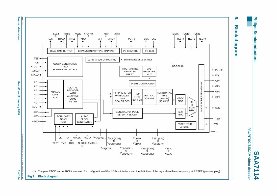
6.B
lock diagram
LLC2 RTS0 XCLK XRV TEST5
4
TEST3
TEST2
TEST1
TEST0
XTRIXPD[7:0]
t
LLC RTCO RTS1 XDQ XRH XRDY SDA SCL TESTHPD[7:0](1)
torsS
AA
7114PA
L/NT
SC
/SE
CA
M video decoder
uency at RESET (pin strapping).
O/TEXTBITER
IMA
GE
PO
RT
PIN
MA
PP
ING
32to
8(16)MUX
ITRI
mhc611
ITRDY
ICLK
IGP1
IGP0
IGPV
IGPH
IDQ
IPD[7:0]
© K
oninklijke Philips E
lectronics N.V. 2006. A
ll rights reserved.
Rev. 03 —
17 January 20065 of 144
(1) The pins RTCO and ALRCLK are used for configuration of the I2C-bus interface and the definition of the crystal oscillator freq
Fig 1. Block diagram
FIR-PREFILTERPRESCALER
ANDSCALER BCS
GENERAL PURPOSEVBI-DATA SLICER
VIDEAR
TEXTFIFO
VIDEOFIFO
PROGRAMMINGREGISTER
ARRAY
A/BREGISTER
MUX
EVENT CONTROLLER
X-PORT I/O FORMATTING
EXPANSION PORT PIN MAPPING I/O CONTROL I2C-BUSREAL-TIME OUTPUT
AI2D
LINEFIFO
BUFFER
VERTICALSCALING
HORIZONTALFINE
(PHASE)SCALING
AGND
AI1D
AOUT
AI24
AI23
AI22
AI21
AI12
AI11
XTALO
XTALI
XTOUT
CE
TCK
TMS
TDI VDD(XTAL)
VSS(XTAL)
VDDD(ICO1)to
VDDD(ICO6)
VDDD(EP1)to
VDDD(EP4)
VDDA0to
VDDA2
VSSD(ICO1)to
VSSD(ICO3)
VSSD(EP1)to
VSSD(EP4)
VSSA0to
VSSA2
AMXCLKTDO
AMCLK
ALRCLK
ASCLK
chrominance of 16-bit input
BOUNDARYSCANTEST
CLOCK GENERATIONAND
POWER-ON CONTROL
ANALOGDUALADC
DIGITALDECODER
WITHADAPTIVE
COMBFILTER
AUDIOCLOCK
GENERATION
RES
SAA7114
TRST(1)
Philips Semiconductors SAA7114PAL/NTSC/SECAM video decoder
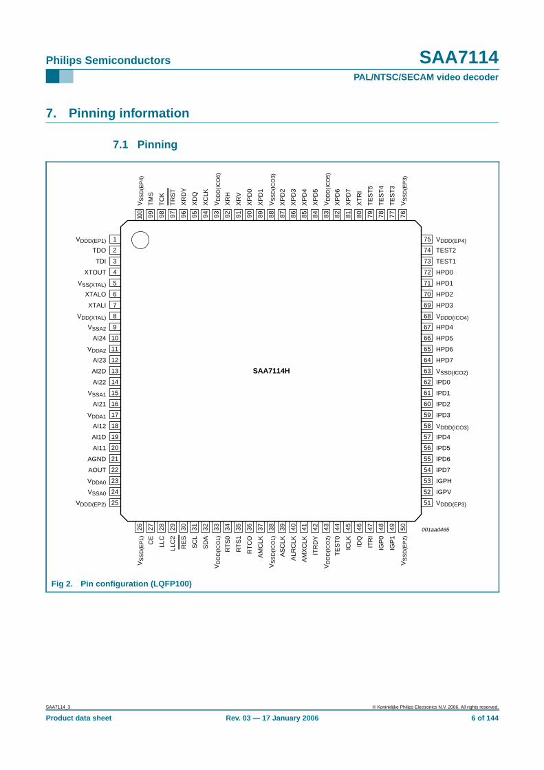
7. Pinning information
7.1 Pinning
Fig 2. Pin configuration (LQFP100)
SAA7114H
VDDD(EP1) VDDD(EP4)
TDO TEST2
TDI TEST1
XTOUT HPD0
VSS(XTAL) HPD1
XTALO HPD2
XTALI HPD3
VDD(XTAL) VDDD(ICO4)
VSSA2 HPD4
AI24 HPD5
VDDA2 HPD6
AI23 HPD7
AI2D VSSD(ICO2)
AI22 IPD0
AI11 IPD5
AGND IPD6
AOUT IPD7
VDDA0 IGPH
VSSA0
VSSA1
AI21
VDDA1
AI12
AI1D
IGPV
IPD1
IPD2
IPD3
VDDD(ICO3)
IPD4
VDDD(EP2) VDDD(EP3)
VS
SD
(EP
1)V
SS
D(E
P4)
CE
TM
S
LLC
TC
K
LLC
2T
RS
T
RE
SX
RD
Y
SC
LX
DQ
SD
AX
CLK
VD
DD
(IC
O1)
VD
DD
(IC
O6)
RT
S0
XR
H
RT
S1
XR
V
RT
CO
XP
D0
AM
CLK
XP
D1
VS
SD
(IC
O1)
VS
SD
(IC
O3)
AS
CLK
XP
D2
ICLK
XP
D7
IDQ
XT
RI
ITR
IT
ES
T5
IGP
0T
ES
T4
IGP
1
ALR
CLK
AM
XC
LK
ITR
DY
VD
DD
(IC
O2)
TE
ST
0
TE
ST
3
XP
D3
XP
D4
XP
D5
VD
DD
(IC
O5)
XP
D6
VS
SD
(EP
2)V
SS
D(E
P3)
001aad465
1
2
3
4
5
6
7
8
9
10
11
12
13
14
20
21
22
23
24
25
75
74
73
72
71
70
69
68
67
66
65
64
63
62
56
55
54
53
52
51
15
16
17
18
19
61
60
59
58
57
26 27 28 29 30 31 32 33 34 35 36 37 38 39 45 46 47 48 49 50
100
99 98 97 96 95 94 93 92 91 90 89 88 87 81 80 79 78 77 76
40 41 42 43 44
86 85 84 83 82
SAA7114_3 © Koninklijke Philips Electronics N.V. 2006. All rights reserved.
Product data sheet Rev. 03 — 17 January 2006 6 of 144
Philips Semiconductors SAA7114PAL/NTSC/SECAM video decoder
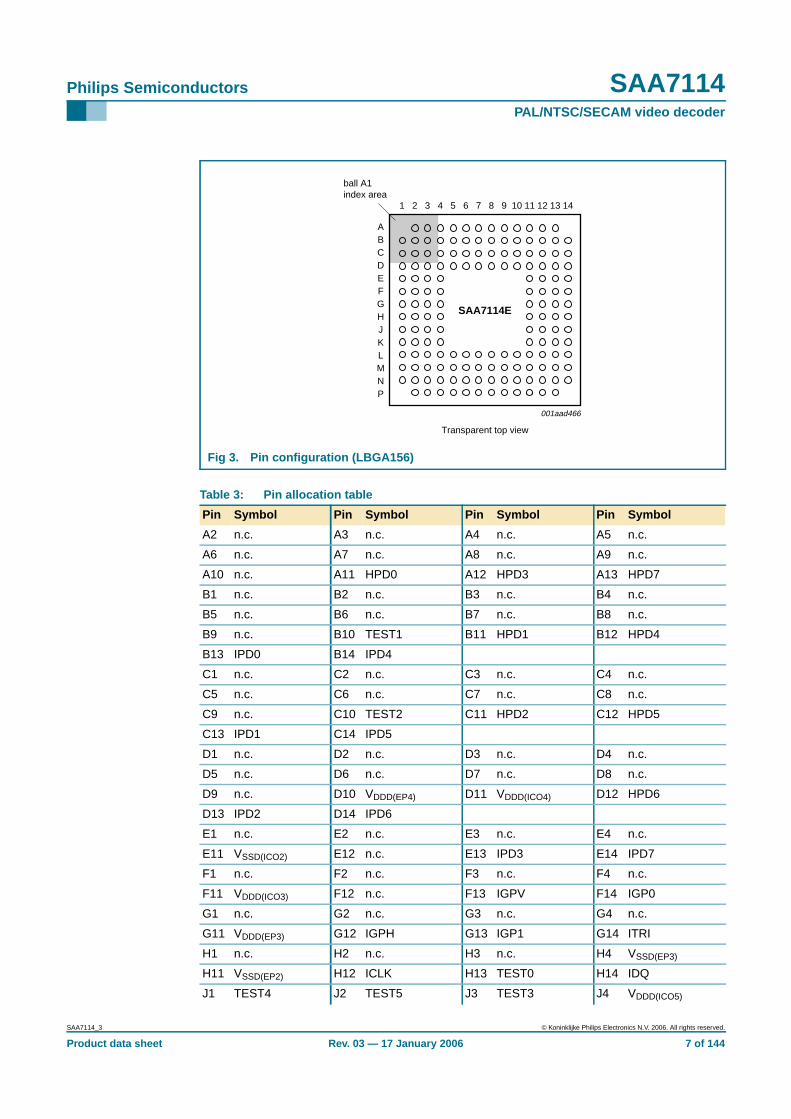
Fig 3. Pin configuration (LBGA156)
Table 3: Pin allocation table
Pin Symbol Pin Symbol Pin Symbol Pin Symbol
A2 n.c. A3 n.c. A4 n.c. A5 n.c.
A6 n.c. A7 n.c. A8 n.c. A9 n.c.
A10 n.c. A11 HPD0 A12 HPD3 A13 HPD7
B1 n.c. B2 n.c. B3 n.c. B4 n.c.
B5 n.c. B6 n.c. B7 n.c. B8 n.c.
B9 n.c. B10 TEST1 B11 HPD1 B12 HPD4
B13 IPD0 B14 IPD4
C1 n.c. C2 n.c. C3 n.c. C4 n.c.
C5 n.c. C6 n.c. C7 n.c. C8 n.c.
C9 n.c. C10 TEST2 C11 HPD2 C12 HPD5
C13 IPD1 C14 IPD5
D1 n.c. D2 n.c. D3 n.c. D4 n.c.
D5 n.c. D6 n.c. D7 n.c. D8 n.c.
D9 n.c. D10 VDDD(EP4) D11 VDDD(ICO4) D12 HPD6
D13 IPD2 D14 IPD6
E1 n.c. E2 n.c. E3 n.c. E4 n.c.
E11 VSSD(ICO2) E12 n.c. E13 IPD3 E14 IPD7
F1 n.c. F2 n.c. F3 n.c. F4 n.c.
F11 VDDD(ICO3) F12 n.c. F13 IGPV F14 IGP0
G1 n.c. G2 n.c. G3 n.c. G4 n.c.
G11 VDDD(EP3) G12 IGPH G13 IGP1 G14 ITRI
H1 n.c. H2 n.c. H3 n.c. H4 VSSD(EP3)
H11 VSSD(EP2) H12 ICLK H13 TEST0 H14 IDQ
J1 TEST4 J2 TEST5 J3 TEST3 J4 VDDD(ICO5)
001aad466
SAA7114E
Transparent top view
PNMLKJ
G
E
H
F
DCBA
2 4 6 8 10 12 13 141 3 5 7 9 11
ball A1index area
SAA7114_3 © Koninklijke Philips Electronics N.V. 2006. All rights reserved.
Product data sheet Rev. 03 — 17 January 2006 7 of 144
Philips Semiconductors SAA7114PAL/NTSC/SECAM video decoder
7.2 Pin description
J11 VDDD(ICO2) J12 AMXCLK J13 ALRCLK J14 ITRDY
K1 XTRI K2 XPD7 K3 XPD6 K4 VSSD(ICO3)
K11 VSSD(ICO1) K12 AMCLK K13 RTS0 K14 ASCLK
L1 XPD5 L2 XPD4 L3 XPD3 L4 VDDD(ICO6)
L5 XRV L6 VSSD(EP4) L7 VDDD(EP1) L8 VDD(XTAL)
L9 VDDD(EP2) L10 RTS1 L11 VDDD(ICO1) L12 SDA
L13 RTCO L14 LLC2
M1 XPD2 M2 XPD1 M3 XCLK M4 XDQ
M5 TMS M6 TCK M7 VSSA2 M8 VDDA2
M9 VDDA1 M10 AOUT M11 SCL M12 RES
M13 VSSD(EP1) M14 LLC
N1 XPD0 N2 XRH N3 XRDY N4 TRST
N5 TDO N6 TDI N7 VSSA2 N8 VSSA1
N9 VSSA1 N10 AGND N11 VDDA0 N12 VSSA0
N13 VSSA0 N14 CE
P2 XTALI P3 XTALO P4 XTOUT P5 VSS(XTAL)
P6 AI24 P7 AI23 P8 AI2D P9 AI22
P10 AI21 P11 AI12 P12 AI1D P13 AI11
Table 3: Pin allocation table …continued
Pin Symbol Pin Symbol Pin Symbol Pin Symbol
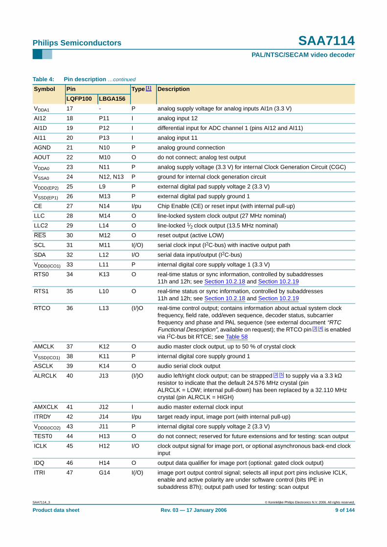
Table 4: Pin description
Symbol Pin Type [1] Description
LQFP100 LBGA156
VDDD(EP1) 1 L7 P external digital pad supply voltage 1 (3.3 V)
TDO 2 N5 O test data output for boundary scan test [2]
TDI 3 N6 I/pu test data input for boundary scan test [2]
XTOUT 4 P4 O crystal oscillator output signal; auxiliary signal
VSS(XTAL) 5 P5 P ground for crystal oscillator
XTALO 6 P3 O 24.576 MHz (32.11 MHz) crystal oscillator output; not connected if TTLclock input of XTALI is used
XTALI 7 P2 I input terminal for 24.576 MHz (32.11 MHz) crystal oscillator or connectionof external oscillator with TTL compatible square wave clock signal
VDD(XTAL) 8 L8 P supply voltage for crystal oscillator
VSSA2 9 M7, N7 P ground for analog inputs AI2n
AI24 10 P6 I analog input 24
VDDA2 11 M8 P analog supply voltage for analog inputs AI2n (3.3 V)
AI23 12 P7 I analog input 23
AI2D 13 P8 I differential input for ADC channel 2 (pins AI24, AI23, AI22 and AI21)
AI22 14 P9 I analog input 22
VSSA1 15 N8, N9 P ground for analog inputs AI1n
AI21 16 P10 I analog input 21
SAA7114_3 © Koninklijke Philips Electronics N.V. 2006. All rights reserved.
Product data sheet Rev. 03 — 17 January 2006 8 of 144
Philips Semiconductors SAA7114PAL/NTSC/SECAM video decoder
VDDA1 17 - P analog supply voltage for analog inputs AI1n (3.3 V)
AI12 18 P11 I analog input 12
AI1D 19 P12 I differential input for ADC channel 1 (pins AI12 and AI11)
AI11 20 P13 I analog input 11
AGND 21 N10 P analog ground connection
AOUT 22 M10 O do not connect; analog test output
VDDA0 23 N11 P analog supply voltage (3.3 V) for internal Clock Generation Circuit (CGC)
VSSA0 24 N12, N13 P ground for internal clock generation circuit
VDDD(EP2) 25 L9 P external digital pad supply voltage 2 (3.3 V)
VSSD(EP1) 26 M13 P external digital pad supply ground 1
CE 27 N14 I/pu Chip Enable (CE) or reset input (with internal pull-up)
LLC 28 M14 O line-locked system clock output (27 MHz nominal)
LLC2 29 L14 O line-locked 1⁄2 clock output (13.5 MHz nominal)
RES 30 M12 O reset output (active LOW)
SCL 31 M11 I(/O) serial clock input (I2C-bus) with inactive output path
SDA 32 L12 I/O serial data input/output (I2C-bus)
VDDD(ICO1) 33 L11 P internal digital core supply voltage 1 (3.3 V)
RTS0 34 K13 O real-time status or sync information, controlled by subaddresses11h and 12h; see Section 10.2.18 and Section 10.2.19
RTS1 35 L10 O real-time status or sync information, controlled by subaddresses11h and 12h; see Section 10.2.18 and Section 10.2.19
RTCO 36 L13 (I/)O real-time control output; contains information about actual system clockfrequency, field rate, odd/even sequence, decoder status, subcarrierfrequency and phase and PAL sequence (see external document “RTCFunctional Description”, available on request); the RTCO pin [3] [4] is enabledvia I2C-bus bit RTCE; see Table 58
AMCLK 37 K12 O audio master clock output, up to 50 % of crystal clock
VSSD(ICO1) 38 K11 P internal digital core supply ground 1
ASCLK 39 K14 O audio serial clock output
ALRCLK 40 J13 (I/)O audio left/right clock output; can be strapped [3] [5] to supply via a 3.3 kΩresistor to indicate that the default 24.576 MHz crystal (pinALRCLK = LOW; internal pull-down) has been replaced by a 32.110 MHzcrystal (pin ALRCLK = HIGH)
AMXCLK 41 J12 I audio master external clock input
ITRDY 42 J14 I/pu target ready input, image port (with internal pull-up)
VDDD(ICO2) 43 J11 P internal digital core supply voltage 2 (3.3 V)
TEST0 44 H13 O do not connect; reserved for future extensions and for testing: scan output
ICLK 45 H12 I/O clock output signal for image port, or optional asynchronous back-end clockinput
IDQ 46 H14 O output data qualifier for image port (optional: gated clock output)
ITRI 47 G14 I(/O) image port output control signal; selects all input port pins inclusive ICLK,enable and active polarity are under software control (bits IPE insubaddress 87h); output path used for testing: scan output
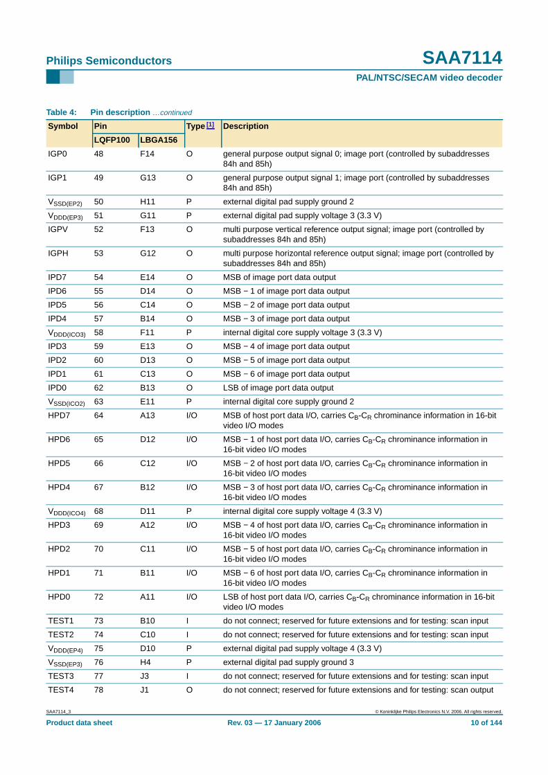
Table 4: Pin description …continued
Symbol Pin Type [1] Description
LQFP100 LBGA156
SAA7114_3 © Koninklijke Philips Electronics N.V. 2006. All rights reserved.
Product data sheet Rev. 03 — 17 January 2006 9 of 144
Philips Semiconductors SAA7114PAL/NTSC/SECAM video decoder
IGP0 48 F14 O general purpose output signal 0; image port (controlled by subaddresses84h and 85h)
IGP1 49 G13 O general purpose output signal 1; image port (controlled by subaddresses84h and 85h)
VSSD(EP2) 50 H11 P external digital pad supply ground 2
VDDD(EP3) 51 G11 P external digital pad supply voltage 3 (3.3 V)
IGPV 52 F13 O multi purpose vertical reference output signal; image port (controlled bysubaddresses 84h and 85h)
IGPH 53 G12 O multi purpose horizontal reference output signal; image port (controlled bysubaddresses 84h and 85h)
IPD7 54 E14 O MSB of image port data output
IPD6 55 D14 O MSB − 1 of image port data output
IPD5 56 C14 O MSB − 2 of image port data output
IPD4 57 B14 O MSB − 3 of image port data output
VDDD(ICO3) 58 F11 P internal digital core supply voltage 3 (3.3 V)
IPD3 59 E13 O MSB − 4 of image port data output
IPD2 60 D13 O MSB − 5 of image port data output
IPD1 61 C13 O MSB − 6 of image port data output
IPD0 62 B13 O LSB of image port data output
VSSD(ICO2) 63 E11 P internal digital core supply ground 2
HPD7 64 A13 I/O MSB of host port data I/O, carries CB-CR chrominance information in 16-bitvideo I/O modes
HPD6 65 D12 I/O MSB − 1 of host port data I/O, carries CB-CR chrominance information in16-bit video I/O modes
HPD5 66 C12 I/O MSB − 2 of host port data I/O, carries CB-CR chrominance information in16-bit video I/O modes
HPD4 67 B12 I/O MSB − 3 of host port data I/O, carries CB-CR chrominance information in16-bit video I/O modes
VDDD(ICO4) 68 D11 P internal digital core supply voltage 4 (3.3 V)
HPD3 69 A12 I/O MSB − 4 of host port data I/O, carries CB-CR chrominance information in16-bit video I/O modes
HPD2 70 C11 I/O MSB − 5 of host port data I/O, carries CB-CR chrominance information in16-bit video I/O modes
HPD1 71 B11 I/O MSB − 6 of host port data I/O, carries CB-CR chrominance information in16-bit video I/O modes
HPD0 72 A11 I/O LSB of host port data I/O, carries CB-CR chrominance information in 16-bitvideo I/O modes
TEST1 73 B10 I do not connect; reserved for future extensions and for testing: scan input
TEST2 74 C10 I do not connect; reserved for future extensions and for testing: scan input
VDDD(EP4) 75 D10 P external digital pad supply voltage 4 (3.3 V)
VSSD(EP3) 76 H4 P external digital pad supply ground 3
TEST3 77 J3 I do not connect; reserved for future extensions and for testing: scan input
TEST4 78 J1 O do not connect; reserved for future extensions and for testing: scan output
Table 4: Pin description …continued
Symbol Pin Type [1] Description
LQFP100 LBGA156
SAA7114_3 © Koninklijke Philips Electronics N.V. 2006. All rights reserved.
Product data sheet Rev. 03 — 17 January 2006 10 of 144
Philips Semiconductors SAA7114PAL/NTSC/SECAM video decoder
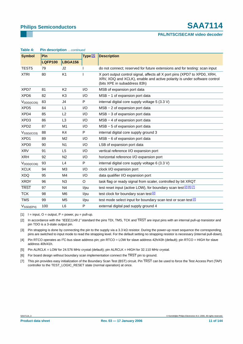
[1] I = input, O = output, P = power, pu = pull-up.
[2] In accordance with the “IEEE1149.1” standard the pins TDI, TMS, TCK and TRST are input pins with an internal pull-up transistor andpin TDO is a 3-state output pin.
[3] Pin strapping is done by connecting the pin to the supply via a 3.3 kΩ resistor. During the power-up reset sequence the correspondingpins are switched to input mode to read the strapping level. For the default setting no strapping resistor is necessary (internal pull-down).
[4] Pin RTCO operates as I2C-bus slave address pin; pin RTCO = LOW for slave address 42h/43h (default); pin RTCO = HIGH for slaveaddress 40h/41h.
[5] Pin ALRCLK = LOW for 24.576 MHz crystal (default); pin ALRCLK = HIGH for 32.110 MHz crystal.
[6] For board design without boundary scan implementation connect the TRST pin to ground.
[7] This pin provides easy initialization of the Boundary Scan Test (BST) circuit. Pin TRST can be used to force the Test Access Port (TAP)controller to the TEST_LOGIC_RESET state (normal operation) at once.
TEST5 79 J2 I do not connect; reserved for future extensions and for testing: scan input
XTRI 80 K1 I X port output control signal, affects all X port pins (XPD7 to XPD0, XRH,XRV, XDQ and XCLK), enable and active polarity is under software control(bits XPE in subaddress 83h)
XPD7 81 K2 I/O MSB of expansion port data
XPD6 82 K3 I/O MSB − 1 of expansion port data
VDDD(ICO5) 83 J4 P internal digital core supply voltage 5 (3.3 V)
XPD5 84 L1 I/O MSB − 2 of expansion port data
XPD4 85 L2 I/O MSB − 3 of expansion port data
XPD3 86 L3 I/O MSB − 4 of expansion port data
XPD2 87 M1 I/O MSB − 5 of expansion port data
VSSD(ICO3) 88 K4 P internal digital core supply ground 3
XPD1 89 M2 I/O MSB − 6 of expansion port data
XPD0 90 N1 I/O LSB of expansion port data
XRV 91 L5 I/O vertical reference I/O expansion port
XRH 92 N2 I/O horizontal reference I/O expansion port
VDDD(ICO6) 93 L4 P internal digital core supply voltage 6 (3.3 V)
XCLK 94 M3 I/O clock I/O expansion port
XDQ 95 M4 I/O data qualifier I/O expansion port
XRDY 96 N3 O task flag or ready signal from scaler, controlled by bit XRQT
TRST 97 N4 I/pu test reset input (active LOW), for boundary scan test [2] [6] [7]
TCK 98 M6 I/pu test clock for boundary scan test [2]
TMS 99 M5 I/pu test mode select input for boundary scan test or scan test [2]
VSSD(EP4) 100 L6 P external digital pad supply ground 4
Table 4: Pin description …continued
Symbol Pin Type [1] Description
LQFP100 LBGA156
SAA7114_3 © Koninklijke Philips Electronics N.V. 2006. All rights reserved.
Product data sheet Rev. 03 — 17 January 2006 11 of 144
xxxxxxxxxxxxxxxxxxxxx xxxxxxxxxxxxxxxxxxxxxxxxxx xxxxxxx x x x xxxxxxxxxxxxxxxxxxxxxxxxxxxxxx xxxxxxxxxxxxxxxxxxx xx xxxxxxx xxxxxxxxxxxxxxxxxxxxxxxxxxx xxxxxxxxxxxxxxxxxxx xxxxxx xxxxxxxxxxxxxxxxxxxxxxxxxxxxxxxxxxx xxxxxxxxxxxx x xxxxxxxxxxxxxxxxxxxxxx xxxxxxxxxxxxxxxxxxxxxxxxxxxxxx xxxxx xxxxxxxxxxxxxxxxxxxxxxxxxxxxxxxxxxxxxxxxxxxxxxxxxx xxxxxxxxxxxxxxxxxxxxxxxxxxxxxxxxx xxxxxxxxxxxxxxxxxxxx xxx
SA
A7114_3
Product data shee
Philips S
emiconductors
SA
A7114
PAL/N
TS
C/S
EC
AM
video decoder
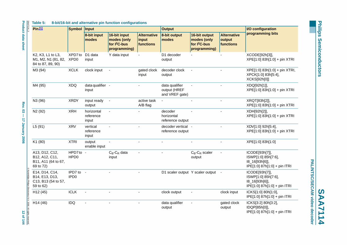
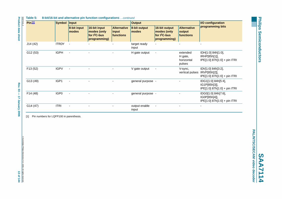
Table 5: 8-bit/16-bit and alternative pin function configurations
Pin [1] Symbol Input Output I/O configurationprogramming bits8-bit input
modes16-bit inputmodes (onlyfor I 2C-bus
Alternativeinputfunctions
8-bit outputmodes
16-bit outputmodes (onlyfor I 2C-bus
Alternativeoutputfunctions
XCODE[92h[3]],XPE[1:0] 83h[1:0] + pin XTRI
XPE[1:0] 83h[1:0] + pin XTRI,XPCK[1:0] 83h[5:4],XCKS[92h[0]]
XDQ[92h[1]],XPE[1:0] 83h[1:0] + pin XTRI
XRQT[83h[2]],XPE[1:0] 83h[1:0] + pin XTRI
XDH[92h[2]],XPE[1:0] 83h[1:0] + pin XTRI
XDV[1:0] 92h[5:4],XPE[1:0] 83h[1:0] + pin XTRI
XPE[1:0] 83h[1:0]
ICODE[93h[7]],ISWP[1:0] 85h[7:6],I8_16[93h[6]],IPE[1:0] 87h[1:0] + pin ITRI
ICODE[93h[7]],ISWP[1:0] 85h[7:6],I8_16[93h[6]],IPE[1:0] 87h[1:0] + pin ITRI
input ICKS[1:0] 80h[1:0],IPE[1:0] 87h[1:0] + pin ITRI
clockt
ICKS[3:2] 80h[3:2],IDQP[85h[0]],IPE[1:0] 87h[1:0] + pin ITRI
© K
oninklijke Philips E
lectronics N.V. 2006. A
ll rights reserved.
tR
ev. 03 — 17 January 2006
12 of 144
programming) programming)
K2, K3, L1 to L3,M1, M2, N1 (81, 82,84 to 87, 89, 90)
XPD7 toXPD0
D1 datainput
Y data input - D1 decoderoutput
- -
M3 (94) XCLK clock input - gated clockinput
decoder clockoutput
- -
M4 (95) XDQ data qualifierinput
- - data qualifieroutput (HREFand VREF gate)
- -
N3 (96) XRDY input readyoutput
- active taskA/B flag
- - -
N2 (92) XRH horizontalreferenceinput
- - decoderhorizontalreference output
- -
L5 (91) XRV verticalreferenceinput
- - decoder verticalreference output
- -
K1 (80) XTRI outputenable input
- - - - -
A13, D12, C12,B12, A12, C11,B11, A11 (64 to 67,69 to 72)
HPD7toHPD0
- CB-CR datainput
- - CB-CR scaleroutput
-
E14, D14, C14,B14, E13, D13,C13, B13 (54 to 57,59 to 62)
IPD7 toIPD0
- - - D1 scaler output Y scaler output -
H12 (45) ICLK - - - clock output - clock
H14 (46) IDQ - - - data qualifieroutput
- gatedoutpu
xxxxxxxxxxxxxxxxxxxxx xxxxxxxxxxxxxxxxxxxxxxxxxx xxxxxxx x x x xxxxxxxxxxxxxxxxxxxxxxxxxxxxxx xxxxxxxxxxxxxxxxxxx xx xxxxxxx xxxxxxxxxxxxxxxxxxxxxxxxxxx xxxxxxxxxxxxxxxxxxx xxxxxx xxxxxxxxxxxxxxxxxxxxxxxxxxxxxxxxxxx xxxxxxxxxxxx x xxxxxxxxxxxxxxxxxxxxxx xxxxxxxxxxxxxxxxxxxxxxxxxxxxxx xxxxx xxxxxxxxxxxxxxxxxxxxxxxxxxxxxxxxxxxxxxxxxxxxxxxxxx xxxxxxxxxxxxxxxxxxxxxxxxxxxxxxxxx xxxxxxxxxxxxxxxxxxxx xxx
SA
A7114_3
Product data shee
Philips S
emiconductors
SA
A7114
PAL/N
TS
C/S
EC
AM
video decoder
-
dede,ontals
IDH[1:0] 84h[1:0],IRHP[85h[1]],IPE[1:0] 87h[1:0] + pin ITRI
c,al pulses
IDV[1:0] 84h[3:2],IRVP[85h[2]],IPE[1:0] 87h[1:0] + pin ITRI
IDG1[1:0] 84h[5:4],IG1P[85h[3]],IPE[1:0] 87h[1:0] + pin ITRI
IDG0[1:0] 84h[7:6],IG0P[85h[4]],IPE[1:0] 87h[1:0] + pin ITRI
-
Table 5: 8-bit/16-bit and alternative pin function configurations …continued
Pin [1] Symbol Input Output I/O configurationprogramming bits8-bit input
modes16-bit inputmodes (onlyfor I 2C-bus
Alternativeinputfunctions
8-bit outputmodes
16-bit outputmodes (onlyfor I 2C-bus
Alternativeoutputfunctions
© K
oninklijke Philips E
lectronics N.V. 2006. A
ll rights reserved.
tR
ev. 03 — 17 January 2006
13 of 144
[1] Pin numbers for LQFP100 in parenthesis.
J14 (42) ITRDY - - - target readyinput
- -
G12 (53) IGPH - - - H gate output - extenH gathorizpulse
F13 (52) IGPV - - - V gate output - V-synvertic
G13 (49) IGP1 - - - general purpose - -
F14 (48) IGP0 - - - general purpose - -
G14 (47) ITRI - - - output enableinput
- -
programming) programming)
Philips Semiconductors SAA7114PAL/NTSC/SECAM video decoder
8. Functional description
8.1 Decoder
8.1.1 Analog input processing
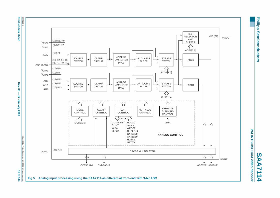
The SAA7114 offers six analog signal inputs, two analog main channels with sourceswitch, clamp circuit, analog amplifier, anti-alias filter and video 9-bit CMOS ADC;see Figure 5.
8.1.2 Analog control circuits
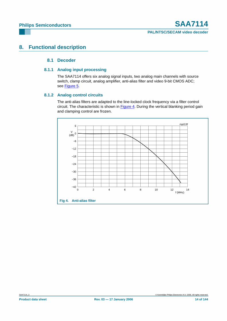
The anti-alias filters are adapted to the line-locked clock frequency via a filter controlcircuit. The characteristic is shown in Figure 4. During the vertical blanking period gainand clamping control are frozen.
Fig 4. Anti-alias filter
f (MHz)0 1242 6 10 148
mgd138
−18
−30
−6
6
0
−12
−24
−36
V(dB)
−42
SAA7114_3 © Koninklijke Philips Electronics N.V. 2006. All rights reserved.
Product data sheet Rev. 03 — 17 January 2006 14 of 144
xxxxxxxxxxxxxxxxxxxxx xxxxxxxxxxxxxxxxxxxxxxxxxx xxxxxxx x x x xxxxxxxxxxxxxxxxxxxxxxxxxxxxxx xxxxxxxxxxxxxxxxxxx xx xxxxxxx xxxxxxxxxxxxxxxxxxxxxxxxxxx xxxxxxxxxxxxxxxxxxx xxxxxx xxxxxxxxxxxxxxxxxxxxxxxxxxxxxxxxxxx xxxxxxxxxxxx x xxxxxxxxxxxxxxxxxxxxxx xxxxxxxxxxxxxxxxxxxxxxxxxxxxxx xxxxx xxxxxxxxxxxxxxxxxxxxxxxxxxxxxxxxxxxxxxxxxxxxxxxxxx xxxxxxxxxxxxxxxxxxxxxxxxxxxxxxxxx xxxxxxxxxxxxxxxxxxxx xxx
SA
A7114_3
Product data shee
Philips S
emiconductors
SA
A7114
PAL/N
TS
C/S
EC
AM
video decoder
ADC2
ADC1
AOSL[1:0]
9 9
AD1BYP
mhc613
AD2BYP
9 9
M10 (22)AOUT
TESTELECTOR
ANDBUFFER
© K
oninklijke Philips E
lectronics N.V. 2006. A
ll rights reserved.
tR
ev. 03 — 17 January 2006
15 of 144
Fig 5. Analog input processing using the SAA7114 as differential front-end with 9-bit ADC
HOLDGGAFIXWPOFFGUDL[1:0]GAI[28:20]GAI[18:10]HLNRSUPTCV
MODE[3:0] HSYGLIMBGLIMTWIPASLTCA
ANALOG CONTROL
VBSL
SOURCESWITCH
CLAMPCIRCUIT
ANALOGAMPLIFIER
DAC9
ANTI-ALIASFILTER
BYPASSSWITCH
SOURCESWITCH
CLAMPCIRCUIT
ANALOGAMPLIFIER
DAC9
ANTI-ALIASFILTER
BYPASSSWITCH
CROSS MULTIPLEXER
VERTICALBLANKINGCONTROL
CLAMPCONTROL
GAINCONTROL
ANTI-ALIASCONTROL
MODECONTROL
FUSE[1:0]
FUSE[1:0]
AGND(21) N10
CVBS/CHRCVBS/LUM
9 9
(18) P11
(19) P12
(20) P13
(15) N8, N9
(9) M7, N7
(13) P8
(10, 12, 14, 16)P6, P7, P9, P10
(17) M9
(11) M8
AI2D
AI12
AI24 to AI21
AI1D
AI11
S
VDDA1
VSSA2
VDDA2
VSSA1
Philips Semiconductors SAA7114PAL/NTSC/SECAM video decoder
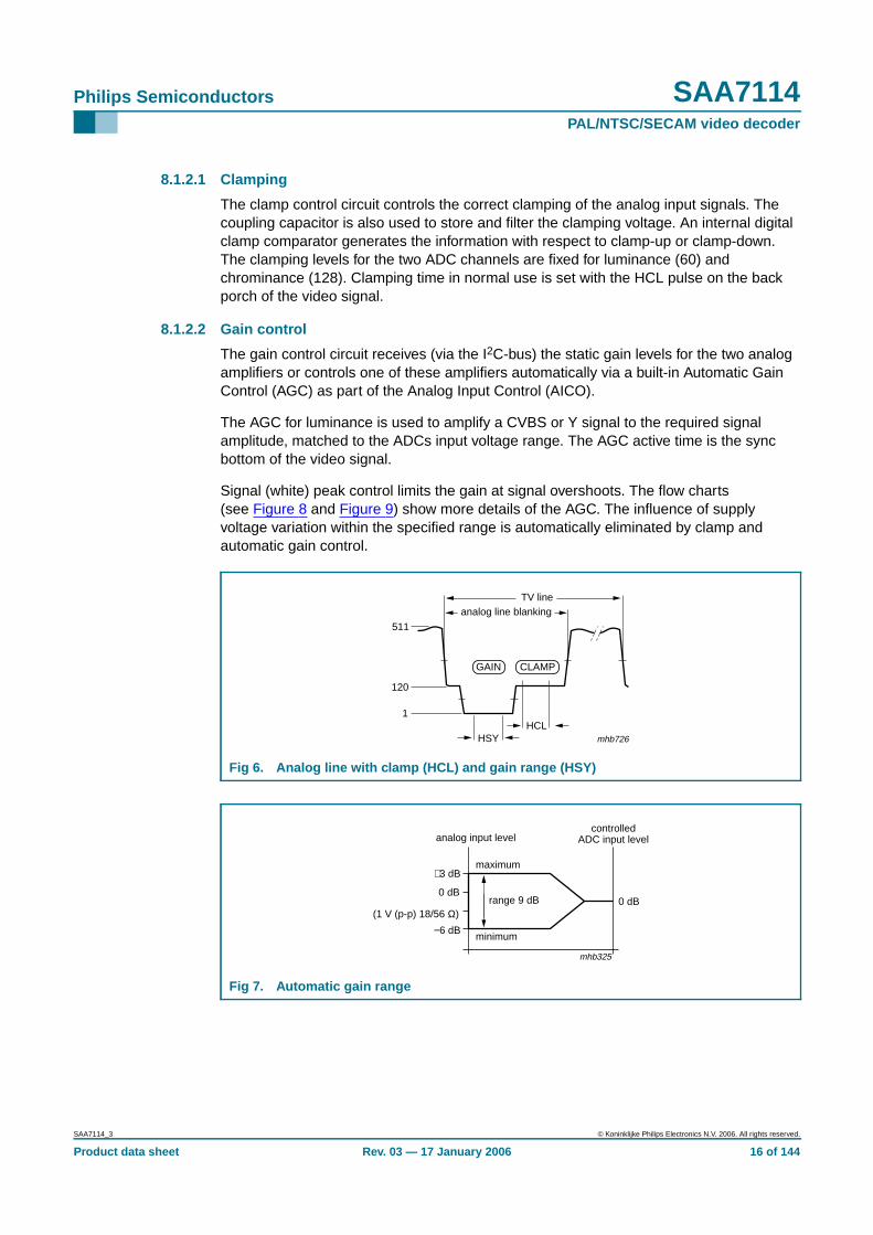
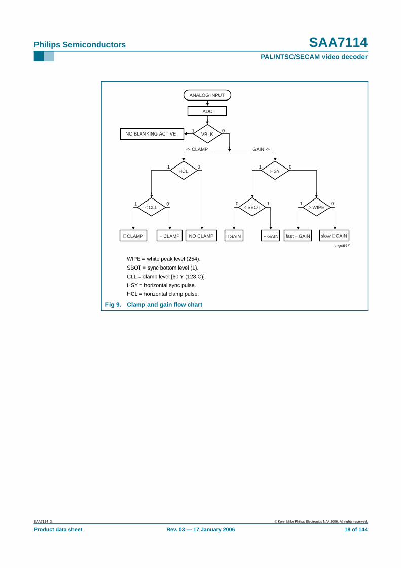
8.1.2.1 Clamping
The clamp control circuit controls the correct clamping of the analog input signals. Thecoupling capacitor is also used to store and filter the clamping voltage. An internal digitalclamp comparator generates the information with respect to clamp-up or clamp-down.The clamping levels for the two ADC channels are fixed for luminance (60) andchrominance (128). Clamping time in normal use is set with the HCL pulse on the backporch of the video signal.
8.1.2.2 Gain control
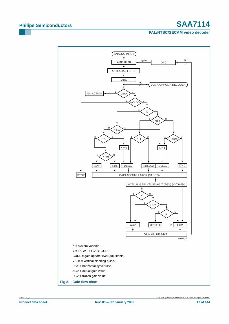
The gain control circuit receives (via the I2C-bus) the static gain levels for the two analogamplifiers or controls one of these amplifiers automatically via a built-in Automatic GainControl (AGC) as part of the Analog Input Control (AICO).
The AGC for luminance is used to amplify a CVBS or Y signal to the required signalamplitude, matched to the ADCs input voltage range. The AGC active time is the syncbottom of the video signal.
Signal (white) peak control limits the gain at signal overshoots. The flow charts(see Figure 8 and Figure 9) show more details of the AGC. The influence of supplyvoltage variation within the specified range is automatically eliminated by clamp andautomatic gain control.
Fig 6. Analog line with clamp (HCL) and gain range (HSY)
Fig 7. Automatic gain range
HCLmhb726HSY
analog line blankingTV line
1
120
511
GAIN CLAMP
analog input levelcontrolled
ADC input level
maximum
minimum
range 9 dB0 dB
0 dB
mhb325
+3 dB
−6 dB
(1 V (p-p) 18/56 Ω)
SAA7114_3 © Koninklijke Philips Electronics N.V. 2006. All rights reserved.
Product data sheet Rev. 03 — 17 January 2006 16 of 144
Philips Semiconductors SAA7114PAL/NTSC/SECAM video decoder
X = system variable.
Y = AGV − FGV > GUDL.
GUDL = gain update level (adjustable).
VBLK = vertical blanking pulse.
HSY = horizontal sync pulse.
AGV = actual gain value.
FGV = frozen gain value.
Fig 8. Gain flow chart
ANALOG INPUT
AMPLIFIER
ANTI-ALIAS FILTER
ADC
LUMA/CHROMA DECODER
X
HSY
> 510
> 510
< 1< 4
> 496
X = 0 X = 1
−1/LLC2 +1/LLC2 −1/LLC2 +/− 0+1/F +1/L
GAIN ACCUMULATOR (18 BITS)
ACTUAL GAIN VALUE 9-BIT (AGV) [−3/+6 dB]
X
STOP
HSY
Y
UPDATE FGV
mhb728
AGV
GAIN VALUE 9-BIT
1 0
1 0
1 0
1 0
1 0
1 0
1 0
1 0
01
10
10
VBLK1 0
NO ACTION
9
9
DACgain
HOLDG
SAA7114_3 © Koninklijke Philips Electronics N.V. 2006. All rights reserved.
Product data sheet Rev. 03 — 17 January 2006 17 of 144
Philips Semiconductors SAA7114PAL/NTSC/SECAM video decoder
WIPE = white peak level (254).
SBOT = sync bottom level (1).
CLL = clamp level [60 Y (128 C)].
HSY = horizontal sync pulse.
HCL = horizontal clamp pulse.
Fig 9. Clamp and gain flow chart
1 0
+ CLAMP − CLAMP NO CLAMP
1 0 1 0
0 1 1 0
mgc647
fast − GAIN slow + GAIN+ GAIN − GAIN
HCL HSY
ADC
< SBOT > WIPE< CLL
ANALOG INPUT
GAIN -><- CLAMP
VBLKNO BLANKING ACTIVE1 0
SAA7114_3 © Koninklijke Philips Electronics N.V. 2006. All rights reserved.
Product data sheet Rev. 03 — 17 January 2006 18 of 144
xxxx xxxxxxxxxxxxxxxxxxxxxxxxxxxxxx x xxxxxxxxxxxxxx xxxxxxxxxx xxx xxxxxx xxxxxxxxxxxxxxxxxxxxxxx xxxxxxxxxxxxxxxxxxxxxxxxxxx xxxxxx xx xxxxxxxxxxxxxxxxxxxxxxxxxxxxx xxxxxxxxxxxxxxxxxxxxxx xxxxxxxxxxx xxxxxxx xxxxxxxxxxxxxxxxxxxxxxxxxxxxxxxxxxx xxxxxxxxxxxxxx xxxxxx xx xxxxxxxxxxxxxxxxxxxxxxxxxxxxxxxx xxxxxxxxxxxxxxxxxxxxxxxx xxxxxxxxxxxxxxxxxxxxxxxxxxxxxxxxxxxxxxxxxxxxxxxxxxxxx xxxxxxxxxxx xxxxx x x
SA
A7114_3
Product data shee
Philips S
emiconduc
8.1.3C
CVBS
t
SUBTRACTORDELAY
COMPENSATION
CVBS-INor Y-IN
CHR
LUMINANCE-PEAKINGOR
LOW-PASS,
Y-DELAY ADJUSTMENT
Y
Y/LDELYCOMB
torsS
AA
7114PA
L/NT
SC
/SE
CA
M video decoder
hrominance and lum
inance processing
mhb729
DCVF
DELAY LINE
SECAMOMBINATION
RI[7:0]ON[7:0]AT[7:0]
G[7:0]O[7:0]
OLO
RIGHTNESSONTRAST
ATURATIONCONTROL
AW DATAGAIN ANDOFFSET
CONTROL
Y-OUT/CVBS OUT
CB-CR-OUT
HREF-OUT
SET_RAWSET_VBI
AWBI
-CR
© K
oninklijke Philips E
lectronics N.V. 2006. A
ll rights reserved.
Rev. 03 —
17 January 200619 of 144 Fig 10. Chrominance and luminance processing
CVBS-INor CHR-IN
CODE BRIG[7:0]CONT[7:0]SATN[7:0]
HUEC[7:0]
QUADRATUREDEMODULATOR
PAL
REC
PHASEDEMODULATOR
AMPLITUDEDETECTOR
BURST GATEACCUMULATOR
LOOP FILTER
LOW-PASS 1DOWNSAMPLING
SUBCARRIERGENERATION 2
FCTCACGC
CGAIN[6:0]IDEL[3:0]RTCO
CB-CRADJUSTMENT
SECAMPROCESSING
fH/2 switch signal
ADAPTIVECOMB FILTER
CCOMBYCOMB
LDELBYPS
LUFI[3:0]CSTD[2:0]YDEL[2:0]
LOW-PASS 2
CHBW
CHROMAGAIN
CONTROL
CB-CR
INTERPOLATIONLOW-PASS 3
LUBW CB-CR
QUADRATUREMODULATOR
CDTOCSTD[2:0]
SUBCARRIERGENERATION 1
CHROMINANCEINCREMENTDTO RESET
SUBCARRIERINCREMENT
GENERATIONAND
DIVIDER
CHROMINANCEINCREMENT
DELAY
LDELYCOMB
CB-CR
LCBW[2:0]
DBDCDSRAWRAW
C
BC
S
R
SET_RAWSET_VBI
SET_RAWSET_VBI
SET_RSET_V
CB
Philips Semiconductors SAA7114PAL/NTSC/SECAM video decoder
8.1.3.1 Chrominance path
The 9-bit CVBS or chrominance input signal is fed to the input of a quadraturedemodulator, where it is multiplied by two time-multiplexed subcarrier signals from thesubcarrier generation block 1 (0° and 90° phase relationship to the demodulator axis).The frequency is dependent on the chosen color standard.
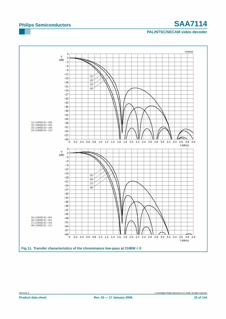
The time-multiplexed output signals of the multipliers are low-pass filtered (low-pass 1).Eight characteristics are programmable via LCBW3 to LCBW0 to achieve the desiredbandwidth for the color difference signals (PAL, NTSC) or the 0° and 90° FM signals(SECAM).
The chrominance low-pass 1 characteristic also influences the grade of cross luminancereduction during horizontal color transients (large chrominance bandwidth means strongsuppression of cross luminance). If the Y-comb filter is disabled by YCOMB = 0 the filterinfluences directly the width of the chrominance notch within the luminance path (a largechrominance bandwidth means wide chrominance notch resulting in a lower luminancebandwidth).
The low-pass filtered signals are fed to the adaptive comb filter block. The chrominancecomponents are separated from the luminance via a two-line vertical stage (four lines forPAL standards) and a decision logic between the filtered and the non-filtered outputsignals. This block is bypassed for SECAM signals. The comb filter logic can be enabledindependently for the succeeding luminance and chrominance processing by YCOMB(subaddress 09h, bit D6) and/or CCOMB (subaddress 0Eh, bit D0). It is always bypassedduring VBI or raw data lines programmable by the LCRn registers (subaddresses41h to 57h); see Section 8.2.
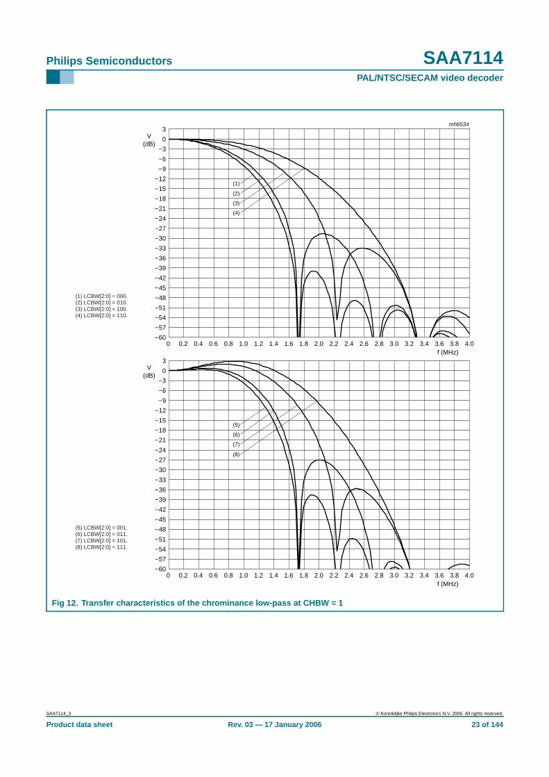
The separated CB-CR components are further processed by a second filter stage(low-pass 2) to modify the chrominance bandwidth without influencing the luminancepath. Its characteristic is controlled by CHBW (subaddress 10h, bit D3). For the completetransfer characteristic of low-passes 1 and 2, see Figure 11 and Figure 12.
The SECAM processing (bypassed for QAM standards) contains the following blocks:
• Baseband ‘bell’ filters to reconstruct the amplitude and phase equalized 0° and 90°FM signals
• Phase demodulator and differentiator (FM-demodulation)
• De-emphasis filter to compensate the pre-emphasized input signal, includingfrequency offset compensation (DB or DR white carrier values are subtracted from thesignal, controlled by the SECAM switch signal)
The succeeding chrominance gain control block amplifies or attenuates the CB-CR signalaccording to the required ITU 601/656 levels. It is controlled by the output signal from theamplitude detection circuit within the burst processing block.
The burst processing block provides the feedback loop of the chrominance PLL andcontains the following:
• Burst gate accumulator
• Color identification and color killer
• Comparison nominal/actual burst amplitude (PAL/NTSC standards only)
• Loop filter chrominance gain control (PAL/NTSC standards only)
SAA7114_3 © Koninklijke Philips Electronics N.V. 2006. All rights reserved.
Product data sheet Rev. 03 — 17 January 2006 20 of 144
Philips Semiconductors SAA7114PAL/NTSC/SECAM video decoder
• Loop filter chrominance PLL (only active for PAL/NTSC standards)
• PAL/SECAM sequence detection, H/2-switch generation
The increment generation circuit produces the Discrete Time Oscillator (DTO) incrementfor both subcarrier generation blocks. It contains a division by the increment of theline-locked clock generator to create a stable phase-locked sine signal under all conditions(e.g. for non-standard signals).
The PAL delay line block eliminates crosstalk between the chrominance channels inaccordance with the PAL standard requirements. For NTSC color standards the delay linecan be used as an additional vertical filter. If desired, it can be switched off by DCVF = 1.It is always disabled during VBI or raw data lines programmable by the LCRn registers(subaddresses 41h to 57h); see Section 8.2. The embedded line delay is also used forSECAM recombination (cross-over switches).
SAA7114_3 © Koninklijke Philips Electronics N.V. 2006. All rights reserved.
Product data sheet Rev. 03 — 17 January 2006 21 of 144
Philips Semiconductors SAA7114PAL/NTSC/SECAM video decoder
Fig 11. Transfer characteristics of the chrominance low-pass at CHBW = 0
mhb533
−60
−57
−54
−51
−48
−45
−42
−39
−36
−33
−30
−27
−24
−21
−18
−15
−12
−9
−6
−3
0
3
0 0.2 0.4 0.6 0.8 1.0 1.2 1.4 1.6 1.8 2.0 2.2 2.4 2.6 2.8 3.0 3.2 3.4 3.6 3.8 4.0
V(dB)
f (MHz)
−60
−57
−54
−51
−48
−45
−42
−39
−36
−33
−30
−27
−24
−21
−18
−15
−12
−9
−6
−3
0
3V
(dB)
0 0.2 0.4 0.6 0.8 1.0 1.2 1.4 1.6 1.8 2.0 2.2 2.4 2.6 2.8 3.0 3.2 3.4 3.6 3.8 4.0f (MHz)
(1)
(2)
(3)
(4)
(5)
(6)
(7)
(8)
(1) LCBW[2:0] = 000.(2) LCBW[2:0] = 010.(3) LCBW[2:0] = 100.(4) LCBW[2:0] = 110.
(5) LCBW[2:0] = 001.(6) LCBW[2:0] = 011.(7) LCBW[2:0] = 101.(8) LCBW[2:0] = 111.
SAA7114_3 © Koninklijke Philips Electronics N.V. 2006. All rights reserved.
Product data sheet Rev. 03 — 17 January 2006 22 of 144
Philips Semiconductors SAA7114PAL/NTSC/SECAM video decoder
Fig 12. Transfer characteristics of the chrominance low-pass at CHBW = 1
mhb534
−60
−57
−54
−51
−48
−45
−42
−39
−36
−33
−30
−27
−24
−21
−18
−15
−12
−9
−6
−3
0
3
0 0.2 0.4 0.6 0.8 1.0 1.2 1.4 1.6 1.8 2.0 2.2 2.4 2.6 2.8 3.0 3.2 3.4 3.6 3.8 4.0
V(dB)
f (MHz)
−60
−57
−54
−51
−48
−45
−42
−39
−36
−33
−30
−27
−24
−21
−18
−15
−12
−9
−6
−3
0
3V
(dB)
0 0.2 0.4 0.6 0.8 1.0 1.2 1.4 1.6 1.8 2.0 2.2 2.4 2.6 2.8 3.0 3.2 3.4 3.6 3.8 4.0f (MHz)
(1)
(2)
(3)
(4)
(5)
(6)
(7)
(8)
(1) LCBW[2:0] = 000.(2) LCBW[2:0] = 010.(3) LCBW[2:0] = 100.(4) LCBW[2:0] = 110.
(5) LCBW[2:0] = 001.(6) LCBW[2:0] = 011.(7) LCBW[2:0] = 101.(8) LCBW[2:0] = 111.
SAA7114_3 © Koninklijke Philips Electronics N.V. 2006. All rights reserved.
Product data sheet Rev. 03 — 17 January 2006 23 of 144
Philips Semiconductors SAA7114PAL/NTSC/SECAM video decoder
8.1.3.2 Luminance path
The rejection of the chrominance components within the 9-bit CVBS or Y input signal isachieved by subtracting the remodulated chrominance signal from the CVBS input.
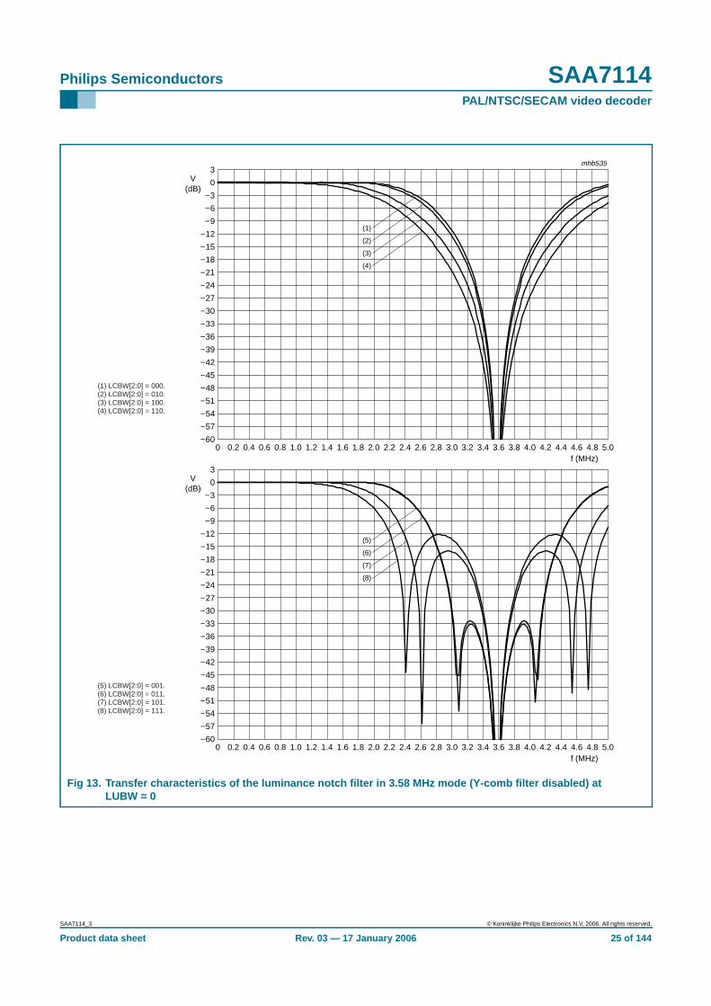
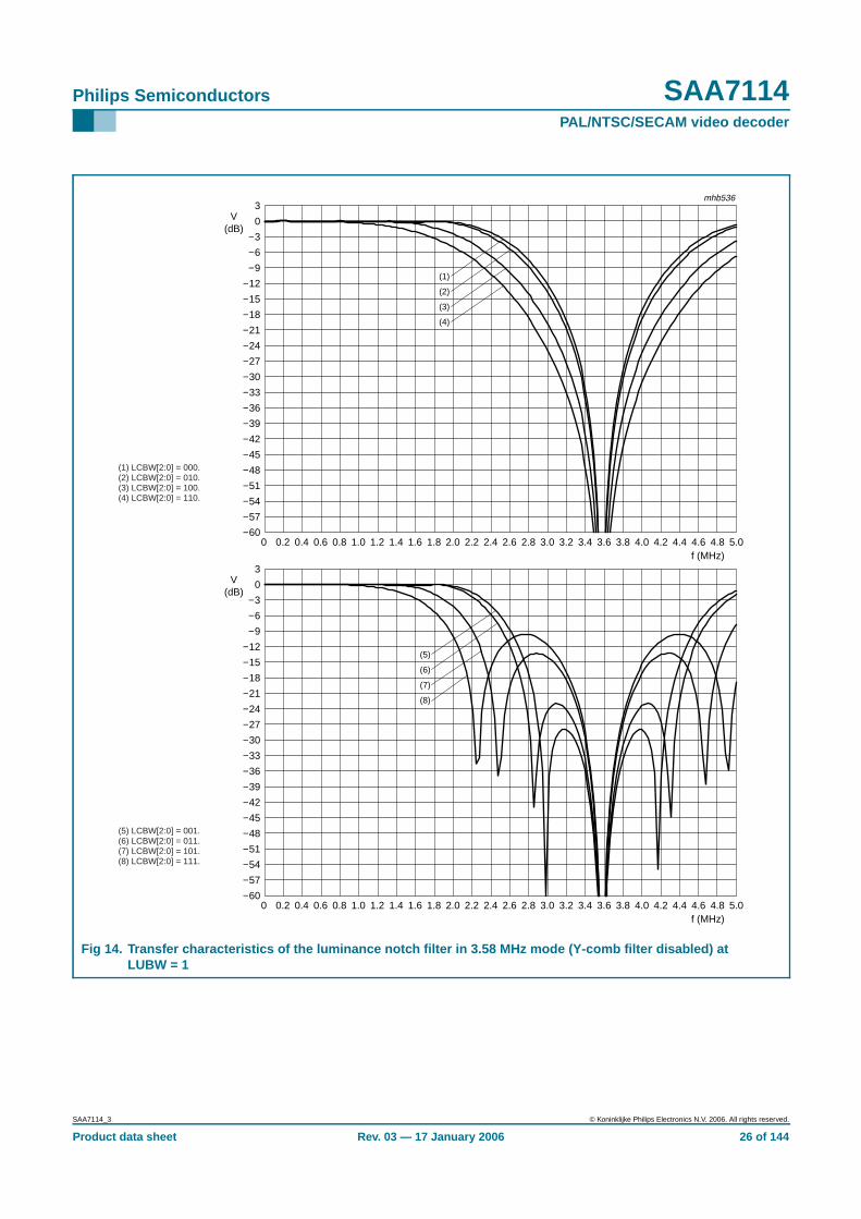
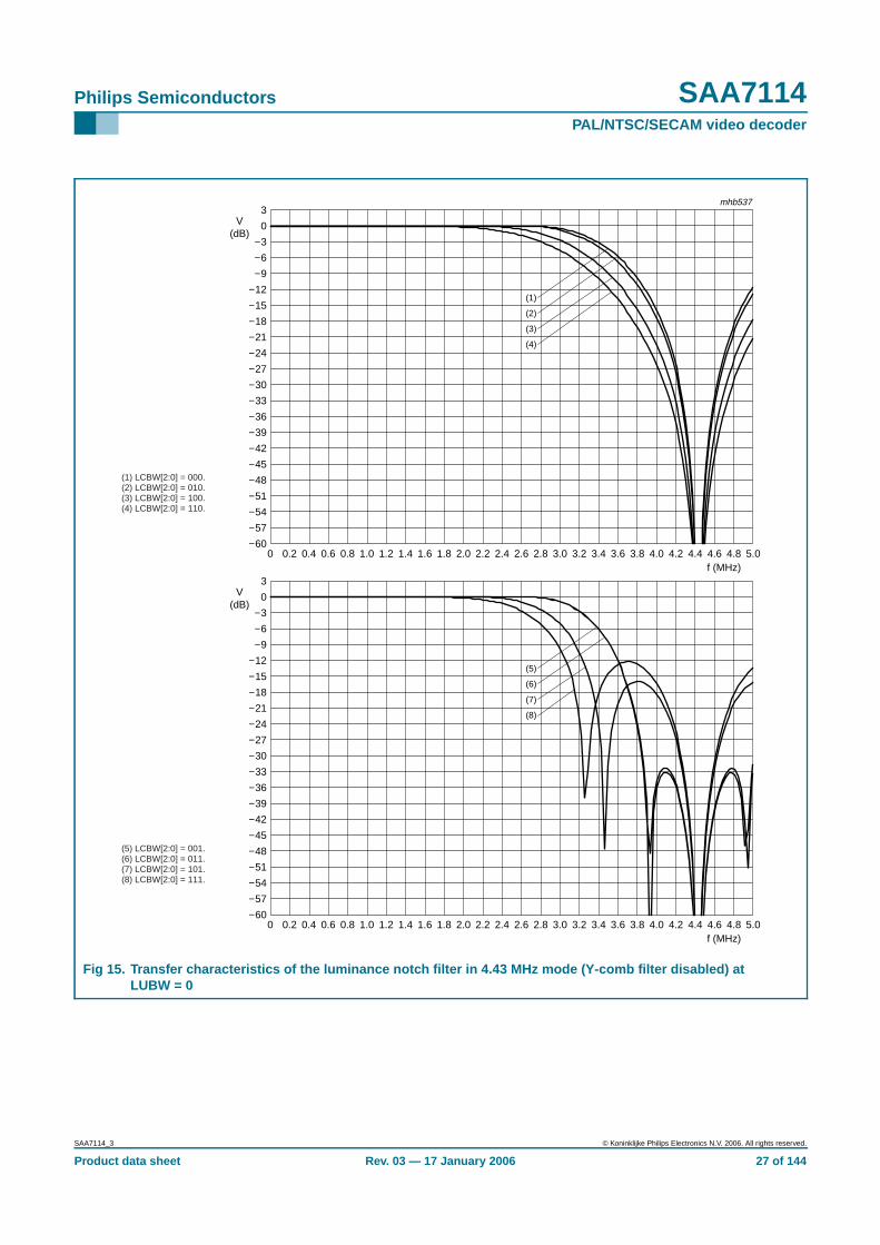
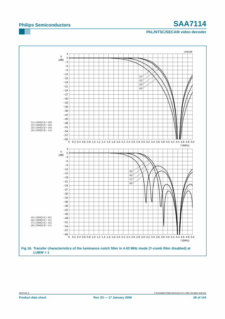
The comb filtered CB-CR components are interpolated (upsampled) by the low-pass 3block. Its characteristic is controlled by LUBW (subaddress 09h, bit D4) to modify thewidth of the chrominance ‘notch’ without influencing the chrominance path. Theprogrammable frequency characteristics available, in conjunction with the LCBW2 toLCBW0 settings, can be seen in Figure 13 to Figure 16. It should be noted that thesefrequency curves are only valid for Y-comb disabled filter mode (YCOMB = 0). In combfilter mode the frequency response is flat. The center frequency of the notch isautomatically adapted to the chosen color standard.
The interpolated CB-CR samples are multiplied by two time-multiplexed subcarrier signalsfrom the subcarrier generation block 2. This second DTO is locked to the first subcarriergenerator by an increment delay circuit matched to the processing delay, which is differentfor PAL and NTSC standards according to the chosen comb filter algorithm. The twomodulated signals are finally added to build the remodulated chrominance signal.
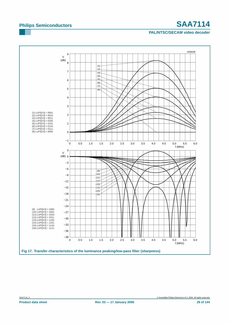
The frequency characteristic of the separated luminance signal can be further modified bythe succeeding luminance filter block. It can be configured as peaking (resolutionenhancement) or low-pass block by LUFI3 to LUFI0 (subaddress 09h, bits D3 to D0). The16 resulting frequency characteristics can be seen in Figure 17. The LUFI3 to LUFI0settings can be used as a user programmable sharpness control.
The luminance filter block also contains the adjustable Y-delay part; programmable byYDEL2 to YDEL0 (subaddress 11h, bits D2 to D0).
SAA7114_3 © Koninklijke Philips Electronics N.V. 2006. All rights reserved.
Product data sheet Rev. 03 — 17 January 2006 24 of 144
Philips Semiconductors SAA7114PAL/NTSC/SECAM video decoder
Fig 13. Transfer characteristics of the luminance notch filter in 3.58 MHz mode (Y-comb filter disabled) atLUBW = 0
mhb535
−60
−57
−54
−51
−48
−45
−42
−39
−36
−33
−30
−27
−24
−21
−18
−15
−12
−9
−6
−3
0
3
0 0.2 0.4 0.6 0.8 1.0 1.2 1.4 1.6 1.8 2.0 2.2 2.4 2.6 2.8 3.0 3.2 3.4 3.6 3.8 4.0 4.2 4.4 4.6 4.8 5.0
V(dB)
f (MHz)
−60
−57
−54
−51
−48
−45
−42
−39
−36
−33
−30
−27
−24
−21
−18
−15
−12
−9
−6
−3
0
3
0 0.2 0.4 0.6 0.8 1.0 1.2 1.4 1.6 1.8 2.0 2.2 2.4 2.6 2.8 3.0 3.2 3.4 3.6 3.8 4.0 4.2 4.4 4.6 4.8 5.0
V(dB)
f (MHz)
(5)
(6)
(7)
(8)
(1)
(2)
(3)
(4)
(1) LCBW[2:0] = 000.(2) LCBW[2:0] = 010.(3) LCBW[2:0] = 100.(4) LCBW[2:0] = 110.
(5) LCBW[2:0] = 001.(6) LCBW[2:0] = 011.(7) LCBW[2:0] = 101.(8) LCBW[2:0] = 111.
SAA7114_3 © Koninklijke Philips Electronics N.V. 2006. All rights reserved.
Product data sheet Rev. 03 — 17 January 2006 25 of 144
Philips Semiconductors SAA7114PAL/NTSC/SECAM video decoder
Fig 14. Transfer characteristics of the luminance notch filter in 3.58 MHz mode (Y-comb filter disabled) atLUBW = 1
mhb536
0 0.2 0.4 0.6 0.8 1.0 1.2 1.4 1.6 1.8 2.0 2.2 2.4 2.6 2.8 3.0 3.2 3.4 3.6 3.8 4.0 4.2 4.4 4.6 4.8 5.0−60
−57
−54
−51
−48
−45
−42
−39
−36
−33
−30
−27
−24
−21
−18
−15
−12
−9
−6
−3
0
3V
(dB)
f (MHz)
−60
−57
−54
−51
−48
−45
−42
−39
−36
−33
−30
−27
−24
−21
−18
−15
−12
−9
−6
−3
0
3
0 0.2 0.4 0.6 0.8 1.0 1.2 1.4 1.6 1.8 2.0 2.2 2.4 2.6 2.8 3.0 3.2 3.4 3.6 3.8 4.0 4.2 4.4 4.6 4.8 5.0
V(dB)
f (MHz)
(5)
(6)
(7)
(8)
(1)
(2)
(3)
(4)
(1) LCBW[2:0] = 000.(2) LCBW[2:0] = 010.(3) LCBW[2:0] = 100.(4) LCBW[2:0] = 110.
(5) LCBW[2:0] = 001.(6) LCBW[2:0] = 011.(7) LCBW[2:0] = 101.(8) LCBW[2:0] = 111.
SAA7114_3 © Koninklijke Philips Electronics N.V. 2006. All rights reserved.
Product data sheet Rev. 03 — 17 January 2006 26 of 144
Philips Semiconductors SAA7114PAL/NTSC/SECAM video decoder
Fig 15. Transfer characteristics of the luminance notch filter in 4.43 MHz mode (Y-comb filter disabled) atLUBW = 0
mhb537
−60
−57
−54
−51
−48
−45
−42
−39
−36
−33
−30
−27
−24
−21
−18
−15
−12
−9
−6
−3
0
3
0 0.2 0.4 0.6 0.8 1.0 1.2 1.4 1.6 1.8 2.0 2.2 2.4 2.6 2.8 3.0 3.2 3.4 3.6 3.8 4.0 4.2 4.4 4.6 4.8 5.0
V(dB)
f (MHz)
−60
−57
−54
−51
−48
−45
−42
−39
−36
−33
−30
−27
−24
−21
−18
−15
−12
−9
−6
−3
0
3
0 0.2 0.4 0.6 0.8 1.0 1.2 1.4 1.6 1.8 2.0 2.2 2.4 2.6 2.8 3.0 3.2 3.4 3.6 3.8 4.0 4.2 4.4 4.6 4.8 5.0
V(dB)
f (MHz)
(5)
(6)
(7)
(8)
(1)
(2)
(3)
(4)
(1) LCBW[2:0] = 000.(2) LCBW[2:0] = 010.(3) LCBW[2:0] = 100.(4) LCBW[2:0] = 110.
(5) LCBW[2:0] = 001.(6) LCBW[2:0] = 011.(7) LCBW[2:0] = 101.(8) LCBW[2:0] = 111.
SAA7114_3 © Koninklijke Philips Electronics N.V. 2006. All rights reserved.
Product data sheet Rev. 03 — 17 January 2006 27 of 144
Philips Semiconductors SAA7114PAL/NTSC/SECAM video decoder
Fig 16. Transfer characteristics of the luminance notch filter in 4.43 MHz mode (Y-comb filter disabled) atLUBW = 1
mhb538
−60
−57
−54
−51
−48
−45
−42
−39
−36
−33
−30
−27
−24
−21
−18
−15
−12
−9
−6
−3
0
3
0 0.2 0.4 0.6 0.8 1.0 1.2 1.4 1.6 1.8 2.0 2.2 2.4 2.6 2.8 3.0 3.2 3.4 3.6 3.8 4.0 4.2 4.4 4.6 4.8 5.0
V(dB)
f (MHz)
−60
−57
−54
−51
−48
−45
−42
−39
−36
−33
−30
−27
−24
−21
−18
−15
−12
−9
−6
−3
0
3
0 0.2 0.4 0.6 0.8 1.0 1.2 1.4 1.6 1.8 2.0 2.2 2.4 2.6 2.8 3.0 3.2 3.4 3.6 3.8 4.0 4.2 4.4 4.6 4.8 5.0
V(dB)
f (MHz)
(5)
(6)
(7)
(8)
(1)
(2)
(3)
(4)
(1) LCBW[2:0] = 000.(2) LCBW[2:0] = 010.(3) LCBW[2:0] = 100.(4) LCBW[2:0] = 110.
(5) LCBW[2:0] = 001.(6) LCBW[2:0] = 011.(7) LCBW[2:0] = 101.(8) LCBW[2:0] = 111.
SAA7114_3 © Koninklijke Philips Electronics N.V. 2006. All rights reserved.
Product data sheet Rev. 03 — 17 January 2006 28 of 144
Philips Semiconductors SAA7114PAL/NTSC/SECAM video decoder
Fig 17. Transfer characteristics of the luminance peaking/low-pass filter (sharpness)
mhb539
−1
0
1
2
3
4
5
6
7
8
9V
(dB)
V(dB)
f (MHz)0 0.5 1.0 1.5 2.0 2.5 3.0 3.5 4.0 4.5 5.0 5.5 6.0
f (MHz)0 0.5 1.0 1.5 2.0 2.5 3.0 3.5 4.0 4.5 5.0 5.5 6.0
(8)
(7)
(6)
(5)
(4)
(3)
(2)
(1)
(9)
(10)
(11)
(12)
(13)
(14)
(15)
(16)
−39
−36
−33
−30
−27
−24
−21
−18
−15
−12
−9
−6
−3
0
3
(1) LUFI[3:0] = 0001.(2) LUFI[3:0] = 0010.(3) LUFI[3:0] = 0011.(4) LUFI[3:0] = 0100.(5) LUFI[3:0] = 0101.(6) LUFI[3:0] = 0110.(7) LUFI[3:0] = 0111.(8) LUFI[3:0] = 0000.
(9) LUFI[3:0] = 1000.(10) LUFI[3:0] = 1001.(11) LUFI[3:0] = 1010.(12) LUFI[3:0] = 1011.(13) LUFI[3:0] = 1100.(14) LUFI[3:0] = 1101.(15) LUFI[3:0] = 1110.(16) LUFI[3:0] = 1111.
SAA7114_3 © Koninklijke Philips Electronics N.V. 2006. All rights reserved.
Product data sheet Rev. 03 — 17 January 2006 29 of 144
Philips Semiconductors SAA7114PAL/NTSC/SECAM video decoder
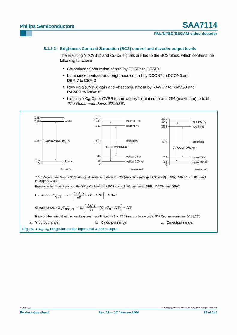
8.1.3.3 Brightness Contrast Saturation (BCS) control and decoder output levels
The resulting Y (CVBS) and CB-CR signals are fed to the BCS block, which contains thefollowing functions:
• Chrominance saturation control by DSAT7 to DSAT0
• Luminance contrast and brightness control by DCON7 to DCON0 andDBRI7 to DBRI0
• Raw data (CVBS) gain and offset adjustment by RAWG7 to RAWG0 andRAWO7 to RAWO0
• Limiting Y-CB-CR or CVBS to the values 1 (minimum) and 254 (maximum) to fulfil“ITU Recommendation 601/656”.
“ITU Recommendation 601/656” digital levels with default BCS (decoder) settings DCON[7:0] = 44h, DBRI[7:0] = 80h andDSAT[7:0] = 40h.
Equations for modification to the Y-CB-CR levels via BCS control I2C-bus bytes DBRI, DCON and DSAT.
Luminance:
Chrominance:
It should be noted that the resulting levels are limited to 1 to 254 in accordance with “ITU Recommendation 601/656”.
a. Y output range. b. CB output range. c. CR output range.
Fig 18. Y-CB-CR range for scaler input and X port output
001aac241
+128 LUMINANCE 100 %
+160
+235
black
white+255
001aac480
+255
+212
+128
0
CB-COMPONENT
+44
+240
+16
blue 100 %
blue 75 %
yellow 75 %
yellow 100 %
colorless
001aac481
+255
+212
+128
0
CR-COMPONENT
+44
+240
+16
red 100 %
red 75 %
cyan 75 %
cyan 100 %
colorless
YOUT IntDCON
68------------------ Y 128–( )× DBRI+=
CRCB( )OUT
IntDSAT
64--------------- CR CB 128–( , )× 128+=
SAA7114_3 © Koninklijke Philips Electronics N.V. 2006. All rights reserved.
Product data sheet Rev. 03 — 17 January 2006 30 of 144
Philips Semiconductors SAA7114PAL/NTSC/SECAM video decoder
8.1.4 Synchronization
The prefiltered luminance signal is fed to the synchronization stage. Its bandwidth isfurther reduced to 1 MHz in a low-pass filter. The sync pulses are sliced and fed to thephase detectors where they are compared with the sub-divided clock frequency. Theresulting output signal is applied to the loop filter to accumulate all phase deviations.Internal signals (e.g. HCL and HSY) are generated in accordance with analog front-endrequirements. The loop filter signal drives an oscillator to generate the line frequencycontrol signal LFCO; see Figure 20.
The detection of ‘pseudo syncs’ as part of the Macrovision copy protection standard isalso achieved within the synchronization circuit.
The result is reported as flag COPRO within the decoder status byte at subaddress 1Fh.
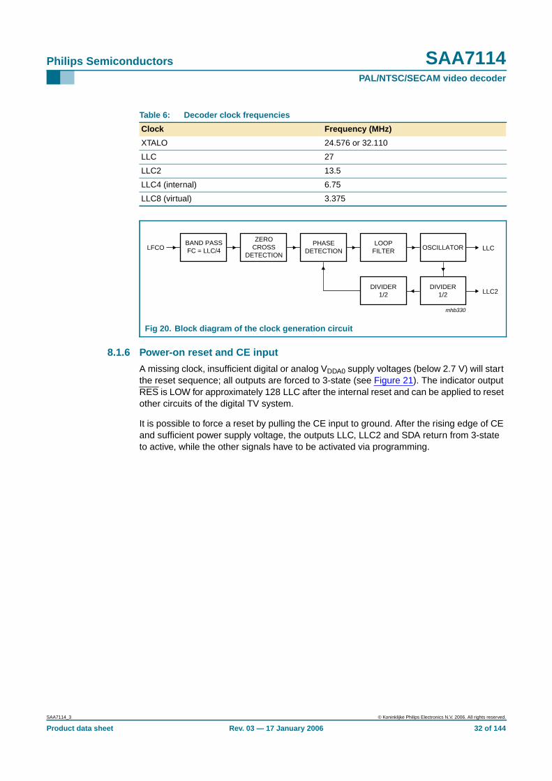
8.1.5 Clock generation circuit
The internal CGC generates all clock signals required for the video input processor.
The internal signal LFCO is a digital-to-analog converted signal provided by the horizontalPLL. It is the multiple of the line frequency:
• 6.75 MHz = 429 × fH (50 Hz), or
• 6.75 MHz = 432 × fH (60 Hz)
The LFCO signal is multiplied by a factor of 2 and 4 in the internal PLL circuit (includingphase detector, loop filtering, VCO and frequency divider) to obtain the output clocksignals. The rectangular output clocks have a 50 % duty factor.
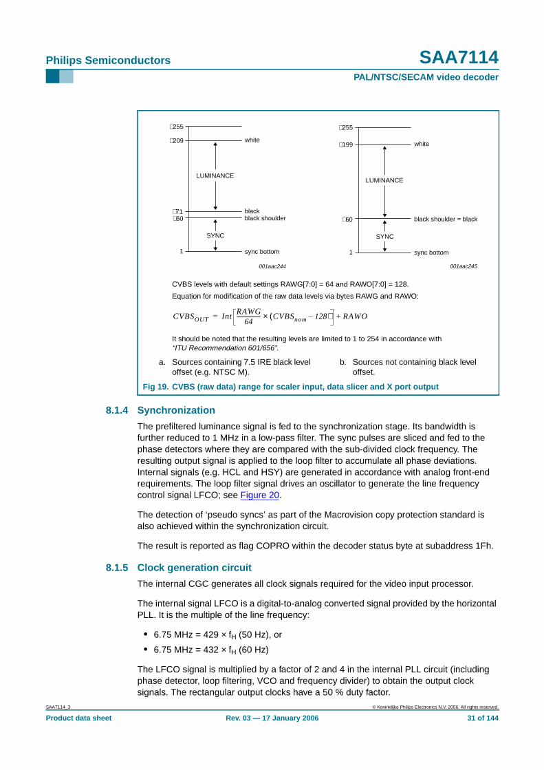
CVBS levels with default settings RAWG[7:0] = 64 and RAWO[7:0] = 128.
Equation for modification of the raw data levels via bytes RAWG and RAWO:
It should be noted that the resulting levels are limited to 1 to 254 in accordance with“ITU Recommendation 601/656”.
a. Sources containing 7.5 IRE black leveloffset (e.g. NTSC M).
b. Sources not containing black leveloffset.
Fig 19. CVBS (raw data) range for scaler input, data slicer and X port output
LUMINANCE
+255
+209
+71+60
1
white
sync bottom
black shoulderblack
SYNC
001aac244
LUMINANCE
+255
+199
+60
1
white
sync bottom
black shoulder = black
SYNC
001aac245
CVBSOUT IntRAWG
64----------------- CVBSnom 128–( )× RAWO+=
SAA7114_3 © Koninklijke Philips Electronics N.V. 2006. All rights reserved.
Product data sheet Rev. 03 — 17 January 2006 31 of 144
Philips Semiconductors SAA7114PAL/NTSC/SECAM video decoder
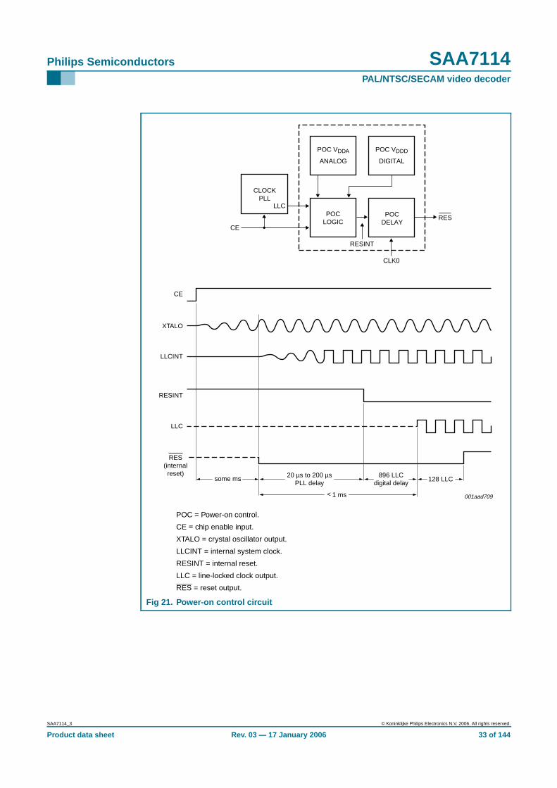
8.1.6 Power-on reset and CE input
A missing clock, insufficient digital or analog VDDA0 supply voltages (below 2.7 V) will startthe reset sequence; all outputs are forced to 3-state (see Figure 21). The indicator outputRES is LOW for approximately 128 LLC after the internal reset and can be applied to resetother circuits of the digital TV system.
It is possible to force a reset by pulling the CE input to ground. After the rising edge of CEand sufficient power supply voltage, the outputs LLC, LLC2 and SDA return from 3-stateto active, while the other signals have to be activated via programming.
Table 6: Decoder clock frequencies
Clock Frequency (MHz)
XTALO 24.576 or 32.110
LLC 27
LLC2 13.5
LLC4 (internal) 6.75
LLC8 (virtual) 3.375
Fig 20. Block diagram of the clock generation circuit
BAND PASSFC = LLC/4
ZEROCROSS
DETECTION
PHASEDETECTION
LOOPFILTER
DIVIDER1/2
DIVIDER1/2
OSCILLATOR
mhb330
LLC2
LLCLFCO
SAA7114_3 © Koninklijke Philips Electronics N.V. 2006. All rights reserved.
Product data sheet Rev. 03 — 17 January 2006 32 of 144
Philips Semiconductors SAA7114PAL/NTSC/SECAM video decoder
POC = Power-on control.
CE = chip enable input.
XTALO = crystal oscillator output.
LLCINT = internal system clock.
RESINT = internal reset.
LLC = line-locked clock output.
RES = reset output.
Fig 21. Power-on control circuit
001aad709
128 LLC896 LLC
digital delaysome ms 20 µs to 200 µs
PLL delay
< 1 ms
RES(internalreset)
LLC
RESINT
LLCINT
XTALO
CE
POC VDDA
POCLOGIC
ANALOG
POC VDDD
DIGITAL
POCDELAY
CLOCKPLL
CE
LLC
CLK0
RESINT
RES
SAA7114_3 © Koninklijke Philips Electronics N.V. 2006. All rights reserved.
Product data sheet Rev. 03 — 17 January 2006 33 of 144
Philips Semiconductors SAA7114PAL/NTSC/SECAM video decoder
8.2 Decoder output formatterThe output interface block of the decoder part contains the ITU 656 formatter for theexpansion port data output XPD7 to XPD0 (for a detailed description see Section 9.4.1)and the control circuit for the signals needed for the internal paths to the scaler and dataslicer part. It also controls the selection of the reference signals for the RT port (RTCO,RTS0 and RTS1) and the expansion port (XRH, XRV and XDQ).
The generation of the decoder data type control signals SET_RAW and SET VBI is alsodone within this block. These signals are decoded from the requested data type for thescaler input and/or the data slicer, selectable by the control registers LCR2 to LCR24 (seealso Section 10; subaddresses 41h to 57h).
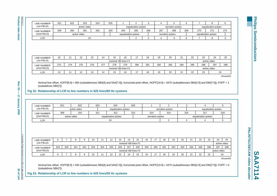
For each LCR value from 2 to 23 the data type can be programmed individually;LCR2 to LCR23 refer to line numbers. The selection in LCR24 values is valid for the restof the corresponding field. The upper nibble contains the value for field 1 (odd), the lowernibble for field 2 (even). The relationship between LCR values and line numbers can beadjusted via VOFF8 to VOFF0, located in subaddresses 5Bh (bit D4) and 5Ah(bits D7 to D0) and FOFF subaddress 5Bh (bit D7). The recommended values areVOFF[8:0] = 03h for 50 Hz sources (with FOFF = 0) and VOFF[8:0] = 06h for 60 Hzsources (with FOFF = 1), to accommodate line number conventions as used for PAL,SECAM and NTSC standards; see Figure 22 and Figure 23.
Table 7: Data formats at decoder output
Data type number Data type Decoder output data format
0 teletext EuroWST, CCST raw
1 European closed caption raw
2 Video Programming Service (VPS) raw
3 wide screen signalling bits raw
4 US teletext (WST) raw
5 US closed caption (line 21) raw
6 video component signal, VBI region Y-CB-CR 4 : 2 : 2
7 CVBS data raw
8 teletext raw
9 VITC/EBU time codes (Europe) raw
10 VITC/SMPTE time codes (USA) raw
11 reserved raw
12 US NABTS raw
13 MOJI (Japanese) raw
14 Japanese format switch (L20/22) raw
15 video component signal, active video region Y-CB-CR 4 : 2 : 2
SAA7114_3 © Koninklijke Philips Electronics N.V. 2006. All rights reserved.
Product data sheet Rev. 03 — 17 January 2006 34 of 144
xxxxxxxxxxxxxxxxxxxxx xxxxxxxxxxxxxxxxxxxxxxxxxx xxxxxxx x x x xxxxxxxxxxxxxxxxxxxxxxxxxxxxxx xxxxxxxxxxxxxxxxxxx xx xxxxxxx xxxxxxxxxxxxxxxxxxxxxxxxxxx xxxxxxxxxxxxxxxxxxx xxxxxx xxxxxxxxxxxxxxxxxxxxxxxxxxxxxxxxxxx xxxxxxxxxxxx x xxxxxxxxxxxxxxxxxxxxxx xxxxxxxxxxxxxxxxxxxxxxxxxxxxxx xxxxx xxxxxxxxxxxxxxxxxxxxxxxxxxxxxxxxxxxxxxxxxxxxxxxxxx xxxxxxxxxxxxxxxxxxxxxxxxxxxxxxxxx xxxxxxxxxxxxxxxxxxxx xxx
SA
A7114_3
Product data shee
Philips S
emiconductors
SA
A7114
PAL/N
TS
C/S
EC
AM
video decoder
esses 5Bh[2:0] and 59h[7:0]); FOFF = 1
521 522
active video
active video
equalization pulses
equalization pulses
equalization pulses
equalization pulses
serration pulses
serration pulses
523 524 525 1 2 3 4 5 6 7 8 9
259 260 261
6 7 8 9
262 263 264 265 266 267 268 269 270 271 272
LINE NUMBER(1st FIELD)
LINE NUMBER(2nd FIELD)
001aad425
active video
active video
22 23 24 25
285 286 287 288
22 23 24
esses 5Bh[2:0] and 59h[7:0]); FOFF = 0
equalization pulses
equalization pulses
3 4 5
316 317 318
3 4 5
001aad426
active video
active video
0 21 22 23 24 25
3 334 335 336 337 338
0 21 22 23 24
© K
oninklijke Philips E
lectronics N.V. 2006. A
ll rights reserved.
tR
ev. 03 — 17 January 2006
35 of 144
Vertical line offset, VOFF[8:0] = 06h (subaddresses 5Bh[4] and 5Ah[7:0]); horizontal pixel offset, HOFF[10:0] = 347h (subaddr(subaddress 5Bh[7])
Fig 22. Relationship of LCR to line numbers in 525 lines/60 Hz systems
24 2 3 4 5LCR
10 11
nominal VBI lines F1
nominal VBI lines F2
12 13 14 15 16 17 18 19 20 21LINE NUMBER(1st FIELD)
LINE NUMBER(2nd FIELD)
LCR
273 274 275 276 277 278 279 280 281 282 283 284
10 11 12 13 14 15 16 17 18 19 20 21
Vertical line offset, VOFF[8:0] = 03h (subaddresses 5Bh[4] and 5Ah[7:0]); horizontal pixel offset, HOFF[10:0] = 347h (subaddr(subaddress 5Bh[7])
Fig 23. Relationship of LCR to line numbers in 625 lines/50 Hz systems
621 622
active video
active video
equalization pulses
equalization pulses
serration pulses
serration pulses
623 624 625 1 2LINE NUMBER(1st FIELD)
LINE NUMBER(2nd FIELD)
LCR
309 310 311 312 313 314 315
224
6 7
nominal VBI lines F1
nominal VBI lines F2
8 9 10 11 12 13 14 15 16 17 18 19 2LINE NUMBER(1st FIELD)
LINE NUMBER(2nd FIELD)
LCR
319 320 321 322 323 324 325 326 327 328 329 330 331 332 33
6 7 8 9 10 11 12 13 14 15 16 17 18 19 2
Philips Semiconductors SAA7114PAL/NTSC/SECAM video decoder
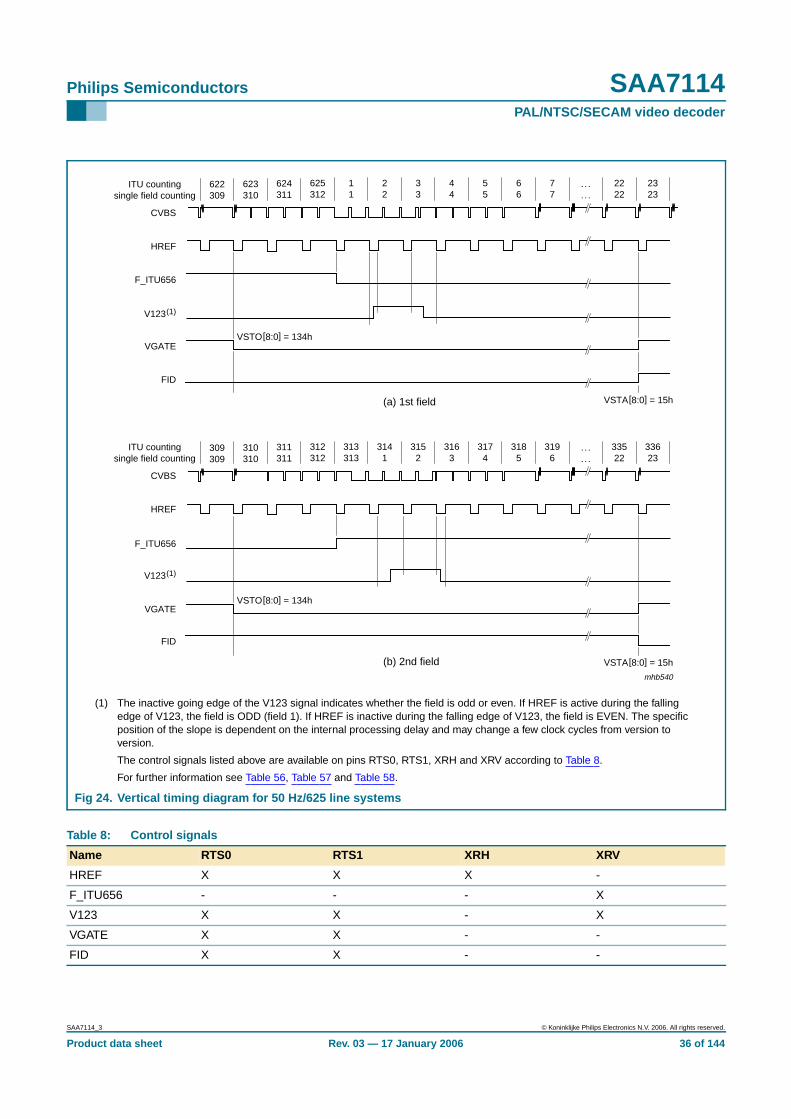
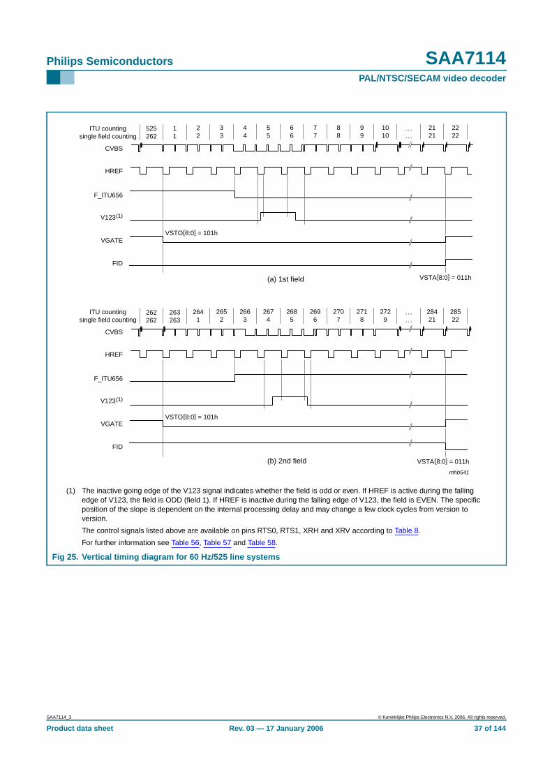
(1) The inactive going edge of the V123 signal indicates whether the field is odd or even. If HREF is active during the fallingedge of V123, the field is ODD (field 1). If HREF is inactive during the falling edge of V123, the field is EVEN. The specificposition of the slope is dependent on the internal processing delay and may change a few clock cycles from version toversion.
The control signals listed above are available on pins RTS0, RTS1, XRH and XRV according to Table 8.
For further information see Table 56, Table 57 and Table 58.
Fig 24. Vertical timing diagram for 50 Hz/625 line systems
mhb540
VGATEVSTO[8:0] = 134h
VSTA[8:0] = 15h(a) 1st field
CVBS
ITU countingsingle field counting
11
22
33
44
55
66
77
.. .
. . .2222
625312
624311
623310
622309
2323
FID
HREF
F_ITU656
V123(1)
VGATE
CVBS
ITU countingsingle field counting
FID
HREF
F_ITU656
V123(1)
VSTO[8:0] = 134h
VSTA[8:0] = 15h(b) 2nd field
313313
3141
3152
3163
3174
3185
3196
.. .
. . .33522
312312
311311
310310
309309
33623
Table 8: Control signals
Name RTS0 RTS1 XRH XRV
HREF X X X -
F_ITU656 - - - X
V123 X X - X
VGATE X X - -
FID X X - -
SAA7114_3 © Koninklijke Philips Electronics N.V. 2006. All rights reserved.
Product data sheet Rev. 03 — 17 January 2006 36 of 144
Philips Semiconductors SAA7114PAL/NTSC/SECAM video decoder
(1) The inactive going edge of the V123 signal indicates whether the field is odd or even. If HREF is active during the fallingedge of V123, the field is ODD (field 1). If HREF is inactive during the falling edge of V123, the field is EVEN. The specificposition of the slope is dependent on the internal processing delay and may change a few clock cycles from version toversion.
The control signals listed above are available on pins RTS0, RTS1, XRH and XRV according to Table 8.
For further information see Table 56, Table 57 and Table 58.
Fig 25. Vertical timing diagram for 60 Hz/525 line systems
mhb541
VGATEVSTO[8:0] = 101h
VSTA[8:0] = 011h(a) 1st field
CVBS
ITU countingsingle field counting
44
55
66
77
88
99
1010
.. .
. . .2121
33
22
11
525262
2222
FID
HREF
F_ITU656
V123(1)
VGATE
CVBS
ITU countingsingle field counting
FID
HREF
F_ITU656
V123(1)
VSTO[8:0] = 101h
VSTA[8:0] = 011h(b) 2nd field
2663
2674
2685
2696
2707
2718
2729
.. .
. . .28421
2652
2641
263263
262262
28522
SAA7114_3 © Koninklijke Philips Electronics N.V. 2006. All rights reserved.
Product data sheet Rev. 03 — 17 January 2006 37 of 144
Philips Semiconductors SAA7114PAL/NTSC/SECAM video decoder
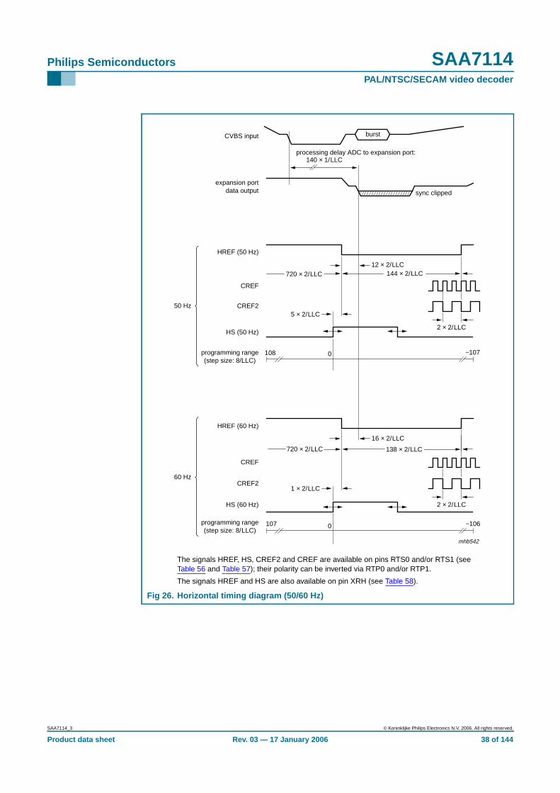
The signals HREF, HS, CREF2 and CREF are available on pins RTS0 and/or RTS1 (seeTable 56 and Table 57); their polarity can be inverted via RTP0 and/or RTP1.
The signals HREF and HS are also available on pin XRH (see Table 58).
Fig 26. Horizontal timing diagram (50/60 Hz)
108 −107
107 −106
mhb542
CVBS input
140 × 1/LLC
5 × 2/LLC
expansion portdata output
12 × 2/LLC720 × 2/LLC 144 × 2/LLC
138 × 2/LLC720 × 2/LLC
burst
processing delay ADC to expansion port:
0
0
2 × 2/LLC
2 × 2/LLC
HREF (60 Hz)
HS (60 Hz)
sync clipped
16 × 2/LLC
1 × 2/LLC
programming range(step size: 8/LLC)
programming range(step size: 8/LLC)
HS (50 Hz)
HREF (50 Hz)
CREF
CREF250 Hz
CREF
CREF260 Hz
SAA7114_3 © Koninklijke Philips Electronics N.V. 2006. All rights reserved.
Product data sheet Rev. 03 — 17 January 2006 38 of 144
Philips Semiconductors SAA7114PAL/NTSC/SECAM video decoder
8.3 ScalerThe High Performance video Scaler (HPS) is based on the system as implemented inprevious products (e.g. SAA7140), but with some aspects enhanced. Vertical upsamplingis supported and the processing pipeline buffer capacity is enhanced, to allow moreflexible video stream timing at the image port, discontinuous transfers, and handshake.The internal data flow from block to block is discontinuous dynamically, due to the scalingprocess.
The flow is controlled by internal data valid and data request flags (internal handshakesignalling) between the sub-blocks; therefore the entire scaler acts as a pipeline buffer.Depending on the actual programmed scaling parameters the effective buffer can exceedto an entire line. The access/bandwidth requirements to the VGA frame buffer are reducedsignificantly.
The high performance video scaler in the SAA7114 has the following major blocks:
• Acquisition control (horizontal and vertical timer) and task handling (theregion/field/frame based processing)
• Prescaler, for horizontal downscaling by an integer factor, combined with appropriateband limiting filters, especially anti-aliasing for CIF format
• Brightness, saturation, contrast control for scaled output data
• Line buffer, with asynchronous read and write, to support vertical upscaling (e.g. forvideophone application, converting 240 into 288 lines, Y-CB-CR 4 : 2 : 2)
• Vertical scaling, with phase accurate Linear Phase Interpolation (LPI) for zoom anddownscale, or phase accurate Accumulation Mode (ACM) for large downscaling ratiosand better alias suppression
• Variable Phase Delay (VPD), operates as horizontal phase accurate interpolation forarbitrary non-integer scaling ratios, supporting conversion between square andrectangular pixel sampling
• Output formatter for scaled Y-CB-CR 4 : 2 : 2, Y-CB-CR 4 : 1 : 1 and Yonly (format alsoused for raw data)
• FIFO, 32-bit wide, with 64 pixel capacity in Y-CB-CR formats
• Output interface, 8-bit or 16-bit (only if extended by H port) data pins wide,synchronous or asynchronous operation, with stream events on discrete pins, orcoded in the data stream
The overall H and V zooming (HV_zoom) is restricted by the input/output data raterelationships. With a safety margin of 2 % for running in and running out, the maximum
HV_zoom is equal to:
For example:
1. Input from decoder: 50 Hz, 720 pixel, 288 lines, 16-bit data at 13.5 MHz data rate,1 cycle per pixel; output: 8-bit data at 27 MHz, 2 cycles per pixel; the maximum
HV_zoom is equal to:
0.98T_input_field T_v_blanking–
in_pixel in_lines× out_cycle_per_pix× T_out_clk×------------------------------------------------------------------------------------------------------------------------------×
0.9820 ms 24 64 µs×–
720 288× 2× 37 ns×----------------------------------------------------- 1.18=×
SAA7114_3 © Koninklijke Philips Electronics N.V. 2006. All rights reserved.
Product data sheet Rev. 03 — 17 January 2006 39 of 144
Philips Semiconductors SAA7114PAL/NTSC/SECAM video decoder
2. Input from X port: 60 Hz, 720 pixel, 240 lines, 8-bit data at 27 MHz data rate(ITU 656), 2 cycles per pixel; output via I + H port: 16-bit data at 27 MHz clock,1 cycle per pixel; the maximum HV_zoom is equal to:
The video scaler receives its input signal from the video decoder or from the expansionport (X port). It gets 16-bit Y-CB-CR 4 : 2 : 2 input data at a continuous rate of 13.5 MHzfrom the decoder. Discontinuous data stream can be accepted from the expansion port(X port), normally 8-bit wide ITU 656 such as Y-CB-CR data, accompanied by a pixelqualifier on XDQ.
The input data stream is sorted into two data paths, one for luminance (or raw samples)and one for time-multiplexed chrominance CB and CR samples. An Y-CB-CR 4 : 1 : 1 inputformat is converted to 4 : 2 : 2 for the horizontal prescaling and vertical filter scalingoperation.
The scaler operation is defined by two programming pages A and B, representing twodifferent tasks, that can be applied field alternating or to define two regions in a field (e.g.with different scaling range, factors and signal source during odd and even fields).
Each programming page contains control:
• For signal source selection and formats
• For task handling and trigger conditions
• For input and output acquisition window definition
• For H-prescaler, V-scaler and H-phase scaling
Raw VBI data is handled as a specific input format and needs its own programming page(equals own task).
In VBI pass through operation the processing of prescaler and vertical scaling has to beset to no-processing, however, the horizontal fine scaling VPD can be activated.Upscaling (oversampling, zooming), free of frequency folding, up to a factor of 3.5 can beachieved, as required by some software data slicing algorithms.
These raw samples are transported through the image port as valid data and can beoutput as Yonly format. The lines are framed by SAV and EAV codes.
8.3.1 Acquisition control and task handling (subaddresses 80h, 90h, 91h,94h to 9Fh and C4h to CFh)
The acquisition control receives horizontal and vertical synchronization signals from thedecoder section or from the X port. The acquisition window is generated via pixel and linecounters at the appropriate places in the data path. From X port only qualified pixels andlines (lines with qualified pixel) are counted.
The acquisition window parameters are as follows:
• Signal source selection regarding input video stream and formats from the decoder, orfrom X port (programming bits SCSRC[1:0] 91h[5:4] and FSC[2:0] 91h[2:0])
Remark : The input of raw VBI data from the internal decoder should be controlled viathe decoder output formatter and the LCR registers; see Section 8.2
0.9816.666ms 22 64 µs×–720 240× 1× 37 ns×---------------------------------------------------------- 2.34=×
SAA7114_3 © Koninklijke Philips Electronics N.V. 2006. All rights reserved.
Product data sheet Rev. 03 — 17 January 2006 40 of 144
Philips Semiconductors SAA7114PAL/NTSC/SECAM video decoder
• Vertical offset defined in lines of the video source, parameter YO[11:0] 99h[3:0]98h[7:0]
• Vertical length defined in lines of the video source, parameter YS[11:0] 9Bh[3:0]9Ah[7:0]
• Vertical length defined in number of target lines, as a result of vertical scaling,parameter YD[11:0] 9Fh[3:0] 9Eh[7:0]
• Horizontal offset defined in number of pixels of the video source, parameter XO[11:0]95h[3:0] 94h[7:0]
• Horizontal length defined in number of pixels of the video source, parameter XS[11:0]97h[3:0] 96h[7:0]
• Horizontal destination size, defined in target pixels after fine scaling, parameterXD[11:0] 9Dh[3:0] 9Ch[7:0]
The source start offset (XO11 to XO0 and YO11 to YO0) opens the acquisition window,and the target size (XD11 to XD0 and YD11 to YD0) closes the window, however thewindow is cut vertically if there are less output lines than expected. The trigger events forthe pixel and line counts are the horizontal and vertical reference edges as defined insubaddress 92h. The task handling is controlled by subaddress 90h; see Section 8.3.1.2.
8.3.1.1 Input field processing
The trigger event for the field sequence detection from external signals (X port) aredefined in subaddress 92h. From the X port the state of the scalers H reference signal atthe time of the V reference edge is taken as field sequence identifier FID. For example, ifthe falling edge of the XRV input signal is the reference and the state of XRH input islogic 0 at that time, the detected field ID is logic 0.
The bits XFDV[92h[7]] and XFDH[92h[6]] define the detection event and state of the flagfrom the X port. For the default setting of XFDV and XFDH at ‘00’ the state of the H-inputat the falling edge of the V-input is taken.
The scaler directly gets a corresponding field ID information from the SAA7114 decoderpath.
The FID flag is used to determine whether the first or second field of a frame is going to beprocessed within the scaler and it is used as trigger condition for the task handling (seebits STRC[1:0] 90h[1:0]).
According to ITU 656, when FID is at logic 0 means first field of a frame. To ease theapplication, the polarities of the detection results on the X port signals and the internaldecoder ID can be changed via XFDH.
As the V-sync from the decoder path has a half line timing (due to the interlaced videosignal), but the scaler processing only knows about full lines, during 1st fields from thedecoder the line count of the scaler possibly shifts by one line, compared to the 2nd field.This can be compensated for by switching the V-trigger event, as defined by XDV0, to theopposite V-sync edge or by using the vertical scalers phase offsets. The vertical timing ofthe decoder can be seen in Figure 24 and Figure 25.
As the H and V reference events inside the ITU 656 data stream (from X port) and thereal-time reference signals from the decoder path are processed differently, the triggerevents for the input acquisition also have to be programmed differently.
SAA7114_3 © Koninklijke Philips Electronics N.V. 2006. All rights reserved.
Product data sheet Rev. 03 — 17 January 2006 41 of 144
Philips Semiconductors SAA7114PAL/NTSC/SECAM video decoder
8.3.1.2 Task handling
The task handler controls the switching between the two programming register sets. It iscontrolled by subaddresses 90h and C0h. A task is enabled via the global control bitsTEA[80h[4]] and TEB[80h[5]].
The handler is then triggered by events, which can be defined for each register set.
In the event of a programming error the task handling and the complete scaler can bereset to the initial states by setting the software reset bit SWRST[88h[5]] to logic 0.Especially if the programming registers, related acquisition window and scale arereprogrammed while a task is active, a software reset must be performed afterprogramming.
Contrary to the disabling/enabling of a task, which is evaluated at the end of a runningtask, when SWRST is at logic 0 it sets the internal state machines directly to their idlestates.
The start condition for the handler is defined by bits STRC[1:0] 90h[1:0] and means: startimmediately, wait for next V-sync, next FID at logic 0 or next FID at logic 1. The FID isevaluated, if the vertical and horizontal offsets are reached.
When RPTSK[90h[2]] is at logic 1 the actual running task is repeated (under the definedtrigger conditions), before handing control over to the alternate task.
To support field rate reduction, the handler is also enabled to skip fields (bits FSKP[2:0]90h[5:3]) before executing the task. A TOGGLE flag is generated (used for the correctoutput field processing), which changes state at the beginning of a task, every time a taskis activated; examples are given in Section 8.3.1.3.
Remarks:
• To activate a task the start condition must be fulfilled and the acquisitionwindow offsets must be reached.
For example, in case of ‘start immediately’, and two regions are defined for one field,the offset of the lower region must be greater than (offset + length) of the upperregion, if not, the actual counted H and V position at the end of the upper task isbeyond the programmed offsets and the processing will ‘wait for next V’.
Table 9: Processing trigger and start
XDV192h[5]
XDV092h[4]
XDH92h[2]
Description
Internal decoder: The processing triggers at the falling edge of theV123 pulse [see Figure 24 (50 Hz) and Figure 25 (60 Hz)], and startsearliest with the rising edge of the decoder HREF at line number:
0 1 0 4/7 (50/60 Hz, 1st field), respectively 3/6 (50/60 Hz, 2nd field)(decoder count)
0 0 0 2/5 (50/60 Hz, 1st field), respectively 2/5 (50/60 Hz, 2nd field)(decoder count)
0 0 0 External ITU 656 stream: The processing starts earliest with SAV atline number 23 (50 Hz system), respectively line 20 (60 Hz system)(according to ITU 656 count)
SAA7114_3 © Koninklijke Philips Electronics N.V. 2006. All rights reserved.
Product data sheet Rev. 03 — 17 January 2006 42 of 144
Philips Semiconductors SAA7114PAL/NTSC/SECAM video decoder
• Basically the trigger conditions are checked, when a task is activated. It isimportant to realize, that they are not checked while a task is inactive. So you can nottrigger to next logic 0 or logic 1 with overlapping offset and active video rangesbetween the tasks (e.g. task A STRC[1:0] = 2, YO[11:0] = 310 and task BSTRC[1:0] = 3, YO[11:0] = 310 results in output field rate of 50⁄3 Hz).
• After power-on or software reset (via SWRST[88h[5]]) task B gets priority overtask A
8.3.1.3 Output field processing
As a reference for the output field processing, two signals are available for the back-endhardware.
These signals are the input field ID from the scaler source and a TOGGLE flag, whichshows that an active task is used an odd (1, 3, 5...) or even (2, 4, 6...) number of times.Using a single or both tasks and reducing the field or frame rate with the task handlingfunction, the TOGGLE information can be used to reconstruct an interlaced scaled pictureat a reduced frame rate. The TOGGLE flag isn’t synchronized to the input field detection,as it is only dependent on the interpretation of this information by the external hardware,whether the output of the scaler is processed correctly; see Section 8.3.3.
With OFIDC = 0, the scalers input field ID is available as output field ID on bit D6 of SAVand EAV, respectively on pin IGP0 (IGP1), if FID output is selected.
When OFIDC[90h[6]] = 1, the TOGGLE information is available as output field ID on bit D6of SAV and EAV, respectively on pin IGP0 (IGP1), if FID output is selected.
Additionally the bit D7 of SAV and EAV can be defined via CONLH[90h[7]].CONLH[90h[7]] = 0 (default) sets D7 to logic 1, a logic 1 inverts the SAV/EAV bit D7. So itis possible to mark the output of both tasks by different SAV/EAV codes. This bit can alsobe seen as ‘task flag’ on pins IGP0 (IGP1), if TASK output is selected.
SAA7114_3 © Koninklijke Philips Electronics N.V. 2006. All rights reserved.
Product data sheet Rev. 03 — 17 January 2006 43 of 144
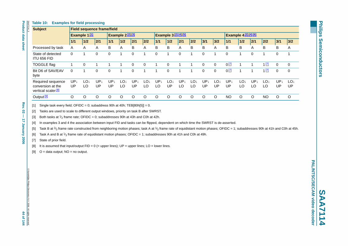
xxxxxxxxxxxxxxxxxxxxx xxxxxxxxxxxxxxxxxxxxxxxxxx xxxxxxx x x x xxxxxxxxxxxxxxxxxxxxxxxxxxxxxx xxxxxxxxxxxxxxxxxxx xx xxxxxxx xxxxxxxxxxxxxxxxxxxxxxxxxxx xxxxxxxxxxxxxxxxxxx xxxxxx xxxxxxxxxxxxxxxxxxxxxxxxxxxxxxxxxxx xxxxxxxxxxxx x xxxxxxxxxxxxxxxxxxxxxx xxxxxxxxxxxxxxxxxxxxxxxxxxxxxx xxxxx xxxxxxxxxxxxxxxxxxxxxxxxxxxxxxxxxxxxxxxxxxxxxxxxxx xxxxxxxxxxxxxxxxxxxxxxxxxxxxxxxxx xxxxxxxxxxxxxxxxxxxx xxx
SA
A7114_3
Product data shee
Philips S
emiconductors
SA
A7114
PAL/N
TS
C/S
EC
AM
video decoder
rted.
= 1; subaddresses 90h at 41h and C0h at 45h.
Table 10: Examples for field processing
Subject Field sequence frame/field
Example 1 [1] Example 2 [2] [3] Example 3 [2] [4] [5] Example 4 [2] [4] [6]
1/1 1/2 2/1 1/1 1/2 2/1 2/2 1/1 1/2 2/1 2/2 3/1 3/2 1/1 1/2 2/1 2/2 3/1 3/2
B A B B A
1 0 1 0 1
7] 1 1 1 [7] 0 07] 1 1 1 [7] 0 0
↓ LO↓LO
UP↓LO
LO↓LO
UP↓UP
LO↓UP
O O NO O O
© K
oninklijke Philips E
lectronics N.V. 2006. A
ll rights reserved.
tR
ev. 03 — 17 January 2006
44 of 144
[1] Single task every field; OFIDC = 0; subaddress 90h at 40h; TEB[80h[5]] = 0.
[2] Tasks are used to scale to different output windows, priority on task B after SWRST.
[3] Both tasks at 1⁄2 frame rate; OFIDC = 0; subaddresses 90h at 43h and C0h at 42h.
[4] In examples 3 and 4 the association between input FID and tasks can be flipped, dependent on which time the SWRST is de-asse
[5] Task B at 2⁄3 frame rate constructed from neighboring motion phases; task A at 1⁄3 frame rate of equidistant motion phases; OFIDC
[6] Task A and B at 1⁄3 frame rate of equidistant motion phases; OFIDC = 1; subaddresses 90h at 41h and C0h at 49h.
[7] State of prior field.
[8] It is assumed that input/output FID = 0 (= upper lines); UP = upper lines; LO = lower lines.
[9] O = data output; NO = no output.
Processed by task A A A B A B A B B A B B A B
State of detectedITU 656 FID
0 1 0 0 1 0 1 0 1 0 1 0 1 0
TOGGLE flag 1 0 1 1 1 0 0 1 0 1 1 0 0 0 [
Bit D6 of SAV/EAVbyte
0 1 0 0 1 0 1 1 0 1 1 0 0 0 [
Required sequenceconversion at thevertical scaler [8]
UP↓UP
LO↓LO
UP↓UP
UP↓UP
LO↓LO
UP↓UP
LO↓LO
UP↓LO
LO↓UP
UP↓LO
LO↓LO
UP↓UP
LO↓UP
UPUP
Output [9] O O O O O O O O O O O O O NO
Philips Semiconductors SAA7114PAL/NTSC/SECAM video decoder
8.3.2 Horizontal scaling
The overall horizontal required scaling factor has to be split into a binary and a rationalvalue according to the equation:
where the parameter of prescaler XPSC[5:0] = 1 to 63 and the parameter of VPD phaseinterpolation XSCY[12:0] = 300 to 8191 (0 to 299 are only theoretical values). Forexample, 1⁄3.5 is to split in 1⁄4 × 1.14286. The binary factor is processed by the prescaler,the arbitrary non-integer ratio is achieved via the variable phase delay VPD circuitry,called horizontal fine scaling. The latter calculates horizontally interpolated new sampleswith a 6-bit phase accuracy, which relates to less than 1 ns jitter for regular samplingscheme. Prescaler and fine scaler create the horizontal scaler of the SAA7114.
Using the accumulation length function of the prescaler (XACL[5:0] A1h[5:0]), applicationand destination dependent (e.g. scale for display or for a compression machine), acompromise between visible bandwidth and alias suppression can be determined.
8.3.2.1 Horizontal prescaler (subaddresses A0h to A7h and D0h to D7h)
The prescaling function consists of an FIR anti-alias filter stage and an integer prescaler,which creates an adaptive prescale dependent low-pass filter to balance sharpness andaliasing effects.
The FIR prefilter stage implements different low-pass characteristics to reduce alias fordownscales in the range of 1 to 1⁄2. A CIF optimized filter is built-in, which reducesartefacts for CIF output formats (to be used in combination with the prescaler set to1⁄2 scale); see Table 11.
The function of the prescaler is defined by:
• An integer prescaling ratio XPSC[5:0] A0h[5:0] (equals 1 to 63), which covers theinteger downscale range 1 to 1⁄63
• An averaging sequence length XACL[5:0] A1h[5:0] (equals 0 to 63); range 1 to 64
• A DC gain renormalization XDCG[2:0] A2h[2:0]; 1 down to 1⁄128
• The bit XC2_1[A2h[3]], which defines the weighting of the incoming pixels during theaveraging process:
– XC2_1 = 0 ⇒ 1 + 1...+ 1 + 1
– XC2_1 = 1 ⇒ 1 + 2...+ 2 + 1
The prescaler creates a prescale dependent FIR low-pass, with up to (64 + 7) filter taps.The parameter XACL[5:0] can be used to vary the low-pass characteristic for a giveninteger prescale of 1⁄XPSC[5:0]. The user can therefore decide between signal bandwidth(sharpness impression) and alias.
Equation for XPSC[5:0] calculation is:
H-scale ratio output pixelinput pixel----------------------------=
H-scale ratio1
XPSC[5:0]--------------------------
1024XSCY[12:0]------------------------------×=
XPSC[5:0] lower integer ofNpix_inNpix_out----------------------=
SAA7114_3 © Koninklijke Philips Electronics N.V. 2006. All rights reserved.
Product data sheet Rev. 03 — 17 January 2006 45 of 144
Philips Semiconductors SAA7114PAL/NTSC/SECAM video decoder
Where:
• The range is 1 to 63 (value 0 is not allowed )
• Npix_in = number of input pixel, and
• Npix_out = number of desired output pixel over the complete horizontal scaler
The use of the prescaler results in a XACL[5:0] and XC2_1 dependent gainamplification. The amplification can be calculated according to the equation:
DC gain = (XC2_1 + 1) × XACL[5:0] + (1 − XC2_1)
It is recommended to use sequence lengths and weights, which results in a 2N DC gain
amplification, as these amplitudes can be renormalized by the XDCG[2:0] controlled
shifter of the prescaler.
The renormalization range of XDCG[2:0] is 1, 1⁄2 down to 1⁄128.
Other amplifications have to be normalized by using the following BCS control circuitry. Inthese cases the prescaler has to be set to an overall gain of ≤ 1, e.g. for an accumulationsequence of ‘1 + 1 + 1’ (XACL[5:0] = 2 and XC2_1 = 0), XDCG[2:0] must be set to ‘010’,this equals 1⁄4 and the BCS has to amplify the signal to 4⁄3 (SATN[7:0] and CONT[7:0]value = lower integer of 4⁄3 × 64).
The use of XACL[5:0] is XPSC[5:0] dependent. XACL[5:0] must be < 2 × XPSC[5:0].
XACL[5:0] can be used to find a compromise between bandwidth (sharpness) and aliaseffects.
Remark : Due to bandwidth considerations XPSC[5:0] and XACL[5:0] can be chosendifferently to the previously mentioned equations or Table 12, as the H-phase scaling isable to scale in the range from zooming up by factor 3 to downscaling by a factor of1024⁄8191.
Figure 29 and Figure 30 show some resulting frequency characteristics of the prescaler.
Table 12 shows the recommended prescaler programming. Other programming, otherthan given in Table 12, may result in better alias suppression, but the resulting DC gainamplification needs to be compensated by the BCS control, according to the equation:
Where:
• 2XDCG[2:0] ≥ DC gain
• DC gain = (XC2_1 + 1) × XACL[5:0] + (1 − XC2_1)
For example, if XACL[5:0] = 5, XC2_1 = 1, then the DC gain = 10 and the requiredXDCG[2:0] = 4.
The horizontal source acquisition timing and the prescaling ratio is identical for both theluminance path and chrominance path, but the FIR filter settings can be defined differentlyin the two channels.
1
2N
------
CONT[7:0] SATN[7:0] lower integer of2
XDCG[2:0]
DC gain 64×--------------------------------= =
SAA7114_3 © Koninklijke Philips Electronics N.V. 2006. All rights reserved.
Product data sheet Rev. 03 — 17 January 2006 46 of 144
Philips Semiconductors SAA7114PAL/NTSC/SECAM video decoder
Fade-in and fade-out of the filters is achieved by copying an original source sample eachas first and last pixel after prescaling.
Figure 27 and Figure 28 show the frequency characteristics of the selectable FIR filters.
Table 11: FIR prefilter functions
PFUV[1:0] A2h[7:6] andPFY[1:0] A2h[5:4]
Luminance filter coefficients Chrominance coefficients
00 bypassed bypassed
01 1 2 1 1 2 1
10 −1 1 1.75 4.5 1.75 1 −1 3 8 10 8 3
11 1 2 2 2 1 1 2 2 2 1
Fig 27. Luminance prefilter characteristic
Fig 28. Chrominance prefilter characteristic
mhb543
f_sig/f_clock0 0.50.40.2 0.30.1 0.450.350.15 0.250.05
−18−21−24−27
−30−33−36−39
−6−9
−12−15
630
−3
V(dB)
−42
(3)
(2)
(1)
(1) PFY[1:0] = 01.(2) PFY[1:0] = 10.(3) PFY[1:0] = 11.
mhb544
(3)
(2)
(1)
(1) PFUV[1:0] = 01.(2) PFUV[1:0] = 10.(3) PFUV[1:0] = 11.
f_sig/f_clock0 0.250.200.10 0.150.05 0.2250.1750.075 0.1250.025
−18−21−24−27
−30−33−36−39
−6−9
−12−15
630
−3
V(dB)
−42
SAA7114_3 © Koninklijke Philips Electronics N.V. 2006. All rights reserved.
Product data sheet Rev. 03 — 17 January 2006 47 of 144
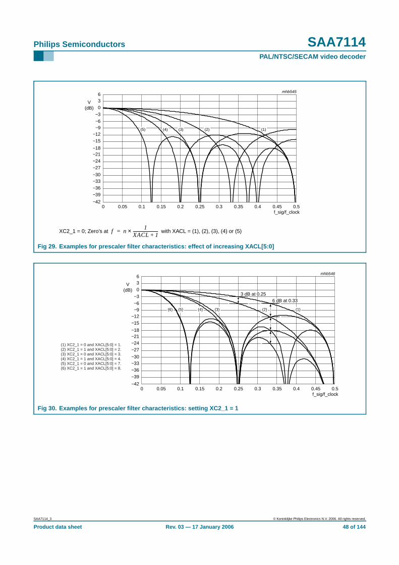
Philips Semiconductors SAA7114PAL/NTSC/SECAM video decoder
XC2_1 = 0; Zero’s at with XACL = (1), (2), (3), (4) or (5)
Fig 29. Examples for prescaler filter characteristics: effect of increasing XACL[5:0]
mhb545
(3)(4)(5) (2) (1)
f_sig/f_clock0 0.50.40.2 0.30.1 0.450.350.15 0.250.05
−18−21−24−27
−30−33−36−39
−6−9
−12−15
630
−3
V(dB)
−42
f n1
XACL 1+-------------------------×=
Fig 30. Examples for prescaler filter characteristics: setting XC2_1 = 1
mhb546
(3)(4)(5)(6) (2) (1)
3 dB at 0.256 dB at 0.33
(1) XC2_1 = 0 and XACL[5:0] = 1.(2) XC2_1 = 1 and XACL[5:0] = 2.(3) XC2_1 = 0 and XACL[5:0] = 3.(4) XC2_1 = 1 and XACL[5:0] = 4.(5) XC2_1 = 0 and XACL[5:0] = 7.(6) XC2_1 = 1 and XACL[5:0] = 8.
f_sig/f_clock0 0.50.40.2 0.30.1 0.450.350.15 0.250.05
−18−21−24−27
−30−33−36−39
−6−9
−12−15
630
−3
V(dB)
−42
SAA7114_3 © Koninklijke Philips Electronics N.V. 2006. All rights reserved.
Product data sheet Rev. 03 — 17 January 2006 48 of 144
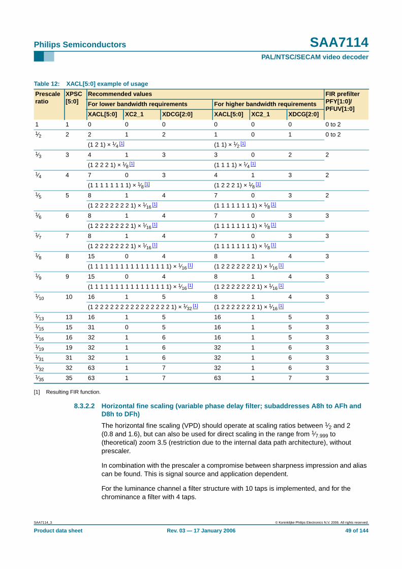
Philips Semiconductors SAA7114PAL/NTSC/SECAM video decoder
[1] Resulting FIR function.
8.3.2.2 Horizontal fine scaling (variable phase delay filter; subaddresses A8h to AFh andD8h to DFh)
The horizontal fine scaling (VPD) should operate at scaling ratios between 1⁄2 and 2(0.8 and 1.6), but can also be used for direct scaling in the range from 1⁄7.999 to(theoretical) zoom 3.5 (restriction due to the internal data path architecture), withoutprescaler.
In combination with the prescaler a compromise between sharpness impression and aliascan be found. This is signal source and application dependent.
For the luminance channel a filter structure with 10 taps is implemented, and for thechrominance a filter with 4 taps.
Table 12: XACL[5:0] example of usage
Prescaleratio
XPSC[5:0]
Recommended values FIR prefilterPFY[1:0]/PFUV[1:0]
For lower bandwidth requirements For higher bandwidth requirements
XACL[5:0] XC2_1 XDCG[2:0] XACL[5:0] XC2_1 XDCG[2:0]
1 1 0 0 0 0 0 0 0 to 21⁄2 2 2 1 2 1 0 1 0 to 2
(1 2 1) × 1⁄4 [1] (1 1) × 1⁄2 [1]
1⁄3 3 4 1 3 3 0 2 2
(1 2 2 2 1) × 1⁄8 [1] (1 1 1 1) × 1⁄4 [1]
1⁄4 4 7 0 3 4 1 3 2
(1 1 1 1 1 1 1 1) × 1⁄8 [1] (1 2 2 2 1) × 1⁄8 [1]
1⁄5 5 8 1 4 7 0 3 2
(1 2 2 2 2 2 2 2 1) × 1⁄16[1] (1 1 1 1 1 1 1 1) × 1⁄8 [1]
1⁄6 6 8 1 4 7 0 3 3
(1 2 2 2 2 2 2 2 1) × 1⁄16[1] (1 1 1 1 1 1 1 1) × 1⁄8 [1]
1⁄7 7 8 1 4 7 0 3 3
(1 2 2 2 2 2 2 2 1) × 1⁄16[1] (1 1 1 1 1 1 1 1) × 1⁄8 [1]
1⁄8 8 15 0 4 8 1 4 3
(1 1 1 1 1 1 1 1 1 1 1 1 1 1 1 1) × 1⁄16[1] (1 2 2 2 2 2 2 2 1) × 1⁄16
[1]
1⁄9 9 15 0 4 8 1 4 3
(1 1 1 1 1 1 1 1 1 1 1 1 1 1 1 1) × 1⁄16[1] (1 2 2 2 2 2 2 2 1) × 1⁄16
[1]
1⁄10 10 16 1 5 8 1 4 3
(1 2 2 2 2 2 2 2 2 2 2 2 2 2 2 2 1) × 1⁄32[1] (1 2 2 2 2 2 2 2 1) × 1⁄16
[1]
1⁄13 13 16 1 5 16 1 5 31⁄15 15 31 0 5 16 1 5 31⁄16 16 32 1 6 16 1 5 31⁄19 19 32 1 6 32 1 6 31⁄31 31 32 1 6 32 1 6 31⁄32 32 63 1 7 32 1 6 31⁄35 35 63 1 7 63 1 7 3
SAA7114_3 © Koninklijke Philips Electronics N.V. 2006. All rights reserved.
Product data sheet Rev. 03 — 17 January 2006 49 of 144
Philips Semiconductors SAA7114PAL/NTSC/SECAM video decoder
Luminance and chrominance scale increments (XSCY[12:0] A9h[4:0] A8h[7:0] andXSCC[12:0] ADh[4:0] ACh[7:0]) are defined independently, but must be set in a 2 : 1relationship in the actual data path implementation. The phase offsets XPHY[7:0]AAh[7:0] and XPHC[7:0] AEh[7:0] can be used to shift the sample phases slightly.XPHY[7:0] and XPHC[7:0] covers the phase offset range 7.999T to 1⁄32T. The phaseoffsets should also be programmed in a 2 : 1 ratio.
The underlying phase controlling DTO has a 13-bit resolution.
According to the equations:
and
the VPD covers the scale range from 0.125 to zoom 3.5. VPD acts equivalent to apolyphase filter with 64 possible phases. In combination with the prescaler, it is possible toget very accurate samples from a highly anti-aliased integer downscaled input picture.
8.3.3 Vertical scaling
The vertical scaler of the SAA7114 consists of a line FIFO buffer for line repetition and thevertical scaler block, which implements the vertical scaling on the input data stream in2 different operational modes from theoretical zoom by 64 down to icon size 1⁄64. Thevertical scaler is located between the BCS and horizontal fine scaler, so that the BCS canbe used to compensate the DC gain amplification of the ACM mode (see Section 8.3.3.2)as the internal RAMs are only 8-bit wide.
8.3.3.1 Line FIFO buffer (subaddresses 91h, B4h and C1h, E4h)
The line FIFO buffer is a dual ported RAM structure for 768 pixels, with asynchronouswrite and read access. The line buffer can be used for various functions, but not allfunctions may be available simultaneously.
The line buffer can buffer a complete unscaled active video line or more than one shorterlines (only for non-mirror mode), for selective repetition for vertical zoom-up.
For zooming up 240 lines to 288 lines e.g., every fourth line is requested (read) twice fromthe vertical scaling circuitry for calculation.
For conversion of a 4 : 2 : 0 or 4 : 1 : 0 input sampling scheme (MPEG, video phone,Indeo YUV-9) to ITU like sampling scheme 4 : 2 : 2, the chrominance line buffer is readtwice or four times, before being refilled again by the source. It has to be preserved bymeans of the input acquisition window definition, so that the processing starts with a linecontaining luminance and chrominance information for 4 : 2 : 0 and 4 : 1 : 0 input. The bitsFSC[2:1] 91h[2:1] define the distance between the Y/C lines. In the event of 4 : 2 : 2 and4 : 1 : 1 FSC2 and FSC1 have to be set to ‘00’.
The line buffer can also be used for mirroring, i.e. for flipping the image left to right, for thevanity picture in video phone applications (bit YMIR[B4h[4]]). In mirror mode only oneactive prescaled line can be held in the FIFO at a time.
The line buffer can be utilized as an excessive pipeline buffer for discontinuous andvariable rate transfer conditions at the expansion port or image port.
XSCY[12:0] 1024Npix_in
XPSC[5:0]--------------------------
1Npix_out----------------------××= XSCC[12:0] XSCY[12:0]
2------------------------------=
SAA7114_3 © Koninklijke Philips Electronics N.V. 2006. All rights reserved.
Product data sheet Rev. 03 — 17 January 2006 50 of 144
Philips Semiconductors SAA7114PAL/NTSC/SECAM video decoder
8.3.3.2 Vertical scaler (subaddresses B0h to BFh and E0h to EFh)
Vertical scaling of any ratio from 64 (theoretical zoom) to 1⁄63 (icon) can be applied.
The vertical scaling block consists of another line delay, and the vertical filter structure,that can operate in two different modes; Linear Phase Interpolation (LPI) andaccumulation (ACM) mode. These are controlled by YMODE[B4h[0]]:
• LPI mode : In LPI mode (YMODE = 0) two neighboring lines of the source videostream are added together, but weighted by factors corresponding to the verticalposition (phase) of the target output line relative to the source lines. This linearinterpolation has a 6-bit phase resolution, which equals 64 intra line phases. Itinterpolates between two consecutive input lines only. LPI mode should be applied forscaling ratios around 1 (down to 1⁄2), it must be applied for vertical zooming .
• ACM mode : The vertical Accumulation (ACM) mode (YMODE = 1) represents avertical averaging window over multiple lines, sliding over the field. This mode alsogenerates phase correct output lines. The averaging window length corresponds tothe scaling ratio, resulting in an adaptive vertical low-pass effect, to greatly reducealiasing artefacts. ACM can be applied for downscales only from ratio 1 down to 1⁄64.ACM results in a scale dependent DC gain amplification , which has to beprecorrected by the BCS control of the scaler part.
The phase and scale controlling DTO calculates in 16-bit resolution, controlled byparameters YSCY[15:0] B1h[7:0] B0h[7:0] and YSCC[15:0] B3h[7:0] B2h[7:0],continuously over the entire field. A start offset can be applied to the phase processing bymeans of the parameters YPY3[7:0] to YPY0[7:0] in BFh[7:0] to BCh[7:0] and YPC3[7:0]to YPC0[7:0] in BBh[7:0] to B8h[7:0]. The start phase covers the range of 255⁄32 to 1⁄32lines offset.
By programming appropriate, opposite, vertical start phase values (subaddressesB8h to BFh and E8h to EFh) depending on odd or even field ID of the source video streamand A or B page cycle, frame ID conversion and field rate conversion are supported (i.e.de-interlacing, re-interlacing).
Figure 31 and Figure 32 and Table 13 and Table 14 describe the use of the offsets.
Remark: The vertical start phase, as well as scaling ratio are defined independentlyfor the luminance and chrominance channel, but must be set to the same values inthe actual implementation for accurate 4 : 2 : 2 output processing.
The vertical processing communicates on its input side with the line FIFO buffer. Thescale related equations are:
• Scaling increment calculation for ACM and LPI mode, downscale and zoom:
YSCY[15:0] and YSCC[15:0] = lower integer of
• BCS value to compensate DC gain in ACM mode (contrast and saturation have to beset): CONT[7:0] A5h[7:0] respectively SATN[7:0] A6h[7:0]
= lower integer of , or = lower integer of
1024Nline_inNline_out------------------------×
Nline_outNline_in------------------------ 64×
1024YSCY[15:0]------------------------------ 64×
SAA7114_3 © Koninklijke Philips Electronics N.V. 2006. All rights reserved.
Product data sheet Rev. 03 — 17 January 2006 51 of 144
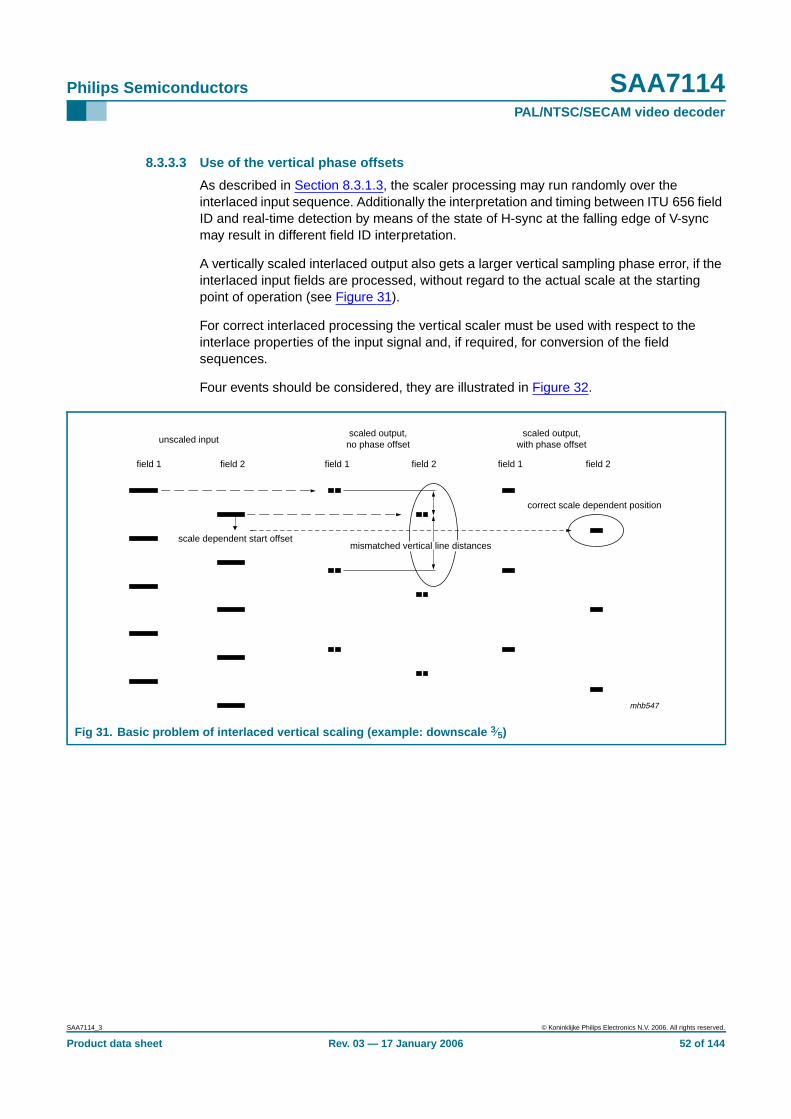
Philips Semiconductors SAA7114PAL/NTSC/SECAM video decoder
8.3.3.3 Use of the vertical phase offsets
As described in Section 8.3.1.3, the scaler processing may run randomly over theinterlaced input sequence. Additionally the interpretation and timing between ITU 656 fieldID and real-time detection by means of the state of H-sync at the falling edge of V-syncmay result in different field ID interpretation.
A vertically scaled interlaced output also gets a larger vertical sampling phase error, if theinterlaced input fields are processed, without regard to the actual scale at the startingpoint of operation (see Figure 31).
For correct interlaced processing the vertical scaler must be used with respect to theinterlace properties of the input signal and, if required, for conversion of the fieldsequences.
Four events should be considered, they are illustrated in Figure 32.
Fig 31. Basic problem of interlaced vertical scaling (example: downscale 3⁄5)
mhb547
mismatched vertical line distancesscale dependent start offset
correct scale dependent position
unscaled inputscaled output,
no phase offsetscaled output,
with phase offset
field 1 field 2 field 1 field 2 field 1 field 2
SAA7114_3 © Koninklijke Philips Electronics N.V. 2006. All rights reserved.
Product data sheet Rev. 03 — 17 January 2006 52 of 144
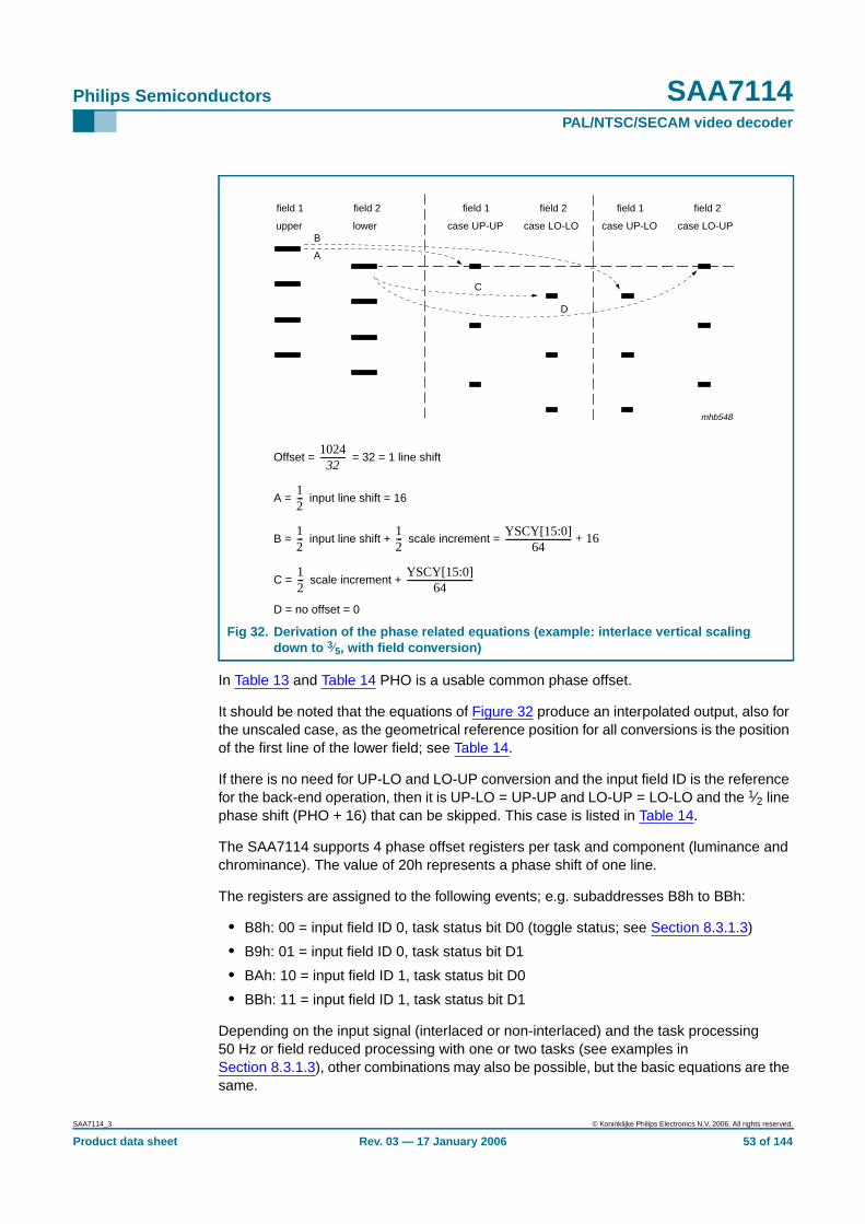
Philips Semiconductors SAA7114PAL/NTSC/SECAM video decoder
In Table 13 and Table 14 PHO is a usable common phase offset.
It should be noted that the equations of Figure 32 produce an interpolated output, also forthe unscaled case, as the geometrical reference position for all conversions is the positionof the first line of the lower field; see Table 14.
If there is no need for UP-LO and LO-UP conversion and the input field ID is the referencefor the back-end operation, then it is UP-LO = UP-UP and LO-UP = LO-LO and the 1⁄2 linephase shift (PHO + 16) that can be skipped. This case is listed in Table 14.
The SAA7114 supports 4 phase offset registers per task and component (luminance andchrominance). The value of 20h represents a phase shift of one line.
The registers are assigned to the following events; e.g. subaddresses B8h to BBh:
• B8h: 00 = input field ID 0, task status bit D0 (toggle status; see Section 8.3.1.3)
• B9h: 01 = input field ID 0, task status bit D1
• BAh: 10 = input field ID 1, task status bit D0
• BBh: 11 = input field ID 1, task status bit D1
Depending on the input signal (interlaced or non-interlaced) and the task processing50 Hz or field reduced processing with one or two tasks (see examples inSection 8.3.1.3), other combinations may also be possible, but the basic equations are thesame.
Offset = = 32 = 1 line shift
A = input line shift = 16
B = input line shift + scale increment =
C = scale increment +
D = no offset = 0
Fig 32. Derivation of the phase related equations (example: interlace vertical scalingdown to 3⁄5, with field conversion)
mhb548
field 1 field 2
upper lower
field 1 field 2
case UP-UP case LO-LO
field 1 field 2
case UP-LO case LO-UP
A
B
C
D
102432
------------
12---
12---
12---
YSCY[15:0]64
------------------------------ 16+
12---
YSCY[15:0]64
------------------------------
SAA7114_3 © Koninklijke Philips Electronics N.V. 2006. All rights reserved.
Product data sheet Rev. 03 — 17 January 2006 53 of 144
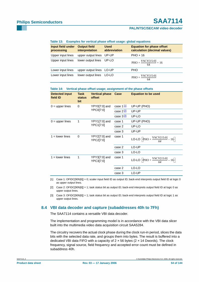
Philips Semiconductors SAA7114PAL/NTSC/SECAM video decoder
[1] Case 1: OFIDC[90h[6]] = 0; scaler input field ID as output ID; back-end interprets output field ID at logic 0as upper output lines.
[2] Case 2: OFIDC[90h[6]] = 1; task status bit as output ID; back-end interprets output field ID at logic 0 asupper output lines.
[3] Case 3: OFIDC[90h[6]] = 1; task status bit as output ID; back-end interprets output field ID at logic 1 asupper output lines.
8.4 VBI data decoder and capture (subaddresses 40h to 7Fh)The SAA7114 contains a versatile VBI data decoder.
The implementation and programming model is in accordance with the VBI data slicerbuilt into the multimedia video data acquisition circuit SAA5284.
The circuitry recovers the actual clock phase during the clock run-in period, slices the databits with the selected data rate, and groups them into bytes. The result is buffered into adedicated VBI data FIFO with a capacity of 2 × 56 bytes (2 × 14 Dwords). The clockfrequency, signal source, field frequency and accepted error count must be defined insubaddress 40h.
Table 13: Examples for vertical phase offset usage: global equations
Input field underprocessing
Output fieldinterpretation
Usedabbreviation
Equation for phase offsetcalculation (decimal values)
Upper input lines upper output lines UP-UP PHO + 16
Upper input lines lower output lines UP-LO
Lower input lines upper output lines LO-UP PHO
Lower input lines lower output lines LO-LO
Table 14: Vertical phase offset usage; assignment of the phase offsets
Detected inputfield ID
Taskstatusbit
Vertical phaseoffset
Case Equation to be used
0 = upper lines 0 YPY0[7:0] andYPC0[7:0]
case 1 [1] UP-UP (PHO)
case 2 [2] UP-UP
case 3 [3] UP-LO
0 = upper lines 1 YPY1[7:0] andYPC1[7:0]
case 1 UP-UP (PHO)
case 2 UP-LO
case 3 UP-UP
1 = lower lines 0 YPY2[7:0] andYPC2[7:0]
case 1LO-LO
case 2 LO-UP
case 3 LO-LO
1 = lower lines 1 YPY3[7:0] andYPC3[7:0]
case 1LO-LO
case 2 LO-LO
case 3 LO-UP
PHO YSCY[15:0]64
------------------------------ 16+ +
PHO YSCY[15:0]64
------------------------------+
PHO YSCY[15:0]64
------------------------------ 16–+
PHO YSCY[15:0]64
------------------------------ 16–+
SAA7114_3 © Koninklijke Philips Electronics N.V. 2006. All rights reserved.
Product data sheet Rev. 03 — 17 January 2006 54 of 144
Philips Semiconductors SAA7114PAL/NTSC/SECAM video decoder
The supported VBI data standards are shown in Table 15.
For lines 2 to 24 of a field, per VBI line, 1 of 16 standards can be selected (LCR24_[7:0] toLCR2_[7:0] in 57h[7:0] to 41h[7:0]: 23 × 2 × 4 bit programming bits).
The definition for line 24 is valid for the rest of the corresponding field, normally no textdata (video data) should be selected there (LCR24_[7:0] = FFh) to stop the activity of theVBI data slicer during active video.
To adjust the slicers processing to the input signal source, there are offsets in thehorizontal and vertical direction available: parameters HOFF[10:0] 5Bh[2:0] 59h[7:0],VOFF[8:0] 5Bh[4] 5Ah[7:0] and FOFF[5Bh[7]].
Contrary to the scalers counting, the slicers offsets define the position of the H and Vtrigger events related to the processed video field. The trigger events are the falling edgeof HREF and the falling edge of V123 from the decoder processing part.
The relationship of these programming values to the input signal and the recommendedvalues are given in Figure 22 and Figure 23.
8.5 Image port output formatter (subaddresses 84h to 87h)The output interface consists of a FIFO for video and for sliced text data, an arbitrationcircuit, which controls the mixed transfer of video and sliced text data over the I port and adecoding and multiplexing unit, which generates the 8-bit or 16-bit wide output datastream and the accompanied reference and supporting information.
Table 15: Data types supported by the data slicer block
DT[3:0]62h[3:0]
Standard type Data rate(Mbit/s)
Framing Code(FC)
FC window Hammingcheck
0000 teletext EuroWST, CCST 6.9375 27h WST625 always
0001 European closed caption 0.500 001 CC625
0010 VPS 5 9951h VPS
0011 wide screen signalling bits 5 1E 3C1Fh WSS
0100 US teletext (WST) 5.7272 27h WST525 always
0101 US closed caption (line 21) 0.503 001 CC525
0110 (video data selected) 5 none disable
0111 (raw data selected) 5 none disable
1000 teletext 6.9375 programmable general text optional
1001 VITC/EBU time codes(Europe)
1.8125 programmable VITC625
1010 VITC/SMPTE time codes(USA)
1.7898 programmable VITC525
1011 reserved
1100 US NABTS 5.7272 programmable NABTS optional
1101 MOJI (Japanese) 5.7272 programmable(A7h)
Japtext
1110 Japanese format switch(L20/22)
5 programmable open
1111 no sliced data transmitted(video data selected)
5 none disable
SAA7114_3 © Koninklijke Philips Electronics N.V. 2006. All rights reserved.
Product data sheet Rev. 03 — 17 January 2006 55 of 144
Philips Semiconductors SAA7114PAL/NTSC/SECAM video decoder
The clock for the output interface can be derived from an internal clock, decoder,expansion port, or an externally provided clock which is appropriate for e.g. VGA andframe buffer. The clock can be up to 33 MHz. The scaler provides the following videorelated timing reference events (signals), which are available on pins as defined bysubaddresses 84h and 85h:
• Output field ID
• Start and end of vertical active video range
• Start and end of active video line
• Data qualifier or gated clock
• Actually activated programming page (if CONLH is used)
• Threshold controlled FIFO filling flags (empty, full and filled)
• Sliced data marker
The discontinuous data stream at the scaler output is accompanied by a data valid flag (ordata qualifier), or is transported via a gated clock. Clock cycles with invalid data on theI port data bus (including the HPD pins in 16-bit output mode) are marked with code 00h.
The output interface also arbitrates the transfer between scaled video data and sliced textdata over the I port output.
The bits VITX1 and VITX0 (subaddress 86h) are used to control the arbitration.
As a further operation the serialization of the internal 32-bit Dwords to 8-bit or optional16-bit output, as well as the insertion of the extended ITU 656 codes (SAV/EAV for videodata, ANC or SAV/EAV codes for sliced text data) are done here.
For handshake with the VGA controller, or other memory or bus interface circuitry,programmable FIFO flags are provided; see Section 8.5.2.
8.5.1 Scaler output formatter (subaddresses 93h and C3h)
The output formatter organizes the packing into the output FIFO. The following formatsare available: Y-CB-CR 4 : 2 : 2, Y-CB-CR 4 : 1 : 1, Y-CB-CR 4 : 2 : 0, Y-CB-CR 4 : 1 : 0 andYonly (e.g. for raw samples). The formatting is controlled by FSI[2:0] 93h[2:0], FOI[1:0]93h[4:3] and FYSK[93h[5]].
The data formats are defined on Dwords, or multiples, and are similar to the video formatsas recommended for PCI multimedia applications (compares to SAA7146A), but planarformats are not supported.
FSI[2:0] defines the horizontal packing of the data, FOI[1:0] defines how many Yonly linesare expected, before a Y/C line will be formatted. If FYSK is set to logic 0 preceding Yonlylines will be skipped, and the output will always start with a Y/C line.
Additionally the output formatter limits the amplitude range of the video data (controlled byILLV[85h[5]]); see Table 18.
SAA7114_3 © Koninklijke Philips Electronics N.V. 2006. All rights reserved.
Product data sheet Rev. 03 — 17 January 2006 56 of 144
Philips Semiconductors SAA7114PAL/NTSC/SECAM video decoder
8.5.2 Video FIFO (subaddress 86h)
The video FIFO at the scaler output contains 32 Dwords. That corresponds to 64 pixels in16-bit Y-CB-CR 4 : 2 : 2 format. But as the entire scaler can act as a pipeline buffer, theactual available buffer capacity for the image port is much higher, and can exceed beyonda video line.
The image port, and the video FIFO, can operate with the video source clock(synchronous mode) or with an externally provided clock (asynchronous and burst mode),as appropriate for the VGA controller or attached frame buffer.
The video FIFO provides 4 internal flags, reporting to what extent the FIFO is actuallyfilled.
These are:
• The FIFO Almost Empty (FAE) flag
• The FIFO Combined Flag (FCF) or FIFO filled, which is set at almost full level andreset, with hysteresis, only after the level crosses below the almost empty mark
• The FIFO Almost Full (FAF) flag
• The FIFO Overflow (FOVL) flag
The trigger levels for FAE and FAF are programmable by FFL[1:0] 86h[3:2] (16, 24, 28,full) and FEL[1:0] 86h[1:0] (16, 8, 4, empty).
The state of this flag can be seen on pins IGP0 or IGP1. The pin mapping is defined bysubaddresses 84h and 85h; see Section 9.5.
Table 16: Byte stream for different output formats
Output format Byte sequence for 8-bit output modes
Y-CB-CR 4 : 2 : 2 CB0 Y0 CR0 Y1 CB2 Y2 CR2 Y3 CB4 Y4 CR4 Y5 CB6 Y6
Y-CB-CR 4 : 1 : 1 CB0 Y0 CR0 Y1 CB4 Y2 CR4 Y3 Y4 Y5 Y6 Y7 CB8 Y8
Yonly Y0 Y1 Y2 Y3 Y4 Y5 Y6 Y7 Y8 Y9 Y10 Y11 Y12 Y13
Table 17: Explanation to Table 16
Name Explanation
CBn CB (B − Y) color difference component, pixel number n = 0, 2, 4 to 718
Yn Y (luminance) component, pixel number n = 0, 1, 2, 3 to 719
CRn CR (R − Y) color difference component, pixel number n = 0, 2, 4 to 718
Table 18: Limiting range on I port
Limit stepILLV[85h[5]]
Valid range Suppressed codes (hexadecimal value)
Decimal value Hexadecimal value Lower range Upper range
0 1 to 254 01 to FE 00 FF
1 8 to 247 08 to F7 00 to 07 F8 to FF
SAA7114_3 © Koninklijke Philips Electronics N.V. 2006. All rights reserved.
Product data sheet Rev. 03 — 17 January 2006 57 of 144
Philips Semiconductors SAA7114PAL/NTSC/SECAM video decoder
8.5.3 Text FIFO
The data of the internal VBI data slicer is collected in the text FIFO before thetransmission over the I port is requested (normally before the video window starts). It ispartitioned into two FIFO sections. A complete line is filled into the FIFO before a datatransfer is requested. So normally, one line of text data is ready for transfer, while the nexttext line is collected. Thus sliced text data is delivered as a block of qualified data, withoutany qualification gaps in the byte stream of the I port.
The decoded VBI data is collected in the dedicated VBI data FIFO. After the capture of aline has been completed, the FIFO can be streamed through the image port, preceded bya header, giving line number and standard.
The VBI data period can be signalled via the sliced data flag on pin IGP0 or IGP1. Thedecoded VBI data is lead by the ITU ancillary data header (DID[5:0] 5Dh[5:0] at value< 3Eh) or by SAV/EAV codes selectable by DID[5:0] at value 3Eh or 3Fh. Pin IGP0 orIGP1 is set if the first byte of the ANC header is valid on the I port bus. It is reset if an SAVoccurs. So it may frame multiple lines of text data output, in the event that the videoprocessing starts with a distance of several video lines to the region of text data. Validsliced data from the text FIFO is available on the I port as long as the IGP0 or IGP1 flag isset and the data qualifier is active on pin IDQ.
The decoded VBI data is presented in two different data formats, controlled by bitRECODE.
• RECODE = 1: values 00h and FFh will be recoded to even parity values 03h and FCh
• RECODE = 0: values 00h and FFh may occur in the data stream as detected
8.5.4 Video and text arbitration (subaddress 86h)
Sliced text data and scaled video data are transferred over the same bus, the I port. Themixed transfer is controlled by an arbitration circuit.
If the video data is transferred without any interrupt and the video FIFO does not need tobuffer any output pixel, the text data is inserted after the end of a scaled video line,normally during the blanking interval of the video.
8.5.5 Data stream coding and reference signal generation (subaddresses 84h,85h and 93h)
As H and V reference signals are logic 1, active gate signals are generated, which framethe transfer of the valid output data. As an alternative to the gates, H and V trigger pulsesare generated on the rising edges of the gates.
Due to the dynamic FIFO behavior of the complete scaler path, the output signal timinghas no fixed timing relationship to the real-time input video stream. So fixed propagationdelays, in terms of clock cycles, related to the analog input cannot be defined.
The data stream is accompanied by a data qualifier. Additionally invalid data cycles aremarked with code 00h.
If ITU 656 like codes are not required, they can be suppressed in the output stream.
SAA7114_3 © Koninklijke Philips Electronics N.V. 2006. All rights reserved.
Product data sheet Rev. 03 — 17 January 2006 58 of 144
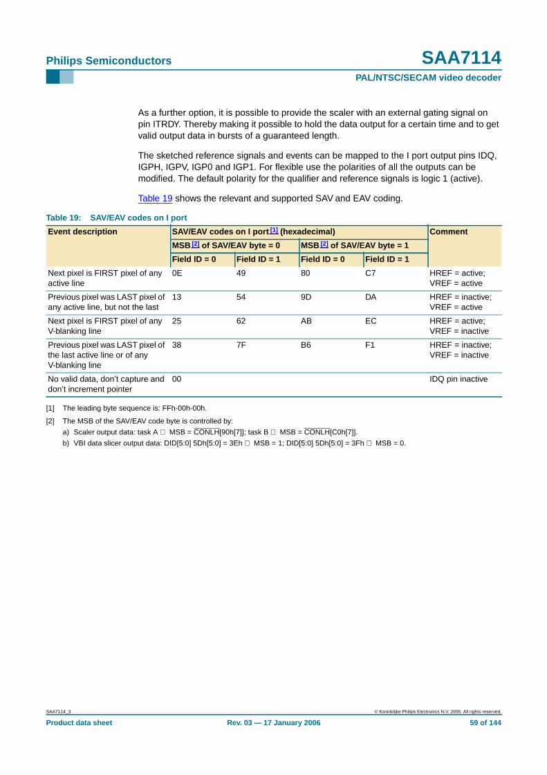
Philips Semiconductors SAA7114PAL/NTSC/SECAM video decoder
As a further option, it is possible to provide the scaler with an external gating signal onpin ITRDY. Thereby making it possible to hold the data output for a certain time and to getvalid output data in bursts of a guaranteed length.
The sketched reference signals and events can be mapped to the I port output pins IDQ,IGPH, IGPV, IGP0 and IGP1. For flexible use the polarities of all the outputs can bemodified. The default polarity for the qualifier and reference signals is logic 1 (active).
Table 19 shows the relevant and supported SAV and EAV coding.
[1] The leading byte sequence is: FFh-00h-00h.
[2] The MSB of the SAV/EAV code byte is controlled by:
a) Scaler output data: task A ⇒ MSB = CONLH[90h[7]]; task B ⇒ MSB = CONLH[C0h[7]].
b) VBI data slicer output data: DID[5:0] 5Dh[5:0] = 3Eh ⇒ MSB = 1; DID[5:0] 5Dh[5:0] = 3Fh ⇒ MSB = 0.
Table 19: SAV/EAV codes on I port
Event description SAV/EAV codes on I port [1] (hexadecimal) Comment
MSB [2] of SAV/EAV byte = 0 MSB [2] of SAV/EAV byte = 1
Field ID = 0 Field ID = 1 Field ID = 0 Field ID = 1
Next pixel is FIRST pixel of anyactive line
0E 49 80 C7 HREF = active;VREF = active
Previous pixel was LAST pixel ofany active line, but not the last
13 54 9D DA HREF = inactive;VREF = active
Next pixel is FIRST pixel of anyV-blanking line
25 62 AB EC HREF = active;VREF = inactive
Previous pixel was LAST pixel ofthe last active line or of anyV-blanking line
38 7F B6 F1 HREF = inactive;VREF = inactive
No valid data, don’t capture anddon’t increment pointer
00 IDQ pin inactive
SAA7114_3 © Koninklijke Philips Electronics N.V. 2006. All rights reserved.
Product data sheet Rev. 03 — 17 January 2006 59 of 144
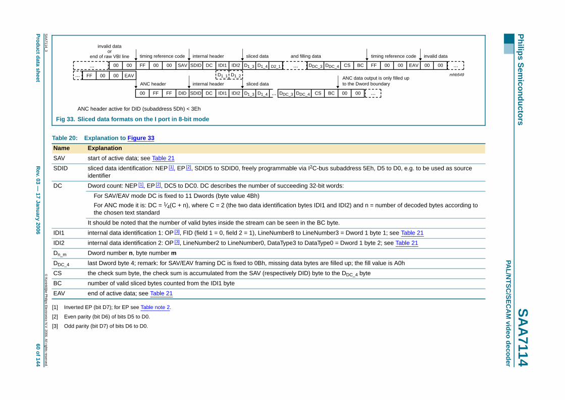
xxxxxxxxxxxxxxxxxxxxx xxxxxxxxxxxxxxxxxxxxxxxxxx xxxxxxx x x x xxxxxxxxxxxxxxxxxxxxxxxxxxxxxx xxxxxxxxxxxxxxxxxxx xx xxxxxxx xxxxxxxxxxxxxxxxxxxxxxxxxxx xxxxxxxxxxxxxxxxxxx xxxxxx xxxxxxxxxxxxxxxxxxxxxxxxxxxxxxxxxxx xxxxxxxxxxxx x xxxxxxxxxxxxxxxxxxxxxx xxxxxxxxxxxxxxxxxxxxxxxxxxxxxx xxxxx xxxxxxxxxxxxxxxxxxxxxxxxxxxxxxxxxxxxxxxxxxxxxxxxxx xxxxxxxxxxxxxxxxxxxxxxxxxxxxxxxxx xxxxxxxxxxxxxxxxxxxx xxx
SA
A7114_3
Product data shee
Philips S
emiconductors
SA
A7114
PAL/N
TS
C/S
EC
AM
video decoder
mhb549
00 00 FF 00 00 SAV SDID DC IDI1 IDI2 D1_3 D1_4 D2_1 DDC_3 DDC_4 CS BC FF 00 00 EAV 00 00... ...
..
...
ut is only filled upoundary
timing reference code
invalid dataor
end of raw VBI line timing reference codeinternal header sliced data invalid dataand filling data
, D5 to D0, e.g. to be used as source
number of decoded bytes according to
yte 1; see Table 21
e 2; see Table 21
value is A0h
© K
oninklijke Philips E
lectronics N.V. 2006. A
ll rights reserved.
tR
ev. 03 — 17 January 2006
60 of 144
[1] Inverted EP (bit D7); for EP see Table note 2.
[2] Even parity (bit D6) of bits D5 to D0.
[3] Odd parity (bit D7) of bits D6 to D0.
ANC header active for DID (subaddress 5Dh) < 3Eh
Fig 33. Sliced data formats on the I port in 8-bit mode
...
.
D1_2D1_1FF 00 00 EAV
00 FF FF DID SDID DC IDI1 IDI2 D1_3 D1_4 DDC_3 DDC_4 CS BC 00 00...
ANC header internal header sliced dataANC data outpto the Dword b
Table 20: Explanation to Figure 33
Name Explanation
SAV start of active data; see Table 21
SDID sliced data identification: NEP [1], EP [2], SDID5 to SDID0, freely programmable via I2C-bus subaddress 5Ehidentifier
DC Dword count: NEP [1], EP [2], DC5 to DC0. DC describes the number of succeeding 32-bit words:
For SAV/EAV mode DC is fixed to 11 Dwords (byte value 4Bh)
For ANC mode it is: DC = 1⁄4(C + n), where C = 2 (the two data identification bytes IDI1 and IDI2) and n =the chosen text standard
It should be noted that the number of valid bytes inside the stream can be seen in the BC byte.
IDI1 internal data identification 1: OP [3], FID (field 1 = 0, field 2 = 1), LineNumber8 to LineNumber3 = Dword 1 b
IDI2 internal data identification 2: OP [3], LineNumber2 to LineNumber0, DataType3 to DataType0 = Dword 1 byt
Dn_m Dword number n, byte number m
DDC_4 last Dword byte 4; remark: for SAV/EAV framing DC is fixed to 0Bh, missing data bytes are filled up; the fill
CS the check sum byte, the check sum is accumulated from the SAV (respectively DID) byte to the DDC_4 byte
BC number of valid sliced bytes counted from the IDI1 byte
EAV end of active data; see Table 21
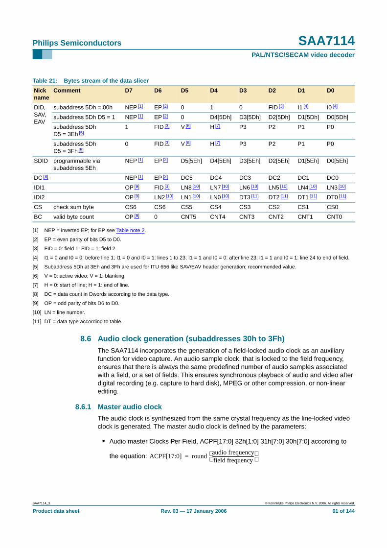
Philips Semiconductors SAA7114PAL/NTSC/SECAM video decoder
[1] NEP = inverted EP; for EP see Table note 2.
[2] EP = even parity of bits D5 to D0.
[3] FID = 0: field 1; FID = 1: field 2.
[4] I1 = 0 and I0 = 0: before line 1; I1 = 0 and I0 = 1: lines 1 to 23; I1 = 1 and I0 = 0: after line 23; I1 = 1 and I0 = 1: line 24 to end of field.
[5] Subaddress 5Dh at 3Eh and 3Fh are used for ITU 656 like SAV/EAV header generation; recommended value.
[6] V = 0: active video; V = 1: blanking.
[7] H = 0: start of line; H = 1: end of line.
[8] DC = data count in Dwords according to the data type.
[9] OP = odd parity of bits D6 to D0.
[10] LN = line number.
[11] DT = data type according to table.
8.6 Audio clock generation (subaddresses 30h to 3Fh)The SAA7114 incorporates the generation of a field-locked audio clock as an auxiliaryfunction for video capture. An audio sample clock, that is locked to the field frequency,ensures that there is always the same predefined number of audio samples associatedwith a field, or a set of fields. This ensures synchronous playback of audio and video afterdigital recording (e.g. capture to hard disk), MPEG or other compression, or non-linearediting.
8.6.1 Master audio clock
The audio clock is synthesized from the same crystal frequency as the line-locked videoclock is generated. The master audio clock is defined by the parameters:
• Audio master Clocks Per Field, ACPF[17:0] 32h[1:0] 31h[7:0] 30h[7:0] according to
the equation:
Table 21: Bytes stream of the data slicer
Nickname
Comment D7 D6 D5 D4 D3 D2 D1 D0
DID,SAV,EAV
subaddress 5Dh = 00h NEP [1] EP [2] 0 1 0 FID [3] I1 [4] I0 [4]
subaddress 5Dh D5 = 1 NEP [1] EP [2] 0 D4[5Dh] D3[5Dh] D2[5Dh] D1[5Dh] D0[5Dh]
subaddress 5DhD5 = 3Eh [5]
1 FID [3] V [6] H [7] P3 P2 P1 P0
subaddress 5DhD5 = 3Fh [5]
0 FID [3] V [6] H [7] P3 P2 P1 P0
SDID programmable viasubaddress 5Eh
NEP [1] EP [2] D5[5Eh] D4[5Eh] D3[5Eh] D2[5Eh] D1[5Eh] D0[5Eh]
DC [8] NEP [1] EP [2] DC5 DC4 DC3 DC2 DC1 DC0
IDI1 OP [9] FID [3] LN8 [10] LN7 [10] LN6 [10] LN5 [10] LN4 [10] LN3 [10]
IDI2 OP [9] LN2 [10] LN1 [10] LN0 [10] DT3 [11] DT2 [11] DT1 [11] DT0 [11]
CS check sum byte CS6 CS6 CS5 CS4 CS3 CS2 CS1 CS0
BC valid byte count OP [9] 0 CNT5 CNT4 CNT3 CNT2 CNT1 CNT0
ACPF[17:0] roundaudio frequencyfield frequency--------------------------------------
=
SAA7114_3 © Koninklijke Philips Electronics N.V. 2006. All rights reserved.
Product data sheet Rev. 03 — 17 January 2006 61 of 144
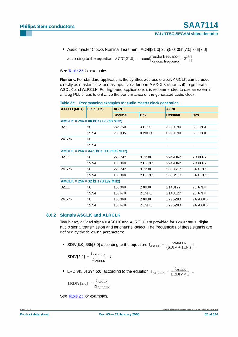
Philips Semiconductors SAA7114PAL/NTSC/SECAM video decoder
• Audio master Clocks Nominal Increment, ACNI[21:0] 36h[5:0] 35h[7:0] 34h[7:0]
according to the equation:
See Table 22 for examples.
Remark : For standard applications the synthesized audio clock AMCLK can be useddirectly as master clock and as input clock for port AMXCLK (short cut) to generateASCLK and ALRCLK. For high-end applications it is recommended to use an externalanalog PLL circuit to enhance the performance of the generated audio clock.
8.6.2 Signals ASCLK and ALRCLK
Two binary divided signals ASCLK and ALRCLK are provided for slower serial digitalaudio signal transmission and for channel-select. The frequencies of these signals aredefined by the following parameters:
• SDIV[5:0] 38h[5:0] according to the equation: ⇒
• LRDIV[5:0] 39h[5:0] according to the equation: ⇒
See Table 23 for examples.
Table 22: Programming examples for audio master clock generation
XTALO (MHz) Field (Hz) ACPF ACNI
Decimal Hex Decimal Hex
AMCLK = 256 × 48 kHz (12.288 MHz)
32.11 50 245760 3 C000 3210190 30 FBCE
59.94 205005 3 20CD 3210190 30 FBCE
24.576 50 - - - -
59.94 - - - -
AMCLK = 256 × 44.1 kHz (11.2896 MHz)
32.11 50 225792 3 7200 2949362 2D 00F2
59.94 188348 2 DFBC 2949362 2D 00F2
24.576 50 225792 3 7200 3853517 3A CCCD
59.94 188348 2 DFBC 3853 517 3A CCCD
AMCLK = 256 × 32 kHz (8.192 MHz)
32.11 50 163840 2 8000 2140127 20 A7DF
59.94 136670 2 15DE 2140127 20 A7DF
24.576 50 163840 2 8000 2796203 2A AAAB
59.94 136670 2 15DE 2796203 2A AAAB
ACNI[21:0] roundaudio frequencycrystal frequency----------------------------------------- 2
23× =
fASCLK
fAMXCLK
SDIV 1+( ) 2×-------------------------------------=
SDIV[5:0]fAMXCLK
2fASCLK--------------------- 1–=
fALRCLK
fASCLK
LRDIV 2×---------------------------=
LRDIV[5:0]fASCLK
2fALRCLK-----------------------=
SAA7114_3 © Koninklijke Philips Electronics N.V. 2006. All rights reserved.
Product data sheet Rev. 03 — 17 January 2006 62 of 144

Philips Semiconductors SAA7114PAL/NTSC/SECAM video decoder
8.6.3 Other control signals
Further control signals are available to define reference clock edges and verticalreferences; see Table 24.
Table 23: Programming examples for ASCLK/ALRCLK clock generation
AMXCLK(MHz)
ASCLK(kHz)
SDIV ALRCLK(kHz)
LRDIV
Decimal Hex Decimal Hex
12.288 1536 3 03 48 16 10
768 7 07 48 8 08
11.2896 1411.2 3 03 44.1 16 10
2822.4 1 01 44.1 32 10
8.192 1024 3 03 32 16 10
2048 1 01 32 32 10
Table 24: Control signals for reference clock edges and vertical references
Signal Description
APLL[3Ah[3]] Audio PLL mode
0 = PLL closed
1 = PLL open
AMVR[3Ah[2]] Audio Master clock Vertical Reference
0 = internal V
1 = external V
LRPH[3Ah[1]] ALRCLK phase
0 = invert ASCLK, ALRCLK edges triggered by falling edge of ASCLK
1 = don’t invert ASCLK, ALRCLK edges triggered by rising edge of ASCLK
SCPH[3Ah[0]] ASCLK phase
0 = invert AMXCLK, ASCLK edges triggered by falling edge of AMXCLK
1 = don’t invert AMXCLK, ASCLK edges triggered by rising edge of AMXCLK
SAA7114_3 © Koninklijke Philips Electronics N.V. 2006. All rights reserved.
Product data sheet Rev. 03 — 17 January 2006 63 of 144
Philips Semiconductors SAA7114PAL/NTSC/SECAM video decoder
9. Input/output interfaces and ports
The SAA7114 has 5 different I/O interfaces:
• Analog video input interface, for analog CVBS and/or Y and C input signals
• Audio clock port
• Digital real-time signal port (RT port)
• Digital video expansion port (X port), for unscaled digital video input and output
• Digital image port (I port) for scaled video data output and programming
• Digital host port (H port) for extension of the image port or expansion port from8-bit to 16-bit
9.1 Analog terminalsThe SAA7114 has 6 analog inputs AI21 to AI24, AI11 and AI12 for composite video CVBSor S-video Y/C signal pairs. Additionally, there are two differential reference inputs, whichmust be connected to ground via a capacitor equivalent to the decoupling capacitors atthe 6 inputs. There are no peripheral components required other than these decouplingcapacitors and 18 Ω/56 Ω termination resistors, one set per connected input signal; seeapplication example in Figure 53. Two anti-alias filters are integrated, and self adjustingvia the clock frequency.
Clamp and gain control for the two ADCs are also integrated. An analog video output(pin AOUT) is provided for testing purposes.
[1] Pin numbers for LQFP100 in parenthesis.
9.2 Audio clock signalsThe SAA7114 also synchronizes the audio clock and sampling rate to the video framerate, via a very slow PLL. This ensures that the multimedia capture and compressionprocesses always gather the same predefined number of samples per video frame.
An audio master clock AMCLK and two divided clocks ASCLK and ALRCLK aregenerated:
• ASCLK: can be used as audio serial clock
• ALRCLK: audio left/right channel clock
Table 25: Analog pin description
Symbol Pin [1] I/O Description Bit
AI24 to AI21 P6, P7, P9 and P10(10, 12, 14 and 16)
I analog video signal inputs, e.g.2 CVBS signals and two Y/C pairscan be connected simultaneously
MODE3 toMODE0
AI12 and AI11 P11 and P13(18 and 20)
I analog video signal inputs, e.g.2 CVBS signals and two Y/C pairscan be connected simultaneously
MODE3 toMODE0
AOUT M10 (22) O analog video output, for testpurposes
AOSL1 andAOSL0
AI1D and AI2D P12 and P8(19 and 13)
I analog reference pins for differentialADC operation
-
SAA7114_3 © Koninklijke Philips Electronics N.V. 2006. All rights reserved.
Product data sheet Rev. 03 — 17 January 2006 64 of 144
Philips Semiconductors SAA7114PAL/NTSC/SECAM video decoder
The ratios are programmable; see Section 8.6.
[1] Pin numbers for LQFP100 in parenthesis.
9.3 Clock and real-time synchronization signalsFor the generation of the line-locked video (pixel) clock LLC, and of the frame-lockedaudio serial bit clock, a crystal accurate frequency reference is required. An oscillator isbuilt-in for fundamental or third harmonic crystals. The supported crystal frequencies are32.11 MHz or 24.576 MHz (defined during reset by strapping pin ALRCLK).
Alternatively pin XTALI can be driven from an external single-ended oscillator.
The crystal oscillation can be propagated as a clock to other ICs in the system viapin XTOUT.
The Line-Locked Clock (LLC) is the double pixel clock of nominal 27 MHz. It is locked tothe selected video input, generating baseband video pixels according to “ITUrecommendation 601”. In order to support interfacing circuits, a direct pixel clock (LLC2) isalso provided.
The pins for line and field timing reference signals are RTCO, RTS1 and RTS0. Variousreal-time status information can be selected for the RTS pins. The signals are alwaysavailable (output) and reflect the synchronization operation of the decoder part in theSAA7114. The function of the RTS1 and RTS0 pins can be defined by bits RTSE1[3:0]12h[7:4] and RTSE0[3:0] 12h[3:0].
Table 26: Audio clock pin description
Symbol Pin [1] I/O Description Bit
AMCLK K12(37)
O audio master clock output ACPF[17:0] 32h[1:0] 31h[7:0] 30h[7:0] andACNI[21:0] 36h[5:0] 35h[7:0] 34h[7:0]
AMXCLK J12(41)
I external audio master clockinput for the clock divisioncircuit, can be directlyconnected to outputAMCLK for standardapplications
-
ASCLK K14(39)
O serial audio clock output,can be synchronized torising or falling edge ofAMXCLK
SDIV[5:0] 38h[5:0] and SCPH[3Ah[0]]
ALRCLK J13(40)
O audio channel (left/right)clock output, can besynchronized to rising orfalling edge of ASCLK
LRDIV[5:0] 39h[5:0] and LRPH[3Ah[1]]
Table 27: Clock and real-time synchronization signals
Symbol Pin [1] I/O Description Bit
Crystal oscillator
XTALI P2(7)
I input for crystal oscillator or reference clock -
XTALO P3(6)
O output of crystal oscillator -
SAA7114_3 © Koninklijke Philips Electronics N.V. 2006. All rights reserved.
Product data sheet Rev. 03 — 17 January 2006 65 of 144
Philips Semiconductors SAA7114PAL/NTSC/SECAM video decoder
[1] Pin numbers for LQFP100 in parenthesis.
9.4 Video expansion port (X port)The expansion port is intended for transporting video streams image data from otherdigital video circuits such as MPEG encoder/decoder and video phone codec, to theimage port (I port).
The expansion port consists of two groups of signals/pins:
• 8-bit data, I/O, regularly components video Y-CB-CR 4 : 2 : 2, i.e. CB-Y-CR-Y, byteserial, exceptionally raw video samples (e.g. ADC test); in input mode the data buscan be extended to 16-bit by pins HPD7 to HPD0.
• Clock, synchronization and auxiliary signals, accompanying the data stream, I/O
As output, these are direct copies of the decoder signals.
The data transfers through the expansion port represent a single D1 port, with half duplexmode. The SAV and EAV codes may be inserted optionally for data input (controlled bybit XCODE[92h[3]]). The input/output direction is switched for complete fields only.
XTOUT P4(4)
O reference (crystal) clock output drive (optional) XTOUTE[14h[3]]
Real-time signals (RT port)
LLC M14(28)
O line-locked clock, nominal 27 MHz, double pixelclock locked to the selected video input signal
-
LLC2 L14(29)
O line-locked pixel clock, nominal 13.5 MHz -
RTCO L13(36)
O real-time control output, transfers real-time statusinformation supporting RTC level 3.1 (seedocument “RTC Functional Description”, availableon request)
-
RTS0 K13(34)
O real-time status information line 0, can beprogrammed to carry various real-timeinformation; see Table 56
RTSE0[3:0] 12h[3:0]
RTS1 L10(35)
O real-time status information line 1, can beprogrammed to carry various real-timeinformation; see Table 57
RTSE1[3:0] 12h[7:4]
Table 27: Clock and real-time synchronization signals …continued
Symbol Pin [1] I/O Description Bit
SAA7114_3 © Koninklijke Philips Electronics N.V. 2006. All rights reserved.
Product data sheet Rev. 03 — 17 January 2006 66 of 144
Philips Semiconductors SAA7114PAL/NTSC/SECAM video decoder
[1] Pin numbers for LQFP100 in parenthesis.
9.4.1 X port configured as output
If data output is enabled at the expansion port, then the data stream from the decoder ispresented. The data format of the 8-bit data bus is dependent on the chosen data type,selectable by the line control registers LCR2 to LCR24; see Table 7. In contrast to theimage port, the sliced data format is not available on the expansion port. Instead, rawCVBS samples are always transferred if any sliced data type is selected.
Some details of data types on the expansion port are as follows:
• Active video (data type 15): contains component Y-CB-CR 4 : 2 : 2 signal, 720 activepixels per line. The amplitude and offsets are programmable via DBRI7 to DBRI0,DCON7 to DCON0, DSAT7 to DSAT0, OFFU1, OFFU0, OFFV1 and OFFV0. Thenominal levels are illustrated in Figure 18.
• Test line (data type 6): is similar to the active video format, with some constraintswithin the data processing:
– Adaptive chrominance comb filter, vertical filter (chrominance comb filter for NTSCstandards, PAL phase error correction) within the chrominance processing aredisabled
Table 28: Signals dedicated to the expansion port
Symbol Pin [1] I/O Description Bit
XPD7 toXPD0
K2, K3, L1 toL3, M1, M2and N1(81, 82, 84 to87, 89 and 90)
I/O X port data: in output mode controlled bydecoder section, data format see Table 29;in input mode Y-CB-CR 4 : 2 : 2 serial inputdata or luminance part of a 16-bitY-CB-CR 4 : 2 : 2 input
OFTS[2:0] 13h[2:0],91h[7:0] andC1h[7:0]
XCLK M3 (94) I/O clock at expansion port: if output, thencopy of LLC; as input normally a doublepixel clock of up to 32 MHz or a gatedclock (clock gated with a qualifier)
XCKS[92h[0]]
XDQ M4 (95) I/O data valid flag of the expansion port input(qualifier): if output, then decoder(HREF and VGATE) gate; see Figure 26
-
XRDY N3 (96) O data request flag = ready to receive, towork with optional buffer in externaldevice, to prevent internal buffer overflow;second function: input related task flagA/B
XRQT[83h[2]]
XRH N2 (92) I/O horizontal reference signal for the X port:as output: HREF or HS from the decoder(see Figure 26); as input: a reference edgefor horizontal input timing and a polarity forinput field ID detection can be defined
XRHS[13h[6],XFDH[92h[6]] andXDH[92h[2]]
XRV L5 (91) I/O vertical reference signal for the X port: asoutput: V123 or field ID from the decoder(see Figure 24 and Figure 25); as input: areference edge for vertical input timing andfor input field ID detection can be defined
XRVS[1:0] 13h[5:4],XFDV[92h[7]] andXDV[1:0] 92h[5:4]
XTRI K1 (80) I port control: switches X port input 3-state XPE[1:0] 83h[1:0]
SAA7114_3 © Koninklijke Philips Electronics N.V. 2006. All rights reserved.
Product data sheet Rev. 03 — 17 January 2006 67 of 144
Philips Semiconductors SAA7114PAL/NTSC/SECAM video decoder
– Adaptive luminance comb filter, peaking and chrominance trap are bypassed withinthe luminance processing
This data type is defined for future enhancements. It could be activated for linescontaining standard test signals within the vertical blanking period. Currently the mostsources do not contain test lines. The nominal levels are illustrated in Figure 18.
• Raw samples (data types 0 to 5 and 7 to 14): CB-CR samples are similar to datatype 6, but CVBS samples are transferred instead of processed luminance sampleswithin the Y time slots.
The amplitude and offset of the CVBS signal is programmable via RAWG7 to RAWG0and RAWO7 to RAWO0; see Section 10, Table 63 and Table 64. The nominal levelsare illustrated in Figure 19.
The relationship of LCR programming to line numbers is described in Section 8.2,Figure 22 and Figure 23.
The data type selections by LCR are overruled by setting OFTS2 = 1 (subaddress 13hbit D2). This setting is mainly intended for device production test. The VPO-bus carries theupper or lower 8 bits of the two ADCs depending on the OFTS[1:0] 13h[1:0] settings; seeTable 58. The input configuration is done via MODE[3:0] 02h[3:0] settings; see Table 40. Ifa Y/C mode is selected, the expansion port carries the multiplexed output signals of bothADCs, and in CVBS mode the output of only one ADC. No timing reference codes aregenerated in this mode.
Remark : The LSBs (bit D0) of the ADCs are also available on pin RTS0; see Table 56.
The SAV/EAV timing reference codes define the start and end of valid data regions. TheITU-blanking code sequence ‘- 80 - 10 - 80 - 10 -...’ is transmitted during the horizontalblanking period between EAV and SAV.
The position of the F-bit is constant in accordance with ITU 656; see Table 31 andTable 32.
The V-bit can be generated in two different ways (see Table 31 and Table 32) controlledvia OFTS1 and OFTS0; see Table 58.
The F and V bits change synchronously with the EAV code.
[1] The generation of the timing reference codes can be suppressed by setting OFTS[2:0] to 010; see Table 58. In this event the codesequence is replaced by the standard ‘- 80 - 10 -’ blanking values.
[2] If raw samples or sliced data are selected by the line control registers (LCR2 to LCR24), the Y samples are replaced by CVBS samples.
Table 29: Data format on the expansion port
Blankingperiod
Timing referencecode (Hex) [1]
720 pixels Y-C B-CR 4 : 2 : 2 data [2] Timing referencecode (Hex) [1]
Blankingperiod
... 80 10 FF 00 00 SAV CB0 Y0 CR0 Y1 CB2 Y2 ... CR718 Y719 FF 00 00 EAV 80 10 ...
SAA7114_3 © Koninklijke Philips Electronics N.V. 2006. All rights reserved.
Product data sheet Rev. 03 — 17 January 2006 68 of 144
Philips Semiconductors SAA7114PAL/NTSC/SECAM video decoder
Table 30: SAV/EAV format on expansion port XPD7 to XPD0
Bit Symbol Description
7 logic 1
6 F field bit
1st field: F = 0
2nd field: F = 1
for vertical timing see Table 31 and Table 32
5 V vertical blanking bit
VBI: V = 1
active video: V = 0
for vertical timing see Table 31 and Table 32
4 H format
H = 0 in SAV format
H = 1 in EAV format
3 to 0 P[3:0] reserved; evaluation not recommended (protection bits according toITU-R BT 656)
Table 31: 525 lines/60 Hz vertical timing
Line number F (ITU 656) V
OFTS[2:0] = 000(ITU 656)
OFTS[2:0] = 001
1 to 3 1 1 according to selected VGATE positiontype via VSTA and VSTO(subaddresses 15h to 17h);see Table 60 to Table 62
4 to 19 0 1
20 0 0
21 0 0
22 to 261 0 0
262 0 0
263 0 0
264 and 265 0 1
266 to 282 1 1
283 1 0
284 1 0
285 to 524 1 0
525 1 0
SAA7114_3 © Koninklijke Philips Electronics N.V. 2006. All rights reserved.
Product data sheet Rev. 03 — 17 January 2006 69 of 144
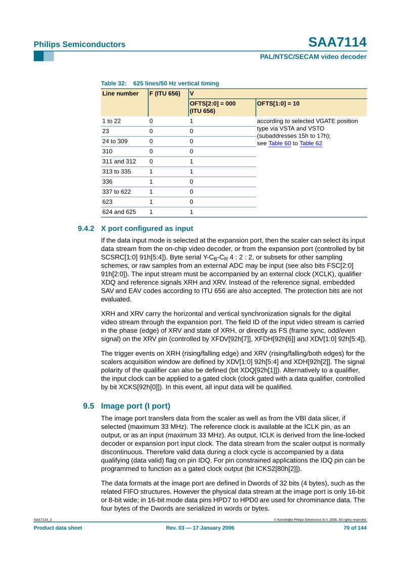
Philips Semiconductors SAA7114PAL/NTSC/SECAM video decoder
9.4.2 X port configured as input
If the data input mode is selected at the expansion port, then the scaler can select its inputdata stream from the on-chip video decoder, or from the expansion port (controlled by bitSCSRC[1:0] 91h[5:4]). Byte serial Y-CB-CR 4 : 2 : 2, or subsets for other samplingschemes, or raw samples from an external ADC may be input (see also bits FSC[2:0]91h[2:0]). The input stream must be accompanied by an external clock (XCLK), qualifierXDQ and reference signals XRH and XRV. Instead of the reference signal, embeddedSAV and EAV codes according to ITU 656 are also accepted. The protection bits are notevaluated.
XRH and XRV carry the horizontal and vertical synchronization signals for the digitalvideo stream through the expansion port. The field ID of the input video stream is carriedin the phase (edge) of XRV and state of XRH, or directly as FS (frame sync, odd/evensignal) on the XRV pin (controlled by XFDV[92h[7]], XFDH[92h[6]] and XDV[1:0] 92h[5:4]).
The trigger events on XRH (rising/falling edge) and XRV (rising/falling/both edges) for thescalers acquisition window are defined by XDV[1:0] 92h[5:4] and XDH[92h[2]]. The signalpolarity of the qualifier can also be defined (bit XDQ[92h[1]]). Alternatively to a qualifier,the input clock can be applied to a gated clock (clock gated with a data qualifier, controlledby bit XCKS[92h[0]]). In this event, all input data will be qualified.
9.5 Image port (I port)The image port transfers data from the scaler as well as from the VBI data slicer, ifselected (maximum 33 MHz). The reference clock is available at the ICLK pin, as anoutput, or as an input (maximum 33 MHz). As output, ICLK is derived from the line-lockeddecoder or expansion port input clock. The data stream from the scaler output is normallydiscontinuous. Therefore valid data during a clock cycle is accompanied by a dataqualifying (data valid) flag on pin IDQ. For pin constrained applications the IDQ pin can beprogrammed to function as a gated clock output (bit ICKS2[80h[2]]).
The data formats at the image port are defined in Dwords of 32 bits (4 bytes), such as therelated FIFO structures. However the physical data stream at the image port is only 16-bitor 8-bit wide; in 16-bit mode data pins HPD7 to HPD0 are used for chrominance data. Thefour bytes of the Dwords are serialized in words or bytes.
Table 32: 625 lines/50 Hz vertical timing
Line number F (ITU 656) V
OFTS[2:0] = 000(ITU 656)
OFTS[1:0] = 10
1 to 22 0 1 according to selected VGATE positiontype via VSTA and VSTO(subaddresses 15h to 17h);see Table 60 to Table 62
23 0 0
24 to 309 0 0
310 0 0
311 and 312 0 1
313 to 335 1 1
336 1 0
337 to 622 1 0
623 1 0
624 and 625 1 1
SAA7114_3 © Koninklijke Philips Electronics N.V. 2006. All rights reserved.
Product data sheet Rev. 03 — 17 January 2006 70 of 144
Philips Semiconductors SAA7114PAL/NTSC/SECAM video decoder
Available formats are as follows:
• Y-CB-CR 4 : 2 : 2
• Y-CB-CR 4 : 1 : 1
• Raw samples
• Decoded VBI data
For handshake with the receiving VGA controller, or other memory or bus interfacecircuitry, F, H and V reference signals and programmable FIFO flags are provided. Theinformation is provided on pins IGP0, IGP1, IGPH and IGPV. The functionality on thesepins is controlled via subaddresses 84h and 85h.
VBI data is collected over an entire line in its own FIFO, and transferred as anuninterrupted block of bytes. Decoded VBI data can be signed by the VBI flag on pin IGP0or IGP1.
As scaled video data and decoded VBI data may come from different and asynchronoussources, an arbitration scheme is needed. Normally the VBI data slicer has priority.
The image port consists of the pins and/or signals, as listed in Table 33.
For pin constrained applications, or interfaces, the relevant timing and data referencesignals can also get encoded into the data stream. Therefore the corresponding pins donot need to be connected. The minimum image port configuration requires 9 pins only, i.e.8 pins for data including codes, and 1 pin for clock or gated clock. The inserted codes aredefined in close relationship to the ITU-R BT.656 (D1) recommendation, where possible.
The following deviations from “ITU 656 recommendation” are implemented at theSAA7114 image port interface:
• SAV and EAV codes are only present in those lines, where data is to be transferred,i.e. active video lines, or VBI raw samples, no codes for empty lines
• There may be more or less than 720 pixels between SAV and EAV
• Data content and the number of clock cycles during horizontal and vertical blanking isundefined, and may not be constant
• Data stream may be interleaved with not-valid data codes, 00h, but SAV and EAV4-byte codes are not interleaved with not-valid data codes
• There may be an irregular pattern of not-valid data, or IDQ, and as a result, CB-Y-CR-Yis not in a fixed phase to a regular clock divider
• VBI raw sample streams are enveloped with SAV and EAV, like normal video
• Decoded VBI data is transported as Ancillary (ANC) data, two modes:
– Direct decoded VBI data bytes (8-bit) are directly placed in the ANC data field,00h and FFh codes may appear in data block (violation to ITU-R BT.656)
– Recoded VBI data bytes (8-bit) directly placed in ANC data field, 00h and FFhcodes will be recoded to even parity codes 03h and FCh to suppress invalidITU-R BT.656 codes
SAA7114_3 © Koninklijke Philips Electronics N.V. 2006. All rights reserved.
Product data sheet Rev. 03 — 17 January 2006 71 of 144
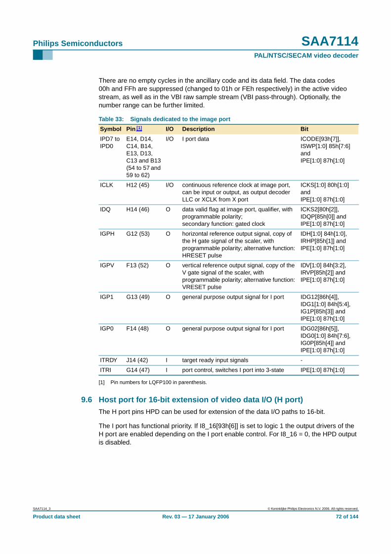
Philips Semiconductors SAA7114PAL/NTSC/SECAM video decoder
There are no empty cycles in the ancillary code and its data field. The data codes00h and FFh are suppressed (changed to 01h or FEh respectively) in the active videostream, as well as in the VBI raw sample stream (VBI pass-through). Optionally, thenumber range can be further limited.
[1] Pin numbers for LQFP100 in parenthesis.
9.6 Host port for 16-bit extension of video data I/O (H port)The H port pins HPD can be used for extension of the data I/O paths to 16-bit.
The I port has functional priority. If I8_16[93h[6]] is set to logic 1 the output drivers of theH port are enabled depending on the I port enable control. For I8_16 = 0, the HPD outputis disabled.
Table 33: Signals dedicated to the image port
Symbol Pin [1] I/O Description Bit
IPD7 toIPD0
E14, D14,C14, B14,E13, D13,C13 and B13(54 to 57 and59 to 62)
I/O I port data ICODE[93h[7]],ISWP[1:0] 85h[7:6]andIPE[1:0] 87h[1:0]
ICLK H12 (45) I/O continuous reference clock at image port,can be input or output, as output decoderLLC or XCLK from X port
ICKS[1:0] 80h[1:0]andIPE[1:0] 87h[1:0]
IDQ H14 (46) O data valid flag at image port, qualifier, withprogrammable polarity;secondary function: gated clock
ICKS2[80h[2]],IDQP[85h[0]] andIPE[1:0] 87h[1:0]
IGPH G12 (53) O horizontal reference output signal, copy ofthe H gate signal of the scaler, withprogrammable polarity; alternative function:HRESET pulse
IDH[1:0] 84h[1:0],IRHP[85h[1]] andIPE[1:0] 87h[1:0]
IGPV F13 (52) O vertical reference output signal, copy of theV gate signal of the scaler, withprogrammable polarity; alternative function:VRESET pulse
IDV[1:0] 84h[3:2],IRVP[85h[2]] andIPE[1:0] 87h[1:0]
IGP1 G13 (49) O general purpose output signal for I port IDG12[86h[4]],IDG1[1:0] 84h[5:4],IG1P[85h[3]] andIPE[1:0] 87h[1:0]
IGP0 F14 (48) O general purpose output signal for I port IDG02[86h[5]],IDG0[1:0] 84h[7:6],IG0P[85h[4]] andIPE[1:0] 87h[1:0]
ITRDY J14 (42) I target ready input signals -
ITRI G14 (47) I port control, switches I port into 3-state IPE[1:0] 87h[1:0]
SAA7114_3 © Koninklijke Philips Electronics N.V. 2006. All rights reserved.
Product data sheet Rev. 03 — 17 January 2006 72 of 144
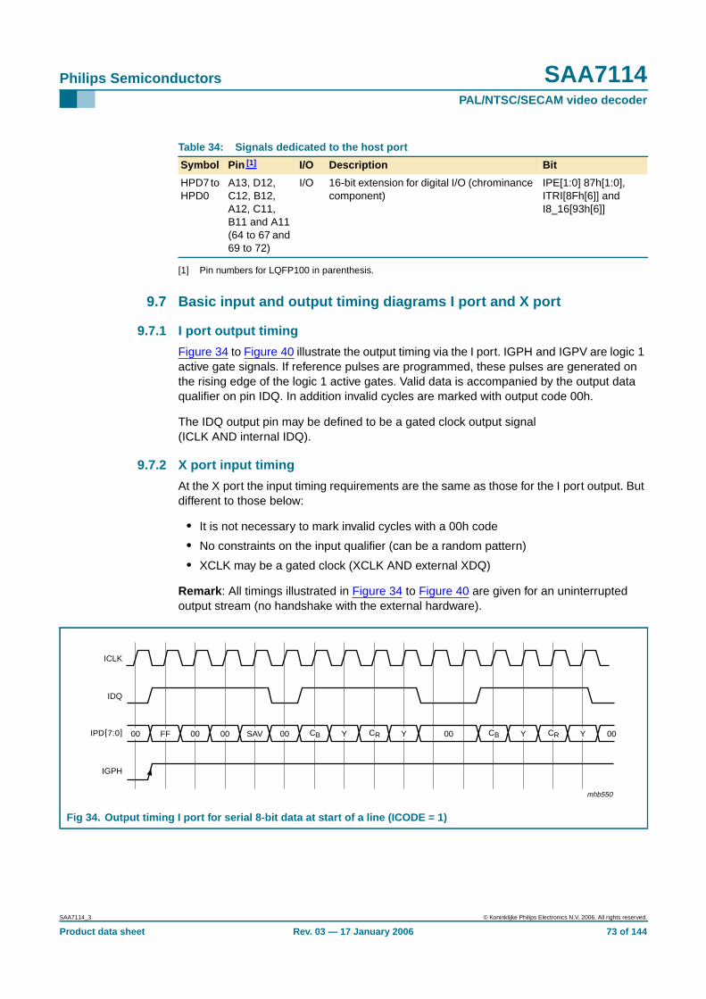
Philips Semiconductors SAA7114PAL/NTSC/SECAM video decoder
[1] Pin numbers for LQFP100 in parenthesis.
9.7 Basic input and output timing diagrams I port and X port
9.7.1 I port output timing
Figure 34 to Figure 40 illustrate the output timing via the I port. IGPH and IGPV are logic 1active gate signals. If reference pulses are programmed, these pulses are generated onthe rising edge of the logic 1 active gates. Valid data is accompanied by the output dataqualifier on pin IDQ. In addition invalid cycles are marked with output code 00h.
The IDQ output pin may be defined to be a gated clock output signal(ICLK AND internal IDQ).
9.7.2 X port input timing
At the X port the input timing requirements are the same as those for the I port output. Butdifferent to those below:
• It is not necessary to mark invalid cycles with a 00h code
• No constraints on the input qualifier (can be a random pattern)
• XCLK may be a gated clock (XCLK AND external XDQ)
Remark : All timings illustrated in Figure 34 to Figure 40 are given for an uninterruptedoutput stream (no handshake with the external hardware).
Table 34: Signals dedicated to the host port
Symbol Pin [1] I/O Description Bit
HPD7 toHPD0
A13, D12,C12, B12,A12, C11,B11 and A11(64 to 67 and69 to 72)
I/O 16-bit extension for digital I/O (chrominancecomponent)
IPE[1:0] 87h[1:0],ITRI[8Fh[6]] andI8_16[93h[6]]
Fig 34. Output timing I port for serial 8-bit data at start of a line (ICODE = 1)
IPD[7:0]
IGPH
IDQ
ICLK
00 FF 00 00 SAV 00 CB Y CR Y 00 CB Y CR Y 00
mhb550
SAA7114_3 © Koninklijke Philips Electronics N.V. 2006. All rights reserved.
Product data sheet Rev. 03 — 17 January 2006 73 of 144
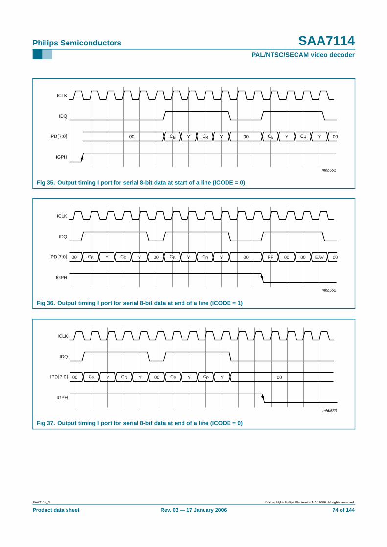
Philips Semiconductors SAA7114PAL/NTSC/SECAM video decoder
Fig 35. Output timing I port for serial 8-bit data at start of a line (ICODE = 0)
IPD[7:0]
IGPH
IDQ
ICLK
00 CB Y CR Y 00 CB Y CR Y 00
mhb551
Fig 36. Output timing I port for serial 8-bit data at end of a line (ICODE = 1)
IPD[7:0]
IGPH
IDQ
ICLK
00 CB Y CR Y 00 CB Y CR Y 00 FF 00 00 EAV 00
mhb552
Fig 37. Output timing I port for serial 8-bit data at end of a line (ICODE = 0)
IPD[7:0]
IGPH
IDQ
ICLK
00 CB Y CR Y 00 CB Y CR Y 00
mhb553
SAA7114_3 © Koninklijke Philips Electronics N.V. 2006. All rights reserved.
Product data sheet Rev. 03 — 17 January 2006 74 of 144
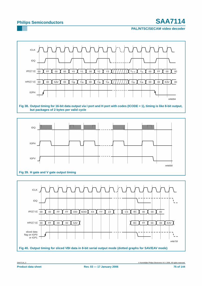
Philips Semiconductors SAA7114PAL/NTSC/SECAM video decoder
Fig 38. Output timing for 16-bit data output via I port and H port with codes (ICODE = 1), timing is like 8-bit output,but packages of 2 bytes per valid cycle
IPD[7:0]
HPD[7:0]
IGPH
IDQ
ICLK
00 FF 00 00 Y0 Y1 00 Y2 Y3 Yn−1 Yn 00 FF 00 00
mhb554
00 00 SAV 00 00 CBCB CRCR CRCB 00 00 EAV 00
Fig 39. H gate and V gate output timing
IGPV
IGPH
IDQ
mhb555
Fig 40. Output timing for sliced VBI data in 8-bit serial output mode (dotted graphs for SAV/EAV mode)
mhb733
IPD[7:0]
HPD[7:0]
sliced dataflag on IGP0
or IGP1
IDQ
ICLK
00 00 FF FF DID SDID XX YY ZZ CS BC 00 00 00
00 FF 00 SAV00 00 00BC FF EAV
SAA7114_3 © Koninklijke Philips Electronics N.V. 2006. All rights reserved.
Product data sheet Rev. 03 — 17 January 2006 75 of 144
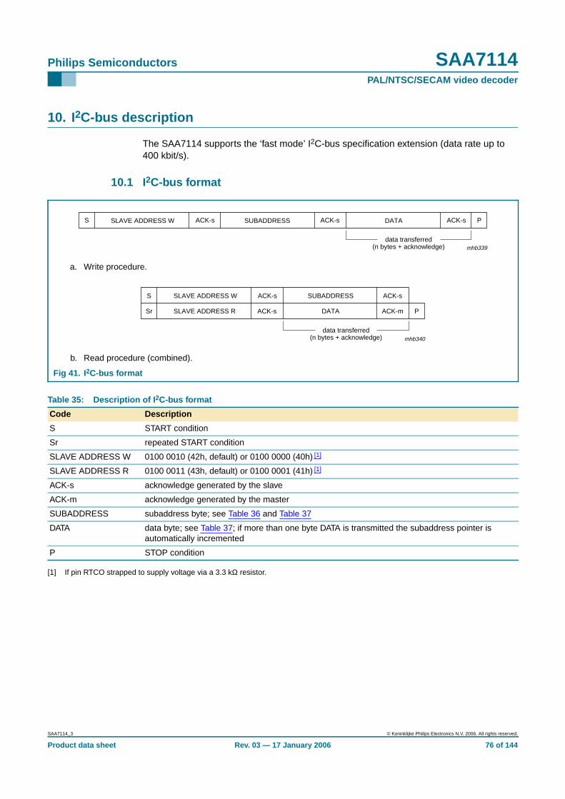
Philips Semiconductors SAA7114PAL/NTSC/SECAM video decoder
10. I2C-bus description
The SAA7114 supports the ‘fast mode’ I2C-bus specification extension (data rate up to400 kbit/s).
10.1 I2C-bus format
[1] If pin RTCO strapped to supply voltage via a 3.3 kΩ resistor.
a. Write procedure.
b. Read procedure (combined).
Fig 41. I2C-bus format
ACK-s ACK-sDATASLAVE ADDRESS W
data transferred(n bytes + acknowledge) mhb339
PS ACK-sSUBADDRESS
ACK-s ACK-mSLAVE ADDRESS R
mhb340
PSr
ACK-s ACK-s
DATA
SUBADDRESSSLAVE ADDRESS WS
data transferred(n bytes + acknowledge)
Table 35: Description of I 2C-bus format
Code Description
S START condition
Sr repeated START condition
SLAVE ADDRESS W 0100 0010 (42h, default) or 0100 0000 (40h) [1]
SLAVE ADDRESS R 0100 0011 (43h, default) or 0100 0001 (41h) [1]
ACK-s acknowledge generated by the slave
ACK-m acknowledge generated by the master
SUBADDRESS subaddress byte; see Table 36 and Table 37
DATA data byte; see Table 37; if more than one byte DATA is transmitted the subaddress pointer isautomatically incremented
P STOP condition
SAA7114_3 © Koninklijke Philips Electronics N.V. 2006. All rights reserved.
Product data sheet Rev. 03 — 17 January 2006 76 of 144
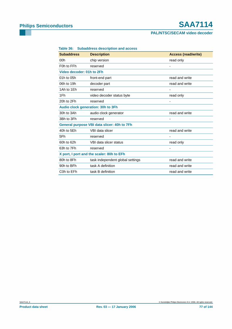
Philips Semiconductors SAA7114PAL/NTSC/SECAM video decoder
Table 36: Subaddress description and access
Subaddress Description Access (read/write)
00h chip version read only
F0h to FFh reserved -
Video decoder: 01h to 2Fh
01h to 05h front-end part read and write
06h to 19h decoder part read and write
1Ah to 1Eh reserved -
1Fh video decoder status byte read only
20h to 2Fh reserved -
Audio clock generation: 30h to 3Fh
30h to 3Ah audio clock generator read and write
3Bh to 3Fh reserved -
General purpose VBI data slicer: 40h to 7Fh
40h to 5Eh VBI data slicer read and write
5Fh reserved -
60h to 62h VBI data slicer status read only
63h to 7Fh reserved -
X port, I port and the scaler: 80h to EFh
80h to 8Fh task independent global settings read and write
90h to BFh task A definition read and write
C0h to EFh task B definition read and write
SAA7114_3 © Koninklijke Philips Electronics N.V. 2006. All rights reserved.
Product data sheet Rev. 03 — 17 January 2006 77 of 144
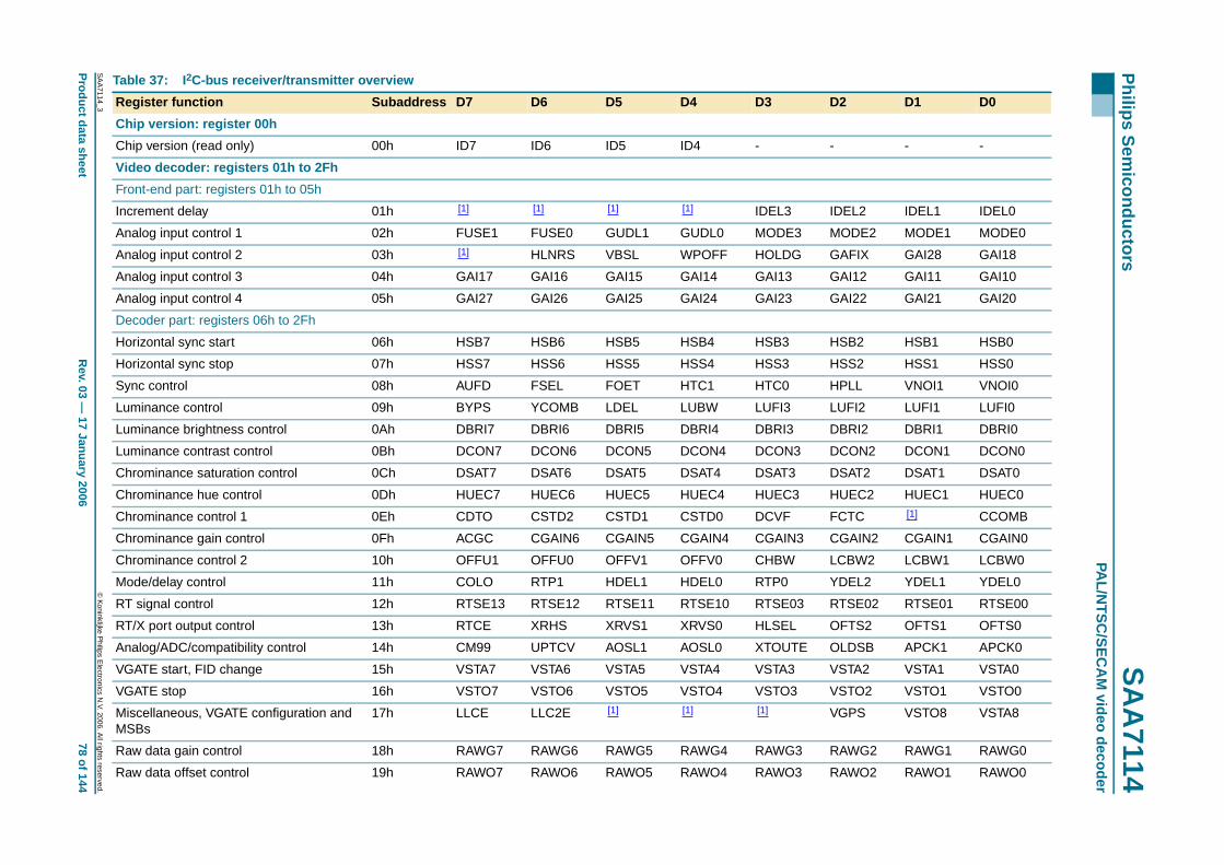
xxxxxxxxxxxxxxxxxxxxx xxxxxxxxxxxxxxxxxxxxxxxxxx xxxxxxx x x x xxxxxxxxxxxxxxxxxxxxxxxxxxxxxx xxxxxxxxxxxxxxxxxxx xx xxxxxxx xxxxxxxxxxxxxxxxxxxxxxxxxxx xxxxxxxxxxxxxxxxxxx xxxxxx xxxxxxxxxxxxxxxxxxxxxxxxxxxxxxxxxxx xxxxxxxxxxxx x xxxxxxxxxxxxxxxxxxxxxx xxxxxxxxxxxxxxxxxxxxxxxxxxxxxx xxxxx xxxxxxxxxxxxxxxxxxxxxxxxxxxxxxxxxxxxxxxxxxxxxxxxxx xxxxxxxxxxxxxxxxxxxxxxxxxxxxxxxxx xxxxxxxxxxxxxxxxxxxx xxx
SA
A7114_3
Product data shee
Philips S
emiconductors
SA
A7114
PAL/N
TS
C/S
EC
AM
video decoder
Table 37: I 2C-bus receiver/transmitter overview
Register function Subaddress D7 D6 D5 D4 D3 D2 D1 D0
Chip version: register 00h
Chip version (read only) 00h ID7 ID6 ID5 ID4 - - - -
IDEL2 IDEL1 IDEL0
MODE2 MODE1 MODE0
GAFIX GAI28 GAI18
GAI12 GAI11 GAI10
GAI22 GAI21 GAI20
HSB2 HSB1 HSB0
HSS2 HSS1 HSS0
HPLL VNOI1 VNOI0
LUFI2 LUFI1 LUFI0
DBRI2 DBRI1 DBRI0
DCON2 DCON1 DCON0
DSAT2 DSAT1 DSAT0
HUEC2 HUEC1 HUEC0
FCTC [1] CCOMB
CGAIN2 CGAIN1 CGAIN0
LCBW2 LCBW1 LCBW0
YDEL2 YDEL1 YDEL0
RTSE02 RTSE01 RTSE00
OFTS2 OFTS1 OFTS0
OLDSB APCK1 APCK0
VSTA2 VSTA1 VSTA0
VSTO2 VSTO1 VSTO0
VGPS VSTO8 VSTA8
RAWG2 RAWG1 RAWG0
RAWO2 RAWO1 RAWO0
© K
oninklijke Philips E
lectronics N.V. 2006. A
ll rights reserved.
tR
ev. 03 — 17 January 2006
78 of 144
Video decoder: registers 01h to 2Fh
Front-end part: registers 01h to 05h
Increment delay 01h [1] [1] [1] [1] IDEL3
Analog input control 1 02h FUSE1 FUSE0 GUDL1 GUDL0 MODE3
Analog input control 2 03h [1] HLNRS VBSL WPOFF HOLDG
Analog input control 3 04h GAI17 GAI16 GAI15 GAI14 GAI13
Analog input control 4 05h GAI27 GAI26 GAI25 GAI24 GAI23
Decoder part: registers 06h to 2Fh
Horizontal sync start 06h HSB7 HSB6 HSB5 HSB4 HSB3
Horizontal sync stop 07h HSS7 HSS6 HSS5 HSS4 HSS3
Sync control 08h AUFD FSEL FOET HTC1 HTC0
Luminance control 09h BYPS YCOMB LDEL LUBW LUFI3
Luminance brightness control 0Ah DBRI7 DBRI6 DBRI5 DBRI4 DBRI3
Luminance contrast control 0Bh DCON7 DCON6 DCON5 DCON4 DCON3
Chrominance saturation control 0Ch DSAT7 DSAT6 DSAT5 DSAT4 DSAT3
Chrominance hue control 0Dh HUEC7 HUEC6 HUEC5 HUEC4 HUEC3
Chrominance control 1 0Eh CDTO CSTD2 CSTD1 CSTD0 DCVF
Chrominance gain control 0Fh ACGC CGAIN6 CGAIN5 CGAIN4 CGAIN3
Chrominance control 2 10h OFFU1 OFFU0 OFFV1 OFFV0 CHBW
Mode/delay control 11h COLO RTP1 HDEL1 HDEL0 RTP0
RT signal control 12h RTSE13 RTSE12 RTSE11 RTSE10 RTSE03
RT/X port output control 13h RTCE XRHS XRVS1 XRVS0 HLSEL
Analog/ADC/compatibility control 14h CM99 UPTCV AOSL1 AOSL0 XTOUTE
VGATE start, FID change 15h VSTA7 VSTA6 VSTA5 VSTA4 VSTA3
VGATE stop 16h VSTO7 VSTO6 VSTO5 VSTO4 VSTO3
Miscellaneous, VGATE configuration andMSBs
17h LLCE LLC2E [1] [1] [1]
Raw data gain control 18h RAWG7 RAWG6 RAWG5 RAWG4 RAWG3
Raw data offset control 19h RAWO7 RAWO6 RAWO5 RAWO4 RAWO3
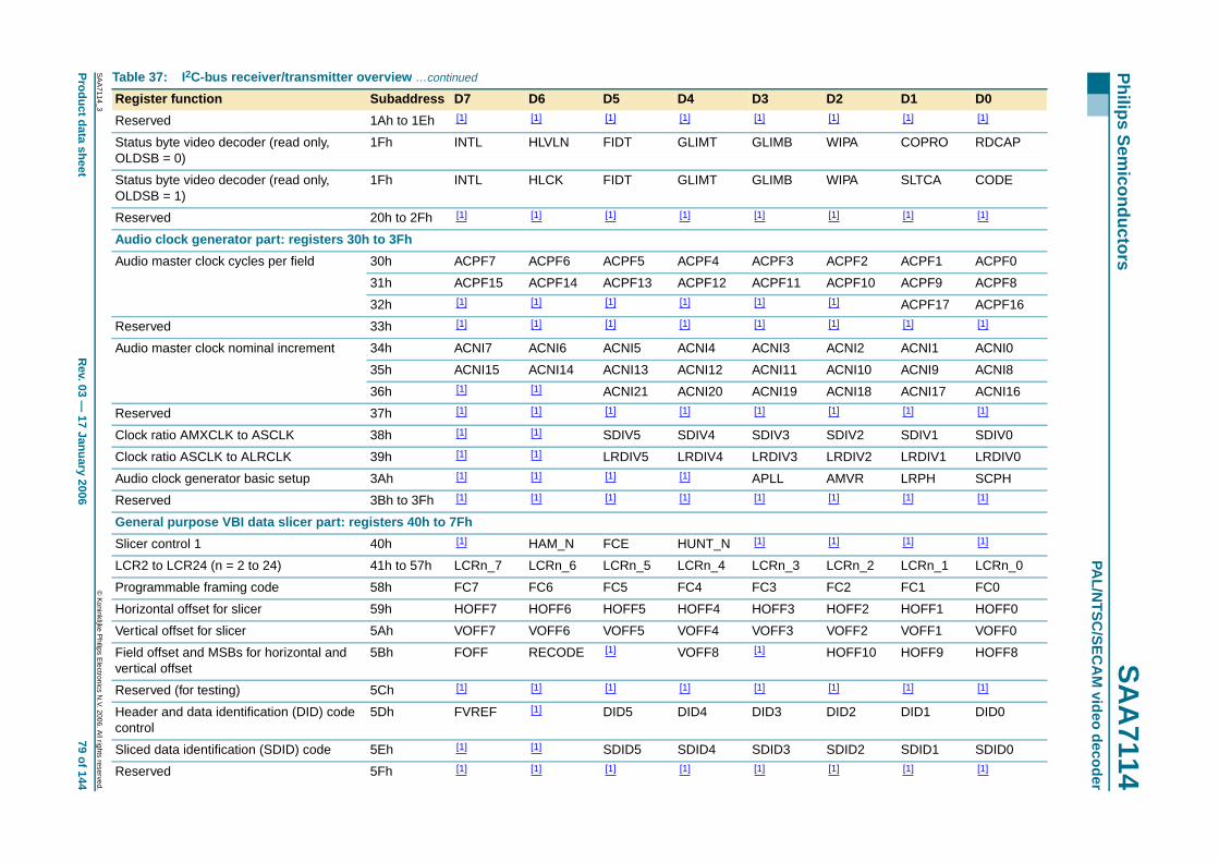
xxxxxxxxxxxxxxxxxxxxx xxxxxxxxxxxxxxxxxxxxxxxxxx xxxxxxx x x x xxxxxxxxxxxxxxxxxxxxxxxxxxxxxx xxxxxxxxxxxxxxxxxxx xx xxxxxxx xxxxxxxxxxxxxxxxxxxxxxxxxxx xxxxxxxxxxxxxxxxxxx xxxxxx xxxxxxxxxxxxxxxxxxxxxxxxxxxxxxxxxxx xxxxxxxxxxxx x xxxxxxxxxxxxxxxxxxxxxx xxxxxxxxxxxxxxxxxxxxxxxxxxxxxx xxxxx xxxxxxxxxxxxxxxxxxxxxxxxxxxxxxxxxxxxxxxxxxxxxxxxxx xxxxxxxxxxxxxxxxxxxxxxxxxxxxxxxxx xxxxxxxxxxxxxxxxxxxx xxx
SA
A7114_3
Product data shee
Philips S
emiconductors
SA
A7114
PAL/N
TS
C/S
EC
AM
video decoderReserved 1Ah to 1Eh [1] [1] [1] [1] [1] [1] [1] [1]
Status byte video decoder (read only, 1Fh INTL HLVLN FIDT GLIMT GLIMB WIPA COPRO RDCAP
WIPA SLTCA CODE
[1] [1] [1]
ACPF2 ACPF1 ACPF0
ACPF10 ACPF9 ACPF8[1] ACPF17 ACPF16[1] [1] [1]
ACNI2 ACNI1 ACNI0
ACNI10 ACNI9 ACNI8
ACNI18 ACNI17 ACNI16[1] [1] [1]
SDIV2 SDIV1 SDIV0
LRDIV2 LRDIV1 LRDIV0
AMVR LRPH SCPH[1] [1] [1]
[1] [1] [1]
LCRn_2 LCRn_1 LCRn_0
FC2 FC1 FC0
HOFF2 HOFF1 HOFF0
VOFF2 VOFF1 VOFF0
HOFF10 HOFF9 HOFF8
[1] [1] [1]
DID2 DID1 DID0
SDID2 SDID1 SDID0[1] [1] [1]
Table 37: I 2C-bus receiver/transmitter overview …continued
Register function Subaddress D7 D6 D5 D4 D3 D2 D1 D0
© K
oninklijke Philips E
lectronics N.V. 2006. A
ll rights reserved.
tR
ev. 03 — 17 January 2006
79 of 144
OLDSB = 0)
Status byte video decoder (read only,OLDSB = 1)
1Fh INTL HLCK FIDT GLIMT GLIMB
Reserved 20h to 2Fh [1] [1] [1] [1] [1]
Audio clock generator part: registers 30h to 3Fh
Audio master clock cycles per field 30h ACPF7 ACPF6 ACPF5 ACPF4 ACPF3
31h ACPF15 ACPF14 ACPF13 ACPF12 ACPF11
32h [1] [1] [1] [1] [1]
Reserved 33h [1] [1] [1] [1] [1]
Audio master clock nominal increment 34h ACNI7 ACNI6 ACNI5 ACNI4 ACNI3
35h ACNI15 ACNI14 ACNI13 ACNI12 ACNI11
36h [1] [1] ACNI21 ACNI20 ACNI19
Reserved 37h [1] [1] [1] [1] [1]
Clock ratio AMXCLK to ASCLK 38h [1] [1] SDIV5 SDIV4 SDIV3
Clock ratio ASCLK to ALRCLK 39h [1] [1] LRDIV5 LRDIV4 LRDIV3
Audio clock generator basic setup 3Ah [1] [1] [1] [1] APLL
Reserved 3Bh to 3Fh [1] [1] [1] [1] [1]
General purpose VBI data slicer part: registers 40h to 7Fh
Slicer control 1 40h [1] HAM_N FCE HUNT_N [1]
LCR2 to LCR24 (n = 2 to 24) 41h to 57h LCRn_7 LCRn_6 LCRn_5 LCRn_4 LCRn_3
Programmable framing code 58h FC7 FC6 FC5 FC4 FC3
Horizontal offset for slicer 59h HOFF7 HOFF6 HOFF5 HOFF4 HOFF3
Vertical offset for slicer 5Ah VOFF7 VOFF6 VOFF5 VOFF4 VOFF3
Field offset and MSBs for horizontal andvertical offset
5Bh FOFF RECODE [1] VOFF8 [1]
Reserved (for testing) 5Ch [1] [1] [1] [1] [1]
Header and data identification (DID) codecontrol
5Dh FVREF [1] DID5 DID4 DID3
Sliced data identification (SDID) code 5Eh [1] [1] SDID5 SDID4 SDID3
Reserved 5Fh [1] [1] [1] [1] [1]
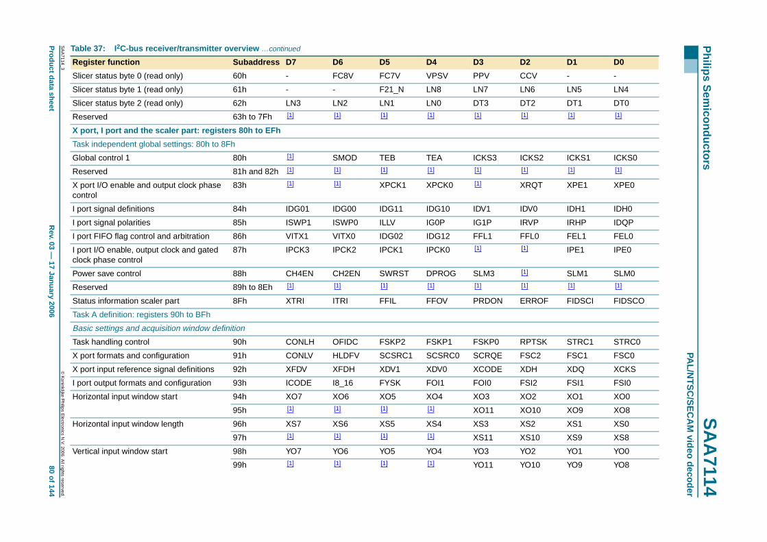
xxxxxxxxxxxxxxxxxxxxx xxxxxxxxxxxxxxxxxxxxxxxxxx xxxxxxx x x x xxxxxxxxxxxxxxxxxxxxxxxxxxxxxx xxxxxxxxxxxxxxxxxxx xx xxxxxxx xxxxxxxxxxxxxxxxxxxxxxxxxxx xxxxxxxxxxxxxxxxxxx xxxxxx xxxxxxxxxxxxxxxxxxxxxxxxxxxxxxxxxxx xxxxxxxxxxxx x xxxxxxxxxxxxxxxxxxxxxx xxxxxxxxxxxxxxxxxxxxxxxxxxxxxx xxxxx xxxxxxxxxxxxxxxxxxxxxxxxxxxxxxxxxxxxxxxxxxxxxxxxxx xxxxxxxxxxxxxxxxxxxxxxxxxxxxxxxxx xxxxxxxxxxxxxxxxxxxx xxx
SA
A7114_3
Product data shee
Philips S
emiconductors
SA
A7114
PAL/N
TS
C/S
EC
AM
video decoderSlicer status byte 0 (read only) 60h - FC8V FC7V VPSV PPV CCV - -
Slicer status byte 1 (read only) 61h - - F21_N LN8 LN7 LN6 LN5 LN4
DT2 DT1 DT0[1] [1] [1]
ICKS2 ICKS1 ICKS0[1] [1] [1]
XRQT XPE1 XPE0
IDV0 IDH1 IDH0
IRVP IRHP IDQP
FFL0 FEL1 FEL0[1] IPE1 IPE0
[1] SLM1 SLM0[1] [1] [1]
ERROF FIDSCI FIDSCO
RPTSK STRC1 STRC0
FSC2 FSC1 FSC0
XDH XDQ XCKS
FSI2 FSI1 FSI0
XO2 XO1 XO0
XO10 XO9 XO8
XS2 XS1 XS0
XS10 XS9 XS8
YO2 YO1 YO0
YO10 YO9 YO8
Table 37: I 2C-bus receiver/transmitter overview …continued
Register function Subaddress D7 D6 D5 D4 D3 D2 D1 D0
© K
oninklijke Philips E
lectronics N.V. 2006. A
ll rights reserved.
tR
ev. 03 — 17 January 2006
80 of 144
Slicer status byte 2 (read only) 62h LN3 LN2 LN1 LN0 DT3
Reserved 63h to 7Fh [1] [1] [1] [1] [1]
X port, I port and the scaler part: registers 80h to EFh
Task independent global settings: 80h to 8Fh
Global control 1 80h [1] SMOD TEB TEA ICKS3
Reserved 81h and 82h [1] [1] [1] [1] [1]
X port I/O enable and output clock phasecontrol
83h [1] [1] XPCK1 XPCK0 [1]
I port signal definitions 84h IDG01 IDG00 IDG11 IDG10 IDV1
I port signal polarities 85h ISWP1 ISWP0 ILLV IG0P IG1P
I port FIFO flag control and arbitration 86h VITX1 VITX0 IDG02 IDG12 FFL1
I port I/O enable, output clock and gatedclock phase control
87h IPCK3 IPCK2 IPCK1 IPCK0 [1]
Power save control 88h CH4EN CH2EN SWRST DPROG SLM3
Reserved 89h to 8Eh [1] [1] [1] [1] [1]
Status information scaler part 8Fh XTRI ITRI FFIL FFOV PRDON
Task A definition: registers 90h to BFh
Basic settings and acquisition window definition
Task handling control 90h CONLH OFIDC FSKP2 FSKP1 FSKP0
X port formats and configuration 91h CONLV HLDFV SCSRC1 SCSRC0 SCRQE
X port input reference signal definitions 92h XFDV XFDH XDV1 XDV0 XCODE
I port output formats and configuration 93h ICODE I8_16 FYSK FOI1 FOI0
Horizontal input window start 94h XO7 XO6 XO5 XO4 XO3
95h [1] [1] [1] [1] XO11
Horizontal input window length 96h XS7 XS6 XS5 XS4 XS3
97h [1] [1] [1] [1] XS11
Vertical input window start 98h YO7 YO6 YO5 YO4 YO3
99h [1] [1] [1] [1] YO11
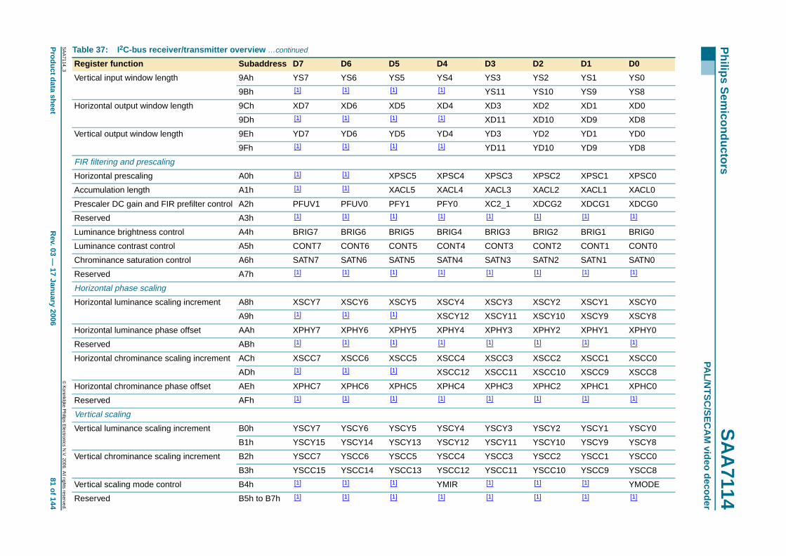
xxxxxxxxxxxxxxxxxxxxx xxxxxxxxxxxxxxxxxxxxxxxxxx xxxxxxx x x x xxxxxxxxxxxxxxxxxxxxxxxxxxxxxx xxxxxxxxxxxxxxxxxxx xx xxxxxxx xxxxxxxxxxxxxxxxxxxxxxxxxxx xxxxxxxxxxxxxxxxxxx xxxxxx xxxxxxxxxxxxxxxxxxxxxxxxxxxxxxxxxxx xxxxxxxxxxxx x xxxxxxxxxxxxxxxxxxxxxx xxxxxxxxxxxxxxxxxxxxxxxxxxxxxx xxxxx xxxxxxxxxxxxxxxxxxxxxxxxxxxxxxxxxxxxxxxxxxxxxxxxxx xxxxxxxxxxxxxxxxxxxxxxxxxxxxxxxxx xxxxxxxxxxxxxxxxxxxx xxx
SA
A7114_3
Product data shee
Philips S
emiconductors
SA
A7114
PAL/N
TS
C/S
EC
AM
video decoderVertical input window length 9Ah YS7 YS6 YS5 YS4 YS3 YS2 YS1 YS0
9Bh [1] [1] [1] [1] YS11 YS10 YS9 YS8
XD2 XD1 XD0
XD10 XD9 XD8
YD2 YD1 YD0
YD10 YD9 YD8
XPSC2 XPSC1 XPSC0
XACL2 XACL1 XACL0
XDCG2 XDCG1 XDCG0[1] [1] [1]
BRIG2 BRIG1 BRIG0
CONT2 CONT1 CONT0
SATN2 SATN1 SATN0[1] [1] [1]
XSCY2 XSCY1 XSCY0
XSCY10 XSCY9 XSCY8
XPHY2 XPHY1 XPHY0[1] [1] [1]
XSCC2 XSCC1 XSCC0
XSCC10 XSCC9 XSCC8
XPHC2 XPHC1 XPHC0[1] [1] [1]
YSCY2 YSCY1 YSCY0
YSCY10 YSCY9 YSCY8
YSCC2 YSCC1 YSCC0
YSCC10 YSCC9 YSCC8[1] [1] YMODE[1] [1] [1]
Table 37: I 2C-bus receiver/transmitter overview …continued
Register function Subaddress D7 D6 D5 D4 D3 D2 D1 D0
© K
oninklijke Philips E
lectronics N.V. 2006. A
ll rights reserved.
tR
ev. 03 — 17 January 2006
81 of 144
Horizontal output window length 9Ch XD7 XD6 XD5 XD4 XD3
9Dh [1] [1] [1] [1] XD11
Vertical output window length 9Eh YD7 YD6 YD5 YD4 YD3
9Fh [1] [1] [1] [1] YD11
FIR filtering and prescaling
Horizontal prescaling A0h [1] [1] XPSC5 XPSC4 XPSC3
Accumulation length A1h [1] [1] XACL5 XACL4 XACL3
Prescaler DC gain and FIR prefilter control A2h PFUV1 PFUV0 PFY1 PFY0 XC2_1
Reserved A3h [1] [1] [1] [1] [1]
Luminance brightness control A4h BRIG7 BRIG6 BRIG5 BRIG4 BRIG3
Luminance contrast control A5h CONT7 CONT6 CONT5 CONT4 CONT3
Chrominance saturation control A6h SATN7 SATN6 SATN5 SATN4 SATN3
Reserved A7h [1] [1] [1] [1] [1]
Horizontal phase scaling
Horizontal luminance scaling increment A8h XSCY7 XSCY6 XSCY5 XSCY4 XSCY3
A9h [1] [1] [1] XSCY12 XSCY11
Horizontal luminance phase offset AAh XPHY7 XPHY6 XPHY5 XPHY4 XPHY3
Reserved ABh [1] [1] [1] [1] [1]
Horizontal chrominance scaling increment ACh XSCC7 XSCC6 XSCC5 XSCC4 XSCC3
ADh [1] [1] [1] XSCC12 XSCC11
Horizontal chrominance phase offset AEh XPHC7 XPHC6 XPHC5 XPHC4 XPHC3
Reserved AFh [1] [1] [1] [1] [1]
Vertical scaling
Vertical luminance scaling increment B0h YSCY7 YSCY6 YSCY5 YSCY4 YSCY3
B1h YSCY15 YSCY14 YSCY13 YSCY12 YSCY11
Vertical chrominance scaling increment B2h YSCC7 YSCC6 YSCC5 YSCC4 YSCC3
B3h YSCC15 YSCC14 YSCC13 YSCC12 YSCC11
Vertical scaling mode control B4h [1] [1] [1] YMIR [1]
Reserved B5h to B7h [1] [1] [1] [1] [1]
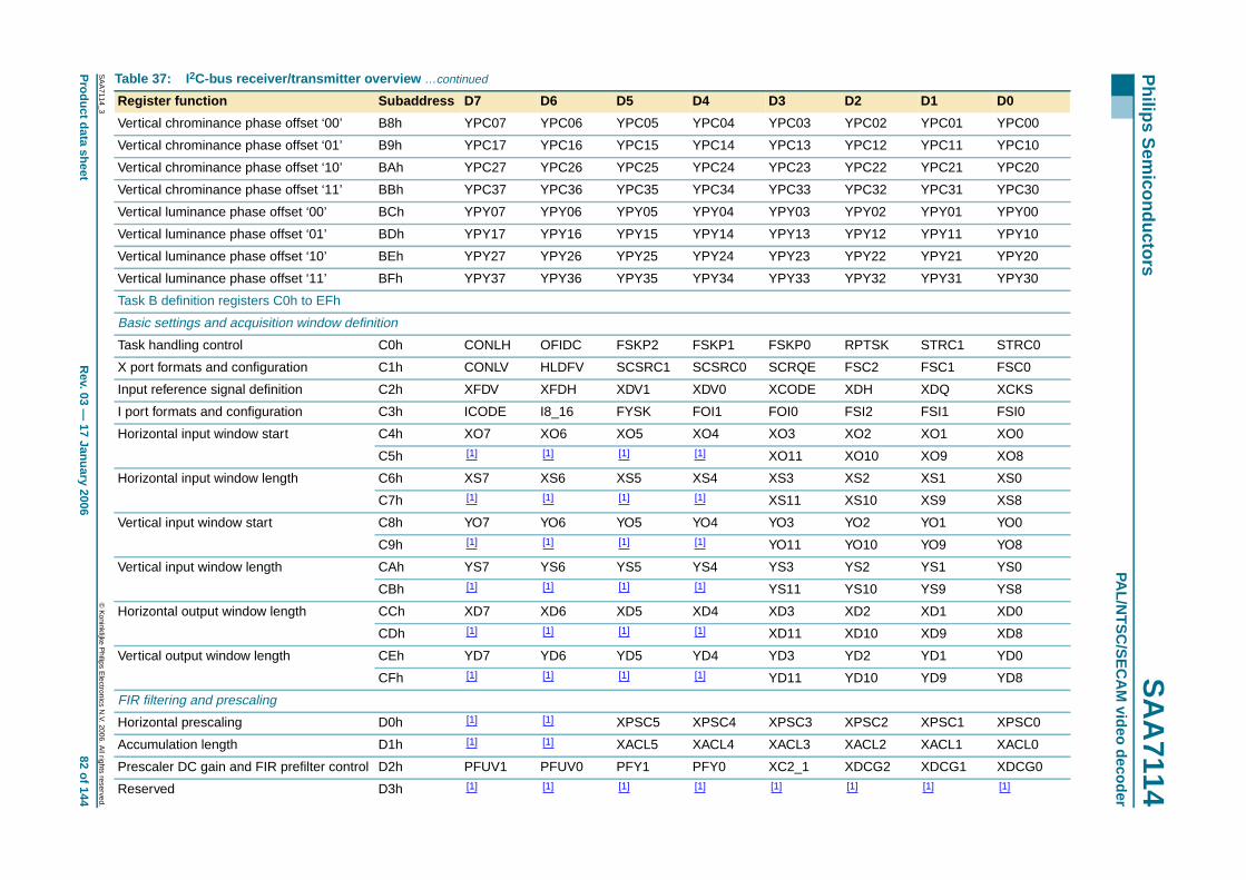
xxxxxxxxxxxxxxxxxxxxx xxxxxxxxxxxxxxxxxxxxxxxxxx xxxxxxx x x x xxxxxxxxxxxxxxxxxxxxxxxxxxxxxx xxxxxxxxxxxxxxxxxxx xx xxxxxxx xxxxxxxxxxxxxxxxxxxxxxxxxxx xxxxxxxxxxxxxxxxxxx xxxxxx xxxxxxxxxxxxxxxxxxxxxxxxxxxxxxxxxxx xxxxxxxxxxxx x xxxxxxxxxxxxxxxxxxxxxx xxxxxxxxxxxxxxxxxxxxxxxxxxxxxx xxxxx xxxxxxxxxxxxxxxxxxxxxxxxxxxxxxxxxxxxxxxxxxxxxxxxxx xxxxxxxxxxxxxxxxxxxxxxxxxxxxxxxxx xxxxxxxxxxxxxxxxxxxx xxx
SA
A7114_3
Product data shee
Philips S
emiconductors
SA
A7114
PAL/N
TS
C/S
EC
AM
video decoderVertical chrominance phase offset ‘00’ B8h YPC07 YPC06 YPC05 YPC04 YPC03 YPC02 YPC01 YPC00
Vertical chrominance phase offset ‘01’ B9h YPC17 YPC16 YPC15 YPC14 YPC13 YPC12 YPC11 YPC10
YPC22 YPC21 YPC20
YPC32 YPC31 YPC30
YPY02 YPY01 YPY00
YPY12 YPY11 YPY10
YPY22 YPY21 YPY20
YPY32 YPY31 YPY30
RPTSK STRC1 STRC0
FSC2 FSC1 FSC0
XDH XDQ XCKS
FSI2 FSI1 FSI0
XO2 XO1 XO0
XO10 XO9 XO8
XS2 XS1 XS0
XS10 XS9 XS8
YO2 YO1 YO0
YO10 YO9 YO8
YS2 YS1 YS0
YS10 YS9 YS8
XD2 XD1 XD0
XD10 XD9 XD8
YD2 YD1 YD0
YD10 YD9 YD8
XPSC2 XPSC1 XPSC0
XACL2 XACL1 XACL0
XDCG2 XDCG1 XDCG0[1] [1] [1]
Table 37: I 2C-bus receiver/transmitter overview …continued
Register function Subaddress D7 D6 D5 D4 D3 D2 D1 D0
© K
oninklijke Philips E
lectronics N.V. 2006. A
ll rights reserved.
tR
ev. 03 — 17 January 2006
82 of 144
Vertical chrominance phase offset ‘10’ BAh YPC27 YPC26 YPC25 YPC24 YPC23
Vertical chrominance phase offset ‘11’ BBh YPC37 YPC36 YPC35 YPC34 YPC33
Vertical luminance phase offset ‘00’ BCh YPY07 YPY06 YPY05 YPY04 YPY03
Vertical luminance phase offset ‘01’ BDh YPY17 YPY16 YPY15 YPY14 YPY13
Vertical luminance phase offset ‘10’ BEh YPY27 YPY26 YPY25 YPY24 YPY23
Vertical luminance phase offset ‘11’ BFh YPY37 YPY36 YPY35 YPY34 YPY33
Task B definition registers C0h to EFh
Basic settings and acquisition window definition
Task handling control C0h CONLH OFIDC FSKP2 FSKP1 FSKP0
X port formats and configuration C1h CONLV HLDFV SCSRC1 SCSRC0 SCRQE
Input reference signal definition C2h XFDV XFDH XDV1 XDV0 XCODE
I port formats and configuration C3h ICODE I8_16 FYSK FOI1 FOI0
Horizontal input window start C4h XO7 XO6 XO5 XO4 XO3
C5h [1] [1] [1] [1] XO11
Horizontal input window length C6h XS7 XS6 XS5 XS4 XS3
C7h [1] [1] [1] [1] XS11
Vertical input window start C8h YO7 YO6 YO5 YO4 YO3
C9h [1] [1] [1] [1] YO11
Vertical input window length CAh YS7 YS6 YS5 YS4 YS3
CBh [1] [1] [1] [1] YS11
Horizontal output window length CCh XD7 XD6 XD5 XD4 XD3
CDh [1] [1] [1] [1] XD11
Vertical output window length CEh YD7 YD6 YD5 YD4 YD3
CFh [1] [1] [1] [1] YD11
FIR filtering and prescaling
Horizontal prescaling D0h [1] [1] XPSC5 XPSC4 XPSC3
Accumulation length D1h [1] [1] XACL5 XACL4 XACL3
Prescaler DC gain and FIR prefilter control D2h PFUV1 PFUV0 PFY1 PFY0 XC2_1
Reserved D3h [1] [1] [1] [1] [1]
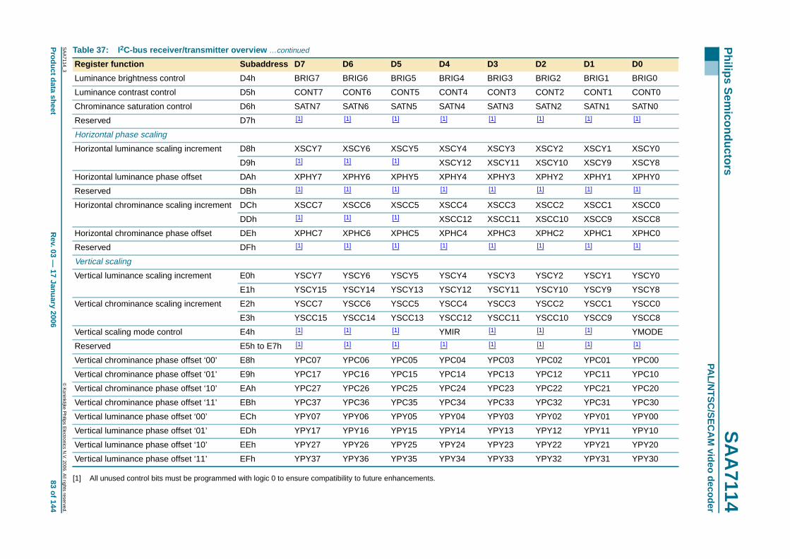
xxxxxxxxxxxxxxxxxxxxx xxxxxxxxxxxxxxxxxxxxxxxxxx xxxxxxx x x x xxxxxxxxxxxxxxxxxxxxxxxxxxxxxx xxxxxxxxxxxxxxxxxxx xx xxxxxxx xxxxxxxxxxxxxxxxxxxxxxxxxxx xxxxxxxxxxxxxxxxxxx xxxxxx xxxxxxxxxxxxxxxxxxxxxxxxxxxxxxxxxxx xxxxxxxxxxxx x xxxxxxxxxxxxxxxxxxxxxx xxxxxxxxxxxxxxxxxxxxxxxxxxxxxx xxxxx xxxxxxxxxxxxxxxxxxxxxxxxxxxxxxxxxxxxxxxxxxxxxxxxxx xxxxxxxxxxxxxxxxxxxxxxxxxxxxxxxxx xxxxxxxxxxxxxxxxxxxx xxx
SA
A7114_3
Product data shee
Philips S
emiconductors
SA
A7114
PAL/N
TS
C/S
EC
AM
video decoderLuminance brightness control D4h BRIG7 BRIG6 BRIG5 BRIG4 BRIG3 BRIG2 BRIG1 BRIG0
Luminance contrast control D5h CONT7 CONT6 CONT5 CONT4 CONT3 CONT2 CONT1 CONT0
SATN2 SATN1 SATN0[1] [1] [1]
XSCY2 XSCY1 XSCY0
XSCY10 XSCY9 XSCY8
XPHY2 XPHY1 XPHY0[1] [1] [1]
XSCC2 XSCC1 XSCC0
XSCC10 XSCC9 XSCC8
XPHC2 XPHC1 XPHC0[1] [1] [1]
YSCY2 YSCY1 YSCY0
YSCY10 YSCY9 YSCY8
YSCC2 YSCC1 YSCC0
YSCC10 YSCC9 YSCC8[1] [1] YMODE[1] [1] [1]
YPC02 YPC01 YPC00
YPC12 YPC11 YPC10
YPC22 YPC21 YPC20
YPC32 YPC31 YPC30
YPY02 YPY01 YPY00
YPY12 YPY11 YPY10
YPY22 YPY21 YPY20
YPY32 YPY31 YPY30
Table 37: I 2C-bus receiver/transmitter overview …continued
Register function Subaddress D7 D6 D5 D4 D3 D2 D1 D0
© K
oninklijke Philips E
lectronics N.V. 2006. A
ll rights reserved.
tR
ev. 03 — 17 January 2006
83 of 144
[1] All unused control bits must be programmed with logic 0 to ensure compatibility to future enhancements.
Chrominance saturation control D6h SATN7 SATN6 SATN5 SATN4 SATN3
Reserved D7h [1] [1] [1] [1] [1]
Horizontal phase scaling
Horizontal luminance scaling increment D8h XSCY7 XSCY6 XSCY5 XSCY4 XSCY3
D9h [1] [1] [1] XSCY12 XSCY11
Horizontal luminance phase offset DAh XPHY7 XPHY6 XPHY5 XPHY4 XPHY3
Reserved DBh [1] [1] [1] [1] [1]
Horizontal chrominance scaling increment DCh XSCC7 XSCC6 XSCC5 XSCC4 XSCC3
DDh [1] [1] [1] XSCC12 XSCC11
Horizontal chrominance phase offset DEh XPHC7 XPHC6 XPHC5 XPHC4 XPHC3
Reserved DFh [1] [1] [1] [1] [1]
Vertical scaling
Vertical luminance scaling increment E0h YSCY7 YSCY6 YSCY5 YSCY4 YSCY3
E1h YSCY15 YSCY14 YSCY13 YSCY12 YSCY11
Vertical chrominance scaling increment E2h YSCC7 YSCC6 YSCC5 YSCC4 YSCC3
E3h YSCC15 YSCC14 YSCC13 YSCC12 YSCC11
Vertical scaling mode control E4h [1] [1] [1] YMIR [1]
Reserved E5h to E7h [1] [1] [1] [1] [1]
Vertical chrominance phase offset ‘00’ E8h YPC07 YPC06 YPC05 YPC04 YPC03
Vertical chrominance phase offset ‘01’ E9h YPC17 YPC16 YPC15 YPC14 YPC13
Vertical chrominance phase offset ‘10’ EAh YPC27 YPC26 YPC25 YPC24 YPC23
Vertical chrominance phase offset ‘11’ EBh YPC37 YPC36 YPC35 YPC34 YPC33
Vertical luminance phase offset ‘00’ ECh YPY07 YPY06 YPY05 YPY04 YPY03
Vertical luminance phase offset ‘01’ EDh YPY17 YPY16 YPY15 YPY14 YPY13
Vertical luminance phase offset ‘10’ EEh YPY27 YPY26 YPY25 YPY24 YPY23
Vertical luminance phase offset ‘11’ EFh YPY37 YPY36 YPY35 YPY34 YPY33
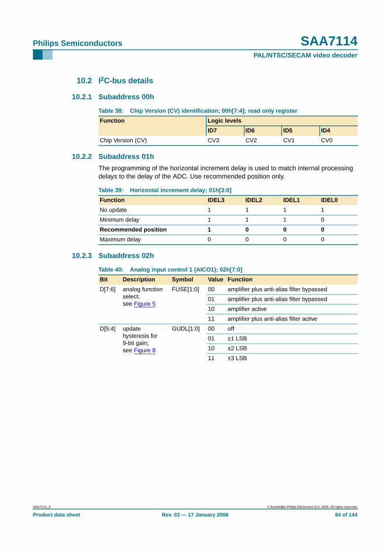
Philips Semiconductors SAA7114PAL/NTSC/SECAM video decoder
10.2 I2C-bus details
10.2.1 Subaddress 00h
10.2.2 Subaddress 01h
The programming of the horizontal increment delay is used to match internal processingdelays to the delay of the ADC. Use recommended position only.
10.2.3 Subaddress 02h
Table 38: Chip Version (CV) identification; 00h[7:4]; read only register
Function Logic levels
ID7 ID6 ID5 ID4
Chip Version (CV) CV3 CV2 CV1 CV0
Table 39: Horizontal increment delay; 01h[3:0]
Function IDEL3 IDEL2 IDEL1 IDEL0
No update 1 1 1 1
Minimum delay 1 1 1 0
Recommended position 1 0 0 0
Maximum delay 0 0 0 0
Table 40: Analog input control 1 (AICO1); 02h[7:0]
Bit Description Symbol Value Function
D[7:6] analog functionselect;see Figure 5
FUSE[1:0] 00 amplifier plus anti-alias filter bypassed
01 amplifier plus anti-alias filter bypassed
10 amplifier active
11 amplifier plus anti-alias filter active
D[5:4] updatehysteresis for9-bit gain;see Figure 8
GUDL[1:0] 00 off
01 ±1 LSB
10 ±2 LSB
11 ±3 LSB
SAA7114_3 © Koninklijke Philips Electronics N.V. 2006. All rights reserved.
Product data sheet Rev. 03 — 17 January 2006 84 of 144
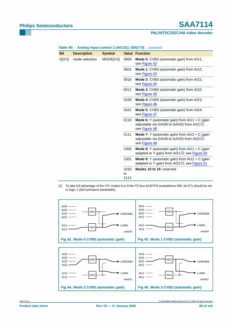
Philips Semiconductors SAA7114PAL/NTSC/SECAM video decoder
[1] To take full advantage of the Y/C modes 6 to 9 the I2C-bus bit BYPS (subaddress 09h, bit D7) should be setto logic 1 (full luminance bandwidth).
D[3:0] mode selection MODE[3:0] 0000 Mode 0 : CVBS (automatic gain) from AI11;see Figure 42
0001 Mode 1 : CVBS (automatic gain) from AI12;see Figure 43
0010 Mode 2 : CVBS (automatic gain) from AI21;see Figure 44
0011 Mode 3 : CVBS (automatic gain) from AI22;see Figure 45
0100 Mode 4 : CVBS (automatic gain) from AI23;see Figure 46
0101 Mode 5 : CVBS (automatic gain) from AI24;see Figure 47
0110 Mode 6 : Y (automatic gain) from AI11 + C (gainadjustable via GAI28 to GAI20) from AI21 [1];see Figure 48
0111 Mode 7 : Y (automatic gain) from AI12 + C (gainadjustable via GAI28 to GAI20) from AI22 [1];see Figure 49
1000 Mode 8 : Y (automatic gain) from AI11 + C (gainadapted to Y gain) from AI21 [1]; see Figure 50
1001 Mode 9 : Y (automatic gain) from AI12 + C (gainadapted to Y gain) from AI22 [1]; see Figure 51
1010to1111
Modes 10 to 15 : reserved
Fig 42. Mode 0 CVBS (automatic gain) Fig 43. Mode 1 CVBS (automatic gain)
Fig 44. Mode 2 CVBS (automatic gain) Fig 45. Mode 3 CVBS (automatic gain)
Table 40: Analog input control 1 (AICO1); 02h[7:0] …continued
Bit Description Symbol Value Function
mhb559
AI22AI21
AI12AI11
AD2
AD1
CHROMA
LUMA
AI24AI23
mhb560
AI12AI11
AD2
AD1
CHROMA
LUMA
AI22AI21
AI24AI23
mhb561
AI12AI11
AD2
AD1
CHROMA
LUMA
AI22AI21
AI24AI23
mhb562
AI12AI11
AD2
AD1
CHROMA
LUMA
AI22AI21
AI24AI23
SAA7114_3 © Koninklijke Philips Electronics N.V. 2006. All rights reserved.
Product data sheet Rev. 03 — 17 January 2006 85 of 144
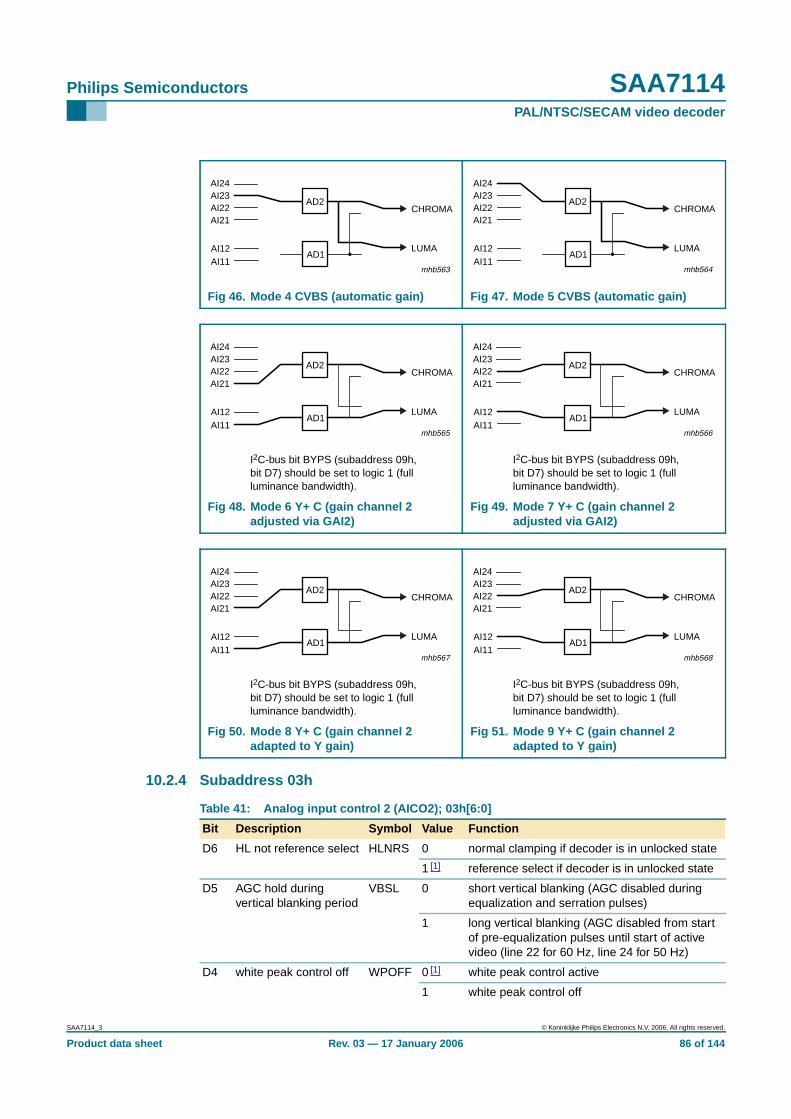
Philips Semiconductors SAA7114PAL/NTSC/SECAM video decoder
10.2.4 Subaddress 03h
Fig 46. Mode 4 CVBS (automatic gain) Fig 47. Mode 5 CVBS (automatic gain)
I2C-bus bit BYPS (subaddress 09h,bit D7) should be set to logic 1 (fullluminance bandwidth).
I2C-bus bit BYPS (subaddress 09h,bit D7) should be set to logic 1 (fullluminance bandwidth).
Fig 48. Mode 6 Y+ C (gain channel 2adjusted via GAI2)
Fig 49. Mode 7 Y+ C (gain channel 2adjusted via GAI2)
I2C-bus bit BYPS (subaddress 09h,bit D7) should be set to logic 1 (fullluminance bandwidth).
I2C-bus bit BYPS (subaddress 09h,bit D7) should be set to logic 1 (fullluminance bandwidth).
Fig 50. Mode 8 Y+ C (gain channel 2adapted to Y gain)
Fig 51. Mode 9 Y+ C (gain channel 2adapted to Y gain)
mhb563
AI12AI11
AD2
AD1
CHROMA
LUMA
AI22AI21
AI24AI23
mhb564
AI12AI11
AD2
AD1
CHROMA
LUMA
AI22AI21
AI24AI23
mhb565
AI12AI11
AD2
AD1
CHROMA
LUMA
AI22AI21
AI24AI23
mhb566
AI12AI11
AD2
AD1
CHROMA
LUMA
AI22AI21
AI24AI23
mhb567
AI12AI11
AD2
AD1
CHROMA
LUMA
AI22AI21
AI24AI23
mhb568
AI12AI11
AD2
AD1
CHROMA
LUMA
AI22AI21
AI24AI23
Table 41: Analog input control 2 (AICO2); 03h[6:0]
Bit Description Symbol Value Function
D6 HL not reference select HLNRS 0 normal clamping if decoder is in unlocked state
1 [1] reference select if decoder is in unlocked state
D5 AGC hold duringvertical blanking period
VBSL 0 short vertical blanking (AGC disabled duringequalization and serration pulses)
1 long vertical blanking (AGC disabled from startof pre-equalization pulses until start of activevideo (line 22 for 60 Hz, line 24 for 50 Hz)
D4 white peak control off WPOFF 0 [1] white peak control active
1 white peak control off
SAA7114_3 © Koninklijke Philips Electronics N.V. 2006. All rights reserved.
Product data sheet Rev. 03 — 17 January 2006 86 of 144
Philips Semiconductors SAA7114PAL/NTSC/SECAM video decoder
[1] HLNRS = 1 should not be used in combination with WPOFF = 0.
10.2.5 Subaddress 04h
10.2.6 Subaddress 05h
10.2.7 Subaddress 06h
D3 automatic gain controlintegration
HOLDG 0 AGC active
1 AGC integration hold (freeze)
D2 gain control fix GAFIX 0 automatic gain controlled byMODE3 to MODE0
1 gain is user programmable via GAI[17:10] andGAI[27:20]
D1 static gain controlchannel 2 sign bit
GAI28 see Table 43
D0 static gain controlchannel 1 sign bit
GAI18 see Table 42
Table 41: Analog input control 2 (AICO2); 03h[6:0] …continued
Bit Description Symbol Value Function
Table 42: Analog input control 3 (AICO3): static gain control channel 1; 03h[0] and 04h[7:0]
Decimalvalue
Gain(dB)
Sign bit03h[0]
Control bits D7 to D0
GAI18 GAI17 GAI16 GAI15 GAI14 GAI13 GAI12 GAI11 GAI10
0... −3 0 0 0 0 0 0 0 0 0
...144 0 0 1 0 0 1 0 0 0 0
145... 0 0 1 0 0 1 0 0 0 1
...511 +6 1 1 1 1 1 1 1 1 1
Table 43: Analog input control 4 (AICO4); static gain control channel 2; 03h[1] and 05h[7:0]
Decimalvalue
Gain(dB)
Sign bit03h[1]
Control bits D7 to D0
GAI28 GAI27 GAI26 GAI25 GAI24 GAI23 GAI22 GAI21 GAI20
0... −3 0 0 0 0 0 0 0 0 0
...144 0 0 1 0 0 1 0 0 0 0
145... 0 0 1 0 0 1 0 0 0 1
...511 +6 1 1 1 1 1 1 1 1 1
Table 44: Horizontal sync start; 06h[7:0]
Delay time (stepsize = 8/LLC)
Control bits D7 to D0
HSB7 HSB6 HSB5 HSB4 HSB3 HSB2 HSB1 HSB0
−128...−109 (50 Hz) forbidden (outside available central counter range)
−128...−108 (60 Hz) forbidden (outside available central counter range)
−108 (50 Hz)... 1 0 0 1 0 1 0 0
−107 (60 Hz)... 1 0 0 1 0 1 0 1
...108 (50 Hz) 0 1 1 0 1 1 0 0
SAA7114_3 © Koninklijke Philips Electronics N.V. 2006. All rights reserved.
Product data sheet Rev. 03 — 17 January 2006 87 of 144
Philips Semiconductors SAA7114PAL/NTSC/SECAM video decoder
10.2.8 Subaddress 07h
10.2.9 Subaddress 08h
...107 (60 Hz) 0 1 1 0 1 0 1 1
109...127 (50 Hz) forbidden (outside available central counter range)
108...127 (60 Hz) forbidden (outside available central counter range)
Table 44: Horizontal sync start; 06h[7:0] …continued
Delay time (stepsize = 8/LLC)
Control bits D7 to D0
HSB7 HSB6 HSB5 HSB4 HSB3 HSB2 HSB1 HSB0
Table 45: Horizontal sync stop; 07h[7:0]
Delay time (stepsize = 8/LLC)
Control bits D7 to D0
HSS7 HSS6 HSS5 HSS4 HSS3 HSS2 HSS1 HSS0
−128...−109 (50 Hz) forbidden (outside available central counter range)
−128...−108 (60 Hz) forbidden (outside available central counter range)
−108 (50 Hz)... 1 0 0 1 0 1 0 0
−107 (60 Hz)... 1 0 0 1 0 1 0 1
...108 (50 Hz) 0 1 1 0 1 1 0 0
...107 (60 Hz) 0 1 1 0 1 0 1 1
109...127 (50 Hz) forbidden (outside available central counter range)
108...127 (60 Hz) forbidden (outside available central counter range)
Table 46: Sync control; 08h[7:0]
Bit Description Symbol Value Function
D7 automatic fielddetection
AUFD 0 field state directly controlled viaFSEL
1 automatic field detection;recommended setting
D6 field selection; activeif AUFD = 0
FSEL 0 50 Hz, 625 lines
1 60 Hz, 525 lines
D5 forced ODD/EVENtoggle
FOET 0 ODD/EVEN signal toggles only withinterlaced source
1 ODD/EVEN signal toggles fieldwiseeven if source is non-interlaced
D[4:3] horizontal timeconstant selection
HTC[1:0] 00 TV mode, recommended for poorquality TV signals only; do not usefor new applications
01 VTR mode, recommended if adeflection control circuit is directlyconnected to the SAA7114
10 reserved
11 fast locking mode; recommendedsetting
D2 horizontal PLL HPLL 0 PLL closed
1 PLL open; horizontal frequencyfixed
SAA7114_3 © Koninklijke Philips Electronics N.V. 2006. All rights reserved.
Product data sheet Rev. 03 — 17 January 2006 88 of 144
Philips Semiconductors SAA7114PAL/NTSC/SECAM video decoder
10.2.10 Subaddress 09h
D[1:0] vertical noisereduction
VNOI[1:0] 00 normal mode; recommendedsetting
01 fast mode, applicable for stablesources only; automatic fielddetection (AUFD) must be disabled
10 free running mode
11 vertical noise reduction bypassed
Table 46: Sync control; 08h[7:0] …continued
Bit Description Symbol Value Function
Table 47: Luminance control; 09h[7:0]
Bit Description Symbol Value Function
D7 chrominancetrap/comb filterbypass
BYPS 0 chrominance trap or luminancecomb filter active; default for CVBSmode
1 chrominance trap or luminancecomb filter bypassed; default forS-video mode
D6 adaptive luminancecomb filter
YCOMB 0 disabled (= chrominance trapenabled, if BYPS = 0)
1 active, if BYPS = 0
D5 processing delay innon comb filter mode
LDEL 0 processing delay is equal to internalpipe-lining delay
1 one (NTSC standards) or two (PALstandards) video lines additionalprocessing delay
D4 remodulationbandwidth forluminance; seeFigure 13 to Figure 16
LUBW 0 small remodulation bandwidth(narrow chroma notch ⇒ higherluminance bandwidth)
1 large remodulation bandwidth(wider chroma notch ⇒ smallerluminance bandwidth)
SAA7114_3 © Koninklijke Philips Electronics N.V. 2006. All rights reserved.
Product data sheet Rev. 03 — 17 January 2006 89 of 144
Philips Semiconductors SAA7114PAL/NTSC/SECAM video decoder
10.2.11 Subaddress 0Ah
D[3:0] sharpness control,luminance filtercharacteristic; seeFigure 17
LUFI[3:0] 0001 resolution enhancement filter 8.0 dBat 4.1 MHz
0010 resolution enhancement filter 6.8 dBat 4.1 MHz
0011 resolution enhancement filter 5.1 dBat 4.1 MHz
0100 resolution enhancement filter 4.1 dBat 4.1 MHz
0101 resolution enhancement filter 3.0 dBat 4.1 MHz
0110 resolution enhancement filter 2.3 dBat 4.1 MHz
0111 resolution enhancement filter 1.6 dBat 4.1 MHz
0000 plain
1000 low-pass filter 2 dB at 4.1 MHz
1001 low-pass filter 3 dB at 4.1 MHz
1010 low-pass filter 3 dB at 3.3 MHz;4 dB at 4.1 MHz
1011 low-pass filter 3 dB at 2.6 MHz;8 dB at 4.1 MHz
1100 low-pass filter 3 dB at 2.4 MHz;14 dB at 4.1 MHz
1101 low-pass filter 3 dB at 2.2 MHz;notch at 3.4 MHz
1110 low-pass filter 3 dB at 1.9 MHz;notch at 3.0 MHz
1111 low-pass filter 3 dB at 1.7 MHz;notch at 2.5 MHz
Table 47: Luminance control; 09h[7:0] …continued
Bit Description Symbol Value Function
Table 48: Luminance brightness control: decoder part; 0Ah[7:0]
Offset Control bits D7 to D0
DBRI7 DBRI6 DBRI5 DBRI4 DBRI3 DBRI2 DBRI1 DBRI0
255 (bright) 1 1 1 1 1 1 1 1
128 (ITU level) 1 0 0 0 0 0 0 0
0 (dark) 0 0 0 0 0 0 0 0
SAA7114_3 © Koninklijke Philips Electronics N.V. 2006. All rights reserved.
Product data sheet Rev. 03 — 17 January 2006 90 of 144
Philips Semiconductors SAA7114PAL/NTSC/SECAM video decoder
10.2.12 Subaddress 0Bh
10.2.13 Subaddress 0Ch
10.2.14 Subaddress 0Dh
Table 49: Luminance contrast control: decoder part; 0Bh[7:0]
Gain Control bits D7 to D0
DCON7 DCON6 DCON5 DCON4 DCON3 DCON2 DCON1 DCON0
1.984 (maximum) 0 1 1 1 1 1 1 1
1.063 (ITU level) 0 1 0 0 0 1 0 0
1.0 0 1 0 0 0 0 0 0
0 (luminance off) 0 0 0 0 0 0 0 0
−1 (inverseluminance)
1 1 0 0 0 0 0 0
−2 (inverseluminance)
1 0 0 0 0 0 0 0
Table 50: Chrominance saturation control: decoder part; 0Ch[7:0]
Gain Control bits D7 to D0
DSAT7 DSAT6 DSAT5 DSAT4 DSAT3 DSAT2 DSAT1 DSAT0
1.984 (maximum) 0 1 1 1 1 1 1 1
1.0 (ITU level) 0 1 0 0 0 0 0 0
0 (color off) 0 0 0 0 0 0 0 0
−1 (inversechrominance)
1 1 0 0 0 0 0 0
−2 (inversechrominance)
1 0 0 0 0 0 0 0
Table 51: Chrominance hue control; 0Dh[7:0]
Hue phase (deg) Control bits D7 to D0
HUEC7 HUEC6 HUEC5 HUEC4 HUEC3 HUEC2 HUEC1 HUEC0
+178.6... 0 1 1 1 1 1 1 1
...0... 0 0 0 0 0 0 0 0
...−180 1 0 0 0 0 0 0 0
SAA7114_3 © Koninklijke Philips Electronics N.V. 2006. All rights reserved.
Product data sheet Rev. 03 — 17 January 2006 91 of 144
Philips Semiconductors SAA7114PAL/NTSC/SECAM video decoder
10.2.15 Subaddress 0Eh
Table 52: Chrominance control 1; 0Eh[7:0]
Bit Description Symbol Value Function
D7 clear DTO CDTO 0 disabled
1 Every time CDTO is set, the internal subcarrierDTO phase is reset to 0° and the RTCO outputgenerates a logic 0 at time slot 68 (seedocument “RTC Functional Description”,available on request). So an identical subcarrierphase can be generated by an external device(e.g. an encoder); if a DTO reset is programmedvia CDTO it has always to be executed in thefollowing order:
1. Set CDTO = 0
2. Set CDTO = 1
D[6:4] color standardselection
CSTD[2:0] 000 50 Hz/625 lines: PAL BGDHI (4.43 MHz)
60 Hz/525 lines: NTSC M (3.58 MHz)
001 50 Hz/625 lines: NTSC 4.43 (50 Hz)
60 Hz/525 lines: PAL 4.43 (60 Hz)
010 50 Hz/625 lines: combination-PAL N (3.58 MHz)
60 Hz/525 lines: NTSC 4.43 (60 Hz)
011 50 Hz/625 lines: NTSC N (3.58 MHz)
60 Hz/525 lines: PAL M (3.58 MHz)
100 50 Hz/625 lines: reserved
60 Hz/525 lines: NTSC-Japan (3.58 MHz)
101 50 Hz/625 lines: SECAM
60 Hz/525 lines: reserved
110 reserved; do not use
111 reserved; do not use
D3 disablechrominancevertical filter andPAL phase errorcorrection
DCVF 0 chrominance vertical filter and PAL phase errorcorrection on (during active video lines)
1 chrominance vertical filter and PAL phase errorcorrection permanently off
D2 fast color timeconstant
FCTC 0 nominal time constant
1 fast time constant for special applications (highquality input source, fast chroma lock required,automatic standard detection off)
D0 adaptivechrominancecomb filter
CCOMB 0 disabled
1 active
SAA7114_3 © Koninklijke Philips Electronics N.V. 2006. All rights reserved.
Product data sheet Rev. 03 — 17 January 2006 92 of 144
Philips Semiconductors SAA7114PAL/NTSC/SECAM video decoder
10.2.16 Subaddress 0Fh
10.2.17 Subaddress 10h
10.2.18 Subaddress 11h
Table 53: Chrominance gain control; 0Fh[7:0]
Bit Description Symbol Value Function
D7 automatic chrominancegain control
ACGC 0 on
1 programmable gain viaCGAIN6 to CGAIN0; need to be set forSECAM standard
D[6:0] chrominance gainvalue (if ACGC is set tologic 1)
CGAIN[6:0] 000 0000 minimum gain (0.5)
010 0100 nominal gain (1.125)
111 1111 maximum gain (7.5)
Table 54: Chrominance control 2; 10h[7:0]
Bit Description Symbol Value Function
D[7:6] fine offset adjustmentB − Y component
OFFU[1:0] 00 0 LSB
01 1⁄4 LSB
10 1⁄2 LSB
11 3⁄4 LSB
D[5:4] fine offset adjustmentR − Y component
OFFV[1:0] 00 0 LSB
01 1⁄4 LSB
10 1⁄2 LSB
11 3⁄4 LSB
D3 chrominance bandwidth;see Figure 11 andFigure 12
CHBW 0 small
1 wide
D[2:0] combinedluminance/chrominancebandwidth adjustment;see Figure 11 toFigure 17
LCBW[2:0] 000 smallest chrominancebandwidth/largest luminancebandwidth
... ... to ...
111 largest chrominancebandwidth/smallest luminancebandwidth
Table 55: Mode/delay control; 11h[7:0]
Bit Description Symbol Value Function
D7 color on COLO 0 automatic color killer enabled
1 color forced on
D6 polarity of RTS1 outputsignal
RTP1 0 non-inverted
1 inverted
D[5:4] fine position of HS (stepsin 2/LLC)
HDEL[1:0] 00 0
01 1
10 2
11 3
SAA7114_3 © Koninklijke Philips Electronics N.V. 2006. All rights reserved.
Product data sheet Rev. 03 — 17 January 2006 93 of 144
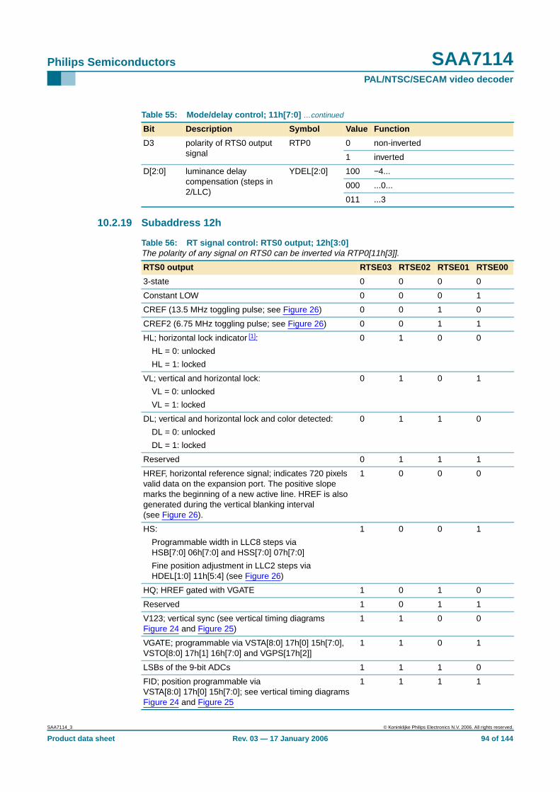
Philips Semiconductors SAA7114PAL/NTSC/SECAM video decoder
10.2.19 Subaddress 12h
D3 polarity of RTS0 outputsignal
RTP0 0 non-inverted
1 inverted
D[2:0] luminance delaycompensation (steps in2/LLC)
YDEL[2:0] 100 −4...
000 ...0...
011 ...3
Table 55: Mode/delay control; 11h[7:0] …continued
Bit Description Symbol Value Function
Table 56: RT signal control: RTS0 output; 12h[3:0]The polarity of any signal on RTS0 can be inverted via RTP0[11h[3]].
RTS0 output RTSE03 RTSE02 RTSE01 RTSE00
3-state 0 0 0 0
Constant LOW 0 0 0 1
CREF (13.5 MHz toggling pulse; see Figure 26) 0 0 1 0
CREF2 (6.75 MHz toggling pulse; see Figure 26) 0 0 1 1
HL; horizontal lock indicator [1]:
HL = 0: unlocked
HL = 1: locked
0 1 0 0
VL; vertical and horizontal lock:
VL = 0: unlocked
VL = 1: locked
0 1 0 1
DL; vertical and horizontal lock and color detected:
DL = 0: unlocked
DL = 1: locked
0 1 1 0
Reserved 0 1 1 1
HREF, horizontal reference signal; indicates 720 pixelsvalid data on the expansion port. The positive slopemarks the beginning of a new active line. HREF is alsogenerated during the vertical blanking interval(see Figure 26).
1 0 0 0
HS:
Programmable width in LLC8 steps viaHSB[7:0] 06h[7:0] and HSS[7:0] 07h[7:0]
Fine position adjustment in LLC2 steps viaHDEL[1:0] 11h[5:4] (see Figure 26)
1 0 0 1
HQ; HREF gated with VGATE 1 0 1 0
Reserved 1 0 1 1
V123; vertical sync (see vertical timing diagramsFigure 24 and Figure 25)
1 1 0 0
VGATE; programmable via VSTA[8:0] 17h[0] 15h[7:0],VSTO[8:0] 17h[1] 16h[7:0] and VGPS[17h[2]]
1 1 0 1
LSBs of the 9-bit ADCs 1 1 1 0
FID; position programmable viaVSTA[8:0] 17h[0] 15h[7:0]; see vertical timing diagramsFigure 24 and Figure 25
1 1 1 1
SAA7114_3 © Koninklijke Philips Electronics N.V. 2006. All rights reserved.
Product data sheet Rev. 03 — 17 January 2006 94 of 144
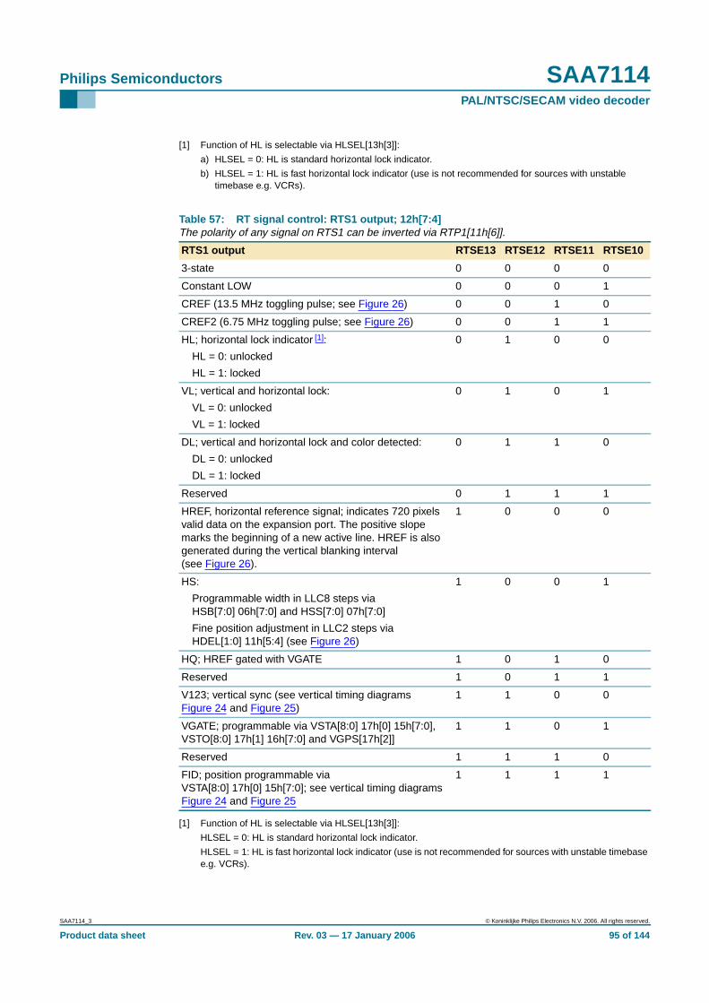
Philips Semiconductors SAA7114PAL/NTSC/SECAM video decoder
[1] Function of HL is selectable via HLSEL[13h[3]]:
a) HLSEL = 0: HL is standard horizontal lock indicator.
b) HLSEL = 1: HL is fast horizontal lock indicator (use is not recommended for sources with unstabletimebase e.g. VCRs).
[1] Function of HL is selectable via HLSEL[13h[3]]:
HLSEL = 0: HL is standard horizontal lock indicator.
HLSEL = 1: HL is fast horizontal lock indicator (use is not recommended for sources with unstable timebasee.g. VCRs).
Table 57: RT signal control: RTS1 output; 12h[7:4]The polarity of any signal on RTS1 can be inverted via RTP1[11h[6]].
RTS1 output RTSE13 RTSE12 RTSE11 RTSE10
3-state 0 0 0 0
Constant LOW 0 0 0 1
CREF (13.5 MHz toggling pulse; see Figure 26) 0 0 1 0
CREF2 (6.75 MHz toggling pulse; see Figure 26) 0 0 1 1
HL; horizontal lock indicator [1]:
HL = 0: unlocked
HL = 1: locked
0 1 0 0
VL; vertical and horizontal lock:
VL = 0: unlocked
VL = 1: locked
0 1 0 1
DL; vertical and horizontal lock and color detected:
DL = 0: unlocked
DL = 1: locked
0 1 1 0
Reserved 0 1 1 1
HREF, horizontal reference signal; indicates 720 pixelsvalid data on the expansion port. The positive slopemarks the beginning of a new active line. HREF is alsogenerated during the vertical blanking interval(see Figure 26).
1 0 0 0
HS:
Programmable width in LLC8 steps viaHSB[7:0] 06h[7:0] and HSS[7:0] 07h[7:0]
Fine position adjustment in LLC2 steps viaHDEL[1:0] 11h[5:4] (see Figure 26)
1 0 0 1
HQ; HREF gated with VGATE 1 0 1 0
Reserved 1 0 1 1
V123; vertical sync (see vertical timing diagramsFigure 24 and Figure 25)
1 1 0 0
VGATE; programmable via VSTA[8:0] 17h[0] 15h[7:0],VSTO[8:0] 17h[1] 16h[7:0] and VGPS[17h[2]]
1 1 0 1
Reserved 1 1 1 0
FID; position programmable viaVSTA[8:0] 17h[0] 15h[7:0]; see vertical timing diagramsFigure 24 and Figure 25
1 1 1 1
SAA7114_3 © Koninklijke Philips Electronics N.V. 2006. All rights reserved.
Product data sheet Rev. 03 — 17 January 2006 95 of 144
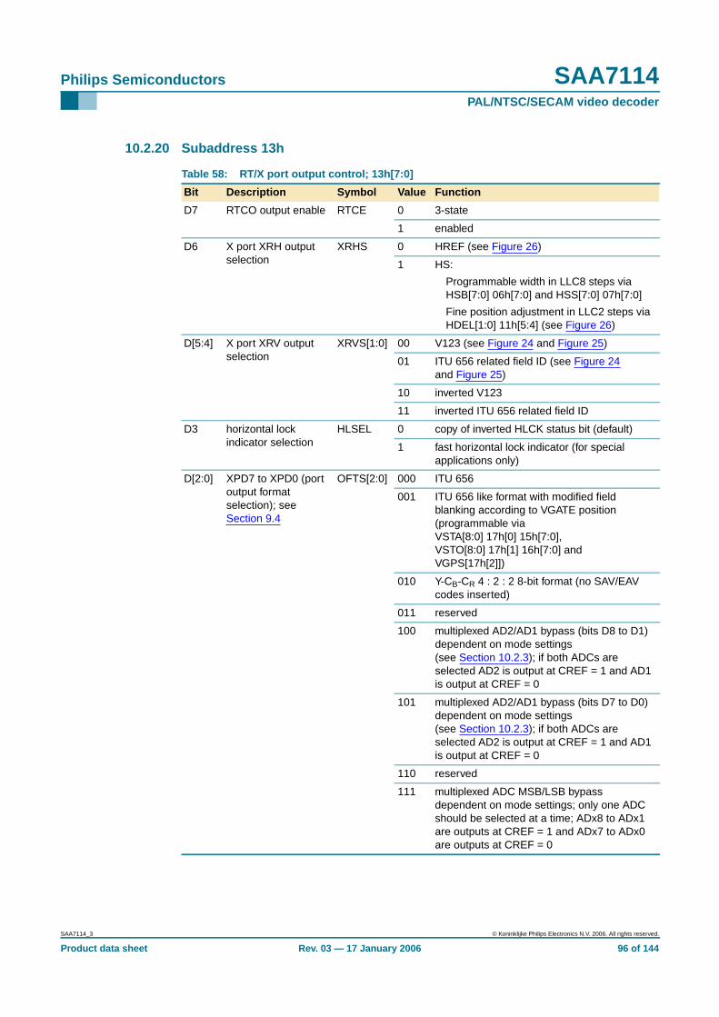
Philips Semiconductors SAA7114PAL/NTSC/SECAM video decoder
10.2.20 Subaddress 13h
Table 58: RT/X port output control; 13h[7:0]
Bit Description Symbol Value Function
D7 RTCO output enable RTCE 0 3-state
1 enabled
D6 X port XRH outputselection
XRHS 0 HREF (see Figure 26)
1 HS:
Programmable width in LLC8 steps viaHSB[7:0] 06h[7:0] and HSS[7:0] 07h[7:0]
Fine position adjustment in LLC2 steps viaHDEL[1:0] 11h[5:4] (see Figure 26)
D[5:4] X port XRV outputselection
XRVS[1:0] 00 V123 (see Figure 24 and Figure 25)
01 ITU 656 related field ID (see Figure 24and Figure 25)
10 inverted V123
11 inverted ITU 656 related field ID
D3 horizontal lockindicator selection
HLSEL 0 copy of inverted HLCK status bit (default)
1 fast horizontal lock indicator (for specialapplications only)
D[2:0] XPD7 to XPD0 (portoutput formatselection); seeSection 9.4
OFTS[2:0] 000 ITU 656
001 ITU 656 like format with modified fieldblanking according to VGATE position(programmable viaVSTA[8:0] 17h[0] 15h[7:0],VSTO[8:0] 17h[1] 16h[7:0] andVGPS[17h[2]])
010 Y-CB-CR 4 : 2 : 2 8-bit format (no SAV/EAVcodes inserted)
011 reserved
100 multiplexed AD2/AD1 bypass (bits D8 to D1)dependent on mode settings(see Section 10.2.3); if both ADCs areselected AD2 is output at CREF = 1 and AD1is output at CREF = 0
101 multiplexed AD2/AD1 bypass (bits D7 to D0)dependent on mode settings(see Section 10.2.3); if both ADCs areselected AD2 is output at CREF = 1 and AD1is output at CREF = 0
110 reserved
111 multiplexed ADC MSB/LSB bypassdependent on mode settings; only one ADCshould be selected at a time; ADx8 to ADx1are outputs at CREF = 1 and ADx7 to ADx0are outputs at CREF = 0
SAA7114_3 © Koninklijke Philips Electronics N.V. 2006. All rights reserved.
Product data sheet Rev. 03 — 17 January 2006 96 of 144
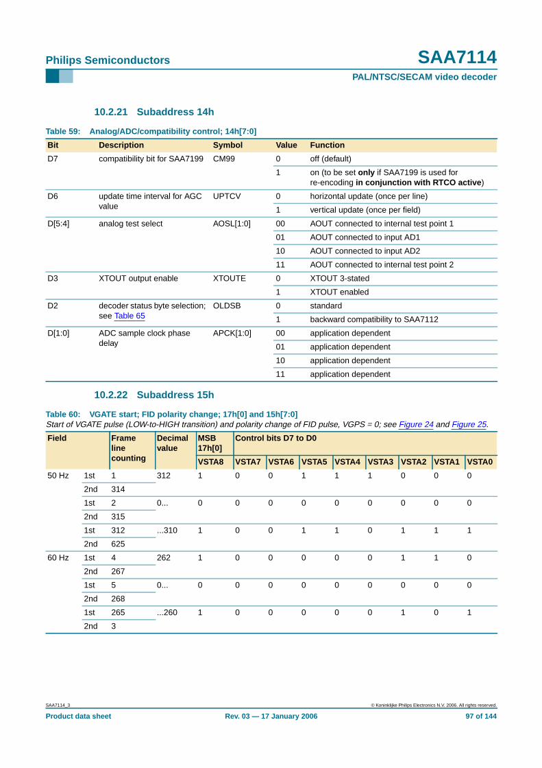
Philips Semiconductors SAA7114PAL/NTSC/SECAM video decoder
10.2.21 Subaddress 14h
10.2.22 Subaddress 15h
Table 59: Analog/ADC/compatibility control; 14h[7:0]
Bit Description Symbol Value Function
D7 compatibility bit for SAA7199 CM99 0 off (default)
1 on (to be set only if SAA7199 is used forre-encoding in conjunction with RTCO active )
D6 update time interval for AGCvalue
UPTCV 0 horizontal update (once per line)
1 vertical update (once per field)
D[5:4] analog test select AOSL[1:0] 00 AOUT connected to internal test point 1
01 AOUT connected to input AD1
10 AOUT connected to input AD2
11 AOUT connected to internal test point 2
D3 XTOUT output enable XTOUTE 0 XTOUT 3-stated
1 XTOUT enabled
D2 decoder status byte selection;see Table 65
OLDSB 0 standard
1 backward compatibility to SAA7112
D[1:0] ADC sample clock phasedelay
APCK[1:0] 00 application dependent
01 application dependent
10 application dependent
11 application dependent
Table 60: VGATE start; FID polarity change; 17h[0] and 15h[7:0]Start of VGATE pulse (LOW-to-HIGH transition) and polarity change of FID pulse, VGPS = 0; see Figure 24 and Figure 25.
Field Framelinecounting
Decimalvalue
MSB17h[0]
Control bits D7 to D0
VSTA8 VSTA7 VSTA6 VSTA5 VSTA4 VSTA3 VSTA2 VSTA1 VSTA0
50 Hz 1st 1 312 1 0 0 1 1 1 0 0 0
2nd 314
1st 2 0... 0 0 0 0 0 0 0 0 0
2nd 315
1st 312 ...310 1 0 0 1 1 0 1 1 1
2nd 625
60 Hz 1st 4 262 1 0 0 0 0 0 1 1 0
2nd 267
1st 5 0... 0 0 0 0 0 0 0 0 0
2nd 268
1st 265 ...260 1 0 0 0 0 0 1 0 1
2nd 3
SAA7114_3 © Koninklijke Philips Electronics N.V. 2006. All rights reserved.
Product data sheet Rev. 03 — 17 January 2006 97 of 144
Philips Semiconductors SAA7114PAL/NTSC/SECAM video decoder
10.2.23 Subaddress 16h
10.2.24 Subaddress 17h
10.2.25 Subaddress 18h
Table 61: VGATE stop; 17h[1] and 16h[7:0]Stop of VGATE pulse (HIGH-to-LOW transition), VGPS = 0; see Figure 24 and Figure 25.
Field Framelinecounting
Decimalvalue
MSB17h[1]
Control bits D7 to D0
VSTO8 VSTO7 VSTO6 VSTO5 VSTO4 VSTO3 VSTO2 VSTO1 VSTO0
50 Hz 1st 1 312 1 0 0 1 1 1 0 0 0
2nd 314
1st 2 0... 0 0 0 0 0 0 0 0 0
2nd 315
1st 312 ...310 1 0 0 1 1 0 1 1 1
2nd 625
60 Hz 1st 4 262 1 0 0 0 0 0 1 1 0
2nd 267
1st 5 0... 0 0 0 0 0 0 0 0 0
2nd 268
1st 265 ...260 1 0 0 0 0 0 1 0 1
2nd 3
Table 62: Miscellaneous/VGATE MSBs; 17h[7:6] and 17h[2:0]
Bit Description Symbol Value Function
D7 LLC output enable LLCE 0 enable
1 3-state
D6 LLC2 output enable LLC2E 0 enable
1 3-state
D2 alternative VGATE position VGPS 0 VGATE position according to Table 60 andTable 61
1 VGATE occurs one line earlier during field 2
D1 MSB VGATE stop VSTO8 see Table 61
D0 MSB VGATE start VSTA8 see Table 60
Table 63: Raw data gain control; RAWG[7:0]18h[7:0]; see Figure 19
Gain Control bits D7 to D0
RAWG7 RAWG6 RAWG5 RAWG4 RAWG3 RAWG2 RAWG1 RAWG0
255 (double amplitude) 0 1 1 1 1 1 1 1
128 (nominal level) 0 1 0 0 0 0 0 0
0 (off) 0 0 0 0 0 0 0 0
SAA7114_3 © Koninklijke Philips Electronics N.V. 2006. All rights reserved.
Product data sheet Rev. 03 — 17 January 2006 98 of 144
Philips Semiconductors SAA7114PAL/NTSC/SECAM video decoder
10.2.26 Subaddress 19h
10.2.27 Subaddress 1Fh
Table 64: Raw data offset control; RAWO[7:0] 19h[7:0]; see Figure 19
Offset Control bits D7 to D0
RAWO7 RAWO6 RAWO5 RAWO4 RAWO3 RAWO2 RAWO1 RAWO0
−128 LSB 0 0 0 0 0 0 0 0
0 LSB 1 0 0 0 0 0 0 0
+128 LSB 1 1 1 1 1 1 1 1
Table 65: Status byte video decoder; 1Fh[7:0]; read only register
Bit Description I2C-buscontrol bit
OLDSB14h[2]
Value Function
D7 status bit for interlace detection INTL - 0 non-interlaced
1 interlaced
D6 status bit for horizontal and vertical loop HLVLN 0 0 both loopslocked
1 unlocked
status bit for locked horizontal frequency HLCK 1 0 locked
1 unlocked
D5 identification bit for detected fieldfrequency
FIDT - 0 50 Hz
1 60 Hz
D4 gain value for active luminance channelis limited; maximum (top)
GLIMT - 0 not active
1 active
D3 gain value for active luminance channelis limited; minimum (bottom)
GLIMB - 0 not active
1 active
D2 white peak loop is activated WIPA - 0 not active
1 active
D1 copy protected source detectedaccording to Macrovision version up to7.01
COPRO 0 0 not active
1 active
slow time constant active in WIPA mode SLTCA 1 0 not active
1 active
D0 ready for capture (all internal loopslocked)
RDCAP 0 0 not active
1 active
color signal in accordance with selectedstandard has been detected
CODE 1 0 not active
1 active
SAA7114_3 © Koninklijke Philips Electronics N.V. 2006. All rights reserved.
Product data sheet Rev. 03 — 17 January 2006 99 of 144
Philips Semiconductors SAA7114PAL/NTSC/SECAM video decoder
10.3 Programming register audio clock generationSee equations in Section 8.6 and examples in Table 22 and Table 23.
10.3.1 Subaddresses 30h to 32h
10.3.2 Subaddresses 34h to 36h
10.3.3 Subaddress 38h
10.3.4 Subaddress 39h
10.3.5 Subaddress 3Ah
Table 66: Audio master clock (AMCLK) cycles per field
Subaddress Control bits D7 to D0
30h ACPF7 ACPF6 ACPF5 ACPF4 ACPF3 ACPF2 ACPF1 ACPF0
31h ACPF15 ACPF14 ACPF13 ACPF12 ACPF11 ACPF10 ACPF9 ACPF8
32h - - - - - - ACPF17 ACPF16
Table 67: Audio master clock (AMCLK) nominal increment
Subaddress Control bits D7 to D0
34h ACNI7 ACNI6 ACNI5 ACNI4 ACNI3 ACNI2 ACNI1 ACNI0
35h ACNI15 ACNI14 ACNI13 ACNI12 ACNI11 ACNI10 ACNI9 ACNI8
36h - - ACNI21 ACNI20 ACNI19 ACNI18 ACNI17 ACNI16
Table 68: Clock ratio audio master clock (AMXCLK) to serial bit clock (ASCLK)
Subaddress Control bits D7 to D0
38h - - SDIV5 SDIV4 SDIV3 SDIV2 SDIV1 SDIV0
Table 69: Clock ratio serial bit clock (ASCLK) to channel select clock (ALRCLK)
Subaddress Control bits D7 to D0
39h - - LRDIV5 LRDIV4 LRDIV3 LRDIV2 LRDIV1 LRDIV0
Table 70: Audio clock control; 3Ah[3:0]
Bit Description Symbol Value Function
D3 audio PLL modes APLL 0 PLL active, AMCLK is field-locked
1 PLL open, AMCLK is free-running
D2 audio master clockvertical reference
AMVR 0 vertical reference pulse is taken from internaldecoder
1 vertical reference is taken from XRV input(expansion port)
D1 ALRCLK phase LRPH 0 ALRCLK edges triggered by falling edges ofASCLK
1 ALRCLK edges triggered by rising edges ofASCLK
D0 ASCLK phase SCPH 0 ASCLK edges triggered by falling edges ofAMCLK
1 ASCLK edges triggered by rising edges of AMCLK
SAA7114_3 © Koninklijke Philips Electronics N.V. 2006. All rights reserved.
Product data sheet Rev. 03 — 17 January 2006 100 of 144
Philips Semiconductors SAA7114PAL/NTSC/SECAM video decoder
10.4 Programming register VBI data slicer
10.4.1 Subaddress 40h
10.4.2 Subaddresses 41h to 57h
Table 71: Slicer control 1; 40h[6:4]
Bit Description Symbol Value Function
D6 Hamming check HAM_N 0 Hamming check for 2 bytes after framingcode, dependent on data type (default)
1 no Hamming check
D5 framing code error FCE 0 one framing code error allowed
1 no framing code errors allowed
D4 amplitude searching HUNT_N 0 amplitude searching active (default)
1 amplitude searching stopped
Table 72: Line control register; LCR2 to LCR24 (41h to 57h)See Section 8.2 and Section 8.4.
Name Description Framing code D[7:4](41h to 57h)
D[3:0](41h to 57h)
DT[3:0] 62h[3:0](field 1)
DT[3:0] 62h[3:0](field 2)
WST625 teletext EuroWST, CCST 27h 0000 0000
CC625 European closed caption 001 0001 0001
VPS video programming service 9951h 0010 0010
WSS wide screen signalling bits 1E 3C1Fh 0011 0011
WST525 US teletext (WST) 27h 0100 0100
CC525 US closed caption (line 21) 001 0101 0101
Test line video component signal, VBIregion
- 0110 0110
Intercast raw data - 0111 0111
General text teletext programmable 1000 1000
VITC625 VITC/EBU time codes(Europe)
programmable 1001 1001
VITC525 VITC/SMPTE time codes(USA)
programmable 1010 1010
Reserved reserved - 1011 1011
NABTS US NABTS - 1100 1100
Japtext MOJI (Japanese) programmable(A7h)
1101 1101
JFS Japanese format switch(L20/22)
programmable 1110 1110
Active video video component signal,active video region (default)
- 1111 1111
SAA7114_3 © Koninklijke Philips Electronics N.V. 2006. All rights reserved.
Product data sheet Rev. 03 — 17 January 2006 101 of 144
Philips Semiconductors SAA7114PAL/NTSC/SECAM video decoder
10.4.3 Subaddress 58h
10.4.4 Subaddress 59h
10.4.5 Subaddress 5Ah
10.4.6 Subaddress 5Bh
10.4.7 Subaddress 5Dh
Table 73: Programmable framing code; slicer set 58h[7:0]According to Table 15 and Table 72.
Framing code for programmable data types Control bits D7 to D0
Default value FC[7:0] = 40h
Table 74: Horizontal offset for slicer; slicer set 59h and 5Bh
Horizontal offset Control bits 5Bh[2:0] Control bits 59h[7:0]
Recommended value HOFF[10:8] = 3h HOFF[7:0] = 47h
Table 75: Vertical offset for slicer; slicer set 5Ah and 5Bh
Vertical offset Control bit 5Bh[4] Control bits 5Ah[7:0]
VOFF8 VOFF[7:0]
Minimum value 0 0 00h
Maximum value 312 1 38h
Value for 50 Hz 625 lines input 0 03h
Value for 60 Hz 525 lines input 0 06h
Table 76: Field offset, and MSBs for horizontal and vertical offsets; slicer set 5Bh[7:6]See Section 10.4.4 and Section 10.4.5 for HOFF[10:8] 5Bh[2:0] and VOFF8[5Bh[4]].
Bit Description Symbol Value Function
D7 field offset FOFF 0 no modification of internal field indicator (default for50 Hz 625 lines input sources)
1 invert field indicator (default for 60 Hz 525 lines inputsources)
D6 recode RECODE 0 leave data unchanged (default)
1 convert 00h and FFh data bytes into 03h and FCh
Table 77: Header and data identification (DID; ITU 656) code control; slicer set 5Dh[7:0]
Bit Description Symbol Value Function
D7 field ID and V-blankselection for text output(F and V referenceselection)
FVREF 0 F and V output of slicer is LCR tabledependent
1 F and V output is taken from decoderreal-time signals EVEN_ITU andVBLNK_ITU
D[5:0] default; DID[5:0] = 00h DID[5:0] 00 0000 ANC header framing ; see Figure 33and Table 21
special cases of DIDprogramming
11 1110 DID[5:0] = 3Eh SAV/EAV framing, withFVREF = 1
11 1111 DID[5:0] = 3Fh SAV/EAV framing, withFVREF = 0
SAA7114_3 © Koninklijke Philips Electronics N.V. 2006. All rights reserved.
Product data sheet Rev. 03 — 17 January 2006 102 of 144
Philips Semiconductors SAA7114PAL/NTSC/SECAM video decoder
10.4.8 Subaddress 5Eh
10.4.9 Subaddress 60h
10.4.10 Subaddresses 61h and 62h
10.5 Programming register interfaces and scaler part
10.5.1 Subaddress 80h
Table 78: Sliced data identification (SDID) code; slicer set 5Eh[5:0]
Bit Description Symbol Value Function
D[5:0] SDID codes SDID[5:0] 00h default
Table 79: Slicer status byte 0; 60h[6:2]; read only register
Bit Description Symbol Value Function
D6 framing code valid FC8V 0 no framing code (0 error) in the last framedetected
1 framing code with 0 error detected
D5 framing code valid FC7V 0 no framing code (1 error) in the last framedetected
1 framing code with 1 error detected
D4 VPS valid VPSV 0 no VPS in the last frame
1 VPS detected
D3 PALplus valid PPV 0 no PALplus in the last frame
1 PALplus detected
D2 closed caption valid CCV 0 no closed caption in the last frame
1 closed caption detected
Table 80: Slicer status byte 1; 61h[5:0] and slicer status byte 2; 62h[7:0]; read onlyregisters
Subaddress Bit Symbol Description
61h D5 F21_N field ID as seen by the VBI slicer; for field 1:D5 = 0
D[4:0] LN[8:4] line number
62h D[7:4] LN[3:0] line number
D[3:0] DT[3:0] data type; according to Table 15
Table 81: Global control 1; global set 80h[6:4] [1]
SWRST moved to subaddress 88h[5].
Task enable control Control bits D6 to D4
SMOD TEB TEA
Task of register set A is disabled X X 0
Task of register set A is enabled X X 1
Task of register set B is disabled X 0 X
Task of register set B is enabled X 1 X
The scaler window defines the F and V timing of the scaler output 0 X X
VBI data slicer defines the F and V timing of the scaler output 1 X X
SAA7114_3 © Koninklijke Philips Electronics N.V. 2006. All rights reserved.
Product data sheet Rev. 03 — 17 January 2006 103 of 144
Philips Semiconductors SAA7114PAL/NTSC/SECAM video decoder
[1] X = don’t care.
[1] X = don’t care.
[2] Although the ICLKO I/O is independent of ICKS2 and ICKS3, this selection can only be used if ICKS2 = 1.
10.5.2 Subaddresses 83h to 87h
[1] X = don’t care.
Table 82: Global control 1; global set 80h[3:0] [1]
I port and scaler back-end clock selection Control bits D3 to D0
ICKS3 ICKS2 ICKS1 ICKS0
ICLK output and back-end clock is line-locked clock LLC fromdecoder
X X 0 0
ICLK output and back-end clock is XCLK from X port X X 0 1
ICLK output is LLC and back-end clock is LLC2 clock X X [2] 1 0
Back-end clock is the ICLK input X X 1 1
IDQ pin carries the data qualifier X 0 X X
IDQ pin carries a gated back-end clock (DQ AND CLK) X 1 X X
IDQ generation only for valid data 0 X X X
IDQ qualifies valid data inside the scaling region and all dataoutside the scaling region
1 X X X
Table 83: X port I/O enable and output clock phase control; global set 83h[5:4]
Output clock phase control Control bits D5 and D4
XPCK1 XPCK0
XCLK default output phase, recommended value 0 0
XCLK output inverted 0 1
XCLK phase shifted by approximately 3 ns 1 0
XCLK output inverted and shifted by approximately 3 ns 1 1
Table 84: X port I/O enable and output clock phase control; global set 83h[2:0] [1]
X port I/O enable Control bits D2 to D0
XRQT XPE1 XPE0
X port output is disabled by software X 0 0
X port output is enabled by software X 0 1
X port output is enabled by pin XTRI at logic 0 X 1 0
X port output is enabled by pin XTRI at logic 1 X 1 1
XRDY output signal is A/B task flag from event handler (A = 1) 0 X X
XRDY output signal is ready signal from scaler path (XRDY = 1means the SAA7114 is ready to receive data)
1 X X
SAA7114_3 © Koninklijke Philips Electronics N.V. 2006. All rights reserved.
Product data sheet Rev. 03 — 17 January 2006 104 of 144
Philips Semiconductors SAA7114PAL/NTSC/SECAM video decoder
[1] X = don’t care.
Table 85: I port signal definitions; global set 84h[7:6] and 86h[5]
I port signal definitions Control bits
86h[5] 84h[7:6]
IDG02 IDG01 IDG00
IGP0 is output field ID, as defined by OFIDC[90h[6]] 0 0 0
IGP0 is A/B task flag, as defined by CONLH[90h[7]] 0 0 1
IGP0 is sliced data flag, framing the sliced VBI data at the I port 0 1 0
IGP0 is set to logic 0 (default polarity) 0 1 1
IGP0 is the output FIFO almost filled flag 1 0 0
IGP0 is the output FIFO overflow flag 1 0 1
IGP0 is the output FIFO almost full flag, level to be programmed insubaddress 86h
1 1 0
IGP0 is the output FIFO almost empty flag, level to be programmed insubaddress 86h
1 1 1
Table 86: I port signal definitions; global set 84h[5:4] and 86h[4]
I port signal definitions Control bits
86h[4] 84h[5:4]
IDG12 IDG11 IDG10
IGP1 is output field ID, as defined by OFIDC[90h[6]] 0 0 0
IGP1 is A/B task flag, as defined by CONLH[90h[7]] 0 0 1
IGP1 is sliced data flag, framing the sliced VBI data at the I port 0 1 0
IGP1 is set to logic 0 (default polarity) 0 1 1
IGP1 is the output FIFO almost filled flag 1 0 0
IGP1 is the output FIFO overflow flag 1 0 1
IGP1 is the output FIFO almost full flag, level to be programmed insubaddress 86h
1 1 0
IGP1 is the output FIFO almost empty flag, level to be programmed insubaddress 86h
1 1 1
Table 87: I port output signal definitions; global set 84h[3:0] [1]
I port output signal definitions Control bits D3 to D0
IDV1 IDV0 IDH1 IDH0
IGPH is a H gate signal, framing the scaler output X X 0 0
IGPH is an extended H gate (framing H gate during scaler output andscaler input H reference outside the scaler window)
X X 0 1
IGPH is a horizontal trigger pulse, on active going edge of H gate X X 1 0
IGPH is a horizontal trigger pulse, on active going edge of extendedH gate
X X 1 1
IGPV is a V gate signal, framing scaled output lines 0 0 X X
IGPV is the V reference signal from scaler input 0 1 X X
IGPV is a vertical trigger pulse, derived from V gate 1 0 X X
IGPV is a vertical trigger pulse derived from input V reference 1 1 X X
SAA7114_3 © Koninklijke Philips Electronics N.V. 2006. All rights reserved.
Product data sheet Rev. 03 — 17 January 2006 105 of 144
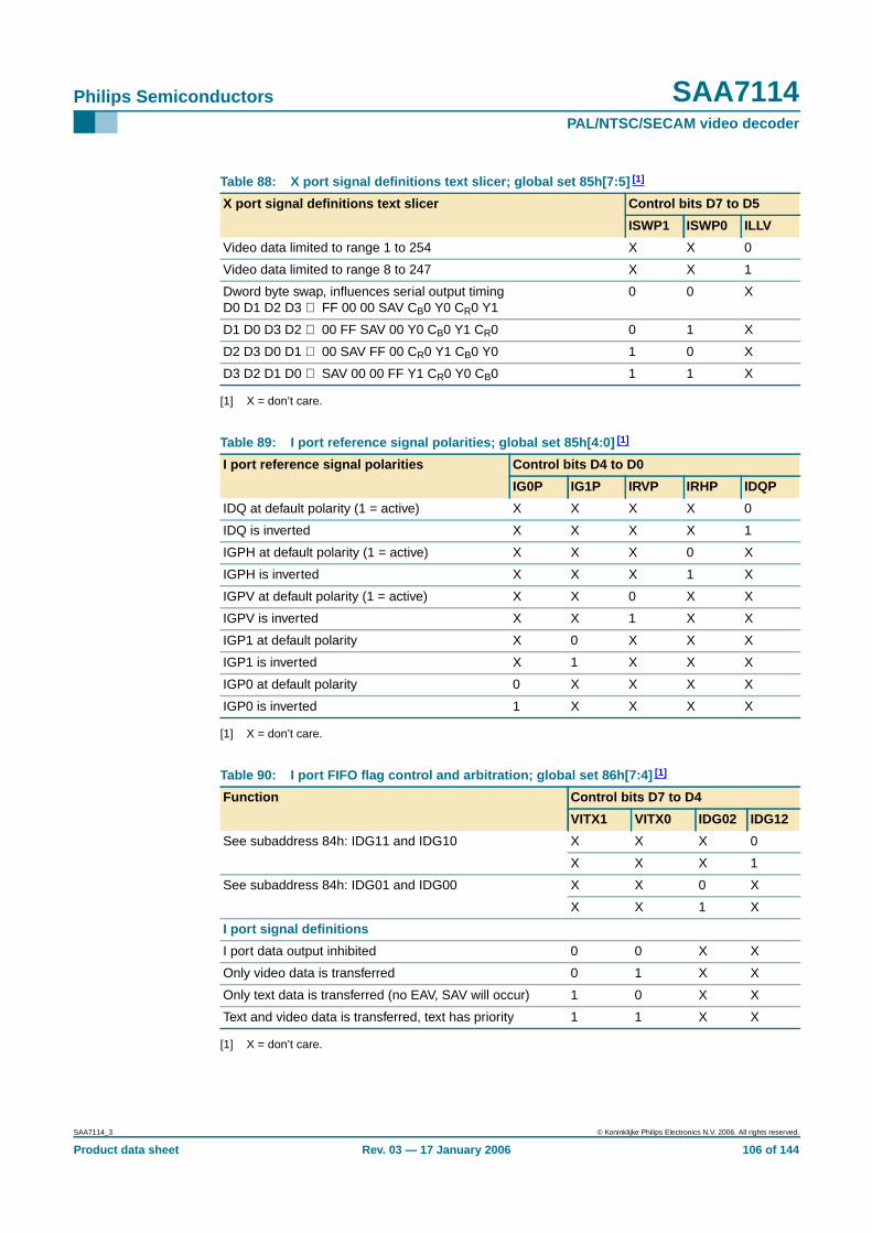
Philips Semiconductors SAA7114PAL/NTSC/SECAM video decoder
[1] X = don’t care.
[1] X = don’t care.
[1] X = don’t care.
Table 88: X port signal definitions text slicer; global set 85h[7:5] [1]
X port signal definitions text slicer Control bits D7 to D5
ISWP1 ISWP0 ILLV
Video data limited to range 1 to 254 X X 0
Video data limited to range 8 to 247 X X 1
Dword byte swap, influences serial output timingD0 D1 D2 D3 ⇒ FF 00 00 SAV CB0 Y0 CR0 Y1
0 0 X
D1 D0 D3 D2 ⇒ 00 FF SAV 00 Y0 CB0 Y1 CR0 0 1 X
D2 D3 D0 D1 ⇒ 00 SAV FF 00 CR0 Y1 CB0 Y0 1 0 X
D3 D2 D1 D0 ⇒ SAV 00 00 FF Y1 CR0 Y0 CB0 1 1 X
Table 89: I port reference signal polarities; global set 85h[4:0] [1]
I port reference signal polarities Control bits D4 to D0
IG0P IG1P IRVP IRHP IDQP
IDQ at default polarity (1 = active) X X X X 0
IDQ is inverted X X X X 1
IGPH at default polarity (1 = active) X X X 0 X
IGPH is inverted X X X 1 X
IGPV at default polarity (1 = active) X X 0 X X
IGPV is inverted X X 1 X X
IGP1 at default polarity X 0 X X X
IGP1 is inverted X 1 X X X
IGP0 at default polarity 0 X X X X
IGP0 is inverted 1 X X X X
Table 90: I port FIFO flag control and arbitration; global set 86h[7:4] [1]
Function Control bits D7 to D4
VITX1 VITX0 IDG02 IDG12
See subaddress 84h: IDG11 and IDG10 X X X 0
X X X 1
See subaddress 84h: IDG01 and IDG00 X X 0 X
X X 1 X
I port signal definitions
I port data output inhibited 0 0 X X
Only video data is transferred 0 1 X X
Only text data is transferred (no EAV, SAV will occur) 1 0 X X
Text and video data is transferred, text has priority 1 1 X X
SAA7114_3 © Koninklijke Philips Electronics N.V. 2006. All rights reserved.
Product data sheet Rev. 03 — 17 January 2006 106 of 144
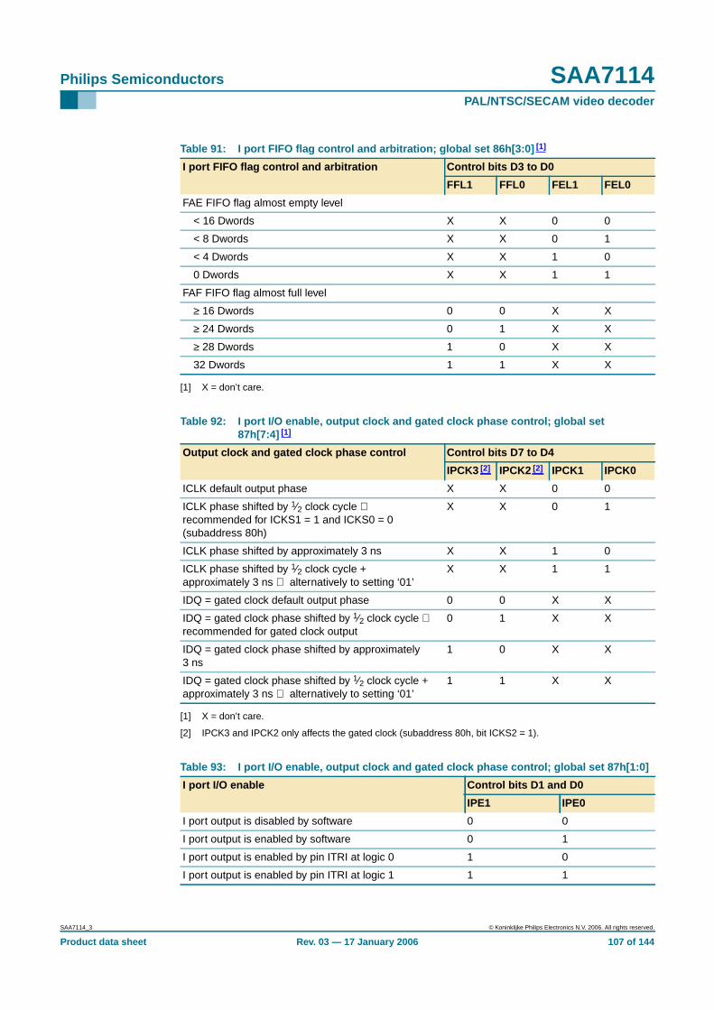
Philips Semiconductors SAA7114PAL/NTSC/SECAM video decoder
[1] X = don’t care.
[1] X = don’t care.
[2] IPCK3 and IPCK2 only affects the gated clock (subaddress 80h, bit ICKS2 = 1).
Table 91: I port FIFO flag control and arbitration; global set 86h[3:0] [1]
I port FIFO flag control and arbitration Control bits D3 to D0
FFL1 FFL0 FEL1 FEL0
FAE FIFO flag almost empty level
< 16 Dwords X X 0 0
< 8 Dwords X X 0 1
< 4 Dwords X X 1 0
0 Dwords X X 1 1
FAF FIFO flag almost full level
≥ 16 Dwords 0 0 X X
≥ 24 Dwords 0 1 X X
≥ 28 Dwords 1 0 X X
32 Dwords 1 1 X X
Table 92: I port I/O enable, output clock and gated clock phase control; global set87h[7:4] [1]
Output clock and gated clock phase control Control bits D7 to D4
IPCK3 [2] IPCK2 [2] IPCK1 IPCK0
ICLK default output phase X X 0 0
ICLK phase shifted by 1⁄2 clock cycle ⇒recommended for ICKS1 = 1 and ICKS0 = 0(subaddress 80h)
X X 0 1
ICLK phase shifted by approximately 3 ns X X 1 0
ICLK phase shifted by 1⁄2 clock cycle +approximately 3 ns ⇒ alternatively to setting ‘01’
X X 1 1
IDQ = gated clock default output phase 0 0 X X
IDQ = gated clock phase shifted by 1⁄2 clock cycle ⇒recommended for gated clock output
0 1 X X
IDQ = gated clock phase shifted by approximately3 ns
1 0 X X
IDQ = gated clock phase shifted by 1⁄2 clock cycle +approximately 3 ns ⇒ alternatively to setting ‘01’
1 1 X X
Table 93: I port I/O enable, output clock and gated clock phase control; global set 87h[1:0]
I port I/O enable Control bits D1 and D0
IPE1 IPE0
I port output is disabled by software 0 0
I port output is enabled by software 0 1
I port output is enabled by pin ITRI at logic 0 1 0
I port output is enabled by pin ITRI at logic 1 1 1
SAA7114_3 © Koninklijke Philips Electronics N.V. 2006. All rights reserved.
Product data sheet Rev. 03 — 17 January 2006 107 of 144
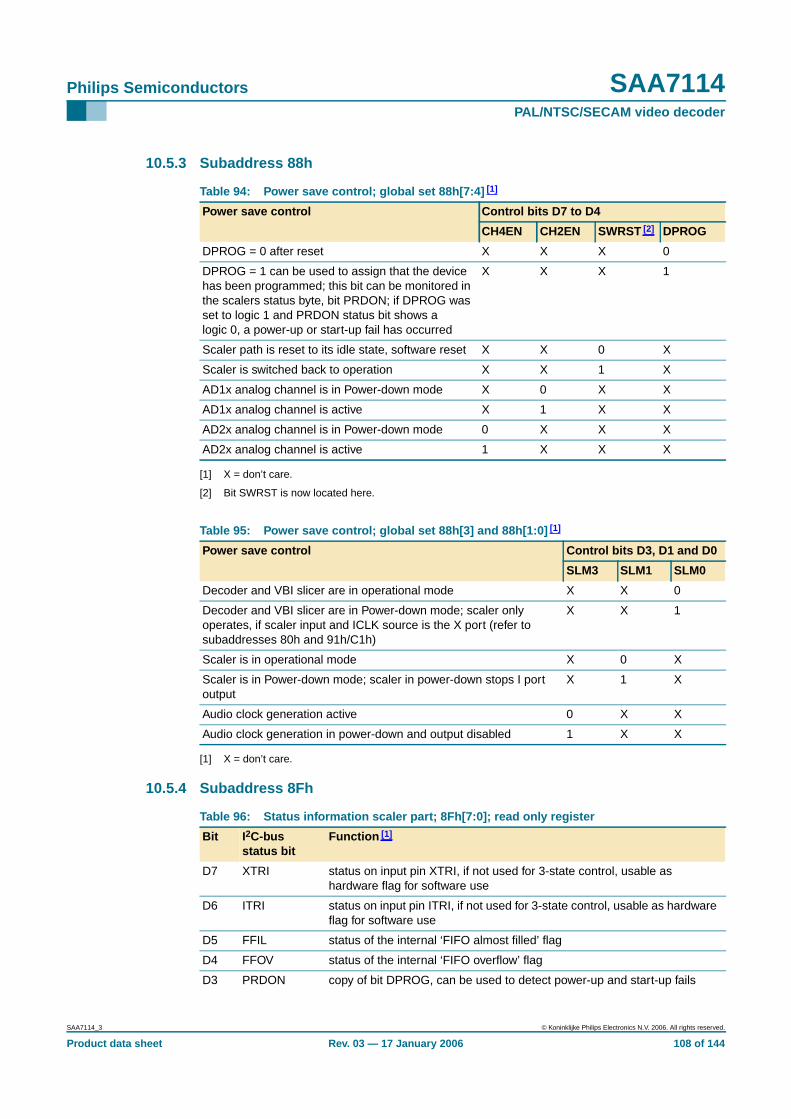
Philips Semiconductors SAA7114PAL/NTSC/SECAM video decoder
10.5.3 Subaddress 88h
[1] X = don’t care.
[2] Bit SWRST is now located here.
[1] X = don’t care.
10.5.4 Subaddress 8Fh
Table 94: Power save control; global set 88h[7:4] [1]
Power save control Control bits D7 to D4
CH4EN CH2EN SWRST [2] DPROG
DPROG = 0 after reset X X X 0
DPROG = 1 can be used to assign that the devicehas been programmed; this bit can be monitored inthe scalers status byte, bit PRDON; if DPROG wasset to logic 1 and PRDON status bit shows alogic 0, a power-up or start-up fail has occurred
X X X 1
Scaler path is reset to its idle state, software reset X X 0 X
Scaler is switched back to operation X X 1 X
AD1x analog channel is in Power-down mode X 0 X X
AD1x analog channel is active X 1 X X
AD2x analog channel is in Power-down mode 0 X X X
AD2x analog channel is active 1 X X X
Table 95: Power save control; global set 88h[3] and 88h[1:0] [1]
Power save control Control bits D3, D1 and D0
SLM3 SLM1 SLM0
Decoder and VBI slicer are in operational mode X X 0
Decoder and VBI slicer are in Power-down mode; scaler onlyoperates, if scaler input and ICLK source is the X port (refer tosubaddresses 80h and 91h/C1h)
X X 1
Scaler is in operational mode X 0 X
Scaler is in Power-down mode; scaler in power-down stops I portoutput
X 1 X
Audio clock generation active 0 X X
Audio clock generation in power-down and output disabled 1 X X
Table 96: Status information scaler part; 8Fh[7:0]; read only register
Bit I2C-busstatus bit
Function [1]
D7 XTRI status on input pin XTRI, if not used for 3-state control, usable ashardware flag for software use
D6 ITRI status on input pin ITRI, if not used for 3-state control, usable as hardwareflag for software use
D5 FFIL status of the internal ‘FIFO almost filled’ flag
D4 FFOV status of the internal ‘FIFO overflow’ flag
D3 PRDON copy of bit DPROG, can be used to detect power-up and start-up fails
SAA7114_3 © Koninklijke Philips Electronics N.V. 2006. All rights reserved.
Product data sheet Rev. 03 — 17 January 2006 108 of 144
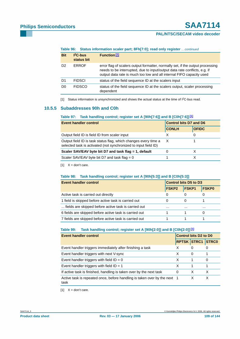
Philips Semiconductors SAA7114PAL/NTSC/SECAM video decoder
[1] Status information is unsynchronized and shows the actual status at the time of I2C-bus read.
10.5.5 Subaddresses 90h and C0h
[1] X = don’t care.
[1] X = don’t care.
D2 ERROF error flag of scalers output formatter, normally set, if the output processingneeds to be interrupted, due to input/output data rate conflicts, e.g. ifoutput data rate is much too low and all internal FIFO capacity used
D1 FIDSCI status of the field sequence ID at the scalers input
D0 FIDSCO status of the field sequence ID at the scalers output, scaler processingdependent
Table 96: Status information scaler part; 8Fh[7:0]; read only register …continued
Bit I2C-busstatus bit
Function [1]
Table 97: Task handling control; register set A [90h[7:6]] and B [C0h[7:6]] [1]
Event handler control Control bits D7 and D6
CONLH OFIDC
Output field ID is field ID from scaler input X 0
Output field ID is task status flag, which changes every time aselected task is activated (not synchronized to input field ID)
X 1
Scaler SAV/EAV byte bit D7 and task flag = 1, default 0 X
Scaler SAV/EAV byte bit D7 and task flag = 0 1 X
Table 98: Task handling control; register set A [90h[5:3]] and B [C0h[5:3]]
Event handler control Control bits D5 to D3
FSKP2 FSKP1 FSKP0
Active task is carried out directly 0 0 0
1 field is skipped before active task is carried out 0 0 1
... fields are skipped before active task is carried out ... ... ...
6 fields are skipped before active task is carried out 1 1 0
7 fields are skipped before active task is carried out 1 1 1
Table 99: Task handling control; register set A [90h[2:0]] and B [C0h[2:0]] [1]
Event handler control Control bits D2 to D0
RPTSK STRC1 STRC0
Event handler triggers immediately after finishing a task X 0 0
Event handler triggers with next V-sync X 0 1
Event handler triggers with field ID = 0 X 1 0
Event handler triggers with field ID = 1 X 1 1
If active task is finished, handling is taken over by the next task 0 X X
Active task is repeated once, before handling is taken over by the nexttask
1 X X
SAA7114_3 © Koninklijke Philips Electronics N.V. 2006. All rights reserved.
Product data sheet Rev. 03 — 17 January 2006 109 of 144
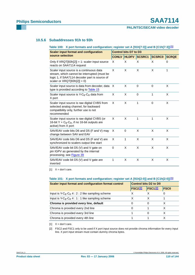
Philips Semiconductors SAA7114PAL/NTSC/SECAM video decoder
10.5.6 Subaddresses 91h to 93h
[1] X = don’t care.
[1] X = don’t care.
[2] FSC2 and FSC1 only to be used if X port input source does not provide chroma information for every inputline. X port input stream must contain dummy chroma bytes.
Table 100: X port formats and configuration; register set A [91h[7:3]] and B [C1h[7:3]] [1]
Scaler input format and configurationsource selection
Control bits D7 to D3
CONLV HLDFV SCSRC1 SCSRC0 SCRQE
Only if XRQT[83h[2]] = 1: scaler input sourcereacts on SAA7114 request
X X X X 0
Scaler input source is a continuous datastream, which cannot be interrupted (must belogic 1, if SAA7114 decoder part is source ofscaler or XRQT[83h[2]] = 0)
X X X X 1
Scaler input source is data from decoder, datatype is provided according to Table 15
X X 0 0 X
Scaler input source is Y-CB-CR data fromX port
X X 0 1 X
Scaler input source is raw digital CVBS fromselected analog channel, for backwardcompatibility only, further use is notrecommended
X X 1 0 X
Scaler input source is raw digital CVBS (or16-bit Y + CB-CR, if no 16-bit outputs areactive) from X port
X X 1 1 X
SAV/EAV code bits D6 and D5 (F and V) maychange between SAV and EAV
X 0 X X X
SAV/EAV code bits D6 and D5 (F and V) aresynchronized to scalers output line start
X 1 X X X
SAV/EAV code bit D5 (V) and V gate onpin IGPV as generated by the internalprocessing; see Figure 39
0 X X X X
SAV/EAV code bit D5 (V) and V gate areinverted
1 X X X X
Table 101: X port formats and configuration; register set A [91h[2:0]] and B [C1h[2:0]] [1]
Scaler input format and configuration format control Control bits D2 to D0
FSC2 [2] FSC1 [2] FSC0
Input is Y-CB-CR 4 : 2 : 2 like sampling scheme X X 0
Input is Y-CB-CR 4 : 1 : 1 like sampling scheme X X 1
Chroma is provided every line, default 0 0 X
Chroma is provided every 2nd line 0 1 X
Chroma is provided every 3rd line 1 0 X
Chroma is provided every 4th line 1 1 X
SAA7114_3 © Koninklijke Philips Electronics N.V. 2006. All rights reserved.
Product data sheet Rev. 03 — 17 January 2006 110 of 144
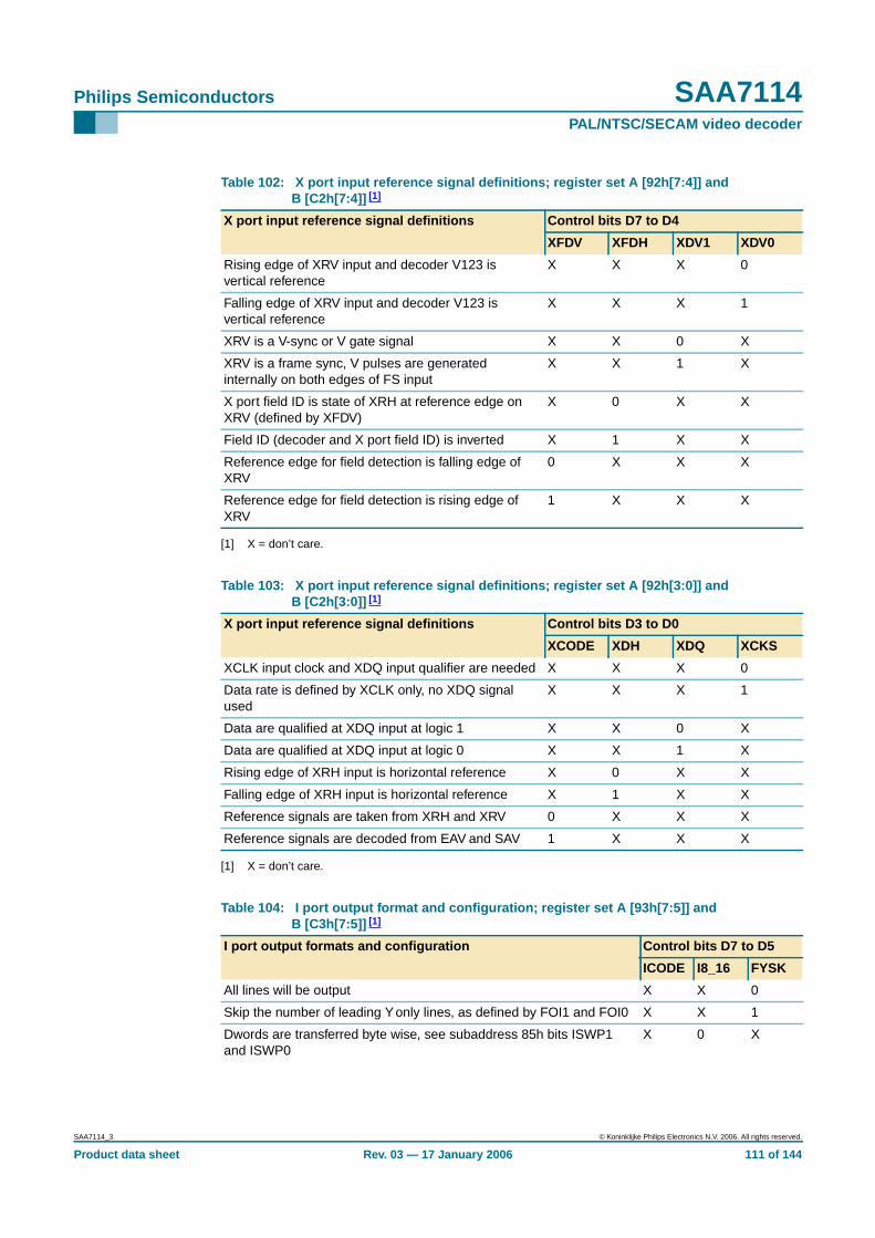
Philips Semiconductors SAA7114PAL/NTSC/SECAM video decoder
[1] X = don’t care.
[1] X = don’t care.
Table 102: X port input reference signal definitions; register set A [92h[7:4]] andB [C2h[7:4]] [1]
X port input reference signal definitions Control bits D7 to D4
XFDV XFDH XDV1 XDV0
Rising edge of XRV input and decoder V123 isvertical reference
X X X 0
Falling edge of XRV input and decoder V123 isvertical reference
X X X 1
XRV is a V-sync or V gate signal X X 0 X
XRV is a frame sync, V pulses are generatedinternally on both edges of FS input
X X 1 X
X port field ID is state of XRH at reference edge onXRV (defined by XFDV)
X 0 X X
Field ID (decoder and X port field ID) is inverted X 1 X X
Reference edge for field detection is falling edge ofXRV
0 X X X
Reference edge for field detection is rising edge ofXRV
1 X X X
Table 103: X port input reference signal definitions; register set A [92h[3:0]] andB [C2h[3:0]] [1]
X port input reference signal definitions Control bits D3 to D0
XCODE XDH XDQ XCKS
XCLK input clock and XDQ input qualifier are needed X X X 0
Data rate is defined by XCLK only, no XDQ signalused
X X X 1
Data are qualified at XDQ input at logic 1 X X 0 X
Data are qualified at XDQ input at logic 0 X X 1 X
Rising edge of XRH input is horizontal reference X 0 X X
Falling edge of XRH input is horizontal reference X 1 X X
Reference signals are taken from XRH and XRV 0 X X X
Reference signals are decoded from EAV and SAV 1 X X X
Table 104: I port output format and configuration; register set A [93h[7:5]] andB [C3h[7:5]] [1]
I port output formats and configuration Control bits D7 to D5
ICODE I8_16 FYSK
All lines will be output X X 0
Skip the number of leading Yonly lines, as defined by FOI1 and FOI0 X X 1
Dwords are transferred byte wise, see subaddress 85h bits ISWP1and ISWP0
X 0 X
SAA7114_3 © Koninklijke Philips Electronics N.V. 2006. All rights reserved.
Product data sheet Rev. 03 — 17 January 2006 111 of 144
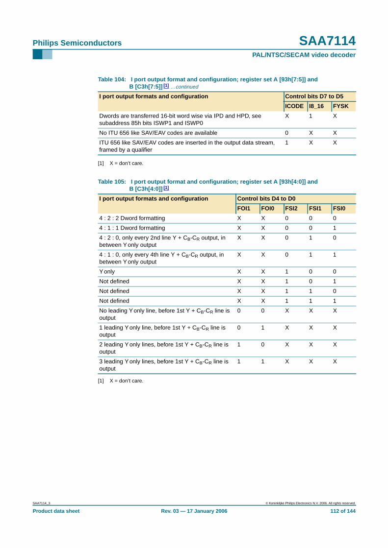
Philips Semiconductors SAA7114PAL/NTSC/SECAM video decoder
[1] X = don’t care.
[1] X = don’t care.
Dwords are transferred 16-bit word wise via IPD and HPD, seesubaddress 85h bits ISWP1 and ISWP0
X 1 X
No ITU 656 like SAV/EAV codes are available 0 X X
ITU 656 like SAV/EAV codes are inserted in the output data stream,framed by a qualifier
1 X X
Table 105: I port output format and configuration; register set A [93h[4:0]] andB [C3h[4:0]] [1]
I port output formats and configuration Control bits D4 to D0
FOI1 FOI0 FSI2 FSI1 FSI0
4 : 2 : 2 Dword formatting X X 0 0 0
4 : 1 : 1 Dword formatting X X 0 0 1
4 : 2 : 0, only every 2nd line Y + CB-CR output, inbetween Yonly output
X X 0 1 0
4 : 1 : 0, only every 4th line Y + CB-CR output, inbetween Yonly output
X X 0 1 1
Yonly X X 1 0 0
Not defined X X 1 0 1
Not defined X X 1 1 0
Not defined X X 1 1 1
No leading Yonly line, before 1st Y + CB-CR line isoutput
0 0 X X X
1 leading Y only line, before 1st Y + CB-CR line isoutput
0 1 X X X
2 leading Y only lines, before 1st Y + CB-CR line isoutput
1 0 X X X
3 leading Y only lines, before 1st Y + CB-CR line isoutput
1 1 X X X
Table 104: I port output format and configuration; register set A [93h[7:5]] andB [C3h[7:5]] [1] …continued
I port output formats and configuration Control bits D7 to D5
ICODE I8_16 FYSK
SAA7114_3 © Koninklijke Philips Electronics N.V. 2006. All rights reserved.
Product data sheet Rev. 03 — 17 January 2006 112 of 144
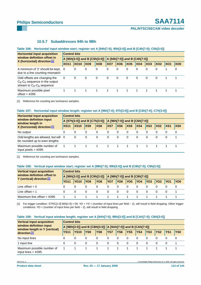
Philips Semiconductors SAA7114PAL/NTSC/SECAM video decoder
10.5.7 Subaddresses 94h to 9Bh
[1] Reference for counting are luminance samples.
[1] Reference for counting are luminance samples.
[1] For trigger condition: STRC[1:0] 90h[1:0] = 00; YO + YS > (number of input lines per field − 2), will result in field dropping. Other triggerconditions: YO > (number of input lines per field − 2), will result in field dropping.
Table 106: Horizontal input window start; register set A [94h[7:0]; 95h[3:0]] and B [C4h[7:0]; C5h[3:0]]
Horizontal input acquisitionwindow definition offset inX (horizontal) direction [1]
Control bits
A [95h[3:0]] and B [C5h[3:0]] A [94h[7:0]] and B [C4h[7:0]]
XO11 XO10 XO9 XO8 XO7 XO6 XO5 XO4 XO3 XO2 XO1 XO0
A minimum of ‘2’ should be kept,due to a line counting mismatch
0 0 0 0 0 0 0 0 0 0 1 0
Odd offsets are changing theCB-CR sequence in the outputstream to CR-CB sequence
0 0 0 0 0 0 0 0 0 0 1 1
Maximum possible pixeloffset = 4095
1 1 1 1 1 1 1 1 1 1 1 1
Table 107: Horizontal input window length; register set A [96h[7:0]; 97h[3:0]] and B [C6h[7:0]; C7h[3:0]]
Horizontal input acquisitionwindow definition inputwindow length inX (horizontal) direction [1]
Control bits
A [97h[3:0]] and B [C7h[3:0]] A [96h[7:0]] and B [C6h[7:0]]
XS11 XS10 XS9 XS8 XS7 XS6 XS5 XS4 XS3 XS2 XS1 XS0
No output 0 0 0 0 0 0 0 0 0 0 0 0
Odd lengths are allowed, but willbe rounded up to even lengths
0 0 0 0 0 0 0 0 0 0 0 1
Maximum possible number ofinput pixels = 4095
1 1 1 1 1 1 1 1 1 1 1 1
Table 108: Vertical input window start; register set A [98h[7:0]; 99h[3:0]] and B [C8h[7:0]; C9h[3:0]]
Vertical input acquisitionwindow definition offset inY (vertical) direction [1]
Control bits
A [99h[3:0]] and B [C9h[3:0]] A [98h[7:0]] and B [C8h[7:0]]
YO11 YO10 YO9 YO8 YO7 YO6 YO5 YO4 YO3 YO2 YO1 YO0
Line offset = 0 0 0 0 0 0 0 0 0 0 0 0 0
Line offset = 1 0 0 0 0 0 0 0 0 0 0 0 1
Maximum line offset = 4095 1 1 1 1 1 1 1 1 1 1 1 1
Table 109: Vertical input window length; register set A [9Ah[7:0]; 9Bh[3:0]] and B [CAh[7:0]; CBh[3:0]]
Vertical input acquisitionwindow definition inputwindow length in Y (vertical)direction [1]
Control bits
A [9Bh[3:0]] and B [CBh[3:0]] A [9Ah[7:0]] and B [CAh[7:0]]
YS11 YS10 YS9 YS8 YS7 YS6 YS5 YS4 YS3 YS2 YS1 YS0
No input lines 0 0 0 0 0 0 0 0 0 0 0 0
1 input line 0 0 0 0 0 0 0 0 0 0 0 1
Maximum possible number ofinput lines = 4095
1 1 1 1 1 1 1 1 1 1 1 1
SAA7114_3 © Koninklijke Philips Electronics N.V. 2006. All rights reserved.
Product data sheet Rev. 03 — 17 January 2006 113 of 144
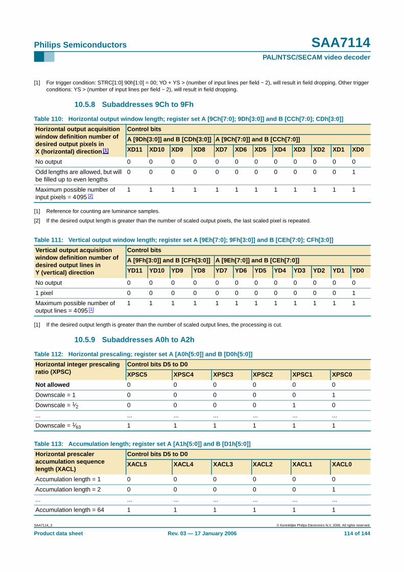
Philips Semiconductors SAA7114PAL/NTSC/SECAM video decoder
[1] For trigger condition: STRC[1:0] 90h[1:0] = 00; YO + YS > (number of input lines per field − 2), will result in field dropping. Other triggerconditions: YS > (number of input lines per field − 2), will result in field dropping.
10.5.8 Subaddresses 9Ch to 9Fh
[1] Reference for counting are luminance samples.
[2] If the desired output length is greater than the number of scaled output pixels, the last scaled pixel is repeated.
[1] If the desired output length is greater than the number of scaled output lines, the processing is cut.
10.5.9 Subaddresses A0h to A2h
Table 110: Horizontal output window length; register set A [9Ch[7:0]; 9Dh[3:0]] and B [CCh[7:0]; CDh[3:0]]
Horizontal output acquisitionwindow definition number ofdesired output pixels inX (horizontal) direction [1]
Control bits
A [9Dh[3:0]] and B [CDh[3:0]] A [9Ch[7:0]] and B [CCh[7:0]]
XD11 XD10 XD9 XD8 XD7 XD6 XD5 XD4 XD3 XD2 XD1 XD0
No output 0 0 0 0 0 0 0 0 0 0 0 0
Odd lengths are allowed, but willbe filled up to even lengths
0 0 0 0 0 0 0 0 0 0 0 1
Maximum possible number ofinput pixels = 4095 [2]
1 1 1 1 1 1 1 1 1 1 1 1
Table 111: Vertical output window length; register set A [9Eh[7:0]; 9Fh[3:0]] and B [CEh[7:0]; CFh[3:0]]
Vertical output acquisitionwindow definition number ofdesired output lines inY (vertical) direction
Control bits
A [9Fh[3:0]] and B [CFh[3:0]] A [9Eh[7:0]] and B [CEh[7:0]]
YD11 YD10 YD9 YD8 YD7 YD6 YD5 YD4 YD3 YD2 YD1 YD0
No output 0 0 0 0 0 0 0 0 0 0 0 0
1 pixel 0 0 0 0 0 0 0 0 0 0 0 1
Maximum possible number ofoutput lines = 4095 [1]
1 1 1 1 1 1 1 1 1 1 1 1
Table 112: Horizontal prescaling; register set A [A0h[5:0]] and B [D0h[5:0]]
Horizontal integer prescalingratio (XPSC)
Control bits D5 to D0
XPSC5 XPSC4 XPSC3 XPSC2 XPSC1 XPSC0
Not allowed 0 0 0 0 0 0
Downscale = 1 0 0 0 0 0 1
Downscale = 1⁄2 0 0 0 0 1 0
... ... ... ... ... ... ...
Downscale = 1⁄63 1 1 1 1 1 1
Table 113: Accumulation length; register set A [A1h[5:0]] and B [D1h[5:0]]
Horizontal prescaleraccumulation sequencelength (XACL)
Control bits D5 to D0
XACL5 XACL4 XACL3 XACL2 XACL1 XACL0
Accumulation length = 1 0 0 0 0 0 0
Accumulation length = 2 0 0 0 0 0 1
... ... ... ... ... ... ...
Accumulation length = 64 1 1 1 1 1 1
SAA7114_3 © Koninklijke Philips Electronics N.V. 2006. All rights reserved.
Product data sheet Rev. 03 — 17 January 2006 114 of 144
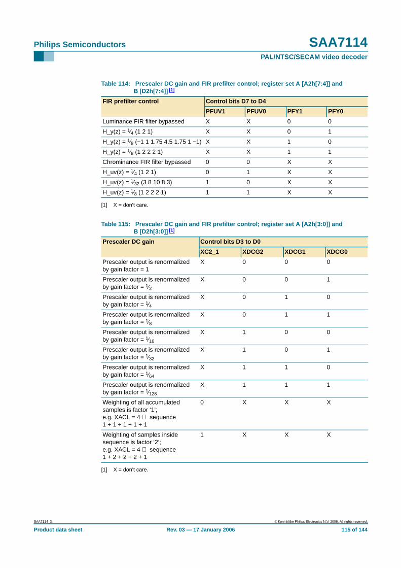
Philips Semiconductors SAA7114PAL/NTSC/SECAM video decoder
[1] X = don’t care.
[1] X = don’t care.
Table 114: Prescaler DC gain and FIR prefilter control; register set A [A2h[7:4]] andB [D2h[7:4]] [1]
FIR prefilter control Control bits D7 to D4
PFUV1 PFUV0 PFY1 PFY0
Luminance FIR filter bypassed X X 0 0
H_y(z) = 1⁄4 (1 2 1) X X 0 1
H_y(z) = 1⁄8 (−1 1 1.75 4.5 1.75 1 −1) X X 1 0
H_y(z) = 1⁄8 (1 2 2 2 1) X X 1 1
Chrominance FIR filter bypassed 0 0 X X
H_uv(z) = 1⁄4 (1 2 1) 0 1 X X
H_uv(z) = 1⁄32 (3 8 10 8 3) 1 0 X X
H_uv(z) = 1⁄8 (1 2 2 2 1) 1 1 X X
Table 115: Prescaler DC gain and FIR prefilter control; register set A [A2h[3:0]] andB [D2h[3:0]] [1]
Prescaler DC gain Control bits D3 to D0
XC2_1 XDCG2 XDCG1 XDCG0
Prescaler output is renormalizedby gain factor = 1
X 0 0 0
Prescaler output is renormalizedby gain factor = 1⁄2
X 0 0 1
Prescaler output is renormalizedby gain factor = 1⁄4
X 0 1 0
Prescaler output is renormalizedby gain factor = 1⁄8
X 0 1 1
Prescaler output is renormalizedby gain factor = 1⁄16
X 1 0 0
Prescaler output is renormalizedby gain factor = 1⁄32
X 1 0 1
Prescaler output is renormalizedby gain factor = 1⁄64
X 1 1 0
Prescaler output is renormalizedby gain factor = 1⁄128
X 1 1 1
Weighting of all accumulatedsamples is factor ‘1’;e.g. XACL = 4 ⇒ sequence1 + 1 + 1 + 1 + 1
0 X X X
Weighting of samples insidesequence is factor ‘2’;e.g. XACL = 4 ⇒ sequence1 + 2 + 2 + 2 + 1
1 X X X
SAA7114_3 © Koninklijke Philips Electronics N.V. 2006. All rights reserved.
Product data sheet Rev. 03 — 17 January 2006 115 of 144
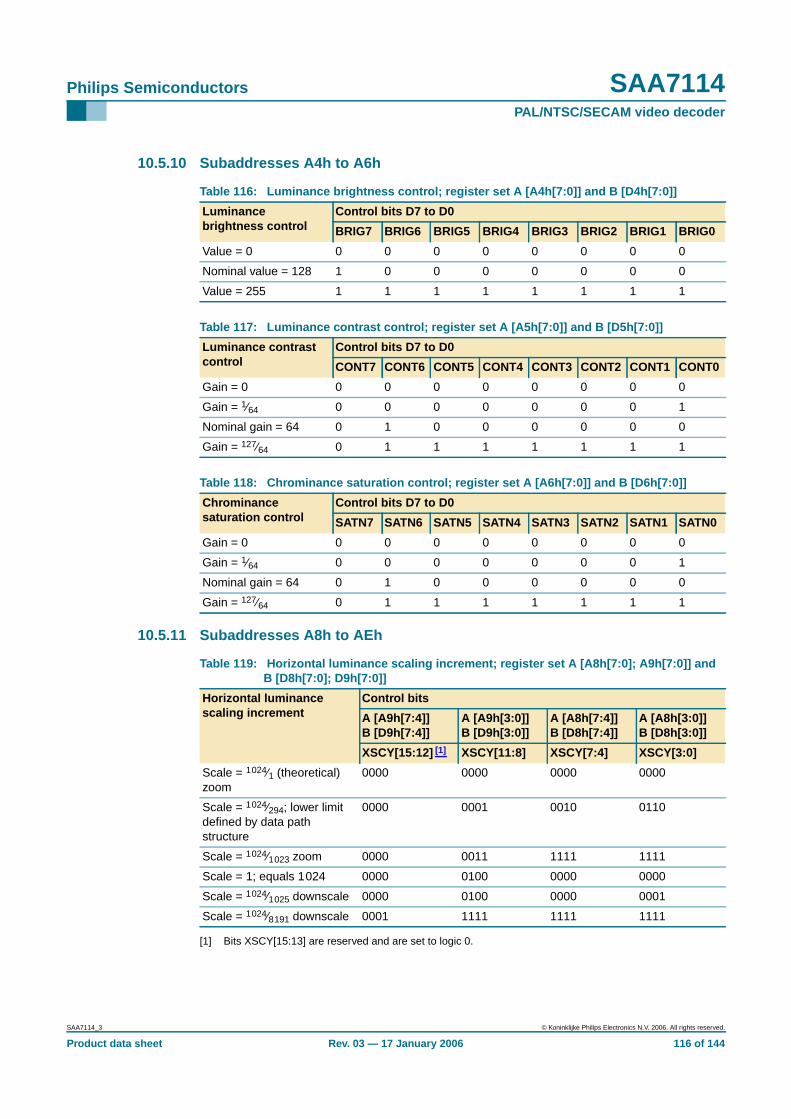
Philips Semiconductors SAA7114PAL/NTSC/SECAM video decoder
10.5.10 Subaddresses A4h to A6h
10.5.11 Subaddresses A8h to AEh
[1] Bits XSCY[15:13] are reserved and are set to logic 0.
Table 116: Luminance brightness control; register set A [A4h[7:0]] and B [D4h[7:0]]
Luminancebrightness control
Control bits D7 to D0
BRIG7 BRIG6 BRIG5 BRIG4 BRIG3 BRIG2 BRIG1 BRIG0
Value = 0 0 0 0 0 0 0 0 0
Nominal value = 128 1 0 0 0 0 0 0 0
Value = 255 1 1 1 1 1 1 1 1
Table 117: Luminance contrast control; register set A [A5h[7:0]] and B [D5h[7:0]]
Luminance contrastcontrol
Control bits D7 to D0
CONT7 CONT6 CONT5 CONT4 CONT3 CONT2 CONT1 CONT0
Gain = 0 0 0 0 0 0 0 0 0
Gain = 1⁄64 0 0 0 0 0 0 0 1
Nominal gain = 64 0 1 0 0 0 0 0 0
Gain = 127⁄64 0 1 1 1 1 1 1 1
Table 118: Chrominance saturation control; register set A [A6h[7:0]] and B [D6h[7:0]]
Chrominancesaturation control
Control bits D7 to D0
SATN7 SATN6 SATN5 SATN4 SATN3 SATN2 SATN1 SATN0
Gain = 0 0 0 0 0 0 0 0 0
Gain = 1⁄64 0 0 0 0 0 0 0 1
Nominal gain = 64 0 1 0 0 0 0 0 0
Gain = 127⁄64 0 1 1 1 1 1 1 1
Table 119: Horizontal luminance scaling increment; register set A [A8h[7:0]; A9h[7:0]] andB [D8h[7:0]; D9h[7:0]]
Horizontal luminancescaling increment
Control bits
A [A9h[7:4]]B [D9h[7:4]]
A [A9h[3:0]]B [D9h[3:0]]
A [A8h[7:4]]B [D8h[7:4]]
A [A8h[3:0]]B [D8h[3:0]]
XSCY[15:12] [1] XSCY[11:8] XSCY[7:4] XSCY[3:0]
Scale = 1024⁄1 (theoretical)zoom
0000 0000 0000 0000
Scale = 1024⁄294; lower limitdefined by data pathstructure
0000 0001 0010 0110
Scale = 1024⁄1023 zoom 0000 0011 1111 1111
Scale = 1; equals 1024 0000 0100 0000 0000
Scale = 1024⁄1025 downscale 0000 0100 0000 0001
Scale = 1024⁄8191 downscale 0001 1111 1111 1111
SAA7114_3 © Koninklijke Philips Electronics N.V. 2006. All rights reserved.
Product data sheet Rev. 03 — 17 January 2006 116 of 144
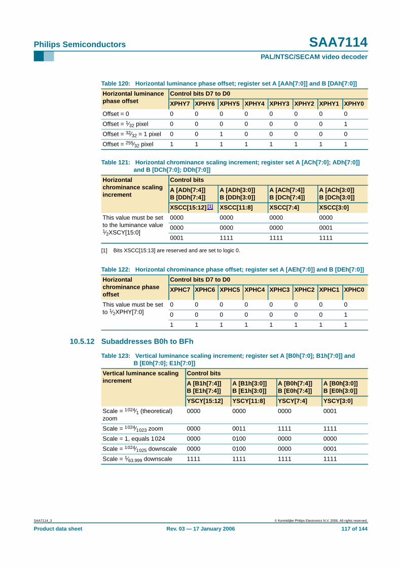
Philips Semiconductors SAA7114PAL/NTSC/SECAM video decoder
[1] Bits XSCC[15:13] are reserved and are set to logic 0.
10.5.12 Subaddresses B0h to BFh
Table 120: Horizontal luminance phase offset; register set A [AAh[7:0]] and B [DAh[7:0]]
Horizontal luminancephase offset
Control bits D7 to D0
XPHY7 XPHY6 XPHY5 XPHY4 XPHY3 XPHY2 XPHY1 XPHY0
Offset = 0 0 0 0 0 0 0 0 0
Offset = 1⁄32 pixel 0 0 0 0 0 0 0 1
Offset = 32⁄32 = 1 pixel 0 0 1 0 0 0 0 0
Offset = 255⁄32 pixel 1 1 1 1 1 1 1 1
Table 121: Horizontal chrominance scaling increment; register set A [ACh[7:0]; ADh[7:0]]and B [DCh[7:0]; DDh[7:0]]
Horizontalchrominance scalingincrement
Control bits
A [ADh[7:4]]B [DDh[7:4]]
A [ADh[3:0]]B [DDh[3:0]]
A [ACh[7:4]]B [DCh[7:4]]
A [ACh[3:0]]B [DCh[3:0]]
XSCC[15:12] [1] XSCC[11:8] XSCC[7:4] XSCC[3:0]
This value must be setto the luminance value1⁄2XSCY[15:0]
0000 0000 0000 0000
0000 0000 0000 0001
0001 1111 1111 1111
Table 122: Horizontal chrominance phase offset; register set A [AEh[7:0]] and B [DEh[7:0]]
Horizontalchrominance phaseoffset
Control bits D7 to D0
XPHC7 XPHC6 XPHC5 XPHC4 XPHC3 XPHC2 XPHC1 XPHC0
This value must be setto 1⁄2XPHY[7:0]
0 0 0 0 0 0 0 0
0 0 0 0 0 0 0 1
1 1 1 1 1 1 1 1
Table 123: Vertical luminance scaling increment; register set A [B0h[7:0]; B1h[7:0]] andB [E0h[7:0]; E1h[7:0]]
Vertical luminance scalingincrement
Control bits
A [B1h[7:4]]B [E1h[7:4]]
A [B1h[3:0]]B [E1h[3:0]]
A [B0h[7:4]]B [E0h[7:4]]
A [B0h[3:0]]B [E0h[3:0]]
YSCY[15:12] YSCY[11:8] YSCY[7:4] YSCY[3:0]
Scale = 1024⁄1 (theoretical)zoom
0000 0000 0000 0001
Scale = 1024⁄1023 zoom 0000 0011 1111 1111
Scale = 1, equals 1024 0000 0100 0000 0000
Scale = 1024⁄1025 downscale 0000 0100 0000 0001
Scale = 1⁄63.999 downscale 1111 1111 1111 1111
SAA7114_3 © Koninklijke Philips Electronics N.V. 2006. All rights reserved.
Product data sheet Rev. 03 — 17 January 2006 117 of 144
Philips Semiconductors SAA7114PAL/NTSC/SECAM video decoder
[1] X = don’t care.
Table 124: Vertical chrominance scaling increment; register set A [B2h[7:0]; B3h[7:0]] andB [E2h[7:0]; E3h[7:0]]
Vertical chrominancescaling increment
Control bits
A [B3h[7:4]]B [E3h[7:4]]
A [B3h[3:0]]B [E3h[3:0]]
A [B2h[7:4]]B [E2h[7:4]]
A [B2h[3:0]]B [E2h[3:0]]
YSCC[15:12] YSCC[11:8] YSCC[7:4] YSCC[3:0]
This value must be setto the luminance valueYSCY[15:0]
0000 0000 0000 0001
1111 1111 1111 1111
Table 125: Vertical scaling mode control; register set A [B4h[4 and 0]] andB [E4h[4 and 0]] [1]
Vertical scaling mode control Control bits D4 and D0
YMIR YMODE
Vertical scaling performs linear interpolation between lines X 0
Vertical scaling performs higher order accumulating interpolation, betteralias suppression
X 1
No mirroring 0 X
Lines are mirrored 1 X
Table 126: Vertical chrominance phase offset ‘00’; register set A [B8h[7:0]] and B [E8h[7:0]]
Vertical chrominancephase offset
Control bits D7 to D0
YPC07 YPC06 YPC05 YPC04 YPC03 YPC02 YPC01 YPC00
Offset = 0 0 0 0 0 0 0 0 0
Offset = 32⁄32 = 1 line 0 0 1 0 0 0 0 0
Offset = 255⁄32 lines 1 1 1 1 1 1 1 1
Table 127: Vertical luminance phase offset ‘00’; register set A [BCh[7:0]] and B [ECh[7:0]]
Vertical luminancephase offset
Control bits D7 to D0
YPY07 YPY06 YPY05 YPY04 YPY03 YPY02 YPY01 YPY00
Offset = 0 0 0 0 0 0 0 0 0
Offset = 32⁄32 = 1 line 0 0 1 0 0 0 0 0
Offset = 255⁄32 lines 1 1 1 1 1 1 1 1
SAA7114_3 © Koninklijke Philips Electronics N.V. 2006. All rights reserved.
Product data sheet Rev. 03 — 17 January 2006 118 of 144
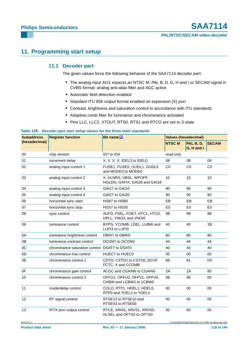
Philips Semiconductors SAA7114PAL/NTSC/SECAM video decoder
11. Programming start setup
11.1 Decoder partThe given values force the following behavior of the SAA7114 decoder part:
• The analog input AI11 expects an NTSC M, PAL B, D, G, H and I or SECAM signal inCVBS format; analog anti-alias filter and AGC active
• Automatic field detection enabled
• Standard ITU 656 output format enabled on expansion (X) port
• Contrast, brightness and saturation control in accordance with ITU standards
• Adaptive comb filter for luminance and chrominance activated
• Pins LLC, LLC2, XTOUT, RTS0, RTS1 and RTCO are set to 3-state
Table 128: Decoder part start setup values for the three main standards
Subaddress(hexadecimal)
Register function Bit name [1] Values (hexadecimal)
NTSC M PAL B, D,G, H and I
SECAM
00 chip version ID7 to ID4 read only
01 increment delay X, X, X, X, IDEL3 to IDEL0 08 08 08
02 analog input control 1 FUSE1, FUSE0, GUDL1, GUDL0and MODE3 to MODE0
C0 C0 C0
03 analog input control 2 X, HLNRS, VBSL, WPOFF,HOLDG, GAFIX, GAI28 and GAI18
10 10 10
04 analog input control 3 GAI17 to GAI10 90 90 90
05 analog input control 4 GAI27 to GAI20 90 90 90
06 horizontal sync start HSB7 to HSB0 EB EB EB
07 horizontal sync stop HSS7 to HSS0 E0 E0 E0
08 sync control AUFD, FSEL, FOET, HTC1, HTC0,HPLL, VNOI1 and VNOI0
98 98 98
09 luminance control BYPS, YCOMB, LDEL, LUBW andLUFI3 to LUFI0
40 40 1B
0A luminance brightness control DBRI7 to DBRI0 80 80 80
0B luminance contrast control DCON7 to DCON0 44 44 44
0C chrominance saturation control DSAT7 to DSAT0 40 40 40
0D chrominance hue control HUEC7 to HUEC0 00 00 00
0E chrominance control 1 CDTO, CSTD2 to CSTD0, DCVF,FCTC, X and CCOMB
89 81 D0
0F chrominance gain control ACGC and CGAIN6 to CGAIN0 2A 2A 80
10 chrominance control 2 OFFU1, OFFU0, OFFV1, OFFV0,CHBW and LCBW2 to LCBW0
0E 06 00
11 mode/delay control COLO, RTP1, HDEL1, HDEL0,RTP0 and YDEL2 to YDEL0
00 00 00
12 RT signal control RTSE13 to RTSE10 andRTSE03 to RTSE00
00 00 00
13 RT/X port output control RTCE, XRHS, XRVS1, XRVS0,HLSEL and OFTS2 to OFTS0
00 00 00
SAA7114_3 © Koninklijke Philips Electronics N.V. 2006. All rights reserved.
Product data sheet Rev. 03 — 17 January 2006 119 of 144
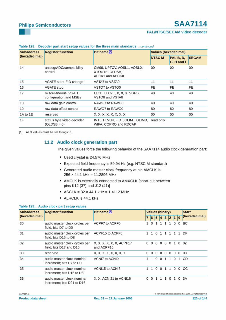
Philips Semiconductors SAA7114PAL/NTSC/SECAM video decoder
[1] All X values must be set to logic 0.
11.2 Audio clock generation partThe given values force the following behavior of the SAA7114 audio clock generation part:
• Used crystal is 24.576 MHz
• Expected field frequency is 59.94 Hz (e.g. NTSC M standard)
• Generated audio master clock frequency at pin AMCLK is256 × 44.1 kHz = 11.2896 MHz
• AMCLK is externally connected to AMXCLK [short-cut betweenpins K12 (37) and J12 (41)]
• ASCLK = 32 × 44.1 kHz = 1.4112 MHz
• ALRCLK is 44.1 kHz
14 analog/ADC/compatibilitycontrol
CM99, UPTCV, AOSL1, AOSL0,XTOUTE, OLDSB,APCK1 and APCK0
00 00 00
15 VGATE start, FID change VSTA7 to VSTA0 11 11 11
16 VGATE stop VSTO7 to VSTO0 FE FE FE
17 miscellaneous, VGATEconfiguration and MSBs
LLCE, LLC2E, X, X, X, VGPS,VSTO8 and VSTA8
40 40 40
18 raw data gain control RAWG7 to RAWG0 40 40 40
19 raw data offset control RAWO7 to RAWO0 80 80 80
1A to 1E reserved X, X, X, X, X, X, X, X 00 00 00
1F status byte video decoder(OLDSB = 0)
INTL, HLVLN, FIDT, GLIMT, GLIMB,WIPA, COPRO and RDCAP
read only
Table 128: Decoder part start setup values for the three main standards …continued
Subaddress(hexadecimal)
Register function Bit name [1] Values (hexadecimal)
NTSC M PAL B, D,G, H and I
SECAM
Table 129: Audio clock part setup values
Subaddress(hexadecimal)
Register function Bit name [1] Values (binary) Start(hexadecimal)7 6 5 4 3 2 1 0
30 audio master clock cycles perfield; bits D7 to D0
ACPF7 to ACPF0 1 0 1 1 1 1 0 0 BC
31 audio master clock cycles perfield; bits D15 to D8
ACPF15 to ACPF8 1 1 0 1 1 1 1 1 DF
32 audio master clock cycles perfield; bits D17 and D16
X, X, X, X, X, X, ACPF17and ACPF16
0 0 0 0 0 0 1 0 02
33 reserved X, X, X, X, X, X, X, X 0 0 0 0 0 0 0 0 00
34 audio master clock nominalincrement; bits D7 to D0
ACNI7 to ACNI0 1 1 0 0 1 1 0 1 CD
35 audio master clock nominalincrement; bits D15 to D8
ACNI15 to ACNI8 1 1 0 0 1 1 0 0 CC
36 audio master clock nominalincrement; bits D21 to D16
X, X, ACNI21 to ACNI16 0 0 1 1 1 0 1 0 3A
SAA7114_3 © Koninklijke Philips Electronics N.V. 2006. All rights reserved.
Product data sheet Rev. 03 — 17 January 2006 120 of 144
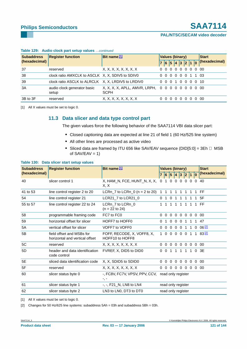
Philips Semiconductors SAA7114PAL/NTSC/SECAM video decoder
[1] All X values must be set to logic 0.
11.3 Data slicer and data type control partThe given values force the following behavior of the SAA7114 VBI data slicer part:
• Closed captioning data are expected at line 21 of field 1 (60 Hz/525 line system)
• All other lines are processed as active video
• Sliced data are framed by ITU 656 like SAV/EAV sequence (DID[5:0] = 3Eh ⇒ MSBof SAV/EAV = 1)
[1] All X values must be set to logic 0.
[2] Changes for 50 Hz/625 line systems: subaddress 5Ah = 03h and subaddress 5Bh = 03h.
37 reserved X, X, X, X, X, X, X, X 0 0 0 0 0 0 0 0 00
38 clock ratio AMXCLK to ASCLK X, X, SDIV5 to SDIV0 0 0 0 0 0 0 1 1 03
39 clock ratio ASCLK to ALRCLK X, X, LRDIV5 to LRDIV0 0 0 0 1 0 0 0 0 10
3A audio clock generator basicsetup
X, X, X, X, APLL, AMVR, LRPH,SCPH
0 0 0 0 0 0 0 0 00
3B to 3F reserved X, X, X, X, X, X, X, X 0 0 0 0 0 0 0 0 00
Table 129: Audio clock part setup values …continued
Subaddress(hexadecimal)
Register function Bit name [1] Values (binary) Start(hexadecimal)7 6 5 4 3 2 1 0
Table 130: Data slicer start setup values
Subaddress(hexadecimal)
Register function Bit name [1] Values (binary) Start(hexadecimal)7 6 5 4 3 2 1 0
40 slicer control 1 X, HAM_N, FCE, HUNT_N, X, X,X, X
0 1 0 0 0 0 0 0 40
41 to 53 line control register 2 to 20 LCRn_7 to LCRn_0 (n = 2 to 20) 1 1 1 1 1 1 1 1 FF
54 line control register 21 LCR21_7 to LCR21_0 0 1 0 1 1 1 1 1 5F
55 to 57 line control register 22 to 24 LCRn_7 to LCRn_0(n = 22 to 24)
1 1 1 1 1 1 1 1 FF
58 programmable framing code FC7 to FC0 0 0 0 0 0 0 0 0 00
59 horizontal offset for slicer HOFF7 to HOFF0 0 1 0 0 0 1 1 1 47
5A vertical offset for slicer VOFF7 to VOFF0 0 0 0 0 0 1 1 0 06 [2]
5B field offset and MSBs forhorizontal and vertical offset
FOFF, RECODE, X, VOFF8, X,HOFF10 to HOFF8
1 0 0 0 0 0 1 1 83 [2]
5C reserved X, X, X, X, X, X, X, X 0 0 0 0 0 0 0 0 00
5D header and data identificationcode control
FVREF, X, DID5 to DID0 0 0 1 1 1 1 1 0 3E
5E sliced data identification code X, X, SDID5 to SDID0 0 0 0 0 0 0 0 0 00
5F reserved X, X, X, X, X, X, X, X 0 0 0 0 0 0 0 0 00
60 slicer status byte 0 -, FC8V, FC7V, VPSV, PPV, CCV,-, -
read only register
61 slicer status byte 1 -, -, F21_N, LN8 to LN4 read only register
62 slicer status byte 2 LN3 to LN0, DT3 to DT0 read only register
SAA7114_3 © Koninklijke Philips Electronics N.V. 2006. All rights reserved.
Product data sheet Rev. 03 — 17 January 2006 121 of 144
Philips Semiconductors SAA7114PAL/NTSC/SECAM video decoder
11.4 Scaler and interfacesTable 131 shows some examples for the scaler programming with:
• prsc = prescale ratio
• fisc = fine scale ratio
• vsc = vertical scale ratio
The ratio is defined as:
In the following settings the VBI data slicer is inactive. To activate the VBI data slicer,VITX[1:0] 86h[7:6] has to be set to ‘11’. Depending on the VBI data slicer settings, thesliced VBI data is inserted after the end of the scaled video lines, if the regions of VBI dataslicer and scaler overlaps.
To compensate the running-in of the vertical scaler, the vertical input window lengths areextended by 2 lines to 290 lines, respectively 242 lines for XS, but the scaler incrementcalculations are done with 288 lines, respectively 240 lines.
11.4.1 Trigger condition
For trigger condition STRC[1:0] 90h[1:0] not equal to ‘00’.
If the value of (YO + YS) is greater than or equal to 262 (NTSC), respectively 312 (PAL)the output field rate is reduced to 30 Hz, respectively 25 Hz.
Horizontal and vertical offsets (XO and YO) have to be used to adjust the displayed videoin the display window. As this adjustment is application dependent, the listed values areonly dummy values.
11.4.2 Maximum zoom factor
The maximum zoom factor is dependent on the back-end data rate and thereforeback-end clock and data format dependent (8-bit or 16-bit output). The maximumhorizontal zoom is limited to approximately 3.5, due to internal data path restrictions.
number of input pixelnumber of output pixel-------------------------------------------------------
SAA7114_3 © Koninklijke Philips Electronics N.V. 2006. All rights reserved.
Product data sheet Rev. 03 — 17 January 2006 122 of 144
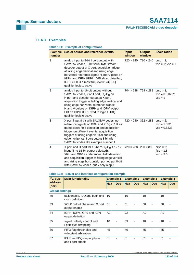
Philips Semiconductors SAA7114PAL/NTSC/SECAM video decoder
11.4.3 Examples
Table 131: Example of configurations
Examplenumber
Scaler source and reference events Inputwindow
Outputwindow
Scale ratios
1 analog input to 8-bit I port output, withSAV/EAV codes, 8-bit serial byte streamdecoder output at X port; acquisition triggerat falling edge vertical and rising edgehorizontal reference signal; H and V gates onIGPH and IGPV, IGP0 = VBI sliced data flag,IGP1 = FIFO almost full, level ≥ 24, IDQqualifier logic 1 active
720 × 240 720 × 240 prsc = 1;fisc = 1; vsc = 1
2 analog input to 16-bit output, withoutSAV/EAV codes, Yon I port, CB-CR onH port and decoder output at X port;acquisition trigger at falling edge vertical andrising edge horizontal reference signal;H and V-pulses on IGPH and IGPV, outputFID on IGP0, IGP1 fixed to logic 1, IDQqualifier logic 0 active
704 × 288 768 × 288 prsc = 1;fisc = 0.91667;vsc = 1
3 X port input 8-bit with SAV/EAV codes, noreference signals on XRH and XRV, XCLK asgated clock; field detection and acquisitiontrigger on different events; acquisitiontriggers at rising edge vertical and risingedge horizontal; I port output 8-bit withSAV/EAV codes like example number 1
720 × 240 352 × 288 prsc = 2;fisc = 1.022;vsc = 0.8333
4 X port and H port for 16-bit Y-CB-CR 4 : 2 : 2input (if no 16-bit output selected);XRH and XRV as references; field detectionand acquisition trigger at falling edge verticaland rising edge horizontal; I port output 8-bitwith SAV/EAV codes, but Yonly output
720 × 288 200 × 80 prsc = 2;fisc = 1.8;vsc = 3.6
Table 132: Scaler and interface configuration example
I2C-busaddress(hex)
Main functionality Example 1 Example 2 Example 3 Example 4
Hex Dec Hex Dec Hex Dec Hex Dec
Global settings
80 task enable, IDQ and back-endclock definition
10 - 10 - 10 - 10 -
83 XCLK output phase and X portoutput enable
01 - 01 - 00 - 00 -
84 IGPH, IGPV, IGP0 and IGP1output definition
A0 - C5 - A0 - A0 -
85 signal polarity control andI port byte swapping
10 - 09 - 10 - 10 -
86 FIFO flag thresholds andvideo/text arbitration
45 - 40 - 45 - 45 -
87 ICLK and IDQ output phaseand I port enable
01 - 01 - 01 - 01 -
SAA7114_3 © Koninklijke Philips Electronics N.V. 2006. All rights reserved.
Product data sheet Rev. 03 — 17 January 2006 123 of 144
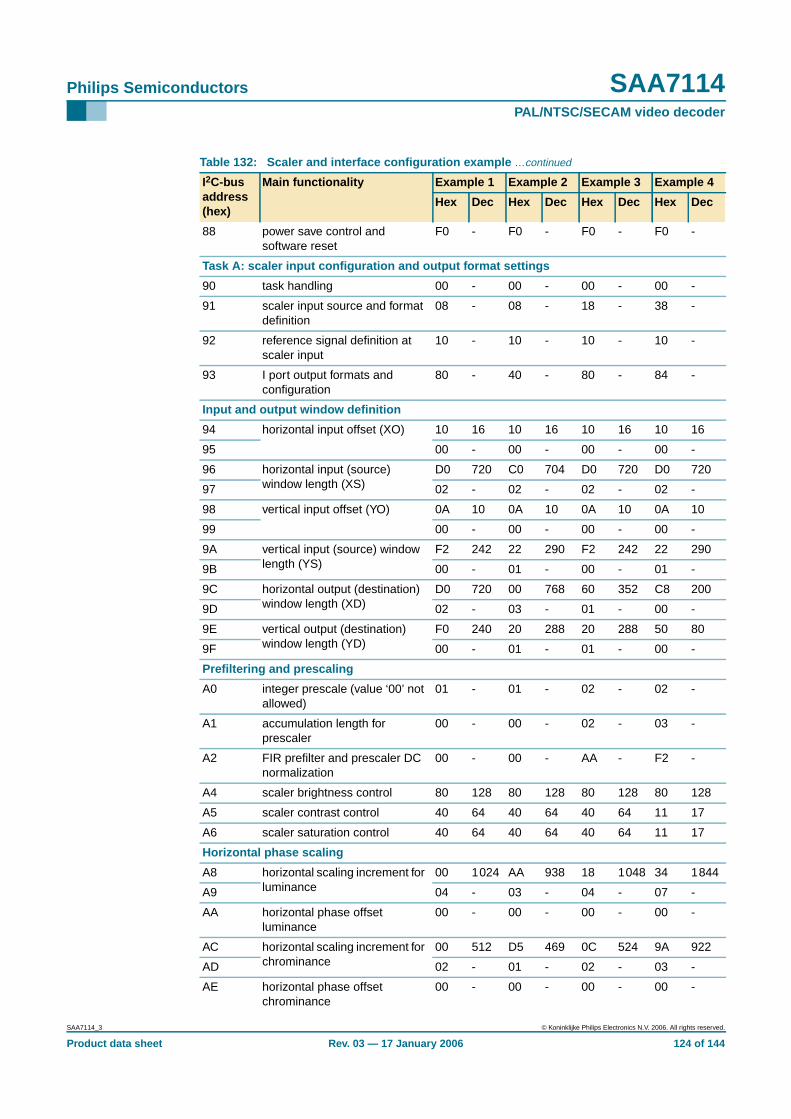
Philips Semiconductors SAA7114PAL/NTSC/SECAM video decoder
88 power save control andsoftware reset
F0 - F0 - F0 - F0 -
Task A: scaler input configuration and output format settings
90 task handling 00 - 00 - 00 - 00 -
91 scaler input source and formatdefinition
08 - 08 - 18 - 38 -
92 reference signal definition atscaler input
10 - 10 - 10 - 10 -
93 I port output formats andconfiguration
80 - 40 - 80 - 84 -
Input and output window definition
94 horizontal input offset (XO) 10 16 10 16 10 16 10 16
95 00 - 00 - 00 - 00 -
96 horizontal input (source)window length (XS)
D0 720 C0 704 D0 720 D0 720
97 02 - 02 - 02 - 02 -
98 vertical input offset (YO) 0A 10 0A 10 0A 10 0A 10
99 00 - 00 - 00 - 00 -
9A vertical input (source) windowlength (YS)
F2 242 22 290 F2 242 22 290
9B 00 - 01 - 00 - 01 -
9C horizontal output (destination)window length (XD)
D0 720 00 768 60 352 C8 200
9D 02 - 03 - 01 - 00 -
9E vertical output (destination)window length (YD)
F0 240 20 288 20 288 50 80
9F 00 - 01 - 01 - 00 -
Prefiltering and prescaling
A0 integer prescale (value ‘00’ notallowed)
01 - 01 - 02 - 02 -
A1 accumulation length forprescaler
00 - 00 - 02 - 03 -
A2 FIR prefilter and prescaler DCnormalization
00 - 00 - AA - F2 -
A4 scaler brightness control 80 128 80 128 80 128 80 128
A5 scaler contrast control 40 64 40 64 40 64 11 17
A6 scaler saturation control 40 64 40 64 40 64 11 17
Horizontal phase scaling
A8 horizontal scaling increment forluminance
00 1024 AA 938 18 1048 34 1844
A9 04 - 03 - 04 - 07 -
AA horizontal phase offsetluminance
00 - 00 - 00 - 00 -
AC horizontal scaling increment forchrominance
00 512 D5 469 0C 524 9A 922
AD 02 - 01 - 02 - 03 -
AE horizontal phase offsetchrominance
00 - 00 - 00 - 00 -
Table 132: Scaler and interface configuration example …continued
I2C-busaddress(hex)
Main functionality Example 1 Example 2 Example 3 Example 4
Hex Dec Hex Dec Hex Dec Hex Dec
SAA7114_3 © Koninklijke Philips Electronics N.V. 2006. All rights reserved.
Product data sheet Rev. 03 — 17 January 2006 124 of 144
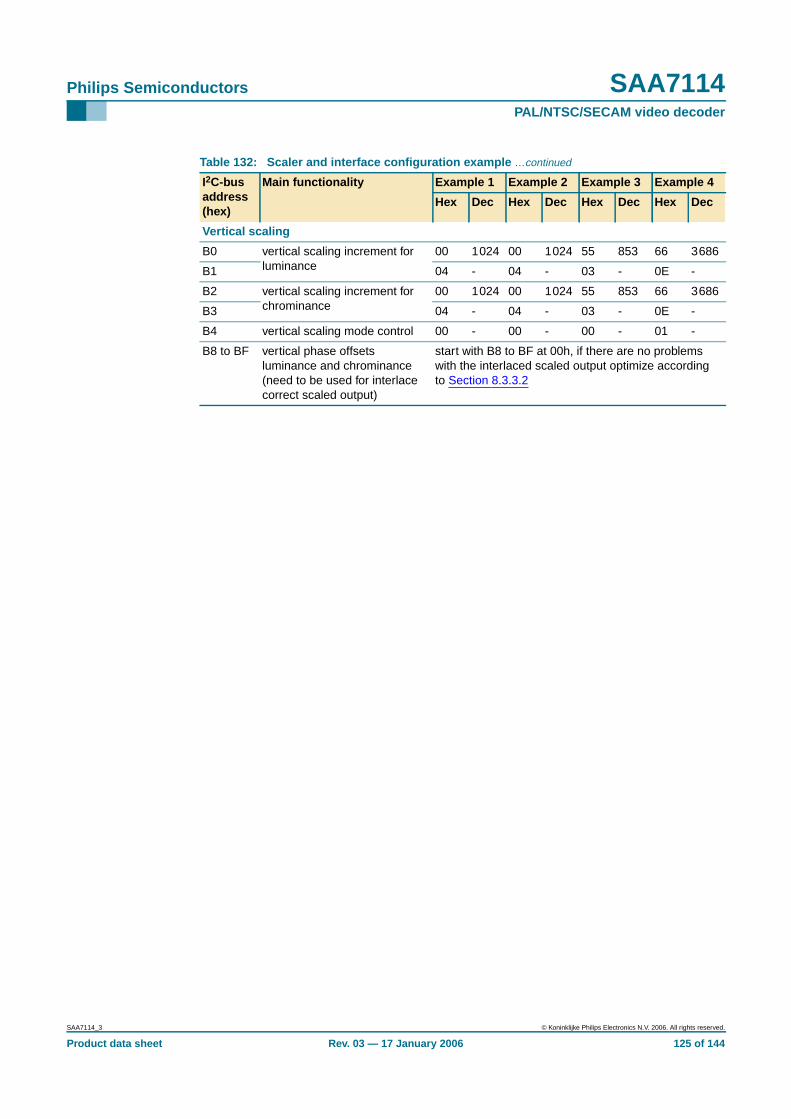
Philips Semiconductors SAA7114PAL/NTSC/SECAM video decoder
Vertical scaling
B0 vertical scaling increment forluminance
00 1024 00 1024 55 853 66 3686
B1 04 - 04 - 03 - 0E -
B2 vertical scaling increment forchrominance
00 1024 00 1024 55 853 66 3686
B3 04 - 04 - 03 - 0E -
B4 vertical scaling mode control 00 - 00 - 00 - 01 -
B8 to BF vertical phase offsetsluminance and chrominance(need to be used for interlacecorrect scaled output)
start with B8 to BF at 00h, if there are no problemswith the interlaced scaled output optimize accordingto Section 8.3.3.2
Table 132: Scaler and interface configuration example …continued
I2C-busaddress(hex)
Main functionality Example 1 Example 2 Example 3 Example 4
Hex Dec Hex Dec Hex Dec Hex Dec
SAA7114_3 © Koninklijke Philips Electronics N.V. 2006. All rights reserved.
Product data sheet Rev. 03 — 17 January 2006 125 of 144
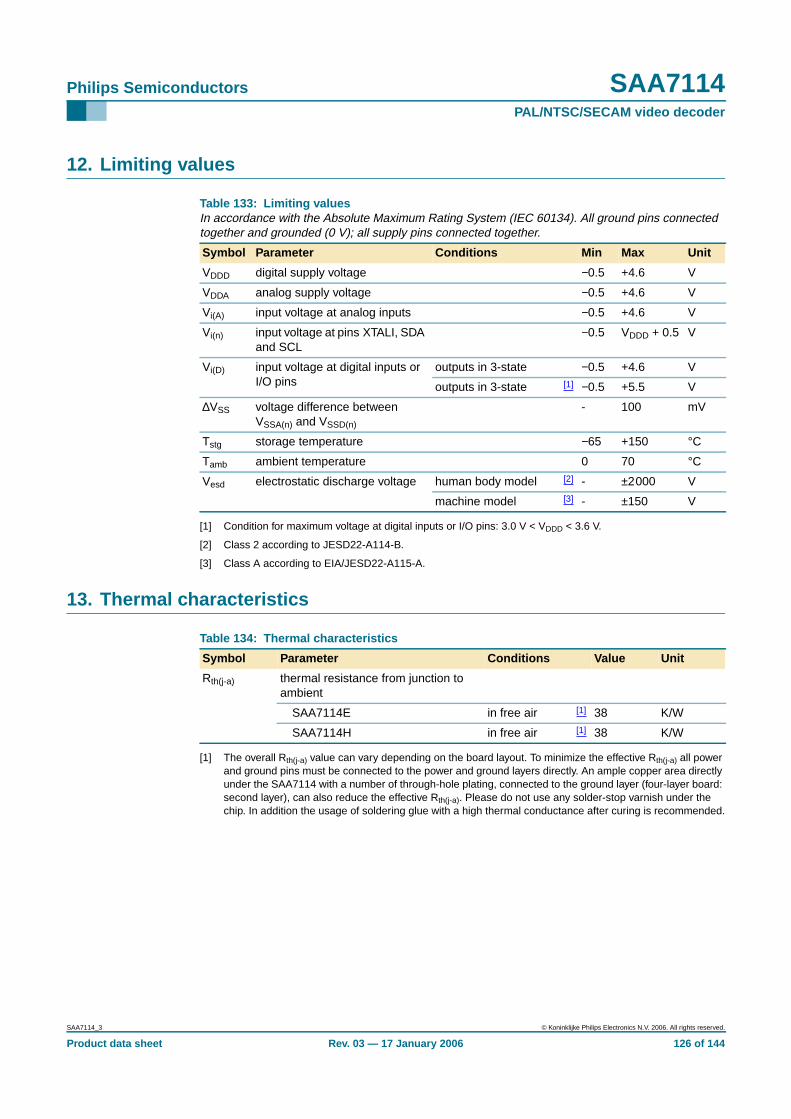
Philips Semiconductors SAA7114PAL/NTSC/SECAM video decoder
12. Limiting values
[1] Condition for maximum voltage at digital inputs or I/O pins: 3.0 V < VDDD < 3.6 V.
[2] Class 2 according to JESD22-A114-B.
[3] Class A according to EIA/JESD22-A115-A.
13. Thermal characteristics
[1] The overall Rth(j-a) value can vary depending on the board layout. To minimize the effective Rth(j-a) all powerand ground pins must be connected to the power and ground layers directly. An ample copper area directlyunder the SAA7114 with a number of through-hole plating, connected to the ground layer (four-layer board:second layer), can also reduce the effective Rth(j-a). Please do not use any solder-stop varnish under thechip. In addition the usage of soldering glue with a high thermal conductance after curing is recommended.
Table 133: Limiting valuesIn accordance with the Absolute Maximum Rating System (IEC 60134). All ground pins connectedtogether and grounded (0 V); all supply pins connected together.
Symbol Parameter Conditions Min Max Unit
VDDD digital supply voltage −0.5 +4.6 V
VDDA analog supply voltage −0.5 +4.6 V
Vi(A) input voltage at analog inputs −0.5 +4.6 V
Vi(n) input voltage at pins XTALI, SDAand SCL
−0.5 VDDD + 0.5 V
Vi(D) input voltage at digital inputs orI/O pins
outputs in 3-state −0.5 +4.6 V
outputs in 3-state [1] −0.5 +5.5 V
∆VSS voltage difference betweenVSSA(n) and VSSD(n)
- 100 mV
Tstg storage temperature −65 +150 °C
Tamb ambient temperature 0 70 °C
Vesd electrostatic discharge voltage human body model [2] - ±2000 V
machine model [3] - ±150 V
Table 134: Thermal characteristics
Symbol Parameter Conditions Value Unit
Rth(j-a) thermal resistance from junction toambient
SAA7114E in free air [1] 38 K/W
SAA7114H in free air [1] 38 K/W
SAA7114_3 © Koninklijke Philips Electronics N.V. 2006. All rights reserved.
Product data sheet Rev. 03 — 17 January 2006 126 of 144
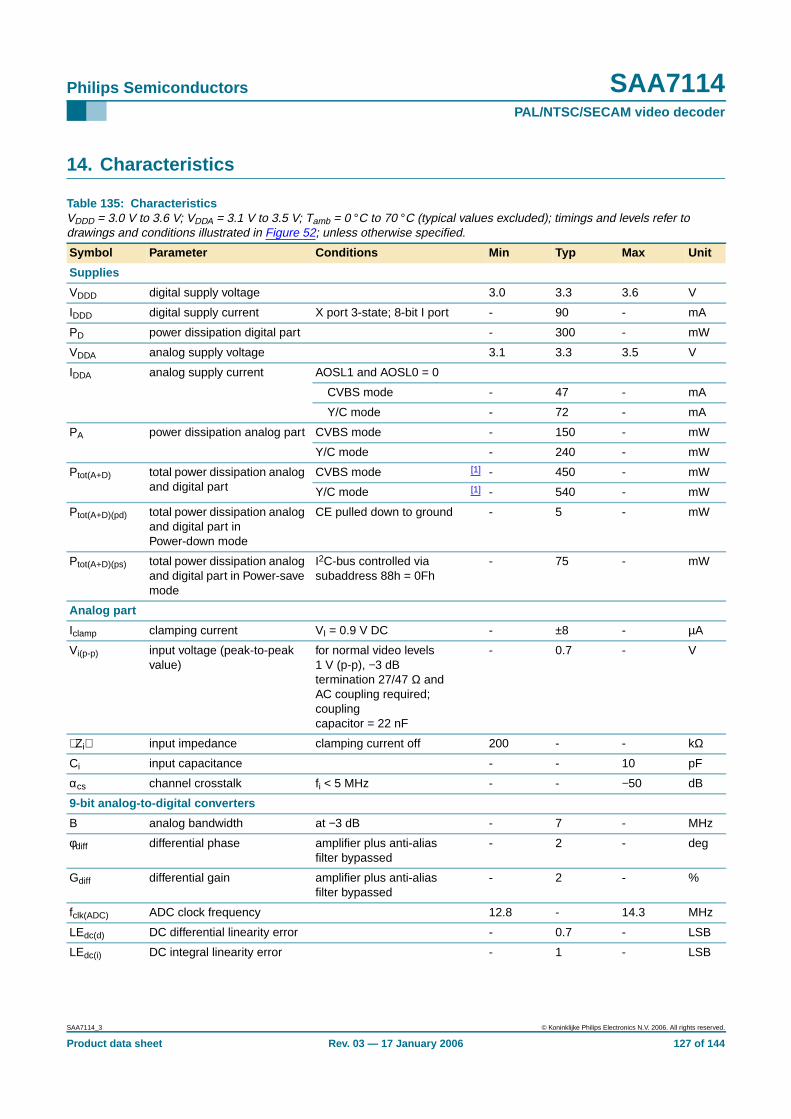
Philips Semiconductors SAA7114PAL/NTSC/SECAM video decoder
14. Characteristics
Table 135: CharacteristicsVDDD = 3.0 V to 3.6 V; VDDA = 3.1 V to 3.5 V; Tamb = 0 °C to 70 °C (typical values excluded); timings and levels refer todrawings and conditions illustrated in Figure 52; unless otherwise specified.
Symbol Parameter Conditions Min Typ Max Unit
Supplies
VDDD digital supply voltage 3.0 3.3 3.6 V
IDDD digital supply current X port 3-state; 8-bit I port - 90 - mA
PD power dissipation digital part - 300 - mW
VDDA analog supply voltage 3.1 3.3 3.5 V
IDDA analog supply current AOSL1 and AOSL0 = 0
CVBS mode - 47 - mA
Y/C mode - 72 - mA
PA power dissipation analog part CVBS mode - 150 - mW
Y/C mode - 240 - mW
Ptot(A+D) total power dissipation analogand digital part
CVBS mode [1] - 450 - mW
Y/C mode [1] - 540 - mW
Ptot(A+D)(pd) total power dissipation analogand digital part inPower-down mode
CE pulled down to ground - 5 - mW
Ptot(A+D)(ps) total power dissipation analogand digital part in Power-savemode
I2C-bus controlled viasubaddress 88h = 0Fh
- 75 - mW
Analog part
Iclamp clamping current VI = 0.9 V DC - ±8 - µA
Vi(p-p) input voltage (peak-to-peakvalue)
for normal video levels1 V (p-p), −3 dBtermination 27/47 Ω andAC coupling required;couplingcapacitor = 22 nF
- 0.7 - V
Zi input impedance clamping current off 200 - - kΩ
Ci input capacitance - - 10 pF
αcs channel crosstalk fi < 5 MHz - - −50 dB
9-bit analog-to-digital converters
B analog bandwidth at −3 dB - 7 - MHz
φdiff differential phase amplifier plus anti-aliasfilter bypassed
- 2 - deg
Gdiff differential gain amplifier plus anti-aliasfilter bypassed
- 2 - %
fclk(ADC) ADC clock frequency 12.8 - 14.3 MHz
LEdc(d) DC differential linearity error - 0.7 - LSB
LEdc(i) DC integral linearity error - 1 - LSB
SAA7114_3 © Koninklijke Philips Electronics N.V. 2006. All rights reserved.
Product data sheet Rev. 03 — 17 January 2006 127 of 144
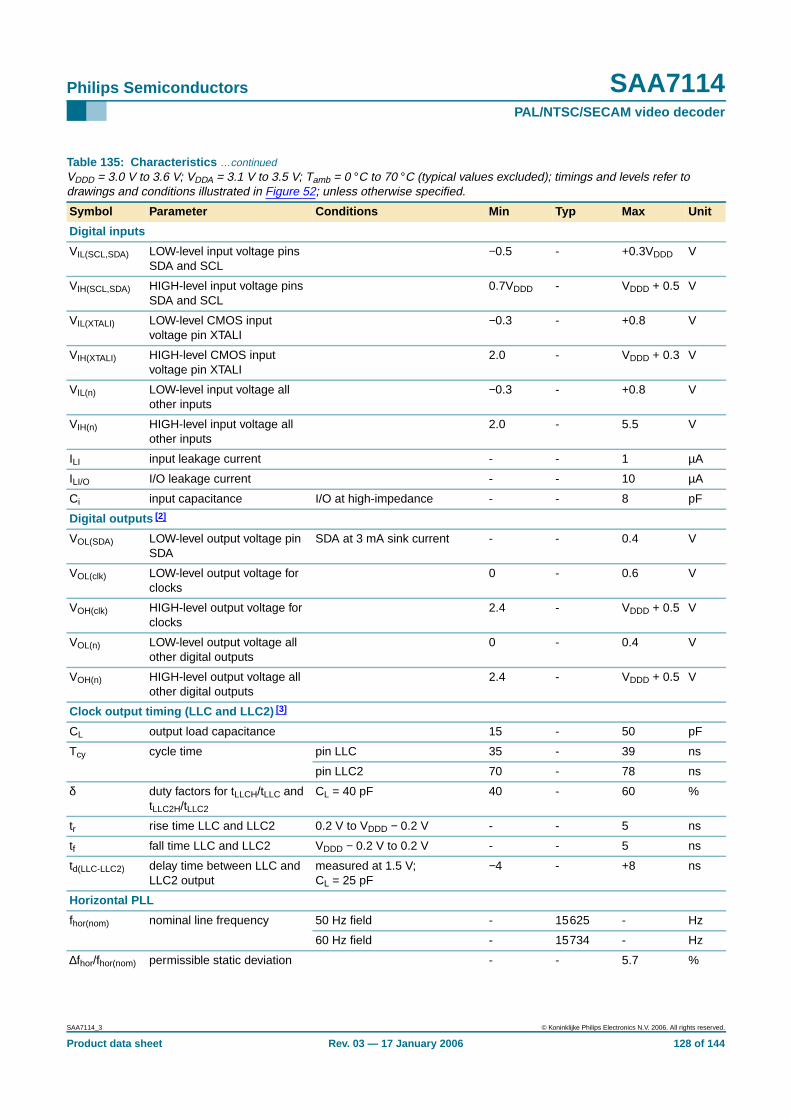
Philips Semiconductors SAA7114PAL/NTSC/SECAM video decoder
Digital inputs
VIL(SCL,SDA) LOW-level input voltage pinsSDA and SCL
−0.5 - +0.3VDDD V
VIH(SCL,SDA) HIGH-level input voltage pinsSDA and SCL
0.7VDDD - VDDD + 0.5 V
VIL(XTALI) LOW-level CMOS inputvoltage pin XTALI
−0.3 - +0.8 V
VIH(XTALI) HIGH-level CMOS inputvoltage pin XTALI
2.0 - VDDD + 0.3 V
VIL(n) LOW-level input voltage allother inputs
−0.3 - +0.8 V
VIH(n) HIGH-level input voltage allother inputs
2.0 - 5.5 V
ILI input leakage current - - 1 µA
ILI/O I/O leakage current - - 10 µA
Ci input capacitance I/O at high-impedance - - 8 pF
Digital outputs [2]
VOL(SDA) LOW-level output voltage pinSDA
SDA at 3 mA sink current - - 0.4 V
VOL(clk) LOW-level output voltage forclocks
0 - 0.6 V
VOH(clk) HIGH-level output voltage forclocks
2.4 - VDDD + 0.5 V
VOL(n) LOW-level output voltage allother digital outputs
0 - 0.4 V
VOH(n) HIGH-level output voltage allother digital outputs
2.4 - VDDD + 0.5 V
Clock output timing (LLC and LLC2) [3]
CL output load capacitance 15 - 50 pF
Tcy cycle time pin LLC 35 - 39 ns
pin LLC2 70 - 78 ns
δ duty factors for tLLCH/tLLC andtLLC2H/tLLC2
CL = 40 pF 40 - 60 %
tr rise time LLC and LLC2 0.2 V to VDDD − 0.2 V - - 5 ns
tf fall time LLC and LLC2 VDDD − 0.2 V to 0.2 V - - 5 ns
td(LLC-LLC2) delay time between LLC andLLC2 output
measured at 1.5 V;CL = 25 pF
−4 - +8 ns
Horizontal PLL
fhor(nom) nominal line frequency 50 Hz field - 15625 - Hz
60 Hz field - 15734 - Hz
∆fhor/fhor(nom) permissible static deviation - - 5.7 %
Table 135: Characteristics …continuedVDDD = 3.0 V to 3.6 V; VDDA = 3.1 V to 3.5 V; Tamb = 0 °C to 70 °C (typical values excluded); timings and levels refer todrawings and conditions illustrated in Figure 52; unless otherwise specified.
Symbol Parameter Conditions Min Typ Max Unit
SAA7114_3 © Koninklijke Philips Electronics N.V. 2006. All rights reserved.
Product data sheet Rev. 03 — 17 January 2006 128 of 144
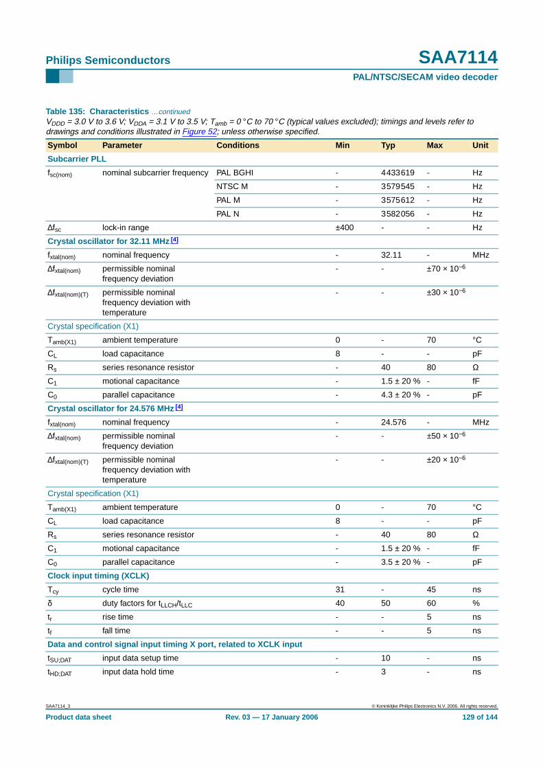
Philips Semiconductors SAA7114PAL/NTSC/SECAM video decoder
Subcarrier PLL
fsc(nom) nominal subcarrier frequency PAL BGHI - 4433619 - Hz
NTSC M - 3579545 - Hz
PAL M - 3575612 - Hz
PAL N - 3582056 - Hz
∆fsc lock-in range ±400 - - Hz
Crystal oscillator for 32.11 MHz [4]
fxtal(nom) nominal frequency - 32.11 - MHz
∆fxtal(nom) permissible nominalfrequency deviation
- - ±70 × 10−6
∆fxtal(nom)(T) permissible nominalfrequency deviation withtemperature
- - ±30 × 10−6
Crystal specification (X1)
Tamb(X1) ambient temperature 0 - 70 °C
CL load capacitance 8 - - pF
Rs series resonance resistor - 40 80 Ω
C1 motional capacitance - 1.5 ± 20 % - fF
C0 parallel capacitance - 4.3 ± 20 % - pF
Crystal oscillator for 24.576 MHz [4]
fxtal(nom) nominal frequency - 24.576 - MHz
∆fxtal(nom) permissible nominalfrequency deviation
- - ±50 × 10−6
∆fxtal(nom)(T) permissible nominalfrequency deviation withtemperature
- - ±20 × 10−6
Crystal specification (X1)
Tamb(X1) ambient temperature 0 - 70 °C
CL load capacitance 8 - - pF
Rs series resonance resistor - 40 80 Ω
C1 motional capacitance - 1.5 ± 20 % - fF
C0 parallel capacitance - 3.5 ± 20 % - pF
Clock input timing (XCLK)
Tcy cycle time 31 - 45 ns
δ duty factors for tLLCH/tLLC 40 50 60 %
tr rise time - - 5 ns
tf fall time - - 5 ns
Data and control signal input timing X port, related to XCLK input
tSU;DAT input data setup time - 10 - ns
tHD;DAT input data hold time - 3 - ns
Table 135: Characteristics …continuedVDDD = 3.0 V to 3.6 V; VDDA = 3.1 V to 3.5 V; Tamb = 0 °C to 70 °C (typical values excluded); timings and levels refer todrawings and conditions illustrated in Figure 52; unless otherwise specified.
Symbol Parameter Conditions Min Typ Max Unit
SAA7114_3 © Koninklijke Philips Electronics N.V. 2006. All rights reserved.
Product data sheet Rev. 03 — 17 January 2006 129 of 144
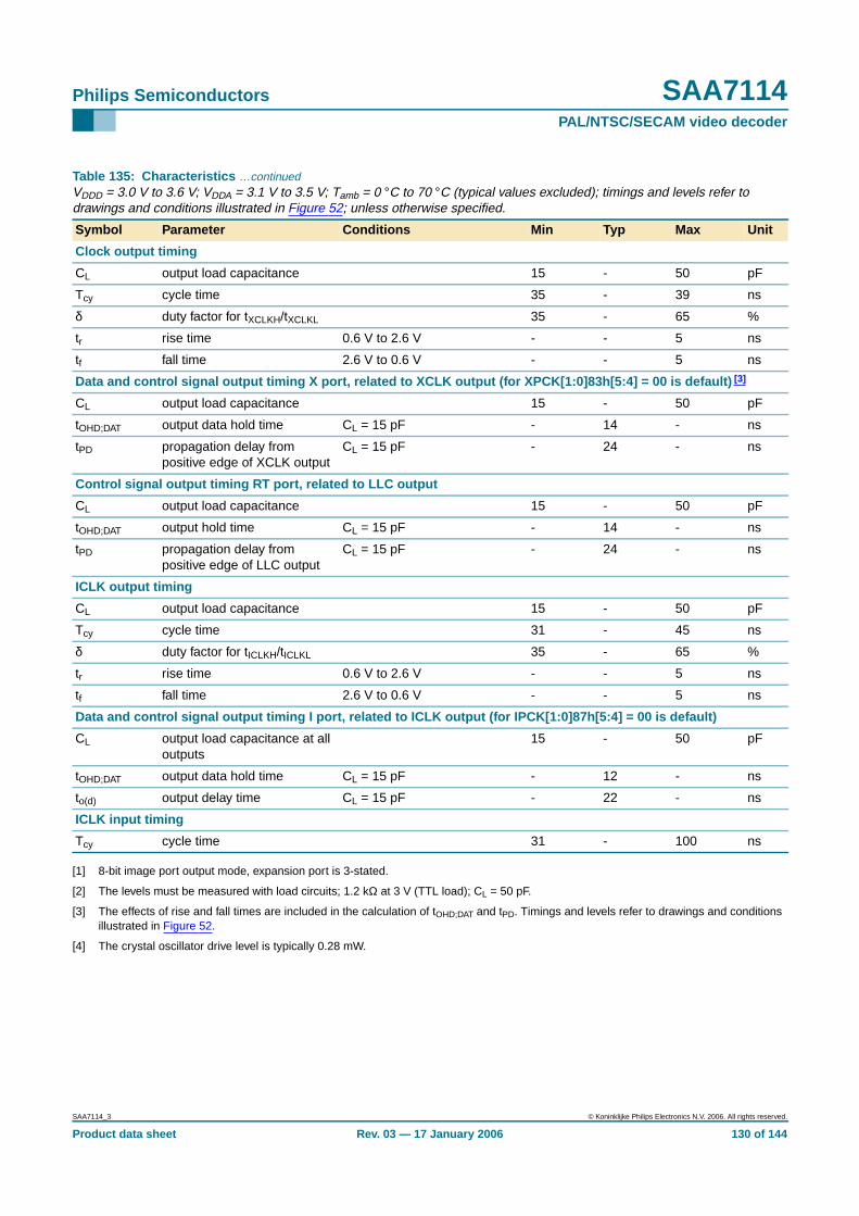
Philips Semiconductors SAA7114PAL/NTSC/SECAM video decoder
[1] 8-bit image port output mode, expansion port is 3-stated.
[2] The levels must be measured with load circuits; 1.2 kΩ at 3 V (TTL load); CL = 50 pF.
[3] The effects of rise and fall times are included in the calculation of tOHD;DAT and tPD. Timings and levels refer to drawings and conditionsillustrated in Figure 52.
[4] The crystal oscillator drive level is typically 0.28 mW.
Clock output timing
CL output load capacitance 15 - 50 pF
Tcy cycle time 35 - 39 ns
δ duty factor for tXCLKH/tXCLKL 35 - 65 %
tr rise time 0.6 V to 2.6 V - - 5 ns
tf fall time 2.6 V to 0.6 V - - 5 ns
Data and control signal output timing X port, related to XCLK output (for XPCK[1:0]83h[5:4] = 00 is default) [3]
CL output load capacitance 15 - 50 pF
tOHD;DAT output data hold time CL = 15 pF - 14 - ns
tPD propagation delay frompositive edge of XCLK output
CL = 15 pF - 24 - ns
Control signal output timing RT port, related to LLC output
CL output load capacitance 15 - 50 pF
tOHD;DAT output hold time CL = 15 pF - 14 - ns
tPD propagation delay frompositive edge of LLC output
CL = 15 pF - 24 - ns
ICLK output timing
CL output load capacitance 15 - 50 pF
Tcy cycle time 31 - 45 ns
δ duty factor for tICLKH/tICLKL 35 - 65 %
tr rise time 0.6 V to 2.6 V - - 5 ns
tf fall time 2.6 V to 0.6 V - - 5 ns
Data and control signal output timing I port, related to ICLK output (for IPCK[1:0]87h[5:4] = 00 is default)
CL output load capacitance at alloutputs
15 - 50 pF
tOHD;DAT output data hold time CL = 15 pF - 12 - ns
to(d) output delay time CL = 15 pF - 22 - ns
ICLK input timing
Tcy cycle time 31 - 100 ns
Table 135: Characteristics …continuedVDDD = 3.0 V to 3.6 V; VDDA = 3.1 V to 3.5 V; Tamb = 0 °C to 70 °C (typical values excluded); timings and levels refer todrawings and conditions illustrated in Figure 52; unless otherwise specified.
Symbol Parameter Conditions Min Typ Max Unit
SAA7114_3 © Koninklijke Philips Electronics N.V. 2006. All rights reserved.
Product data sheet Rev. 03 — 17 January 2006 130 of 144
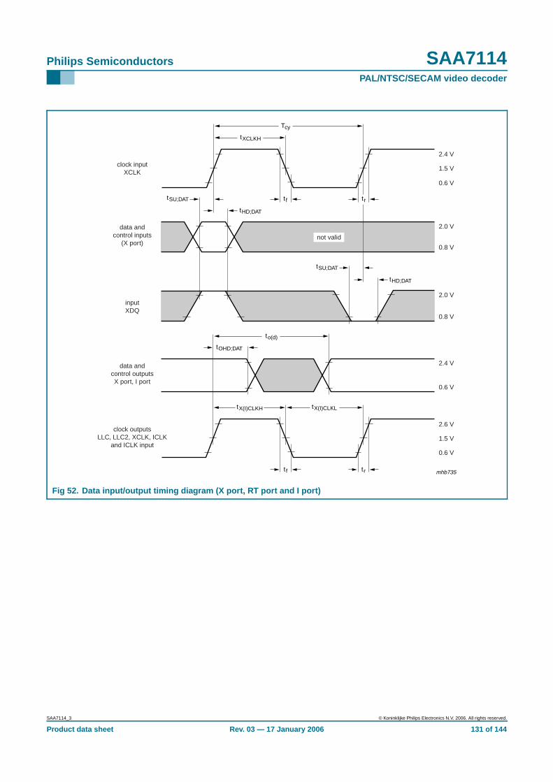
Philips Semiconductors SAA7114PAL/NTSC/SECAM video decoder
Fig 52. Data input/output timing diagram (X port, RT port and I port)
mhb735
tXCLKH
tr
tr
tf
tHD;DAT
tSU;DAT
tSU;DAT
tHD;DAT
Tcy
tX(I)CLKH tX(I)CLKL
tf
clock inputXCLK
data andcontrol inputs
(X port)
data andcontrol outputsX port, I port
clock outputsLLC, LLC2, XCLK, ICLK
and ICLK input
inputXDQ
2.4 V
1.5 V
0.6 V
2.6 V
1.5 V
0.6 V
2.0 V
0.8 V
tOHD;DAT
to(d)
2.4 V
0.6 V
2.0 V
0.8 V
not valid
SAA7114_3 © Koninklijke Philips Electronics N.V. 2006. All rights reserved.
Product data sheet Rev. 03 — 17 January 2006 131 of 144
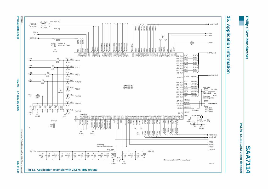
xxxx xxxxxxxxxxxxxxxxxxxxxxxxxxxxxx x xxxxxxxxxxxxxx xxxxxxxxxx xxx xxxxxx xxxxxxxxxxxxxxxxxxxxxxx xxxxxxxxxxxxxxxxxxxxxxxxxxx xxxxxx xx xxxxxxxxxxxxxxxxxxxxxxxxxxxxx xxxxxxxxxxxxxxxxxxxxxx xxxxxxxxxxx xxxxxxx xxxxxxxxxxxxxxxxxxxxxxxxxxxxxxxxxxx xxxxxxxxxxxxxx xxxxxx xx xxxxxxxxxxxxxxxxxxxxxxxxxxxxxxxx xxxxxxxxxxxxxxxxxxxxxxxx xxxxxxxxxxxxxxxxxxxxxxxxxxxxxxxxxxxxxxxxxxxxxxxxxxxxx xxxxxxxxxxx xxxxx x x
SA
A7114_3
Product data shee
Philips S
emiconduc
15.A
pplication in
HPDL[7:0]
TDI
TDO
VDD(3.3)
3.3 V (D)
3.3 V (A)
L2 2.2 µH
L3 2.2 µHVDDA(3.3)
AOUT
SDA
SCL
0 Ω
R17
HP
D5
HP
D6
HP
D7
HP
D0
HP
D1
HP
D2
HP
D3
HP
D4
t
R240 Ω
TP4TP2
TP3
BST2BST[2:0]
Place 0 Ωif BST is not used
T
BS
T0
BS
T1
BS
T2
(XT
AL)
D(E
P1)
D(I
CO
1)
D(I
CO
2)
D(I
CO
3)
D(I
CO
4)
D(I
CO
5)
D(I
CO
6)
A0
A1
A2
D(E
P2)
D(E
P4)
D(E
P3)
5 6 7 T3 TT4
T50 1 2 3 4
torsSA
A7114
PAL/N
TS
C/S
EC
AM
video decoder
formation
FP in parenthesis.
XCON[7:0]
XPD[7:0]
LLC
RTS0
RTS1
RTCO
RESON
mhc614
L110 µH
Y1
DGND
24.576 MHz
C2010 pF
1 nF
C22
C2110 pF
IMCON[7:0]
IPDL[7:0]
R18 0 ΩR21 openR22 open
R15 3.3 kΩ
ACLK
3.3 V (D)
DGND
R20 open
R13 open
Strappingclock frequency
AMCLK
ASCLK
ALRCLK
AMXCLK
XTALO
XTALI
(37) K12
(39) K14
(40) J13
(41) J12
(6) P3
(7)P2
)(4)P4
XT
OU
TX
CO
N6
IGPH
ITRDY
ICLK
IDQ
ITRI
IGP0
IGP1
IGPV
IMCON0
IMCON7
IMCON6
IMCON5
IMCON4
IMCON3
IMCON2
IMCON1
53) G12
(42) J14
(62) B13
61) C13
60) D13
(59) E13
(57) B14
56) C14
55) D14
IPD7
IPD6
IPD5
IPD4
IPD3
IPD2
IPD1
IPD0
IPD6
IPD5
IPD4
IPD3
IPD2
IPD1
IPD0
IPD7(54) E14
45) H12
46) H14
47) G14
(48) F14
49) G13
(52) F13
© K
oninklijke Philips E
lectronics N.V. 2006. A
ll rights reserved.
Rev. 03 —
17 January 2006132 of 144 Fig 53. Application example with 24.576 MHz crystal
C9100nF
C2410 µF
3.3 V (D)
3.3 V (D)
C7100nF
C2100nF
C3100nF
C4100nF
C5100nF
C6100nF
C12100nF
C10100nF
C11100nF
C13100nF
C8100nF
C1100nF
C2310µF
3.3 V (A)
Pin numbers for LQ
R19 open
DGND AGND
AGND AGND
AGND
AGND
AI11
AI12
CE
AI21
AI22
AI23
AI24
R233.3kΩ
0 Ω
R618Ω
R756Ω
R856Ω
R956Ω
R1056Ω
R1156Ω
R1
R1256Ω
R143.3 kΩ
C26P12 (19)
47 nF
C18P11 (18)
47 nF
C25P8 (13)
47 nF
C16
P10 (16)47 nF
C15P9 (14)
47 nF
C14P7 (12)
47 nF
C17P6 (10)
47 nF
C19P13 (20)
AI1D
AI12
AI2D
AI21
AI22
AI23
AI24
AI11
47 nF
R16
18 Ω
R4
18 Ω
R2
18 Ω
R3
18 Ω
R5
18 Ω
DGND
DGND
TP1 TP5
TP6
TP7
StrappingI2C-bus slave address
(92)N2
XR
H
(91)L5
XR
V
(96)N3
XR
DY
(95)M4
XD
Q
(94)M3
XC
LK
(80K1
XT
RI
XC
ON
0
XC
ON
1
XC
ON
2
XC
ON
3
XC
ON
4
XC
ON
5
(81)K2
XP
D7
(82)K3
XP
D6
(84)L1
XP
D5
(85)L2
XP
D4
(86)L3
XP
D3
(87)M1
XP
D2
(89)M2
XP
D1
(90)N1
XP
D0
XP
D7
XP
D6
XP
D5
XP
D4
XP
D3
XP
D2
XP
D1
XP
D0
(36)L13
RT
CO
(35)L10
RT
S1
(34)K13
RT
S0
(44)H13
TE
ST
0
(73)B10
TE
ST
1
(74)C10
TE
ST
2
(28)M14
LLC
(29)L14
LLC
2(30)M12
RE
S
(26)M13
VS
SD
(EP
1)
(100)L6
VS
SD
(EP
2)
(76)H4
VS
SD
(EP
3)
(50)H11
VS
SD
(EP
4)
(5)P5
VS
S(X
TA
L)
(88)K4
VS
SD
(IC
O3)
(63)E11
VS
SD
(IC
O2)
(38)K11
VS
SD
(IC
O1)
(27)N14
CE
(24)N12N13
VS
SA
0
(15)N8N9
VS
SA
1
(9)M7N7
VS
SA
2
(21)N10
AG
ND
(
(
(
(
(
(
(
(
(
M6(98)
M5(99)
N4(97)
N6(3)
N5(2)
TC
K
TM
S
TR
S
TD
I
TD
O
N11(23)
M9(17)
M8(11)
L9(25)
D10(75)
G11(51)
L7(1)
L11(33)
J11(43)
F11(58)
D11(68)
J4(83)
L4(93)
SAA7114E(SAA7114H)
L8(8)
VD
D
VD
D
VD
DV
DD
VD
DV
DD
VD
DV
DD
VD
DV
DD
VD
D
VD
D
VD
D
VD
D
A11(72)
B11(71)
C11(70)
A12(69)
B12(67)
C12(66)
D12(65)
A13(64)
J3(77)
M11(31)
L12(32)
M10(22)
HP
D
HP
D
HP
D
TE
S
SC
L
SD
A
AO
U
J1(78)
J2(79)
TE
S
TE
S
HP
D
HP
D
HP
D
HP
D
HP
D
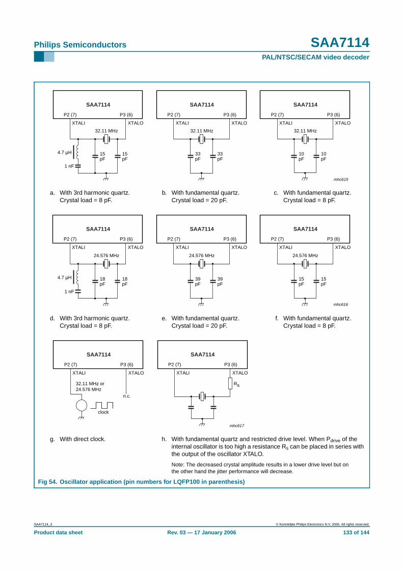
Philips Semiconductors SAA7114PAL/NTSC/SECAM video decoder
a. With 3rd harmonic quartz.Crystal load = 8 pF.
b. With fundamental quartz.Crystal load = 20 pF.
c. With fundamental quartz.Crystal load = 8 pF.
d. With 3rd harmonic quartz.Crystal load = 8 pF.
e. With fundamental quartz.Crystal load = 20 pF.
f. With fundamental quartz.Crystal load = 8 pF.
g. With direct clock. h. With fundamental quartz and restricted drive level. When Pdrive of theinternal oscillator is too high a resistance Rs can be placed in series withthe output of the oscillator XTALO.
Note: The decreased crystal amplitude results in a lower drive level but onthe other hand the jitter performance will decrease.
Fig 54. Oscillator application (pin numbers for LQFP100 in parenthesis)
10pF
10pF
P2 (7)
XTALI
mhc615
XTALO
P3 (6)
32.11 MHz
SAA7114
15pF
1 nF
4.7 µH 15pF
P2 (7)
XTALI XTALO
P3 (6)
32.11 MHz
SAA7114
33pF
33pF
P2 (7)
XTALI XTALO
P3 (6)
32.11 MHz
SAA7114
15pF
15pF
P2 (7)
XTALI XTALO
P3 (6)
24.576 MHz
SAA7114
39pF
39pF
P2 (7)
XTALI XTALO
P3 (6)
24.576 MHz
SAA7114
18pF
1 nF
4.7 µH 18pF
P2 (7)
XTALI XTALO
P3 (6)
24.576 MHz
SAA7114
mhc616
P2 (7)
XTALI XTALO
Rs
P3 (6)
SAA7114
P2 (7)
XTALI XTALO
n.c.
clock
32.11 MHz or24.576 MHz
P3 (6)
SAA7114
mhc617
SAA7114_3 © Koninklijke Philips Electronics N.V. 2006. All rights reserved.
Product data sheet Rev. 03 — 17 January 2006 133 of 144
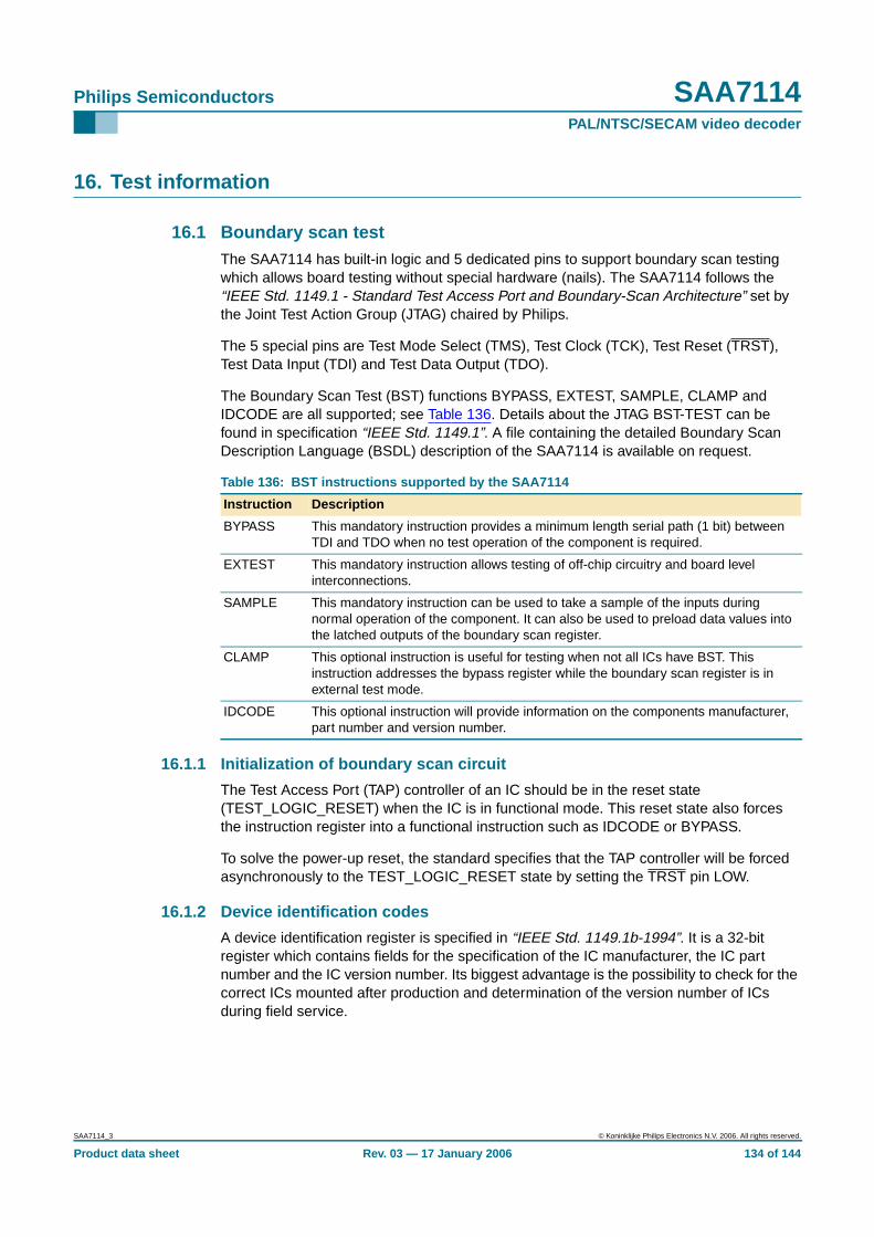
Philips Semiconductors SAA7114PAL/NTSC/SECAM video decoder
16. Test information
16.1 Boundary scan testThe SAA7114 has built-in logic and 5 dedicated pins to support boundary scan testingwhich allows board testing without special hardware (nails). The SAA7114 follows the“IEEE Std. 1149.1 - Standard Test Access Port and Boundary-Scan Architecture” set bythe Joint Test Action Group (JTAG) chaired by Philips.
The 5 special pins are Test Mode Select (TMS), Test Clock (TCK), Test Reset (TRST),Test Data Input (TDI) and Test Data Output (TDO).
The Boundary Scan Test (BST) functions BYPASS, EXTEST, SAMPLE, CLAMP andIDCODE are all supported; see Table 136. Details about the JTAG BST-TEST can befound in specification “IEEE Std. 1149.1”. A file containing the detailed Boundary ScanDescription Language (BSDL) description of the SAA7114 is available on request.
16.1.1 Initialization of boundary scan circuit
The Test Access Port (TAP) controller of an IC should be in the reset state(TEST_LOGIC_RESET) when the IC is in functional mode. This reset state also forcesthe instruction register into a functional instruction such as IDCODE or BYPASS.
To solve the power-up reset, the standard specifies that the TAP controller will be forcedasynchronously to the TEST_LOGIC_RESET state by setting the TRST pin LOW.
16.1.2 Device identification codes
A device identification register is specified in “IEEE Std. 1149.1b-1994”. It is a 32-bitregister which contains fields for the specification of the IC manufacturer, the IC partnumber and the IC version number. Its biggest advantage is the possibility to check for thecorrect ICs mounted after production and determination of the version number of ICsduring field service.
Table 136: BST instructions supported by the SAA7114
Instruction Description
BYPASS This mandatory instruction provides a minimum length serial path (1 bit) betweenTDI and TDO when no test operation of the component is required.
EXTEST This mandatory instruction allows testing of off-chip circuitry and board levelinterconnections.
SAMPLE This mandatory instruction can be used to take a sample of the inputs duringnormal operation of the component. It can also be used to preload data values intothe latched outputs of the boundary scan register.
CLAMP This optional instruction is useful for testing when not all ICs have BST. Thisinstruction addresses the bypass register while the boundary scan register is inexternal test mode.
IDCODE This optional instruction will provide information on the components manufacturer,part number and version number.
SAA7114_3 © Koninklijke Philips Electronics N.V. 2006. All rights reserved.
Product data sheet Rev. 03 — 17 January 2006 134 of 144
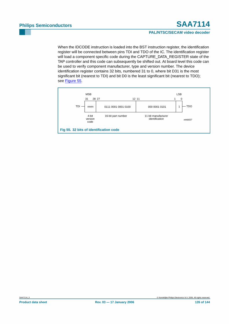
Philips Semiconductors SAA7114PAL/NTSC/SECAM video decoder
When the IDCODE instruction is loaded into the BST instruction register, the identificationregister will be connected between pins TDI and TDO of the IC. The identification registerwill load a component specific code during the CAPTURE_DATA_REGISTER state of theTAP controller and this code can subsequently be shifted out. At board level this code canbe used to verify component manufacturer, type and version number. The deviceidentification register contains 32 bits, numbered 31 to 0, where bit D31 is the mostsignificant bit (nearest to TDI) and bit D0 is the least significant bit (nearest to TDO);see Figure 55.
Fig 55. 32 bits of identification code
mhb557
000 0001 01010111 0001 0001 0100nnnn
4-bitversioncode
16-bit part number 11-bit manufactureridentification
TDI TDO
31
MSB LSB
28 27 12 11 1 0
1
SAA7114_3 © Koninklijke Philips Electronics N.V. 2006. All rights reserved.
Product data sheet Rev. 03 — 17 January 2006 135 of 144
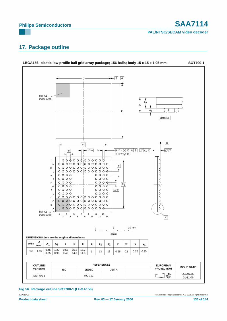
Philips Semiconductors SAA7114PAL/NTSC/SECAM video decoder
17. Package outline
Fig 56. Package outline SOT700-1 (LBGA156)
1
A1 bA2UNIT D ye
REFERENCESOUTLINEVERSION
EUROPEANPROJECTION ISSUE DATE
01-05-1101-11-06
IEC JEDEC JEITA
mm 1.65 0.450.35
1.200.95
15.214.8
y1
15.214.8
e1
13
e2
130.550.45
0.12 0.35
DIMENSIONS (mm are the original dimensions)
SOT700-1 MO-192 - - -- - -
E
0.25
v
0.1
w
0 5 10 mm
scale
SOT700-1LBGA156: plastic low profile ball grid array package; 156 balls; body 15 x 15 x 1.05 mm
Amax.
AA2
A1
detail X
yy1 C
X
D
E
C
B A
A
B
C
D
E
F
H
K
G
J
L
M
N
P
2 4 6 8 10 12 141 3 5 7 9 11 13
ball A1index area
ball A1index area
e
e
e1
b
e2
1/2 e
1/2 e ACC
B∅ v M
∅ w M
SAA7114_3 © Koninklijke Philips Electronics N.V. 2006. All rights reserved.
Product data sheet Rev. 03 — 17 January 2006 136 of 144
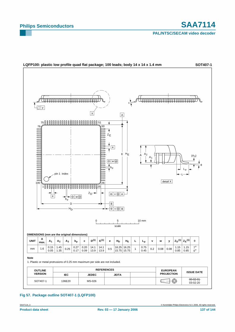
Philips Semiconductors SAA7114PAL/NTSC/SECAM video decoder
Fig 57. Package outline SOT407-1 (LQFP100)
UNITA
max. A1 A2 A3 bp c E(1) e HE L L p Zywv θ
REFERENCESOUTLINEVERSION
EUROPEANPROJECTION ISSUE DATE
IEC JEDEC JEITA
mm 1.6 0.150.05
1.451.35
0.250.270.17
0.200.09
14.113.9
0.516.2515.75
1.150.85
70
o
o0.08 0.080.21
DIMENSIONS (mm are the original dimensions)
Note
1. Plastic or metal protrusions of 0.25 mm maximum per side are not included.
0.750.45
SOT407-1 136E20 MS-02600-02-0103-02-20
D(1) (1)(1)
14.113.9
HD
16.2515.75
EZ
1.150.85
D
bp
e
θ
EA1
A
L p
detail X
L
(A )3
B
25
c
DH
bp
EH A2
v M B
D
ZD
A
ZE
e
v M A
X
1100
7675 51
50
26
y
pin 1 index
w M
w M
0 5 10 mm
scale
LQFP100: plastic low profile quad flat package; 100 leads; body 14 x 14 x 1.4 mm SOT407-1
SAA7114_3 © Koninklijke Philips Electronics N.V. 2006. All rights reserved.
Product data sheet Rev. 03 — 17 January 2006 137 of 144
Philips Semiconductors SAA7114PAL/NTSC/SECAM video decoder
18. Soldering
18.1 Introduction to soldering surface mount packagesThis text gives a very brief insight to a complex technology. A more in-depth account ofsoldering ICs can be found in our Data Handbook IC26; Integrated Circuit Packages(document order number 9398 652 90011).
There is no soldering method that is ideal for all surface mount IC packages. Wavesoldering can still be used for certain surface mount ICs, but it is not suitable for fine pitchSMDs. In these situations reflow soldering is recommended.
18.2 Reflow solderingReflow soldering requires solder paste (a suspension of fine solder particles, flux andbinding agent) to be applied to the printed-circuit board by screen printing, stencilling orpressure-syringe dispensing before package placement. Driven by legislation andenvironmental forces the worldwide use of lead-free solder pastes is increasing.
Several methods exist for reflowing; for example, convection or convection/infraredheating in a conveyor type oven. Throughput times (preheating, soldering and cooling)vary between 100 seconds and 200 seconds depending on heating method.
Typical reflow peak temperatures range from 215 °C to 270 °C depending on solder pastematerial. The top-surface temperature of the packages should preferably be kept:
• below 225 °C (SnPb process) or below 245 °C (Pb-free process)
– for all BGA, HTSSON..T and SSOP..T packages
– for packages with a thickness ≥ 2.5 mm
– for packages with a thickness < 2.5 mm and a volume ≥ 350 mm3 so calledthick/large packages.
• below 240 °C (SnPb process) or below 260 °C (Pb-free process) for packages with athickness < 2.5 mm and a volume < 350 mm3 so called small/thin packages.
Moisture sensitivity precautions, as indicated on packing, must be respected at all times.
18.3 Wave solderingConventional single wave soldering is not recommended for surface mount devices(SMDs) or printed-circuit boards with a high component density, as solder bridging andnon-wetting can present major problems.
To overcome these problems the double-wave soldering method was specificallydeveloped.
If wave soldering is used the following conditions must be observed for optimal results:
• Use a double-wave soldering method comprising a turbulent wave with high upwardpressure followed by a smooth laminar wave.
• For packages with leads on two sides and a pitch (e):
– larger than or equal to 1.27 mm, the footprint longitudinal axis is preferred to beparallel to the transport direction of the printed-circuit board;
SAA7114_3 © Koninklijke Philips Electronics N.V. 2006. All rights reserved.
Product data sheet Rev. 03 — 17 January 2006 138 of 144
Philips Semiconductors SAA7114PAL/NTSC/SECAM video decoder
– smaller than 1.27 mm, the footprint longitudinal axis must be parallel to thetransport direction of the printed-circuit board.
The footprint must incorporate solder thieves at the downstream end.
• For packages with leads on four sides, the footprint must be placed at a 45° angle tothe transport direction of the printed-circuit board. The footprint must incorporatesolder thieves downstream and at the side corners.
During placement and before soldering, the package must be fixed with a droplet ofadhesive. The adhesive can be applied by screen printing, pin transfer or syringedispensing. The package can be soldered after the adhesive is cured.
Typical dwell time of the leads in the wave ranges from 3 seconds to 4 seconds at 250 °Cor 265 °C, depending on solder material applied, SnPb or Pb-free respectively.
A mildly-activated flux will eliminate the need for removal of corrosive residues in mostapplications.
18.4 Manual solderingFix the component by first soldering two diagonally-opposite end leads. Use a low voltage(24 V or less) soldering iron applied to the flat part of the lead. Contact time must belimited to 10 seconds at up to 300 °C.
When using a dedicated tool, all other leads can be soldered in one operation within2 seconds to 5 seconds between 270 °C and 320 °C.
18.5 Package related soldering information
[1] For more detailed information on the BGA packages refer to the (LF)BGA Application Note (AN01026);order a copy from your Philips Semiconductors sales office.
[2] All surface mount (SMD) packages are moisture sensitive. Depending upon the moisture content, themaximum temperature (with respect to time) and body size of the package, there is a risk that internal orexternal package cracks may occur due to vaporization of the moisture in them (the so called popcorneffect). For details, refer to the Drypack information in the Data Handbook IC26; Integrated CircuitPackages; Section: Packing Methods.
[3] These transparent plastic packages are extremely sensitive to reflow soldering conditions and must on noaccount be processed through more than one soldering cycle or subjected to infrared reflow soldering withpeak temperature exceeding 217 °C ± 10 °C measured in the atmosphere of the reflow oven. The packagebody peak temperature must be kept as low as possible.
Table 137: Suitability of surface mount IC packages for wave and reflow soldering methods
Package [1] Soldering method
Wave Reflow [2]
BGA, HTSSON..T [3], LBGA, LFBGA, SQFP,SSOP..T [3], TFBGA, VFBGA, XSON
not suitable suitable
DHVQFN, HBCC, HBGA, HLQFP, HSO, HSOP,HSQFP, HSSON, HTQFP, HTSSOP, HVQFN,HVSON, SMS
not suitable [4] suitable
PLCC [5], SO, SOJ suitable suitable
LQFP, QFP, TQFP not recommended [5] [6] suitable
SSOP, TSSOP, VSO, VSSOP not recommended [7] suitable
CWQCCN..L [8], PMFP [9], WQCCN..L [8] not suitable not suitable
SAA7114_3 © Koninklijke Philips Electronics N.V. 2006. All rights reserved.
Product data sheet Rev. 03 — 17 January 2006 139 of 144
Philips Semiconductors SAA7114PAL/NTSC/SECAM video decoder
[4] These packages are not suitable for wave soldering. On versions with the heatsink on the bottom side, thesolder cannot penetrate between the printed-circuit board and the heatsink. On versions with the heatsinkon the top side, the solder might be deposited on the heatsink surface.
[5] If wave soldering is considered, then the package must be placed at a 45° angle to the solder wavedirection. The package footprint must incorporate solder thieves downstream and at the side corners.
[6] Wave soldering is suitable for LQFP, QFP and TQFP packages with a pitch (e) larger than 0.8 mm; it isdefinitely not suitable for packages with a pitch (e) equal to or smaller than 0.65 mm.
[7] Wave soldering is suitable for SSOP, TSSOP, VSO and VSSOP packages with a pitch (e) equal to or largerthan 0.65 mm; it is definitely not suitable for packages with a pitch (e) equal to or smaller than 0.5 mm.
[8] Image sensor packages in principle should not be soldered. They are mounted in sockets or deliveredpre-mounted on flex foil. However, the image sensor package can be mounted by the client on a flex foil byusing a hot bar soldering process. The appropriate soldering profile can be provided on request.
[9] Hot bar soldering or manual soldering is suitable for PMFP packages.
SAA7114_3 © Koninklijke Philips Electronics N.V. 2006. All rights reserved.
Product data sheet Rev. 03 — 17 January 2006 140 of 144
Philips Semiconductors SAA7114PAL/NTSC/SECAM video decoder
19. Revision history
Table 138: Revision history
Document ID Release date Data sheet status Change notice Doc. number Supersedes
SAA7114_3 20060117 Product data sheet CPCN200505019 - SAA7114_2
Modifications: • The format of this data sheet has been redesigned to comply with the new presentation andinformation standard of Philips Semiconductors
• Table 135: Digital outputs; LOW-level output voltage for clocks corrected from −0.5 V to 0 V
• Package outline changed from SOT472-1 to SOT700-1
SAA7114_2 20040303 Product specification - 9397 750 11429 SAA7114H_1
SAA7114H_1 20000315 Preliminary specification - 9397 750 05976 -
SAA7114_3 © Koninklijke Philips Electronics N.V. 2006. All rights reserved.
Product data sheet Rev. 03 — 17 January 2006 141 of 144
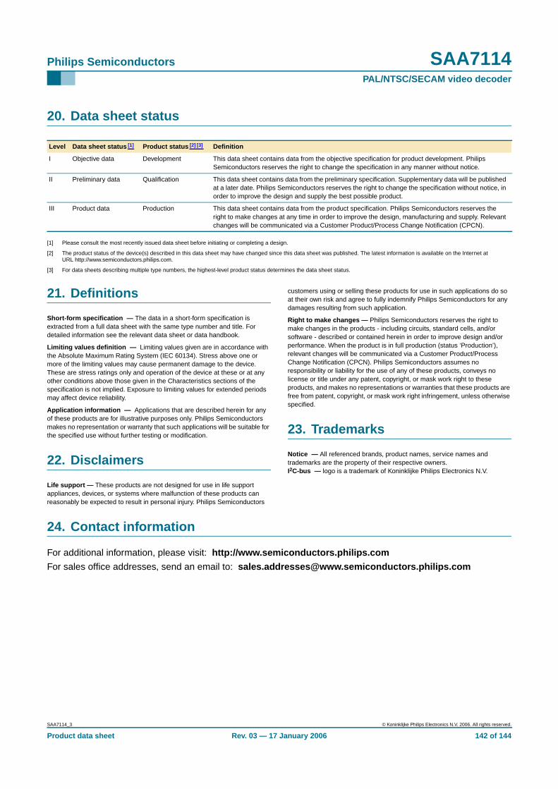
Philips Semiconductors SAA7114PAL/NTSC/SECAM video decoder
20. Data sheet status
[1] Please consult the most recently issued data sheet before initiating or completing a design.
[2] The product status of the device(s) described in this data sheet may have changed since this data sheet was published. The latest information is available on the Internet atURL http://www.semiconductors.philips.com.
[3] For data sheets describing multiple type numbers, the highest-level product status determines the data sheet status.
21. Definitions
Short-form specification — The data in a short-form specification isextracted from a full data sheet with the same type number and title. Fordetailed information see the relevant data sheet or data handbook.
Limiting values definition — Limiting values given are in accordance withthe Absolute Maximum Rating System (IEC 60134). Stress above one ormore of the limiting values may cause permanent damage to the device.These are stress ratings only and operation of the device at these or at anyother conditions above those given in the Characteristics sections of thespecification is not implied. Exposure to limiting values for extended periodsmay affect device reliability.
Application information — Applications that are described herein for anyof these products are for illustrative purposes only. Philips Semiconductorsmakes no representation or warranty that such applications will be suitable forthe specified use without further testing or modification.
22. Disclaimers
Life support — These products are not designed for use in life supportappliances, devices, or systems where malfunction of these products canreasonably be expected to result in personal injury. Philips Semiconductors
customers using or selling these products for use in such applications do soat their own risk and agree to fully indemnify Philips Semiconductors for anydamages resulting from such application.
Right to make changes — Philips Semiconductors reserves the right tomake changes in the products - including circuits, standard cells, and/orsoftware - described or contained herein in order to improve design and/orperformance. When the product is in full production (status ‘Production’),relevant changes will be communicated via a Customer Product/ProcessChange Notification (CPCN). Philips Semiconductors assumes noresponsibility or liability for the use of any of these products, conveys nolicense or title under any patent, copyright, or mask work right to theseproducts, and makes no representations or warranties that these products arefree from patent, copyright, or mask work right infringement, unless otherwisespecified.
23. Trademarks
Notice — All referenced brands, product names, service names andtrademarks are the property of their respective owners.I2C-bus — logo is a trademark of Koninklijke Philips Electronics N.V.
24. Contact information
For additional information, please visit: http://www.semiconductors.philips.com
For sales office addresses, send an email to: [email protected]
Level Data sheet status [1] Product status [2] [3] Definition
I Objective data Development This data sheet contains data from the objective specification for product development. PhilipsSemiconductors reserves the right to change the specification in any manner without notice.
II Preliminary data Qualification This data sheet contains data from the preliminary specification. Supplementary data will be publishedat a later date. Philips Semiconductors reserves the right to change the specification without notice, inorder to improve the design and supply the best possible product.
III Product data Production This data sheet contains data from the product specification. Philips Semiconductors reserves theright to make changes at any time in order to improve the design, manufacturing and supply. Relevantchanges will be communicated via a Customer Product/Process Change Notification (CPCN).
SAA7114_3 © Koninklijke Philips Electronics N.V. 2006. All rights reserved.
Product data sheet Rev. 03 — 17 January 2006 142 of 144
Philips Semiconductors SAA7114PAL/NTSC/SECAM video decoder
25. Contents
1 General description . . . . . . . . . . . . . . . . . . . . . . 12 Features . . . . . . . . . . . . . . . . . . . . . . . . . . . . . . . 22.1 Video decoder. . . . . . . . . . . . . . . . . . . . . . . . . . 22.2 Video scaler . . . . . . . . . . . . . . . . . . . . . . . . . . . 22.3 VBI data decoder and slicer . . . . . . . . . . . . . . . 32.4 Audio clock generation . . . . . . . . . . . . . . . . . . . 32.5 Digital I/O interfaces . . . . . . . . . . . . . . . . . . . . . 32.6 Miscellaneous . . . . . . . . . . . . . . . . . . . . . . . . . . 33 Applications . . . . . . . . . . . . . . . . . . . . . . . . . . . . 34 Quick reference data . . . . . . . . . . . . . . . . . . . . . 45 Ordering information . . . . . . . . . . . . . . . . . . . . . 46 Block diagram . . . . . . . . . . . . . . . . . . . . . . . . . . 57 Pinning information . . . . . . . . . . . . . . . . . . . . . . 67.1 Pinning . . . . . . . . . . . . . . . . . . . . . . . . . . . . . . . 67.2 Pin description . . . . . . . . . . . . . . . . . . . . . . . . . 88 Functional description . . . . . . . . . . . . . . . . . . 148.1 Decoder . . . . . . . . . . . . . . . . . . . . . . . . . . . . . 148.1.1 Analog input processing . . . . . . . . . . . . . . . . . 148.1.2 Analog control circuits. . . . . . . . . . . . . . . . . . . 148.1.2.1 Clamping. . . . . . . . . . . . . . . . . . . . . . . . . . . . . 168.1.2.2 Gain control . . . . . . . . . . . . . . . . . . . . . . . . . . 168.1.3 Chrominance and luminance processing . . . . 198.1.3.1 Chrominance path . . . . . . . . . . . . . . . . . . . . . 208.1.3.2 Luminance path . . . . . . . . . . . . . . . . . . . . . . . 248.1.3.3 Brightness Contrast Saturation (BCS)
control and decoder output levels . . . . . . . . . . 308.1.4 Synchronization . . . . . . . . . . . . . . . . . . . . . . . 318.1.5 Clock generation circuit . . . . . . . . . . . . . . . . . 318.1.6 Power-on reset and CE input . . . . . . . . . . . . . 328.2 Decoder output formatter . . . . . . . . . . . . . . . . 348.3 Scaler . . . . . . . . . . . . . . . . . . . . . . . . . . . . . . . 398.3.1 Acquisition control and task handling
(subaddresses 80h, 90h, 91h, 94h to 9Fh andC4h to CFh) . . . . . . . . . . . . . . . . . . . . . . . . . . 40
8.3.1.1 Input field processing . . . . . . . . . . . . . . . . . . . 418.3.1.2 Task handling . . . . . . . . . . . . . . . . . . . . . . . . . 428.3.1.3 Output field processing . . . . . . . . . . . . . . . . . . 438.3.2 Horizontal scaling . . . . . . . . . . . . . . . . . . . . . . 458.3.2.1 Horizontal prescaler (subaddresses A0h to
A7h and D0h to D7h) . . . . . . . . . . . . . . . . . . . 458.3.2.2 Horizontal fine scaling (variable phase delay
filter; subaddresses A8h to AFh and D8hto DFh) . . . . . . . . . . . . . . . . . . . . . . . . . . . . . . 49
8.3.3 Vertical scaling . . . . . . . . . . . . . . . . . . . . . . . . 508.3.3.1 Line FIFO buffer (subaddresses 91h, B4h
and C1h, E4h). . . . . . . . . . . . . . . . . . . . . . . . . 50
8.3.3.2 Vertical scaler (subaddresses B0h to BFhand E0h to EFh) . . . . . . . . . . . . . . . . . . . . . . . 51
8.3.3.3 Use of the vertical phase offsets . . . . . . . . . . 528.4 VBI data decoder and capture
(subaddresses 40h to 7Fh) . . . . . . . . . . . . . . 548.5 Image port output formatter
(subaddresses 84h to 87h) . . . . . . . . . . . . . . 558.5.1 Scaler output formatter
(subaddresses 93h and C3h). . . . . . . . . . . . . 568.5.2 Video FIFO (subaddress 86h) . . . . . . . . . . . . 578.5.3 Text FIFO . . . . . . . . . . . . . . . . . . . . . . . . . . . . 588.5.4 Video and text arbitration (subaddress 86h) . 588.5.5 Data stream coding and reference signal
generation (subaddresses 84h, 85h and 93h) 588.6 Audio clock generation
(subaddresses 30h to 3Fh) . . . . . . . . . . . . . . 618.6.1 Master audio clock . . . . . . . . . . . . . . . . . . . . . 618.6.2 Signals ASCLK and ALRCLK. . . . . . . . . . . . . 628.6.3 Other control signals . . . . . . . . . . . . . . . . . . . 639 Input/output interfaces and ports . . . . . . . . . 649.1 Analog terminals . . . . . . . . . . . . . . . . . . . . . . 649.2 Audio clock signals. . . . . . . . . . . . . . . . . . . . . 649.3 Clock and real-time synchronization signals . 659.4 Video expansion port (X port) . . . . . . . . . . . . 669.4.1 X port configured as output . . . . . . . . . . . . . . 679.4.2 X port configured as input . . . . . . . . . . . . . . . 709.5 Image port (I port) . . . . . . . . . . . . . . . . . . . . . 709.6 Host port for 16-bit extension of video data
I/O (H port) . . . . . . . . . . . . . . . . . . . . . . . . . . . 729.7 Basic input and output timing diagrams I port
and X port . . . . . . . . . . . . . . . . . . . . . . . . . . . 739.7.1 I port output timing . . . . . . . . . . . . . . . . . . . . . 739.7.2 X port input timing . . . . . . . . . . . . . . . . . . . . . 7310 I2C-bus description . . . . . . . . . . . . . . . . . . . . . 7610.1 I2C-bus format . . . . . . . . . . . . . . . . . . . . . . . . 7610.2 I2C-bus details . . . . . . . . . . . . . . . . . . . . . . . . 8410.2.1 Subaddress 00h . . . . . . . . . . . . . . . . . . . . . . . 8410.2.2 Subaddress 01h . . . . . . . . . . . . . . . . . . . . . . . 8410.2.3 Subaddress 02h . . . . . . . . . . . . . . . . . . . . . . . 8410.2.4 Subaddress 03h . . . . . . . . . . . . . . . . . . . . . . . 8610.2.5 Subaddress 04h . . . . . . . . . . . . . . . . . . . . . . . 8710.2.6 Subaddress 05h . . . . . . . . . . . . . . . . . . . . . . . 8710.2.7 Subaddress 06h . . . . . . . . . . . . . . . . . . . . . . . 8710.2.8 Subaddress 07h . . . . . . . . . . . . . . . . . . . . . . . 8810.2.9 Subaddress 08h . . . . . . . . . . . . . . . . . . . . . . . 8810.2.10 Subaddress 09h . . . . . . . . . . . . . . . . . . . . . . . 8910.2.11 Subaddress 0Ah. . . . . . . . . . . . . . . . . . . . . . . 90
SAA7114_3 © Koninklijke Philips Electronics N.V. 2006. All rights reserved.
Product data sheet Rev. 03 — 17 January 2006 143 of 144
continued >>
Philips Semiconductors SAA7114PAL/NTSC/SECAM video decoder
10.2.12 Subaddress 0Bh . . . . . . . . . . . . . . . . . . . . . . . 9110.2.13 Subaddress 0Ch. . . . . . . . . . . . . . . . . . . . . . . 9110.2.14 Subaddress 0Dh. . . . . . . . . . . . . . . . . . . . . . . 9110.2.15 Subaddress 0Eh . . . . . . . . . . . . . . . . . . . . . . . 9210.2.16 Subaddress 0Fh . . . . . . . . . . . . . . . . . . . . . . . 9310.2.17 Subaddress 10h . . . . . . . . . . . . . . . . . . . . . . . 9310.2.18 Subaddress 11h . . . . . . . . . . . . . . . . . . . . . . . 9310.2.19 Subaddress 12h . . . . . . . . . . . . . . . . . . . . . . . 9410.2.20 Subaddress 13h . . . . . . . . . . . . . . . . . . . . . . . 9610.2.21 Subaddress 14h . . . . . . . . . . . . . . . . . . . . . . . 9710.2.22 Subaddress 15h . . . . . . . . . . . . . . . . . . . . . . . 9710.2.23 Subaddress 16h . . . . . . . . . . . . . . . . . . . . . . . 9810.2.24 Subaddress 17h . . . . . . . . . . . . . . . . . . . . . . . 9810.2.25 Subaddress 18h . . . . . . . . . . . . . . . . . . . . . . . 9810.2.26 Subaddress 19h . . . . . . . . . . . . . . . . . . . . . . . 9910.2.27 Subaddress 1Fh . . . . . . . . . . . . . . . . . . . . . . . 9910.3 Programming register audio clock generation 10010.3.1 Subaddresses 30h to 32h. . . . . . . . . . . . . . . 10010.3.2 Subaddresses 34h to 36h. . . . . . . . . . . . . . . 10010.3.3 Subaddress 38h . . . . . . . . . . . . . . . . . . . . . . 10010.3.4 Subaddress 39h . . . . . . . . . . . . . . . . . . . . . . 10010.3.5 Subaddress 3Ah . . . . . . . . . . . . . . . . . . . . . . 10010.4 Programming register VBI data slicer . . . . . . 10110.4.1 Subaddress 40h . . . . . . . . . . . . . . . . . . . . . . 10110.4.2 Subaddresses 41h to 57h. . . . . . . . . . . . . . . 10110.4.3 Subaddress 58h . . . . . . . . . . . . . . . . . . . . . . 10210.4.4 Subaddress 59h . . . . . . . . . . . . . . . . . . . . . . 10210.4.5 Subaddress 5Ah . . . . . . . . . . . . . . . . . . . . . . 10210.4.6 Subaddress 5Bh . . . . . . . . . . . . . . . . . . . . . . 10210.4.7 Subaddress 5Dh. . . . . . . . . . . . . . . . . . . . . . 10210.4.8 Subaddress 5Eh . . . . . . . . . . . . . . . . . . . . . . 10310.4.9 Subaddress 60h . . . . . . . . . . . . . . . . . . . . . . 10310.4.10 Subaddresses 61h and 62h . . . . . . . . . . . . . 10310.5 Programming register interfaces and scaler
part . . . . . . . . . . . . . . . . . . . . . . . . . . . . . . . . 10310.5.1 Subaddress 80h . . . . . . . . . . . . . . . . . . . . . . 10310.5.2 Subaddresses 83h to 87h. . . . . . . . . . . . . . . 10410.5.3 Subaddress 88h . . . . . . . . . . . . . . . . . . . . . . 10810.5.4 Subaddress 8Fh . . . . . . . . . . . . . . . . . . . . . . 10810.5.5 Subaddresses 90h and C0h . . . . . . . . . . . . . 10910.5.6 Subaddresses 91h to 93h. . . . . . . . . . . . . . . 11010.5.7 Subaddresses 94h to 9Bh . . . . . . . . . . . . . . 11310.5.8 Subaddresses 9Ch to 9Fh . . . . . . . . . . . . . . 11410.5.9 Subaddresses A0h to A2h . . . . . . . . . . . . . . 11410.5.10 Subaddresses A4h to A6h . . . . . . . . . . . . . . 11610.5.11 Subaddresses A8h to AEh . . . . . . . . . . . . . . 11610.5.12 Subaddresses B0h to BFh . . . . . . . . . . . . . . 11711 Programming start setup . . . . . . . . . . . . . . . 11911.1 Decoder part. . . . . . . . . . . . . . . . . . . . . . . . . 11911.2 Audio clock generation part . . . . . . . . . . . . . 120
11.3 Data slicer and data type control part . . . . . 12111.4 Scaler and interfaces . . . . . . . . . . . . . . . . . . 12211.4.1 Trigger condition. . . . . . . . . . . . . . . . . . . . . . 12211.4.2 Maximum zoom factor . . . . . . . . . . . . . . . . . 12211.4.3 Examples . . . . . . . . . . . . . . . . . . . . . . . . . . . 12312 Limiting values . . . . . . . . . . . . . . . . . . . . . . . 12613 Thermal characteristics . . . . . . . . . . . . . . . . 12614 Characteristics . . . . . . . . . . . . . . . . . . . . . . . 12715 Application information . . . . . . . . . . . . . . . . 13216 Test information. . . . . . . . . . . . . . . . . . . . . . . 13416.1 Boundary scan test . . . . . . . . . . . . . . . . . . . 13416.1.1 Initialization of boundary scan circuit . . . . . . 13416.1.2 Device identification codes. . . . . . . . . . . . . . 13417 Package outline . . . . . . . . . . . . . . . . . . . . . . . 13618 Soldering . . . . . . . . . . . . . . . . . . . . . . . . . . . . 13818.1 Introduction to soldering surface mount
packages . . . . . . . . . . . . . . . . . . . . . . . . . . . 13818.2 Reflow soldering. . . . . . . . . . . . . . . . . . . . . . 13818.3 Wave soldering. . . . . . . . . . . . . . . . . . . . . . . 13818.4 Manual soldering . . . . . . . . . . . . . . . . . . . . . 13918.5 Package related soldering information . . . . . 13919 Revision history . . . . . . . . . . . . . . . . . . . . . . 14120 Data sheet status. . . . . . . . . . . . . . . . . . . . . . 14221 Definitions . . . . . . . . . . . . . . . . . . . . . . . . . . . 14222 Disclaimers . . . . . . . . . . . . . . . . . . . . . . . . . . 14223 Trademarks . . . . . . . . . . . . . . . . . . . . . . . . . . 14224 Contact information . . . . . . . . . . . . . . . . . . . 142
© Koninklijke Philips Electronics N.V. 2006All rights are reserved. Reproduction in whole or in part is prohibited without the priorwritten consent of the copyright owner. The information presented in this document doesnot form part of any quotation or contract, is believed to be accurate and reliable and maybe changed without notice. No liability will be accepted by the publisher for anyconsequence of its use. Publication thereof does not convey nor imply any license underpatent- or other industrial or intellectual property rights.
Date of release: 17 January 2006Document number: SAA7114_3
Published in The Netherlands