TTC Interface Module for ATLAS Read-Out Electronics: Final ...
5
TTC Interface Module for ATLAS Read-Out Electronics: Final production version based on Xilinx FPGA devices Jonathan Butterworth, John Lane, Martin Postranecky, Matthew Warren Department of Physics and Astronomy, University College London, Gower Street, London, WC1E 6BT, UK [email protected] Abstract The functionality and the details of the upgraded firmware and hardware of the Xilinx FPGA-based production version of the ATLAS-SCT TTC Interface Module (TIM) are described. The TIM interfaces ATLAS SCT, Pixel, MDT and CSC Read-Out Drivers to the ATLAS Level-1 Trigger using the LHC-standard TTC (Timing, Trigger and Control) and Busy systems. Twelve prototype TIM modules, based on ten AMD/Lattice CPLD devices, have been produced and used since 2001. Final production modules, based on two Xilinx FPGAs, are in manufacture. The details of the transition in hardware and firmware from CPLD to FPGA are described. I. INTRODUCTION The TTC Interface Module (TIM) interfaces the ATLAS Level-1 Trigger system signals to the SCT and Pixel inner sub-detectors, as well as the MDT and CSC muon sub-detector Read-Out Drivers (RODs). Clock and trigger signals are received from the Timing, Trigger and Control (TTC [1]) system and a busy signal is returned to the Central Trigger Processor (CTP). These interfaces can be seen in Figure 1. TTC Interface Module (TIM) Backplane Drivers Backplane Receiver ROD Crate Controller Configuration, Control, Status Clock Fast Commands & Serialised IDs Busy Read Out Drivers (RODs) Standalone Clock + Control ID FIFOs TTCrx Level 1 Trigger TTC/Busy System Optical Signals In VME Slave Interface MRMW/JBL v1.3 16-09-04 Sequencer Busy OR, Mask & Monitor Busy External Inputs Busy Output NIM/ECL Front-panel I/O L1A, BCR, ECR etc. Figure 1: TIM interfaces and main functional blocks. A single TIM distributes the clock and trigger signals to a maximum of 16 RODs with their associated Back-Of- Crate cards (BOCs). Communication is via a custom J3 backplane in a 9U VME64x crate. Each ROD returns an individual busy signal to the TIM, where a crate-busy signal is generated. Figure 2 shows these connections graphically. Signals Busses Front-End Modules Clock & Control (optical) (48/BOC) ROD Busys MRMW v1.1 16-09-04 Clocks Fanout TTC (optical) ROD Crate Busy VM E NIM / ECL Signals ROD Read-Out Driver RCC ROD Crate Controller BOC Back Of Crate TIM TTC Interface Module TIM -OK Figure 2. TIM connections in a ROD-crate. In stand-alone mode the TIM is capable of generating all the TTC-type signals internally under software control. External inputs are also available, these signals being formatted to fit TIM-ROD interface specifications. Twelve prototype TIMs have been produced in the past 3 years. These are being used at various SCT assembly sites, at the SCT and Pixel test-beams and the ROD-DAQ development sites. It has been our aim from the start of the design work to make all versions TIM compatible as far as the end users are concerned. As details of the TIM requirements and operation are detailed in two past papers [2,3], this paper describes only changes to the hardware design and firmware functionality used in the production TIM.
Transcript of TTC Interface Module for ATLAS Read-Out Electronics: Final ...
TTC Interface Module for ATLAS Read-Out Electronics: Final production version based on Xilinx FPGA devices
Jonathan Butterworth, John Lane, Martin Postranecky, Matthew Warren
Department of Physics and Astronomy, University College London, Gower Street, London, WC1E 6BT, UK [email protected]
Abstract The functionality and the details of the upgraded
firmware and hardware of the Xilinx FPGA-based production version of the ATLAS-SCT TTC Interface Module (TIM) are described. The TIM interfaces ATLAS SCT, Pixel, MDT and CSC Read-Out Drivers to the ATLAS Level-1 Trigger using the LHC-standard TTC (Timing, Trigger and Control) and Busy systems. Twelve prototype TIM modules, based on ten AMD/Lattice CPLD devices, have been produced and used since 2001. Final production modules, based on two Xilinx FPGAs, are in manufacture. The details of the transition in hardware and firmware from CPLD to FPGA are described.
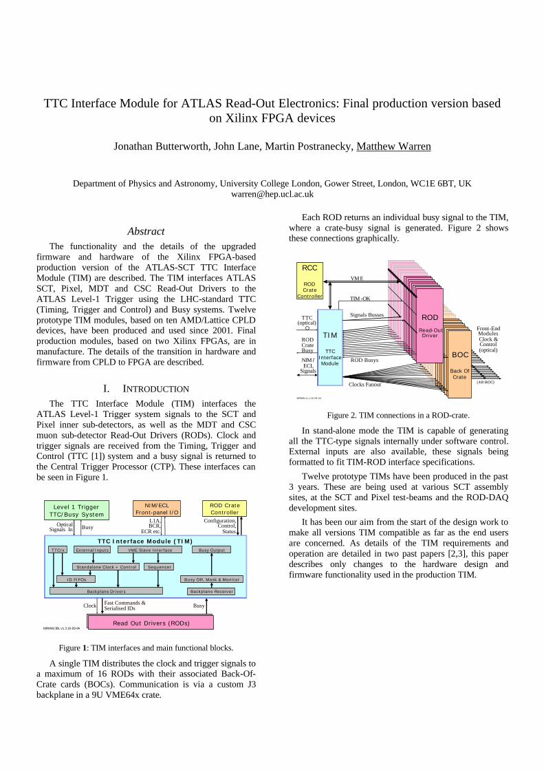
I. INTRODUCTION The TTC Interface Module (TIM) interfaces the
ATLAS Level-1 Trigger system signals to the SCT and Pixel inner sub-detectors, as well as the MDT and CSC muon sub-detector Read-Out Drivers (RODs). Clock and trigger signals are received from the Timing, Trigger and Control (TTC [1]) system and a busy signal is returned to the Central Trigger Processor (CTP). These interfaces can be seen in Figure 1.
TTC Interface Module (TIM)
Backplane Drivers Backplane Receiver
ROD Crate Controller
Configuration, Control,
Status
Read Out Drivers (RODs)
Clock Fast Commands & Serialised IDs Busy
Read Out Drivers (RODs)
Standalone Clock + Control
ID FIFOs
TTCrx
Level 1 Trigger TTC/Busy System
Optical Signals In
VME Slave Interface
MRMW/JBL v1.3 16-09-04
Sequencer
Busy OR, Mask & Monitor
Busy
External Inputs Busy Output
NIM/ECLFront-panel I/O
L1A, BCR,
ECR etc.
Figure 1: TIM interfaces and main functional blocks.
A single TIM distributes the clock and trigger signals to a maximum of 16 RODs with their associated Back-Of-Crate cards (BOCs). Communication is via a custom J3 backplane in a 9U VME64x crate.
Each ROD returns an individual busy signal to the TIM, where a crate-busy signal is generated. Figure 2 shows these connections graphically.
BOCBOCBOCBOCBOCBOCBOCBOCBOCBOCBOCBOCBOCBOCBOC
ROD (Read-Out Drive
r)
ROD (Read-Out Drive
r)
ROD (Read-Out Drive
r)
ROD (Read-Out Drive
r)
ROD (Read-Out Drive
r)
ROD (Read-Out Drive
r)
ROD (Read-Out Drive
r)
RODFP /POResets
ROD (Read-Out Drive
r)
ROD (Read-Out Drive
r)
ROD (Read-Out Drive
r)
ROD (Read-Out Drive
r)
ROD (Read-Out Drive
r)
RODSignals Busses
ROD (Read-Out Drive
r)
Front-End Modules Clock & Control (optical)
(48/BOC)
ROD Busys
MRMW v1.1 16 -09-04
Clocks Fanout
TTC (optical)
ROD Crate Busy
VM E
NIM / ECL
Signals
ROD
Read-Out Driver
RCC
ROD Crate
Controller
BOC
Back Of Crate
TIM
TTC Interface Module
TIM -OK
Figure 2. TIM connections in a ROD-crate.
In stand-alone mode the TIM is capable of generating all the TTC-type signals internally under software control. External inputs are also available, these signals being formatted to fit TIM-ROD interface specifications.
Twelve prototype TIMs have been produced in the past 3 years. These are being used at various SCT assembly sites, at the SCT and Pixel test-beams and the ROD-DAQ development sites.
It has been our aim from the start of the design work to make all versions TIM compatible as far as the end users are concerned. As details of the TIM requirements and operation are detailed in two past papers [2,3], this paper describes only changes to the hardware design and firmware functionality used in the production TIM.

ROD Backplane Mapping & PECL Drivers
J3 Backplane ROD Signals OutputVME Buffers
FPGA1 XC2S200E
(VME Interface)
NIM/ECL Signals I/O
FPGA2 XC2S600E (TIM Functions)
TTC Fibre-optic Input
TTCrm Module
Stand-alone Clocks & Delay Lines
MRMW v1.1 16-06-04
Figure 3. Photograph of a production TIM (version 3A) showing main functional components/regions.
II. HARDWARE
A. Programmable Logic The TIM prototypes were produced using 10
AMD/Lattice MACH5 CPLDs on each board. As this device family, its firmware language (DSL) and its associated compiler/fitter (MachXL) are now obsolete and unsupported, a more flexible configuration was sought.
We selected the Xilinx Spartan IIE FPGA series, as our ROD collaborators already had experience with Xilinx, and new Spartan IIE devices were being released at the time (ensuring maximal protection against obsolescence) that matched our requirement. These devices contain enough RAM resources to allow the prototype TIM’s discrete RAMs and FIFO devices to be incorporated into the FPGA.
The production TIM design uses two FPGAs per board - lowering costs - with much increased logic resources and flexibility for expansion. Figure 4 shows differences in programmable-logic PCB area utilised (including the RAMs and FIFOs) between the prototype and production version.
Figure 4: Filled blocks show programmable-logic, RAM and FIFO on CPLD (left) and FPGA (right) based TIMs.
B. Clock Selection The TIM will always attempt to provide a clock to all of
the RODs in its crate. It should be able to switch between different sources without a glitch, and in the case of a clock failure, do so automatically. To achieve this dedicated clock-multiplexer devices have been utilised.
These devices [4] switch automatically to a back-up clock if the selected clock is absent. Using clock detection circuits, errors can be flagged and transmitted to all the RODs in the crate via a dedicated backplane line (TIM-OK), allowing RODs to tag events accordingly. This system is shown in Figure 5.

MRMW/MP v2.0 18-06-04
INTCLK
TIMCLK
ENEXTCLKENTTCCLK
RUNMODE
TIM-OK
1
0
12.RunEn, 0
0.En, 8
TTCCLK
EXTCLK
SACLK
1.Cmd, 12
1
2
Fail-over Clock MUX
ENSACLK ENINTCLK
FPGA2
Clock Detect
Clock Detect
Clock Detect
6. Stat, 96. Stat, 8
TTCCLK-IN
EXTCLK-IN
0
1
TTCREADY-IN
TTCCLK-OK
EXTCLK-OK
1
2
Fail-over Clock MUX
QPLL_LOCKED
Figure 5: Production TIM clock selection.
C. TTCrq Additional control and clock connections have been
added to allow configuration of the QPLL on the TTCrq [5] version of the TTCrx mezzanine.
D. 32 Bit data 32 VME data lines are connected to both FPGAs on the
production TIM, allowing VME D32 access.
E. Busy OR An open-collector busy output option (jumper
configurable) has been added to allow a wired-OR of busy from multiple TIMs to be sent to a single busy input.
F. Remote Firmware Update Circuitry is in place to allow VME access to the JTAG
chain – enabling remote updates of TIM functional firmware. This can be seen in Figure 6.
III. FIRMWARE The firmware for the production TIM is a re-write of
the original DSL in VHDL. As VHDL is supported by most hardware and software vendors, with a large developer base, we are optimistic that the code will be maintainable over the lifetime of the board.
A. Overall Structure The production TIM design uses two FPGA’s
specifically to perform two different roles.
FPGA1 is the board manager – supporting the more generic board functions: VME Interface, local bus control, board reset and provides status information on FPGA2.
FPGA2 hosts all the TIM specific functions and provides interfaces to front-panel and ROD backplane signals.
With this partitioning it is envisaged that firmware for FPGA1 will stabilise earlier than FPGA2 allowing remote updates. Figure 6 shows the functional connections.
FPGA1
VMEInterface
&Board
Manager
Address Bus
ConfigEEPROMFPGA2
Back-PlaneSignals
Front-PanelSignals
TTCrx
VME Control
Data Bus
Base Addr.Preset Switches
3115
32
32
fpga2_reset
spare_bus
Debug ModeSelect Switch
16
Clocks & Clk Control
vme_readvme_select
TriggerWindow
Board ID8 8
Front-PanelLEDs
Internal Trig,FER, ECR
vme_write
4 4
clk
JTA
G
FP and POResets
ROD Busy16
ConfigEEPROMFPGA1
Addr(31:1)
Data(31:0)
DebugHeader
16
ROD BusyLEDs
16
DebugLEDs
DebugHeader
16
DebugLEDs
fpga2_ok
88
jtagx_en
FPGA2
TIMFunction
VMEI/O
MRMW v1.1 01-06-04
Figure 6: TIM Functional layout
Internally, the FPGA code is structured in blocks that mimic the prototype TIM’s individual CPLDs. In this way it is possible to fit the production firmware into the prototype CPLDs (although too time consuming to be generally useful).
B. Simulation Simulation has been done at the board level as much as
possible. For this we use a test-bench incorporating both FPGAs and some auxiliary devices such as bus transceivers and programmable oscillators. Simulation can be controlled via the bus interface - approximating the system in normal use with a crate controller. Routines written for our software test suite have been added to our VHDL test module and the results compared.
Simulating in this way is not without problems. In particular the largest delays in the system can be attributed to the input and output blocks on the FPGA’s. To ensure we understood these we have used post place and route simulation models generated by the Xilinx tools, with some success.
C. Resource Utilisation Our goal is to have a large amount of spare resource for
future needs. Table 1 shows most areas are below the 50% utilisation level. In the two areas that exceed 50%, IO buffers are physically constrained by the board and RAM can still spill into the ‘slice’ resources if need.
Table 1: FPGA Resource Utilisation (from Xilinx ISE “Place and Route Report”)
FPGA1 FPGA2 Slices 11% 26%
IO Buffers (Pads/Pins) 56% 75%
Clock IO Buffers (Clock inputs) 25% 50%
Global Clocks 25% 25%
Block-RAMs 56% 88%

D. Development Tools We use Mentor Graphics FPGA Advantage [6], coupled
with Xilinx ISE for our development. In particular, Leonardo is used for synthesis and ModelSim for simulation.
As the code is arranged hierarchically in blocks of source, the graphical interface provided by FPGA Advantage alleviates the tedium involved with connecting these up.
E. New Functionality The prototype TIM is capable of all of the original TIM
requirements, and as such is in wide use at present. At this stage the production TIM is a drop-in replacement for the prototype. By moving components like the FIFOs into the FPGA we are now also able to accommodate requests for additional functions – e.g. the new orbit counter and event-counter-reset ID.
Aside from some additional debug registers, the only new functionality specific to the production TIM at present relates to resonating wire-bonds from fixed-frequency triggers. This is detailed in the next section.
IV. RESONATING WIRE-BONDS Triggers can initiate increased activity in some parts of
front-end electronics. This can lead to large variations in the current flowing through some wire-bonds between read-out and idle times. On CDF trigger rates close to the mechanical resonant frequency of a wire-bond in a strong magnetic field have been seen to cause the bond-wires to oscillate to destruction [7].
Physics triggers are random, and have very little chance of damaging a wire-bond [8], but calibration and test runs can easily generate triggers at fixed frequencies.
To understand this problem in the context of the SCT, studies were undertaken with test wire-bonds. Figure 7 and
Figure 8 show the effect as seen in these studies [8].
Figure 7: Photograph of a wire-bond off resonance.
Figure 8: Photograph of a wire-bond on resonance (17kHz).
Although it was found that the SCT wire-bonds were not at risk - they are oriented parallel to the magnetic field on the barrel and are short enough on the end-caps to not resonate within the trigger frequency range – some protection may still benefit the life-time of the detector.
1) Fixed frequency trigger veto
A single TIM distributes triggers to +/-500 front-end modules within a sub-detector partition. It can also generate triggers, some from its own trigger oscillator. This, coupled with it being responsible for sending a busy to the CTP that can stop triggers, makes it a good place to locate some sub-detector specific trigger management logic.
The Fixed Frequency Trigger Veto (FFTV) module is tasked with identifying this type of trigger, and stopping them. Although Fast Fourier Transforms seem ideally suited to the task, the large amount of logic resources required and the complexity of the system led us to try something simpler.
Using an algorithm from CDF [8] as a basis, we compare successive trigger periods and increment a counter if they match (within a programmable tolerance). By setting maximum and minimum values for trigger period, outside of which no action is taken, we can tune the system for a specific band of triggers (see Figure 9).
During LHC machine testing, it is likely that runs with one bunch in the machine will take place. These will generate triggers at a fixed frequency (~11.2kHz), but below the band of danger to wire-bonds. By tuning the FFTV to ignore these, the SCT will not compromise these important runs.
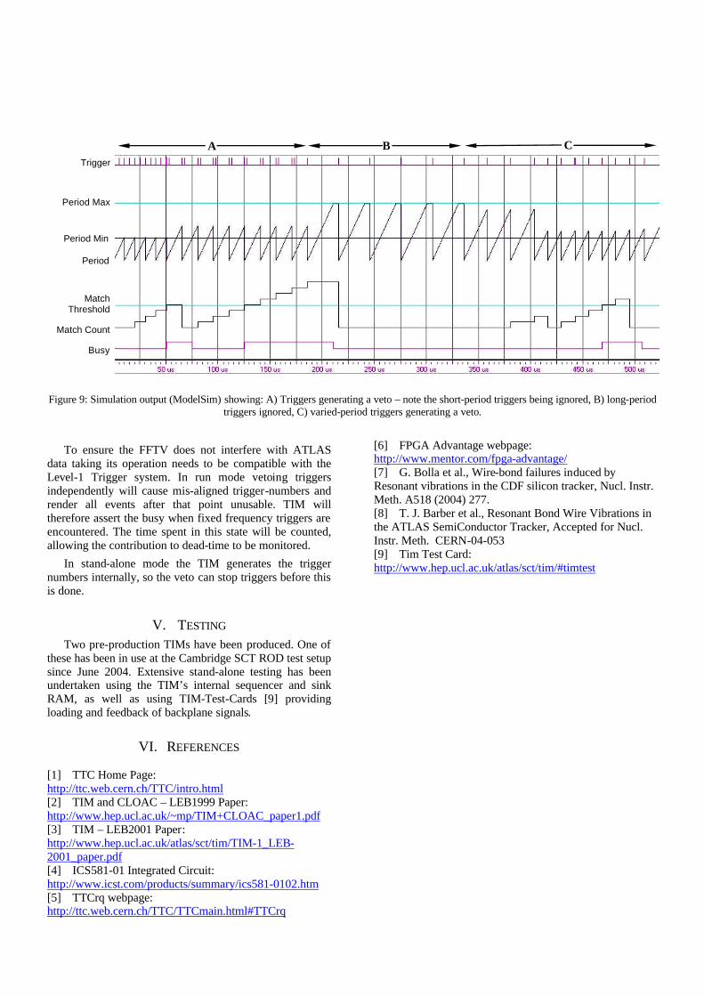
Figure 9: Simulation output (ModelSim) showing: A) Triggers generating a veto – note the short-period triggers being ignored, B) long-period triggers ignored, C) varied-period triggers generating a veto.
To ensure the FFTV does not interfere with ATLAS data taking its operation needs to be compatible with the Level-1 Trigger system. In run mode vetoing triggers independently will cause mis-aligned trigger-numbers and render all events after that point unusable. TIM will therefore assert the busy when fixed frequency triggers are encountered. The time spent in this state will be counted, allowing the contribution to dead-time to be monitored.
In stand-alone mode the TIM generates the trigger numbers internally, so the veto can stop triggers before this is done.
V. TESTING Two pre-production TIMs have been produced. One of
these has been in use at the Cambridge SCT ROD test setup since June 2004. Extensive stand-alone testing has been undertaken using the TIM’s internal sequencer and sink RAM, as well as using TIM-Test-Cards [9] providing loading and feedback of backplane signals.
VI. REFERENCES [1] TTC Home Page: http://ttc.web.cern.ch/TTC/intro.html [2] TIM and CLOAC – LEB1999 Paper: http://www.hep.ucl.ac.uk/~mp/TIM+CLOAC_paper1.pdf [3] TIM – LEB2001 Paper: http://www.hep.ucl.ac.uk/atlas/sct/tim/TIM-1_LEB-2001_paper.pdf [4] ICS581-01 Integrated Circuit: http://www.icst.com/products/summary/ics581-0102.htm [5] TTCrq webpage: http://ttc.web.cern.ch/TTC/TTCmain.html#TTCrq
[6] FPGA Advantage webpage: http://www.mentor.com/fpga-advantage/ [7] G. Bolla et al., Wire-bond failures induced by Resonant vibrations in the CDF silicon tracker, Nucl. Instr. Meth. A518 (2004) 277. [8] T. J. Barber et al., Resonant Bond Wire Vibrations in the ATLAS SemiConductor Tracker, Accepted for Nucl. Instr. Meth. CERN-04-053 [9] Tim Test Card: http://www.hep.ucl.ac.uk/atlas/sct/tim/#timtest
Trigger
Period Max
Period Min
Period
Match Threshold
Match Count
Busy
A B C