TMS320C672x DSP External Memory Interface (EMIF · TMS320C672x DSP External Memory Interface (EMIF)...
75
TMS320C672x DSP External Memory Interface (EMIF) User's Guide Literature Number: SPRU711C February 2005 – Revised April 2007
Transcript of TMS320C672x DSP External Memory Interface (EMIF · TMS320C672x DSP External Memory Interface (EMIF)...

TMS320C672x DSP External MemoryInterface (EMIF)
User's Guide
Literature Number: SPRU711C
February 2005–Revised April 2007

2 SPRU711C–February 2005–Revised April 2007Submit Documentation Feedback

Contents
Preface ............................................................................................................................... 7
1 Introduction/Feature Overview ..................................................................................... 91.1 Purpose of the Peripheral ........................................................................................ 10
1.2 Features ............................................................................................................ 10
1.2.1 32-bit EMIF................................................................................................ 10
1.2.2 16-bit EMIF................................................................................................ 10
1.3 Functional Block Diagram ........................................................................................ 11
2 Major Features/Common Architecture ......................................................................... 132.1 Clock Control....................................................................................................... 14
2.2 EMIF Requests .................................................................................................... 14
2.3 Pin Descriptions ................................................................................................... 15
2.4 SDRAM Controller and Interface ................................................................................ 16
2.4.1 SDRAM Commands ..................................................................................... 16
2.4.2 Interfacing to SDRAM.................................................................................... 17
2.4.3 SDRAM Configuration Registers ....................................................................... 20
2.4.4 SDRAM Auto-Initialization Sequence.................................................................. 21
2.4.5 SDRAM Configuration Procedure ...................................................................... 22
2.4.6 EMIF Refresh Controller................................................................................. 23
2.4.7 Self-Refresh Mode ....................................................................................... 24
2.4.8 SDRAM Read Operation ................................................................................ 24
2.4.9 SDRAM Write Operations ............................................................................... 25
2.4.10 Mapping from Logical Address to EMIF Pins........................................................ 27
2.5 Asynchronous Controller and Interface......................................................................... 28
2.5.1 Interfacing to Asynchronous Memory.................................................................. 29
2.5.2 Accessing Larger Asynchronous Memories .......................................................... 32
2.5.3 Configuring the EMIF for Asynchronous Accesses .................................................. 32
2.5.4 Read and Write Operations in WE Strobe Mode..................................................... 34
2.5.5 Read and Write Operation in Select Strobe Mode................................................... 38
2.5.6 NAND Flash Mode ....................................................................................... 41
2.5.7 Extended Wait Mode and the EM_WAIT Pin ......................................................... 44
2.6 Data Bus Parking.................................................................................................. 45
2.7 Reset and Initialization Considerations......................................................................... 45
2.8 Interrupt Support .................................................................................................. 45
2.8.1 Interrupt Events........................................................................................... 45
2.8.2 Interrupt Multiplexing..................................................................................... 46
2.9 Interrupt Processing............................................................................................... 46
2.10 Pin Multiplexing.................................................................................................... 46
2.11 Priority and Arbitration ............................................................................................ 47
2.12 System Considerations ........................................................................................... 47
2.12.1 Asynchronous Request Times......................................................................... 47
2.12.2 Cache Fill Requests .................................................................................... 48
2.13 Power Management............................................................................................... 48
2.14 Emulation Considerations ........................................................................................ 48
SPRU711C–February 2005–Revised April 2007 Contents 3Submit Documentation Feedback

3 Registers ................................................................................................................. 493.1 Introduction......................................................................................................... 50
3.2 Asynchronous Wait Cycle Configuration Register (AWCCR) ............................................... 51
3.3 SDRAM Configuration Register (SDCR) ....................................................................... 52
3.4 SDRAM Refresh Control Register (SDRCR) .................................................................. 54
3.5 Asynchronous Configuration Register (A1CR) ................................................................ 55
3.6 SDRAM Timing Register (SDTIMR) ............................................................................ 55
3.7 SDRAM Self Refresh Exit Timing Register (SDSRETR)..................................................... 57
3.8 EMIF Interrupt Raw Register (EIRR) ........................................................................... 58
3.9 EMIF Interrupt Masked Register (EIMR) ....................................................................... 59
3.10 EMIF Interrupt Mask Set Register (EIMSR) ................................................................... 60
3.11 EMIF Interrupt Mask Clear Register (EIMCR)................................................................. 61
3.12 NAND Flash Control Register (NANDFCR).................................................................... 62
3.13 NAND Flash Status Register (NANDFSR)..................................................................... 63
3.14 NAND Flash 1 ECC Register (NANDF1ECC) ................................................................. 63
4 Example Configuration .............................................................................................. 654.1 Hardware Interface................................................................................................ 66
4.2 SW Configuration.................................................................................................. 67
4.2.1 Configuring the SDRAM Interface...................................................................... 67
4.2.2 Configuring the Flash Interface......................................................................... 70
A Appendix A: Revision History .................................................................................... 73
4 Contents SPRU711C–February 2005–Revised April 2007Submit Documentation Feedback

List of Figures
1-1 EMIF Functional Block Diagram.......................................................................................... 112-1 Timing Waveform of SDRAM PRE Command ......................................................................... 172-2 EMIF to 2M x 16 x 4 bank SDRAM Interface........................................................................... 182-3 EMIF to 512K x 16 x 2 bank SDRAM Interface ........................................................................ 182-4 EMIF to 2M x 32 x 4 bank SDRAM Interface........................................................................... 182-5 EMIF to dual 4M x 16 x 4 bank SDRAM Interface ..................................................................... 192-6 Timing Waveform for Basic SDRAM Read Operation................................................................. 252-7 Timing Waveform for Basic SDRAM Write Operation ................................................................. 262-8 EMIF Asychronous Interface.............................................................................................. 292-9 EMIF to 8-bit Memory Interface .......................................................................................... 302-10 Common Asynchronous Interfaces ...................................................................................... 312-11 Timing Waveform of an Asynchronous Read Cycle in WE Strobe Mode........................................... 352-12 Timing Waveform of an Asynchronous Write Cycle in WE Strobe Mode........................................... 372-13 Timing Waveform of an Asynchronous Read Cycle in Select Strobe Mode ....................................... 392-14 Timing Waveform of an Asynchronous Write Cycle in Select Strobe Mode........................................ 402-15 EMIF to NAND Flash Interface ........................................................................................... 422-16 ECC Value for 8-Bit NAND Flash ........................................................................................ 433-1 Asynchronous Wait Cycle Configuration Register (AWCCR) [Offset 04h].......................................... 513-2 SDRAM Configuration Register (SDCR) [Offset 08h] ................................................................. 523-3 SDRAM Refresh Control Register (SDRCR) [Offset 0Ch] ............................................................ 543-4 Asynchronous 1 Configuration Register (A1CR) [Offset 10h] ........................................................ 553-5 SDRAM Timing Register (SDTIMR) [Offset 20h]....................................................................... 563-6 SDRAM Self Refresh Exit Timing Register (SDSRETR) [Offset 3Ch] .............................................. 573-7 EMIF Interrupt Raw Register (EIRR) [Offset 40h]...................................................................... 583-8 EMIF Interrupt Mask Register (EIMR) [Offset 44h] .................................................................... 593-9 EMIF Interrupt Mask Set Register (EIMSR) [Offset 48h].............................................................. 603-10 EMIF Interrupt Mask Clear Register (EIMCR) [Offset 4Ch]........................................................... 613-11 NAND Flash Control Register (NANDFCR)............................................................................. 623-12 NAND Flash Status Register (NANDFSR).............................................................................. 633-13 NAND Flash 1 ECC Register (NANDF1ECC) .......................................................................... 634-1 Example Configuration Interface ......................................................................................... 664-2 SDRAM Timing Register (SDTIMR) ..................................................................................... 684-3 SDRAM Self Refresh Exit Timing Register (SDSRETR).............................................................. 684-4 SDRAM Refresh Control Register (SDRCR) ........................................................................... 694-5 SDRAM Configuration Register (SDCR) ................................................................................ 694-6 LH28F800BJE-PTTL90 to EMIF Read Timing Waveforms........................................................... 704-7 LH28F800BJE-PTTL90 to EMIF Write Timing Waveforms ........................................................... 714-8 Asynchronous 1 Configuration Register (A1CR) [Offset 10h] ........................................................ 72
SPRU711C–February 2005–Revised April 2007 List of Figures 5Submit Documentation Feedback

List of Tables
2-1 EMIF Pins used to Access Both SDRAM and Asynchronous Memories ........................................... 152-2 EMIF Pins Specific to SDRAM ........................................................................................... 152-3 EMIF Pins Specific to Asynchronous Memory ......................................................................... 162-4 EMIF SDRAM Commands ................................................................................................ 162-5 Truth Table for SDRAM Commands..................................................................................... 172-6 32-bit EMIF Address Pin Connections................................................................................... 192-7 16-bit EMIF Address Pin Connections................................................................................... 202-8 Description of the SDRAM Configuration Register (SDCR) .......................................................... 202-9 Description of the SDRAM Refresh Control Register (SDRCR) ..................................................... 202-10 Description of the SDRAM Timing Register (SDTIMR) ............................................................... 212-11 Description of the SDRAM Self Refresh Exit Timing Register (SDSRETR) ........................................ 212-12 SDRAM LOAD MODE REGISTER Command ......................................................................... 222-13 Refresh Urgency Levels ................................................................................................... 232-14 Mapping from Logical Address to EMIF Pins for 32-bit SDRAM..................................................... 272-15 Mapping from Logical Address to EMIF Pins for 16-bit SDRAM..................................................... 282-16 WE Strobe Mode vs. Select Strobe Mode .............................................................................. 282-17 Description of the Asynchronous 1 Configuration Register (A1CR) ................................................. 322-18 Description of the Asynchronous Wait Cycle Configuration Register (AWCCR) .................................. 332-19 Description of the EMIF Interrupt Mask Set Register (EIMSR) ...................................................... 342-20 Description of the EMIF Interrupt Mast Clear Register (EIMCR) .................................................... 342-21 Asynchronous Read Operation in WE Strobe Mode .................................................................. 342-22 Asynchronous Write Operation in WE Strobe Mode................................................................... 362-23 Asynchronous Read Operation in Select Strobe Mode ............................................................... 382-24 Asynchronous Write Operation in Select Strobe Mode ............................................................... 392-25 Description of the NAND Flash Control Register (NANDFCR)....................................................... 412-26 Interrupt Monitor and Control Bit Fields ................................................................................. 463-1 External Memory Interface (EMIF) Registers........................................................................... 503-2 Asynchronous Wait Cycle Configuration Register (AWCCR) Field Descriptions .................................. 513-3 SDRAM Configuration Register (SDCR) Field Descriptions.......................................................... 523-4 SDRAM Refresh Control Register (SDRCR) Field Descriptions ..................................................... 543-5 Asynchronous 1 Configuration Register (A1CR) Field Descriptions................................................. 553-6 SDRAM Timing Register (SDTIMR) Field Descriptions ............................................................... 563-7 SDRAM Self Refresh Exit Timing Register (SDSRETR) Field Descriptions ....................................... 573-8 EMIF Interrupt Raw Register (EIRR) Field Descriptions .............................................................. 583-9 EMIF Interrupt Mask Register (EIMR) Field Descriptions............................................................. 593-10 EMIF Interrupt Mask Set Register (EIMSR) Field Descriptions ...................................................... 603-11 EMIF Interrupt Mask Clear Register (EIMCR) Field Descriptions ................................................... 613-12 NAND Flash Control Register (NANDFCR) Field Descriptions ...................................................... 623-13 NAND Flash Status Register (NANDFSR) Field Descriptions ....................................................... 633-14 NAND Flash 1 ECC Register (NANDF1ECC) Field Descriptions.................................................... 634-1 SR Field Value For the EMIF to K4S641632H-TC(L)70 Interface ................................................... 674-2 SDTIMR Field Calculations for the EMIF to K4S641632H-TC(L)70 Interface ..................................... 674-3 RR Calculation for the EMIF to K4S641632H-TC(L)70 Interface .................................................... 684-4 RR Calculation for the EMIF to K4S641632H-TC(L)70 Interface .................................................... 684-5 SDCR Field Values For the EMIF to K4S641632H-TC(L)70 Interface.............................................. 694-6 AC Characteristics for a Read Access .................................................................................. 704-7 AC Characteristics for a Write Access .................................................................................. 70A-1 Changes in This Revision ................................................................................................. 73
6 List of Tables SPRU711C–February 2005–Revised April 2007Submit Documentation Feedback

PrefaceSPRU711C–February 2005–Revised April 2007
Read This First
Trademarks
TMS320C672x, TMS320C6000, C6000, TMS320C62x, TMS320C67x, Code Composer Studio aretrademarks of Texas Instruments.
About this Manual
This document describes the operation of the external memory interface (EMIF) in the TMS320C672x™digital signal processors (DSPs) of the TMS320C6000™ family. This document contains the followingchapters:• Chapter 1 provides information about the features, purpose and use of the EMIF.• Chapter 2 provides details about the architecture and operaton of the EMIF.• Chapter 3 provides a list of registers and register descriptions that are used in the EMIF.• Chapter 4 presents an example of interfacing the EMIF to both an SDR SDRAM device and an
asychronous flash device.
Notational Conventions
This document uses the following conventions:• Hexadecimal numbers are shown with the suffix h. For example, the following number is 40
hexadecimal (decimal 64): 40h.• Registers in this document are shown in figures and described in tables
– Each register figure shows a rectangle divided into fields that represent the fields of the register.Each field is labeled with its bit name, its beginning and ending bit numbers above, and itsread/write properties below. A legend explains the notation used for the properties.
– Reserved bits in a register figure designate a bit that is used for future device expansion.
Related Documentation From Texas Instruments
The following documents describe the C6000™ devices and related support tools. Copies of thesedocuments are available on the Internet at www.ti.com. Tip: Enter the literature number in the search boxprovided at www.ti.com.
TMS320C672x DSP Peripherals Overview Reference Guide (literature number SPRU723) describesperipherals available on the TMS320C672x™ DSPs.
TMS320C6000 Technical Brief (literature number SPRU197) gives an introduction to the TMS320C62x™and TMS320C67x™ DSPs, development tools, and third-party support.
TMS320c672xDSP CPU and Instruction Set Reference Guide (literature number SPRU733) describes theTMS320C672x™ CPU architecture, instruction set, pipeline, and interrupts for these digital signalprocessors.
TMS320C6000 Code Composer Studio Tutorial (literature number SPRU301) introduces the CodeComposer Studio™ integrated development environment and software tools.
TMS320C6000 Programmer's Guide (literature number SPRU198) describes ways to optimize C andassembly code for the TMS320C6000 DSPs and includes application program examples.
Code Composer Studio Application Programming Interface Reference Guide (literature number SPRU321)describes the Code Composer Studio™ application programming interface (API), which allows you toprogram custom plug-ins for Code Composer.
SPRU711C–February 2005–Revised April 2007 Read This First 7Submit Documentation Feedback

www.ti.com
Read This First8 SPRU711C–February 2005–Revised April 2007Submit Documentation Feedback

Chapter 1SPRU711C–February 2005–Revised April 2007
Introduction/Feature Overview
This chapter provides information about the features, purpose, and use of the externalmemory interface (EMIF). It also provides a block diagram of the EMIF that shows itsinternal connections and external pins.
Topic .................................................................................................. Page
1.1 Purpose of the Peripheral .......................................................... 101.2 Features................................................................................... 101.3 Functional Block Diagram .......................................................... 11
SPRU711C–February 2005–Revised April 2007 Introduction/Feature Overview 9Submit Documentation Feedback

www.ti.com
1.1 Purpose of the Peripheral
1.2 Features
1.2.1 32-bit EMIF
1.2.2 16-bit EMIF
Purpose of the Peripheral
The purpose of this EMIF is to provide a means for the the digital signal processor (DSP) to connect to avariety of external devices including:
• Single data rate (SDR) SDRAM• Asynchronous devices including NOR Flash, NAND Flash, and SRAM• Host processor interfaces such as the host port interface (HPI) on a Texas Instruments DSP
The most common use for the EMIF is to interface with both a flash device and an SDRAM devicesimultaneously. Chapter 4 contains an example of operating the EMIF in this configuration.
The EMIF includes many features to enhance the ease and flexibility of connecting to external SDRSDRAM and asynchronous devices. Two versions of the EMIF exist, with the primay difference betweenthe two versions being the width of the data bus. Depending on the device, the EMIF data bus is either 32bits or 16 bits. Other differences between the two versions of the EMIF exist and are enumerated in thefollowing subsections. Please refer to the data manual for a specific device to determine which version ofthe EMIF is included.
SDR SDRAM features include support for:
• Up to 512 Mb JESD21-C standard-compliant SDR SDRAM devices• 16- and 32-bit data bus widths• 1, 2, or 4 internal SDRAM banks• SDRAM burst accesses of length 4 or 8, depending on the data bus width chosen• Programmable SDRAM timing parameters, CAS latency, and refresh rate• Prioritized refresh scheme to decrease access latency• Self-refresh mode to reduce power consumption• Sequential burst type. Interleave burst type not supported.
Asynchronous features include support for:• An addressable space of up to 128KB, expandable using GPIO pins• 8-, 16-, and 32-bit data bus widths• Programmable cycle timings such as setup, strobe, and hold times and turnaround time• Programmable extended wait access cycles for slower devices• Write-enable strobe mode for interfacing with multiple 8-bit devices• Connecting as a host to a TI DSP HPI interface
SDR SDRAM features include support for:
• Up to 128 Mb JESD21-C standard compliant SDR SDRAM devices• 16-bit data bus widths• 1, 2, and 4 internal SDRAM banks• SDRAM burst accesses of length 8• Programmable SDRAM timing parameters, CAS latency, and refresh rate• Prioritized refresh scheme to decrease access latency• Self-refresh mode to reduce power consumption• Sequential burst type. Interleave burst type not supported.
10 Introduction/Feature Overview SPRU711C–February 2005–Revised April 2007Submit Documentation Feedback

www.ti.com
1.3 Functional Block Diagram
EM_CS[0]EM_CASEM_RASEM_CLKEM_CKE
EM_CS[2]EM_OEEM_RW
EM_WAIT
EM_WEEM_BA[1:0]
EM_WE_DQM[x:0]EM_D[x:0]EM_A[x:0]
EMIF
dMAX MAX0
dMAX MAX1
UHPI
CPU DMP
CPU PMP
SDRAMinterface
Asynchronousinterface
Shared SDRAMand asynchronousinterface
Functional Block Diagram
Asynchronous features include support for:• An addressable space of up to 32KB, expandable using GPIO pins• 8- and 16-bit data bus widths• Programmable cycle timings such as setup, strobe, and hold times as well as turnaround time• Write-enable strobe mode for interfacing with multiple 8-bit devices• Connecting as a host to a TI DSP HPI interface
Figure 1-1 illustrates the connections between the EMIF and its internal requesters, along with theexternal EMIF pins. Section 2.2 contains a description of the entities internal to the DSP that can can sendrequests to the EMIF, along with their prioritization. Section 2.3 describes the EMIF's external pins andsummarizes their purpose when interfacing with SDRAM and asynchronous devices.
Figure 1-1. EMIF Functional Block Diagram
SPRU711C–February 2005–Revised April 2007 Introduction/Feature Overview 11Submit Documentation Feedback

www.ti.com
Introduction/Feature Overview12 SPRU711C–February 2005–Revised April 2007Submit Documentation Feedback

Chapter 2SPRU711C–February 2005–Revised April 2007
Major Features/Common Architecture
This section provides details about the architecture and operation of the EMIF. Both theSDRAM and asynchronous interface are covered, along with other system-relatedissues such as clock control and pin multiplexing.
Topic .................................................................................................. Page
2.1 Clock Control ........................................................................... 142.2 EMIF Requests.......................................................................... 142.3 Pin Descriptions ....................................................................... 152.4 SDRAM Controller and Interface ................................................. 162.5 Asynchronous Controller and Interface ....................................... 282.6 Data Bus Parking ...................................................................... 452.7 Reset and Initialization Considerations........................................ 452.8 Interrupt Support ...................................................................... 452.9 Interrupt Processing.................................................................. 462.10 Pin Multiplexing ........................................................................ 462.11 Priority and Arbitration .............................................................. 472.12 System Considerations.............................................................. 472.13 Power Management ................................................................... 482.14 Emulation Considerations .......................................................... 48
SPRU711C–February 2005–Revised April 2007 Major Features/Common Architecture 13Submit Documentation Feedback

www.ti.com
2.1 Clock Control
2.2 EMIF Requests
Clock Control
The EMIF's internal clock is sourced from the SYSCLK3 clock domain of the DSP's PLL controller andcannot be sourced directly from an external input clock. The frequency of the SYSCLK3 clock domain iscontrolled by configuring the PLL controller's multipliers and dividers. Refer to the device Data Manual formore information on selecting the frequency of SYSCLK3.
The EMIF's clock is output on the EM_CLK pin and should be used when interfacing to externalmemories. The EMIF clock (EM_CLK) does not run during device reset. When the RESET pin is releasedand after the PLL controller releases the device from reset, EM_CLK begins to oscillate at a frequencydetermined by the PLL controller.
Five different sources within the C67x DSP can make requests to the EMIF. These requests consist ofaccesses to SDRAM memory, asynchronous memory, and EMIF registers. Because the EMIF canprocess only one request at a time, a high performance crossbar switch exists within the DSP to provideprioritized requests from the different sources to the EMIF. The sources are listed below from highest tolowest priority:
1. dMAX MAX0 (DMA)2. dMAX MAX1 (DMA)3. UHPI (Host Port Interface)4. DMP (CPU Data Master Port)5. PMP (CPU Program Master Port)
If a request is submitted from two or more sources simultaneously, the crossbar switch will forward thehighest priority request to the EMIF first. Upon completion of a request, the crossbar switch againevaluates the pending requests and forwards the highest priority pending request to the EMIF.
When the EMIF receives a request, it may or may not be immediately processed. In some cases, theEMIF will perform one or more auto refresh cycles before processing the request. For details on theEMIF's internal arbitration between performing requests and performing auto refresh cycles, seeSection 2.11.
Major Features/Common Architecture14 SPRU711C–February 2005–Revised April 2007Submit Documentation Feedback

www.ti.com
2.3 Pin Descriptions
Pin Descriptions
This section describes the function of each of the EMIF pins.
Table 2-1. EMIF Pins used to Access Both SDRAM and Asynchronous Memories
Pins(s) I/O Description
EM_D[x:0] I/O EMIF data bus.The number of available data bus pins varies among devices. See the device Data Manual fordetails.
EM_ A[x:0] O EMIF address bus.When interfacing to an SDRAM device, these pins are primarily used to provide the row andcolumn address to the SDRAM. The mapping from the internal program address to the externalvalues placed on these pins can be found in Table 2-14 and Table 2-15. EM_A[10] is also usedduring the PRE command to select which banks to deactivate.When interfacing to an asynchronous device, these pins are used in conjunction with the EM_BApins to form the address that is sent to the device. The mapping from the internal programaddress to the external values placed on these pins can be found in Section 2.5.1.The number of available address pins varies among devices. See the device Data Manual forspecific details.
EM_BA[1:0] O EMIF bank address.When interfacing to an SDRAM device, these pins are used to provide the bank address inputs toto the SDRAM. The mapping from the internal program address to the external values placed onthese pins can be found in Table 2-14 and Table 2-15.When interfacing to an asynchronous device, these pins are used in conjunction with the EM_Apins to form the address that is sent to the device. The mapping from the internal programaddress to the external values placed on these pins can be found in Section 2.5.1.
EM_WE_DQM[x:0] O Active-low write strobes or byte enables.When interfacing to SDRAM, these pins are connected to the DQM pins of the SDRAM toindividually enable/disable each of the bytes in a data access.When interfacing to an asynchronous device, these pins can either serve as byte enables (DQM)or byte write strobes (WE). See Section 2.5 for details.
EM_WE O Active-low write enable.When interfacing to SDRAM, this pin is connected to the WE pin of the SDRAM and is used tosend commands to the device.When interfacing to an asynchronous device, this pin provides a signal which is active-low duringthe strobe period of an asynchronous write access cycle.
Table 2-2. EMIF Pins Specific to SDRAM
Pin(s) I/O Description
EM_CS[0] O Active-low chip enable pin for SDRAM devices.This pin is connected to the chip-select pin of the attached SDRAM device and is used forenabling/disabling commands. By default, the EMIF keeps this SDRAM chip select active, even if theEMIF is not interfaced with an SDRAM device. This pin is deactivated when accessing theasynchronous memory bank and is reactivated on completion of the asynchronous assess.
EM_RAS O Active-low row address strobe pin.This pin is connected to the RAS pin of the attached SDRAM device and is used for sendingcommands to the device.
EM_CAS O Active-low column address strobe pin.This pin is connected to the CAS pin of the attached SDRAM device and is used for sendingcommands to the device.
EM_CKE O Clock enable pin.This pin is connected to the CKE pin of the attached SDRAM device and is used for issuing the SELFREFRESH command which places the device in self refresh mode. See Section 2.4.7 for details.
EM_CLK O SDRAM clock pin.This pin is connected to the CLK pin of the attached SDRAM device. See Section 2.1 for details onthe clock signal.
SPRU711C–February 2005–Revised April 2007 Major Features/Common Architecture 15Submit Documentation Feedback
www.ti.com
2.4 SDRAM Controller and Interface
2.4.1 SDRAM Commands
SDRAM Controller and Interface
Table 2-3. EMIF Pins Specific to Asynchronous Memory
Pin(s) I/O Description
EM_CS[2] O Active-low chip enable pin for asynchronous devices.This pin is meant to be connected to the chip-select pin of the attached asynchronous device. Thispin is active only during accesses to the asynchronous memory.
EM_WAIT I Wait input with programmable polarity / NAND Flash ready inputA connected asynchronous device can extend the strobe period of an access cycle by asserting theEM_WAIT input to the EMIF as described in Section 2.5.7. To enable this functionality, the EW bit inthe Asynchronous 1 Configuration Register (A1CR) must be set to 1. In addition, the WP0 bit inA1CR must be configured to define the polarity of the EM_WAIT pin. The EM_WAIT pin is notavailable on all devices. See the device Data Manual for details.When the CS2NAND bit in the NAND Flash Control Register (NANDFCR) is set, this pin insteadfunctions as a NAND Flash ready input.
EM_OE O Active-low pin enable for asynchronous devices.This pin provides a signal which is active-low during the strobe period of an asynchronous readaccess cycle.
EM_RW O Read/Write select pin.This pin is high for the duration of an asynchronous read access cycle and low for the duration of anasynchronous write access cycle.
The EMIF can gluelessly interface to most standard SDR SDRAM devices and supports such features asself refresh mode and prioritized refresh. In addition, it provides flexibility through programmableparameters such as the refresh rate, CAS latency, and many SDRAM timing parameters. The followingsections include details on how to interface and properly configure the EMIF to perform read and writeoperations to externally connected SDR SDRAM devices. Also, Chapter 4 provides a detailed example ofinterfacing the EMIF to a common SDRAM device.
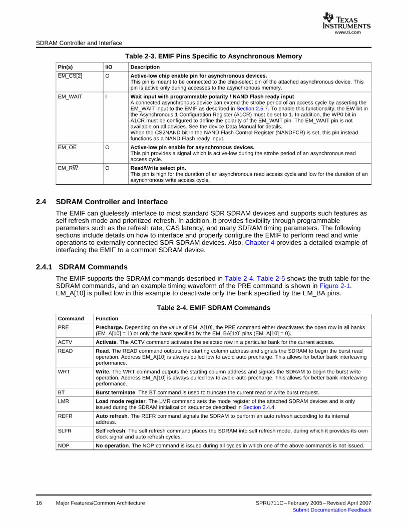
The EMIF supports the SDRAM commands described in Table 2-4. Table 2-5 shows the truth table for theSDRAM commands, and an example timing waveform of the PRE command is shown in Figure 2-1.EM_A[10] is pulled low in this example to deactivate only the bank specified by the EM_BA pins.
Table 2-4. EMIF SDRAM Commands
Command Function
PRE Precharge. Depending on the value of EM_A[10], the PRE command either deactivates the open row in all banks(EM_A[10] = 1) or only the bank specified by the EM_BA[1:0] pins (EM_A[10] = 0).
ACTV Activate. The ACTV command activates the selected row in a particular bank for the current access.
READ Read. The READ command outputs the starting column address and signals the SDRAM to begin the burst readoperation. Address EM_A[10] is always pulled low to avoid auto precharge. This allows for better bank interleavingperformance.
WRT Write. The WRT command outputs the starting column address and signals the SDRAM to begin the burst writeoperation. Address EM_A[10] is always pulled low to avoid auto precharge. This allows for better bank interleavingperformance.
BT Burst terminate. The BT command is used to truncate the current read or write burst request.
LMR Load mode register. The LMR command sets the mode register of the attached SDRAM devices and is onlyissued during the SDRAM initialization sequence described in Section 2.4.4.
REFR Auto refresh. The REFR command signals the SDRAM to perform an auto refresh according to its internaladdress.
SLFR Self refresh. The self refresh command places the SDRAM into self refresh mode, during which it provides its ownclock signal and auto refresh cycles.
NOP No operation. The NOP command is issued during all cycles in which one of the above commands is not issued.
Major Features/Common Architecture16 SPRU711C–February 2005–Revised April 2007Submit Documentation Feedback

www.ti.com
PRE
EM_CLK
EM_CS[0]
EM_WE_DQM
EM_BA
EM_A
EM_RAS
EM_CAS
EM_WE
Bank
EM_A[10]=0
2.4.2 Interfacing to SDRAM
SDRAM Controller and Interface
Table 2-5. Truth Table for SDRAM CommandsSDRAM Pins: CKE CS RAS CAS WE BA[1:0] A[12:11] A[10] A[9:0]
EMIF Pins: EM_CKE EM_CS[0] EM_RAS EM_CAS EM_WE EM_BA[1:0] EM_A[12:11] (1) EM_A[10] EM_A[9:0]
PRE H L L H L Bank/X X L/H X
ACTV H L L H H Bank Row Row Row
READ H L H L H Bank Column L Column
WRT H L H L L Bank Column L Column
BT H L H H L X X X X
LMR H L L L L X Mode Mode Mode
REFR H L L L H X X X X
SLFR L L L L H X X X X
NOP H L H H H X X X X
(1) EM_A[12] is not available on all devices. See the device Data Manual for details.
Figure 2-1. Timing Waveform of SDRAM PRE Command
The EMIF supports a glueless interface to SDRAM devices with the following characteristics:• Pre-charge bit is A[10]• The number of column address bits is 8, 9, or 10• The number of row address bits allowed varies depending on the DSP device:
– for DSP devices with 12 EMIF address pins: 11- or 12-row address bits– for DSP devices with 13 EMIF address pins: 11-, 12-, or 13-row address bits
• The number of internal banks is 1, 2, or 4
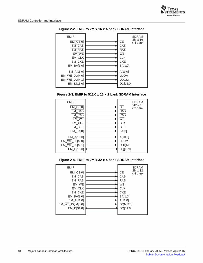
Figure 2-2 shows an interface between the EMIF and a 2M x 16 x 4 bank SDRAM device, and Figure 2-3shows an interface between the EMIF and a 512K x 16 x 2 bank SDRAM device. In addition, Figure 2-4shows an interface between the EMIF and a 2M x 32 x 4 bank SDRAM device and Figure 2-5 shows aninterface between the EMIF and two 4M x 16 x 4 bank SDRAM devices. Refer to Table 2-6 for anadditional list of commonly-supported SDRAM devices and the required connections for the address pins.
SPRU711C–February 2005–Revised April 2007 Major Features/Common Architecture 17Submit Documentation Feedback
www.ti.com
EM_CS[0]EM_CASEM_RASEM_WE
EM_CLKEM_CKE
EM_BA[1:0]
EM_A[11:0]EM_WE_DQM[0]EM_WE_DQM[1]
EM_D[15:0]
EMIF
CECASRASWECLKCKEBA[1:0]
A[11:0]LDQMUDQMDQ[15:0]
SDRAM2M x 16x 4 bank
EM_CS[0]EM_CASEM_RASEM_WE
EM_CLKEM_CKE
EM_BA[0]
EM_A[10:0]EM_WE_DQM[0]EM_WE_DQM[1]
EM_D[15:0]
EMIF
CECASRASWECLKCKEBA[0]
A[10:0]LDQMUDQMDQ[15:0]
SDRAM512 x 16x 2 bank
EM_CS[0]EM_CASEM_RASEM_WE
EM_CLKEM_CKE
EM_BA[1:0]EM_A[11:0]
EM_WE_DQM[3:0]EM_D[31:0]
EMIF
CECASRASWECLKCKEBA[1:0]A[11:0]DQM[3:0]DQ[31:0]
SDRAM2M x 32x 4 bank
SDRAM Controller and Interface
Figure 2-2. EMIF to 2M x 16 x 4 bank SDRAM Interface
Figure 2-3. EMIF to 512K x 16 x 2 bank SDRAM Interface
Figure 2-4. EMIF to 2M x 32 x 4 bank SDRAM Interface
18 Major Features/Common Architecture SPRU711C–February 2005–Revised April 2007Submit Documentation Feedback

www.ti.com
EM_CS[0]EM_CASEM_RASEM_WE
EM_CLKEM_CKE
EM_BA[1:0]
EM_A[12:0]EM_WE_DQM[0]EM_WE_DQM[1]
EM_D[15:0]
EMIF
CECASRASWECLKCKEBA[1:0]
A[12:0]LDQMUDQMDQ[15:0]
SDRAM4M x 16x 4 bank
EM_WE_DQM[2]EM_WE_DQM[3]
EM_D[31:16]
LDQMUDQMDQ[15:0]
BA[1:0]CKECLKWERASCAS
A[12:0]
CE x 4 bank
SDRAM4M x 16
SDRAM Controller and Interface
Figure 2-5. EMIF to dual 4M x 16 x 4 bank SDRAM Interface
Table 2-6. 32-bit EMIF Address Pin Connections
SDRAM Size Width Banks Address Pins
SDRAM A[10:0]16M bits x16 2
EMIF EM_A[10:0]
SDRAM A[11:0]x16 4
EMIF EM_A[11:0]64M bits
SDRAM A[10:0]x32 4
EMIF EM_A[10:0]
SDRAM A[11:0]X16 4
EMIF EM_A[11:0]128M bits
SDRAM A[11:0]X32 4
EMIF EM_A[11:0]
SDRAM A[12:0]x16 4
EMIF EM_A[12:0]256M bits
SDRAM A[11:0]x32 4
EMIF EM_A[11:0]
SDRAM A[12:0]512M bits X16 4
EMIF EM_A[12:0]
SPRU711C–February 2005–Revised April 2007 Major Features/Common Architecture 19Submit Documentation Feedback

www.ti.com
2.4.3 SDRAM Configuration Registers
SDRAM Controller and Interface
Table 2-7. 16-bit EMIF Address Pin Connections
SDRAM Size Width Banks Address Pins
SDRAM A[10:0]16M bits x16 2
EMIF EM_A[10:0]
SDRAM A[11:0]64M bits x16 4
EMIF EM_A[11:0]
SDRAM A[11:0]128M bits X16 4
EMIF EM_A[11:0]
The operation of the EMIF's SDRAM interface is controlled by programming the appropriate configurationregisters. This section describes the purpose and function of each configuration register, but Chapter 3should be referenced for a more detailed description of each register, including the default registers valuesand bit-field positions. The tables below list the four SDRAM configuration registers, along with adescription of each of their programmable fields.
Table 2-8. Description of the SDRAM Configuration Register (SDCR)
Parameter Description
NM Narrow Mode. This bit defines the width of the data bus between the EMIF and the attachedSDRAM device. When set to 1, the data bus is set to 16-bits. When set to 0, the data bus is set to32-bits. Not all devices support a 32-bit data bus. Refer to the device Data Manual for details.
CL CAS latency. This field defines the number of clock cycles between when an SDRAM issues aREAD command and when the first piece of data appears on the bus. The value in this field issent to the attached SDRAM device via the LOAD MODE REGISTER command during theSDRAM initialization procedure as described in Section 2.4.4. Only values of 2h (CAS latency =2) and 3h (CAS latency = 3) are supported and should be written to this field. A 1 must besimultaneously written to the BIT11_9LOCK bit field of SDCR in order to write to the CL bit field.
IBANK Number of Internal SDRAM Banks. This field defines the number of banks inside the attachedSDRAM devices in the following way:
• When IBANK = 0, 1 internal bank is used• When IBANK = 1h, 2 internal banks are used• When IBANK = 2h, 4 internal banks are used
This field vallue affects the mapping of logical addresses to SDRAM row, column, and bankaddresses. See Section 2.4.10 for details.
PAGESIZE Page Size. This field defines the internal page size of the attached SDRAM devices in thefollowing way:
• When PAGESIZE = 0, 256-word pages are used• When PAGESIZE = 1h, 512-word pages are used• When PAGESIZE = 2h, 1024-word pages are used
This field value affects the mapping of logical addresses to SDRAM row, column, and bankaddresses. See Section 2.4.10 for details.
Note: Writing to any of the fields in SDCR will cause the EMIF to abandon whatever it is currently doingand trigger the SDRAM initialization procedure described in Section 2.4.4.
Table 2-9. Description of the SDRAM Refresh Control Register (SDRCR)
Parameter Description
RR Refresh Rate. This field controls the rate at which attached SDRAM devices will be refreshed.The equation below can be used to determine the required value of RR for an SDRAM device:
• RR <= fEM_CLK / (Required SDRAM Refresh Rate)More information about the operation of the SDRAM refresh controller can be found inSection 2.4.6.
Major Features/Common Architecture20 SPRU711C–February 2005–Revised April 2007Submit Documentation Feedback

www.ti.com
2.4.4 SDRAM Auto-Initialization Sequence
SDRAM Controller and Interface
Table 2-10. Description of the SDRAM Timing Register (SDTIMR)
Parameter Description
T_RFC SDRAM Timing Parameters. These fields configure the EMIF to comply with the AC timingT_RP requirements of the attached SDRAM devices. This allows the EMIF to avoid violating SDRAMT_RCD timing constraints and to more efficiently schedule its operations. More details about each ofT_WR these parameters can be found in the register description inSection 3.6. These parameters shouldT_RAS be set to satisfy the corresponding timing requirements found in the SDRAM's datasheet.T_RCT_RRD
Table 2-11. Description of the SDRAM Self Refresh Exit Timing Register (SDSRETR)
Parameter Description
T_XS Self Refresh Exit Parameter. The T_XS field of this register informs the EMIF about theminimum number of EM_CLK cycles required between exiting Self Refresh and issuing anycommand. This parameter should be set to satisfy the tXSR value for the attached SDRAM device.
The EMIF automatically performs an SDRAM initialization sequence, regardless of whether it is interfacedto an SDRAM device, when either of the following two events occur:• The EMIF comes out of reset. No memory accesses to the SDRAM and Asynchronous interfaces are
performed until this auto-initialization is complete.• A write is performed to any of the three least significant bytes of the SDRAM Configuration Register
(SDCR)
An SDRAM initialization sequence consists of the following steps:
1. If the initialization sequence is activated by a write to SDCR, and if any of the SDRAM banks are open,the EMIF issues a PRE command with EM_A[10] held high to indicate all banks. This is done so thatthe maximum ACTV to PRE timing for an SDRAM is not violated.
2. The EMIF drives EM_CKE high and begins continuously issuing NOP commands until eight SDRAMrefresh intervals have elapsed. An SDRAM refresh interval is equal to the value of the RR field ofSDRAM Refresh Control Register (SDRCR), divided by the frequency of EM_CLK (RR/fEM_CLK). Thisstep is used to avoid violating the Power-up constrait of most SDRAM devices that requires 100µs(sometimes 200µs) between receiving stable Vdd and CLK and the issuing of a PRE command.Depending on the frequency of EM_CLK, this step may or may not be sufficient to avoid violating theSDRAM constraint. See Section 2.4.5 for more information.
3. After the refresh intervals have elapsed, the EMIF issues a PRE command with EM_A[10] held high toindicate all banks.
4. The EMIF issues eight AUTO REFRESH commands.5. The EMIF issues the LMR command with the EM_A[11:0] pins set as described in Section 2.4.4.1.6. Finally, the EMIF performs a refresh cycle, which consists of the following steps:
a. Issuing a PRE command with EM_A[10] held high if any banks are openb. Issuing a REF command
SPRU711C–February 2005–Revised April 2007 Major Features/Common Architecture 21Submit Documentation Feedback

www.ti.com
2.4.4.1 LMR Command used in the SDRAM Auto-Initialization Sequence
2.4.5 SDRAM Configuration Procedure
SDRAM Controller and Interface
Table 2-12. SDRAM LOAD MODE REGISTER Command
EM_A[11:7] EM_A[6:4] EM_A[3] EM_A[2:0]
0 (Write bursts are These bits control the CAS latency of the 0 (Sequential These bits control the burst length of theof the programmed SDRAM and are set according to CL field in Burst Type. SDRAM and are set according to the NMburst length in the SDRAM Configuration Register (SDCR) Interleaved field in the SDRAM Configuration RegisterEM_A[2:0]) as follows: Burst Type not (SDCR) as follows:
supported)• If CL = 2, EM_A[6:4] = 2h • If NM = 0, EM_A[2:0] = 2h(CAS latency = 2) (Burst Length = 4)
• If CL = 3, EM_A[6:4] = 3h • If NM = 1, EM_A[2:0] = 3h(CAS latency = 3) (Burst Length = 8)
There are two different SDRAM configuration procedures. Although the EMIF automatically performs theSDRAM initialization sequence described in Section 2.4.4 when coming out of reset, it is recommended tofollow one of the procedure listed below before performing any EMIF memory requests. Procedure Ashould be followed if it is determined that the the SDRAM Power-up constraint was not violated during theSDRAM Auto-Initialization Sequency detailed in Section 2.4.4 on coming out of Reset. The SDRAMPower-up constraint specifies that 100µs (sometimes 200µs) should exits between receiving stable Vddand CLK and the issuing of a PRE command. Procedure B should be followed if the SDRAM Power-upconstraint was violated. The 100µs (200µs) SDRAM Power-up constraint will be violated if the frequencyof EM_CLK is greater than 32 MHz (16 MHz) during SDRAM Auto-Initialization Sequence. This is becausethe value of the RR field at Reset is 190h. Procedure B should be followed if there is any doubt that thePower-up constraint was met.
Following is the procedure to be followed if the SDRAM Power-up constraint was NOT violated(Procedure A):
1. Place the SDRAM into Self-Refresh Mode by setting the SR bit of SDCR to 1. A byte-write to the upperbyte of SDCR should be used to avoid restarting the SDRAM Auto-Initialization Sequence described inSection 2.4.4. The SDRAM should be placed into Self-Refresh mode when changing the frequency ofEM_CLK to avoid incurring the 100µs Power-up constraint again.
2. Program the DSP's PLL Controller to provide the desired EM_CLK clock frequency on the SYSCLK3clock domain. Refer to the device Data Manual for details on programming the PLL Controller. Thefrequency of the memory clock must meet the timing requirements in the SDRAM manufacturer'sdocumentation and the timing limitations shown in the electrical specifications of the device DataManual.
3. Remove the SDRAM from Self-Refresh Mode by clearing the SR bit of SDCR to 0. A byte-write to theupper byte of SDCR should be used to avoid restarting the SDRAM Auto-Initialization Sequencedescribed in Section 2.4.4.
4. Program SDTIMR and SDSRETR to satisfy the timing requirements for the attached SDRAM device.The timing parameters should be taken from the SDRAM datasheet.
5. Program the RR field of SDRCR to match that of the attached device's refresh interval. SeeSection 2.4.6.1 details on determining the appropriate value.
6. Program SDCR to match the characteristics of the attached SDRAM device. This will cause theauto-initialization sequence in Section 2.4.4 to be re-run. This second initialization generally takesmuch less time due to the increased frequency of EM_CLK.
Following is the procedure to be followed if the SDRAM Power-up constraint was violated (Procedure B):
1. Program the DSP's PLL Controller to provide the desired EM_CLK clock frequency on the SYSCLK3clock domain. Refer to the device Data Manual for details on programming the PLL Controller. Thefrequency of the memory clock must meet the timing requirements in the SDRAM manufacturer'sdocumentation and the timing limitations shown in the electrical specifications of the device DataManual.
22 Major Features/Common Architecture SPRU711C–February 2005–Revised April 2007Submit Documentation Feedback

www.ti.com
2.4.6 EMIF Refresh Controller
SDRAM Controller and Interface
2. Program SDTIMR and SDSRETR to satisfy the timing requirements for the attached SDRAM device.The timing parameters should be taken from the SDRAM datasheet.
3. Program the RR field of SDRCR such that the following equation is satisfied: (RR * 8) / (fEM_CLK) > 100µs (or 200µs). For example, an EM_CLK frequency of 100MHz would require setting RR to 1251(0x4E3) or higher to meet a 100µs constraint.
4. Program SDCR to match the characteristics of the attached SDRAM device. This will cause theauto-initialization sequence in Section 2.4.4 to be re-run with the new value of RR.
5. Perform a read from the SDRAM to guarantee that step 5 of this procedure will occur after theinitialization process has completed. Alternatively, wait for 200 µs instead of performing a read.
6. Finally, program the RR field to match that of the attached device's refresh interval. SeeSection 2.4.6.1 details on determining the appropriate value.
After following the above procedure, the EMIF is ready to perform accesses to the attached SDRAMdevice. See Chapter 4 for an example of configuring the SDRAM interface.
An SDRAM device requires that each of its rows be refreshed at a minimum required rate. The EMIF canmeet this constraint by performing auto refresh cycles at or above this required rate. An auto refresh cycleconsists of issuing a PRE command to all banks of the SDRAM device followed by issuing a REFRcommand. To inform the EMIF of the required rate for performing auto refresh cycles, the RR field of theSDRAM Refresh Control Register (SDRCR) must be programmed. The EMIF will use this value along withtwo internal counters to automatically perform auto refresh cycles at the required rate. The auto refreshcycles cannot be disabled, even if the EMIF is not interfaced with an SDRAM. The remainder of thissection details the EMIF's refresh scheme and provides an example for determining the appropriate valueto place in the RR field of SDRCR.
The two counters used to perform auto-refresh cycles are a 13-b
it refresh interval counter and a 4-bit refresh backlog counter. At reset and upon writing to the RR field, therefresh interval counter is loaded with the value from RR field and begins decrementing, by one, eachEMIF clock cycle. When the refresh interval counter reaches zero, the following actions occur:• The refresh interval counter is reloaded with the value from the RR field and restarts decrementing.• The 4-bit refresh backlog counter increments unless it has already reached its maximum value.
The refresh backlog counter records the number of auto refresh cycles that the EMIF currently hasoutstanding. This counter is decremented by one each time an auto refresh cycle is performed andincremented by one each time the refresh interval counter expires. The refresh backlog counter saturatesat the values of 0000b and 1111b. The EMIF uses the refresh backlog counter to determine the urgencywith which an auto refresh cycle should be performed. The four levels of urgency are described inTable 2-13. This refresh scheme allows the required refreshes to be performed with minimal impact onaccess requests.
Table 2-13. Refresh Urgency Levels
Urgency Level Refresh Backlog Action TakenCounter Range
Refresh May 1-3 An auto-refresh cycle is performed only if the EMIF has no requests pending andnone of the SDRAM banks are open.
Refresh Release 4-7 An auto -efresh cycle is performed if the EMIF has no requests pending, regardlessof whether any SDRAM banks are open.
Refresh Need 8-11 An auto-refresh cycle is performed at the completion of the current access unlessthere are read requests pending.
Refresh Must 12-15 Multiple auto-refresh cycles are performed at the completion of the current accessuntil the Refresh Release urgency level is reached. At that point, the EMIF can beginservicing any new read or write requests.
SPRU711C–February 2005–Revised April 2007 Major Features/Common Architecture 23Submit Documentation Feedback
www.ti.com
2.4.6.1 Determining the Appropriate Value for the RR Field
2.4.7 Self-Refresh Mode
2.4.8 SDRAM Read Operation
SDRAM Controller and Interface
The value that should be programmed into the RR field of SDRCR can be calculated by using thefrequency of the EM_CLK signal (fEM_CLK) and the required refresh rate of the SDRAM (fRefresh). Thefollowing formula can be used:
RR <= fEM_CLK / fRefresh
The SDRAM datasheet often communicates the required SDRAM Refresh Rate in terms of the number ofREFR commands required in a given time interval. The required SDRAM Refresh Rate in the formulaabove can be therefore be calculated by dividing the the number of required cycles per time interval(ncycles) by the time interval given in the datasheet (tRefresh Period) :
fRefresh = ncycles / tRefresh Period
Combining these formulas, the value that should be programmed into the RR field can be computed as:
RR <= fEM_CLK * tRefresh Period / ncycles
The following example illustrates calculating the value of RR. Given that:• fEM_CLK = 100 MHz (frequency of the EMIF clock)• tRefresh Period = 64ms (required refresh interval of the SDRAM)• ncycles = 4096 (number of cycles in a refresh interval for the SDRAM)
RR can be calculated as:
RR <= 100 MHz * 64ms / 4096
RR <= 1562.5
RR = 1562 cycles = 0x61A cycles
The EMIF can be programmed to enter the self-refresh state by setting the SR bit of SDCR to 1. This willcause the EMIF to issue the SLFR command after completing any outstanding SDRAM access requestsand clearing the refresh backlog counter by performing one or more auto refresh cycles. This places theattached SDRAM device into self-refresh mode in which it consumes a minimal amount of power whileperforming its own refresh cycles. The SR bit should be set and cleared using a byte-write to the upperbyte of the SDCR to avoid triggering the SDRAM initialization sequence.
While in the self-refresh state, the EMIF continues to service asynchronous bank requests and registeraccesses as normal, with one caveat. The EMIF will not park the data bus following a read toasynchronous memory while in the self-refresh state. Instead, the EMIF tri-states the data bus. Therefore,it is not recommended to perform asynchronous read operations while the EMIF is in the self-refresh state,in order to prevent floating inputs on the data bus. More information about data bus pakring can be foundin Section 2.6.
The EMIF will exit from the self-refresh state if either of the following events occur:• The SR bit of the SDCR is cleared.• An SDRAM accesses is requested.
The EMIF exits from the self-refresh state by driving EM_CKE high and performing an auto refresh cycle.
The attached SDRAM device should also be placed into Self-Refresh Mode when changing the frequencyof EM_CLK using the PLL Controller. If the frequency of EM_CLK changes while the SDRAM is not inSelf-Refresh Mode, Procedure B in Section 2.4.5 should be followed to reinitialize the device.
When the EMIF receives a read request to SDRAM from one of the requesters listed in Section 2.2, itperforms one or more read access cycles. A read access cycle begins with the issuing of the ACTVcommand to select the desired bank and row of the SDRAM device. After the row has been opened, theEMIF proceeds to issue a READ command while specifying the desired bank and column address.
24 Major Features/Common Architecture SPRU711C–February 2005–Revised April 2007Submit Documentation Feedback

www.ti.com
EM_CLK
EM_CS[0]
EM_WE_DQM
EM_BA
EM_A
EM_D
EM_RAS
EM_CAS
EM_WE
Bank
Row Column
D1 D2 D3 D4
ACTVREAD
CL=3
2.4.9 SDRAM Write Operations
SDRAM Controller and Interface
EM_A[10] is held low during the READ command to avoid auto-precharging. The READ command signalsthe SDRAM device to start bursting data from the specified address while the EMIF issues NOPcommands. Following a READ command, the CL field of the SDRAM Configuration Register (SDCR)defines how many delay cycles will be present before the read data appears on the data bus. This isreferred to as the CAS latency.
Figure 2-6 shows the signal waveforms for a basic SDRAM read operation in which a burst of data is readfrom a single page. When the EMIF SDRAM interface is configured to 32-bit by setting the NM bit of theSDRAM Configuration Register (SDCR) to 0, a burst size of four is used. When configured to 16-bit bysetting NM to 1, a burst size of eight is used. Figure 2-6 shows a burst size of four.
Figure 2-6. Timing Waveform for Basic SDRAM Read Operation
The EMIF will truncate a series of bursting data if the remaining addresses of the burst are not required tocomplete the request. The EMIF can truncate the burst in three ways:• By issuing another READ to the same page in the same bank.• By issuing a PRE command in order to prepare for accessing a different page of the same bank.• By issuing a BT command in order to prepare for accessing a page in a different bank.
Several other pins are also active during a read access. The EM_WE_DQM[1:0] pins are driven lowduring the READ commands and are kept low during the NOP commands that correspond to the burstrequest. The state of the other EMIF pins during each command can be found in Table 2-5.
The EMIF schedules its commands based on the timing information that is provided to it in the SDRAMTiming Register (SDTIMR). The values for the timing parameters in this register should be chosen tosatisfy the timing requirements listed in the SDRAM datasheet. The EMIF uses this timing information toavoid violating any timing constraints related to issuing commands. This is commonly accomplished byinserting NOP commands between various commands during an access. Refer to the register descriptionof SDTIMR in Section 3.6 for more details on the various timing parameters.
When the EMIF receives a write request to SDRAM from one of the requesters listed in Section 2.2, itperforms one or more write-access cycles. A write-access cycle begins with the issuing of the ACTVcommand to select the desired bank and row of the SDRAM device. After the row has been opened, the
SPRU711C–February 2005–Revised April 2007 Major Features/Common Architecture 25Submit Documentation Feedback

www.ti.com
EM_CLK
EM_CS[0]
EM_WE_DQM
EM_BA
EM_A
EM_D
EM_RAS
EM_CAS
EM_WE
Bank
Row Column
D1 D2 D3 D4
ACTVWRT
SDRAM Controller and Interface
EMIF proceeds to issue a WRT command while specifying the desired bank and column address.EM_A[10] is held low during the WRT command to avoid auto-precharging. The WRT command signalsthe SDRAM device to start writing a burst of data to the specified address while the EMIF issues NOPcommands. The associated write data will be placed on the data bus in the cycle concurrent with the WRTcommand and with subsequent burst continuation NOP commands.
Figure 2-7 shows the signal waveforms for a basic SDRAM write operation in which a burst of data is readfrom a single page. When the EMIF SDRAM interface is configured to 32-bit by setting the NM bit of theSDRAM Configuration Register (SDCR) to 0, a burst size of four is used. When configured to 16-bit bysetting NM to 1, a burst size of eight is used. Figure 2-7 shows a burst size of four.
Figure 2-7. Timing Waveform for Basic SDRAM Write Operation
26 Major Features/Common Architecture SPRU711C–February 2005–Revised April 2007Submit Documentation Feedback

www.ti.com
2.4.10 Mapping from Logical Address to EMIF Pins
SDRAM Controller and Interface
The EMIF will truncate a series of bursting data if the remaining addresses of the burst are not part of thewrite request. The EMIF can truncate the burst in three ways:• By issuing another WRT to the same page• By issuing a PRE command in order to prepare for accessing a different page of the same bank• By issuing a BT command in order to prepare for accessing a page in a different bank
Several other pins are also active during a write access. The EM_WE_DQM[1:0] pins are driven to selectwhich bytes of the data word will be written to the SDRAM device. They are also used to mask out entireundesired data words during a burst access. The state of the other EMIF pins during each command canbe found in Table 2-5.
The EMIF schedules its commands based on the timing information that is provided to it in the SDRAMTiming Register (SDTIMR). The values for the timing parameters in this register should be chosen tosatisfy the timing requirements listed in the SDRAM datasheet. The EMIF uses this timing information toavoid violating any timing constraints related to issuing commands. This is commonly accomplished byinserting NOP commands during various cycles of an access. Refer to the register description of SDTIMRin Section 3.6 for more details on the various timing parameters.
When the EMIF receives an SDRAM access request, it must convert the address of the access into theappropriate signals to send to the SDRAM device. The details of this address mapping are shown inTable 2-14 for 32-bit operation and in Table 2-15 for 16-bit operation. Using the settings of the IBANK andPAGESIZE fields of the SDRAM Configuration Register (SDCR), the EMIF determines which bits of thelogical address will be mapped to the SDRAM row, column, and bank addresses.
As the logical address is incremented by one word (32-bit operation) or one halfword (16-bit operation),the column address is likewise incremented by one until a page boundary is reached. When the logicaladdress increments across a page boundary, the EMIF moves into the same page in the next bank of theattached device by incrementing the bank address EM_BA and resetting the column address. The page inthe previous bank is left open until it is necessary to close it. This method of traversal through the SDRAMbanks helps maximize the number of open banks inside of the SDRAM and results in an efficient use ofthe device. There is no limitation on the number of banks than can be open at one time, but only one pagewithin a bank can be open at a time.
The EMIF uses the EM_WE_DQM pins during a WRT command to mask out selected bytes or entirewords. The EM_WE_DQM pins are always low during a READ command.
Table 2-14. Mapping from Logical Address to EMIF Pins for 32-bit SDRAMLogical Address
IBANK PAGESIZE 31:29 28 27 26 25 24 23 22:16 15 14 13 12 11 10 9:2 1:0
0 0 - Row Address Column Address EM_WE_DQM[1:0]
1 0 - Row Address EM_BA[0] Column Address EM_WE_DQM[1:0]
2 0 - Row Address EM_BA[1:0] Column Address EM_WE_DQM[1:0]
0 1 - Row Address Column Address EM_WE_DQM[1:0]
1 1 - Row Address EM_BA[0] Column Address EM_WE_DQM[1:0]
2 1 - Row Address EM_BA[1:0] Column Address EM_WE_DQM[1:0]
0 2 - Row Address Column Address EM_WE_DQM[1:0]
1 2 - Row Address EM_BA[0] Column Address EM_WE_DQM[1:0]
2 2 - Row Address EM_BA[1:0] Column Address EM_WE_DQM[1:0]
SPRU711C–February 2005–Revised April 2007 Major Features/Common Architecture 27Submit Documentation Feedback

www.ti.com
2.5 Asynchronous Controller and Interface
Asynchronous Controller and Interface
Table 2-15. Mapping from Logical Address to EMIF Pins for 16-bit SDRAMLogical Address
IBANK PAGESIZE 31:28 27 26 25 24 23 22 21:15 14 13 12 11 10 9 8:1 0
0 0 - Row Address Column Address EM_WE_DQM[0]
1 0 - Row Address EM_BA[0] Column Address EM_WE_DQM[0]
2 0 - Row Address EM_BA[1:0] Column Address EM_WE_DQM[0]
0 1 - Row Address Column Address EM_WE_DQM[0]
1 1 - Row Address EM_BA[0] Column Address EM_WE_DQM[0]
2 1 - Row Address EM_BA[1:0] Column Address EM_WE_DQM[0]
0 2 - Row Address Column Address EM_WE_DQM[0]
1 2 - Row Address EM_BA[0] Column Address EM_WE_DQM[0]
2 2 - Row Address EM_BA[1:0] Column Address EM_WE_DQM[0]
The EMIF easily interfaces to a variety of asynchronous devices including NOR Flash, NAND Flash, andSRAM. It can be operated in two major modes:• WE Strobe Mode• Select Strobe Mode
The first mode of operation is WE Strobe Mode, in which the EM_WE_DQM pins of the EMIF function aswrite strobes. In this mode, the EM_CS[2] pin behaves as a typical chip select signal, remaining active forthe duration of the asynchronous access. One major feature of WE Strobe mode is the ability to interfacemultiple 8-bit devices to a single asynchronous chip select while still supporting byte-writes. SeeSection 2.5.1 for an example interface with multiple 8-bit devices.
The second mode of operation is Select Strobe Mode, in which the EM_CS[2] pin acts as a strobe, activeonly during the strobe period of an access. In this mode, the EM_WE_DQM pins of the EMIF function asstandard byte enables for reads and writes. A summary of the differences between the two modes ofoperation are shown in Table 2-16. Refer to Section 2.5.4 for the details of asynchronous operations inWE Strobe Mode, and to Section 2.5.5 for the details of asynchronous operations in Select Strobe Mode.The EMIF hardware defaults to WE Strobe Mode, but can be manually switched to Select Strobe Mode bysetting the SS bit in the Asynchronous 1 Configuration Register (A1CR) .
Table 2-16. WE Strobe Mode vs. Select Strobe Mode
Function of EM_WE_DQM pins Operation of EM_CS[2]
WE Strobe Mode Write strobes Active during the entire asynchronous accesscycle
Select Strobe Mode Byte enables Active only during the strobe period of an accesscycle
In both WE Strobe Mode and Select Strobe Mode, the EMIF can be configured to operate in a sub-modecalled NAND Flash Mode. In NAND Flash Mode, the EMIF is able to calculate an error correction code(ECC) for transfers up to 512 bytes.
The EMIF also provides configurable cycle timing parameters and an Extended Wait Mode that allows theconnected device to extend the strobe period of an access cycle. The following sections describe thefeatures related to interfacing with external asynchronous devices.
28 Major Features/Common Architecture SPRU711C–February 2005–Revised April 2007Submit Documentation Feedback

www.ti.com
2.5.1 Interfacing to Asynchronous Memory
EM_CS[2]
EM_WE
EM_OE
EM_RW
EM_WAIT
EM_BA[1:0]
EM_D[x:0]
EM_WE_DQM[x:0]
EM_A[x:0]
EMIF
Asynchronous Controller and Interface
Figure 2-8 shows the EMIF's external pins used in interfacing with an asynchronous device.
Figure 2-8. EMIF Asychronous Interface
Of special note is the connection between the EMIF and the external device's address bus. The EMIFaddress pins EM_A[x:0] always provide the least significant bits of a 32-bit word address. The BA[1:0] pinseither provide the half-word and byte selection or provide EM_A[23:22] functionality, according to the databus width configured in the Asynchronous 1 Configuration Register (A1CR). Figure 2-8, Figure 2-9, andFigure 2-10 show the mapping between the EMIF's and the connected device's data and address pins forvarious programmed data bus widths.
SPRU711C–February 2005–Revised April 2007 Major Features/Common Architecture 29Submit Documentation Feedback
www.ti.com
EM_D[7:0]EM_A[12(A):0]
EM_BA[1:0]
DQ[7:0]A[14:2]A[1:0]
EMIF 8−bitasynchronous
memory
a) EMIF to 8-bit memory interface
EM_D[15:0]EM_A[12(A):0]
EM_BA[1]
DQ[15:0]A[13:1]A[0]
EMIF 16−bit asynchronousmemory
b) EMIF to 16-bit memory interface
EM_D[31(A):0]EM_A[12(B):0]
DQ[31:0]A[12:0]
EMIF 32−bit asynchronousmemory
c) EMIF to 32-bit memory interface
EM_BA[0] A[23]
EM_BA[1]EM_BA[0]
A[23]A[22]
Asynchronous Controller and Interface
Figure 2-9. EMIF to 8-bit Memory Interface
A EM_A[12] is not available on all devices. Please refer to the device Data Manual for details.
B 32-bit data bus is not available on all devices. Please refer to the device Data Manual for details.
Figure 2-10 shows three common interfaces between the EMIF and external asynchronous memory.Figure 2-10a shows an interface between the EMIF and an external memory with byte enables. The EMIFshould be operated in Select Strobe Mode when using this interface so that the EM_WE_DQM signalsoperate as byte enables. Figure 2-10b shows that the EMIF could also be operated in WE Strobe Modewhen interfacing to a memory with byte enables, but the BE[1:0] should be tied low in this case instead ofconnecting to the EM_WE_DQM[1:0] pins. Byte-writes are not possible with this interface. Finally,Figure 2-10c shows an interface between the EMIF and multiple 8-bit memories. In this case, theEM_WE_DQM signals are connected to the WE inputs of the memories. The EMIF should be operated inWE Strobe Mode when using this interface to allow for byte-writes to the attached memories.
30 Major Features/Common Architecture SPRU711C–February 2005–Revised April 2007Submit Documentation Feedback

www.ti.com
EM_CS[2]
EM_WE
EM_WE_DQM[1:0]
EM_D[15:0]
CE
WE
DQ[15:0]
BE[1:0]
16−bitasynchronous
device
EMIF
asynchronousEMIF
device
8−bit
EM_CS[2] CE
EM_WE
EM_WE_DQM[0]
EM_WE_DQM[1]
EM_D[7:0]
EM_D[15:8]
WE
DQ[7:0]
DQ[7:0]
asynchronous
CE
WE
device
8−bit
EM_WE_DQM[1:0]
DQ[15:0]
asynchronous
BE[1:0]
EM_WE
EM_D[15:0]
EM_CS[2]
EMIF
WE
CE
device
16−bit
(a)
(b)
(c)
Asynchronous Controller and Interface
Figure 2-10. Common Asynchronous Interfaces
SPRU711C–February 2005–Revised April 2007 Major Features/Common Architecture 31Submit Documentation Feedback
www.ti.com
2.5.2 Accessing Larger Asynchronous Memories
2.5.3 Configuring the EMIF for Asynchronous Accesses
Asynchronous Controller and Interface
The C672x devices have a limited number of dedicated EMIF address pins, enough to interface directly toan SDRAM. If a device such as an asynchronous flash needs to be attached to the C672x EMIF, thenGPIO pins may be used to control the flash device’s upper address lines. This is sufficient to boot from theflash. Normally, code stored in flash is copied into SDRAM or internal memory before executing becausethese memories have much faster access times. For details on which device pins are GPIO capable, seethe device Data Manual.
The C672x ROM bootloader can load a seconday bootloader from an attached asynchronous device. TheROM bootloader assumes that any GPIO pins used to control the upper address lines of the boot flash willbe pulled to ‘0’ after reset. This means that normally the GPIO pins selected for this function will be eitherspare or used as outputs only by the application, and therefore can be pulled to ‘0’ at reset with anexternal pulldown resistor. The GPIO pins chosen should be tri-stated by default on device reset. Fordetails on which GPIO-capable pins are tri-stated on device reset, see the device Data Manual.
When booting from flash, the C672x ROM bootloader copies a board-specific secondary bootloader fromthe lower portion of the flash, so it does not need to manipulate the upper address lines. Only thesecondary bootloader, which is board-specific and is stored in the external flash, needs to know whichGPIO pins have been assigned to the function of upper address lines. Therefore, the secondarybootloader can perform the task of configuring the selected pins as GPIO and loading the remainder of thecode from the upper flash memory.
The operation of the EMIF's asynchronous interface can be configured by programming the appropriateregister fields. The reset value and bit position for each register field can be found in Chapter 3, but theBoot ROM documentation should be consulted to determine if the fields are programmed during boot. Thetables below list the register fields that can be programmed and describe the purpose of each field. Theseregisters can be programmed prior to accessing the external memory, and the transfer following a write tothese registers will use the new configuration.
Table 2-17. Description of the Asynchronous 1 Configuration Register (A1CR)
Parameter Description
SS Select Strobe mode. This bit selects the EMIF's mode of operation in the followingway:
• SS = 0h selects WE Strobe Mode– EM_WE_DQM pins function as write strobes– EM_CS[2] active for duration of access
• SS = 1h selects Select Strobe Mode– EM_WE_DQM pins function as byte enables– EM_CS[2] acts as a strobe.
EW (1) Extended Wait Mode enable.• EM = 0h disables Extended Wait Mode• EM = 1h enables Extended Wait Mode
When set to 1, the EMIF enables its Extended Wait Mode in which the strobe width ofan access cycle can be extended in response to the assertion of the EM_WAIT pin.The WP0 bit in the Asynchronous Wait Cycle Configuration Register (AWCCR) controlsto polarity of EM_WAIT pin. Extended Wait Mode should not be used while in NANDFlash Mode. See Section 2.5.7 for more details on this mode of operation.
W_SETUP/R_SETUP Read/Write setup widths.These fields define the number of EMIF clock cycles of setup time for the address pins(EM_A and EM_BA), byte enables (EM_WE_DQM), and asynchronous chip enable(EM_CS[2]) before the read strobe pin (ARE) or write strobe pin (EM_WE) falls, minusone cycle. For writes, the W_SETUP field also defines the setup time for the data pins(EM_D). Refer to the datasheet of the external asynchronous device to determine theappropriate setting for this field.
(1) The EM_WAIT pin is not available on all devices, therefore this field is reserved on those devices.
32 Major Features/Common Architecture SPRU711C–February 2005–Revised April 2007Submit Documentation Feedback
www.ti.com
Asynchronous Controller and Interface
Table 2-17. Description of the Asynchronous 1 Configuration Register (A1CR) (continued)
Parameter Description
W_STROBE/R_STROBE Read/Write strobe widths.These fields define the number of EMIF clock cycles between the falling and rising ofthe read strobe pin (ARE) or write strobe pin (EM_WE), minus one cycle. If ExtendedWait Mode is enabled by setting the EW field in the Asynchronous 1 ConfigurationRegister (A1CR), these fields must be set to a value greater than zero. Refer to thedatasheet of the external asynchronous device to determine the appropriate setting forthis field.
W_HOLD/R_HOLD Read/Write hold widths.These fields define the number of EMIF clock cycles of hold time for the address pins(EM_A and EM_BA), byte enables (EM_WE_DQM), and asynchronous chip enable(EM_CS[2]) after the read strobe pin (ARE) or write strobe pin (EM_WE) rises, minusone cycle. For writes, the W_HOLD field also defines the hold time for the data pins(EM_D). Refer to the datasheet of the external asynchronous device to determine theappropriate setting for this field.
TA Minimum turnaround time.This field defines the minimum number of EMIF clock cycles between asynchronousreads and writes, minus one cycle. The purpose of this feature is to avoid contentionon the bus. The value written to this field also determines the number of cycles that willbe inserted between asynchronous accesses and SDRAM accesses. Refer to thedatasheet of the external asynchronous device to determine the appropriate setting forthis field.
ASIZE Asynchronous Device Bus Width.This field determines the data bus width of the asynchronous interface in the followingway:
• ASIZE = 0h selects an 8-bit bus• ASIZE = 1h selects a 16-bit bus• ASIZE = 2h selects a 32-bit bus (2)
The configuration of ASIZE determines the function of the EM_A and EM_BA pins asdescribed in Section 2.5.1. This field also determines the number of external accessesrequired to fulfill a request generated by one of the sources mentioned in Section 2.2.For example, a request for a 32-bit word would require four external access whenASIZE = 0h. Refer to the datasheet of the external asynchronous device to determinethe appropriate setting for this field.
(2) A 32-bit data bus is not available on all EMIFs. Please refer to the device Data Manual for details.
Table 2-18. Description of the Asynchronous Wait Cycle Configuration Register (AWCCR) (1)
Parameter Description
WP0 EM_WAIT Polarity.• WP0 = 0h selects active-high polarity• WP0 = 1h selects active-low polarity
When set to 1, the EMIF will wait if the EM_WAIT pin is high. When set to 0, the EMIFwill wait if the EM_WAIT pin is low. The EMIF must have the Extended Wait Modeenabled for the EM_WAIT pin to affect the width of the strobe period. The polarity ofthe EM_WAIT signal is not programmable in NAND Flash Mode
MEWC Maximum Extended Wait Cycles.This field configures the number of EMIF clock cycles the EMIF will wait for theEM_WAIT pin to be deactivated during the strobe period of an access cycle. Themaximum number of EMIF clock cycles it will wait is determined by by the followingformula:Maximum Extended Wait Cycles = (MEWC + 1) * 16If the EM_WAIT pin is not deactivated within the time specified by this field, the EMIFresumes the access cycle, registering whatever data is on the bus and preceding to thehold period of the access cycle. This situation is referred to as an AsynchronousTimeout. An Asynchronous Timeout generates an interrupt if it has been enabled in theEMIF Interrupt Mask Set Register (EIMSR). Refer to Section 2.8.1 for more informationabout the EMIF's interrupts.Extended Wait Mode should not be used while in NAND Flash Mode.
(1) The EM_WAIT pin is not available on all devices, therefore this register is reserved on those devices.
SPRU711C–February 2005–Revised April 2007 Major Features/Common Architecture 33Submit Documentation Feedback

www.ti.com
2.5.4 Read and Write Operations in WE Strobe Mode
2.5.4.1 Asynchronous Read Operations (WE Strobe Mode)
Asynchronous Controller and Interface
Table 2-19. Description of the EMIF Interrupt Mask Set Register (EIMSR) (1)
Parameter Description
WRMSET Wait Rise Mask Set.Writing a 1 enables an interrupt to be generated when a rising edge on EM_WAIToccurs while in NAND Flash Mode
ATMSET Asynchronous Timeout Mask Set.Writing a 1 to this bit enables an interrupt to be generated when an AsynchronousTimeout occurs.
(1) The EM_WAIT pin is not available on all devices, therefore this register is reserved on those devices.
Table 2-20. Description of the EMIF Interrupt Mast Clear Register (EIMCR) (1)
Parameter Description
WRMCLR Wait Rise Mask Clear.Writing a 1 to this bit disables the interrupt, clearing the WRMSET bit in the EMIFinterrupt mask set register (EIMSR).
ATMCLR Asynchronous Timeout Mask Clear.Writing a 1 to this bit prevents an interrupt from being generated when anAsynchronous Timeout occurs.
(1) The EM_WAIT pin is not available on all devices, therefore this register is reserved on those devices.
WE Strobe Mode is the asynchronous interface's default mode of operation. It is selected when the SS bitof the Asynchronous 1 Configuration Register (A1CR) is set to 0. In this mode, the EM_WE_DQM pinsoperate as write strobes. This means that the EM_WE_DQM pins are all high during a read operation butact independently as byte write strobes during a write operation. WE Strobe Mode is useful whencombining multiple 8-bit devices to create a 16- or 32-bit data bus. This mode allows the EMIF to performbyte writes to a group of 8-bit devices which do not have byte enable inputs. Section 2.5.4.1 andSection 2.5.4.2 explain the details of read and write operations while in WE Strobe Mode.
An asynchronous read is performed when any of the requestors mentioned in Section 2.2 request a readfrom the attached asynchronous memory. After the request is received, a read operation is initiated once itbecomes the EMIF's highest priority task, according to the priority scheme detailed in Section 2.11. In theevent that the read request cannot be serviced by a single access cycle to the external device, multipleaccess cycles will be performed by the EMIF until the entire request is fulfilled. The details of anasynchronous read operation in WE Strobe Mode are described in Table 2-21. Also, Figure 2-11 shows anexample timing diagram of a basic read operation.
Note: During the entirety of an asynchronous read operation, the WE, EM_WE_DQM and EM_RW pinsare driven high.
Table 2-21. Asynchronous Read Operation in WE Strobe Mode
Time Interval Pin Activity in WE Strobe Mode
Turn-around Once the read operation becomes the highest priority task for the EMIF, the EMIF waits for the programmedperiod number of turn-around cycles before proceeding to the setup period of the operation. The number of wait cycles is
taken directly from the TA field of the Asynchronous 1 Configuration Register (A1CR). There are two exceptions tothis rule:
• If the current read operation was directly proceeded by another read operation, no turnaround cycles areinserted.
• If the current read operation was directly proceeded by a write operation and the TA field has been set to 0h,one turn-around cycle will be inserted.
After the EMIF has waited for the turnaround cycles to complete, it again checks to make sure that the readoperation is still its highest priority task. If so, the EMIF proceeds to the setup period of the operation. If it is nolonger the highest priority task, the EMIF terminates the operation.
34 Major Features/Common Architecture SPRU711C–February 2005–Revised April 2007Submit Documentation Feedback

www.ti.com
EM_CLK
EM_CS[2]
EM_WE_DQM
EM_A/EM_BA
EM_D
EM_OE
EM_WE
EM_RW
Setup Strobe Hold2 3 2
Address
Data
Asynchronous Controller and Interface
Table 2-21. Asynchronous Read Operation in WE Strobe Mode (continued)
Time Interval Pin Activity in WE Strobe Mode
Start of the The following actions occur at the start of the setup period:setup period • The setup, strobe, and hold values are set according to the R_SETUP, R_STROBE, and R_HOLD values in
A1CR.• The address pins EM_A and EM_BA become valid and carry the values described in Section 2.5.1.• EM_CS[2] falls to enable the external device (if not already low from a previous operation)
Strobe period The following actions occur during the strobe period of a read operation:
1. EM_OE falls at the start of the strobe period2. On the rising edge of the clock which is concurrent with the end of the strobe period:
• EM_OE rises• The data on the the EM_D bus is sampled by the EMIF.
In Figure 2-11, EM_WAIT is inactive. If EM_WAIT is instead activated, the strobe period can be extended by theexternal device to give it more time to provide the data. Section 2.5.7 contains more details on using the EM_WAITpin.
End of the At the end of the hold period:hold period • The address pins EM_A and EM_BA become invalid
• EM_CS[2] rises (if no more operations are required to complete the current request)The EMIF may be required to issue additional read operations to a device with a small data bus width in order tocomplete an entire word access. In this case, the EMIF immediately re-enters the setup period to begin anotheroperation without incurring the turn-round cycle delay. The setup, strobe, and hold values are not updated in thiscase. If the entire word access has been completed, the EMIF returns to its previous state unless anotherasynchronous request has been submitted and is currently the highest priority task. If this is the case, the EMIFinstead enters directly into the turnaround period for the pending read or write operation.
Figure 2-11. Timing Waveform of an Asynchronous Read Cycle in WE Strobe Mode
SPRU711C–February 2005–Revised April 2007 Major Features/Common Architecture 35Submit Documentation Feedback
www.ti.com
2.5.4.2 Asynchronous Write Operations (WE Strobe Mode)
Asynchronous Controller and Interface
An asynchronous write is performed when any of the requestors mentioned in Section 2.2 request a writeto memory in the asynchronous bank of the EMIF. After the request is received, a write operation isinitiated once it becomes the EMIF's highest priority task, according to the priority scheme detailed inSection 2.11. In the event that the write request cannot be serviced by a single access cycle to theexternal device, multiple access cycles will be performed by the EMIF until the entire request is fulfilled.The details of an asynchronous write operation in WE Strobe Mode are described in Table 2-22. Also,Figure 2-12 shows an example timing diagram of a basic write operation.
Note: During the entirety of an asynchronous write operation, the OE pin is driven high.
Table 2-22. Asynchronous Write Operation in WE Strobe Mode
Time Interval Pin Activity in WE Strobe Mode
Turnaround Once the write operation becomes the highest priority task for the EMIF, the EMIF waits for the programmedperiod number of turn-around cycles before proceeding to the setup period of the operation. The number of wait cycles is
taken directly from the TA field of the Asynchronous 1 Configuration Register (A1CR). There are two exceptions tothis rule:
• If the current write operation was directly proceeded by another write operation, no turn-around cycles areinserted.
• If the current write operation was directly proceeded by a read operation and the TA field has been set to 0h,one turnaround cycle will be inserted.
After the EMIF has waited for the turn-around cycles to complete, it again checks to make sure that the writeoperation is still its highest priority task. If so, the EMIF proceeds to the setup period of the operation. If it is nolonger the highest priority task, the EMIF terminates the operation.
Start of the The following actions occur at the start of the setup period:setup period • The setup, strobe, and hold values are set according to the W_SETUP, W_STROBE, and W_HOLD values in
A1CR.• The address pins EM_A and EM_BA and the data pins EM_D become valid. The EM_A and EM_BA pins
carry the values described in Section 2.5.1.• The EM_RW pin falls to indicate a write (if not already low from a previous operation).• EM_CS[2] falls to enable the external device (if not already low from a previous operation).
Strobe period The following actions occur at the start of the strobe period of a write operation:
1. EM_WE falls2. The EM_WE_DQM pins become active as write strobes.The following actions occur on the rising edge of the clock which is concurrent with the end of the strobe period:
1. EM_WE rises2. The EM_WE_DQM pins deactivateIn Figure 2-12, EM_WAIT is inactive. If EM_WAIT is instead activated, the strobe period can be extended by theexternal device to give it more time to accept the data. Section 2.5.7 contains more details on using the EM_WAITpin.
End of the At the end of the hold period:hold period • The address pins EM_A and EM_BA become invalid
• The data pins become invalid• The EM_RW pin rises (if no more operations are required to complete the current request)• EM_CS[2] rises (if no more operations are required to complete the current request)
The EMIF may be required to issue additional write operations to a device with a small data bus width in order tocomplete an entire word access. In this case, the EMIF immediately re-enters the setup period to begin anotheroperation without incurring the turnaround cycle delay. The setup, strobe, and hold values are not updated in thiscase. If the entire word access has been completed, the EMIF returns to its previous state unless anotherasynchronous request has been submitted and is currently the highest priority task. If this is the case, the EMIFinstead enters directly into the turnaround period for the pending read or write operation.
Major Features/Common Architecture36 SPRU711C–February 2005–Revised April 2007Submit Documentation Feedback

www.ti.com
EM_CLK
EM_CS[2]
EM_WE_DQM
EM_A/EM_BA
EM_D
EM_OE
EM_WE
EM_RW
SetupStrobe
Hold2 3 2
Byte-write strobe
Address
Data
Asynchronous Controller and Interface
Figure 2-12. Timing Waveform of an Asynchronous Write Cycle in WE Strobe Mode
SPRU711C–February 2005–Revised April 2007 Major Features/Common Architecture 37Submit Documentation Feedback

www.ti.com
2.5.5 Read and Write Operation in Select Strobe Mode
2.5.5.1 Asynchronous Read Operations (Select Strobe Mode)
Asynchronous Controller and Interface
Select Strobe Mode is the EMIF's second mode of operation. It is selected when the SS bit of theAsynchronous 1 Configuration Register (A1CR) is set to 1. In this mode, the EM_WE_DQM pins operateas byte enables and the EM_CS[2] pin is only active during the strobe period of an access cycle.Section 2.5.4.1 and Section 2.5.4.2 explain the details of read and write operations while in Select StrobeMode.
An asynchronous read is performed when any of the requestors mentioned in Section 2.2 request a readfrom the attached asynchronous memory. After the request is received, a read operation is initiated once itbecomes the EMIF's highest priority task, according to the priority scheme detailed in Section 2.11. In theevent that the read request cannot be serviced by a single access cycle to the external device, multipleaccess cycles will be performed by the EMIF until the entire request is fulfilled. The details of anasynchronous read operation in Select Strobe Mode are described in Table 2-23. Also, Figure 2-13 showsan example timing diagram of a basic read operation.
Note: During the entirety of an asynchronous read operation, the WE and EM_RW pins are driven high.
Table 2-23. Asynchronous Read Operation in Select Strobe Mode
Time Interval Pin Activity in Select Strobe Mode
Turnaround Once the read operation becomes the highest priority task for the EMIF, the EMIF waits for the programmedperiod number of turn-around cycles before proceeding to the setup period of the operation. The number of wait cycles is
taken directly from the TA field of the Asynchronous 1 Configuration Register (A1CR). There are two exceptions tothis rule:
• If the current read operation was directly proceeded by another read operation, no turn-around cycles areinserted.
• If the current read operation was directly proceeded by a write operation and the TA field has been set to 0h,one turn-around cycle will be inserted.
After the EMIF has waited for the turn-around cycles to complete, it again checks to make sure that the readoperation is still its highest priority task. If so, the EMIF proceeds to the setup period of the operation. If it is nolonger the highest priority task, the EMIF terminates the operation.
Start of the The following actions occur at the start of the setup period:setup period • The setup, strobe, and hold values are set according to the R_SETUP, R_STROBE, and R_HOLD values in
A1CR.• The address pins EM_A and EM_BA become valid and carry the values described in Section 2.5.1.• The EM_WE_DQM pins become valid as byte enables.
Strobe period The following actions occur during the strobe period of a read operation:
1. EM_CS[2] and EM_OE fall at the start of the strobe period2. On the rising edge of the clock which is concurrent with the end of the strobe period:
• EM_CS[2] and EM_OE rise• The data on the the EM_D bus is sampled by the EMIF.
In Figure 2-13, EM_WAIT is inactive. If EM_WAIT is instead activated, the strobe period can be extended by theexternal device to give it more time to provide the data. Section 2.5.7 contains more details on using the EM_WAITpin.
End of the At the end of the hold period:hold period • The address pins EM_A and EM_BA become invalid
• The EM_WE_DQM pins become invalidThe EMIF may be required to issue additional read operations to a device with a small data bus width in order tocomplete an entire word access. In this case, the EMIF immediately re-enters the setup period to begin anotheroperation without incurring the turnaround cycle delay. The setup, strobe, and hold values are not updated in thiscase. If the entire word access has been completed, the EMIF returns to its previous state unless anotherasynchronous request has been submitted and is currently the highest priority task. If this is the case, the EMIFinstead enters directly into the turnaround period for the pending read or write operation.
Major Features/Common Architecture38 SPRU711C–February 2005–Revised April 2007Submit Documentation Feedback

www.ti.com
EM_CLK
EM_CS[2]
EM_WE_DQM
EM_A/EM_BA
EM_D
EM_OE
EM_WE
EM_RW
Setup Strobe Hold2 3 2
Byte enables
Address
Data
2.5.5.2 Asynchronous Write Operations (Select Strobe Mode)
Asynchronous Controller and Interface
Figure 2-13. Timing Waveform of an Asynchronous Read Cycle in Select Strobe Mode
An asynchronous write is performed when any of the requestors mentioned in Section 2.2 request a writeto memory in the asynchronous bank of the EMIF. After the request is received, a write operation isinitiated once it becomes the EMIF's highest priority task, according to the priority scheme detailed inSection 2.11. In the event that the write request cannot be serviced by a single access cycle to theexternal device, multiple access cycles will be performed by the EMIF until the entire request is fulfilled.The details of an asynchronous write operation in Select Strobe Mode are described in Table 2-24. Also,Figure 2-14 shows an example timing diagram of a basic write operation.
Note: During the entirety of an asynchronous write operation, the OE pin is driven high.
Table 2-24. Asynchronous Write Operation in Select Strobe Mode
Time Interval Pin Activity in Select Strobe Mode
Turnaround Once the write operation becomes the highest priority task for the EMIF, the EMIF waits for the programmedperiod number of turnaround cycles before proceeding to the setup period of the operation. The number of wait cycles is
taken directly from the TA field of the Asynchronous 1 Configuration Register (A1CR). There are two exceptions tothis rule:
• If the current write operation was directly proceeded by another write operation, no turn-around cycles areinserted.
• If the current write operation was directly proceeded by a read operation and the TA field has been set to 0h,one turnaround cycle will be inserted.
After the EMIF has waited for the turnaround cycles to complete, it again checks to make sure that the writeoperation is still its highest priority task. If so, the EMIF proceeds to the setup period of the operation. If it is nolonger the highest priority task, the EMIF terminates the operation.
Start of the The following actions occur at the start of the setup period:setup period • The setup, strobe, and hold values are set according to the W_SETUP, W_STROBE, and W_HOLD values in
A1CR.• The address pins EM_A and EM_BA and the data pins EM_D become valid. The EM_A and EM_BA pins
carry the values described in Section 2.5.1.• The EM_RW pin falls to indicate a write (if not already low from a previous operation).• The EM_WE_DQM pins become active as byte enables.
SPRU711C–February 2005–Revised April 2007 Major Features/Common Architecture 39Submit Documentation Feedback

www.ti.com
EM_CLK
EM_CS[2]
EM_WE_DQM
EM_A/EM_BA
EM_D
EM_OE
EM_WE
EM_RW
Setup Strobe Hold2 3 2
Byte enables
Address
Data
Asynchronous Controller and Interface
Table 2-24. Asynchronous Write Operation in Select Strobe Mode (continued)
Time Interval Pin Activity in Select Strobe Mode
Strobe period The following actions occur at the start of the strobe period of a write operation:• EM_CS[2] and EM_WE fall
The following actions occur on the rising edge of the clock which is concurrent with the end of the strobe period:• EM_CS[2] and EM_WE rise
In Figure 2-14, EM_WAIT is inactive. If EM_WAIT is instead activated, the strobe period can be extended by theexternal device to give it more time to accept the data. Section 2.5.7 contains more details on using the EM_WAITpin.
End of the At the end of the hold period:hold period • The address pins EM_A and EM_BA become invalid
• The data pins become invalid• The EM_RW pin rises (if no more operations are required to complete the current request)• The EM_WE_DQM pins become invalid
The EMIF may be required to issue additional write operations to a device with a small data bus width in order tocomplete an entire word access. In this case, the EMIF immediately re-enters the setup period to begin anotheroperation without incurring the turnaround cycle delay. The setup, strobe, and hold values are not updated in thiscase. If the entire word access has been completed, the EMIF returns to its previous state unless anotherasynchronous request has been submitted and is currently the highest priority task. If this is the case, the EMIFinstead enters directly into the turn-around period for the pending read or write operation.
Figure 2-14. Timing Waveform of an Asynchronous Write Cycle in Select Strobe Mode
Major Features/Common Architecture40 SPRU711C–February 2005–Revised April 2007Submit Documentation Feedback

www.ti.com
2.5.6 NAND Flash Mode
2.5.6.1 Configuring for NAND Flash Mode
2.5.6.2 Connecting to NAND Flash
Asynchronous Controller and Interface
NAND Flash Mode is a submode of both Write Enable Strobe Mode and Select Strobe Mode. Chip selectEM_CS[2] may be placed in NAND Flash mode by setting the CS2NAND bit in the NAND Flash controlregister (NANDFCR). Table 2-25 displays the bit fields present in NANDFCR and briefly describes theiruse.
When a chip select space is configured to operate in NAND Flash mode, the EMIF hardware can calculatethe error correction code (ECC) for each 512 byte data transfer to that chip select space. The EMIFhardware will not generate the NAND access cycle, which includes the command, address, and dataphases, necessary to complete a transfer to NAND Flash. All NAND Flash operations can be divided intosingle asynchronous cycles and with the help of software, the EMIF can execute a complete NANDaccess cycle.
Table 2-25. Description of the NAND Flash Control Register (NANDFCR)
Parameter Description
CS2ECC NAND Flash ECC state for EM_CS[2].• Set to 1 to start an ECC calculation.• Cleared to 0 when NAND Flash 1 ECC register (NANDF1ECC) is read.
CS2NAND NAND Flash mode for EM_CS[2].• Set to 1 to enable NAND Flash mode.
Similar to the asynchronous accesses previously described, the EMIF's memory-mapped registers mustbe programmed appropriately to interface to a NAND Flash device. In addition to the fields listed inTable 2-17, the CS2NAND bit of the NAND Flash Control Register (NANDFCR) should be set to 1 to enterNAND Flash Mode. Note that the EW bit of A1CR should be cleared to avoid enabling the entended waitfeature while in NAND Flash Mode.
Figure 2-15 shows the EMIF external pins used to interface with a NAND Flash device. EMIF addresslines are used to drive the NAND Flash device's command latch enable (CLE) and address latch enable(ALE) signals. Any EMIF address lines may be used to drive the CLE and ALE signals of the NAND Flash.
Note: The EMIF will not control the NAND Flash device's write protect pin. The write protect pinmust be controlled outside of the EMIF.
SPRU711C–February 2005–Revised April 2007 Major Features/Common Architecture 41Submit Documentation Feedback
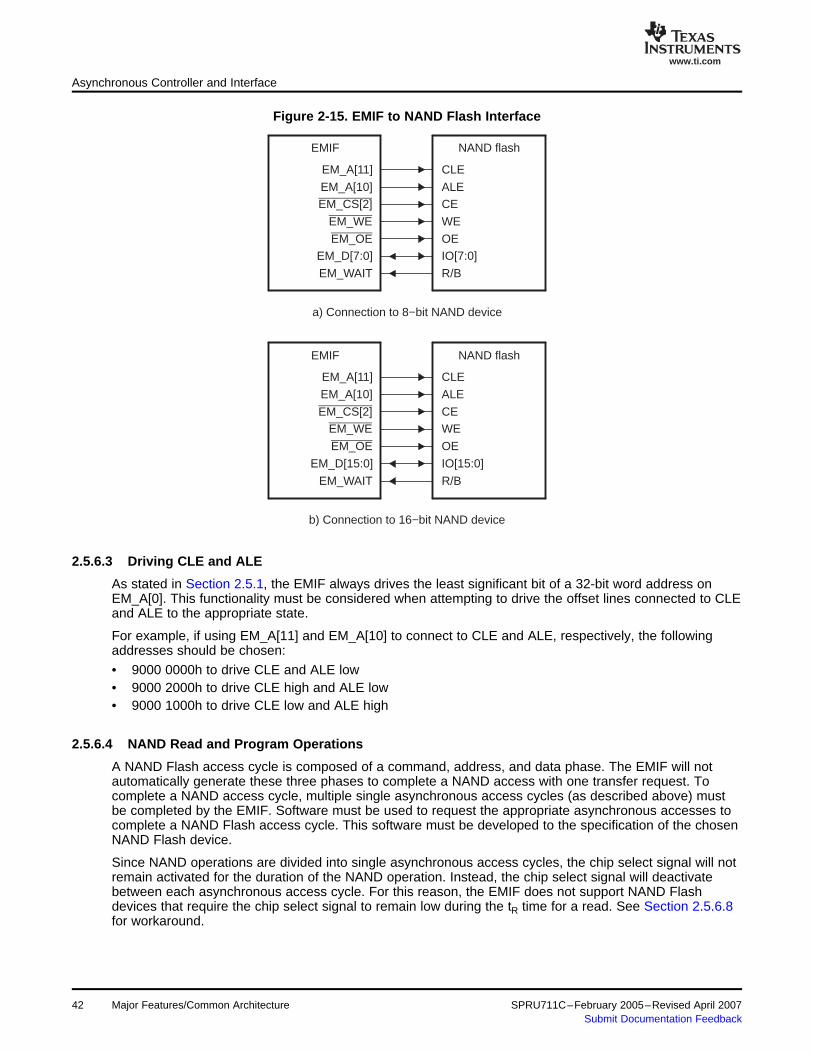
www.ti.com
EM_A[11]
EM_A[10]EM_CS[2]
EM_WE
EM_OEEM_D[7:0]
EM_WAIT
EMIF
CLE
ALECE
WE
OEIO[7:0]
R/B
NAND flash
a) Connection to 8−bit NAND device
b) Connection to 16−bit NAND device
EM_WAIT
EM_D[15:0]
EM_OE
EM_WEEM_CS[2]
EM_A[10]
EM_A[11]
EMIF
CE
IO[15:0]
R/B
OE
WE
NAND flash
CLE
ALE
2.5.6.3 Driving CLE and ALE
2.5.6.4 NAND Read and Program Operations
Asynchronous Controller and Interface
Figure 2-15. EMIF to NAND Flash Interface
As stated in Section 2.5.1, the EMIF always drives the least significant bit of a 32-bit word address onEM_A[0]. This functionality must be considered when attempting to drive the offset lines connected to CLEand ALE to the appropriate state.
For example, if using EM_A[11] and EM_A[10] to connect to CLE and ALE, respectively, the followingaddresses should be chosen:
• 9000 0000h to drive CLE and ALE low• 9000 2000h to drive CLE high and ALE low• 9000 1000h to drive CLE low and ALE high
A NAND Flash access cycle is composed of a command, address, and data phase. The EMIF will notautomatically generate these three phases to complete a NAND access with one transfer request. Tocomplete a NAND access cycle, multiple single asynchronous access cycles (as described above) mustbe completed by the EMIF. Software must be used to request the appropriate asynchronous accesses tocomplete a NAND Flash access cycle. This software must be developed to the specification of the chosenNAND Flash device.
Since NAND operations are divided into single asynchronous access cycles, the chip select signal will notremain activated for the duration of the NAND operation. Instead, the chip select signal will deactivatebetween each asynchronous access cycle. For this reason, the EMIF does not support NAND Flashdevices that require the chip select signal to remain low during the tR time for a read. See Section 2.5.6.8for workaround.
42 Major Features/Common Architecture SPRU711C–February 2005–Revised April 2007Submit Documentation Feedback

www.ti.com
2.5.6.5 NAND Data Read and Write via dMAX
2.5.6.6 ECC Generation
Bit 7Bit 7
Bit 7Bit 7
Bit 6 Bit 5 Bit 4 Bit 3 Bit 2 Bit 1 Bit 0Bit 6 Bit 5 Bit 4 Bit 2Bit 3 Bit 1 Bit 0
Bit 6Bit 6
Bit 1Bit 3 Bit 2Bit 4Bit 5Bit 5 Bit 4 Bit 2Bit 3 Bit 1
Bit 0Bit 0
p8o
p8op8e
p8ep16e
p16op32e
Byte 1Byte 2Byte 3Byte 4
Bit 6Bit 6
Bit 6Bit 6
Byte 2 Bit 7
Byte 4Byte 3
Bit 7Bit 7
Byte 1 Bit 7Bit 1Bit 3 Bit 2Bit 4Bit 5
Bit 5Bit 5 Bit 4
Bit 4 Bit 2Bit 2Bit 3
Bit 3Bit 1Bit 1
Bit 5 Bit 4 Bit 2Bit 3 Bit 1p16e
p8oBit 0
p16oBit 0Bit 0
p8op8e
p32e
Bit 0 p8e
p2048e
p2048o
p1o p1e p1ep1o p1ep1o p1o p1ep2o p2e p2o p2e
p4o p4e
2.5.6.7 NAND Flash Status Register (NANDFSR)
Asynchronous Controller and Interface
Care must be taken when performing a NAND read or write operation via the dMAX controller. SeeSection 2.5.6.5 for more details.
Note: The EMIF does not support NAND Flash devices that require the chip select signal toremain low during the tR time for a read. See Section 2.5.6.8 for workaround.
When performing NAND accesses, the dMAX controller is most efficiently used for the data phase of theaccess. The command and address phases of the NAND access require only a few words of data to betransferred, and therefore do not take advantage of the dMAX controlller's ability to transfer largerquantities of data with a single request.
If the CS2NAND bit in the NAND Flash control register (NANDFCR) is set to 1, the EMIF supports ECCcalculation for up to 512 bytes. To perform the ECC calculation, the CS2ECC bit in NANDFCR must beset to 1. It is the responsibility of the software to start the ECC calculation by writing to the CS2ECC bitprior to issuing a write or read to NAND Flash. It is also the responsibility of the software to read thecalculated ECC from the NAND Flash 1 ECC register (NANDF1ECC) once the transfer to NAND Flashhas completed. If the software writes or reads more than 512 bytes, the ECC will be incorrect. Readingthe NAND2ECC clears the CS2ECC bit in NANDPCR. The NANDF1ECC is cleared upon writing a 1 tothe CS2ECC bit. Figure 2-16 shows the algorithm used to calculate the ECC value for an 8-bit NANDFlash.
For an 8-bit NAND Flash p1o through p4e are column parities and p8e through p2048o are row parities.Similarly, the algorithm can be extended to a 16-bit NAND Flash. For a 16-bit NAND Flash p1o throughp8e are column parities and p16e through p2048o are row parities. The software must ignore theunwanted parity bits if ECC is desired for less than 512 bytes of data. For example. p2048e and p2048oare not required for ECC on 256 bytes of data. Similarly, p1024e, p1024o, p2048e, and p2048o are notrequired for ECC on 128 bytes of data.
Figure 2-16. ECC Value for 8-Bit NAND Flash
The NAND Flash status register (NANDFSR) indicates the raw status of the EM_WAIT pin while in NANDFlash Mode. The EM_WAIT pin should be connected to the NAND Flash device's R/B signal, so that itindicates whether or not the NAND Flash device is busy. During a read, the R/B signal will transition andremain low while the NAND Flash retrieves the data requested. Once the R/B signal transitions high, therequested data is ready and should be read by the EMIF. During a write/program operation, the R/B signal
SPRU711C–February 2005–Revised April 2007 Major Features/Common Architecture 43Submit Documentation Feedback
www.ti.com
2.5.6.8 Interfacing to a Non-CE Don't Care NAND Flash
2.5.7 Extended Wait Mode and the EM_WAIT Pin
Asynchronous Controller and Interface
transitions and remains low while the NAND Flash is programming the Flash with the data it has receivedfrom the EMIF. Once the R/B signal transitions high, the data has been written to the Flash and the nextphase of the transaction may be performed. From this explanation, you can see that the NAND Flashstatus register is useful to the software for indicating the status of the NAND Flash device and determiningwhen to proceed to the next phase of a NAND Flash operation.
When a rising edge occurs on the EM_WAIT pin, the EMIF sets the WR (Wait Rise) bit in the EMIFInterrupt Raw Register (EIRR). Therefore, the EMIF Wait Rise interrupt may be used to indicate the statusof the NAND Flash device. The WP0 bit in the Asynchronous Wait Cycle Configuration Register (AWCCR)does not affect the NAND Flash status register (NANDFSR) or the WR bit in EIRR. See Section 2.8 formore a detailed description of the wait rise interrupt.
As explained in Section 2.5.6.4, the EMIF does not support NAND Flash devices that require the chipselect signal to remain low during the tR time for a read. One way to work around this limitation is to use aGPIO pin to drive the CE signal of the NAND Flash device. If this work around is implemented, softwarewill configure the selected GPIO to be low, then begin the NAND Flash operation, starting with thecommand phase. Once the NAND Flash operation has completed the software can then configure theselected GPIO to be high.
The EMIF on some devices (see the device Data Manual for details) supports the Extend Wait Mode. Thisis a mode in which the external asynchronous device may assert control over the length of the strobeperiod. The Extended Wait Mode can be entered by setting the EW bit in the Asynchronous 1Configuration Register (A1CR). When this bit is set, the EMIF monitors the EM_WAIT pin to determine ifthe attached device wishes to extend the strobe period of the current access cycle beyond theprogrammed number of clock cycles.
When the EMIF detects that the EM_WAIT pin has been asserted, it will begin inserting extra strobecycles into the operation until the EM_WAIT pin is deactivated by the external device. The EMIF will thenreturn to the last cycle of the programmed strobe period and the operation will proceed as usual from thispoint. Please refer to the device data manual for details on the timing requirements of the EM_WAITsignal.
The EM_WAIT pin cannot be used to extend the strobe period indefinitely. The programmable MEWC fieldin the Asynchronous Wait Cycle Configuration Register (AWCCR) determines the maximum number ofEM_CLK cycles the strobe period may be extended beyond the programmed length. When the thecounter expires, the EMIF proceeds to the hold period of the operation regardless of the state of theEM_WAIT pin. The EMIF can also generate an interrupt upon expiration of this counter. See Section 2.8.1for details on enabling this interrupt.
For the EMIF to function properly in the Extended Wait mode, the WP0 bit of AWCCR must beprogrammed to match the polarity of the EM_WAIT pin. In its reset state of 1, the EMIF will insert waitcycles when the EM_WAIT pin is sampled high. When set to 0, the EMIF will insert wait cycles only whenEM_WAIT is sampled low. This programmability allows for a glueless connection to larger variety ofasynchronous devices.
Finally, a restriction is placed on the the strobe period timing parameters when operating in Extended Waitmode. Specifically, the W_STROBE and R_STROBE fields must not be set to 0 for proper operation.
Major Features/Common Architecture44 SPRU711C–February 2005–Revised April 2007Submit Documentation Feedback

www.ti.com
2.6 Data Bus Parking
2.7 Reset and Initialization Considerations
2.8 Interrupt Support
2.8.1 Interrupt Events
Data Bus Parking
The EMIF always drives the data bus to the previous write data value when it is idle. This feature is calleddata bus parking. Only when the EMIF issues a read command to the external memory does it stopdriving the data bus. After the EMIF latches the last read data, it immediately parks the data bus again.
The one exception to this behavior occurs after performing an asynchronous read operation while theEMIF is in the self-refresh state. In this situation, the read operation is not followed by the EMIF parkingthe data bus. Instead, the EMIF tri-states the data bus. Therefore, it is not recommended to performasynchronous read operations while the EMIF is in the self-refresh state, in order to prevent floating inputson the data bus. External pull-ups, such as 10kΩ resistors, should be placed on the lower 16 EMIF databus pins (which do not have internal pull-ups) if it is required to perform reads in this situation. The preciseresistor value should be chosen so that the worst case combined off-state leakage currents do not causethe voltage levels on the associated pins to drop below the high-level input voltage requirement.
More information about the self-refresh state can be found in Section 2.4.7.
The EMIF and its registers will be reset when any of the following events occur:
1. The RESET pin on the device is asserted2. The digital watchdog timer in the RTI peripheral is enabled and times out3. An emulator reset is initiated through Code Composer Studio
In the first two cases, the EMIF will exit the reset state when RESET is released and after the PLLcontroller releases the entire device from reset. In the third case, the EMIF will exit the reset stateimmediately after the emulator reset is complete.
In all three cases, the EMIF automatically begins running the SDRAM initialization sequence described inSection 2.4.4 after coming out of reset. Even though the initialization procedure is automatic, a specialprocedure, found in Section 2.4.5 must still be followed.
The EMIF supports a single interrupt to the CPU. Section 2.8.1 details the generation and internalmasking of EMIF interrupts, and Section 2.8.2 describes how the EMIF interrupts are sent to the CPU.
There are two conditions that may cause the EMIF to generate an interrupt to the CPU. These twoconditions are:• A rising edge on the EM_WAIT signal (wait rise interrupt)• An asynchronous time out
The wait rise interrupt is not affected by the WP0 bit in the asynchronous wait cycle configuration register(AWCCR). The asynchronous time out interrupt condition occurs when the attached asynchronous devicefails to deassert the EM_WAIT pin within the number of cycles defined by the MEWC bit in AWCCR.
Only when the interrupt is enabled by setting the appropriate bit (WRMSET or ATMSET) in the EMIFInterrupt Mask Set Register (EIMSR) to 1, will the interrupt be sent to the CPU. Once enabled, theinterrupt may be disabled by writing a 1 to the corresponding bit in the EMIF Interrupt Mask Clear Register(EIMCR). The bit fields in both the EIMSR and EIMCR may be used to indicate whether the interrupt isenabled. When the interrupt is enabled, the corresponding bit field in both the EIMSR and EIMCR willhave a value of 1; when the interrupt is disabled, the corresponding bit field will have a value of 0.
The EMIF Interrupt Raw Register (EIRR) and the EMIF Interrupt Mask Register (EIMR) indicate the statusof each interrupt. The appropriate bit (WR or AT) in EIRR is set when the interrupt condition occurs,whether or not the interrupt has been enabled. However, the appropriate bit (WRM or ATM) in EIMR is setonly when the interrupt condition occurs and the interrupt is enabled. Writing a 1 to the bit in EIRR clearsthe EIRR bit as well as the corresponding bit in EIMR.Table 2-26 contains a brief summary of the interruptstatus and control bit fields. See Chapter 3 for complete details on the register fields.
SPRU711C–February 2005–Revised April 2007 Major Features/Common Architecture 45Submit Documentation Feedback
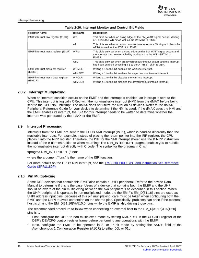
www.ti.com
2.8.2 Interrupt Multiplexing
2.9 Interrupt Processing
2.10 Pin Multiplexing
Interrupt Processing
Table 2-26. Interrupt Monitor and Control Bit Fields
Register Name Bit Name Description
EMIF interrupt raw register (EIRR) WR This bit is set when an rising edge on the EM_WAIT signal occurs. Writinga 1 clears the WR bit as well as the WRM bit in EIMR.
AT This bit is set when an asynchronous timeout occurs. Writing a 1 clears theAT bit as well as the ATM bit in EIMR.
EMIF interrupt mask register (EIMR) WRM This bit is only set when a rising edge on the EM_WAIT signal occurs andthe interrupt has been enabled by writing a 1 to the WRMSET bit inEIMSR.
ATM This bit is only set when an asynchronous timeout occurs and the interrupthas been enabled by writing a 1 to the ATMSET bit in EIMSR.
EMIF interrupt mask set register WRMSET Writing a 1 to this bit enables the wait rise interrupt.(EIMSR) ATMSET Writing a 1 to this bit enables the asynchronous timeout interrupt.
EMIF interrupt mask clear register WRCLR Writing a 1 to this bit disables the wait rise interrupt.(EIMCR) ATMCLR Writing a 1 to this bit disables the asynchronous timeout interrupt.
When an interrupt condition occurs on the EMIF and the interrupt is enabled, an interrupt is sent to theCPU. This interrupt is logically ORed with the non-maskable interrupt (NMI) from the dMAX before beingsent to the CPU NMI Interrupt. The dMAX does not utilize the NMI on all devices. Refer to the dMAXPeripheral Reference Guide for your device to determine if the NMI is used. If the dMAX uses the NMI andthe EMIF enables its interrupt, the ISR for this interrupt needs to be written to determine whether theinterrupt was generated by the dMAX or the EMIF.
Interrupts from the EMIF are sent to the CPU's NMI interrupt (INT1), which is handled differently than themaskable interrupts. For example, instead of placing the return pointer into the IRP register, the CPUplaces it into the NRP register. Therefore, the ISR for the NMI interrupt should use the B NRP instructioninstead of the B IRP instruction to when returning. The NMI_INTERRUPT pragma enables you to handlethe nonmaskable interrupt directly with C code. The syntax for the pragma in C is:
#pragma NMI_INTERRUPT (func);
where the argument "func" is the name of the ISR function.
For more details on the CPU's NMI interrupt, see the TMS320C6000 CPU and Instruction Set ReferenceGuide (SPRU189F).
Some DSP devices that contain this EMIF also contain a UHPI peripheral. Refer to the device DataManual to determine if this is the case. Users of a device that contains both the EMIF and the UHPIshould be aware of the pin multiplexing between the two peripherals as described in this section. Whenthe UHPI peripheral is operated in non-multiplexed mode, the the EMIF's EM_D[31:16] pins are used asUHPI address input pins. Because of this pin multiplexing, care must be taken when configuring both theEMIF and the UHPI to avoid contention on the shared pins. Specifically, problems can arise if the externalhost is driving the EM_D[31:16]/HA[15:0] pins while the EMIF is also driving those pins.
The recommended procedure to follow when connecting an external host to the EM_D[31:16]/HA[15:0]pins is to:• First, configure the UHPI to non-multiplexed mode by setting NMUX = 1 in the CFGHPI register of the
DSP's DEVCFG control register frame before performing any operations with the EMIF.• Next, configure the EMIF to be operated in 8- or 16-bit mode by setting the ASIZE field of the
Asynchronous 1 Configuration Register (A1CR) to either 00b or 01b.
46 Major Features/Common Architecture SPRU711C–February 2005–Revised April 2007Submit Documentation Feedback

www.ti.com
2.11 Priority and Arbitration
2.12 System Considerations
2.12.1 Asynchronous Request Times
Priority and Arbitration
The recommended procedure to follow when an external host will not be connected to theEM_D[31:16]/HA[15:0] pins is to:• Verify that NMUX = 0 in the CFGHPI register of the DSP's DEVCFG control register frame.• Configure the EMIF to any bus width desired.
Section 2.2 of this document describes the external prioritization and arbitration among requests fromdifferent sources within the DSP. The result of this external arbitration is that only one request ispresented to the EMIF at a time. Once the EMIF completes a request, the external arbiter then providesthe EMIF with the next pending request.
Internally, the EMIF undertakes memory device transactions according to a strict priority scheme. Thehighest priority events are:• A device reset.• A write to any of the three least significant bytes of the SDRAM Configuration Register (SDCR).Either of these events will cause the EMIF to immediately commence its initialization sequence asdescribed in Section 2.4.4.
Once the EMIF has completed its initialization sequence, it performs memory transactions according to thefollowing priority scheme (highest priority listed first):
1. If the EMIF's backlog refresh counter is at the Refresh Must urgency level, the EMIF performs multipleSDRAM auto refresh cycles until the Refresh Release urgency level is reached.
2. If an SDRAM or asynchronous read has been requested, the EMIF performs a read operation.3. If the EMIF's backlog refresh counter is at the Refresh Need urgency level, the EMIF performs an
SDRAM auto refresh cycle.4. If an SDRAM or asynchronous write has been requested, the EMIF performs a write operation.5. If the EMIF's backlog refresh counter is at the Refresh May or Refresh Release urgency level, the
EMIF performs an SDRAM auto refresh cycle.6. If the value of the SR bit in SDCR has been set to 1, the EMIF will enter the self-refresh state as
described in Section 2.4.7.
After taking one of the actions listed above, the EMIF then returns to the top of the priority list to determineits next action.
Because the EMIF does not issue auto-refresh cycles when in the self-refresh state, the above priorityscheme does not apply when in this state. See Section 2.4.7 for details on the operation of the EMIF whenin the self-refresh state.
This section describes various system considerations to keep in mind when operating the EMIF.
In a system that interfaces to both SDRAM and asynchronous memory, the asynchronous requests mustnot take longer than the smaller of the following two values:• tRAS (typically 120us) - to avoid violating the maximum time allowed between issuing an ACTV and
PRE command to the SDRAM.• tRefresh Rate * 11 (typically 15.7us * 11 = 172.7us) - to avoid refresh violations on the SDRAM.
The length of an asynchronous request is controlled by multiple factors, the primary factor being thenumber of access cycles required to complete the request. For example, an asynchronous request for4 bytes will require four access cycles using an 8-bit data bus and only one access cycle using a 32-bitdata bus. The maximum request size that the C672x EMIF can be sent is 16 words, therefore themaximum number of access cycles per memory request is 64 when the EMIF is configured with an8-bit data bus. The length of the individual access cycles that make up the asynchronous request is
SPRU711C–February 2005–Revised April 2007 Major Features/Common Architecture 47Submit Documentation Feedback

www.ti.com
2.12.2 Cache Fill Requests
2.13 Power Management
2.14 Emulation Considerations
Power Management
determined by the programmed setup, strobe, hold, and turnaround values, but can also be extendedwith the assertion of the EM_WAIT input signal up to a programmed maximum limit. It is up to the userto make sure that an entire asynchronous request does not exceed the timing values listed abovewhen also interfacing to an SDRAM device. This can be done by limiting the asynchronous timingparameters.
The DSP can run code from either internal or external memory. When running code from externalmemory, the DSP's program cache is periodically filled with eight words (32-bytes) through a dedicatedport to the EMIF. Two system level concerns arise when filling the program cache from the EMIF.
First, the program cache fills have the possibility of being locked out from accessing the EMIF by a streamof higher priority requests. As described in Section 2.2, a program cache fill request through the PMP hasthe lowest priority among all EMIF requestors. Therefore, care should be taken when issuing persistentrequests to the EMIF from a source such as the dMAX.
Second, requests to the EMIF from the other sources such as the dMAX risk missing their deadlines whilea program cache fill from the EMIF is in progress. This is because all other EMIF accesses are heldpending while the program cache is filled through the PMP. The worst-case scenario that can arise iswhen a requester submits a request immediately after a program cache fill request has begun. Thesystem should be analyzed to make sure that this worst-case request delay is acceptable.
The EMIF can be placed into a self-refresh state in order to place the attached SDRAM devices intoself-refresh mode, which consumes less power for most SDRAM devices. In this state, the attachedSDRAM device uses an internal clock to perform its own auto refresh cycles. This maintains the validity ofthe data in the SDRAM without the need for any external commands. Refer to Section 2.4.7 for moredetails on placing the EMIF into the self-refresh state.
The operation of the EMIF is not affected when a breakpoint is reached or an emulation halt occurs.
48 Major Features/Common Architecture SPRU711C–February 2005–Revised April 2007Submit Documentation Feedback

Chapter 3SPRU711C–February 2005–Revised April 2007
Registers
The external memory interface (EMIF) is controlled by programming its internalmemory-mapped registers (MMRs). A list of these registers is provided in the tablebelow. The values on reset are shown below each field name in the register figures.
Note: All EMIFs MMRs, except SDCR, only support word, i.e., 32-bit,accesses. Performing a byte (8-bit) or half-word (16-bit) write tothese register will result in undefined behavior. The SDCR is bytewritable to allow the setting of the SR bit without triggering theSDRAM initialization sequence.
Topic .................................................................................................. Page
3.1 Introduction.............................................................................. 503.2 Asynchronous Wait Cycle Configuration Register (AWCCR) .......... 513.3 SDRAM Configuration Register (SDCR) ....................................... 523.4 SDRAM Refresh Control Register (SDRCR) .................................. 543.5 Asynchronous Configuration Register (A1CR).............................. 553.6 SDRAM Timing Register (SDTIMR) .............................................. 553.7 SDRAM Self Refresh Exit Timing Register (SDSRETR) .................. 573.8 EMIF Interrupt Raw Register (EIRR)............................................. 583.9 EMIF Interrupt Masked Register (EIMR) ....................................... 593.10 EMIF Interrupt Mask Set Register (EIMSR) ................................... 603.11 EMIF Interrupt Mask Clear Register (EIMCR) ................................ 613.12 NAND Flash Control Register (NANDFCR).................................... 623.13 NAND Flash Status Register (NANDFSR) ..................................... 633.14 NAND Flash 1 ECC Register (NANDF1ECC).................................. 63
SPRU711C–February 2005–Revised April 2007 Registers 49Submit Documentation Feedback
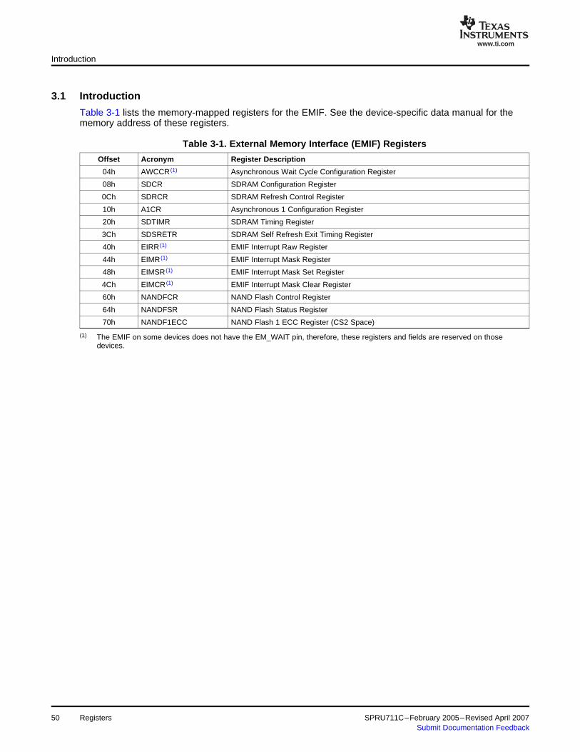
www.ti.com
3.1 Introduction
Introduction
Table 3-1 lists the memory-mapped registers for the EMIF. See the device-specific data manual for thememory address of these registers.
Table 3-1. External Memory Interface (EMIF) Registers
Offset Acronym Register Description
04h AWCCR (1) Asynchronous Wait Cycle Configuration Register
08h SDCR SDRAM Configuration Register
0Ch SDRCR SDRAM Refresh Control Register
10h A1CR Asynchronous 1 Configuration Register
20h SDTIMR SDRAM Timing Register
3Ch SDSRETR SDRAM Self Refresh Exit Timing Register
40h EIRR (1) EMIF Interrupt Raw Register
44h EIMR (1) EMIF Interrupt Mask Register
48h EIMSR (1) EMIF Interrupt Mask Set Register
4Ch EIMCR (1) EMIF Interrupt Mask Clear Register
60h NANDFCR NAND Flash Control Register
64h NANDFSR NAND Flash Status Register
70h NANDF1ECC NAND Flash 1 ECC Register (CS2 Space)
(1) The EMIF on some devices does not have the EM_WAIT pin, therefore, these registers and fields are reserved on thosedevices.
Registers50 SPRU711C–February 2005–Revised April 2007Submit Documentation Feedback
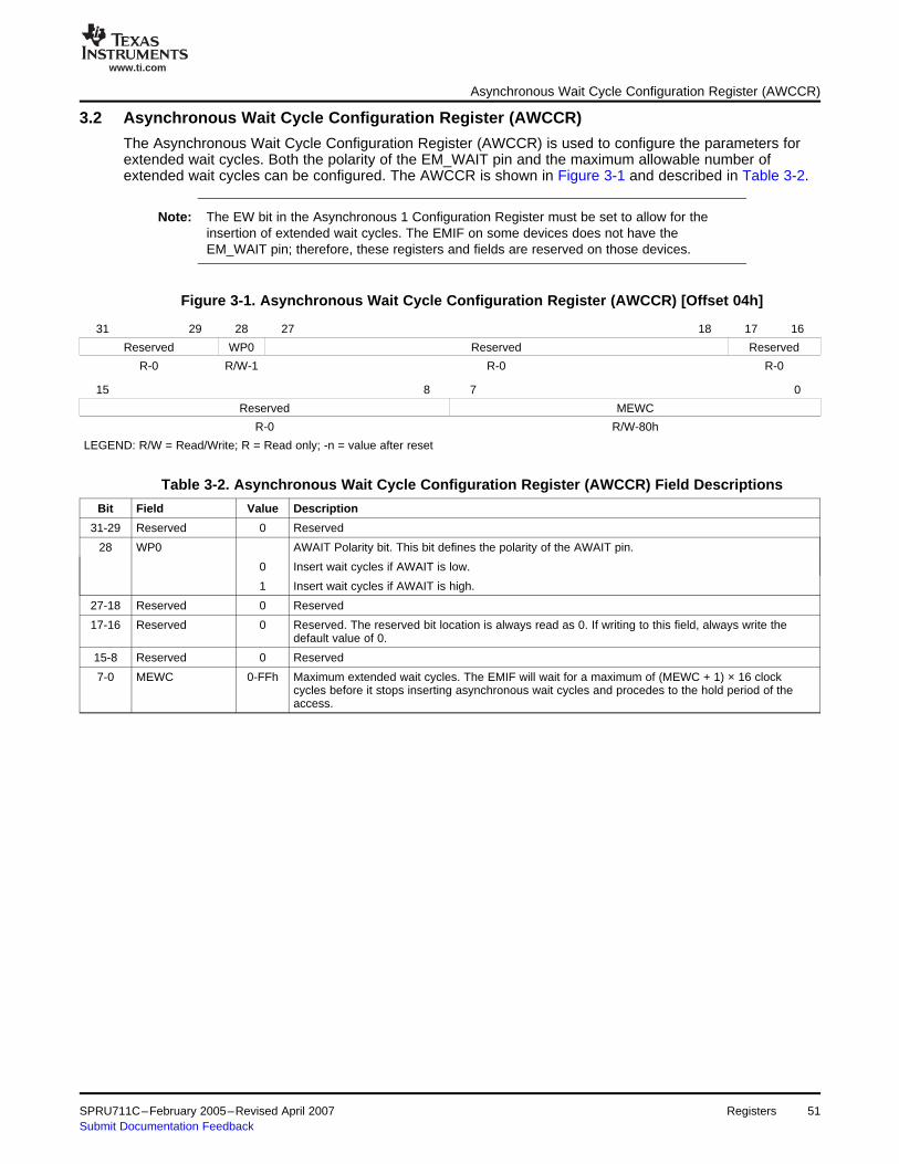
www.ti.com
3.2 Asynchronous Wait Cycle Configuration Register (AWCCR)
Asynchronous Wait Cycle Configuration Register (AWCCR)
The Asynchronous Wait Cycle Configuration Register (AWCCR) is used to configure the parameters forextended wait cycles. Both the polarity of the EM_WAIT pin and the maximum allowable number ofextended wait cycles can be configured. The AWCCR is shown in Figure 3-1 and described in Table 3-2.
Note: The EW bit in the Asynchronous 1 Configuration Register must be set to allow for theinsertion of extended wait cycles. The EMIF on some devices does not have theEM_WAIT pin; therefore, these registers and fields are reserved on those devices.
Figure 3-1. Asynchronous Wait Cycle Configuration Register (AWCCR) [Offset 04h]
31 29 28 27 18 17 16
Reserved WP0 Reserved Reserved
R-0 R/W-1 R-0 R-0
15 8 7 0
Reserved MEWC
R-0 R/W-80h
LEGEND: R/W = Read/Write; R = Read only; -n = value after reset
Table 3-2. Asynchronous Wait Cycle Configuration Register (AWCCR) Field Descriptions
Bit Field Value Description
31-29 Reserved 0 Reserved
28 WP0 AWAIT Polarity bit. This bit defines the polarity of the AWAIT pin.
0 Insert wait cycles if AWAIT is low.
1 Insert wait cycles if AWAIT is high.
27-18 Reserved 0 Reserved
17-16 Reserved 0 Reserved. The reserved bit location is always read as 0. If writing to this field, always write thedefault value of 0.
15-8 Reserved 0 Reserved
7-0 MEWC 0-FFh Maximum extended wait cycles. The EMIF will wait for a maximum of (MEWC + 1) × 16 clockcycles before it stops inserting asynchronous wait cycles and procedes to the hold period of theaccess.
SPRU711C–February 2005–Revised April 2007 Registers 51Submit Documentation Feedback

www.ti.com
3.3 SDRAM Configuration Register (SDCR)
SDRAM Configuration Register (SDCR)
The SDRAM Configuration Register (SDCR) is used to configure various parameters of the SDRAMcontroller such as the number of internal banks, the internal page size, and the CAS latency to matchthose of the attached SDRAM device. In addition, this register is used to put the attached SDRAM deviceinto Self-Refresh mode. The SDCR is shown in Figure 3-2 and described in Table 3-3.
Note: Writing to the lower three bytes of this register will cause the EMIF to start the SDRAMinitialization sequence described in Section 2.4.4.
Figure 3-2. SDRAM Configuration Register (SDCR) [Offset 08h]
31 30 24
SR Reserved
R/W-0 R-0
23 17 16
Reserved Reserved
R-0 R-0
15 14 13 12 11 9 8
Reserved NM Reserved Reserved CL BIT11_9LOCK
R-0 R/W-0 (A) R-0 R-0 R/W-3h R/W-0
7 6 4 3 2 0
Reserved IBANK Reserved PAGESIZE
R-0 R-2h R-0 R/W-0
LEGEND: R/W = Read/Write; R = Read only; -n = value after reset
A This bit field must be set to 1 if the EMIF on your device only has 16 data bus pins.
Table 3-3. SDRAM Configuration Register (SDCR) Field Descriptions
Bit Field Value Description
31 SR Self-Refresh mode bit. This bit controls entering and exiting of the Self-Refresh modedescribed in Section 2.4.7. The field should be written using a byte-write to the upperbyte of SDCR to avoid triggering the SDRAM initialization sequence.
0 Writing a 0 to this bit will cause connected SDRAM devices and the EMIF to exit theSelf-Refresh mode.
1 Writing a 1 to this bit will cause connected SDRAM devices and the EMIF to enter theSelf-Refresh mode.
30-17 Reserved 0 Reserved. The reserved bit location is always read as 0. If writing to this field, alwayswrite the default value of 0.
16 Reserved 0 Reserved. The reserved bit location is always read as 0.
15 Reserved 0 Reserved. The reserved bit location is always read as 0. If writing to this field, alwayswrite the default value of 0.
14 NM Narrow mode bit. This bit defines whether a 16- or 32-bit-wide SDRAM is connectedto the EMIF. This bit field must be set to 1 if the EMIF on your device only has 16data bus pins. Writing to this field triggers the SDRAM initialization sequence.
0 32-bit SDRAM data bus is used.
1 16-bit SDRAM data bus is used.
13 Reserved 0 Reserved. The reserved bit location is always read as 0. If writing to this field, alwayswrite the default value of 0.
12 Reserved 0 Reserved. The reserved bit location is always read as 0. If writing to this field, alwayswrite the default value of 0.
52 Registers SPRU711C–February 2005–Revised April 2007Submit Documentation Feedback

www.ti.com
SDRAM Configuration Register (SDCR)
Table 3-3. SDRAM Configuration Register (SDCR) Field Descriptions (continued)
Bit Field Value Description
11-9 CL 0-7h CAS Latency. This field defines the CAS latency to be used when accessingconnected SDRAM devices. A 1 must be simultaniously written to the BIT11_9LOCKbit field of this register in order to write to the CL bit field. Writing to this field triggersthe SDRAM initialization sequence.
0-1h Reserved
2h CAS latency = 2 EM_CLK cycles
3h CAS latency = 3 EM_CLK cycles
4h-7h Reserved
8 BIT11_9LOCK Bits 11 to 9 lock. CL can only be written if BIT11_9LOCK is simultaniously written witha 1. BIT11_9LOCK is always read as 0. Writing to this field triggers the SDRAMinitialization sequence.
0 CL cannot be written.
1 CL can be written.
7 Reserved 0 Reserved. The reserved bit location is always read as 0. If writing to this field, alwayswrite the default value of 0.
6-4 IBANK Internal SDRAM Bank size. This field defines number of banks inside the connectedSDRAM devices. Writing to this field triggers the SDRAM initialization sequence.
0 1 bank SDRAM devices.
1 2 bank SDRAM devices.
2 4 bank SDRAM devices.
3h-7h Reserved.
3 Reserved 0 Reserved. The reserved bit location is always read as 0. If writing to this field, alwayswrite the default value of 0.
2-0 PAGESIZE 0-7h Page Size. This field defines the internal page size of connected SDRAM devices.Writing to this field triggers the SDRAM initialization sequence.
0 8 column address bits (256 elements per row)
1h 9 column address bits (512 elements per row)
2h 10 column address bits (1024 elements per row)
3h-7h Reserved
SPRU711C–February 2005–Revised April 2007 Registers 53Submit Documentation Feedback

www.ti.com
3.4 SDRAM Refresh Control Register (SDRCR)
SDRAM Refresh Control Register (SDRCR)
The SDRAM Refresh Control Register (SDRCR) is used to configure the rate at which connected SDRAMdevices will be automatically refreshed by the EMIF. Refer to Section 2.4.6 on the refresh controller formore details. The SDRCR is shown in Figure 3-3 and described in Table 3-4.
Figure 3-3. SDRAM Refresh Control Register (SDRCR) [Offset 0Ch]
31 16
Reserved
R-0
15 13 12 0
Reserved RR
R-0 R/W-0190h
LEGEND: R/W = Read/Write; R = Read only; -n = value after reset
Table 3-4. SDRAM Refresh Control Register (SDRCR) Field Descriptions
Bit Field Value Description
31-16 Reserved 0 Reserved. The reserved bit location is always read as 0. If writing to this field, always write thedefault value of 0.
12-0 RR 0-1FFFh Refresh Rate. This field is used to define the SDRAM refresh period in terms of EM_CLKcycles. Writing a value <0010h to this field will cause it to be loaded with the value 0190h.
Registers54 SPRU711C–February 2005–Revised April 2007Submit Documentation Feedback

www.ti.com
3.5 Asynchronous Configuration Register (A1CR)
3.6 SDRAM Timing Register (SDTIMR)
Asynchronous Configuration Register (A1CR)
The Asynchronous 1 Configuration Register (A1CR) is used to configure the shaping of the address andcontrol signals during an access to asynchronous memory. It is also used to program the width ofasynchronous interface and to select from various modes of operation. This register can be written prior toany transfer, and any asynchronous transfer following the write will use the new configuration.The A1CRis shown in Figure 3-4 and described in Table 3-5.
Figure 3-4. Asynchronous 1 Configuration Register (A1CR) [Offset 10h]
31 30 29 26 25 24
SS EW (A) W_SETUP W_STROBE
R/W-0 R/W-0 R/W-Fh R/W-3Fh
23 20 19 17 16
W_STROBE W_HOLD R_SETUP
R/W-3Fh R/W-7h R/W-Fh
15 13 12 7 6 4 3 2 1 0
R_SETUP R_STROBE R_HOLD TA ASIZE
R/W-Fh R/W-3Fh R/W-7h R/W-3h R/W-0
LEGEND: R/W = Read/Write; R = Read only; -n = value after reset
A The EW bit must be cleared to 0 when operating in NAND Flash mode.
B This bit field must be set to 0 if the EMIF on your device does not have an EM_WAIT pin.
Table 3-5. Asynchronous 1 Configuration Register (A1CR) Field Descriptions
Bit Field Value Description
31 SS Select Strobe bit. This bit defines whether the asynchronous interface operates in WE Strobe Modeor Select Strobe Mode. See Section 2.5 for details on the two modes of operation.
0 WE Strobe Mode enabled.
1 Select Strobe Mode enabled.
30 EW Extend Wait bit. This bit defines whether extended wait cycles will be enabled. See Section 2.5.7 onextended wait cycles for details. This bit field must be set to 0 if the EMIF on your device does nothave an EM_WAIT pin.
0 Extended wait cycles disabled.
1 Extended wait cycles enabled.
29-26 W_SETUP 0-Fh Write setup width in EM_CLK cycles, minus one cycle. See Section 2.5.3 for details.
25-20 W_STROBE 0-3Fh Write strobe width in EM_CLK cycles, minus one cycle. See Section 2.5.3 for details.
19-17 W_HOLD 0-7h Write hold width in EM_CLK cycles, minus one cycle. See Section 2.5.3 for details.
16-13 R_SETUP 0-Fh Read setup width in EM_CLK cycles, minus one cycle. See Section 2.5.3 for details.
12-7 R_STROBE 0-3Fh Read strobe width in EM_CLK cycles, minus one cycle. See Section 2.5.3 for details.
6-4 R_HOLD 0-7h Read hold width in EM_CLK cycles, minus one cycle. See Section 2.5.3 for details.
3-2 TA 0-3h Minimum Turn-Around time. This field defines the minimum number of EM_CLK cycles betweenreads and writes, minus one cycle. See Section 2.5.3 for details.
1-0 ASIZE 0-3h Asynchronous Data Bus Width. This field defines the width of the asynchronous device's data bus.
0 8-bit data bus
1h 16-bit data bus
2h 32-bit data bus. Reserved on devices with only 16 EM_D pins.
3h Reserved
The SDRAM Timing Register (SDTIMR) is used to program many of the SDRAM timing parameters.Consult the SDRAM datasheet for information on the appropriate values to program into each field. TheSDTIMR is shown in Figure 3-5 and described in Table 3-6.
SPRU711C–February 2005–Revised April 2007 Registers 55Submit Documentation Feedback

www.ti.com
SDRAM Timing Register (SDTIMR)
Figure 3-5. SDRAM Timing Register (SDTIMR) [Offset 20h]
31 27 26 24 23 22 20 19 18 16
T_RFC T_RP Resv T_RCD Resv T_WR
R/W-0 R/W-0 R-0 R/W-2h R-0 R/W-1h
15 12 11 8 7 6 4 3 0
T_RAS T_RC Resv T_RRD Reserved
R/W-Ch R/W-Fh R-0 R/W-0 R-0
LEGEND: R/W = Read/Write; R = Read only; -n = value after reset
Table 3-6. SDRAM Timing Register (SDTIMR) Field Descriptions
Bit Field Value Description
31-27 T_RFC 0-1Fh Specifies the Trfc value of the SDRAM. This defines the minimum number of EM_CLK cycles fromRefresh (REFR) to Refresh (REFR), minus 1:T_RFC = (Trfc/tEM_CLK) - 1
26-24 T_RP 0-7h Specifies the Trp value of the SDRAM. This defines the minimum number of EM_CLK cycles fromPrecharge (PRE) to Activate (ACTV) or Refresh (REFR) command, minus 1:T_RP = (Trp/tEM_CLK) - 1
23 Reserved 0 Reserved. The reserved bit location is always read as 0. If writing to this field, always write thedefault value of 0.
22-20 T_RCD 0-7h Specifies the Trcd value of the SDRAM. This defines the minimum number of EM_CLK cycles fromActive (ACTV) to Read (READ) or Write (WRT), minus 1:T_RCD = (Trcd/tEM_CLK) - 1
19 Reserved 0 Reserved. The reserved bit location is always read as 0. If writing to this field, always write thedefault value of 0.
18-16 T_WR 0-7h Specifies the Twr value of the SDRAM. This defines the minimum number of EM_CLK cycles fromlast Write (WRT) to Precharge (PRE), minus 1:T_WR = (Twr/tEM_CLK) - 1
15-12 T_RAS 0-Fh Specifies the Tras value of the SDRAM. This defines the minimum number of EM_CLK clock cyclesfrom Activate (ACTV) to Precharge (PRE), minus 1:T_RAS = (Tras/tEM_CLK) - 1
11-8 T_RC 0-Fh Specifies the Trc value of the SDRAM. This defines the minimum number of EM_CLK clock cyclesfrom Activate (ACTV) to Activate (ACTV), minus 1:T_RC = (Trc/tEM_CLK) - 1
7 Reserved 0 Reserved. The reserved bit location is always read as 0. If writing to this field, always write thedefault value of 0.
6-4 T_RRD 0-7h Specifies the Trrd value of the SDRAM. This defines the minimum number of EM_CLK clock cyclesfrom Activate (ACTV) to Activate (ACTV) for a different bank, minus 1:T_RRD = (Trrd/tEM_CLK) - 1
3-0 Reserved 0 Reserved. The reserved bit location is always read as 0. If writing to this field, always write thedefault value of 0.
Registers56 SPRU711C–February 2005–Revised April 2007Submit Documentation Feedback

www.ti.com
3.7 SDRAM Self Refresh Exit Timing Register (SDSRETR)
SDRAM Self Refresh Exit Timing Register (SDSRETR)
The SDRAM Self Refresh Exit Timing Register (SDSRETR) is used to program the amount of timebetween when the SDRAM exits Self-Refresh mode and when the EMIF issues another command. TheSDSRETR is shown in Figure 3-6 and described in Table 3-7.
Figure 3-6. SDRAM Self Refresh Exit Timing Register (SDSRETR) [Offset 3Ch]
31 16
Reserved
R-0
15 5 4 0
Reserved T_XS
R-0 R/W-19h
LEGEND: R/W = Read/Write; R = Read only; -n = value after reset
Table 3-7. SDRAM Self Refresh Exit Timing Register (SDSRETR) Field Descriptions
Bit Field Value Description
31-5 Reserved 0 Reserved. The reserved bit location is always read as 0.
4-0 T_XS 0-1Fh This field specifies the minimum number of ECLKOUT cycles from Self-Refresh exit to anycommand, minus one.T_XS = Txsr / tEM_CLK - 1
SPRU711C–February 2005–Revised April 2007 Registers 57Submit Documentation Feedback

www.ti.com
3.8 EMIF Interrupt Raw Register (EIRR)
EMIF Interrupt Raw Register (EIRR)
The EMIF Interrupt Raw Register (EIRR) is used to monitor and clear the EMIF’s hardware-generatedAsynchronous Timeout Interrupt. The AT bit in this register will be set when an Asynchronous Timeoutoccurs regardless of the status of the Interrupt Mask Set Register and Interrupt Mast Clear Register.Writing a 1 to this bit will clear it. The EMIF on some devices does not have the EM_WAIT pin; therefore,these registers and fields are reserved on those devices. The EIRR is shown in Figure 3-7 and describedin Table 3-8.
Figure 3-7. EMIF Interrupt Raw Register (EIRR) [Offset 40h]
31 8
Reserved
R-0
7 3 2 1 0
Reserved WR Reserved AT
R-0 R/W1C-0 R-0 R/W1C-0
LEGEND: R/W = Read/Write; R = Read only; W1C = Write 1 to clear (writing 0 has no effect); -n = value after reset
Table 3-8. EMIF Interrupt Raw Register (EIRR) Field Descriptions
Bit Field Value Description
31-3 Reserved 0 Reserved. The reserved bit location is always read as 0. If writing to this field, always write thedefault value of 0.
2 WR Wait Rise. This bit is set to 1 by hardware to indicate that a rising edge on the EM_WAIT pin hasoccurred.
0 Indicates that a rising edge has not occurred on the EM_WAIT pin. Writing a 0 has no effect.
1 Indicates that a rising edge has occurred on the EM_WAIT pin. Writing a 1 will clear this bit and theWRM bit in the EMIF interrupt mask register (EIMR).
1 Reserved 0 Reserved. The reserved bit location is always read as 0. If writing to this field, always write thedefault value of 0.
0 AT Asynchronous Timeout. This bit is set to 1 by hardware to indicate that during an extendedasynchronous memory access cycle, the EM_WAIT pin did not go inactive within the number ofcycles defined by the MEWC field in Async Wait Cycle Config Register (AWCCR).
0 Indicates that an Asynchronous Timeout has not occurred. Writing a 0 has no effect.
1 Indicates that an Asynchronous Timeout has occurred. Writing a 1 will clear this bit as well as theATM bit in the EMIF Interrupt Masked Register (EIMM).
Registers58 SPRU711C–February 2005–Revised April 2007Submit Documentation Feedback
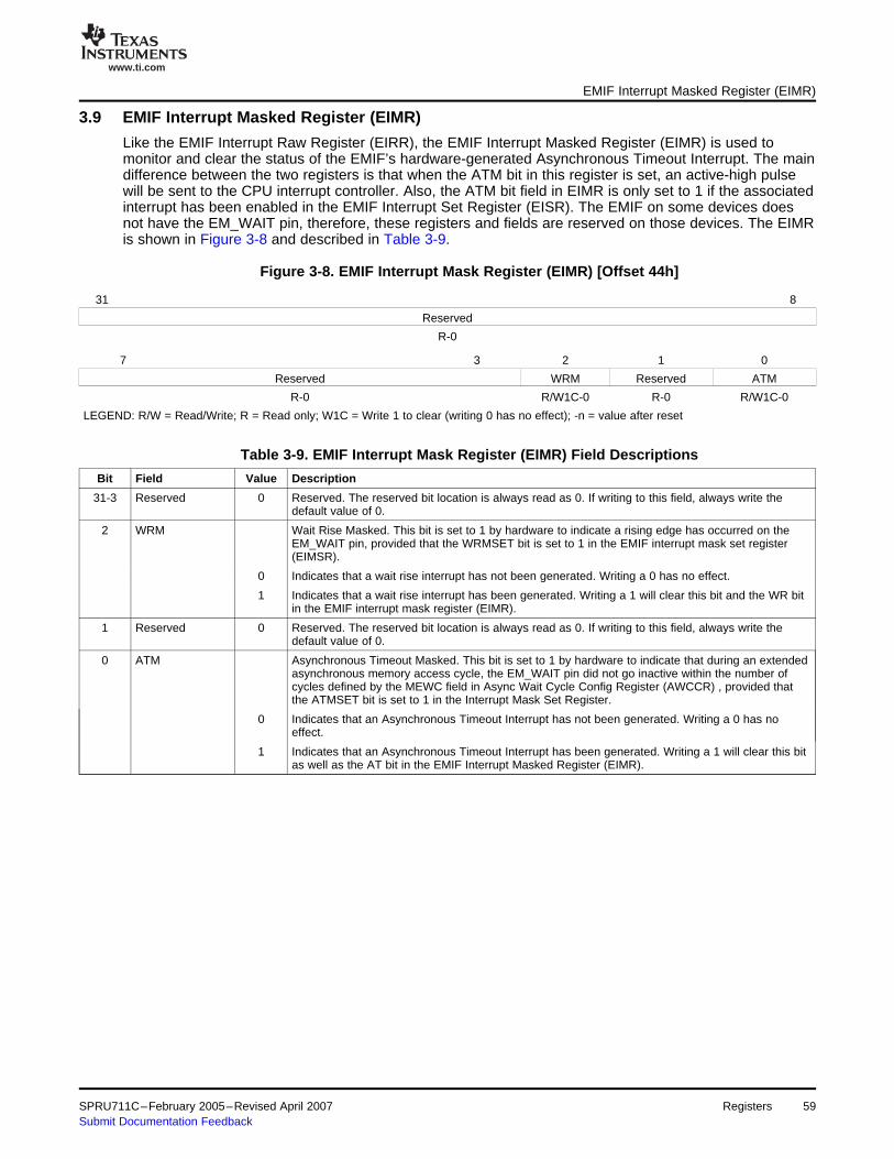
www.ti.com
3.9 EMIF Interrupt Masked Register (EIMR)
EMIF Interrupt Masked Register (EIMR)
Like the EMIF Interrupt Raw Register (EIRR), the EMIF Interrupt Masked Register (EIMR) is used tomonitor and clear the status of the EMIF’s hardware-generated Asynchronous Timeout Interrupt. The maindifference between the two registers is that when the ATM bit in this register is set, an active-high pulsewill be sent to the CPU interrupt controller. Also, the ATM bit field in EIMR is only set to 1 if the associatedinterrupt has been enabled in the EMIF Interrupt Set Register (EISR). The EMIF on some devices doesnot have the EM_WAIT pin, therefore, these registers and fields are reserved on those devices. The EIMRis shown in Figure 3-8 and described in Table 3-9.
Figure 3-8. EMIF Interrupt Mask Register (EIMR) [Offset 44h]
31 8
Reserved
R-0
7 3 2 1 0
Reserved WRM Reserved ATM
R-0 R/W1C-0 R-0 R/W1C-0
LEGEND: R/W = Read/Write; R = Read only; W1C = Write 1 to clear (writing 0 has no effect); -n = value after reset
Table 3-9. EMIF Interrupt Mask Register (EIMR) Field Descriptions
Bit Field Value Description
31-3 Reserved 0 Reserved. The reserved bit location is always read as 0. If writing to this field, always write thedefault value of 0.
2 WRM Wait Rise Masked. This bit is set to 1 by hardware to indicate a rising edge has occurred on theEM_WAIT pin, provided that the WRMSET bit is set to 1 in the EMIF interrupt mask set register(EIMSR).
0 Indicates that a wait rise interrupt has not been generated. Writing a 0 has no effect.
1 Indicates that a wait rise interrupt has been generated. Writing a 1 will clear this bit and the WR bitin the EMIF interrupt mask register (EIMR).
1 Reserved 0 Reserved. The reserved bit location is always read as 0. If writing to this field, always write thedefault value of 0.
0 ATM Asynchronous Timeout Masked. This bit is set to 1 by hardware to indicate that during an extendedasynchronous memory access cycle, the EM_WAIT pin did not go inactive within the number ofcycles defined by the MEWC field in Async Wait Cycle Config Register (AWCCR) , provided thatthe ATMSET bit is set to 1 in the Interrupt Mask Set Register.
0 Indicates that an Asynchronous Timeout Interrupt has not been generated. Writing a 0 has noeffect.
1 Indicates that an Asynchronous Timeout Interrupt has been generated. Writing a 1 will clear this bitas well as the AT bit in the EMIF Interrupt Masked Register (EIMR).
SPRU711C–February 2005–Revised April 2007 Registers 59Submit Documentation Feedback

www.ti.com
3.10 EMIF Interrupt Mask Set Register (EIMSR)
EMIF Interrupt Mask Set Register (EIMSR)
The EMIF Interrupt Mask Set Register (EIMSR) is used to enable the Asynchronous Timeout Interrupt. Ifread as 1, the ATM bit in the EMIF Interrupt Masked Register (EIMR) will be set and an interrupt will begenerated when an Asynchronous Timeout occurs. If read as 0, the ATM bit will always read 0 and nointerrupt will be generated when an Asynchronous Timeout occurs. Writing a 1 to the ATMSET bit enablesthe Asynchronous Timeout Interrupt. The EMIF on some devices does not have the EM_WAIT pin;therefore, these registers and fields are reserved on those devices. The EIMSR is shown in Figure 3-9and described in Table 3-10.
Figure 3-9. EMIF Interrupt Mask Set Register (EIMSR) [Offset 48h]
31 16
Reserved
R-0
15 3 2 1 0
Reserved WRMSET Reserved ATMSET
R-0 R/W-0 R-0 R/W-0
LEGEND: R/W = Read/Write; R = Read only; -n = value after reset
Table 3-10. EMIF Interrupt Mask Set Register (EIMSR) Field Descriptions
Bit Field Value Description
31-3 Reserved 0 Reserved. The reserved bit location is always read as 0. If writing to this field, always write thedefault value of 0.
2 WRMSET Wait Rise Mask Set. This bit determines whether or not the wait rise Interrupt is enabled. Writing a1 to this bit sets this bit, sets the WRMCLR bit in the EMIF interrupt mask clear register (EIMCR),and enables the wait rise interrupt. To clear this bit, a 1 must be written to the WRMCLR bit inEIMCR.
0 Indicates that the wait rise interrupt is disabled. Writing a 0 has no effect.
1 Indicates that the wait rise interrupt is enabled. Writing a 1 sets this bit and the WRMCLR bit in theEMIF interrupt mask clear register (EIMCR).
1 Reserved 0 Reserved. The reserved bit location is always read as 0. If writing to this field, always write thedefault value of 0.
0 ATMSET Asynchronous Timeout Mask Set. This bit determines whether or not the Asynchronous TimeoutInterrupt is enabled. Writing a 1 to this bit sets this bit, sets the ATMCLR bit in the EMIF InterruptMask Clear Register (EIMCR), and enables the Asynchronous Timeout Interrupt. To clear this bit, a1 must be written to the ATMCLR bit of the EMIF Interrupt Mask Clear Register (EIMCR).
0 Indicates that the Asynchronous Timeout Interrupt is disabled. Writing a 0 has no effect.
1 Indicates that the Asynchronous Timeout Interrupt is enabled. Writing a 1 sets this bit and theATMCLR bit in the EMIF Interrupt Mask Clear Register (EIMCR).
Registers60 SPRU711C–February 2005–Revised April 2007Submit Documentation Feedback

www.ti.com
3.11 EMIF Interrupt Mask Clear Register (EIMCR)
EMIF Interrupt Mask Clear Register (EIMCR)
The EMIF Interrupt Mask Clear Register (EIMCR) is used to disable the Asynchronous Timeout Interrupt.If read as 1, the ATM bit in the EMIF Interrupt Masked Register (EIMR) will be set and an interrupt will begenerated when an Asynchronous Timeout occurs. If read as 0, the ATM bit will always read 0 and nointerrupt will be generated when an Asynchronous Timeout occurs. Writing a 1 to the ATMCLR bitdisables the Asynchronous Timeout Interrupt. The EMIF on some devices does not have the EM_WAITpin, therefore, these registers and fields are reserved on those devices. The EIMCR is shown inFigure 3-10 and described in Table 3-11.
Figure 3-10. EMIF Interrupt Mask Clear Register (EIMCR) [Offset 4Ch]
31 16
Reserved
R-0
15 3 2 1 0
Reserved WRMCLR Reserved ATMCLR
R-0 R/W-0 R-0 R/W-0
LEGEND: R/W = Read/Write; R = Read only; -n = value after reset
Table 3-11. EMIF Interrupt Mask Clear Register (EIMCR) Field Descriptions
Bit Field Value Description
31-3 Reserved 0 Reserved. The reserved bit location is always read as 0. If writing to this field, always write thedefault value of 0.
2 WRMCLR Wait Rise Mask Clear. This bit determines whether or not the wait rise interrupt is enabled. Writinga 1 to this bit clears this bit, clears the WRMSET bit in the EMIF interrupt mask set register(EIMSR), and disables the wait rise interrupt. To set this bit, a 1 must be written to the WRMSET bitin EIMSR.
0 Indicates that the wait rise interrupt is disabled. Writing a 0 has no effect.
1 Indicates that the wait rise interrupt is enabled. Writing a 1 clears this bit and the WRMSET bit inthe EMIF interrupt mask set register (EIMSR).
1 Reserved 0 Reserved. The reserved bit location is always read as 0. If writing to this field, always write thedefault value of 0.
0 ATMCLR Asynchronous Timeout Mask Clear. This bit determines whether or not the Asynchronous TimeoutInterrupt is enabled. Writing a 1 to this bit clears this bit, clears the ATMSET bit in the EMIFInterrupt Mask Set Register (EIMSR), and disables the Asynchronous Timeout Interrupt. To set thisbit, a 1 must be written to the ATMSET bit of the EMIF Interrupt Mask Set Register (EIMSR).
0 Indicates that the Asynchronous Timeout Interrupt is disabled. Writing a 0 has no effect.
1 Indicates that the Asynchronous Timeout Interrupt is enabled. Writing a 1 clears this bit and theATMSET bit in the EMIF Interrupt Mask Set Register (EIMSR).
SPRU711C–February 2005–Revised April 2007 Registers 61Submit Documentation Feedback

www.ti.com
3.12 NAND Flash Control Register (NANDFCR)
NAND Flash Control Register (NANDFCR)
The NAND Flash control register (NANDFCR) is shown in Figure 3-11 and described in Table 3-12.
Figure 3-11. NAND Flash Control Register (NANDFCR)
31 16
Reserved
R-0
15 9 8
Reserved CS2ECC
R-0 R/W-0
7 1 0
Reserved CS2NAND
R-0 R/W-0
LEGEND: R/W = Read/Write; R = Read only; -n = value after reset
Table 3-12. NAND Flash Control Register (NANDFCR) Field Descriptions
Bit Field Value Description
31-9 Reserved 0 Reserved
8 CS2ECC NAND Flash ECC start for chip select 2.
0 Do not start ECC calculation.
1 Start ECC calculation on data for NAND Flash on EM_CS2.
7-1 Reserved 0 Reserved
0 CS2NAND NAND Flash mode for chip select 2.
0 Not using NAND Flash.
1 Using NAND Flash on EM_CS2.
Registers62 SPRU711C–February 2005–Revised April 2007Submit Documentation Feedback

www.ti.com
3.13 NAND Flash Status Register (NANDFSR)
3.14 NAND Flash 1 ECC Register (NANDF1ECC)
NAND Flash Status Register (NANDFSR)
The NAND Flash status register (NANDFSR) is shown in Figure 3-12 and described in Table 3-13.
Figure 3-12. NAND Flash Status Register (NANDFSR)
31 16
Reserved
R-0
15 1 0
Reserved WAITST
R-0 R-0
LEGEND: R = Read only; -n = value after reset
Table 3-13. NAND Flash Status Register (NANDFSR) Field Descriptions
Bit Field Value Description
31-1 Reserved 0 Reserved
0 WAITST 0-1h Raw status of the EM_WAIT input pin. The WP0 bit in the asynchronous wait cycle configurationregister (AWCCR) has no effect on WAITST.
The NAND Flash 1 ECC register (NANDF1ECC) is shown in Figure 3-13 and described in Table 3-14. For8-bit NAND Flash, the P1 to P4 bits are column parities; the P8 to P2048 bits are row parities. For 16-bitNAND Flash, the P1 through P8 bits are column parities; the P16 to P2048 bits are row parities.
Figure 3-13. NAND Flash 1 ECC Register (NANDF1ECC)
31 28 27 26 25 24
Reserved P2048O P1024O P512O P256O
R-0 R-0 R-0 R-0 R-0
23 22 21 20 19 18 17 16
P128O P64O P32O P16O P8O P4O P2O P1O
R-0 R-0 R-0 R-0 R-0 R-0 R-0 R-0
15 12 11 10 9 8
Reserved P2048E P1024E P512E P256E
R-0 R-0 R-0 R-0 R-0
7 6 5 4 3 2 1 0
P128E P64E P32E P16E P8E P4E P2E P1E
R-0 R-0 R-0 R-0 R-0 R-0 R-0 R-0
LEGEND: R = Read only; -n = value after reset
Table 3-14. NAND Flash 1 ECC Register (NANDF1ECC) Field Descriptions
Bit Field Value Description
31-28 Reserved 0 Reserved
27 P2048O 0-1 ECC code calculated while reading/writing NAND Flash.
26 P1024O 0-1 ECC code calculated while reading/writing NAND Flash.
25 P512O 0-1 ECC code calculated while reading/writing NAND Flash.
24 P256O 0-1 ECC code calculated while reading/writing NAND Flash.
23 P128O 0-1 ECC code calculated while reading/writing NAND Flash.
22 P64O 0-1 ECC code calculated while reading/writing NAND Flash.
SPRU711C–February 2005–Revised April 2007 Registers 63Submit Documentation Feedback

www.ti.com
NAND Flash 1 ECC Register (NANDF1ECC)
Table 3-14. NAND Flash 1 ECC Register (NANDF1ECC) Field Descriptions (continued)
Bit Field Value Description
21 P32O 0-1 ECC code calculated while reading/writing NAND Flash.
20 P16O 0-1 ECC code calculated while reading/writing NAND Flash.
19 P8O 0-1 ECC code calculated while reading/writing NAND Flash.
18 P4O 0-1 ECC code calculated while reading/writing NAND Flash.
17 P2O 0-1 ECC code calculated while reading/writing NAND Flash.
16 P1O 0-1 ECC code calculated while reading/writing NAND Flash.
15-12 Reserved 0 Reserved
11 P2948E 0-1 ECC code calculated while reading/writing NAND Flash.
10 P102E 0-1 ECC code calculated while reading/writing NAND Flash.
9 P512E 0-1 ECC code calculated while reading/writing NAND Flash.
8 P256E 0-1 ECC code calculated while reading/writing NAND Flash.
7 P128E 0-1 ECC code calculated while reading/writing NAND Flash.
6 P64E 0-1 ECC code calculated while reading/writing NAND Flash.
5 P32E 0-1 ECC code calculated while reading/writing NAND Flash.
4 P15E 0-1 ECC code calculated while reading/writing NAND Flash.
3 P8E 0-1 ECC code calculated while reading/writing NAND Flash.
2 P4E 0-1 ECC code calculated while reading/writing NAND Flash.
1 P2E 0-1 ECC code calculated while reading/writing NAND Flash.
0 P1E 0-1 ECC code calculated while reading/writing NAND Flash.
Registers64 SPRU711C–February 2005–Revised April 2007Submit Documentation Feedback
Chapter 4SPRU711C–February 2005–Revised April 2007
Example Configuration
This chapter presents an example of interfacing the EMIF to both an SDR SDRAMdevice and an asynchronous flash device.
Topic .................................................................................................. Page
4.1 Hardware Interface .................................................................... 664.2 SW Configuration...................................................................... 67
SPRU711C–February 2005–Revised April 2007 Example Configuration 65Submit Documentation Feedback

www.ti.com
4.1 Hardware Interface
EM_CS[0]
EM_CAS
EM_RAS
EM_WE
EM_CLK
EM_CKE
EM_BA[1:0]
EM_A[11:0]
EM_WE_DQM[0]
EM_WE_DQM[1]
EM_D[15:0]
EM_CS[2]
EM_OE
GPIO(6 pins)RESET
EMIF
CE
CAS
RAS
WE
CLK
CKE
BA[1:0]
A[11:0]
LDQM
UDQM
DQ[15:0]
SDRAM1M x 16x 4 bank
A[0]
A[12:1]
DQ[15:0]
CE
WE
OE
RESET
A[18:13]
RY/BY
BYTE
FLASH512K x 16
RESET
VCC
EM_BA[1]
Any GPIO capable pins whichcan be pulled down at resetcan be used to controlA[18:13] for FLASH BOOTLOADExample: AHCLKR0,SPIO_SCS/SCL1
Hardware Interface
Figure 4-1 shows the hardware interface between the EMIF, a Samsung K4S641632H-TC(L)70 64MbSDRAM device, and a SHARP LH28F800BJE-PTTL90 8Mb Flash memory. The connection between theEMIF and the SDRAM is straightforward, but the connection between the EMIF and the flash deserves adetailed look.
The address inputs for the flash are provided by three sources. The A[12:0] address inputs are providedby a combination of the EM_A and EM_BA pins according to Section 2.5.1. The upper address inputsA[18:13] are provided by GPIO pins. The six GPIO pins are connected to the upper address bits of theflash memory and attached to pulldown resistors so that their value is '0' after reset and before configuringthe pins as GPIO. This is necessary if the ROM bootloader is copying the secondary bootloader from theflash. More details on using GPIO pins as upper address pins can be found in Section 2.5.2.
The BYTE input of the flash is tied high to select a 16-bit data bus, and the RY/BY# output from the flashis not used in this example to determine the status of the flash. It is instead asssumed that a pollingmethod will be used when programming and erasing the flash. Finally, this example configurationconnects the EM_WE pin to the WE input of the flash and operates the EMIF in Select Strobe Mode.
Figure 4-1. Example Configuration Interface
Example Configuration66 SPRU711C–February 2005–Revised April 2007Submit Documentation Feedback

www.ti.com
4.2 SW Configuration
4.2.1 Configuring the SDRAM Interface
4.2.1.1 PLL Programming for the EMIF to K4S641632H-TC(L)70 Interface
4.2.1.2 SDRAM Timing Register (SDTIMR) settings for the EMIF to K4S641632H-TC(L)70 Interface
SW Configuration
The following sections describe how to configure the EMIF registers and bit fields to interface the EMIFwith the Samsung K4S641632H-TC(L)70 SDRAM and the SHARP LH28F800BJE-PTTL90 8Mb Flashmemory.
This section describes how to configure the EMIF to interface with the Samsung K4S641632H-TC(L)70SDRAM with a clock frequency of fEM_CLK = 100 MHz. Procedure A described in Section 2.4.5 is followedwhich assumes that the SDRAM power-up timing constraint were met during the SDRAMAuto-Initialization sequence after Reset.
The device PLL Controller should first be programmed to select the desired EM_CLK frequency. Beforedoing this, the SDRAM should be placed into Self-Refresh Mode by setting the SR bit in SDCR. The SRbit should be set using a byte-write to the upper byte of the SDCR to avoid triggering the SDRAMInitialization Sequence. The EM_CLK frequency can now be adjusted to the desired value byprogramming the SYSCLK3 domain of the PLL Controller. Once the PLL has been reprogrammed,remove the SDRAM from Self-Refrsh by clearing the SR bit in SDCR, again with a byte-write.
Table 4-1. SR Field Value For the EMIF to K4S641632H-TC(L)70 Interface
Field Value Purpose
SR 1b then 0b To place the EMIF into the self refresh state
The fields of SDTIMR should be programmed first as described in Table 4-2 to satisfy the required timingparameters for the K4S641632H-TC(L)70. Based on these calculations, a value of 0x61114610 should bewritten to SDTIMR. Figure 4-2 shows a graphical description of how SDTIMR should be programmed.
Table 4-2. SDTIMR Field Calculations for the EMIF to K4S641632H-TC(L)70 Interface
Value from MT48LC4M16A2-75 Value Calculated forField Name Formula Datasheet Field
T_RFC T_RFC >= (tRFC*fEM_CLK) - 1 tRC = 68 ns (min) (1) 6
T_RP T_RP >= (tRP*fEM_CLK) - 1 tRP = 20 ns (min) 1
T_RCD T_RCD >= (tRCD*fEM_CLK) - 1 tRCD = 20 ns (min) 1
T_WR T_WR >= (tWR*fEM_CLK) - 1 tRDL = 2 CLK = 20ns (min) (2) 1
T_RAS T_RAS >= (tRAS*fEM_CLK) - 1 tRAS = 49 ns (min) 4
T_RC T_RC >= (tRC*fEM_CLK) - 1 tRC = 68 ns (min) 6
T_RRD T_RRD >= (tRRD*fEM_CLK) - 1 tRRD = 14 ns (min) 1
(1) The Samsung datasheet does not specify a tRFC value. Instead, Samsung specifies tRC as the minimum auto refresh period.(2) The Samsung datasheet does not specify a tWR value. Instead, Samsung specifies tRDL as last data in to row precharge
minimum delay.
SPRU711C–February 2005–Revised April 2007 Example Configuration 67Submit Documentation Feedback

www.ti.com
4.2.1.3 SDRAM Self Refresh Exit Timing Register (SDSRETR) settings for the EMIF to
4.2.1.4 SDRAM Refresh Control Register (SDRCR) settings for the EMIF to K4S641632H-TC(L)70
SW Configuration
Figure 4-2. SDRAM Timing Register (SDTIMR)
31 27 26 24 23 22 20 19 18 16
00110 001 0 001 0 001
T_RFC T_RP Reserv T_RCD Reserv T_WRed ed
15 12 11 8 7 6 4 3 0
0100 0110 0 001 0000
T_RAS T_RC Reserv T_RRD Reserveded
LEGEND: R/W = Read/Write; R = Read only; -n = value after reset
K4S641632H-TC(L)70 Interface
SDSRETR should be programmed second to satisfy the tXSR timing requirement from theK4S641632H-TC(L)70 datasheet. Table 4-3 shows the calculation of the proper value to progam into theT_XS field of this register. Based on this calucluation, a value of 0x00000006 should be written toSDSRETR. Figure 4-3 shows how SDSRETR should be programmed.
Table 4-3. RR Calculation for the EMIF to K4S641632H-TC(L)70 Interface
Value from MT48LC4M16A2-75 Value Calculated forField Name Formula Datasheet Field
T_XS T_XS >= (tXSR*fEM_CLK) - 1 tRC = 68 ns (min) (1) 6
(1) The Samsung datasheet does not specify a tXSR value. Instead, Samsung specifies tRC as the minimum required time after CKEgoing high to complete self refresh exit.
Figure 4-3. SDRAM Self Refresh Exit Timing Register (SDSRETR)
31 16
0000000000000000
Reserved
15 5 4 0
00000000000 00110
Reserved T_XS
LEGEND: R/W = Read/Write; R = Read only; -n = value after reset
Interface
SDRCR should next be programmed to satisfy the required refresh rate of the K4S641632H-TC(L)70.Table 4-4 shows the calculation of the proper value to progam into the RR field of this register. Based onthis calculation, a value of 0x0000061A should be written to SDRCR. Figure 4-4 shows how SDRCRshould be programmed.
Table 4-4. RR Calculation for the EMIF to K4S641632H-TC(L)70 Interface
Field Name Formula Values Value Calculated for Field
RR RR <= fEM_CLK * tRefresh From SDRAM datasheet: tRefresh RR = 1562 cycles = 0x61A cyclesPeriod / ncycles Period = 64ms; ncycles = 4096EMIF
clock rate: fEM_CLK = 100 MHz
Example Configuration68 SPRU711C–February 2005–Revised April 2007Submit Documentation Feedback

www.ti.com
4.2.1.5 SDRAM Configuration Register (SDCR) settings for the EMIF to K4S641632H-TC(L)70 Interface
SW Configuration
Figure 4-4. SDRAM Refresh Control Register (SDRCR)
31 19 18 16
0000000000000 000
Reserved Reserved
15 13 12 0
000 0011000011010 (0x61A)
Reserved RR
LEGEND: R/W = Read/Write; R = Read only; -n = value after reset
Finally, the fields of SDCR should be programmed as described in Table 4-1 to properly interface with theK4S641632H-TC(L)70 device. Based on these settings, a value of 0x00004720 should be written toSDCR. Figure 4-5 shows how SDCR should be programmed. The EMIF is now ready to perform read andwrite accesses to the SDRAM.
Table 4-5. SDCR Field Values For the EMIF to K4S641632H-TC(L)70 Interface
Field Value Purpose
SR 0b To avoid placing the EMIF into the self refresh state
NM 1b To configure the EMIF for a 16-bit data bus
CL 011b To select a CAS latency of 3
BIT11_9LOCK 1b To allow the CL field to be written
IBANK 010B To select 4 internal SDRAM banks
PAGESIZE 0b To select a page size of 256 words
Figure 4-5. SDRAM Configuration Register (SDCR)
31 30 29 28 24
0 0 0 00000
SR Reserved Reserved Reserved
23 18 17 16
000000 0 0
Reserved Reserved Reserved
15 14 13 12 11 9 8
0 1 0 0 011 1
Reserved NM Reserved Reserved CL BIT11_9LOCK
7 6 4 3 2 0
0 010 0 000
Reserved IBANK Reserved PAGESIZE
LEGEND: R/W = Read/Write; R = Read only; -n = value after reset
SPRU711C–February 2005–Revised April 2007 Example Configuration 69Submit Documentation Feedback
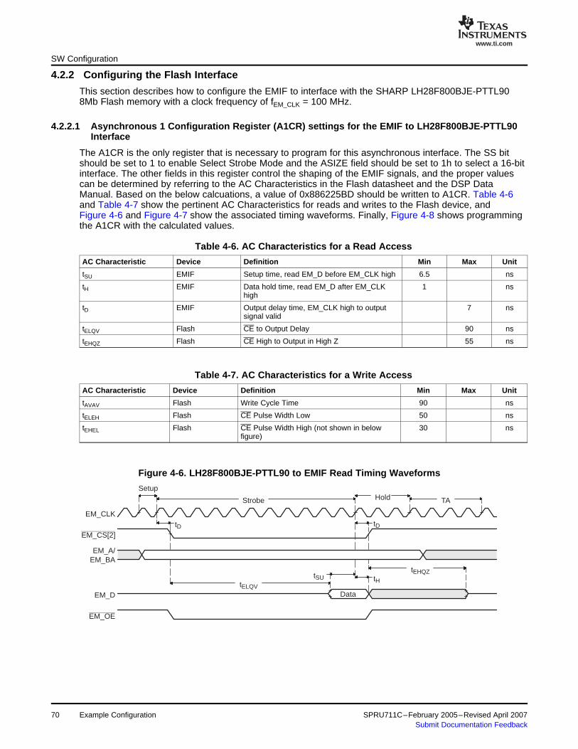
www.ti.com
4.2.2 Configuring the Flash Interface
4.2.2.1 Asynchronous 1 Configuration Register (A1CR) settings for the EMIF to LH28F800BJE-PTTL90
Setup
Strobe Hold TA
tD tD
tELQVtH
tSUtEHQZ
Data
EM_CLK
EM_CS[2]
EM_A/EM_BA
EM_D
EM_OE
SW Configuration
This section describes how to configure the EMIF to interface with the SHARP LH28F800BJE-PTTL908Mb Flash memory with a clock frequency of fEM_CLK = 100 MHz.
Interface
The A1CR is the only register that is necessary to program for this asynchronous interface. The SS bitshould be set to 1 to enable Select Strobe Mode and the ASIZE field should be set to 1h to select a 16-bitinterface. The other fields in this register control the shaping of the EMIF signals, and the proper valuescan be determined by referring to the AC Characteristics in the Flash datasheet and the DSP DataManual. Based on the below calcuations, a value of 0x886225BD should be written to A1CR. Table 4-6and Table 4-7 show the pertinent AC Characteristics for reads and writes to the Flash device, andFigure 4-6 and Figure 4-7 show the associated timing waveforms. Finally, Figure 4-8 shows programmingthe A1CR with the calculated values.
Table 4-6. AC Characteristics for a Read Access
AC Characteristic Device Definition Min Max Unit
tSU EMIF Setup time, read EM_D before EM_CLK high 6.5 ns
tH EMIF Data hold time, read EM_D after EM_CLK 1 nshigh
tD EMIF Output delay time, EM_CLK high to output 7 nssignal valid
tELQV Flash CE to Output Delay 90 ns
tEHQZ Flash CE High to Output in High Z 55 ns
Table 4-7. AC Characteristics for a Write Access
AC Characteristic Device Definition Min Max Unit
tAVAV Flash Write Cycle Time 90 ns
tELEH Flash CE Pulse Width Low 50 ns
tEHEL Flash CE Pulse Width High (not shown in below 30 nsfigure)
Figure 4-6. LH28F800BJE-PTTL90 to EMIF Read Timing Waveforms
70 Example Configuration SPRU711C–February 2005–Revised April 2007Submit Documentation Feedback
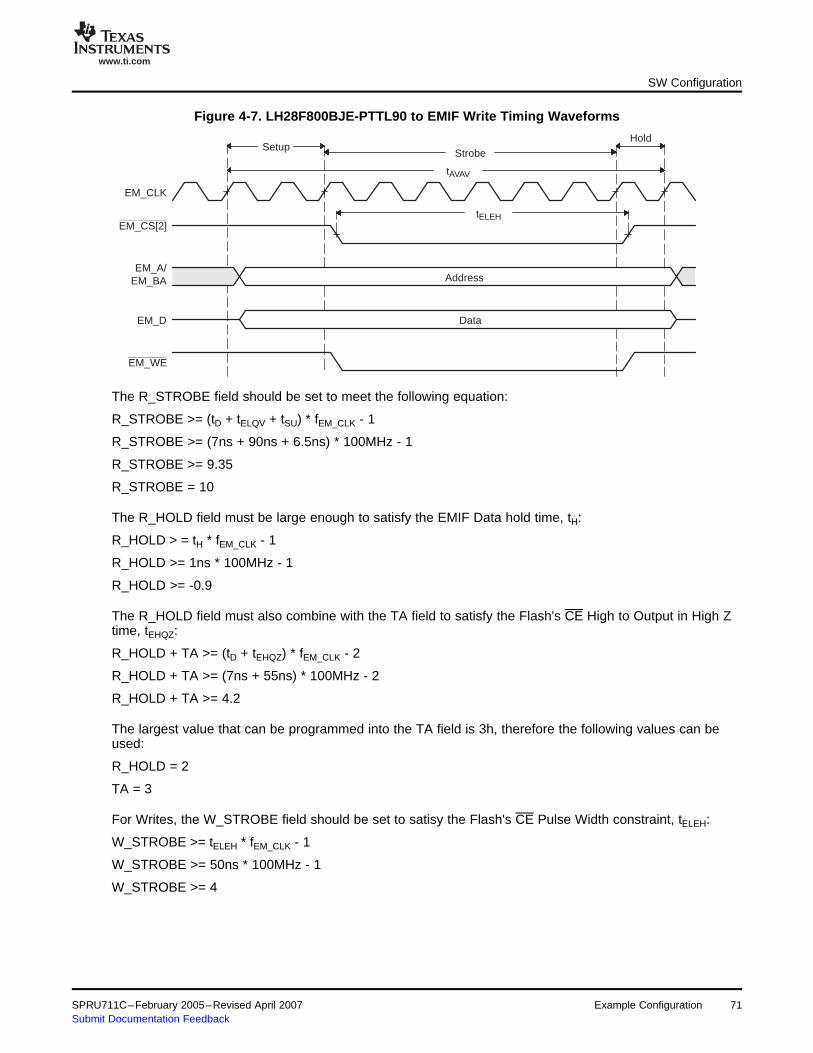
www.ti.com
SetupStrobe
Hold
tAVAV
tELEH
Data
Address
EM_CLK
EM_CS[2]
EM_A/EM_BA
EM_D
EM_WE
SW Configuration
Figure 4-7. LH28F800BJE-PTTL90 to EMIF Write Timing Waveforms
The R_STROBE field should be set to meet the following equation:
R_STROBE >= (tD + tELQV + tSU) * fEM_CLK - 1
R_STROBE >= (7ns + 90ns + 6.5ns) * 100MHz - 1
R_STROBE >= 9.35
R_STROBE = 10
The R_HOLD field must be large enough to satisfy the EMIF Data hold time, tH:
R_HOLD > = tH * fEM_CLK - 1
R_HOLD >= 1ns * 100MHz - 1
R_HOLD >= -0.9
The R_HOLD field must also combine with the TA field to satisfy the Flash's CE High to Output in High Ztime, tEHQZ:
R_HOLD + TA >= (tD + tEHQZ) * fEM_CLK - 2
R_HOLD + TA >= (7ns + 55ns) * 100MHz - 2
R_HOLD + TA >= 4.2
The largest value that can be programmed into the TA field is 3h, therefore the following values can beused:
R_HOLD = 2
TA = 3
For Writes, the W_STROBE field should be set to satisy the Flash's CE Pulse Width constraint, tELEH:
W_STROBE >= tELEH * fEM_CLK - 1
W_STROBE >= 50ns * 100MHz - 1
W_STROBE >= 4
SPRU711C–February 2005–Revised April 2007 Example Configuration 71Submit Documentation Feedback

www.ti.com
SW Configuration
The W_SETUP and W_HOLD fields should combine to satisfy the Flash's CE Pulse Width High constraint,tEHEL, when performing back-to-back writes:
W_SETUP + W_HOLD > = tEHEL * fEM_CLK - 2
W_SETUP + W_HOLD > = 30ns * 100MHz - 2
W_SETUP + W_HOLD > = 1
In addition, the entire Write access length must satisfy the Flash's minimum Write Cycle Time, tAVAV:
W_SETUP + W_STROBE + W_HOLD >= tAVAV * fEM_CLK - 3
W_SETUP + W_STROBE + W_HOLD >= 90ns * 100MHz - 3
W_SETUP + W_STROBE + W_HOLD >= 6
Solving the above equations for the Write fields results in the following possible solution:
W_SETUP = 1
W_STROBE = 5
W_HOLD = 0
Adding a 10ns (1 cycle) margin to each of the periods (excluding TA which is already at its maximum) inthis example produces the following recommended values:
W_SETUP = 2h
W_STROBE = 6h
W_HOLD = 1h
R_SETUP = 1h
R_STROBE = Bh
R_HOLD = 3h
TA = 3h
Figure 4-8. Asynchronous 1 Configuration Register (A1CR) [Offset 10h]
31 30 29 26 25 24
1 0 0010 00
SS EW W_SETUP W_STROBE
23 20 19 17 16
0110 001 0
W_STROBE W_HOLD R_SETUP
15 13 12 7 6 4 3 2 1 0
001 001011 011 11 01
R_SETUP R_STROBE R_HOLD TA ASIZE
LEGEND: R/W = Read/Write; R = Read only; -n = value after reset
Example Configuration72 SPRU711C–February 2005–Revised April 2007Submit Documentation Feedback

Appendix ASPRU711C–February 2005–Revised April 2007
Appendix A: Revision History
Changes made in this revision are shown in Table A-1.
Table A-1. Changes in This Revision
Location Changes, Additions, Deletions
Table 2-3 Updated text to EM_Wait pin description
Table 2-14 Modified pin ranges
Table 2-17 Modified description for EW parameter
Table 2-18 Added WRMSET parameter and description to Table 2-19
Table 2-20 Added WRMCLR parameter and description to Table 2-20
Section 2.5.6 Added Section, 2.5.6 NAND Flash Mode
Table 2-25 Added Table 2.25 Description of the NAND Flash Control Register (NANDFCR)
Section 2.5.6.1 Added Section 2.5.6.1 Configuring for NAND Flash Mode
Section 2.5.6.2 Added Section 2.5.6.2 Connecting to NAND Flash
Figure 2-15 Added Figure 2-14, EMIF to NAND Flash Interface
Section 2.5.6.3 Added Section 2.5.6.3, Driving CLE and ALE
Section 2.5.6.4 Added Section 2.5.6.4, NAND Read and Program Operations
Section 2.5.6.5 Added Section 2.5.6.5, NAND Data Read and Write via dMAX
Section 2.5.6.6 Added Section Section 2.5.6.6, ECC Generation
Figure 2-16 Added Figure 2.15, ECC Value for 8-Bit NAND Flash
Section 2.5.6.7 Added section NAND Flash Status Register (NANDFSR)
Section 2.5.6.8 Added Section 2.5.6.6, Interfacing to a Non-CE Don't Care NAND Flash
Section 2.8.1 Modified text to Section 2.8.1, Interrupt Events
Table 2-26 Modified Table 2-26, Interrupt Monitor and Control Bit Fields
Table 3-1 Added NANDFCR, NANDFSR, AND NANDF1ECC registers and description
Table 3-3 Changed bit 13 value to 0
Figure 3-4 Added (A) note to EW field in Figure 3-4
Table 3-8 Modified Table 3-8, EMIF Interrupt RAW Register Field Descriptions
Table 3-9 Modified Table 3-9, EMIF Interrupt Mask Register Field Descriptions
Figure 3-8 and Modified Figure 3-9 and Table 3-10, EMIF Interrupt Mask Set Register Field DescriptionsTable 3-10
Figure 3-10 and Modified Figure 3-10 and table 3-11, EMIF Interrupt Mask Clear Register Field DescriptionsTable 3-11
Figure 3-11 and Added Figure 3-11 and Table 3-12, NAND Flash Control Register Field DescriptionsTable 3-12
Figure 3-12 and Added Figure 3-12 and Table 3-13, NAND Flash Status Register Field DescriptionsTable 3-13
Figure 3-13 and Added Figure 3-13 and Table 3-14, NAND Flash 1 ECC Register Field DescriptionsTable 3-14
Section 4.2.1.5 Value of 0x00004520 chanbed to 0x00004720
SPRU711C–February 2005–Revised April 2007 Appendix A: Revision History 73Submit Documentation Feedback

www.ti.com
Appendix A
74 Appendix A: Revision History SPRU711C–February 2005–Revised April 2007Submit Documentation Feedback

IMPORTANT NOTICE
Texas Instruments Incorporated and its subsidiaries (TI) reserve the right to make corrections, modifications, enhancements,improvements, and other changes to its products and services at any time and to discontinue any product or service without notice.Customers should obtain the latest relevant information before placing orders and should verify that such information is current andcomplete. All products are sold subject to TI’s terms and conditions of sale supplied at the time of order acknowledgment.
TI warrants performance of its hardware products to the specifications applicable at the time of sale in accordance with TI’sstandard warranty. Testing and other quality control techniques are used to the extent TI deems necessary to support thiswarranty. Except where mandated by government requirements, testing of all parameters of each product is not necessarilyperformed.
TI assumes no liability for applications assistance or customer product design. Customers are responsible for their products andapplications using TI components. To minimize the risks associated with customer products and applications, customers shouldprovide adequate design and operating safeguards.
TI does not warrant or represent that any license, either express or implied, is granted under any TI patent right, copyright, maskwork right, or other TI intellectual property right relating to any combination, machine, or process in which TI products or servicesare used. Information published by TI regarding third-party products or services does not constitute a license from TI to use suchproducts or services or a warranty or endorsement thereof. Use of such information may require a license from a third party underthe patents or other intellectual property of the third party, or a license from TI under the patents or other intellectual property of TI.
Reproduction of information in TI data books or data sheets is permissible only if reproduction is without alteration and isaccompanied by all associated warranties, conditions, limitations, and notices. Reproduction of this information with alteration is anunfair and deceptive business practice. TI is not responsible or liable for such altered documentation.
Resale of TI products or services with statements different from or beyond the parameters stated by TI for that product or servicevoids all express and any implied warranties for the associated TI product or service and is an unfair and deceptive businesspractice. TI is not responsible or liable for any such statements.
TI products are not authorized for use in safety-critical applications (such as life support) where a failure of the TI product wouldreasonably be expected to cause severe personal injury or death, unless officers of the parties have executed an agreementspecifically governing such use. Buyers represent that they have all necessary expertise in the safety and regulatory ramificationsof their applications, and acknowledge and agree that they are solely responsible for all legal, regulatory and safety-relatedrequirements concerning their products and any use of TI products in such safety-critical applications, notwithstanding anyapplications-related information or support that may be provided by TI. Further, Buyers must fully indemnify TI and itsrepresentatives against any damages arising out of the use of TI products in such safety-critical applications.
TI products are neither designed nor intended for use in military/aerospace applications or environments unless the TI products arespecifically designated by TI as military-grade or "enhanced plastic." Only products designated by TI as military-grade meet militaryspecifications. Buyers acknowledge and agree that any such use of TI products which TI has not designated as military-grade issolely at the Buyer's risk, and that they are solely responsible for compliance with all legal and regulatory requirements inconnection with such use.
TI products are neither designed nor intended for use in automotive applications or environments unless the specific TI productsare designated by TI as compliant with ISO/TS 16949 requirements. Buyers acknowledge and agree that, if they use anynon-designated products in automotive applications, TI will not be responsible for any failure to meet such requirements.
Following are URLs where you can obtain information on other Texas Instruments products and application solutions:
Products Applications
Amplifiers amplifier.ti.com Audio www.ti.com/audio
Data Converters dataconverter.ti.com Automotive www.ti.com/automotive
DSP dsp.ti.com Broadband www.ti.com/broadband
Interface interface.ti.com Digital Control www.ti.com/digitalcontrol
Logic logic.ti.com Military www.ti.com/military
Power Mgmt power.ti.com Optical Networking www.ti.com/opticalnetwork
Microcontrollers microcontroller.ti.com Security www.ti.com/security
Low Power www.ti.com/lpw Telephony www.ti.com/telephonyWireless
Video & Imaging www.ti.com/video
Wireless www.ti.com/wireless
Mailing Address: Texas Instruments, Post Office Box 655303, Dallas, Texas 75265Copyright © 2007, Texas Instruments Incorporated