TMS320C6000 EMIF to External FIFO Interface - TI Report SPRA543 TMS320C6000 EMIF to External FIFO...
44
Application Report SPRA543 Digital Signal Processing Solutions May 1999 TMS320C6000 EMIF to External FIFO Interface Kyle Castille Digital Signal Processing Solutions Abstract Interfacing high-speed external first-in first-out (FIFO) memories to the Texas Instruments (TI™) TMS320C6000 digital signal processor (DSP) is possible via the ‘C6000’s external memory interface (EMIF). The EMIF is designed for a flexible interface to a wide variety of external memory devices. This document describes: FIFO types and characteristics EMIF control registers and asynchronous interface signals General example for each type of FIFO Full example for TI’s SN74ALVC7806 strobed FIFO Contents FIFO Interface ..................................................................................................................................................3 FIFO Types ...............................................................................................................................................5 Asynchronous/Strobed FIFO.....................................................................................................................6 Standard and FWFT Synchronous FIFOs...............................................................................................11 Special Considerations for Synchronous FIFOs .....................................................................................20 TI FIFO Selection Guide .........................................................................................................................20 Flag Polling .............................................................................................................................................21 Overview of EMIF...........................................................................................................................................22 EMIF Signal Descriptions........................................................................................................................22 EMIF Registers .......................................................................................................................................26 Full Example for Read Interface.....................................................................................................................27 Hardware Interface .................................................................................................................................28 Software Setup .......................................................................................................................................29 Full Example for Write Interface .....................................................................................................................35 Hardware Interface .................................................................................................................................36 Software Setup .......................................................................................................................................37 References.....................................................................................................................................................42
Transcript of TMS320C6000 EMIF to External FIFO Interface - TI Report SPRA543 TMS320C6000 EMIF to External FIFO...
Application ReportSPRA543
Digital Signal Processing Solutions May 1999
TMS320C6000 EMIF to External FIFOInterface
Kyle Castille Digital Signal Processing Solutions
Abstract Interfacing high-speed external first-in first-out (FIFO) memories to the Texas Instruments (TI™)TMS320C6000 digital signal processor (DSP) is possible via the ‘C6000’s external memoryinterface (EMIF). The EMIF is designed for a flexible interface to a wide variety of externalmemory devices.
This document describes:
r FIFO types and characteristics
r EMIF control registers and asynchronous interface signals
r General example for each type of FIFO
r Full example for TI’s SN74ALVC7806 strobed FIFO
Contents
FIFO Interface..................................................................................................................................................3FIFO Types ...............................................................................................................................................5Asynchronous/Strobed FIFO.....................................................................................................................6Standard and FWFT Synchronous FIFOs...............................................................................................11Special Considerations for Synchronous FIFOs .....................................................................................20TI FIFO Selection Guide .........................................................................................................................20Flag Polling .............................................................................................................................................21
Overview of EMIF...........................................................................................................................................22EMIF Signal Descriptions........................................................................................................................22EMIF Registers .......................................................................................................................................26
Full Example for Read Interface.....................................................................................................................27Hardware Interface .................................................................................................................................28Software Setup .......................................................................................................................................29
Full Example for Write Interface.....................................................................................................................35Hardware Interface .................................................................................................................................36Software Setup .......................................................................................................................................37
References.....................................................................................................................................................42
Application ReportSPRA543
TMS320C6000 EMIF to External FIFO Interface 2
FiguresFigure 1. Asynchronous FIFO Interface for Read Transmission ...................................................................7Figure 2. Asynchronous FIFO Read..............................................................................................................7Figure 3. Asynchronous FIFO Interface for Write Transmission ...................................................................8Figure 4. Asynchronous FIFO Write..............................................................................................................8Figure 5. Strobed FIFO Interface for Read Transmission .............................................................................9Figure 6. Strobed FIFO Read......................................................................................................................10Figure 7. Strobed FIFO Interface for Write Transmission............................................................................11Figure 8. FWFT Sync FIFO Interface for Write Transmission ......................................................................13Figure 9. FWFT FIFO Write Timing.............................................................................................................13Figure 10. FWFT Sync FIFO Interface for Read Transmission .....................................................................14Figure 11. FWFT FIFO Read ........................................................................................................................15Figure 12. Flag Timing for Last Read............................................................................................................16Figure 13. Synchronous FIFO Write Interface...............................................................................................17Figure 14. Synch FIFO Read Interface .........................................................................................................18Figure 15. Standard Synchronous FIFO Read..............................................................................................18Figure 16. ‘C6201/’C6701 EMIF SBSRAM Interface Block Diagram.............................................................22Figure 17. ‘C6202 EMIF SBSRAM Interface Block Diagram.........................................................................23Figure 18. ‘C6211/’C6711 EMIF SBSRAM Interface Block Diagram.............................................................24Figure 19. Byte Lane Alignment vs. Endianness on the ‘C6211/’C6711 .......................................................25Figure 20. ‘C6201/’C6202/’C6701 EMIF CE(0/1/2/3) Space Control Register Diagram................................26Figure 21. ‘C6211/’C6711 EMIF CE(0/1/2/3) Space Control Register Diagram ............................................26Figure 22. Read Interface for SN74ALVC7806 .............................................................................................28Figure 23. EMIF CE0 Space Control Register Diagram for ‘7806 .................................................................31Figure 24. Write Interface for SN74ALVC7806 .............................................................................................36Figure 25. EMIF CE0 Space Control Register Diagram for ‘7806 .................................................................38
TablesTable 1. EMIF—Input Timing Requirement Definitions .................................................................................3Table 2. EMIF—Output Timing Characteristics (Data, Address, Control) .....................................................3Table 3. EMIF—Other Timing Descriptions...................................................................................................4Table 4. FIFO—Input Timing Requirement ...................................................................................................4Table 5. FIFO—Output Timing Characteristics .............................................................................................4Table 6. External Logic—Output Timing Characteristics...............................................................................4Table 7. TI Low-Voltage FIFOs ...................................................................................................................20Table 8. Signals Used in FIFO Interface: Shared Signals and Asynchronous Signals................................24Table 9. EMIF Memory-Mapped Registers .................................................................................................26Table 10. EMIF CE(0/1/2/3) Space Control Registers Bitfield Description ....................................................27Table 11. EMIF Input Timing Requirement Definitions..................................................................................29Table 12. EMIF—Output Timing Characteristics (Data, Address, Control) ...................................................29Table 13. FIFO—Input Timing Requirement .................................................................................................29Table 14. FIFO—Output Timing Characteristics ...........................................................................................29Table 15. External Logic Characteristics of SN74LVC32A............................................................................29Table 16. EMIF—Output Timing Characteristics (Data, Address, Control) ...................................................37Table 17. FIFO—Input Timing Requirement .................................................................................................37Table 18. External Logic Characteristics of SN74LVC32A............................................................................37

Application ReportSPRA543
TMS320C6000 EMIF to External FIFO Interface 3
FIFO InterfaceThe asynchronous interface of the EMIF, which is used with FIFO memories, offers usersconfigurable memory cycle types used to interface to a variety of memory and peripheraltypes; including SRAM, EPROM, FLASH, as well as FPGA and ASIC designs. Thisdocument focuses on the interface between the EMIF and FIFO Memory.
In most situations when interfacing the ‘C6000 with an external FIFO, the FIFO is used inone direction only. That is, the ‘C6000 either writes to the FIFO, expecting some otherdevice (which could be another ‘C6000) to read from the FIFO, or reads from the FIFO,expecting some other device to write to the FIFO. Therefore, for all of the examplesgiven below, the diagrams are illustrated separately for the read interface and for thewrite interface to a given FIFO.
The EMIF does not have a glueless FIFO interface but instead uses a minimal amount ofglue logic to tie the asynchronous interface of the EMIF to external FIFOs. The followingdiscussion assumes an understanding of the asynchronous read/write cycles and theprogrammable parameters of these cycles.1
There are four basic types of FIFO memory, which are summarized in the followingsections.2 The timing notations used in all of the examples are summarized in Table 1through Table 6. In the following examples, the control signals going to the FIFOs areused in conjunction with the /CE signal. This is done to prevent any undesired behaviorfrom occurring if some other CE space also used asynchronous memory and thus alsoused the asynchronous interface pins. By ORing the asynchronous signals from theEMIF with the CE signal corresponding to the CE space where the FIFO resides, theFIFO is accessed only at the desired times. In some situations it is possible to eliminatesome or all of the glue, depending on the system environment.
The setup, strobe, and hold fields for both read and write cycles are fully programmablevia the EMIF CE space control registers. These fields must be set appropriately toensure proper operation with the FIFOs in the examples provided in the followingsections. The general constraints used to set these parameters are explained in thefollowing sections.
Table 1. EMIF—Input Timing Requirement Definitions
TimingParameter
Definition
tsu Data setup time, read D before CLKOUT1 high
th Data hold time, read D after CLKOUT1 high
Table 2. EMIF—Output Timing Characteristics (Data, Address, Control)
TimingParameter
Definition
td Output delay time, CLKOUT1 high to output signal valid
1 For details on the asynchronous memory cycles, see the TMS320C6201/6701 Peripherals
Reference Guide.
2 These summaries are not complete and are only intended to point out the major differencesbetween FIFO types. For complete details, see an appropriate data sheet.
Application ReportSPRA543
TMS320C6000 EMIF to External FIFO Interface 4
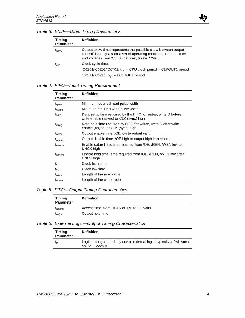
Table 3. EMIF—Other Timing Descriptions
TimingParameter
Definition
tskew Output skew time, represents the possible skew between outputcontrol/data signals for a set of operating conditions (temperatureand voltage). For ‘C6000 devices, tskew £ 2ns.
tcyc Clock cycle time.
‘C6201/’C6202/’C6701, tcyc = CPU clock period = CLKOUT1 period
‘C6211/’C6711, tcyc = ECLKOUT period
Table 4. FIFO—Input Timing Requirement
TimingParameter
Definition
trp(m) Minimum required read pulse width
twp(m) Minimum required write pulse width
tsu(m) Data setup time required by the FIFO for writes, write D beforewrite enable (async) or CLK (sync) high
tih(m) Data hold time required by FIFO for writes, write D after writeenable (async) or CLK (sync) high
toe(m) Output enable time, /OE low to output valid
toez(m) Output disable time, /OE high to output high impedance
tens(m) Enable setup time, time required from /OE, /REN, /WEN low toUNCK high
tenh(m) Enable hold time, time required from /OE, /REN, /WEN low afterUNCK high
tckh Clock high time
tckl Clock low time
trc(m) Length of the read cycle
twc(m) Length of the write cycle
Table 5. FIFO—Output Timing Characteristics
TimingParameter
Definition
tacc(m) Access time, from RCLK or /RE to ED valid
toh(m) Output hold time
Table 6. External Logic—Output Timing Characteristics
TimingParameter
Definition
tpl Logic propagation, delay due to external logic, typically a PAL suchas PALLV22V10.
Application ReportSPRA543
TMS320C6000 EMIF to External FIFO Interface 5
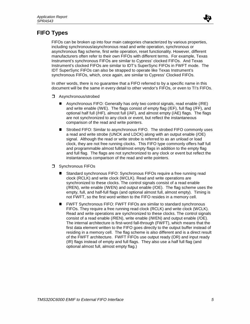
FIFO Types
FIFOs can be broken up into four main categories characterized by various properties,including synchronous/asynchronous read and write operation, synchronous orasynchronous flag scheme, first write operation, reset functionality. However, differentmanufacturers often refer to their own FIFOs with different terms. For example, TexasInstrument’s synchronous FIFOs are similar to Cypress’ clocked FIFOs. And TexasInstrument’s clocked FIFOs are similar to IDT’s SuperSync FIFOs in FWFT mode. TheIDT SuperSync FIFOs can also be strapped to operate like Texas Instrument’ssynchronous FIFOs, which, once again, are similar to Cypress’ Clocked FIFOs.
In other words, there is no guarantee that a FIFO referred to by a specific name in thisdocument will be the same in every detail to other vendor’s FIFOs, or even to TI’s FIFOs.
r Asynchronous/strobed
n Asynchronous FIFO: Generally has only two control signals, read enable (/RE)and write enable (/WE). The flags consist of empty flag (/EF), full flag (/FF), andoptional half full (/HF), almost full (/AF), and almost empty (/AE) flags. The flagsare not synchronized to any clock or event, but reflect the instantaneouscomparison of the read and write pointers.
n Strobed FIFO: Similar to asynchronous FIFO. The strobed FIFO commonly usesa read and write strobe (UNCK and LDCK) along with an output enable (/OE)signal. Although the read or write strobe is referred to as an unload or loadclock, they are not free running clocks. This FIFO type commonly offers half fulland programmable almost full/almost empty flags in addition to the empty flagand full flag. The flags are not synchronized to any clock or event but reflect theinstantaneous comparison of the read and write pointers.
r Synchronous FIFOs
n Standard synchronous FIFO: Synchronous FIFOs require a free running readclock (RCLK) and write clock (WCLK). Read and write operations aresynchronized to these clocks. The control signals consist of a read enable(/REN), write enable (/WEN) and output enable (/OE). The flag scheme uses theempty, full, and half-full flags (and optional almost full, almost empty). Timing isnot FWFT, so the first word written to the FIFO resides in a memory cell.
n FWFT Synchronous FIFO: FWFT FIFOs are similar to standard synchronousFIFOs. They require a free running read clock (RCLK) and write clock (WCLK).Read and write operations are synchronized to these clocks. The control signalsconsist of a read enable (/REN), write enable (/WEN) and output enable (/OE).The internal architecture is first-word fall-through (FWFT), which means that thefirst data element written to the FIFO goes directly to the output buffer instead ofresiding in a memory cell. The flag scheme is also different and is a direct resultof the FWFT architecture. FWFT FIFOs use output ready (OR) and input ready(IR) flags instead of empty and full flags. They also use a half full flag (andoptional almost full, almost empty flag.)

Application ReportSPRA543
TMS320C6000 EMIF to External FIFO Interface 6
Asynchronous/Strobed FIFO
Because the asynchronous and strobed FIFOs are so similar, they are explainedtogether. The first data written to the FIFO falls through to the output buffer of the FIFOand is available for the next read, which is indicated by the /EF becoming invalid. Whena read is issued, the data in the output buffer is read, and the next data in the memoryarray (pointed to by the FIFO read pointer) is brought to the output buffer in preparationfor the next read. This maps perfectly to the asynchronous interface of the EMIFbecause data is latched by the ‘C6000 when the /ARE signal becomes inactive.
Asynchronous FIFO
For asynchronous FIFOs, data reads and writes are not edge-triggered. Instead, datawrites are initiated by a low level on write enable (/W) when the full flag is not asserted.The data is actually written on the rising edge of the write-enable signal. Data reads areinitiated by low level on read enable (/R) when the empty flag is not asserted. For thistype of FIFO, it is actually the /R signal that takes the output data bus (Q[x:0]) out of highimpedance state immediately before the data becomes valid, as shown in Figure 2.Figure 1 and Figure 3 show the interface between the EMIF and two 18-bit-wideasynchronous FIFOs. The EMIF directly interfaces to the lower 16 bits of each FIFO,logically combining them to appear as a single 32-bit-wide FIFO. This is referred to aswidth expansion and is covered in detail in most FIFO data sheets.
The external logic block shown in Figure 1 and Figure 3 is required to glue the EMIF tothe FIFO. Of primary concern in this example is that the /R and /W signal on the FIFO isonly activated when this memory space is activated (by the /CE signal). This can bedone by ORing the appropriate strobe signal with the /CE signal:
r /R = /CE + /ARE
r /W = /CE + /AWE
Figure 2 shows the timing diagram illustrating both the outputs from the EMIF and theinputs to the asynchronous FIFO for a read cycle. Figure 6 shows the write cycle.

Application ReportSPRA543
TMS320C6000 EMIF to External FIFO Interface 7
Figure 1. Asynchronous FIFO Interface for Read Transmission
Logic
External MemoryInterface (EMIF)
/ARE
/CEn
/AOE
/AWE
ED[31:16]
ED[15:0]
AsynchronousFIFO
/R / W
/EF
Q[17:0] D[17:0]
/HF
/FF
INTxINTy
AsynchronousFIFO
/R / W
/EF
Q[17:0] D[17:0]
/HF
/FF
INTz
Figure 2. Asynchronous FIFO Read
Setup Strobe Hold Setup Strobe Hold
D1 D2
C6x latches dataC6x latches data
trc(m)trp(m)
tpl
tsutacc(m)
td
td
Clock *
/CE
/ARE
ED [31:0]
/R = /CE + /ARE
Timing Constraints for Asynchronous FIFO Read Interface
r Setup ³ 1 (minimum allowed by ‘C6000)
r Strobe ³ (tdmax + tplmax + tacc(m) + tsu)/tcyc
r Strobe ³ (trp(m))/tcyc
r Strobe + Hold + Setup ³ (trc(m))/tcyc

Application ReportSPRA543
TMS320C6000 EMIF to External FIFO Interface 8
Figure 3. Asynchronous FIFO Interface for Write Transmission
Logic
External MemoryInterface (EMIF)
/ARE
/CEn
/AOE
/AWE
ED[31:16]
ED[15:0]
AsynchronousFIFO
/ W /R
/EF
D[17:0] Q[17:0]
/HF
/FF
INTxINTy
AsynchronousFIFO
/ W /R
/EF
D[17:0] Q[17:0]
/HF
/FF
INTz
Figure 4. Asynchronous FIFO Write
Setup Strobe Hold Setup Strobe Hold
D1 D2
FIFO sampFIFO samples data
tpltwp(m)
tpltwc(m)
tih(mtdtsu(m)
td
Clock *
/CE
/AWE
ED [31:0]
/W = /CE + /AWE
Timing Constraints for Asynchronous FIFO Write Interface
r Setup ³ 1 (minimum allowed by ‘C6000)
r Strobe ³ (twp(m))/tcyc
r Setup + Strobe ³ (tsu(m)+ tskew – tplmin)/tcyc
r Setup + Strobe + Hold ³ (twc(m))/tcyc
r Hold ³ (tskew + tplmax + tih(m))/tcyc

Application ReportSPRA543
TMS320C6000 EMIF to External FIFO Interface 9
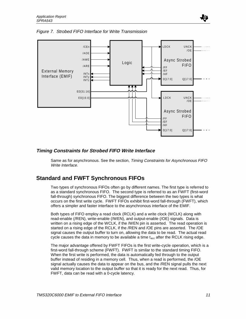
Async Strobed FIFO
The strobed FIFO is similar to the asynchronous FIFO. The addition of an output-enable(/OE) signal, which is responsible for 3-stating the output data bus, allows the FIFO touse the read-enable signal (UNCK) as an edge trigger. The write cycle is identical to theasynchronous FIFO write cycle.
Figure 5 and Figure 7 show the interface between the EMIF and two 18-bit-wide strobedFIFOs. The EMIF directly interfaces to the lower 16 bits of each FIFO, logicallycombining them to appear as a single 32-bit-wide FIFO. This is referred to as widthexpansion and is covered in detail in most FIFO data sheets.
The external logic block shown in Figure 5 and Figure 7 is required to glue the EMIF tothe FIFO. The UNCK, LDCK, and /OE signals can be created by logically ORing theasynchronous control signals from the EMIF as follows:
r UNCK = /CE + /ARE
r LDCK = /CE + /AWE
r /OE = /CE + /AOE
Figure 5 shows the timing diagram illustrating both the outputs from the EMIF and theinputs to the strobed FIFO for a read cycle. The write cycle is not shown because it isidentical to the cycle shown above for asynchronous FIFO. These timing diagramsillustrate the creation of the FIFO signals with the above logic.
Figure 5. Strobed FIFO Interface for Read Transmission
Logic
External MemoryInterface (EMIF)
/ARE
/CEn
/AOE
/AWE
ED[31:16]
ED[15:0]
Async StrobedFIFO
U N C K L D C K
/EF
Q[17:0] D[17:0]
/HF
/FF
/OE
INTxINTy
Async StrobedFIFO
L D C K
/EF
Q[17:0] D[17:0]
/HF
/FF
INTz
U N C K/OE
Application ReportSPRA543
TMS320C6000 EMIF to External FIFO Interface 10
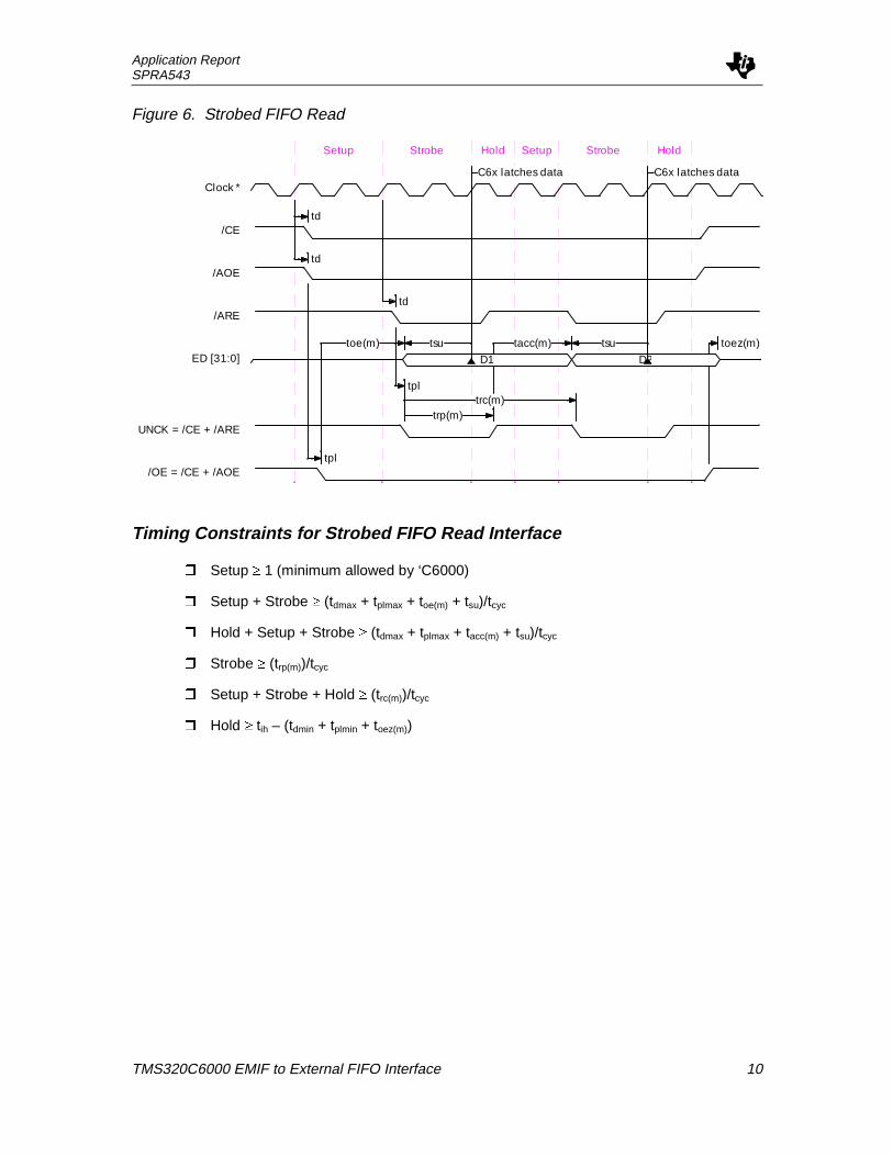
Figure 6. Strobed FIFO Read
Setup Strobe Hold Setup Strobe Hold
D1 D2
C6x latches dataC6x latches data
tpl
trc(m)trp(m)
tpl
toez(m)tsutacc(m)tsutoe(m)
td
td
td
Clock *
/CE
/AOE
/ARE
ED [31:0]
UNCK = /CE + /ARE
/OE = /CE + /AOE
Timing Constraints for Strobed FIFO Read Interface
r Setup ³ 1 (minimum allowed by ‘C6000)
r Setup + Strobe ³ (tdmax + tplmax + toe(m) + tsu)/tcyc
r Hold + Setup + Strobe ³ (tdmax + tplmax + tacc(m) + tsu)/tcyc
r Strobe ³ (trp(m))/tcyc
r Setup + Strobe + Hold ³ (trc(m))/tcyc
r Hold ³ tih – (tdmin + tplmin + toez(m))
Application ReportSPRA543
TMS320C6000 EMIF to External FIFO Interface 11
Figure 7. Strobed FIFO Interface for Write Transmission
Logic
External MemoryInterface (EMIF)
/ARE
/CEn
/AOE
/ A W E
ED[31:16]
ED[15:0]
Async StrobedFIFO
L D C K U N C K
/EF
D[17:0] Q[17:0]
/HF
/FF
/OE
INTxINTy
Async StrobedFIFO
U N C K
/EF
D[17:0] Q[17:0]
/HF
/FF
INTz
L D C K/OE
Timing Constraints for Strobed FIFO Write Interface
Same as for asynchronous. See the section, Timing Constraints for Asynchronous FIFOWrite Interface.
Standard and FWFT Synchronous FIFOs
Two types of synchronous FIFOs often go by different names. The first type is referred toas a standard synchronous FIFO. The second type is referred to as an FWFT (first-wordfall-through) synchronous FIFO. The biggest difference between the two types is whatoccurs on the first write cycle. FWFT FIFOs exhibit first-word fall-through (FWFT), whichoffers a simpler and faster interface to the asynchronous interface of the EMIF.
Both types of FIFO employ a read clock (RCLK) and a write clock (WCLK) along withread-enable (/REN), write-enable (/WEN), and output-enable (/OE) signals. Data iswritten on a rising edge of the WCLK, if the /WEN pin is asserted. The read operation isstarted on a rising edge of the RCLK, if the /REN and /OE pins are asserted. The /OEsignal causes the output buffer to turn on, allowing the data to be read. The actual readcycle causes the data in memory to be available a time tacc after the RCLK rising edge.
The major advantage offered by FWFT FIFOs is the first write-cycle operation, which is afirst-word fall-through scheme (FWFT). FWFT is similar to the standard timing FIFO.When the first write is performed, the data is automatically fed through to the outputbuffer instead of residing in a memory cell. Thus, when a read is performed, the /OEsignal actually causes the data to appear on the bus, and the /REN signal pulls the nextvalid memory location to the output buffer so that it is ready for the next read. Thus, forFWFT, data can be read with a 0-cycle latency.

Application ReportSPRA543
TMS320C6000 EMIF to External FIFO Interface 12
FWFT Synchronous FIFO Interface
The external logic block shown in Figure 10 and Figure 8 may be required to glue theEMIF to a FWFT sync FIFO. The /REN, /WEN, and /OE signals are created by logicallyORing the asynchronous control signals from the EMIF as follows:
r RCLK = /ARE
r WCLK = /AWE
r /WEN = /CEx + ! (/AOE)
r /REN = /CEx + /AOE
r /OE = /CEx + /AOE
Note that no glue is required to create the RCLK and WCLK signals of the FIFO. This isbecause synchronous FIFOs are designed to operate with a free running clock. By notgating RCLK and WCLK with the /CE signal, extra clock pulses may be seen by the FIFOwhen EMIF accesses to other CE spaces occur. This gives the advantage of updatingthe FIFO state while not accessing the FIFO, because the internal state of the FIFO isupdated on a read and/or write clock edge.
In addition, if only a single direction interface is used in a CE space, glue can be avoidedfor this interface. For example, if only a write FIFO is used in CE1, the /CE1 output canbe used directly as the /WEN signal of the FIFO. Similarly, if a read FIFO is used in CE2,the /CE2 output can be used directly as the /REN signal of the FIFO. When operatingwith a no-glue interface, it is possible to inadvertently access the FIFO by performingincorrect access. Based on the previous example, if a write to CE2 (which contains aread FIFO) is performed inadvertently, the /CE2 signal will be asserted externally and willturn on the output data buffers of the FIFO via the /OE input. At the same time, data willbe driven by the ‘C6000 EMIF, causing data contention on the bus and potential damageto both devices. Also, if a glueless interface as described here is implemented, careshould be taken to not access these memory spaces via a debugger memory window, asthis changes the state of the FIFO and possibly causes contention on the data bus.
FWFT Sync FIFO Write Interface
From the FIFO writer’s control signal point of view, there is no functional differencebetween FWFT and standard synchronous FIFOs since data is always written with a 0-cycle latency. That is, the FIFO latches data at the same time as the write command isreceived.
For FWFT FIFOs, because the output buffer is used as a valid storage location (the firstwrite goes directly to the output buffer), D + 1 writes can occur before the FIFO is full (theinput is no longer ready), where D is the depth of the FIFO. As a result of this, FWFTFIFOs use an input ready flag (IR) flag rather than a full flag (FF) to indicate the subtledifference. The input ready flag indicates whether the entire FIFO depth (D) plus theoutput buffer is occupied.

Application ReportSPRA543
TMS320C6000 EMIF to External FIFO Interface 13
Figure 8. FWFT Sync FIFO Interface for Write Transmission
Logic
External MemoryInterface (EMIF)
/ARE
/CEn
/AOE
/AWE
ED[31:16]
ED[15:0]
FWFT SyncFIFO
O R
D[17:0] Q[17:0]
/HF
IR
INTxINTy
FWFT SyncFIFO
O R
D[17:0] Q[17:0]
/HF
IR
INTz
W C L K/ W E N
R C L K/REN
/OE
W C L K/ W E N
R C L K/REN
/OE
Figure 9. FWFT FIFO Write Timing
Setup Strobe Hold Setup Strobe Hold
D1 D2
FIFO latchesFIFO latches data
tpltens(m)
tckh(m)twc(m)
tckl(m)
td
tih(m)tsu(m)tsu(m)
td
td
td
Clock *
/CE
/AWE
/AOE
ED [31:0]
WCLK = /AWE
/WEN = /CE + ! (/AOE)

Application ReportSPRA543
TMS320C6000 EMIF to External FIFO Interface 14
Timing Constraints for FWFT Write Interface
r Setup ³ 1
r Setup + Strobe ³ (tsu(m) + tskew) /tcyc
r Setup + Strobe ³ (tens(m) + tplmax + tskew)/tcyc
r Strobe ³ (tckl(m))/tcyc
r Hold + Setup ³ (tckh(m))/tcyc
r Setup + Strobe + Hold ³ (twc(m))/tcyc
r Hold ³ (tih(m) + tskew)/tcyc
FWFT Sync FIFO Read Interface
From the FIFO reader’s point of view, the FWFT FIFO offers a significant advantage overa standard synchronous FIFO because the asynchronous interface of the EMIF is used.Standard synchronous FIFOs are ideal for the situation where the memory controllerlatches the data one cycle after the read command is issued. The EMIF asynchronousinterface instead latches data at the end of the strobe period.
Figure 11 shows two back-to-back reads from a FWFT FIFO. Because the first datawritten to the FIFO automatically goes to the output buffer, the /OE signal of the FIFObrings valid data to the data bus and is latched by the ‘C6000. The rising edge of RCLKbrings the next data to the output buffer in preparation for the next read.
Figure 10. FWFT Sync FIFO Interface for Read Transmission
Logic
External MemoryInterface (EMIF)
/ARE
/CEn
/AOE
/AWE
ED[31:16]
ED[15:0]
FWFT SyncFIFO
R C L K W C L K
O R
Q[17:0] D[17:0]
/HF
IR
/REN
INTxINTy
FWFT SyncFIFO
O R
Q[17:0] D[17:0]
/HF
IR
INTz
/OE/ W E N
R C L K/REN/OE
W C L K/ W E N

Application ReportSPRA543
TMS320C6000 EMIF to External FIFO Interface 15
Figure 11. FWFT FIFO Read
Setup Strobe Hold Setup Strobe Hold
D1 D2
Valid ReadValid Read
tpl
tckh(m)
trc(m)tckl(m)
tens(m)
td
toetih
tsutacc(m)tsutoe(m)
td
td
td
Clock *
/CE
/AOE
/ARE
ED [31:0]
RDCLK = /ARE
/RE=/OE=/CE+/AOE
OR
Timing Constraints for FWFT Read Interface
r Setup ³ 1
r Setup + Strobe ³ (tdmax + tplmax + toe(m) + tsu)/tcyc
r Setup + Strobe ³ (tens(m) + tplmax + tskew)/tcyc
r Strobe ³ (tckl(m))/tcyc
r Hold + Setup ³ (tckh(m))/tcyc
r Setup + Strobe + Hold ³ (trc(m))/tcyc
r Hold + Setup + Strobe ³ (tdmax + tacc(m) + tsu)/tcyc
FWFT Flag Scheme
Because the FWFT FIFO offers an additional valid storage location in the output buffer, aslightly different flag scheme is used. The FWFT FIFO uses an output ready flag (OR)rather than an empty flag (/EF) to indicate that valid data is in the output buffer.

Application ReportSPRA543
TMS320C6000 EMIF to External FIFO Interface 16
Figure 12 shows the scenario for the last read from a FWFT FIFO. Q(D) represents thesecond to last valid data and Q(D+1) shows the last piece of valid data. During the firstread, Q(D) is in the output buffer, and the read command brings Q(D+1) to the outputbuffer in preparation for the last read. As the diagram shows, the OR flag indicates thatunread data is in the output buffer and does not go low until after the last data is readfrom the output buffer.
Figure 12. Flag Timing for Last Read
Setup Strobe Hold Setup Strobe Hold
Q(D) Q(D+1 Q(D+1)
C6x latches dataC6x latches data
tacctoe
Clock *
/CE
/AOE
/ARE
ED [31:0]
RDCLK = /CE + /ARE
/RE = /OE = /CE + /AOE
OR
Standard Synchronous FIFO Interface
The external logic block shown in Figure 13 and Figure 14 is required to glue the EMIF toa standard synchronous FIFO. The /REN, /WEN, and /OE signals are created bylogically ORing the asynchronous control signals from the EMIF with the CE signal.
r RCLK = ! (/ARE)
r WCLK = /AWE
r /WEN = /CEx + ! (/AOE)
r /REN = /CEx + /AOE
r /OE = /CEx + /AOE
Notice that the logic required for the write interface is identical to that used for the FWFTsync FIFO write interface. The read interface is similar, except the RCLK signal must beinverted to allow the read data to be latched a time tacc(m) after the read command. Ifdesired, the interface used for the FWFT interface can be used for the standard interfaceas well, but software complexities arise because the first word read from an empty FIFOwould be invalid.

Application ReportSPRA543
TMS320C6000 EMIF to External FIFO Interface 17
Standard Sync FIFO Write Interface
For standard synchronous FIFOs, D (D = FIFO depth) writes can occur before the FIFOis full because the first write goes directly to a memory cell and the output buffer is notused as a valid storage location. This is the only difference between a standardsynchronous FIFO write interface and a FWFT FIFO write interface. The timing is thesame as defined above for the FWFT FIFO write interface.
Figure 13. Synchronous FIFO Write Interface
ExternalLogic
External MemoryInterface (EMIF)
/ARE
/CEn
/AOE
/AWE
ED[31:16]
ED[15:0]
SynchronousFIFO
/EF
D[17:0] Q[17:0]
/HF
/FF
INTxINTy
SynchronousFIFO
/EF
D[17:0] Q[17:0]
/HF
/FF
INTz
W C L K/ W E N
R C L K/REN
/OE
W C L K/ W E N
R C L K/REN
/OE
Standard Sync FIFO Read Interface
With a standard synchronous FIFO, the first data written to the FIFO after reset remainsin a memory cell and the output buffer is empty. For the first read access, the read isstarted when /REN is active at the rising edge of RCLK, and brings the data to the outputbuffer a time tacc after RCLK goes high.
Therefore, to interface to a standard synchronous FIFO, the output read strobe of the‘C6000 must be inverted so that the ‘C6000 latches data on the falling edge of the readstrobe. The drawback to this approach is that the programmed Read Strobe period of the‘C6000 must be extended to accommodate the access time of the FIFO. This is shown inFigure 15.

Application ReportSPRA543
TMS320C6000 EMIF to External FIFO Interface 18
Figure 14. Synch FIFO Read Interface
ExternalLogic
External MemoryInterface (EMIF)
/ARE
/CEn
/AOE
/AWE
ED[31:16]
ED[15:0]
SynchronousFIFO
R C L K W C L K
/EF
Q[17:0] D[17:0]
/HF
/FF
/REN
INTxINTy
SynchronousFIFO
/EF
Q[17:0] D[17:0]
/HF
/FF
INTz
/OE/ W E N
R C L K/REN/OE
W C L K/ W E N
Figure 15. Standard Synchronous FIFO Read
Setup Strobe Hold Setup Strobe Hold
D1 D2
Valid ReadC6x Latches Data
tpl
tckl(m)trc(m)
tckh(m)
tpl
tens(m)
tihtsu
tacc(m)tsu
tacc(m)toe(m)
td
td
td
Clock *
/CE
/AOE
/ARE
ED [31:0]
RDCLK = ! (/ARE)
/RE = /OE = /CE + /AOE
/EF
Application ReportSPRA543
TMS320C6000 EMIF to External FIFO Interface 19
Timing Constraints for Standard Sync FIFO Read Interface
r Setup ³ 1
r Strobe ³ (tdmax + tplmax + tacc(m) + tsu)/tcyc
r Setup ³ (tens(m) + tskew)/tcyc
r Strobe ³ (tckh(m))/tcyc
r Hold + Setup ³ (tckl(m))/tcyc
r Setup + Strobe + Hold ³ (trc(m))/tcyc
Sync FIFO Flag Synchronization
Another key feature of FWFT and standard synchronous FIFOs is that flags aresynchronized to either the read or write clock. The read clock controls /EF for standardsync FIFOs and OR for FWFT sync FIFOs. The write clock controls /FF for standardsynchronous FIFOs and IR for FWFT sync FIFOs. The boundary flags are only updatedby a rising edge of its controlling clock3. This presents a problem for both types of FIFOsbecause the EMIF is using an asynchronous interface and there is no free running clocktied to the FIFO.
For example, if the FIFO is empty, a write to the FIFO causes data to go to a location inthe FIFO. However, the OR/EF flag does not get updated until there is a pulse at theRCLK input. This can be accomplished in several ways.
r First, because the clock input of the FIFO in the above solutions are not gated by the/CEx signal, if accesses to other memory spaces cause the /ARE and/or /AWE signalto toggle, the appropriate flag of the FIFO will be updated.
r Another alternative is possible, if unused memory spaces are in the system. If this isthe case, the empty memory space can be defined as an asynchronous memorytype. If the FIFO flags are not up to date, reads or writes can be done to the emptymemory space, causing the FIFO clock to toggle and update its state. If desired, thiscan be set up as a periodic DMA transaction or a periodic interrupt software routineso that polling will not be necessary.
r A third alternative can be used, if the first two are not possible. If the FIFO flags arenot up to date, issuing a dummy access to the FIFO will force the state to update.For example, if the OR/EF flag indicates an empty state even though there is data inthe FIFO, a dummy read will not actually read data from the FIFO but merely updatethe OR flag, indicating that the next read will proceed as desired. Similarly, if a readis done from a full FIFO, a dummy write must be issued to get the IR/FF to update.
3 This usually does not apply to half-full and amost-full/almost empty flags but may for some
devices.

Application ReportSPRA543
TMS320C6000 EMIF to External FIFO Interface 20
Special Considerations for Synchronous FIFOs
The following list contains peculiarities associated with certain FIFOs. This list is far fromcomplete but is included to assist the user in making avoidable design errors. Therefore,the user should ensure that the chosen FIFO for a given design meets the timingrequirements of the ‘C6000 and that both the ‘C6000’s operation and the FIFO’soperation is fully understood.
r Some synchronous FIFOs have special reset requirements that require a givennumber of RCLK and WCLK cycles to occur while the reset signal is active low. Thisis a problem with the interface discussed because the solution provided uses the/ARE and /AWE to create a clock and thus does not have a free-running clockprovided to the FIFO. A ‘C6000 general-purpose output can be used as the resetsignal of the FIFO. The ‘C6000 can then force clock transitions before releasingreset.
r Some synchronous FIFOs offer a single AF/AE signal instead of two distinct AF andAE signals. To create a dedicated AF (or AE) input to the ‘C6000, external logic mustbe used to determine the state based on the status of the other state flags.
r Do not assume that a particular FIFO behaves exactly as this document describesbecause of the many variations that exist.
TI FIFO Selection Guide
Texas Instruments has six low-voltage FIFOs that fall into two categories: three strobedFIFOs and three FWFT synchronous FIFOs. These devices are summarized in Table 7.
Table 7. TI Low-Voltage FIFOs
EMIF Pin FIFO Signal Description
SN74ALVC7804 512 x 18, 40-MHz operation with toe = 10 ns and tacc = 18 ns
SN74ALVC7806 256 x 18, 40-MHz operation with toe = 10 ns and tacc = 18 ns
StrobedFIFO
SN74ALVC7814 64 x 18, 40-MHz operation with toe = 10 ns and tacc = 18 ns
SN74ALVC7803 512 x 18, 50-MHz operation with toe = 11 ns and tacc = 13 ns
SN74ALVC7805 256 x 18, 50-MHz operation with toe = 11 ns and tacc = 13 ns
FWFT SyncFIFO
SN74ALVC7813 64 x 18, 50-MHz operation with toe = 11 ns and tacc = 13 ns
These devices are well suited to interfacing to the EMIF of the ‘C6000 series of DSPs.The Full Example for Read Interface and Full Example for Write Interface sectionsprovide a complete description of the interface between a ‘C6000 DSP and a strobedFIFO.
The advantages and disadvantages associated with both types of interface aresummarized below:
Application ReportSPRA543
TMS320C6000 EMIF to External FIFO Interface 21
Strobed FIFO
r Advantages
n Simpler software interface because boundary flags (OR and IR) update withoutneeding a free running clock
r Disadvantages
n Requires glue, regardless of system configuration
n Slightly slower interface than TI’s FWFT Sync FIFOs
FWFT Sync FIFO
r Advantages
n Requires glue for generic interface. If only a single FIFO direction is used in aCE space, glue can be avoided.
n Slightly faster interface than TI’s strobed FIFOs
r Disadvantages
n More complicated software because boundary flags are only updated when aCLK edge is detected at the FIFO. This means dummy reads and/or writes mayneed to be issued to the FIFO to get the state to update.
Flag Polling
Several options can be used to control reading/writing to a FIFO efficiently. A couple ofdifferent options include software polling and hardware control via the DMA (directmemory access) and interrupts. The ‘C6000 can use all of the available flags to controlaccess to the FIFO or only a subset, depending on which factors are important.
Software polling is a simple and effective way to service a FIFO. Unused McBSP pins ortimer input pins can be used as general-purpose inputs. The FIFO flags can be input intothe appropriate general-purpose input and, depending on the state of the flags, access tothe FIFO can occur. For example, if high throughput is important, the full flag can bemonitored, and a DMA read burst equal to the depth of the FIFO can be performed whenthe FIFO is full. Or if the FIFO is half full but not full, a DMA read burst equal to half theFIFO depth can be performed.
If high throughput is not desired but low latency is important instead, the empty flag canbe monitored. Whenever the FIFO is not empty, reads can be done until it is empty.
Other means of control could use an external interrupt that could automatically trigger theDMA to perform a burst. For example, if the /FF were tied to an external interrupt, itcould trigger a DMA read burst equal to the depth of the FIFO.
There are several situations to be aware of:
r If the FIFO is allowed to become full, the write end of the FIFO will be blocked.
r If the FIFO becomes empty, the read end of the FIFO will be blocked.
r If just the HF flag is used to trigger bursts, it is possible to become ‘stuck’ in one halfof the FIFO; stuck half full, or stuck half empty, depending on the implementation of

Application ReportSPRA543
TMS320C6000 EMIF to External FIFO Interface 22
the HF flag. For example, if the HF represents half full or more and the FIFObecomes full, a read burst of D/2 does not take the FIFO out of the half-full state. Orif the half-full flag represents more than half full and the FIFO becomes empty, a writeburst of D/2 does not take the FIFO out of the less than half-full state.
The ideal solution allows maximum throughput, minimal software intervention, minimalamount of resources used (interrupts and general-purpose inputs), and minimal head-of-line blocking.
Overview of EMIF
EMIF Signal Descriptions
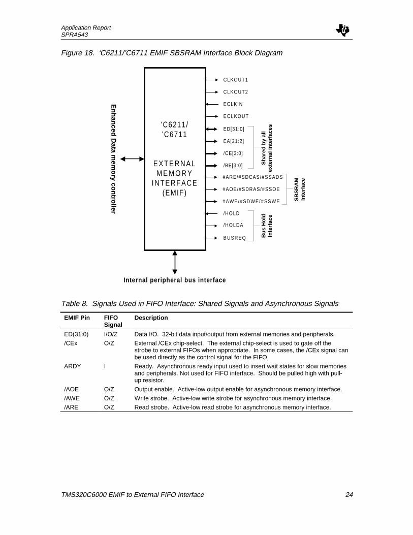
Figure 16 shows a block diagram of the EMIF, the interface between external memoryand the other internal units of the ‘C6000. The signals described in Table 8, however,focus on the asynchronous interface and the shared interface signals, which are used foran interface between the ‘C6000 and an external FIFO.
Figure 16. ‘C6201/’C6701 EMIF SBSRAM Interface Block Diagram
Sha
red
by a
llex
tern
al in
terf
aces
Internal peripheral bus interface
DM
A interface
Data A
ccessP
rogram A
ccess
ED[31:0]
EA[21:2]
/CE[3:0]
/BE[3:0]
'C6201/'C6701
E X T E R N A LM E M O R Y
INTERFACE(EMIF)
CLKOUT1
CLKOUT2
SB
SR
AM
Inte
rfac
eB
us H
old
Inte
rfac
e
/SSADS
/SSOE
/SSWE
SSCLK
/HOLD
/HOLDA
Application ReportSPRA543
TMS320C6000 EMIF to External FIFO Interface 23
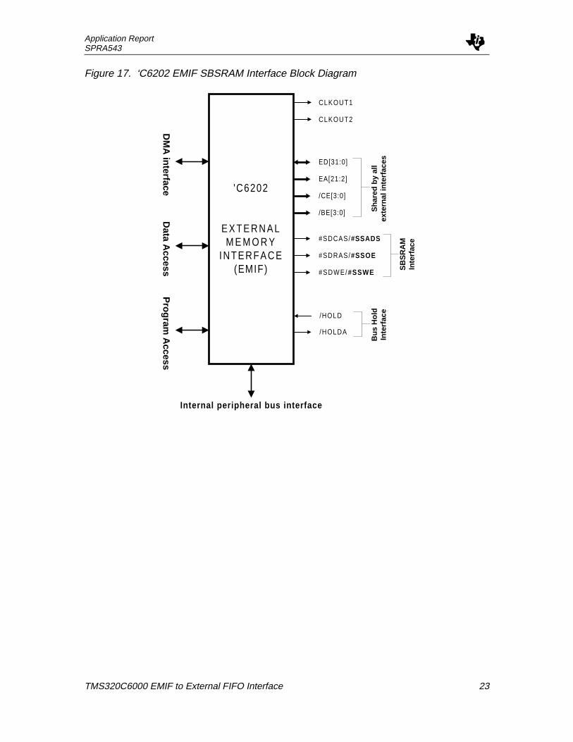
Figure 17. ‘C6202 EMIF SBSRAM Interface Block Diagram
Sha
red
by a
llex
tern
al in
terf
aces
Internal peripheral bus interfaceD
MA
interfaceD
ata Access
Program
Access
ED[31:0]
EA[21:2]
/CE[3:0]
/BE[3:0]
'C6202
E X T E R N A LM E M O R Y
I N T E R F A C E(EMIF)
CLKOUT1
CLKOUT2
SB
SR
AM
Inte
rfac
e
Bus
Hol
dIn
terf
ace
#SDCAS/#SSADS
#SDRAS/#SSOE
#SDWE/#SSWE
/HOLD
/HOLDA
Application ReportSPRA543
TMS320C6000 EMIF to External FIFO Interface 24
Figure 18. ‘C6211/’C6711 EMIF SBSRAM Interface Block Diagram
#AWE/#SDWE/# S S W E
#ARE/#SDCAS/#SSADS
Sha
red
by a
llex
tern
al in
terf
aces
Enhanced D
ata mem
ory controller
ED[31:0]
EA[21:2]
/CE[3:0]
/BE[3:0]
'C6211/'C6711
E X T E R N A LM E M O R Y
I N T E R F A C E(EMIF)
CLKOUT1
CLKOUT2
SB
SR
AM
Inte
rfac
e
Bus
Hol
dIn
terf
ace
#AOE/#SDRAS/#SSOE
/HOLD
/HOLDA
ECLKIN
ECLKOUT
BUSREQ
Internal peripheral bus interface
Table 8. Signals Used in FIFO Interface: Shared Signals and Asynchronous Signals
EMIF Pin FIFOSignal
Description
ED(31:0) I/O/Z Data I/O. 32-bit data input/output from external memories and peripherals.
/CEx O/Z External /CEx chip-select. The external chip-select is used to gate off thestrobe to external FIFOs when appropriate. In some cases, the /CEx signal canbe used directly as the control signal for the FIFO
ARDY I Ready. Asynchronous ready input used to insert wait states for slow memoriesand peripherals. Not used for FIFO interface. Should be pulled high with pull-up resistor.
/AOE O/Z Output enable. Active-low output enable for asynchronous memory interface.
/AWE O/Z Write strobe. Active-low write strobe for asynchronous memory interface.
/ARE O/Z Read strobe. Active-low read strobe for asynchronous memory interface.
Application ReportSPRA543
TMS320C6000 EMIF to External FIFO Interface 25
Clocking the ‘C6211/’C6711 EMIF
The EMIF of the ‘C6211/’C6711 requires an external clock to be provided via the ECLKINinput. For simplicity, CLKOUT2 can be routed into the ECLKIN pin to avoid the extrahardware required to create a clock externally. This method has the restriction of onlyallowing a memory interface at 1/2x the CPU clock speed (which is 75 MHz for a 150-MHz device).
If an external clock is provided, the EMIF can operate up to 100 MHz. TheTMS320C6211 Fixed-Point Digital Signal Processor and TMS320C6711 Floating-PointDigital Signal Processor data sheets specify that the rise/fall time of the externallyprovided clock must be no longer than 3 ns. This can prove difficult with most off-the-shelf oscillators. The recommended approach is to use the ICS501 PLL multiplier chip,which can produce a wide range of frequency outputs with standard crystals.
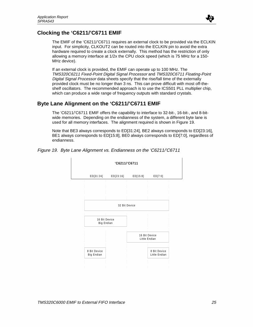
Byte Lane Alignment on the ‘C6211/’C6711 EMIF
The ‘C6211/’C6711 EMIF offers the capability to interface to 32-bit-, 16-bit-, and 8-bit-wide memories. Depending on the endianness of the system, a different byte lane isused for all memory interfaces. The alignment required is shown in Figure 19.
Note that BE3 always corresponds to ED[31:24], BE2 always corresponds to ED[23:16],BE1 always corresponds to ED[15:8], BE0 always corresponds to ED[7:0], regardless ofendianness.
Figure 19. Byte Lane Alignment vs. Endianness on the ‘C6211/’C6711
'C6211/'C6711
ED[31:24] ED[23:16] ED[15:8] ED[7:0]
8 Bit DeviceBig Endian
8 Bit DeviceLitt le Endian
16 Bit DeviceBig Endian
16 Bit DeviceLitt le Endian
32 Bit Device

Application ReportSPRA543
TMS320C6000 EMIF to External FIFO Interface 26
EMIF Registers
Control of the EMIF and the memory interfaces it supports is maintained through a set ofmemory-mapped registers within the EMIF. The memory-mapped registers are shown inTable 9.
Table 9. EMIF Memory-Mapped Registers
Byte Address Name
0x01800000 EMIF global control
0x01800004 EMIF CE1 space control
0x01800008 EMIF CE0 space control
0x0180000C Reserved
0x01800010 EMIF CE2 space control
0x01800014 EMIF CE3 space control
CE Space Control Registers
The four CE space control registers (Figure 20 and Figure 21) correspond to the four CEspaces supported by the EMIF. The MTYPE field identifies the memory type for thecorresponding CE space. If MTYPE selects SDRAM or SBSRAM, the remaining fields inthe register do not apply. If an asynchronous type is selected (ROM or 32-bitasynchronous), the remaining fields specify the shaping of the address and controlsignals for access to that space. Table 10 contains a more detailed description of theasynchronous configuration fields, which are used in the FIFO interface.
Figure 20. ‘C6201/’C6202/’C6701 EMIF CE(0/1/2/3) Space Control Register Diagram31 28 27 22 21 20 19 16
WRITE SETUP WRITE STROBE WRITE HOLD READ SETUPRW, +1111 RW, +111111 RW, +11 RW, +1111
15 14 13 8 7 6 4 3 2 1 0Reserved READ STROBE rsv MTYPE reserved READ HOLD
R, +11 RW, +111111 R, +0 RW, +010 R, +0 RW, +11
Figure 21. ‘C6211/’C6711 EMIF CE(0/1/2/3) Space Control Register Diagram31 28 27 22 21 20 19 16
WRITE SETUP WRITE STROBE WRITE HOLD READ SETUPRW, +1111 RW, +111111 RW, +11 RW, +1111
15 14 13 8 7 6 4 3 2 1 0TA READ STROBE MTYPE WrHld
MSB READ HOLD
R, +11 RW, +111111 RW, +010 RW, +0 RW, +11
Application ReportSPRA543
TMS320C6000 EMIF to External FIFO Interface 27
Table 10. EMIF CE(0/1/2/3) Space Control Registers Bitfield Description
Field DescriptionREAD SETUP
WRITE SETUP
Setup width. Number of clock† cycles of setup for address (EA) andbyte enables (/BE(0-3)) before read strobe (/ARE) or write strobe(/AWE) falling. On the first access to a CE space, this is also thesetup after /CE falling.
READ STROBE
WRITE STROBE
Strobe width. The width of read strobe (/ARE) and write strobe(/AWE) in clock* cycles.
READ HOLD
WRITE HOLD
Hold width. Number of clock† cycles that address (EA) and bytestrobes (/BE(0-3)) are held after read strobe (/ARE) or write strobe(/AWE) rising. These fields are extended by one bit on the‘C6211/’C6711.
MTYPE Memory Type
‘C6201/’C6202/’C6701 only:
MTYPE = 000b: 8-bit-wide ROM (CE1 only)
MTYPE = 001b: 16-bit-wide ROM (CE1 only)
MTYPE = 010b: 32-bit-wide asynchronous interface
‘C6211/’C6711 only:
MTYPE = 0000b: 8-bit-wide asynchronous interface
MTYPE = 0001b: 16-bit-wide asynchronous interface
MTYPE = 0010b: 32-bit-wide asynchronous interface
TA‡ Turnaround time. Controls the number of ECLKOUT cyclesbetween a read and a write or between two reads.
† Clock = CLKOUT1 for ‘C6201/’C6202/’C6701. Clock = ECLKOUT for ‘C6211/’C6711.‡ + Applies to ‘C6211/’C6711 only
Full Example for Read InterfaceThis section walks through the configuration steps required to implement TI’sSN74ALVC7806 strobed FIFO with the TMS320C6201B. The SN74ALVC7806 is a 256x 18 device with an access time of 18 ns and a maximum frequency of 40 MHz.
The following assumptions are made:
r The FIFO is used in address space CE0.
r CLKOUT1 = 200 MHz, therefore tcyc is 5 ns.
r The FIFO is used as a block buffer for transferring a set number of 128 word framesbetween two points.
Based on the assumptions, a flag scheme must be used that works efficiently underthese conditions. Because frames of one-half the FIFO depth are transferred at a time, itis convenient to use the HF flag in conjunction with the DMA to perform the transfers. Asmentioned earlier, if the HF flag is the sole means of triggering a transaction from theFIFO, there is a risk of becoming stuck in one-half the FIFO. To overcome this, it isnecessary to use a general-purpose input to also monitor the state of the HF flag.

Application ReportSPRA543
TMS320C6000 EMIF to External FIFO Interface 28
This example details both the asynchronous interface settings required to interface to thisspecific FIFO and the code and algorithm techniques used to monitor the FIFO statusand read and write to/from the FIFO. Although the asynchronous settings andprogrammable logic are specific to this FIFO, the remainder of this example can beapplied to most FIFOs, if the asynchronous settings and logic described above are used.
Hardware Interface
Figure 22 shows the interface between the EMIF and TI’s SN74ALVC7806.
Because in this example we want to transfer 128 words, we also want to have the FIFOsignal the CPU when this has occurred via an interrupt. Because interrupts for the ‘C6000are triggered on the rising edge (or falling edge but not both), the interrupt only informsthe CPU of a transition to half full. Therefore, to know what state the FIFO is in at alltimes, the TINP0 pin is used as a general-purpose input. The logic for this example is asfollows:
r UNCK = /CE0 + /ARE
r /OE = /CE0 + /AOE
r INT6 = HF
r TINP0 = HF
Thus, INT6 is set on a low-to-high transition of HF, which implies that it is set when thebuffer becomes half full. Monitoring the TINP0 pin can be accomplished to always knowthe state of the FIFO.
Figure 22. Read Interface for SN74ALVC7806
ExternalLogic
External MemoryInterface (EMIF)
/ARE
/CE3
/AOE
/AWE
ED[31:16]
ED[15:0]
StrobedFIFO
U N C K L D C K
/EF
Q[17:0] D[17:0]
H F
/FF
/OE
INT6
StrobedFIFO
L D C K
/EF
Q[17:0] D[17:0]
H F
/FF
TINP0
U N C K/OE
AF/AE
AF/AE

Application ReportSPRA543
TMS320C6000 EMIF to External FIFO Interface 29
Software Setup
Register Configuration
Table 11 through Table 14 summarize the timing characteristics of the ‘C6201B and theSN74ALVC7806 FIFO, which are used to calculate the values for the CE0 spaceconfiguration register. This data is taken from the TMS320C6201/6201B Fixed-PointDigital Signal Processors data sheet and the SN74ALVC7806 FIFO Data Sheet.
Table 11. EMIF Input Timing Requirement Definitions
TimingParameter
Definition Min Max
tsu Data setup time, read D before CLKOUT1 high 4 ns
th Data hold time, read D after CLKOUT1 high 0.8 ns
Table 12. EMIF—Output Timing Characteristics (Data, Address, Control)
TimingParameter
Definition Min Max
td Output delay time, CLKOUT1 high to output signal valid -0.2 ns 4 ns
Table 13. FIFO—Input Timing Requirement
TimingParameter
Definition Min Max
trp(m) Minimum required read pulse width 8 ns
tsu(m) Data setup time required by the FIFO for writes, write D before /WHigh
5 ns
th(m) Data hold time required by the FIFO for writes, write D after /W high 0
tens(m) Enable setup time, time required from /OE, /REN, /WEN low toUNCK high
5 ns
trc(m) Length of the read cycle 25 ns
Table 14. FIFO—Output Timing Characteristics
TimingParameter
Definition Min Max
toe(m) Output enable time, /OE low to output valid 10 ns
tacc(m) Access time, from RCLK or /RE to ED valid 18 ns
Table 15. External Logic Characteristics of SN74LVC32A
TimingParameter
Definition Min Max
tpl Logic propagation, time from input to external logic valid to outputvalid
1.5 ns 3.8 ns

Application ReportSPRA543
TMS320C6000 EMIF to External FIFO Interface 30
Read Calculations
r Setup ³ 1
SETUP = 1 cycle
r Setup + Strobe ³ (tdmax + tplmax + toe(m) + tsu)/tcyc
Therefore,
STROBE ³ (tdmax + tplmax + toe(m) + tsu)/tcyc - SETUP
= (4ns + 3.8ns + 10ns + 4ns)/5ns - 1 cycle
³ 3.4 cycles
STROBE = 4 cycles, increased by 1 cycle to attain desired timing margin ;margin = 3 ns
r Hold + Setup + Strobe ³ (tdmax + tplmax + tacc(m) + tsu)/tcyc
Therefore,
HOLD ³ (tdmax + tplmax + tacc(m) + tsu)/tcyc – Setup – Strobe
³ (4ns + 3.8ns + 18 ns + 4ns)/5ns – 1 cycle – 4 cycles
³ 1 cycles
HOLD = 2 cycle, rounded up to attain desired timing margin ; margin = 5 ns
r Strobe ³ (trp(m) )/tcyc
STROBE ³ 8 ns / 5 ns = 1.6 cycles, which is satisfied with previously calculated valueof 4 cycles.
Setup + Strobe + Hold ³ (trc(m) )/tcyc
Therefore,
SETUP + STROBE + HOLD ³ 25ns/5ns
³ 5 cycles, which is satisfied with the previously calculated value of 7 cycles.
r Hold ³ tih – (tdmin + tplmin + toez(m))
Hold ³ (0.8 ns – (-0.2ns + 1.5ns + 2 ns) / 5 ns ³ -0.5 cycles, which is satisfied withpreviously calculated value of 1 cycle.
Using the above calculations, the CE space control register can now be properlyconfigured. Figure 23 shows the CE0 space control register with the properly assignedvalues for each field. MTYPE = 010 identifies the memory in this address space as 32-bit-wide asynchronous memory; the other fields are used as calculated above. Noticethat because this example is for a read interface, the write parameters are all set to theirmaximum value.
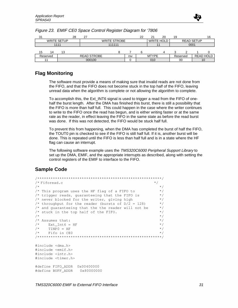
Application ReportSPRA543
TMS320C6000 EMIF to External FIFO Interface 31
Figure 23. EMIF CE0 Space Control Register Diagram for ‘780631 28 27 22 21 20 19 16
WRITE SETUP WRITE STROBE WRITE HOLD READ SETUP1111 111111 11 0001
15 14 13 8 7 6 4 3 2 1 0Reserved READ STROBE rsv MTYPE Reserved READ HOLD
11 000100 0 010 00 10
Flag Monitoring
The software must provide a means of making sure that invalid reads are not done fromthe FIFO, and that the FIFO does not become stuck in the top half of the FIFO, leavingunread data when the algorithm is complete or not allowing the algorithm to complete.
To accomplish this, the Ext_INT6 signal is used to trigger a read from the FIFO of one-half the burst length. After the DMA has finished this burst, there is still a possibility thatthe FIFO is more than half full. This could happen in the case where the writer continuesto write to the FIFO once the read has begun, and is either writing faster or at the samerate as the reader, in effect leaving the FIFO in the same state as before the read burstwas done. If this was not detected, the FIFO would be stuck half full.
To prevent this from happening, when the DMA has completed the burst of half the FIFO,the TOUT0 pin is checked to see if the FIFO is still half full. If it is, another burst will bedone. This is repeated until the FIFO is less than half full and is in a state where the HFflag can cause an interrupt.
The following software example uses the TMS320C6000 Peripheral Support Library toset up the DMA, EMIF, and the appropriate interrupts as described, along with setting thecontrol registers of the EMIF to interface to the FIFO.
Sample Code
/********************************************************//* Fiforead.c *//* *//* This program uses the HF flag of a FIFO to *//* trigger reads, guaranteeing that the FIFO is *//* never blocked for the writer, giving high *//* throughput for the reader (bursts of D/2 = 128) *//* and guaranteeing that the the reader will not be *//* stuck in the top half of the FIFO. *//* *//* Assumes that: *//* Ext_Int6 = HF *//* TINP0 = HF *//* Fifo in CE0 *//********************************************************/
#include <dma.h>#include <emif.h>#include <intr.h>#include <timer.h>
#define FIFO_ADDR 0x00400000#define BUFF_ADDR 0x80000000

Application ReportSPRA543
TMS320C6000 EMIF to External FIFO Interface 32
#define FIFO_DEPTH 256#define NUM_FRAMES 8
void set_EMIF();void set_DMA();void set_intr();interrupt void c_int06();interrupt void c_int08();int fifo_halffull();
int num_frames = NUM_FRAMES;int done = 0;
voidmain(){
set_EMIF();set_intr();set_DMA();
while (!done){// execute_user_code}
printf("DONE \n\n");}
/* This function sets up ce0 as ASRAM */void set_EMIF(){
/* Get default values for all EMIF registers */unsigned int g_ctrl = GET_REG(EMIF_GCTRL);unsigned int ce0_ctrl = GET_REG(EMIF_CE0_CTRL);unsigned int ce1_ctrl = GET_REG(EMIF_CE1_CTRL);unsigned int ce2_ctrl = GET_REG(EMIF_CE2_CTRL);unsigned int ce3_ctrl = GET_REG(EMIF_CE3_CTRL);unsigned int sdram_ctrl = GET_REG(EMIF_SDRAM_CTRL);unsigned int sdram_ref = GET_REG(EMIF_SDRAM_REF);
/* Configure CE0 as ASRAM for FIFO interface */LOAD_FIELD(&ce0_ctrl, MTYPE_32ASYNC, MTYPE , MTYPE_SZ );LOAD_FIELD(&ce0_ctrl, 1 , READ_SETUP , READ_SETUP_SZ );LOAD_FIELD(&ce0_ctrl, 4 , READ_STROBE , READ_STROBE_SZ );LOAD_FIELD(&ce0_ctrl, 2 , READ_HOLD , READ_HOLD_SZ );
/* Store EMIF Control Registers */emif_init(g_ctrl, ce0_ctrl, ce1_ctrl, ce2_ctrl, ce3_ctrl,
sdram_ctrl, sdram_ref);}
/* set up the DMA */void set_DMA(){
unsigned int channel = 0;unsigned int pri_ctrl= GET_REG(DMA0_PRIMARY_CTRL);unsigned int sec_ctrl= GET_REG(DMA0_SECONDARY_CTRL);unsigned int src_addr = 0;
Application ReportSPRA543
TMS320C6000 EMIF to External FIFO Interface 33
unsigned int dst_addr = 0;unsigned int trans_ctr= 0;
dma_reset();
/** Set DMA primary control register for channel 0 **/
LOAD_FIELD(&pri_ctrl, DMA_STOP_VAL , START , START_SZ);LOAD_FIELD(&pri_ctrl, DMA_ADDR_NO_MOD, SRC_DIR, SRC_DIR_SZ);LOAD_FIELD(&pri_ctrl, DMA_ADDR_INC , DST_DIR, DST_DIR_SZ);LOAD_FIELD(&pri_ctrl, DMA_ESIZE32 , ESIZE , ESIZE_SZ);SET_BIT(&pri_ctrl, PRI);SET_BIT(&pri_ctrl, TCINT);
/** Set DMA secondary control register for channel 0 **/LOAD_FIELD(&sec_ctrl, DMAC_BLOCK_COND, DMAC_EN, DMAC_EN_SZ);SET_BIT(&sec_ctrl, BLOCK_IE);
/** Set source address register **/src_addr = FIFO_ADDR;
/** Set destination address register **/dst_addr = BUFF_ADDR;
/** Set transfer counter **/LOAD_FIELD(&trans_ctr, FIFO_DEPTH/2, ELEMENT_COUNT, ELEMENT_COUNT_SZ);
/** Set the DMA registers **/dma_init(channel, pri_ctrl, sec_ctrl, src_addr, dst_addr,trans_ctr);
}
/****/* This routine uses the Peripheral Support Library functions/* to initialize the interrupt vector table and enable the required/* interrupts./****/voidset_intr(){
intr_init();intr_map(CPU_INT6, ISN_EXT_INT6);intr_map(CPU_INT8, ISN_DMA_INT0);intr_hook(c_int06, CPU_INT6);intr_hook(c_int08, CPU_INT8);
INTR_GLOBAL_ENABLE;INTR_ENABLE(CPU_INT_NMI);INTR_ENABLE(CPU_INT6);INTR_ENABLE(CPU_INT8);
}

Application ReportSPRA543
TMS320C6000 EMIF to External FIFO Interface 34
/****/* This routine checks the current state of the FIFO/* by monitoring the TINP0 pin./* Returns : 1 if HF flag is set indicating the FIFO is half full/* 0 if HF flag is not set, indicating less than half full./****/intfifo_halffull(){
int half_full ;
half_full = TINP_GET(0);return half_full;
}
/****/* This interrupt service routine is entered when the half full/* flag (on the Ext_Int6 pin) changes state from low to high,/* then kicks off a DMA transfer of 1/2 of the FIFO depth./****/interrupt voidc_int06() /* EXT_int6 */{
INTR_DISABLE(6); /* Disable interrupt 6, so that any toggling */ /* of the HF flag is disregarded until the DMA*/ /* transfer is complete. */
if (num_frames > 0){DMA_START(0); /* Starts the DMA transfer, if haven’t */
/* transferred the desired number of frames. */}
}
/****/* This interrupt service routine is entered when the DMA Block Cond/* is set, indicating that the DMA transfer has completed. This/* routine will check the current state of the FIFO. If the FIFO is/* still half full, it will start another DMA transfer, since a low to/* high transition will not be able to occur on Ext_Int6 (since HF is/* already high). This technique prevents the FIFO from becoming stuck/* half full./****interrupt voidc_int08() /* DMA Interrupt */{
int half_full;
num_frames--; /* Decrement frame counter */
RESET_BIT(DMA_SECONDARY_CTRL_ADDR(0), BLOCK_COND);* (unsigned int *) DMA_XFR_COUNTER_ADDR(0) = FIFO_DEPTH/2;
/* Check the state of the FIFO */half_full = fifo_halffull();
Application ReportSPRA543
TMS320C6000 EMIF to External FIFO Interface 35
if (num_frames > 0){if (half_full)
DMA_START(0); /* Start the DMA if the FIFO is */ /* still half full, and all the */
/* frames have not already been */else /* read, otherwise, */
INTR_ENABLE(6); /* enable interrupt 6, to detect */ /* the next rising edge of HF */
}else
done = 1;}
Full Example for Write InterfaceThis section will walk through the configuration steps required to implement a writeinterface between the TMS320C6201B and TI’s SN74ALVC7806 Strobed FIFO, which isa 256 x 18 device with an access time of 18 ns and a maximum frequency of 40 MHz.
The following assumptions will be made :
r The FIFO will be used in address space CE3.
r CLKOUT1 = 200 MHz, therefore tcyc is 5 ns.
r The FIFO will be used as a block buffer for transferring a set number of 128 wordframes between two points.
r The reader (on the opposite side) is slow compared to the ‘C6000 burst rate toasynchronous memory.
Based on the assumptions, a flag scheme must be used which will work efficiently underthese conditions. Since frames of ½ of the FIFO depth will be transferred at a time, it isconvenient to use the HF flag in conjunction with the DMA to perform the transfers. Aswas mentioned earlier, if the HF flag is the sole means of triggering a transaction from theFIFO, there is a risk of becoming stuck in one half of the FIFO.
However, from a system level, a designer can estimate at what rate each side (read orwrite) is able to access the FIFO. This example makes the assumption that the otherside of the FIFO is very slow compared to the write interface between the ‘C6000 and theFIFO. With this assumption, the FIFO interface can be greatly simplified compared to theprevious example. If there is no danger of 1) becoming stuck in one half of the FIFO or2) having the flag trigger back and forth in the middle of a burst, then the flag canautomatically trigger DMA transactions with no CPU intervention.
This example will detail both the asynchronous interface settings required to interface tothis specific FIFO and the code and algorithm techniques used to monitor the FIFO’sstatus and write to the FIFO.
Although the asynchronous settings and programmable logic are specific to this FIFO,the remainder of this example can be applied to most FIFOs if the asynchronous settingsand logic mentioned in this document are used.

Application ReportSPRA543
TMS320C6000 EMIF to External FIFO Interface 36
Hardware Interface
Figure 24 shows the interface between the EMIF and TI’s SN74ALVC7806. The onlydifference between this diagram and the generic diagram for strobed FIFOs is that TI’sdevice uses an active-high HF flag.
r LDCK = /CE3 + /AWE
r INT7 = ! HF
Thus, INT7 is set on a high-to-low transition of HF, which implies that it will be set whenthe buffer becomes less than half full.
Figure 24. Write Interface for SN74ALVC7806
ExternalLogic
External MemoryInterface (EMIF)
/ARE
/CEn
/AOE
/AWE
ED[31:16]
ED[15:0]
StrobedFIFO
L D C K U N C K
/EF
D[17:0] Q[17:0]
H F
/FF
/OE
INT7
StrobedFIFO
U N C K
/EF
D[17:0] Q[17:0]
H F
/FF
L D C K/OE

Application ReportSPRA543
TMS320C6000 EMIF to External FIFO Interface 37
Software Setup
Register Configuration
Table 16 through Table 18 summarize the timing characteristics of the ‘7806 FIFO forwrite cycles, which are used to calculate the values for the CE0 space configurationregister. This data is taken from the SN74ALVC7806 FIFO Data Sheet.
Table 16. EMIF—Output Timing Characteristics (Data, Address, Control)
TimingParameter
Definition Min Max
td Output delay time, CLKOUT1 high to output signal valid –0.2 ns 4 ns
Table 17. FIFO—Input Timing Requirement
TimingParameter
Definition Min Max
twp(m) Minimum required write pulse width 8 ns
tsu(m) Data setup time required by the FIFO for writes, write D before /WHigh
5 ns
tih(m) Data hold time required by the FIFO for writes, write D after LDCKHigh
0 ns
tens(m) Enable setup time, time required from /OE, /REN, /WEN low toUNCK high
5 ns
twc(m) Length of the write cycle 25 ns
Table 18. External Logic Characteristics of SN74LVC32A
TimingParameter
Definition Min Max
tpl Logic propagation, time from input to external logic valid to outputvalid
1.5 ns 3.8 ns
Write Calculations
r Setup ³ 1
SETUP = 1 cycle
r Hold ³ (tskew + tplmax + tih(m))/tcyc
HOLD ³ (2ns + 3.8 ns + 0 ns)/ 5 ns = 1.2,
³ 1.2 cycles
HOLD = 2 cycles, increased by 1 cycle to attain desired timing margin
r Setup + Strobe + Hold ³ (twc(m))/tcyc
Therefore,
Strobe ³ twc(m)/tcyc - SETUP – HOLD = 25ns/5ns – 1 cycles – 2 cycles
³ 2 cycles
Strobe = 3 cycles, increased by 1 cycle to attain desired timing margin
Application ReportSPRA543
TMS320C6000 EMIF to External FIFO Interface 38
r Strobe ³ (twp(m) )/tcyc
STROBE ³ twp(m)/tcyc= 8ns/5ns = 1.6
³ 1.6 cycles, satisfied by previous constraints.
r Setup + Strobe ³ (tsu(m) + tskew - tplmin)/tcyc
SETUP + STROBE ³ 5.5 ns = 1.1 cycles, therefore this constraint is satisfied.
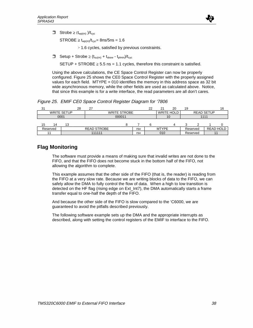
Using the above calculations, the CE Space Control Register can now be properlyconfigured. Figure 25 shows the CE0 Space Control Register with the properly assignedvalues for each field. MTYPE = 010 identifies the memory in this address space as 32 bitwide asynchronous memory, while the other fields are used as calculated above. Notice,that since this example is for a write interface, the read parameters are all don’t cares.
Figure 25. EMIF CE0 Space Control Register Diagram for ‘780631 28 27 22 21 20 19 16
WRITE SETUP WRITE STROBE WRITE HOLD READ SETUP0001 000011 10 1111
15 14 13 8 7 6 4 3 2 1 0Reserved READ STROBE rsv MTYPE Reserved READ HOLD
11 111111 rsv 010 Reserved 11
Flag Monitoring
The software must provide a means of making sure that invalid writes are not done to theFIFO, and that the FIFO does not become stuck in the bottom half of the FIFO, notallowing the algorithm to complete.
This example assumes that the other side of the FIFO (that is, the reader) is reading fromthe FIFO at a very slow rate. Because we are writing blocks of data to the FIFO, we cansafely allow the DMA to fully control the flow of data. When a high to low transition isdetected on the HF flag (rising edge on Ext_Int7), the DMA automatically starts a frametransfer equal to one-half the depth of the FIFO.
And because the other side of the FIFO is slow compared to the ‘C6000, we areguaranteed to avoid the pitfalls described previously.
The following software example sets up the DMA and the appropriate interrupts asdescribed, along with setting the control registers of the EMIF to interface to the FIFO.

Application ReportSPRA543
TMS320C6000 EMIF to External FIFO Interface 39
Sample Code
/********************************************************//* Fifowrite.c *//* *//* This program uses the HF flag of a FIFO to *//* trigger writes, guaranteeing that the FIFO is *//* never blocked for the reader, and giving high *//* throughput for the writer (bursts of D/2 = 128) *//* *//* Assumes that: *//* Ext_Int7 = !HF *//* Fifo in CE3 *//********************************************************/
#include <dma.h>#include <emif.h>#include <intr.h>
#define FIFO_ADDR 0x03000000#define BUFF_ADDR 0x80000000#define FIFO_DEPTH 256#define NUM_FRAMES 8#define BUFF_END BUFF_ADDR + NUM_FRAMES * FIFO_DEPTH/2
void set_EMIF();void set_DMA();void set_intr();interrupt void c_int08();
int done = 0;
voidmain(){
set_EMIF();set_intr();set_DMA();
while (!done){// execute_user_code}
printf("DONE \n\n");}

Application ReportSPRA543
TMS320C6000 EMIF to External FIFO Interface 40
/* This function sets up ce3 as ASRAM */void set_EMIF(){
/* Get default values for all EMIF registers */unsigned int g_ctrl = GET_REG(EMIF_GCTRL);unsigned int ce0_ctrl = GET_REG(EMIF_CE0_CTRL);unsigned int ce1_ctrl = GET_REG(EMIF_CE1_CTRL);unsigned int ce2_ctrl = GET_REG(EMIF_CE2_CTRL);unsigned int ce3_ctrl = GET_REG(EMIF_CE3_CTRL);unsigned int sdram_ctrl = GET_REG(EMIF_SDRAM_CTRL);unsigned int sdram_ref = GET_REG(EMIF_SDRAM_REF);
/* Configure CE3 as ASRAM for FIFO interface */LOAD_FIELD(&ce3_ctrl, MTYPE_32ASYNC, MTYPE ,MTYPE_SZ );LOAD_FIELD(&ce3_ctrl, 1 , WRITE_SETUP ,WRITE_SETUP_SZ );LOAD_FIELD(&ce3_ctrl, 3 , WRITE_STROBE,WRITE_STROBE_SZ );LOAD_FIELD(&ce3_ctrl, 2 , WRITE_HOLD ,WRITE_HOLD_SZ );
/* Store EMIF Control Registers */emif_init(g_ctrl, ce0_ctrl, ce1_ctrl, ce2_ctrl, ce3_ctrl,
sdram_ctrl, sdram_ref);}
/* set up the DMA */void set_DMA(){
unsigned int channel = 0;unsigned int pri_ctrl = GET_REG(DMA0_PRIMARY_CTRL);unsigned int sec_ctrl = GET_REG(DMA0_SECONDARY_CTRL);unsigned int src_addr = 0;unsigned int dst_addr = 0;unsigned int trans_ctr = 0;unsigned int dma_gcr = 0;unsigned int dma_gcra = 0;unsigned int dma_gcrb = 0;unsigned int dma_gndxa = 0;unsigned int dma_gndxb = 0;unsigned int dma_gaddra = 0;unsigned int dma_gaddrb = 0;unsigned int dma_gaddrc = 0;unsigned int dma_gaddrd = 0;
dma_reset();
/** Set DMA primary control register for channel 0 **//** Sets a frame synch'ed transfer, which is synchronized **//** to Ext_Int7 (ie !HF). **/LOAD_FIELD(&pri_ctrl, DMA_START_VAL , START , START_SZ);LOAD_FIELD(&pri_ctrl, DMA_ADDR_INC , SRC_DIR, SRC_DIR_SZ);LOAD_FIELD(&pri_ctrl, DMA_ADDR_NO_MOD, DST_DIR, DST_DIR_SZ); LOAD_FIELD(&pri_ctrl, DMA_ESIZE32 , ESIZE , ESIZE_SZ);LOAD_FIELD(&pri_ctrl, SEN_EXT_INT7 , RSYNC , RSYNC_SZ);SET_BIT(&pri_ctrl, PRI);SET_BIT(&pri_ctrl, TCINT);SET_BIT(&pri_ctrl, FS);
/** Set DMA secondary control register for channel 0 **/LOAD_FIELD(&sec_ctrl, DMAC_BLOCK_COND, DMAC_EN, DMAC_EN_SZ);
Application ReportSPRA543
TMS320C6000 EMIF to External FIFO Interface 41
SET_BIT(&sec_ctrl, BLOCK_IE);
/** Set source address register **/src_addr = BUFF_ADDR;
/** Set destination address register **/dst_addr = FIFO_ADDR;
/** Set transfer counter **/LOAD_FIELD(&trans_ctr,FIFO_DEPTH/2,ELEMENT_COUNT, ELEMENT_COUNT_SZ);LOAD_FIELD(&trans_ctr, NUM_FRAMES ,FRAME_COUNT , FRAME_COUNT_SZ );
/** Set transfer count reload value **/dma_gcra = FIFO_DEPTH/2;
/** Set global DMA values **/dma_global_init(dma_gcr, dma_gcra, dma_gcrb, dma_gndxa, dma_gndxb,
dma_gaddra, dma_gaddrb, dma_gaddrc, dma_gaddrd);
/** Set the DMA registers for channel 0**/dma_init(channel, pri_ctrl, sec_ctrl, src_addr, dst_addr,trans_ctr);
}
/****/* This routine uses the Peripheral Support Library functions/* to initialize the interrupt vector table and enable the required/* interrupts./****/
voidset_intr(){
intr_init();intr_map(CPU_INT8, ISN_DMA_INT0);intr_hook(c_int08, CPU_INT8);
INTR_GLOBAL_ENABLE;INTR_ENABLE(CPU_INT_NMI);INTR_ENABLE(CPU_INT8);
}
/****/* This interrupt service routine is entered when the DMA Block Cond/* is set, indicating that the DMA transfers have completed. Once every/* frame is completed, the 'done' flag is set, indicating to the CPU,/* that the transfer has been completed./****/interrupt voidc_int08() /* DMA Interrupt */{
done = 1;}
Application ReportSPRA543
TMS320C6000 EMIF to External FIFO Interface 42
ReferencesTMS320C6201/6201B Fixed-Point Digital Signal Processors Data Sheet, Literature
number SPRS051, April 1999, Texas Instruments.
TMS320C6202 Fixed-Point Digital Signal Processor Data Sheet, Literature numberSPRS072, January 1999, Texas Instruments.
TMS320C6211 Fixed-Point Digital Signal Processor Data Sheet, Literature numberSPRS073, March 1999, Texas Instruments.
TMS320C6701 Floating-Point Digital Signal Processor Data Sheet, Literature numberSPRS067, March 1999, Texas Instruments.
TMS320C6711 Floating-Point Digital Signal Processor Data Sheet, Literature numberSPRS088, March 1999, Texas Instruments.
TMS320C6000 Peripherals Reference Guide, Literature number SPRU190, March 1999,Texas Instruments.
TMS320C6000 Peripheral Support Library Programmers Reference, Literature numberSPRU273, June 1998, Texas Instruments.
SN74ALVC7806 256 x 18 Low Power FIFO Memory Data Sheet, April 1998, Literaturenumber, SCAS591
SN74ALVC7805 256 x 18 Low Power Clocked FIFO Memory Data Sheet, April 1998,Literature number SCAS593

Application ReportSPRA543
TMS320C6000 EMIF to External FIFO Interface 43
TI Contact Numbers
INTERNET
TI Semiconductor Home Pagewww.ti.com/sc
TI Distributorswww.ti.com/sc/docs/distmenu.htm
PRODUCT INFORMATION CENTERS
AmericasPhone +1(972) 644-5580Fax +1(972) 480-7800Email [email protected]
Europe, Middle East, and AfricaPhone
Deutsch +49-(0) 8161 80 3311English +44-(0) 1604 66 3399Español +34-(0) 90 23 54 0 28Francais +33-(0) 1-30 70 11 64Italiano +33-(0) 1-30 70 11 67
Fax +44-(0) 1604 66 33 34Email [email protected]
International +81-3-3344-5311Domestic 0120-81-0026
FaxInternational +81-3-3344-5317Domestic 0120-81-0036
Email [email protected]
AsiaPhone
International +886-2-23786800Domestic
Australia 1-800-881-011TI Number -800-800-1450
China 10810TI Number -800-800-1450
Hong Kong 800-96-1111TI Number -800-800-1450
India 000-117TI Number -800-800-1450
Indonesia 001-801-10TI Number -800-800-1450
Korea 080-551-2804Malaysia 1-800-800-011
TI Number -800-800-1450New Zealand 000-911
TI Number -800-800-1450Philippines 105-11
TI Number -800-800-1450Singapore 800-0111-111
TI Number -800-800-1450Taiwan 080-006800Thailand 0019-991-1111
TI Number -800-800-1450Fax 886-2-2378-6808Email [email protected]
TI is a trademark of Texas Instruments Incorporated.
Other brands and names are the property of their respective owners.
Application ReportSPRA543
TMS320C6000 EMIF to External FIFO Interface 44
IMPORTANT NOTICE
Texas Instruments and its subsidiaries (TI) reserve the right to make changes to theirproducts or to discontinue any product or service without notice, and advise customers toobtain the latest version of relevant information to verify, before placing orders, thatinformation being relied on is current and complete. All products are sold subject to theterms and conditions of sale supplied at the time of order acknowledgement, includingthose pertaining to warranty, patent infringement, and limitation of liability.
TI warrants performance of its semiconductor products to the specifications applicable atthe time of sale in accordance with TI's standard warranty. Testing and other qualitycontrol techniques are utilized to the extent TI deems necessary to support this warranty.Specific testing of all parameters of each device is not necessarily performed, exceptthose mandated by government requirements.
CERTAIN APPLICATIONS USING SEMICONDUCTOR PRODUCTS MAY INVOLVEPOTENTIAL RISKS OF DEATH, PERSONAL INJURY, OR SEVERE PROPERTY ORENVIRONMENTAL DAMAGE (“CRITICAL APPLICATIONS"). TI SEMICONDUCTORPRODUCTS ARE NOT DESIGNED, AUTHORIZED, OR WARRANTED TO BESUITABLE FOR USE IN LIFE-SUPPORT DEVICES OR SYSTEMS OR OTHERCRITICAL APPLICATIONS. INCLUSION OF TI PRODUCTS IN SUCH APPLICATIONSIS UNDERSTOOD TO BE FULLY AT THE CUSTOMER'S RISK.
In order to minimize risks associated with the customer's applications, adequate designand operating safeguards must be provided by the customer to minimize inherent orprocedural hazards.
TI assumes no liability for applications assistance or customer product design. TI doesnot warrant or represent that any license, either express or implied, is granted under anypatent right, copyright, mask work right, or other intellectual property right of TI coveringor relating to any combination, machine, or process in which such semiconductorproducts or services might be or are used. TI's publication of information regarding anythird party's products or services does not constitute TI's approval, warranty, orendorsement thereof.
Copyright Ó 1999 Texas Instruments Incorporated