Ti Jtag Tutor
130
Semiconductor Group 1997 Primer
-
Upload
joseph-mathew -
Category
Documents
-
view
65 -
download
2
description
JTAG Tutor
Transcript of Ti Jtag Tutor
� �� ����������� �����������
Semiconductor Group1997Printed in U.S.A.1096–AL
SSYA002C
Primer
i
IEEE Std 1149.1(JTAG) Testability
Primer

ii Contents
IMPORTANT NOTICE
Texas Instruments (TI) reserves the right to make changes to itsproducts or to discontinue any semiconductor product or servicewithout notice, and advises its customers to obtain the latest versionof relevant information to verify, before placing orders, that theinformation being relied on is current.
TI warrants performance of its semiconductor products and relatedsoftware to the specifications applicable at the time of sale inaccordance with TI’s standard warranty. Testing and other qualitycontrol techniques are utilized to the extent TI deems necessary tosupport this warranty. Specific testing of all parameters of eachdevice is not necessarily performed, except those mandated bygovernment requirements.
Certain applications using semiconductor products may involvepotential risks of death, personal injury, or severe property orenvironmental damage (“Critical Applications”).
TI SEMICONDUCTOR PRODUCTS ARE NOT DESIGNED,INTENDED, AUTHORIZED, OR WARRANTED TO BE SUITABLEFOR USE IN LIFE-SUPPORT APPLICATIONS, DEVICES ORSYSTEMS OR OTHER CRITICAL APPLICATIONS.
Inclusion of TI products in such applications is understood to be fullyat the risk of the customer. Use of TI products in such applicationsrequires the written approval of an appropriate TI officer. Questionsconcerning potential risk applications should be directed to TIthrough a local SC sales office.
In order to minimize risks associated with the customer’sapplications, adequate design and operating safeguards should beprovided by the customer to minimize inherent or proceduralhazards.
TI assumes no liability for applications assistance, customerproduct design, software performance, or infringement of patentsor services described herein. Nor does TI warrant or represent thatany license, either express or implied, is granted under any patentright, copyright, mask work right, or other intellectual property rightof TI covering or relating to any combination, machine, or processin which such semiconductor products or services might be or areused.
Copyright 1996, Texas Instruments Incorporated
iii
TRADEMARKS
ASSET is a trademark of ASSET InterTech Incorporated.
DEC is trademark of Digital Equipment Corporation.
Ethernet is a trademark of Xerox Corporation.
IBM is a trademark of International Business MachinesCorporation.
Microsoft is a registered trademark of Microsoft Corporation.
Scan Engine, ThunderCELL, ThunderLAN, TI, UBT, andWidebus are trademarks of Texas Instruments Incorporated.
UNIX is a registered trademark in the United States and othercountries, licensed exclusively through X/Open CompanyLimited.
SUPPORT
Device Boundary-Scan Description Language (BSDL) filesand other information regarding Texas Instruments IEEE Std1149.1/JTAG/boundary-scan products are maintained on theWorld-Wide Web at URL http://www.ti.com/sc/docs/jtag/jtaghome.htm; or, on the main Texas Instruments home pageat URL http://www.ti.com. Search for keywords JTAGand testability.
v
Contents
Introduction 1-1. . . . . . . . . . . . . . . . . . . . . . . . . . . . . . . . . . . . . Overall Rationale for Design for Test 1-2. . . . . . . . . . . . . . . . . Reduced Cost and Higher Quality 1-3. . . . . . . . . . . . . . . . . . . Benefits Over Standard Test Methods 1-3. . . . . . . . . . . . . . . . Standard Test Solutions Versus Proprietary Solutions 1-5. . . An Industry Standard — IEEE Std 1149.1-1990
(JTAG) 1-5. . . . . . . . . . . . . . . . . . . . . . . . . . . . . . . . . . . . . .
Benefits of Testability 2-1. . . . . . . . . . . . . . . . . . . . . . . . . . . . . Traditional Testing 2-1. . . . . . . . . . . . . . . . . . . . . . . . . . . . . . . . . Efficient Testing 2-1. . . . . . . . . . . . . . . . . . . . . . . . . . . . . . . . . . . Lower Cost for Testing 2-1. . . . . . . . . . . . . . . . . . . . . . . . . . . . . Production Time Savings 2-2. . . . . . . . . . . . . . . . . . . . . . . . . . . Easier Board-Level Isolation 2-2. . . . . . . . . . . . . . . . . . . . . . . . Simple Access to Circuits 2-2. . . . . . . . . . . . . . . . . . . . . . . . . . .
Boundary-Scan Architecture and IEEE Std 1149.1 3-1. . . . . . . . . . . . . . . . . . . . . . . . . .
Boundary-Scan Overview 3-2. . . . . . . . . . . . . . . . . . . . . . . . . . . Test Interface and Boundary-Scan Architecture 3-3. . . . . . . . Test Access Port and Operation 3-5. . . . . . . . . . . . . . . . . . . . . IEEE Std 1149.1 Registers 3-8. . . . . . . . . . . . . . . . . . . . . . . . . .
Instruction Register (Required) 3-8. . . . . . . . . . . . . . . . . . Data Registers 3-9. . . . . . . . . . . . . . . . . . . . . . . . . . . . . . .
IEEE Std 1149.1 Required Instructions 3-12. . . . . . . . . . . . . . BYPASS Instruction 3-12. . . . . . . . . . . . . . . . . . . . . . . . . . SAMPLE/PRELOAD Instruction 3-12. . . . . . . . . . . . . . . . EXTEST Instruction 3-13. . . . . . . . . . . . . . . . . . . . . . . . . .
IEEE Std 1149.1 Optional Instructions 3-13. . . . . . . . . . . . . . . INTEST Instruction 3-13. . . . . . . . . . . . . . . . . . . . . . . . . . . RUNBIST Instruction 3-13. . . . . . . . . . . . . . . . . . . . . . . . . CLAMP Instruction 3-13. . . . . . . . . . . . . . . . . . . . . . . . . . . HIGHZ Instruction 3-14. . . . . . . . . . . . . . . . . . . . . . . . . . . . IDCODE Instruction 3-14. . . . . . . . . . . . . . . . . . . . . . . . . . USERCODE Instruction 3-14. . . . . . . . . . . . . . . . . . . . . . .
Obtaining IEEE Std 1149.1-1990 3-15. . . . . . . . . . . . . . . . . . .
vi Contents
Using DFT in ASICs 4-1. . . . . . . . . . . . . . . . . . . . . . . . . . . . . . Design-for-Test Considerations 4-1. . . . . . . . . . . . . . . . . . . . . . The Need for Testability 4-2. . . . . . . . . . . . . . . . . . . . . . . . . . . . Test-Time Cost 4-3. . . . . . . . . . . . . . . . . . . . . . . . . . . . . . . . . . . . Time to Market 4-3. . . . . . . . . . . . . . . . . . . . . . . . . . . . . . . . . . . . Fault Coverage and Cost of Ownership 4-5. . . . . . . . . . . . . . . Developing Testability Strategies 4-8. . . . . . . . . . . . . . . . . . . .
Data Formats 5-1. . . . . . . . . . . . . . . . . . . . . . . . . . . . . . . . . . . . Boundary-Scan Description Language (BSDL) 5-1. . . . . . . .
How BSDL Is Used 5-1. . . . . . . . . . . . . . . . . . . . . . . . . . . . Elements of BSDL 5-2. . . . . . . . . . . . . . . . . . . . . . . . . . . . Verifying BSDL Accuracy 5-4. . . . . . . . . . . . . . . . . . . . . . . Potential BSDL Errors 5-5. . . . . . . . . . . . . . . . . . . . . . . . . How to Receive the BSDL Specification 5-5. . . . . . . . . . Obtaining BSDL for TI Devices 5-5. . . . . . . . . . . . . . . . . .
Hierarchical Scan Description Language (HSDL) 5-6. . . . . . Elements of HSDL 5-6. . . . . . . . . . . . . . . . . . . . . . . . . . . . How to Receive the HSDL Specification 5-8. . . . . . . . . .
Serial Vector Format (SVF) 5-9. . . . . . . . . . . . . . . . . . . . . . . . . SVF Structure 5-10. . . . . . . . . . . . . . . . . . . . . . . . . . . . . . . Default State Transitions 5-12. . . . . . . . . . . . . . . . . . . . . . SVF Example 5-15. . . . . . . . . . . . . . . . . . . . . . . . . . . . . . . How to Receive the SVF Specification 5-16. . . . . . . . . .
Suggested Design-for-Test Flow 6-1. . . . . . . . . . . . . . . . . . . Test Requirements 6-2. . . . . . . . . . . . . . . . . . . . . . . . . . . . . . . . Built-In Self-Test (BIST) Methodology 6-3. . . . . . . . . . . . . . . . Internal Scan Test Methodology 6-3. . . . . . . . . . . . . . . . . . . . . Design Effort 6-4. . . . . . . . . . . . . . . . . . . . . . . . . . . . . . . . . . . . . .
IC Design Implementation 6-4. . . . . . . . . . . . . . . . . . . . . . IC Simulation 6-6. . . . . . . . . . . . . . . . . . . . . . . . . . . . . . . . . Using SVF for IC Design Validation 6-6. . . . . . . . . . . . . . Data Passed to Board Designer 6-7. . . . . . . . . . . . . . . . .
Board Design 6-8. . . . . . . . . . . . . . . . . . . . . . . . . . . . . . . . . . . . . Constraints 6-8. . . . . . . . . . . . . . . . . . . . . . . . . . . . . . . . . . . . . . . Partitioned Scan Path 6-8. . . . . . . . . . . . . . . . . . . . . . . . . . . . . .
vii
Board Validation/Manufacturing Test 6-9. . . . . . . . . . . . . . . . . Summary 6-10. . . . . . . . . . . . . . . . . . . . . . . . . . . . . . . . . . . . . . . .
Applications 7-1. . . . . . . . . . . . . . . . . . . . . . . . . . . . . . . . . . . . . Board-Etch and Solder-Joint Testing 7-1. . . . . . . . . . . . . . . . .
Solution 7-1. . . . . . . . . . . . . . . . . . . . . . . . . . . . . . . . . . . . . Detailed Description 7-2. . . . . . . . . . . . . . . . . . . . . . . . . . . Summary 7-4. . . . . . . . . . . . . . . . . . . . . . . . . . . . . . . . . . . .
Cluster Testing 7-5. . . . . . . . . . . . . . . . . . . . . . . . . . . . . . . . . . . . Solution 7-5. . . . . . . . . . . . . . . . . . . . . . . . . . . . . . . . . . . . . Detailed Description 7-5. . . . . . . . . . . . . . . . . . . . . . . . . . . Summary 7-6. . . . . . . . . . . . . . . . . . . . . . . . . . . . . . . . . . . .
Board-Edge Connector Testing 7-7. . . . . . . . . . . . . . . . . . . . . . Solution 7-7. . . . . . . . . . . . . . . . . . . . . . . . . . . . . . . . . . . . . Detailed Description 7-7. . . . . . . . . . . . . . . . . . . . . . . . . . . Summary 7-9. . . . . . . . . . . . . . . . . . . . . . . . . . . . . . . . . . . .
ASIC Verification 7-10. . . . . . . . . . . . . . . . . . . . . . . . . . . . . . . . . Solution 7-10. . . . . . . . . . . . . . . . . . . . . . . . . . . . . . . . . . . . Detailed Description 7-10. . . . . . . . . . . . . . . . . . . . . . . . . . Summary 7-11. . . . . . . . . . . . . . . . . . . . . . . . . . . . . . . . . . .
Memory-Testing Techniques 7-12. . . . . . . . . . . . . . . . . . . . . . . Solution 7-12. . . . . . . . . . . . . . . . . . . . . . . . . . . . . . . . . . . . Detailed Description 7-12. . . . . . . . . . . . . . . . . . . . . . . . . . Summary 7-16. . . . . . . . . . . . . . . . . . . . . . . . . . . . . . . . . . .
Backplane Multidrop Environment 7-17. . . . . . . . . . . . . . . . . . Solution 7-19. . . . . . . . . . . . . . . . . . . . . . . . . . . . . . . . . . . . Detailed Description 7-20. . . . . . . . . . . . . . . . . . . . . . . . . . Summary 7-21. . . . . . . . . . . . . . . . . . . . . . . . . . . . . . . . . . .
Embedded Applications 7-21. . . . . . . . . . . . . . . . . . . . . . . . . . . Solution 7-21. . . . . . . . . . . . . . . . . . . . . . . . . . . . . . . . . . . . Detailed Description 7-21. . . . . . . . . . . . . . . . . . . . . . . . . . Summary 7-23. . . . . . . . . . . . . . . . . . . . . . . . . . . . . . . . . . .
Boundary-Scan Test Flow 7-24. . . . . . . . . . . . . . . . . . . . . . . . . Solution 7-24. . . . . . . . . . . . . . . . . . . . . . . . . . . . . . . . . . . . Detailed Description 7-24. . . . . . . . . . . . . . . . . . . . . . . . . . Summary 7-28. . . . . . . . . . . . . . . . . . . . . . . . . . . . . . . . . . .
viii Contents
Product Summary 8-1. . . . . . . . . . . . . . . . . . . . . . . . . . . . . . . . IEEE Std 1149.1-Compatible Components 8-1. . . . . . . . . . . .
Highlights 8-1. . . . . . . . . . . . . . . . . . . . . . . . . . . . . . . . . . . . IEEE Std 1149.1 (JTAG) Boundary-Scan Logic 8-2. . . . . . . .
Bus Interface 8-3. . . . . . . . . . . . . . . . . . . . . . . . . . . . . . . . . Universal Bus Transceiver (UBT ) 8-4. . . . . . . . . . . . . . Scan Support 8-5. . . . . . . . . . . . . . . . . . . . . . . . . . . . . . . . .
Other Support and Learning Products 9-1. . . . . . . . . . . . . Scan Educator 9-1. . . . . . . . . . . . . . . . . . . . . . . . . . . . . . . . . . . . Scan Board 9-1. . . . . . . . . . . . . . . . . . . . . . . . . . . . . . . . . . . . . . .
Flexibility 9-2. . . . . . . . . . . . . . . . . . . . . . . . . . . . . . . . . . . . Compatibility 9-3. . . . . . . . . . . . . . . . . . . . . . . . . . . . . . . . . Supporting Documentation Included 9-3. . . . . . . . . . . . .
CD-ROM 9-3. . . . . . . . . . . . . . . . . . . . . . . . . . . . . . . . . . . . . . . . . Testability Video Tape 9-4. . . . . . . . . . . . . . . . . . . . . . . . . . . . . . Appendix A — Abbreviations/Acronyms A-1. . . . . . . . . . . Appendix B — Glossary B-1. . . . . . . . . . . . . . . . . . . . . . . . . . Appendix C — References C-1. . . . . . . . . . . . . . . . . . . . . . . . Appendix D — Internet Starting Points D-1. . . . . . . . . . . . .
Index Index-1. . . . . . . . . . . . . . . . . . . . . . . . . . . . . . . . . . . . . . . .
ix
Illustrations
1-1 Chip Through System-Level Test 1-1. . . . . . . . . . . . . . 2-1 Boundary-Scan Testing Using the
IEEE Std 1149.1 Bus 2-3. . . . . . . . . . . . . . . . . . . . . . . . . 3-1 Boundary-Scan Example 3-2. . . . . . . . . . . . . . . . . . . . . 3-2 Boundary-Scan Architecture 3-4. . . . . . . . . . . . . . . . . . 3-3 TAP Controller State Diagram 3-5. . . . . . . . . . . . . . . . . 3-4 TAP Control Output Interconnect Diagram 3-7. . . . . . 3-5 General Instruction Register Architecture 3-8. . . . . . . 3-6 Test Data Register Architecture 3-10. . . . . . . . . . . . . . . 3-7 Conceptual View of a
Control-and-Observe BSC 3-11. . . . . . . . . . . . . . . . . . . 3-8 Device Identification Register Structure 3-11. . . . . . . . 4-1 Fault Grade Versus Development Time 4-3. . . . . . . . . 4-2 Economic Trade-Off for a Testable Design 4-4. . . . . . 4-3 Defect Level Versus Fault Coverage 4-5. . . . . . . . . . . 4-4 Motorola and Delco Study Results 4-6. . . . . . . . . . . . . 4-5 ASIC ppm Versus PCB ppm Rate 4-7. . . . . . . . . . . . . . 4-6 Cost of Ownership 4-8. . . . . . . . . . . . . . . . . . . . . . . . . . . 4-7 Testability Development Flow 4-11. . . . . . . . . . . . . . . . 5-1 Scan Path of Six ICs 5-10. . . . . . . . . . . . . . . . . . . . . . . . 6-1 Initial DFT Concerns 6-1. . . . . . . . . . . . . . . . . . . . . . . . . 6-2 Designing Testability for ASICs and Boards 6-4. . . . . 6-3 Debug and Verification of a
Boundary-Scan Design 6-7. . . . . . . . . . . . . . . . . . . . . . . 7-1 Etch/Interconnect Testing 7-2. . . . . . . . . . . . . . . . . . . . . 7-2 Open-Etch Condition 7-3. . . . . . . . . . . . . . . . . . . . . . . . . 7-3 Open-Solder-Joint Condition 7-3. . . . . . . . . . . . . . . . . . 7-4 Short-to-Ground Condition 7-3. . . . . . . . . . . . . . . . . . . . 7-5 Bond-Wire Testing 7-4. . . . . . . . . . . . . . . . . . . . . . . . . . . 7-6 Cluster Testing 7-5. . . . . . . . . . . . . . . . . . . . . . . . . . . . . . 7-7 Backplane Open-Circuit Fault 7-8. . . . . . . . . . . . . . . . . 7-8 PWB Connector Fault 7-8. . . . . . . . . . . . . . . . . . . . . . . . 7-9 Backplane Short-to-Ground Fault 7-9. . . . . . . . . . . . . . 7-10 Block Diagram of Simplified
Boundary-Scannable RAM Interface 7-13. . . . . . . . . . 7-11 Testing Embedded RAM 7-15. . . . . . . . . . . . . . . . . . . . .
x Contents
7-12 Testing Embedded ROM 7-16. . . . . . . . . . . . . . . . . . . . 7-13 Backplane Ring Configuration 7-18. . . . . . . . . . . . . . . . 7-14 Backplane Star Configuration 7-19. . . . . . . . . . . . . . . . 7-15 Backplane With ASP-Equipped Boards 7-20. . . . . . . . 7-16 General Boundary-Scan Test 7-25. . . . . . . . . . . . . . . . . 7-17 Assembly Verification Flow 7-26. . . . . . . . . . . . . . . . . . 7-18 Automated Functional Verification and
Fault Detection 7-27. . . . . . . . . . . . . . . . . . . . . . . . . . . . . 7-19 Interactive Verification and Fault Isolation 7-28. . . . . . 8-1 TI’s Family of IEEE Std 1149.1 (JTAG)
Boundary-Scan Logic 8-2. . . . . . . . . . . . . . . . . . . . . . . .

xi
Tables
1-1 High-Technology Product Scenarios 1-3. . . . . . . . . . . . . 1-2 Time to Develop Test Programs (in Man-Months) 1-4. . 5-1 SVF TAP State Names 5-13. . . . . . . . . . . . . . . . . . . . . . . 5-2 Stable-State Path Examples 5-14. . . . . . . . . . . . . . . . . . 7-1 Access Rates of IEEE Std 1149.1 Devices
With and Without BIST 7-14. . . . . . . . . . . . . . . . . . . . . . . 8-1 IEEE Std 1149.1 UBTs Replace
50+ Bus Functions 8-5. . . . . . . . . . . . . . . . . . . . . . . . . . . .
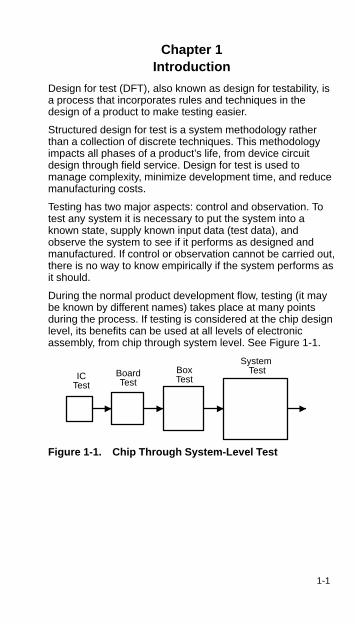
1-1
Chapter 1Introduction
Design for test (DFT), also known as design for testability, isa process that incorporates rules and techniques in thedesign of a product to make testing easier.
Structured design for test is a system methodology ratherthan a collection of discrete techniques. This methodologyimpacts all phases of a product’s life, from device circuitdesign through field service. Design for test is used tomanage complexity, minimize development time, and reducemanufacturing costs.
Testing has two major aspects: control and observation. Totest any system it is necessary to put the system into aknown state, supply known input data (test data), andobserve the system to see if it performs as designed andmanufactured. If control or observation cannot be carried out,there is no way to know empirically if the system performs asit should.
During the normal product development flow, testing (it maybe known by different names) takes place at many pointsduring the process. If testing is considered at the chip designlevel, its benefits can be used at all levels of electronicassembly, from chip through system level. See Figure 1-1.
ICTest
BoardTest
BoxTest
System Test
Figure 1-1. Chip Through System-Level Test
1-2 Introduction
Designers usually test various functions to validate theirdesign. Manufacturing and customer groups subject thedesign to an assortment of unique criteria to see if theconcept works in practice. Is it manufacturable? Will it standup to real-world operating conditions? Will repair be costefficient? In addition to direct testability considerations,production managers want features designed into theproduct to help them minimize scrap and manufacturingcosts. Good system-testability methodology provides anintegrative function throughout the product developmentcycle and allows materials created during an early phase ofdevelopment to be reused in later phases. Various chipdesigners have used this integration feature as a tool to helpmanage the development of complex products.
Testability provides companies with a firmer grasp on theeconomic and market-window constraints due to productdevelopment. One major workstation manufacturer claimed:
Test program development would have been nearlyimpossible without scan techniques.
Chip-level test development time fell from 1 man-year toabout 20 hours.
Board-level test development time fell from multipleman-years to about a week.
Three months were cut off development time.
Overall Rationale for Design for TestManufacturers of state-of-the-art electronic products face aunique set of problems. Although modern circuit density, highdevice speed, surface-mount packaging, and complexboard-interconnect technology have a positive influence onstate-of-the-art electronic systems, these factors canadversely affect ability to verify correct design and operation.Increased complexity and lack of physical access to circuitrymakes for costly and time-consuming testing using traditionaltest techniques.
1-3
Reduced Cost and Higher QualityReacting to this complexity, with an eye on the bottom line,manufacturers may opt to perform less rigorous testing.Manufacturers who choose the less rigorous testing as anexpeditious alternative to the expense of full testing gambletheir technical credibility in the marketplace and exposethemselves to the high cost of product returns. In today’sglobal electronics marketplace, a manufacturer who deliverspoorly tested products does not remain competitive. The costfor detecting and identifying faults using traditional testmethods increases by an order of magnitude as a circuit’slevel of complexity increases. These increased costs anddevelopment time reduce profit margins, delay productintroduction, and reduce time-to-market windows. Anincreasing number of companies have simultaneouslyimproved their product quality and profit margins by adoptingsystem-level (integrative) design methods. Design for test isone such system-level approach.
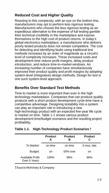
Benefits Over Standard Test MethodsTime to market is more important than ever in the hightechnology marketplace. Companies that can produce qualityproducts with a short product development cycle-time have acompetitive advantage. Designing testability into a systemcan play an important role in introducing a newhigh-technology product with an expected five-year life cycleto market on time. Table 1-1 shows various productdevelopment time/budget scenarios and the resulting projectprofitability.
Table 1-1. High-Technology Product Scenarios�
ProductA
ProductB
ProductC
To Market: on time on time 6 mos. late
Budget: on 50% over on
Available ProfitOver 5 Years:
100% 96% 66%
�Source:McKinsey & Company
1-4 Introduction
Adding testability to a product increases design time andcosts, while reducing costs of design validation,manufacturing test, and system maintenance.
The system design phase of product developmentrepresents only 15 percent of a product’s total life-cycle cost.However, the system design phase has a 70-percent impacton a product’s operation and support costs over the product’stotal life (source: Mitre Corporation, 1987 GovernmentMicrocircuit Applications Conference).
The majority of faults found on boards, such as solder joints(shorts and opens), components (wrong device, missingdevice, wrong orientation, wire-bond failure, and stuck pins),etch integrity, and connector faults, make up over 95 percentof failures found. A structured technique such asboundary-scan testing allows for pins-out testing to easilydetect these failures (source: Teradyne).
The additional cost of designing testability into a systemduring the system design phase can be more than offsetover the product’s total life.
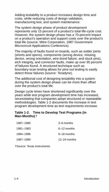
Design cycle times have shortened significantly over theyears while test program development time has increased,necessitating that companies adopt structured or repeatablemethodologies. Table 1-2 documents the increase in testprogram development time as test requirements increase.
Table 1-2. Time to Develop Test Programs (inMan-Months)†
1987–1980 3–6 months
1981–1983 6–12 months
1984–1986 9–18 months
1987–1990 12–24 months
†Source: Texas Instruments

1-5
Standard Test Solutions Versus ProprietarySolutionsEmbedded test, emulation, and maintenance circuitry arewell defined and understood within the test community.Previously, the lack of standards caused these structures tobe implemented in an ad hoc and proprietary manner. Sinceproprietary solutions are usually more expensive and laborintensive, the added costs further limited the use of thesetest circuits. Boundary-scan testing combined with acommon test bus interface and test protocol has thesebenefits:
Provides a standard and cost-effective solution totraditional test problems
Opens new applications
The ability to reuse previously developed test data and touse less costly test equipment means that this approachyields products that are less expensive to manufacture.
An Industry Standard — IEEE Std 1149.1-1990(JTAG)In 1985, an ad hoc group composed of key electronicmanufacturers joined to form the Joint Test Action Group(JTAG). JTAG had over 200 members around the world,including major electronics and semiconductormanufacturers. This group met to establish a solution to theproblems of board test and to promote a solution as anindustry standard. The solution, which became IEEE Std1149.1-1990, IEEE Standard Test Access Port andBoundary-Scan Architecture, is the basis for TexasInstruments (TI ) testability products. IEEE Std 1149.1allows test instructions and data to be serially loaded into adevice and enables the subsequent test results to be seriallyread out.
Every IEEE Std 1149.1-compatible device has four additionalpins — two for control and one each for input and outputserial test data. To be compatible, a component must havecertain basic test features, but IEEE Std 1149.1 allowsdesigners to add test features to meet their own uniquerequirements. The specification was adopted as an IEEEstandard in February 1990.
2-1
Chapter 2Benefits of Testability
This chapter explains how designing testability into deviceseliminates problems associated with traditional testing andimproves quality and efficiency.
Traditional TestingTraditional board-level and device-level testing consumes agreat deal of time and requires special hardware andcomplex automatic test equipment (ATE) for each type ofboard or device. This results in increased costs anddevelopment time. In addition, extensive testing is necessaryfor the evermore stringent reliability standards andperformance standards in the defense, aerospace,automotive, computer, and communications industries.These extensive tests can delay the market introduction ofproducts, disrupt just-in-time (JIT) manufacturing flows, andlimit the productivity of standard ATE operations. Thiscreates numerous problems because time to market is moreimportant than ever in the high-technology marketplace.Companies that produce quality products with a shortproduct-development cycle time have a competitiveadvantage.
Efficient TestingAn innovative approach to the problems inherent withtraditional testing is to incorporate design-for-test techniquesthat allow embedded testing to be performed. For example,data can be scanned in to stimulate internal system nodeswhile the component or circuit is embedded within thesystem. During the same scan, the previous condition ofeach node is scanned out. This saves test time and reducesthe number of test vectors needed.
Lower Cost for TestingThe additional cost of designing testability into a systemduring the design phase is more than offset over theproduct’s total life. This is accomplished by reducing the testprogram development time, minimizing fixture complexity,and allowing for the use of lower-cost ATE solutions. Anothercost benefit is the economy of scale gained by having astandard test approach that spans design, test, manufacture,field repairs, and maintenance.
2-2 Benefits of Testability
Production Time SavingsBoard-level boundary-scan testing is easily implementedusing TI’s line of IEEE Std 1149.1 testability devices, suchas:
Widebus and octal bus interfaces
Scan-support devices
ASIC and DSPThese IEEE Std 1149.1-compliant devices are included inboard design with little modification to existing circuitry.Embedded testability greatly reduces the need for other testpoints on the board, and offers these advantages:
Greatly simplified test fixtures
Reduced fixture construction time
Sophisticated built-in test and debug operationsMany ICs or boards can be tested together using the serialIEEE Std 1149.1 test bus under the control of boundary-scantest software.
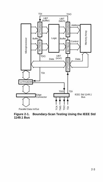
Easier Board-Level IsolationFault isolation on a printed circuit board can be greatlyimproved by electronically isolating suspect areas usingboundary-scannable devices. The IEEE Std 1149.1 test buscontrols boundary-scannable devices to place them inEXTEST for pins-out testing. This effectively partitions orisolates circuitry for separate testing. Partitioning a systemusing IEEE Std 1149.1-compliant devices reduces thenumber of patterns required for testing each circuit area. SeeFigure 2-1 for an example of a design than can bepartitioned.
Simple Access to CircuitsHighly integrated, modern, multilayer systems or lCs withfine-pitch pins are virtually impossible to access usingmanual probes or ATE. Some boards require extensivefixturing or redesign before they can be tested effectively.TI’s testability devices with boundary-scan architectureeliminate physical access problems. These parts provide thedesigner with testability for the most complex andhard-to-access circuits, and add controllability of test circuits.In addition, a designer can easily observe and controlinternal device functions.
2-3
’BC
T82
44
’BC
T82
44
’LVTH18245
’LV
TH
1850
4
’LV
TH
1850
2’A
BT
H18
504
TDI
TDI
TDO
TDO
TDI
TDO
Buffer
DataData
Buffer
Mic
ropr
oces
sor
Mem
ory
Arr
ay
EdgeConnector
Parallel Data In/Out
UBT
UBT
Address
Control
UBT
TC
K
TM
S
TD
O
TD
I
Logic
IEEE Std 1149.1Bus
(latch)(buffer)
(xcvr)
Figure 2-1. Boundary-Scan Testing Using the IEEE Std1149.1 Bus
3-1
Chapter 3Boundary-Scan Architecture
and IEEE Std 1149.1
Boundary scan is a special type of scan path with a registeradded at every I/O pin on a device. Although this requiresthe addition of a special test latch on some pins, thetechnique offers several important benefits. The mostobvious benefit offered by the boundary-scan technique isallowing fault isolation at the component level. Such anisolation requirement is common in telecomunicationsswitching environments where prompt field repair is critical.
A major problem driving the development of IEEE Std 1149.1boundary scan is the adverse effect of surface-mounttechnology. The inclusion of a boundary-scan path insurface-mount components, in many cases, affords the onlyway to perform continuity tests between devices. By placinga known value on an output buffer of one device andobserving the input buffer of another interconnected device, itis easy to see if the printed wiring board (PWB) net iselectrically connected. Failure of this simple test indicatesbroken circuit traces, cold solder joints, solder bridges, orelectrostatic-discharge (ESD) induced failures in an ICbuffer — all common problems on PWBs.
A less-obvious advantage of the boundary-scanmethodology is the ability to apply predeveloped functionalpattern sets to the I/O pins of the IC by way of the scan path.IC manufacturers and ASIC developers create functionalpattern sets for DC test purposes. Subsets of these patternscan be reused for in-circuit functional IC testing. Reusingexisting patterns in the development of system diagnosticscan save large amounts of development resources,especially if many of the ICs in a system have embeddedboundary-scan paths.
IEEE Std 1149.1 is a common protocol and boundary-scanarchitecture developed into an industrial standard afterthousands of man hours of cooperative development byapproximately 200 major international electronics firms. Earlycontributors in the development of IEEE Std 1149.1 wereAT&T, DEC , Ericsson, IBM , Nixdorf, Philips, Siemens,and TI. These companies recognized that only anonproprietary architecture would encourage companies to
3-2 Boundary-Scan Architecture and IEEE Std 1149.1
offer the compatible integrated circuits, test equipment, andCAD software needed to bring product development,manufacturing, and test costs under control in today’scompetitive electronics marketplace. Many people believethat boundary-scan architecture will do for development,manufacturing, and test what the RS-232C standard did forcomputer peripherals.
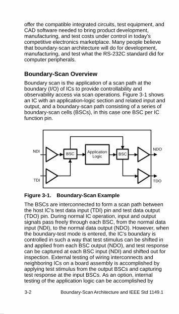
Boundary-Scan OverviewBoundary scan is the application of a scan path at theboundary (I/O) of ICs to provide controllability andobservability access via scan operations. Figure 3-1 showsan IC with an application-logic section and related input andoutput, and a boundary-scan path consisting of a series ofboundary-scan cells (BSCs), in this case one BSC per ICfunction pin.
ApplicationLogic BSC
TDI TDO
NDI NDOBSC
Figure 3-1. Boundary-Scan Example
The BSCs are interconnected to form a scan path betweenthe host IC’s test data input (TDI) pin and test data output(TDO) pin. During normal IC operation, input and outputsignals pass freely through each BSC, from the normal datainput (NDI), to the normal data output (NDO). However, whenthe boundary-test mode is entered, the IC’s boundary iscontrolled in such a way that test stimulus can be shifted inand applied from each BSC output (NDO), and test responsecan be captured at each BSC input (NDI) and shifted out forinspection. External testing of wiring interconnects andneighboring ICs on a board assembly is accomplished byapplying test stimulus from the output BSCs and capturingtest response at the input BSCs. As an option, internaltesting of the application logic can be accomplished by
3-3
applying test stimulus from the input BSCs and capturing testresponse at the output BSCs. The implementation of a scanpath at the boundary of IC designs provides an embeddedtesting capability that can overcome the physical accessproblems in current and future board designs.
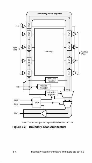
Test Interface and Boundary-Scan ArchitectureFigure 3-2 shows the IEEE Std 1149.1 architecture. Thearchitecture consists of an instruction register, a bypassregister, a boundary-scan register (highlighted), optional userdata register(s), and a test interface referred to as the testaccess port (TAP). In Figure 3-2, the boundary-scan register(BSR), a serially accessed data register made up of a seriesof boundary-scan cells (BSCs), is shown at the input andoutput boundary of the IC.
The instruction register and data registers are separate scanpaths arranged between the primary test data input (TDI) pinand primary test data output (TDO) pin. This architectureallows the TAP to select and shift data through one of the twotypes of scan paths, instruction or data, without accessingthe other scan path.
3-4 Boundary-Scan Architecture and IEEE Std 1149.1
InputPins
OutputPins
TDI
TMS
TCK
TDO
TAP
User DataRegister
BypassResister
InstructionRegister
Note: The boundary-scan register is shifted TDI to TDO.
BS
CB
SC
BS
CB
SC
BS
C
BS
C
BS
C
BS
C
BS
COE
Core Logic
Boundary-Scan Register
Figure 3-2. Boundary-Scan Architecture
3-5
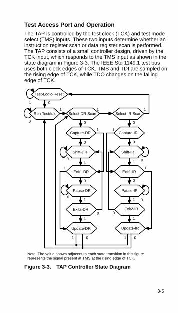
Test Access Port and OperationThe TAP is controlled by the test clock (TCK) and test modeselect (TMS) inputs. These two inputs determine whether aninstruction register scan or data register scan is performed.The TAP consists of a small controller design, driven by theTCK input, which responds to the TMS input as shown in thestate diagram in Figure 3-3. The IEEE Std 1149.1 test bususes both clock edges of TCK. TMS and TDI are sampled onthe rising edge of TCK, while TDO changes on the fallingedge of TCK.
Shift-DR
1 0
1
0
1 1
0
0
1
0
0
1
1 0 0
0
0
1
0
0
1
1
1 1
0
0
0
0
1 1
1 1
Note: The value shown adjacent to each state transition in this figure represents the signal present at TMS at the rising edge of TCK.
Pause-DR
Update-DR
Test-Logic-Reset
Capture-DR Capture-IR
Shift-IR
Exit1-DR Exit1-IR
Pause-IR
Exit2-DR Exit2-IR
Update-IR
Select-DR-Scan Select-IR-ScanRun-Test/Idle
Figure 3-3. TAP Controller State Diagram
3-6 Boundary-Scan Architecture and IEEE Std 1149.1
The main state diagram consists of six steady states:Test-Logic-Reset, Run-Test/Idle, Shift-DR, Pause-DR,Shift-IR, and Pause-IR. A unique feature of this protocol isthat only one steady state exists for the condition when TMSis set high: the Test-Logic-Reset state. This means that areset of the test logic can be achieved within five TCKs orless by setting the TMS input high.
At power up, or during normal operation of the host IC, theTAP is forced into the Test-Logic-Reset state by driving TMShigh and applying five or more TCKs. In this state, the TAPissues a reset signal that places all test logic in a conditionthat does not impede normal operation of the host IC. Whentest access is required, a protocol is applied via the TMS andTCK inputs, causing the TAP to exit the Test-Logic-Resetstate and move through the appropriate states. From theRun-Test/Idle state, an instruction register scan or a dataregister scan can be issued to transition the TAP through theappropriate states shown in Figure 3-3.
The states of the data register scan and instruction registerscan blocks are mirror images of each other, addingsymmetry to the protocol sequences. The first action thatoccurs when either block is entered is a capture operation.For the data registers, the Capture-DR state is used tocapture (or parallel load) the data into the selected serialdata path. If the BSR is the selected data register, the normaldata inputs (NDIs) are captured during this state. In theinstruction register, the Capture-IR state is used to capturestatus information into the instruction register.
From the Capture state, the TAP transitions to either the Shiftor Exit1 state. Normally, the Shift state follows the Capturestate so that test data or status information can be shifted outfor inspection and new data shifted in. Following the Shiftstate, the TAP either returns to the Run-Test/Idle state via theExit1 and Update states or enters the Pause state via Exit1.The reason for entering the Pause state is to temporarilysuspend the shifting of data through either the selected dataregister or instruction register while a required operation,such as refilling a tester memory buffer, is performed. Fromthe Pause state, shifting can resume by re-entering the Shiftstate via the Exit2 state or be terminated by entering theRun-Test/Idle state via the Exit2 and Update states.
3-7
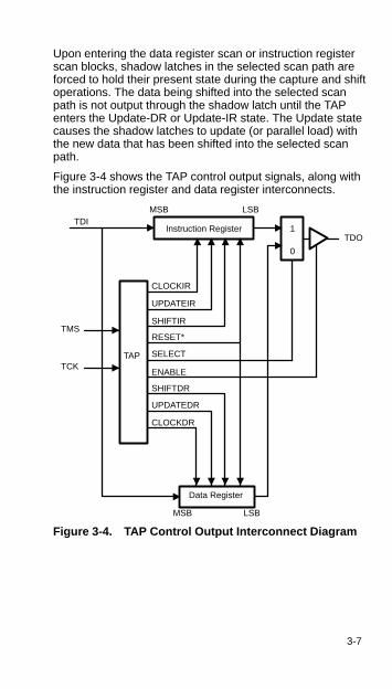
Upon entering the data register scan or instruction registerscan blocks, shadow latches in the selected scan path areforced to hold their present state during the capture and shiftoperations. The data being shifted into the selected scanpath is not output through the shadow latch until the TAPenters the Update-DR or Update-IR state. The Update statecauses the shadow latches to update (or parallel load) withthe new data that has been shifted into the selected scanpath.
Figure 3-4 shows the TAP control output signals, along withthe instruction register and data register interconnects.
Instruction Register
Data Register
TAP
TDI
TMS
TCK
MSB LSB
MSB LSB
TDO
CLOCKIR
UPDATEIR
SHIFTIR
RESET*
SELECT
ENABLE
SHIFTDR
UPDATEDR
CLOCKDR
1
0
Figure 3-4. TAP Control Output Interconnect Diagram
3-8 Boundary-Scan Architecture and IEEE Std 1149.1
IEEE Std 1149.1 RegistersThis section contains descriptions of the required andoptional registers specified in IEEE Std 1149.1-1990.
Instruction Register (Required)
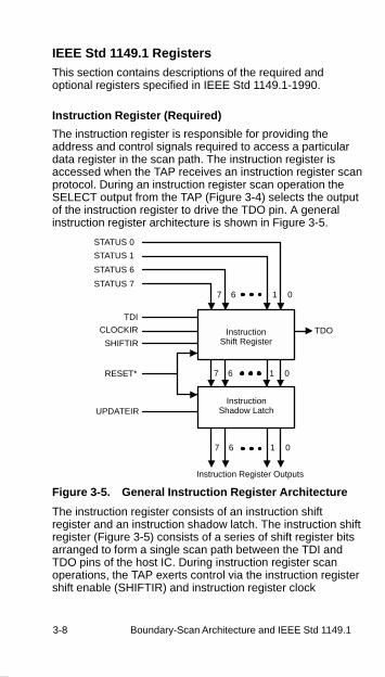
The instruction register is responsible for providing theaddress and control signals required to access a particulardata register in the scan path. The instruction register isaccessed when the TAP receives an instruction register scanprotocol. During an instruction register scan operation theSELECT output from the TAP (Figure 3-4) selects the outputof the instruction register to drive the TDO pin. A generalinstruction register architecture is shown in Figure 3-5.
TDOInstructionShift Register
InstructionShadow Latch
STATUS 1
STATUS 6
STATUS 7
TDI
CLOCKIR
SHIFTIR
RESET*
UPDATEIR
7 6 1 0
Instruction Register Outputs
7 6 1 0
7 6 1 0
STATUS 0
Figure 3-5. General Instruction Register Architecture
The instruction register consists of an instruction shiftregister and an instruction shadow latch. The instruction shiftregister (Figure 3-5) consists of a series of shift register bitsarranged to form a single scan path between the TDI andTDO pins of the host IC. During instruction register scanoperations, the TAP exerts control via the instruction registershift enable (SHIFTIR) and instruction register clock
3-9
(CLOCKIR) signals to cause the instruction shift register topreload status information and shift data from TDI to TDO.Both the preload and shift operations occur on the risingedge of TCK; however, the data shifted out from the host ICfrom TDO occurs on the falling edge of TCK. The statusinputs are user-defined observability inputs, except for thetwo least-significant bits, which are always 01 for scan-pathtesting purposes. (The instruction register has a minimumlength of two bits.)
The instruction shadow register (Figure 3-5) consists of aseries of latches, one latch for each instruction shift registerbit. During an instruction register scan operation, the latchesremain in their present state. At the end of the instructionregister scan operation, the instruction register update(UPDATEIR) input updates the latches with the newinstruction installed in the instruction shift register. Whenactivated, the RESET* input sets the instruction shadowregister to the value of the BYPASS instruction (or IDCODEinstruction, if it is supported). This forces the device into itsnormal functional mode and selects the bypass register (ordevice identification register, if one is present).
Data Registers
IEEE Std 1149.1 requires two data registers; boundary-scanregister and bypass register, with a third, optional, deviceidentification register. Additional user-defined data registerscan be included. The data registers are arranged in parallelfrom the primary TDI input to the primary TDO output. Theinstruction register supplies the address that allows one ofthe data registers to be accessed during a data register scanoperation. During a data register scan operation, theaddressed scan register receives TAP control via the dataregister shift enable (SHIFTDR) and data register clock(CLOCKDR) inputs to preload test response and shift datafrom TDI to TDO. During a data register scan operation, theSELECT output from the TAP (Figure 3-4) selects the outputof the data register to drive the TDO pin. When one scanpath in the data register is being accessed, all other scanpaths remain in their present state.
3-10 Boundary-Scan Architecture and IEEE Std 1149.1
Boundary-Scan Register
Bypass Register
TDO
Device Identification Register
Design-Specific Test Data Register
Design-Specific Test Data Register
Design-Specific Test Data Register
FromTDI
To
Clock and Control Signals From InstructionRegister, TAP Controller, etc.
Optional
Optional
Optional
Optional
MUX
G
MUX
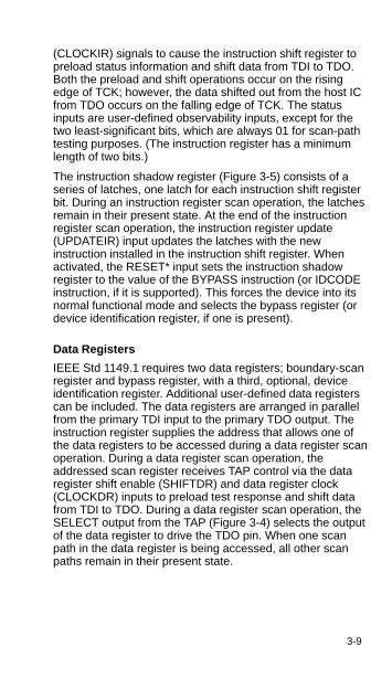
Figure 3-6. Test Data Register Architecture
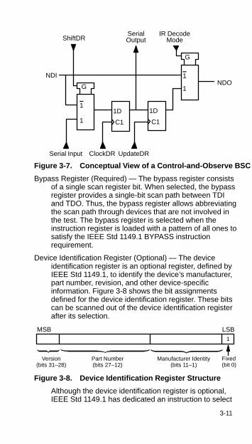
Boundary-Scan Register — The boundary-scan register(BSR) consists of a series of boundary-scan cells(BSCs) arranged to form a scan path around theboundary of the host IC. The BSCs provide thecontrollability and observability features required toperform boundary-scan testing as described in theBoundary-Scan Overview section of this chapter.Shadow latches in the BSCs, driving the NDO outputsremain in their present state during a data register scanoperation. At the end of a data register scan operation,the data register update (UPDATEDR) input updatesthe shadow latches with the new boundary test patternto be applied from the NDO outputs of the BSCs.Figure 3-7 shows a conceptual view of acontrol-and-observe BSC.
3-11
1D
C1
NDO
ShiftDR
NDI
Serial Input
Serial IR Decode
ClockDR UpdateDR
Output Mode
G
G
1
1
1D
C1
1
1
Figure 3-7. Conceptual View of a Control-and-Observe BSC
Bypass Register (Required) — The bypass register consistsof a single scan register bit. When selected, the bypassregister provides a single-bit scan path between TDIand TDO. Thus, the bypass register allows abbreviatingthe scan path through devices that are not involved inthe test. The bypass register is selected when theinstruction register is loaded with a pattern of all ones tosatisfy the IEEE Std 1149.1 BYPASS instructionrequirement.
Device Identification Register (Optional) — The deviceidentification register is an optional register, defined byIEEE Std 1149.1, to identify the device’s manufacturer,part number, revision, and other device-specificinformation. Figure 3-8 shows the bit assignmentsdefined for the device identification register. These bitscan be scanned out of the device identification registerafter its selection.
MSB LSB
Version(bits 31–28)
Part Number(bits 27–12)
Manufacturer Identity(bits 11–1)
1
Fixed(bit 0)
Figure 3-8. Device Identification Register Structure
Although the device identification register is optional,IEEE Std 1149.1 has dedicated an instruction to select
3-12 Boundary-Scan Architecture and IEEE Std 1149.1
this register. The device identification register isselected when the instruction register is loaded with theIDCODE instruction, the bit code of which is defined bythe vendor.
Manufacturer’s identity codes (bit1 through bit11) areassigned, maintained, and updated by the EIA/JEDECoffice. Any company can be added to the JEDECStandard Manufacturer’s Identification Code(Publication JEP106) by request to the JEDEC office at202-457-4973.
IEEE Std 1149.1 Required InstructionsIEEE Std 1149.1 defines nine test instructions. Of the nineinstructions, three are required and six are optional. Thefollowing subsections contain brief descriptions of eachrequired test instruction.
BYPASS Instruction
The required BYPASS instruction allows the IC to remain in afunctional mode and selects the bypass register to beconnected between TDI and TDO. The BYPASS instructionallows serial data to be transferred through the IC from TDIto TDO without affecting the operation of the IC. The bit codeof this instruction is defined as all ones by IEEE Std 1149.1.
SAMPLE/PRELOAD Instruction
The required SAMPLE/PRELOAD instruction allows the IC toremain in its functional mode and selects the boundary-scanregister to be connected between TDI and TDO. During thisinstruction, the boundary-scan register can be accessed viaa data scan operation, to take a sample of the functional dataentering and leaving the IC. This instruction is also used topreload test data into the boundary-scan register beforeloading an EXTEST instruction. The bit code for thisinstruction is defined by the vendor.
3-13
EXTEST Instruction
The required EXTEST instruction places the IC into anexternal boundary-test mode and selects the boundary-scanregister to be connected between TDI and TDO. During thisinstruction, the boundary-scan register is accessed to drivetest data off-chip via the boundary outputs and receive testdata off-chip via the boundary inputs. The bit code of thisinstruction is defined as all zeroes by IEEE Std 1149.1.
IEEE Std 1149.1 Optional InstructionsThe following subsections contain brief descriptions of theoptional IEEE Std 1149.1 instructions.
INTEST Instruction
The optional INTEST instruction places the IC in an internalboundary-test mode and selects the boundary-scan registerto be connected between TDI and TDO. During thisinstruction, the boundary-scan register is accessed to drivetest data on-chip via the boundary inputs and receive testdata on-chip via the boundary outputs. The bit code of thisinstruction is defined by the vendor.
RUNBIST Instruction
The optional RUNBIST instruction places the IC in a self-testmode, enables a comprehensive self-test of the IC’s corelogic, and selects a user-specified data register to beconnected between TDI and TDO. During this instruction, theboundary outputs are controlled so that they cannot interferewith neighboring ICs during the RUNBIST operation. Also,the boundary inputs are controlled so that external signalscannot interfere with the RUNBIST operation. The bit code ofthis instruction is defined by the vendor.
CLAMP Instruction
The optional CLAMP instruction sets the outputs of an IC tologic levels determined by the contents of the boundary-scanregister and selects the bypass register to be connectedbetween TDI and TDO. Before loading this instruction, thecontents of the boundary-scan register can be preset withthe SAMPLE/PRELOAD instruction. During this instruction,data can be shifted through the bypass register from TDI to
3-14 Boundary-Scan Architecture and IEEE Std 1149.1
TDO without affecting the condition of the outputs. The bitcode of this instruction is defined by the vendor.
HIGHZ Instruction
The optional HIGHZ instruction sets all outputs (includingtwo-state as well as three-state types) of an IC to a disabled(high-impedance) state and selects the bypass register to beconnected between TDI and TDO. During this instruction,data can be shifted through the bypass register from TDI toTDO without affecting the condition of the IC outputs. The bitcode of this instruction is defined by the vendor.
IDCODE Instruction
The optional IDCODE instruction allows the IC to remain inits functional mode and selects the optional deviceidentification register to be connected between TDI andTDO. The device identification register (see Figure 3-8) is a32-bit shift register containing information regarding the ICmanufacturer, device type, and version code. Accessing thedevice identification register does not interfere with theoperation of the IC. Also, access to the device identificationregister should be immediately available, via a TAPdata-scan operation, after power-up of the IC or after theTAP has been reset using the optional TRST* pin or byotherwise moving to the Test-Logic-Reset state. The bit codeof this instruction is defined by the vendor.
USERCODE Instruction
The optional USERCODE instruction allows the IC to remainin its functional mode and selects the device identificationregister to be connected between TDI and TDO. During theUSERCODE instuction, the optional 32-bit deviceidentification register captures user-defined informationabout the IC. Accessing the device identification registerdoes not interfere with the operation of the IC. The bit codeof this instruction is defined by the vendor.
3-15
Obtaining IEEE Std 1149.1-1990To learn more about IEEE Std 1149.1, please refer to thepublications, IEEE Standard Test Access Port andBoundary-Scan Architecture, IEEE Std 1149.1-1990(includes IEEE Std 1149.1a-1993) and Supplement to IEEEStd 1149.1-1990, IEEE Standard Test Access Port andBoundary-Scan Architecture, IEEE Std 1149.1b-1994. Thesedocuments are available through IEEE (1-800-678-IEEE).IEEE Std 1149.1-1990/IEEE Std 1149.1a-1993 is alsoavailable from Texas Instruments on CD-ROM (seeChapter 9, Other Support and Learning Products).
4-1
Chapter 4Using DFT in ASICs
The concern most often voiced by application-specificintegrated circuit (ASIC) users is that of testability. Thischapter is intended to provide an understanding of ASICtestability that can be used for developing test strategieswhen designs are being initiated.
Design-for-Test ConsiderationsDesigning testability into any circuit affects the hardware tosome degree. Additional logic will probably have to beadded. This additional logic increases the amount of siliconrequired to implement the design. The savings fromenhanced testability do not usually show up until the cycletime and testing cost of the circuit and its end system areanalyzed.
Fault simulation is an important part of designing fortestability. This technique enables you to evaluate your testpatterns to determine whether these patterns detect faults.Faults may occur during either the design-tooling stage orthe circuit-fabrication stage. A fault simulator uses faultmodels, such as a node shorted to power (stuck-at-one) or anode shorted to ground (stuck-at-zero), and compares theresponse of a fault-free circuit with the response of a faultycircuit. If the response of the fault-free circuit is different thanthe response of the faulty circuit, then the test patterns havedetected the fault.
By faulting all the nodes in the circuit, the fault simulatorproduces the test-pattern fault grade or fault coverage. Thefault coverage is the percentage of faults detected amongthe total faults. The higher the fault coverage, the better thetest pattern set separates a faulty circuit from a fault-freecircuit. After determining which faults have not been detectedby the current set of test patterns, additional test patternscan be generated to detect those faults.
Adoption of design-for-test principles early in the designprocess ensures the maximum testability for the minimumeffort. These guidelines emphasize that test is a part of thedesign flow, not a process that is done at the end of thedesign cycle.
4-2 Using DFT in ASICs
Three basic elements must come together to make asuccessful ASIC circuit:
Logic design, including schematic capture, libraryselection, synthesis, and simulation
Logic testability, including fault-detection andtest-application criteria within predefined cost andtime-scale budgets
Vendor’s manufacturing capability, including processingand packaging
The Need for TestabilityMost engineers involved in the design of ASIC devices arefamiliar with the trade-offs between gate arrays, standardcells, and full custom devices. They are also familiar with thevendor selection process. The aspect of test capability andtestability is often overlooked.
Testability could be ignored when typical designs were only afew thousand gates. These designs were implemented firstand then turned over to a test engineer or to a vendor tocreate a test program for production. As design complexitiesincreased, this approach to testing became futile. Successfulhigh-density ASIC design and manufacturing demand thatcircuits be built with testability incorporated into the designprocess.
Although testability imposes additional constraints in thedesign phase, design verification and test can beunmanageable, if ignored until the design is completed andtestability is handled as a postdesign insertion. In fact, thedesign constraints are overwhelmingly balanced by improvedtestability, which adds value to the device throughoutmanufacturing and system life.
4-3
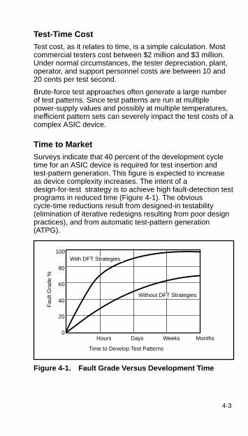
Test-Time CostTest cost, as it relates to time, is a simple calculation. Mostcommercial testers cost between $2 million and $3 million.Under normal circumstances, the tester depreciation, plant,operator, and support personnel costs are between 10 and20 cents per test second.
Brute-force test approaches often generate a large numberof test patterns. Since test patterns are run at multiplepower-supply values and possibly at multiple temperatures,inefficient pattern sets can severely impact the test costs of acomplex ASIC device.
Time to MarketSurveys indicate that 40 percent of the development cycletime for an ASIC device is required for test insertion andtest-pattern generation. This figure is expected to increaseas device complexity increases. The intent of adesign-for-test strategy is to achieve high fault-detection testprograms in reduced time (Figure 4-1). The obviouscycle-time reductions result from designed-in testability(elimination of iterative redesigns resulting from poor designpractices), and from automatic test-pattern generation(ATPG).
Hours Days Weeks Months
Time to Develop Test Patterns
Fau
lt G
rade
%
With DFT Strategies
Without DFT Strategies
100
80
60
40
20
0
Figure 4-1. Fault Grade Versus Development Time
4-4 Using DFT in ASICs
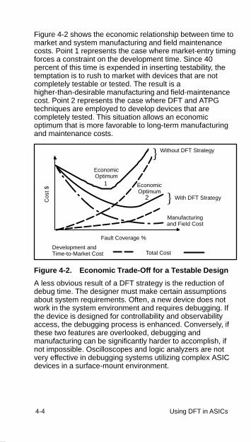
Figure 4-2 shows the economic relationship between time tomarket and system manufacturing and field maintenancecosts. Point 1 represents the case where market-entry timingforces a constraint on the development time. Since 40percent of this time is expended in inserting testability, thetemptation is to rush to market with devices that are notcompletely testable or tested. The result is ahigher-than-desirable manufacturing and field-maintenancecost. Point 2 represents the case where DFT and ATPGtechniques are employed to develop devices that arecompletely tested. This situation allows an economicoptimum that is more favorable to long-term manufacturingand maintenance costs.
EconomicOptimum
EconomicOptimum
Without DFT Strategy
With DFT Strategy
Manufacturingand Field Cost
Development andTime-to-Market Cost Total Cost
Fault Coverage %
Cos
t $
�
�
1
2
Figure 4-2. Economic Trade-Off for a Testable Design
A less obvious result of a DFT strategy is the reduction ofdebug time. The designer must make certain assumptionsabout system requirements. Often, a new device does notwork in the system environment and requires debugging. Ifthe device is designed for controllability and observabilityaccess, the debugging process is enhanced. Conversely, ifthese two features are overlooked, debugging andmanufacturing can be significantly harder to accomplish, ifnot impossible. Oscilloscopes and logic analyzers are notvery effective in debugging systems utilizing complex ASICdevices in a surface-mount environment.
4-5
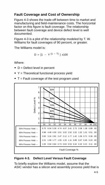
Fault Coverage and Cost of OwnershipFigure 4-3 shows the trade-off between time to market andmanufacturing and field-maintenance costs. The horizontalfactor on this figure is fault coverage. The relationshipbetween fault coverage and device defect level is welldocumented.
Figure 4-3 is a plot of the relationship modeled by T. W.Williams for fault coverages of 90 percent, or greater.
The Williams model is:
D� [1 � Y (1� T) ] x100
Where:
D = Defect level in percent
Y = Theoretical functional process yield
T = Fault coverage of the test program used
7
6
5
4
3
2
1
0
50%
60%
70%
80%
90%
Def
ect L
evel
%
Fault Coverage %
90
6.70
4.98
3.50
2.21
1.05
91
6.04
4.48
3.16
1.99
0.94
92
5.39
4.00
2.81
1.77
0.84
93
4.74
3.51
2.47
1.55
0.73
94
4.07
3.02
2.12
1.33
0.63
95
3.41
2.52
1.77
1.11
0.53
96
2.73
2.02
1.42
0.89
0.42
97
2.08
1.52
1.06
0.67
0.32
98
1.38
1.01
0.71
0.45
0.21
99
0.89
0.51
0.36
0.22
0.11
100
.00
.00
.00
.00
.00
50% Process Yield —
60% Process Yield —
70% Process Yield —
80% Process Yield —
90% Process Yield —
Figure 4-3. Defect Level Versus Fault Coverage
To briefly explore the Williams model, assume that theASIC vendor has a silicon and assembly process yield that is
4-6 Using DFT in ASICs
70 percent. If the fault grade of the test program is also 70percent, the defect level is projected to be 10.1 percent, or101,000 ppm (this is outside the limits of the chart and wascalculated). At a fault grade of 90 percent, the defect level isprojected to be 3.5 percent or 35,000 ppm.
A study of the model shows that the process yield becomesan insignificant term when the fault coverage of the testprogram is very close to 100 percent.
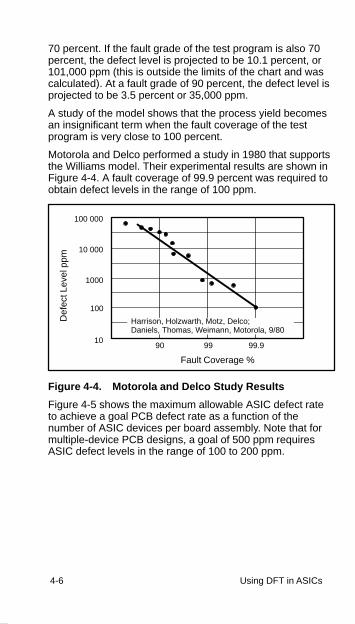
Motorola and Delco performed a study in 1980 that supportsthe Williams model. Their experimental results are shown inFigure 4-4. A fault coverage of 99.9 percent was required toobtain defect levels in the range of 100 ppm.
Fault Coverage %
Def
ect L
evel
ppm
90 99 99.9
10 000
1000
100
10
Harrison, Holzwarth, Motz, Delco;Daniels, Thomas, Weimann, Motorola, 9/80
100 000
Figure 4-4. Motorola and Delco Study Results
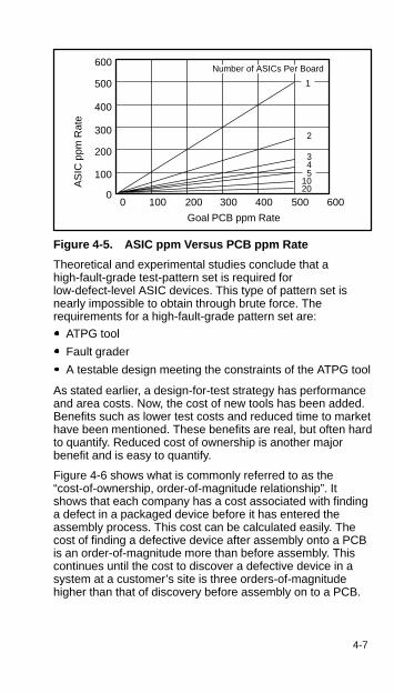
Figure 4-5 shows the maximum allowable ASIC defect rateto achieve a goal PCB defect rate as a function of thenumber of ASIC devices per board assembly. Note that formultiple-device PCB designs, a goal of 500 ppm requiresASIC defect levels in the range of 100 to 200 ppm.
4-7
Goal PCB ppm Rate
AS
IC p
pm R
ate
0
300
200
100
0
400
500
100 200 300 400 500 600
1
2
34
20
600Number of ASICs Per Board
510
Figure 4-5. ASIC ppm Versus PCB ppm Rate
Theoretical and experimental studies conclude that ahigh-fault-grade test-pattern set is required forlow-defect-level ASIC devices. This type of pattern set isnearly impossible to obtain through brute force. Therequirements for a high-fault-grade pattern set are:
ATPG tool
Fault grader
A testable design meeting the constraints of the ATPG tool
As stated earlier, a design-for-test strategy has performanceand area costs. Now, the cost of new tools has been added.Benefits such as lower test costs and reduced time to markethave been mentioned. These benefits are real, but often hardto quantify. Reduced cost of ownership is another majorbenefit and is easy to quantify.
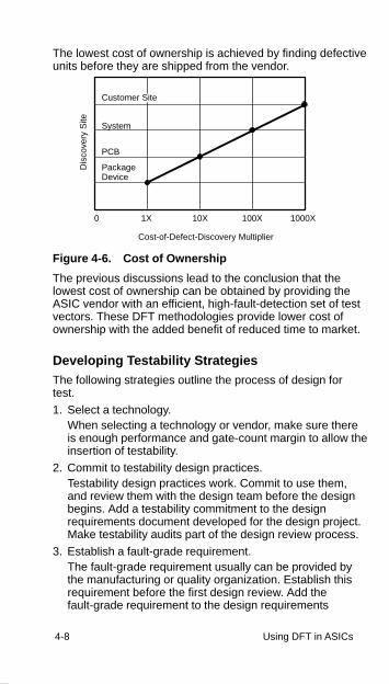
Figure 4-6 shows what is commonly referred to as the“cost-of-ownership, order-of-magnitude relationship”. Itshows that each company has a cost associated with findinga defect in a packaged device before it has entered theassembly process. This cost can be calculated easily. Thecost of finding a defective device after assembly onto a PCBis an order-of-magnitude more than before assembly. Thiscontinues until the cost to discover a defective device in asystem at a customer’s site is three orders-of-magnitudehigher than that of discovery before assembly on to a PCB.
4-8 Using DFT in ASICs
The lowest cost of ownership is achieved by finding defectiveunits before they are shipped from the vendor.
0
Cost-of-Defect-Discovery Multiplier
Dis
cove
ry S
ite
1X 10X 100X 1000X
Customer Site
System
PCB
PackageDevice
Figure 4-6. Cost of Ownership
The previous discussions lead to the conclusion that thelowest cost of ownership can be obtained by providing theASIC vendor with an efficient, high-fault-detection set of testvectors. These DFT methodologies provide lower cost ofownership with the added benefit of reduced time to market.
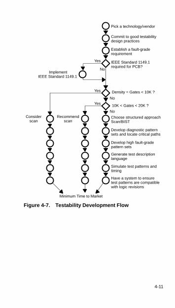
Developing Testability StrategiesThe following strategies outline the process of design fortest.
1. Select a technology.When selecting a technology or vendor, make sure thereis enough performance and gate-count margin to allow theinsertion of testability.
2. Commit to testability design practices.Testability design practices work. Commit to use them,and review them with the design team before the designbegins. Add a testability commitment to the designrequirements document developed for the design project.Make testability audits part of the design review process.
3. Establish a fault-grade requirement.The fault-grade requirement usually can be provided bythe manufacturing or quality organization. Establish thisrequirement before the first design review. Add thefault-grade requirement to the design requirements
4-9
document. This requirement drives many of the decisionsthat follow in the development of the test strategy.Many companies consider the fault-grade requirement tobe an index of device cost of ownership. Failure toachieve it impacts profits throughout the lifetime of thedevice.
4. Decide if IEEE Std 1149.1 is a system requirement.When implemented in an ASIC device, IEEE Std 1149.1allows test of the interconnect between devices on a PCBthrough a four-pin test bus. If IEEE Std 1149.1 is selected,the four dedicated test pins also can be used to controlcore-logic test techniques such as built-in self-test (BIST),internal scan, on-chip emulation, and boundary-scanthrough the test access port (TAP) and instruction register.
5. Select an ASIC testability approach based on gatedensity.
Designs with fewer than 10K gatesDesigns with fewer than 10K gates are not generallycomplex enough to require structured test approaches.The overhead impact is usually too high to justify them.Nonstructured, good design practices are usuallysufficient.
Designs with more than 10K gates, but fewer than 20KgatesStructured techniques should be considered for designsin this density. Nonstructured, good design practices areprobably sufficient for highly combinatorial circuitswithout memory. Structured approaches should beconsidered as complexity is increased by the addition ofsequential circuits, feedback, and memory. Considerboundary-scan testing for reduced cycle times and highfault grades.
Designs with more than 20K gatesThe complexity of circuits this dense usually requiresstructured approaches to achieve high fault grades. Atthis density, it is often hard to control or observe deeply embedded circuits. The overhead associated withstructured testability approaches is acceptable at thisdensity.
4-10 Using DFT in ASICs
6. Choose structured tools.Scan testing is typically the preferred structured approachfor sequential logic. The available scan choices are:
Clocked scan
Multiplexed flip-flop scan
Level-sensitive scan-design (LSSD)
Parallel scan chains
Partial scan
7. Establish a diagnostic functional-pattern set to expeditedebug.This is an important step in decreasing the time to marketfor an ASIC device. The purpose of this pattern set is toisolate circuitry for analysis.
8. Generate high fault-grade test patterns.The fault grade of a test pattern set determines the bestpossible quality level attainable with that set of patterns.
9. Simulate test patterns and timing.Two types of simulation are required during development.Logic simulation verifies both functionality andperformance of the device. Test-pattern simulationproduces the information needed to verify the testpatterns in a tester environment.
Figure 4-7 contains a flow chart that steps through thedesign-for-test process.
4-11
Yes
Yes
Yes
No
No
No
Implement IEEE Standard 1149.1
Considerscan
Recommendscan
Minimum Time to Market
Pick a technology/vendor
Commit to good testabilitydesign practices
Establish a fault-grade requirement
IEEE Standard 1149.1required for PCB?
Density = Gates < 10K ?
10K < Gates < 20K ?
Choose structured approachScan/BIST
Develop diagnostic patternsets and locate critical paths
Develop high fault-gradepattern sets
Simulate test patterns andtiming
Generate test description language
Have a system to ensuretest patterns are compatiblewith logic revisions
Figure 4-7. Testability Development Flow
5-1
Chapter 5Data Formats
Several data formats have emerged to make IEEE Std1149.1 successful and well supported by tools. This chapterdiscusses the most widely accepted data formats thatsupport IEEE Std 1149.1 — BSDL, HSDL, and SVF.
Boundary-Scan Description Language (BSDL)
In 1990, IEEE Std 1149.1 was approved and implementationof the standard accelerated. As more people became awareof and used the standard, the need for a standard method fordescribing IEEE Std 1149.1-compatible devices wasrecognized. The IEEE Std 1149.1 working group establisheda subcommittee to develop a device description language toaddress this need.
The subcommittee has since developed an industry standardlanguage called Boundary-Scan Description Language(BSDL). BSDL is a subset and standard practice of VHDL(VHSIC Hardware Description Language) that describes howIEEE Std 1149.1 is implemented in a device and how itoperates. BSDL captures the essential features of any IEEEStd 1149.1 implementation. BSDL has been formally adoptedas part of IEEE Std 1149.1b-1994.
IEEE Std 1149.1 is a structured design-for-test approach wellsuited for tools and automation. Tools developed to supportthe standard can control the test access port (TAP). If theyknow how the boundary-scan architecture was implementedin the device, such tools can also control the I/O of thedevice. BSDL provides a standard machine- andhuman-readable data format for describing how IEEE Std1149.1 boundary-scan architecture is implemented in adevice.
How BSDL Is Used
Many IEEE Std 1149.1 tools already on the market supportBSDL as a data input format. These tools offer differentcapabilities to customers implementing IEEE Std 1149.1 intotheir designs, including board interconnect automatictest-pattern generation (ATPG) and automatic test equipment(ATE).
5-2 Data Formats
When tools that support BSDL are used, such BSDL is oftenreceived from the semiconductor vendor. This can result insignificant time and cost savings.
Teradyne estimates that to create in-circuit test patterns for aleading microprocessor normally can take as long as sevenweeks:
One week to study the device
Four weeks to develop in-circuit test patterns
Two weeks to verify the patterns on ATE
The development cost estimate for this approach is $14,000.
If the microprocessor supports IEEE Std 1149.1, and theBSDL is supplied by the vendor, the time to develop in-circuittest patterns is less than two hours (less than $100) usingtoday’s tools.
Elements of BSDL
A BSDL description for a device consists of the followingelements:
Entity descriptions
Generic parameter
Logical port description
Use statement(s)
Component conformance statement
Pin mapping(s)
Scan port identification
Instruction register description
Optional register decription
Register access description
Boundary register description
Entity Descriptions — The entity statement names the entity,such as the device name (e.g., SN74BCT8245A). Anentity description begins with an entity statement andterminates with an end statement.entity XYZ is{statements to describe the entity go here}
end XYZ;
5-3
Generic Parameter — A generic parameter is a parameterthat can come from outside the entity, or it can bedefaulted, such as a package type (e.g., “DW”).generic (PHYSICAL_PIN_MAP : string := “DW”);
Logical Port Description — The port description gives logicalnames to the I/O pins (system and TAP pins), anddenotes their nature, such as input, output, bidirectional,linkage (analog or power supply/return) and so on.port (OE:in bit;Y:out bit_vector(1 to 3);A:in bit_vector(1 to 3);GND, VCC, NC:linkage bit;TDO:out bit;TMS, TDI, TCK:in bit);
Use Statement(s) — The use statement refers to externaldefinitions found in packages and package bodies.use STD_1149_1_1994.all;
Component Conformance Statement — The componentconformance statement indicates the latest issue ofIEEE Std 1149.1 to which the device conforms.attribute COMPONENT_CONFORMANCE of XYZ : entity is
“STD_1149_1_1993”;
Pin Mapping(s) — The pin mapping provides a mapping oflogical signals onto the physical pins of a particulardevice package.attribute PIN_MAP of XYZ : entity isPHYSICAL_PIN_MAP;constant DW:PIN_MAP_STRING:=“OE:1, Y:(2,3,4), A:(5,6,7), GND:8, VCC:9, ” &
”TDO:10, TDI:11, TMS:12, TCK:13, NC:14”;
Scan Port Identification — The scan port identificationstatements define the device’s TAP.attribute TAP_SCAN_IN of TDI : signal is TRUE;attribute TAP_SCAN_OUT of TDO : signal is TRUE;attribute TAP_SCAN_MODE of TMS : signal is TRUE;attribute TAP_SCAN_CLOCK of TCK : signal is (50.0e6,
BOTH);
Instruction Register Description — The instruction registerdescription identifies the device-dependentcharacteristics of the instruction register.attribute INSTRUCTION_LENGTH of XYZ : entity is 2;attribute INSTRUCTION_OPCODE of XYZ : entity is“BYPASS (11),”&“EXTEST (00),”&“SAMPLE (10),”&“IDCODE (01)”
attribute INSTRUCTION_CAPTURE of XYZ : entity is “01”;
5-4 Data Formats
Optonal Register Description — The optional registerdescription identifies the values captured in the deviceidentification register for the optional IDCODE andUSERCODE instructions, if supported.attribute IDCODE_REGISTER of XYZ : entity is“01010100000011111100000000101111”;
Register Access Description — The register accessdescription defines which register is placed betweenTDI and TDO for each instruction.attribute REGISTER_ACCESS of XYZ : entity is“BOUNDARY (EXTEST, SAMPLE),”&“BYPASS (BYPASS)”;
Boundary Register Description — The boundary registerdescription contains a list of boundary-scan cells, alongwith information regarding the cell type and associatedcontrol.attribute BOUNDARY_LENGTH of XYZ : entity is 7;attribute BOUNDARY_REGISTER of XYZ : entity is“0 (BC_1, Y(1), output3, X, 6, 0, Z),”&“1 (BC_1, Y(2), output3, X, 6, 0, Z),”&“2 (BC_1, Y(3), output3, X, 6, 0, Z),”&“3 (BC_1, A(1), input , X),”&“4 (BC_1, A(2), input , X),”&“5 (BC_1, A(3), input , X),”&“6 (BC_1, OE , input , X),”&“6 (BC_1, * , control, 0)”;
Verifying BSDL Accuracy
Creating a BSDL file that is syntactically and semanticallycorrect is only the beginning. A syntactically and semanticallycorrect BSDL file can still contain descriptive errors andresult in time-consuming debugging of board-level tests anddiagnostics. A BSDL file must be validated (compared)against the silicon.

5-5
Potential BSDL Errors
As with any hand-entered data, typographical errorspotentially exist. BSDL contains many commas andsemicolons that contribute error possibilities. Fortunately,syntax and semantics errors can easily be identified andcorrected using syntax and semantics checking tools duringthe authoring process.
Other common errors are:Wrong pinout
Wrong cell types
Wrong boundary-scan register order
Wrong boundary-scan register length
Wrong instruction register opcodes
Wrong control cell locations
Wrong control cell disable value
Wrong I/O pin control cell
Wrong identification code value
Wrong capture-IR value
Typographical errors or device documentation errors canresult in implementation errors.
How to Receive the BSDL Specification
Contact the IEEE (1-800-678-IEEE) and refer to Supplementto IEEE Std 1149.1-1990, IEEE Standard Test Access Portand Boundary-Scan Architecture, IEEE Std 1149.1b-1994 toreceive a copy of the Boundary-Scan Description Language(BSDL) specification.
Obtaining BSDL for TI Devices
Texas Instruments makes catalog-device BSDL filesavailable to customers through the World-Wide Web. As ofthis writing, these files can be located on the TexasInstruments IEEE Std 1149.1/JTAG/Boundary-Scan SiliconProducts page located at URL http://www.ti.com/sc/docs/jtag/silicon.htm; or, on the main Texas Instruments homepage at URL http://www.ti.com. Search for keyword BSDL.
5-6 Data Formats
Hierarchical Scan Description Language (HSDL)
Texas Instruments developed the hierarchical scandescription language (HSDL) to complement BSDL, usingthe same subset of VHDL statements as BSDL. HSDL picksup where BSDL stops to describe additional attributes ofIEEE Std 1149.1 devices and how IEEE Std 1149.1 devicesare connected at the board and system levels.
HSDL uses the BSDL entity and package in new ways.Entities in HSDL are used to describe modules as well asdevices. A module is any level of architecture above thedevice level, including boards, multichip modules,backplanes, subsystems, and systems. In addition, HSDLprovides two new packages used to indicate that an entity isan HSDL device or module.
BSDL is ideal for describing how IEEE Std 1149.1 isimplemented in a device, but stops there. HSDL provides amethod for describing how IEEE Std 1149.1 devices areconnected at the board, module, and system levels. HSDLserves two needs not addressed by BSDL:
Describes the test-bus interconnections of IEEE Std1149.1 at the board or module level
Improves ease of use and reduces risk during interactivedesign debug and verification
Allows descriptions of boards with dynamic andreconfigurable architectures
Elements of HSDL
HSDL module statements use much of the same syntax asBSDL. New statements have been added to describe themembers and scan paths of the module and to simplifyinteractive use.
Entity description
Generic parameter
Logical port description
Use statement(s)
[Optional module description(s)]
[Optional port description(s)]
Pin mapping(s)

5-7
Scan port identification
[Optional members description(s)]
[Optional bus composition(s)]
Path description
[Optional member connections]
[Optional constraint description(s)]
[Optional design warning]
Entity Description — The entity statement names the entity,such as the module name (e.g., BOARD). An entitydescription begins with an entity statement andterminates with an end statement.entity BOARD is{statements to describe the entity go here}
end BOARD;
Generic Parameter — A generic parameter may come fromoutside the entity or it may be defaulted, such as apackage type (e.g., “UNDEFINED”).generic (PHYSICAL_PIN_MAP : string := “UNDEFINED”);
Logical Port Description — The port description gives logicalnames to the I/O pins (system and TAP pins), anddenotes their nature such as input, output, bidirectional,linkage (analog or power supply/return) and so on.port (TDI:in bit;TDO:out bit;TMS:in bit;TCK:in bit;GND:linkage bit);
Use Statement(s) — The use statement refers to externaldefinitions found in packages and package bodies.use STD_1149_1_1994.all;use HSDL_module.all;
Pin Mapping(s) — The pin mapping provides a mapping oflogical signals onto the physical pins of a particularentity.attribute PIN_MAP of BOARD : entity isPHYSICAL_PIN_MAP;constant PINOUT1 : PIN_MAP_STRING :=“TDI:1, TDO:2, TMS:3, TCK:4, GND:5”;
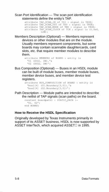
5-8 Data Formats
Scan Port Identification — The scan port identificationstatements define the entity’s TAP.attribute TAP_SCAN_IN of TDI : signal is TRUE;attribute TAP_SCAN_OUT of TDO : signal is TRUE; attribute TAP_SCAN_MODE of TMS : signal is TRUE; attribute TAP_SCAN_CLOCK of TCK : signal is (5.0e6, LOW);
Members Description (Optional) — Members representdevices or other modules that are on the module.Usually members represent components, but someboards may contain scannable daughtercards, cardslots, etc. that require member modules to describethem.attribute MEMBERS of BOARD : entity is“U1 (XYZ1, DW),”&“U2 (XYZ2, DW)”;
Bus Composition (Optional) — Buses in an HSDL modulecan be built of module buses, member module buses,member device buses, and member device testregisters.attribute BUS_COMPOSITION of BOARD : entity is“bus1[4] (U1.Boundary[3,0]),”&“bus2[4] (U2.Boundary[3,0])”;
Path Description — Module paths are intended to describethe netlist of TAP signals (scan paths) on the board.constant boardpath1 : STATIC_PATH :=“U1, U2”;
end BOARD;
How to Receive the HSDL Specification
Originally developed by Texas Instruments primarily insupport of its ASSET business, HSDL is now supported byASSET InterTech, which acquired ASSET in 1995.
5-9
Serial Vector Format (SVF)
Serial Vector Format, commonly referred to as SVF, wasjointly developed by Texas Instruments and Teradyne in1991. SVF is a standard ASCII format for expressing testpatterns that represent the stimulus, expected response, andmask data for IEEE Std 1149.1-based tests. The need forSVF arose from the desire to have vendor-independent IEEEStd 1149.1 test patterns that are transportable across a wideselection of simulation software and test equipment — fromdesign verification through field diagnostics.
Boundary-scan test execution is controlled by thesequencing of TAP signals on the pins of the devices. Eachdevice’s behavior is determined solely by the states of itsTAP pins. Boundary-scan tools must maintain knowledge ofthe sequences required to exert certain behaviors within adevice and where that device is located in the serial scanpath.
SVF controls the IEEE Std 1149.1 test bus using commandsthat transition the TAP from one steady state to another.Rather than describe the explicit state of the IEEE Std1149.1 bus on every TCK cycle, SVF describes it in terms oftransactions conducted between stable states. For instance,the process of scanning in an instruction is described merelyin terms of the data involved and the desired stable state toenter after the scan has been completed. The Capture,Update, Pause, etc. states are inferred rather than explicitlyrepresented. The data to be scanned in, expected data out,and compare mask are all grouped in an easilyunderstandable manner. A command is provided to supportdeterministic navigation of TAP states where required.
In addition to supporting higher level depictions of scanoperations, SVF also supports combined serial and paralleloperations. This allows SVF to accommodate ATEenvironments where some stimulus/response is handled viaparallel I/O, and serial signals are accessed via an IEEE Std1149.1-control environment.
SVF also supports the concept of scan offsets. Offsets allowa test to be applied to a component or cluster of logicembedded in the middle of a scan path. In Figure 5-1, adevice exists in multiple instances on a board. Seriallyapplied tests were generated by the designer that areavailable in SVF format. To reuse this test, it is necessary to
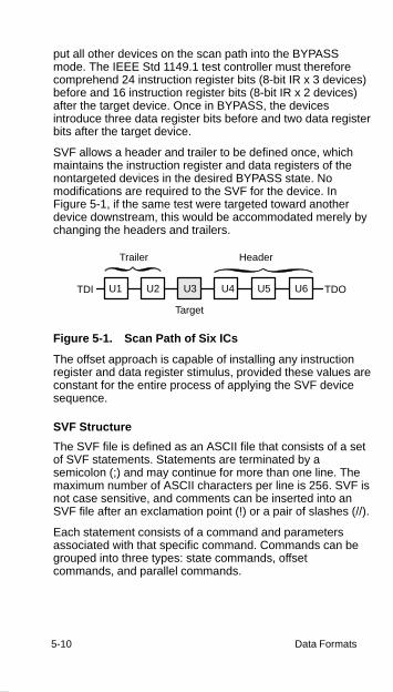
5-10 Data Formats
put all other devices on the scan path into the BYPASSmode. The IEEE Std 1149.1 test controller must thereforecomprehend 24 instruction register bits (8-bit IR x 3 devices)before and 16 instruction register bits (8-bit IR x 2 devices)after the target device. Once in BYPASS, the devicesintroduce three data register bits before and two data registerbits after the target device.
SVF allows a header and trailer to be defined once, whichmaintains the instruction register and data registers of thenontargeted devices in the desired BYPASS state. Nomodifications are required to the SVF for the device. InFigure 5-1, if the same test were targeted toward anotherdevice downstream, this would be accommodated merely bychanging the headers and trailers.
U1 U2 U3 U4 U5 U6TDI TDO
Trailer Header
Target
Figure 5-1. Scan Path of Six ICs
The offset approach is capable of installing any instructionregister and data register stimulus, provided these values areconstant for the entire process of applying the SVF devicesequence.
SVF Structure
The SVF file is defined as an ASCII file that consists of a setof SVF statements. Statements are terminated by asemicolon (;) and may continue for more than one line. Themaximum number of ASCII characters per line is 256. SVF isnot case sensitive, and comments can be inserted into anSVF file after an exclamation point (!) or a pair of slashes (//).
Each statement consists of a command and parametersassociated with that specific command. Commands can begrouped into three types: state commands, offsetcommands, and parallel commands.
5-11
State Commands
State commands are used to specify how the test sequenceswill traverse the IEEE Std 1149.1 TAP state machine. Thefollowing state commands are supported:
SDR Scan data registerSIR Scan instruction registerENDDR Define end state of DR scanENDIR Define end state of IR scanRUNTEST Enter Run-Test/Idle stateSTATE Go to specified stable stateTRST Drive the TRST line to the designated level
SDR performs an IEEE Std 1149.1 data register scan. SIRperforms an IEEE Std 1149.1 instruction register scan.ENDDR and ENDIR establish a default state for the busfollowing any data register scan or instruction register scan,respectively. RUNTEST goes to Run-Test/Idle state for aspecific number of TCKs. For each of the above commands,a default path through the state machine is used. Each ofthese commands also terminates in a stable, nonscannablestate.
STATE places the bus in a designated IEEE Std 1149.1stable state. TRST activates or deactivates the optionaltest-reset signal of the IEEE Std 1149.1 bus.
Offset Commands
Offset commands allow a series of SVF commands to betargeted toward a contiguous series of points in the scanpath. Examples would be a sequence for executing self-teston a device, or a cluster test where all devices involved inthe cluster test are grouped together. The following offsetcommands are supported:
HDR Header data for data bitsHIR Header data for instruction bitsTDR Trailer data for data bitsTIR Trailer data for instruction bits

5-12 Data Formats
HDR specifies a particular pattern of data bits to be paddedonto the front of every data scan. HIR specifies the same forthe front of every instruction register scan. TDR and TIRspecify data to be injected on the back of each scan. Thesepatterns need only be specified once and are included oneach scan unless changed by a subsequent HDR, HIR,TDR, or TIR command.
Parallel Commands
Parallel commands are used to map and apply the followingcommands:
PIO — Specifies a parallel test patternPIOMAP — Designates the mapping of bits in the PIOcommand to logical pin names
Parallel commands allow SVF to combine serial and parallelsequences. PIOMAP commands are used by parallel I/Ocontrollers to map data bits in the command into parallel I/Ochannels using the ASCII logical pin name as a reference.The PIO command specifies the execution of a parallelpattern application/sample. SVF does not specify any otherproperties of parallel I/O such as drive, levels, or skew.
Default State Transitions
SVF uses names for the TAP states that are similar to theIEEE Std 1149.1 TAP state names. Table 5-1 lists the SVFequivalent names for the TAP states.
5-13
Table 5-1. SVF TAP State Names
IEEE Std 1149.1 TAP State Name
SVF TAP State Name
Test-Logic-Reset RESET
Run-Test/Idle IDLE
Select-DR-Scan DRSELECT
Capture-DR DRCAPTURE
Shift-DR DRSHIFT
Pause-DR DRPAUSE
Exit1-DR DREXIT1
Exit2-DR DREXIT2
Update-DR DRUPDATE
Select-IR-Scan IRSELECT
Capture-IR IRCAPTURE
Shift-IR IRSHIFT
Pause-IR IRPAUSE
Exit1-IR IREXIT1
Exit2-IR IREXIT2
Update-IR IRUPDATE
5-14 Data Formats
Table 5-2 identifies sample default paths taken whentransitioning from one state to a specified new state. Forexample, if the current state is RESET and DRPAUSE isselected as the end state, the TAP moves from RESETthrough IDLE, DRSELECT, DRCAPTURE, DREXIT1 toDRPAUSE. One must only specify the current and end statesand not each intermediate step. See the TAP controller statediagram on page 3-5 of Chapter 3, Boundary-ScanArchitecture and IEEE Std 1149.1 to determine statetransition paths not shown in Table 5-2.
Table 5-2. Stable-State Path Examples
Current State End State State Path
RESET RESET RESET
RESET IDLE RESET
IDLE
RESET DRPAUSE RESET
IDLE
DRSELECT
DRCAPTURE
DREXIT1
DRPAUSE
RESET IRPAUSE RESET
IDLE
DRSELECT
IRSELECT
IRCAPTURE
IREXIT1
IRPAUSE
5-15
SVF Example
The following is an example SVF file:! Begin Test Program! Disable Test Reset line
TRST OFF;! Initialize UUT
STATE RESET;! End IR scans in DRPAUSE
ENDIR DRPAUSE;! End DR scans in DRPAUSE
ENDDR DRPAUSE;! 24 bit IR header
HIR 24 TDI (FFFFFF);! 3 bit DR header
HDR 3 TDI (7);! 16 bit IR trailer
TIR 16 TDI (FFFF);! 2 bit DR trailer
TDR 2 TDI (3);! 8 bit IR scan, load BIST opcode
SIR 8 TDI (41) TDO (81) MASK (FF);! 16 bit DR scan, load BIST seed
SDR 16 TDI (ABCD);! RUNBIST for 95 TCK Clocks
RUNTEST 95 TCK ENDSTATE IRPAUSE;! 16 bit DR scan, check BIST status
SDR 16 TDI (0000) TDO(1234) MASK(FFFF);! Enter Test-Logic-Reset
STATE RESET;! End Test Program
The test begins by deasserting TRST. The DRPAUSE stateis established as the default end state for instruction registerscans and data register scans. Twenty-four bits of headerand 16 bits of trailer data are specified for instruction registerscans. No status bits are checked. Three bits of header dataand two bits of trailer data are specified for data registerscans.
In the example above, a single device in the middle of thescan is targeted. Notice from the 24-bit IR header (3 x 8-bitIR) and the 3-bit DR header (3 x 1-bit DR) that the targeteddevice has three devices before it in the scan path. From the16-bit IR trailer (2 x 8-bit IR) and the 2-bit DR trailer (2 x 2-bitDR), the targeted device has two devices following it in thescan path. After the header and trailer offsets areestablished, all subsequent scans are the concatenation ofthe header, scan data, and trailer bits. The targeted devicesupports BIST, which is initialized by scanning hex 41 intothe instruction register, followed by hex ABCD into the
5-16 Data Formats
selected data register. The BIST in the targeted device isthen executed by entering the Run-Test/Idle state for95 clock cycles. Next, the BIST result is scanned out and thestatus bits compared against a deterministic value todetermine pass/fail.
How to Receive the SVF Specification
Orignally developed by Texas Instruments (with Teradyne)primarly in support of its ASSET business, SVF is nowsupported by ASSET InterTech, which acquired ASSETin 1995.
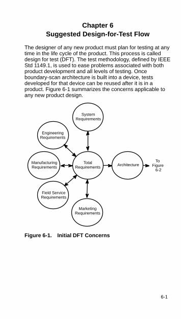
6-1
Chapter 6Suggested Design-for-Test Flow
The designer of any new product must plan for testing at anytime in the life cycle of the product. This process is calleddesign for test (DFT). The test methodology, defined by IEEEStd 1149.1, is used to ease problems associated with bothproduct development and all levels of testing. Onceboundary-scan architecture is built into a device, testsdeveloped for that device can be reused after it is in aproduct. Figure 6-1 summarizes the concerns applicable toany new product design.
ManufacturingRequirements
Field ServiceRequirements
MarketingRequirements
EngineeringRequirements
SystemRequirements
TotalRequirements Architecture
To Figure 6-2
Figure 6-1. Initial DFT Concerns
6-2 Suggested Design-for-Test Flow
Test RequirementsBefore implementing a boundary-scan test scheme, thedesigner must define test requirements for the followingphases of the product life cycle:
Design verification
Manufacturing test
Field test (also can be used for incoming inspection)
These studies must ensure that the necessary controls aredesigned into the hardware to support the followingrequirements:
During design verification, an engineer requirescontrollability of the circuitry, both internal to the IC and atboard and system levels. Design engineers needcontrollability and observability of every logic node in thesystem. If this proves to be unrealistic, reasonablecoverage is achievable with partial scan in aboundary-scan design.
Manufacturing test may include interconnect testing andfunctional logic validation.
Field or embedded testing typically may only include theability to report faults and to isolate a fault to afield-repairable unit (board or subsystem).
For both manufacturing test and field test, IEEE Std 1149.1logic and test vectors can be used to test clusters or blocksof logic.
Internal IC testing at the board or system level requires asubset of the complete IC logic-verification patterns tovalidate basic IC logic functions. Each level of hierarchicaltesting has a different set of fault characteristics. IEEE Std1149.1 logic can be used throughout the testing life cycle ofthe product.
6-3
Built-In Self-Test (BIST) MethodologyBIST usually consists of special circuitry built as part of anIC’s internal design. BIST tests typically perform thesefunctions:
Pseudorandom pattern generation (PRPG)
Parallel signature analysis (PSA)
Serial signature analysis (SSA)
State machine-based generation/comparison
IEEE Std 1149.1 commands can initiate BIST tests andreturn the test results.
Internal Scan Test MethodologyMany high-density microprocessors and ASICs now includeinternal IEEE Std 1149.1-compliant scan circuitry.High-pin-count and fine-pitch packages limit physical accessto package pins and devices with high gate count limitobservation of the internal logic states. Internal scan, eitherpartial or full, can do the following:
Provide access to internal registers
Partition the design
Reduce the design to combinatorial networks surroundedby scannable registers
Provide fast, efficient testing of internal logic
Internal scan also allows on-chip emulation control andcircuit observability within a device to provide designverification. The emulation capability also can aid in softwaredevelopment to control highly complex functions designedinto a device.
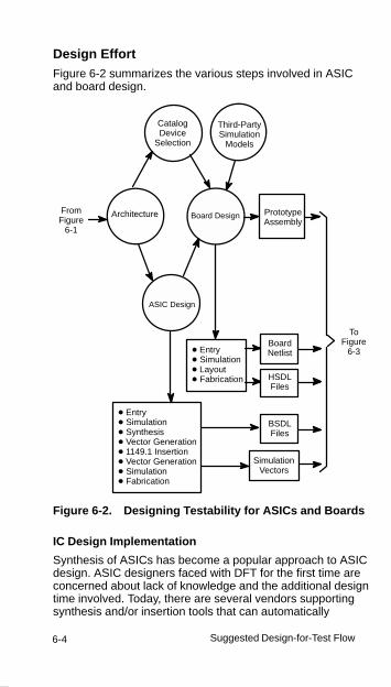
6-4 Suggested Design-for-Test Flow
Design EffortFigure 6-2 summarizes the various steps involved in ASICand board design.
Board Design
CatalogDevice
Selection
Architecture
Third-PartySimulation
Models
ASIC Design
� Entry� Simulation� Synthesis� Vector Generation� 1149.1 Insertion� Vector Generation� Simulation� Fabrication
� Entry� Simulation� Layout� Fabrication
BoardNetlist
HSDLFiles
SimulationVectors
BSDLFiles
FromFigure
6-1
ToFigure
6-3
PrototypeAssembly
Figure 6-2. Designing Testability for ASICs and Boards
IC Design Implementation
Synthesis of ASICs has become a popular approach to ASICdesign. ASIC designers faced with DFT for the first time areconcerned about lack of knowledge and the additional designtime involved. Today, there are several vendors supportingsynthesis and/or insertion tools that can automatically
6-5
generate the following elements of an IEEE Std 1149.1architecture:
Test access port (TAP) controller
Instruction register
Instruction decode logic
Bypass register
Boundary-scan register
Such tools also can automatically generate test vectors forIEEE Std 1149.1-compliant designs. This means that adesigner can quickly and correctly implement basic IEEE Std1149.1 test circuitry in an ASIC.
If synthesis is not available, most ASIC vendors offer alibrary of macros that the designer can use to implementIEEE Std 1149.1 into their designs. Using vendor macrosrequires considerably more effort and knowledge toimplement IEEE Std 1149.1 into an ASIC, compared to usingsynthesis. However, in the absence of synthesis orboundary-scan insertion tools, using vendor macros issignificantly easier than implementing boundary-scanarchitecture using a library that has no such macros. TexasInstruments offers a family of IEEE Std 1149.1-compliantASIC macros for gate array and standard cell designs.
The ASIC designer is required to provide a Boundary-ScanDescription Language (BSDL) file that describes the finishedASIC. This information becomes the basis for tools thatautomatically create board interconnect test vectors. Thesevectors can be used by the board designer for debug andvalidation and by manufacturing test departments for qualityassurance.
Several DFT tool vendors plan to implement automatic BSDLcreation that is available once the ASIC design has beencompleted. The creation of a BSDL file by the ASIC designeris straightforward if the design tool used does notautomatically create it.

6-6 Suggested Design-for-Test Flow
IC Simulation
During IC simulation, the designer can use IEEE Std 1149.1logic to simplify the simulation patterns required to validatethe design. First, patterns must be developed to verify thatthe IEEE Std 1149.1 interface is operating properly. SimpleIR and DR scan patterns can be developed to perform thischeck. If internal scan is implemented, then simulationpattern sets can be written to test internal logic clusters usingthe internal scan registers. This partitioned approachsimplifies design validation.
Using SVF for IC Design Validation
Many IEEE Std 1149.1-compliant tools use Serial VectorFormat (SVF) as the primary test pattern data format andinterfaces between simulators and ATE testers also supportSVF.
A collection of manually-generated SVF patterns, simulationpatterns translated into SVF and ATPG-generated SVFpatterns can be used to validate the IEEE Std 1149.1 logic.Initial tests must first verify that serial data can be scannedinto and out of the IC. Proper use of internal scan registers topartition the internal functional logic can simplify faultdetection and isolation.
IC testing usually is broken into three parts; static functionaltests at 1 MHz, at-speed functional tests, and parametrictests. Because IEEE Std 1149.1 architecture relies onserially scanning control and test data, only static functionaltesting and DC parametric testing can be performed via theIEEE Std 1149.1 architecture. However, the IEEE Std 1149.1TAP can be used to access user-defined test instructions(such as RUNBIST), which can be operated at speed.
INTEST patterns generated by a simulator can be used tovalidate the internal logic of the IC. By comparing thesepatterns with simulation results and by observing internalscan register contents, the designer can isolate faultyinternal logic. Figure 6-3 summarizes the design validationflow for all products, from IC through system-level products.
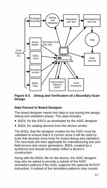
6-7
BoardNetlist
HSDLFiles
SimulationVectors
BSDLFiles
Debugand
Validation
FieldService
Manufacturingand Test
Integrationand Test
Ship
InterconnectPatterns
(SVF)
Fault Dictionary
Boundary-ScanTest Tool
FromFigure
6-2
PrototypeAssembly
Figure 6-3. Debug and Verification of a Boundary-ScanDesign
Data Passed to Board Designer
The board designer needs test data to use during the designdebug and validation phase. This data includes:
BSDL for the ASICs as developed by the ASIC designer
BSDL for catalog devices from the device vendor
The BSDL that the designer creates for the ASIC must bevalidated to ensure that it is correct since it will be used bytools that develop more tests for board debug and validation.The new tests are then applicable for manufacturing test andfield service test vector generation. BSDL created by asynthesis tool should accurately reflect a device’sconstruction.
Along with the BSDL file for the device, the ASIC designermay also be asked to provide a subset of the ASICsimulation patterns if the ASIC supports the optional INTESTinstruction. A subset of the simulation patterns may consist

6-8 Suggested Design-for-Test Flow
of the static (1-MHz) functional patterns. Only a subset ofpatterns may be needed because it may be impractical toreapply the entire static functional test pattern set at theboard level. Many companies have found that they canachieve an acceptable level of confidence that the ASIC isfunctioning correctly using only a portion of the entire staticfunctional pattern set.
Board DesignMost of the concepts described for IC design also apply toboard and system integration. BSDL is used to describe theIEEE Std 1149.1 scan architecture of an IC, and HierarchicalSystem Description Language (HSDL) is used to describesubsystems and systems. HSDL is used to describe thescan architecture, group discrete signals into logical groups(e.g., ADDR0–15, DATA0–7) and to define constraints.
ConstraintsA constraint defines a logic condition that can applypotentially harmful signals to a circuit. IEEE Std 1149.1 givesdirect control of all scannable signals, so it is possible tocreate logic states that functionally would not be entered. Forexample, bus-arbitration logic can be overridden anddangerous hardware conditions or conflict can occur. Anexample of a constraint is to inhibit any test pattern thatwould cause two scannable output nodes to drive a commonbus net at the same time.
Partitioned Scan PathAt the board level, the designer must consider how topartition the IEEE Std 1149.1 scan path. Commercial devicesare available (such as TI’s SN74ACT8997† SPL) to switch asingle primary scan path to one or more multiple secondaryscan paths. The designer should consider the benefits andpenalties associated with partitioned scan paths.
† SN54ACT8997, SN74ACT8997 Scan Path Linkers With 4-Bit IdentificationBuses, Literature Number SCAS157C, Texas Instruments 1996.
6-9
Penalties associated with partitioned scan paths include:
Scan overhead required to switch from one partition toanother
Timing delays in routing TMS (affecting scan frequency)
Added complexity of the IEEE Std 1149.1 test program
Benefits associated with partitioned scan paths include:
Shorter scan paths
Additional fault tolerance
Somewhat simplified test software
Board Validation/Manufacturing TestThe IEEE Std 1149.1 architecture has the ability to detect,and in many cases, isolate a scan path fault. The instructionregister definition requires that the two (2) least-significantbits (those closest to TDO) of a device be, respectively, alogic 1, followed by a logic 0 during an IR scan. This ruleallows the IEEE Std 1149.1-compliant bus controller toperform a simple IR scan to prove all devices on the bus candrive a logic 1 and logic 0 on the TDI–TDO path. There areATPG tools available that automatically generate SVF busvalidation patterns that can be applied by the bus controller.
The primary objective of IEEE Std 1149.1 is to allow controland observation of device input and output pins for thepurpose of interconnect testing. The reduced size of ICpackages has made interconnect testing of PWBs difficultand expensive when using conventional interconnect testing.Commercial tools are available that automatically generateSVF patterns for interconnect testing. Such tools input aboard netlist and the BSDL of the scannable componentsand output an SVF pattern set. This pattern set, along with afault dictionary lookup table, allows an IEEE Std 1149.1 buscontroller to apply the interconnect patterns to the board anddetect/isolate faulty interconnections.
6-10 Suggested Design-for-Test Flow
After proving correct operation of the IEEE Std 1149.1 busand board interconnect, the designer can control andobserve all boundary-scan nodes. Commercially availableboundary-scan test tools allow interactive, macro, orhigh-level-language programming control for the designer.The board designer also can import and reapply the SVFpatterns developed by the IC designer. This reuse of patternsets provides these benefits:
Knowledge is passed from one designer to another.
Overall product development cycle is reduced.
Using common SVF patterns reduces ambiguity betweenhierarchical test levels.
The SVF pattern set developed by the IC designer tests anindividual IC. The board designer has to be able to relocatethe relative scan position of the IC SVF test to match its scanposition on the board dynamically. SVF headers and trailerscan be manipulated by the boundary-scan test tool to allowsuch dynamic test relocation.
SummaryAs designers become better acquainted with IEEE Std1149.1, they will no doubt find benefits well beyond thosediscussed in this chapter. The standard became availablejust in time to offer solutions and benefits to customersexperiencing complex problems introduced by newtechnology.
The benefits that customers can realize from IEEE Std1149.1 architecture include:
Reuse test data throughout the product life cycle
Apply off-the-shelf components, tools, and ATE solutionsfrom multiple vendors
Maintain common data base formats for these benefits:Shared common databases between IC, board, andsystem designers (BSDL, HSDL)Reusable pattern sets (SVF)Reusable test pattern set (TPS) code
7-1
Chapter 7Applications
This chapter presents a number of testing problems andshows how boundary-scan testing and TI products can beused to solve them.
Board-Etch and Solder-Joint TestingThe current approach to detecting board-etch andsolder-joint faults in today’s electronics industry uses twoforms of automatic test equipment (ATE): bare-board testersand digital in-circuit testers. Bare-board test is done afterboard fabrication. Tests for open-etch circuits between nodesforce a voltage onto one circuit node and sense the voltageat another circuit node. This technique is used only on a raw,unassembled board.
An in-circuit test is done after board assembly and checksfor:
Correct orientation of parts
Correct value and type of parts
Correct solder joints between all parts and the board
Software models of each part on a board are used togenerate the test patterns used by the in-circuit tester. Themain assumption is that both board and in-circuit testersrequire physical access to nodes or points on the board toperform the necessary testing. Both testers require the abilityto inject a voltage or current onto a nodal network and sensethe voltage or current at another point on the network.
Higher-density packaging technologies, finer-pitch boardetch, and more complex digital integrated circuits have madebare-board and in-circuit testing much more expensive.
Solution
Several testability products from Texas Instruments lendthemselves to support IC-to-IC continuity testing. Thetechniques outlined allow detection and, in most cases,isolation of board-etch and solder-joint faults, without forcingany additional requirements on the electrical designengineer. ASIC devices and bus-interface components with
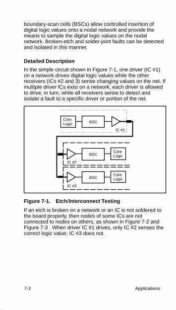
7-2 Applications
boundary-scan cells (BSCs) allow controlled insertion ofdigital logic values onto a nodal network and provide themeans to sample the digital logic values on the nodalnetwork. Broken-etch and solder-joint faults can be detectedand isolated in this manner.
Detailed Description
In the simple circuit shown in Figure 7-1, one driver (IC #1)on a network drives digital logic values while the otherreceivers (ICs #2 and 3) sense changing values on the net. Ifmultiple driver lCs exist on a network, each driver is allowedto drive, in turn, while all receivers sense to detect andisolate a fault to a specific driver or portion of the net.
CoreLogic BSC
CoreLogic
CoreLogic
IC #1
IC #2
IC #3
BSC
BSC
Figure 7-1. Etch/Interconnect Testing
If an etch is broken on a network or an IC is not soldered tothe board properly, then nodes of some ICs are notconnected to nodes on others, as shown in Figure 7-2 andFigure 7-3 . When driver IC #1 drives, only IC #2 senses thecorrect logic value; IC #3 does not.
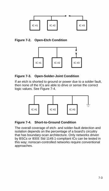
7-3
IC #1 IC #2 IC #3
Figure 7-2. Open-Etch Condition
IC #1 IC #2 IC #3
Figure 7-3. Open-Solder-Joint Condition
If an etch is shorted to ground or power due to a solder fault,then none of the ICs are able to drive or sense the correctlogic values. See Figure 7-4.
IC #1 IC #2 IC #3
Figure 7-4. Short-to-Ground Condition
The overall coverage of etch- and solder-fault detection andisolation depends on the percentage of a board’s circuitrythat has boundary-scan architecture. Only networks drivenby BSCs or IEEE Std 1149.1-compliant ICs can be tested inthis way; nonscan-controlled networks require conventionalapproaches.
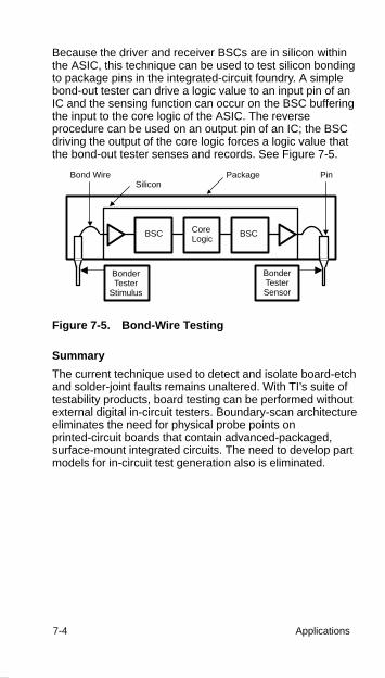
7-4 Applications
Because the driver and receiver BSCs are in silicon withinthe ASIC, this technique can be used to test silicon bondingto package pins in the integrated-circuit foundry. A simplebond-out tester can drive a logic value to an input pin of anIC and the sensing function can occur on the BSC bufferingthe input to the core logic of the ASIC. The reverseprocedure can be used on an output pin of an IC; the BSCdriving the output of the core logic forces a logic value thatthe bond-out tester senses and records. See Figure 7-5.
BSC
Bond WireSilicon
Package Pin
CoreLogic
BSC
BonderTester
Stimulus
BonderTesterSensor
Figure 7-5. Bond-Wire Testing
Summary
The current technique used to detect and isolate board-etchand solder-joint faults remains unaltered. With TI’s suite oftestability products, board testing can be performed withoutexternal digital in-circuit testers. Boundary-scan architectureeliminates the need for physical probe points onprinted-circuit boards that contain advanced-packaged,surface-mount integrated circuits. The need to develop partmodels for in-circuit test generation also is eliminated.
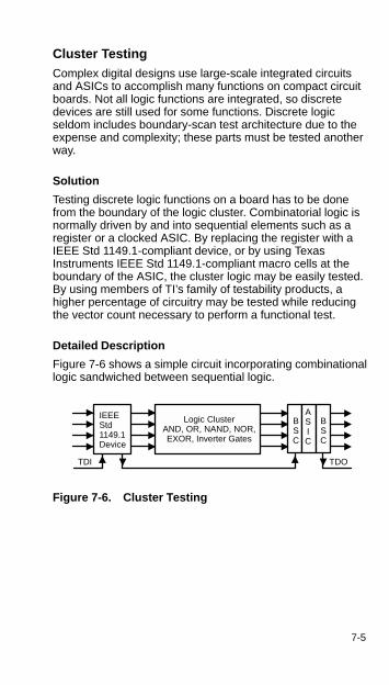
7-5
Cluster TestingComplex digital designs use large-scale integrated circuitsand ASICs to accomplish many functions on compact circuitboards. Not all logic functions are integrated, so discretedevices are still used for some functions. Discrete logicseldom includes boundary-scan test architecture due to theexpense and complexity; these parts must be tested anotherway.
Solution
Testing discrete logic functions on a board has to be donefrom the boundary of the logic cluster. Combinatorial logic isnormally driven by and into sequential elements such as aregister or a clocked ASIC. By replacing the register with aIEEE Std 1149.1-compliant device, or by using TexasInstruments IEEE Std 1149.1-compliant macro cells at theboundary of the ASIC, the cluster logic may be easily tested.By using members of TI’s family of testability products, ahigher percentage of circuitry may be tested while reducingthe vector count necessary to perform a functional test.
Detailed Description
Figure 7-6 shows a simple circuit incorporating combinationallogic sandwiched between sequential logic.
IEEEStd1149.1Device
Logic ClusterAND, OR, NAND, NOR,EXOR, Inverter Gates
BSC
ASIC
TDI TDO
BSC
Figure 7-6. Cluster Testing
7-6 Applications
During normal circuit operation, the IEEE Std1149.1-compliant device drives the glue logic through to theBSCs in the ASIC. Two methods may be used to perform atest of the logic cluster using the TI family of testabilityproducts. There are benefits and drawbacks to bothmethods.
1. Method one is to scan a fixed-order set of test patternscalled deterministic test vectors into the IEEE Std1149.1-compliant device and sample the resultant data atthe ASIC boundary.
2. Method two is to command the IEEE Std 1149.1-compliantdevice to output a pseudorandom pattern of data while theASIC performs a parallel signature analysis of its inputs.
Deterministic Test Vectors
Deterministic test vectors scanned into the UUT can pinpointa problem more easily than signature analysis. Since theexact input stimulus is known, the failing response can bedetected. Deterministic test vectors perform a complete andmeaningful test, but consume a lot of time and enoughmemory to store all vector data for both stimulus andresponse.
Signature Analysis
Signature analysis can be performed quickly and virtuallyautomatically. After valid pattern generation and signatureanalysis seed values are obtained, the resultant signaturecan be checked against the correct value. This test can beperformed at the scan clock speed and requires very littlememory for data storage. However, the fault cannot belocated without using an extensive fault dictionary.
Signature analysis requires that the IEEE Std1149.1-compliant device be able to generate stimuluspatterns and the ASIC be able to capture a signature of itsinputs. This means that appropriate macro cells must beused as outputs of the driving device and as inputs to theboundary of the ASIC. These cells require additional spaceand additional circuitry to be incorporated into each BSC.
Summary
Using the IEEE Std 1149.1-compliant family of testabilityproducts from Texas Instruments enables designers to add
7-7
features previously unachievable in their designs. It isbeneficial to test glue-logic clusters using existingboundary-scan components that surround the logic cluster.This provides added value to the boundary-scan overheadbuilt into a design’s larger devices.
Board-Edge Connector TestingBoard-to-board fault detection and isolation within a digitalsystem have historically depended primarily on built-in test(BIT) software. This approach is adequate for detectingfunctional faults on boards, assuming that the processorexecuting BIT software can access the boards installed inthe system. Backplane faults typically manifest themselves inthese ways:
Broken or bent pins on connectors
Broken etch on a backplane motherboard
Termination-network fault
Bus contention on a bused network
Many bus faults in today’s digital processor environments areso catastrophic in nature that the processor executing BITcannot access the boards installed within the system toisolate the fault.
Solution
In much the same way that boundary scan allows detectionand isolation of etch and solder-joint faults on a PWB,surrounding the bus interface of a board with IEEE Std1149.1-compliant devices allows detection and isolation ofbus and connector faults. By placing IEEE Std1149.1-compliant devices in a controlled test mode, eachboard, in turn, can drive the backplane bus while the otherboards receive the driven logic values.
Detailed Description
Broken etch on a motherboard backplane presents problemssimilar to that of broken etch on a PWB connectingintegrated circuits; some boards cannot communicate toothers past the etch break (see Figure 7-7). By placing thetestability devices on each board into a controlled test mode,
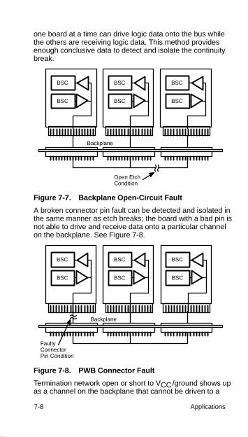
7-8 Applications
one board at a time can drive logic data onto the bus whilethe others are receiving logic data. This method providesenough conclusive data to detect and isolate the continuitybreak.
BSC
BSC
BSC
BSC
BSC
BSC
Backplane
Open EtchCondition
Figure 7-7. Backplane Open-Circuit Fault
A broken connector pin fault can be detected and isolated inthe same manner as etch breaks; the board with a bad pin isnot able to drive and receive data onto a particular channelon the backplane. See Figure 7-8.
Backplane
BSC
BSC
BSC
BSC
BSC
BSC
Faulty Connector Pin Condition
Figure 7-8. PWB Connector Fault
Termination network open or short to VCC/ground shows upas a channel on the backplane that cannot be driven to a

7-9
certain logic state. The characteristic of this fault could beconfused with a bus contention fault. See Figure 7-9.
Backplane
BSC
BSC
BSC
BSC
BSC
BSC
Short-to-GroundCondition
Figure 7-9. Backplane Short-to-Ground Fault
Bus contention faults occur when a three-state bus driver isstuck in a functional-enable mode. The BSCs in a controlledmode can be disabled by the test circuitry, thus bypassingthe functional-enable control. All of the tests described canbe executed offline in a test mode or by built-in test (BIT)software interfacing to an IEEE Std 1149.1-compliant serialscan controller in the system.
Summary
Board-to-board fault detection and isolation in a controlledoffline test mode and concurrent background BIT executioncan be dramatically improved by using boundary-scantestability devices within the bus interface circuitry of eachboard installed in a system. Boundary-scan architecture atthe backplane-interface can increase fault isolation bymasking some interface logic from the circuitry under test.
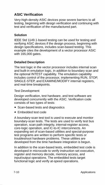
7-10 Applications
ASIC VerificationVery-high-density ASIC devices pose severe barriers to alltesting, beginning with design verification and continuing withtest and verification of the manufactured part.
Solution
IEEE Std 1149.1-based testing can be used for testing andverifying ASIC devices if the design process, beginning withdesign specifications, includes scan-based testing. Thisexample cites the development of a vector processor ASICwith 165,000 gates.
Detailed Description
The test logic in the vector processor includes internal scanand built-in emulation logic, in addition to boundary scan andthe optional INTEST capability. The emulation capabilityincludes control of the processor, implementing RUN, STOP,SINGLE-STEP, and EXAMINE/MODIFY internal registers,and real-time breakpoints.
Test Development
Design verification, test hardware, and test software aredeveloped concurrently with the ASIC. Verification codeconsists of two types of tests:
Scan-based tests and diagnostics
Embedded test code
A boundary-scan test tool is used to execute and monitorboundary-scan tests. The tests are used to verify test busoperation, scan path integrity, internal-register access,core-logic operation, and IC-to-IC interconnects. Anexpanding set of scan-based utilities and special-purposetest programs are written to perform specific tests ortroubleshoot hardware problems. These utilities aredeveloped from the time hardware integration is begun.
In addition to the scan-based tests, embedded test code isdeveloped in microcode to verify instruction set execution,register and memory decode, memory access, andinput/output operations. The embedded tests targetfunctional logic and verify at-speed operations.
7-11
Design Verification
The vector processor ASIC in the design incorporatesextensive internal scan paths and breakpoint logic controlledvia the IEEE Std 1149.1 test bus. Key registers that areaccessible via scan include the address and data registerfiles, ALU and multiplier pipeline registers, and the programinstruction register.
Initial checkout of the vector processor includes scan pathintegrity and internal register access using internal scan andboundary scan. The first devices contain nonfunctionalmicrocode RAM, therefore an alternate plan is devised touse IEEE Std 1149.1 to validate all other circuitry.
The vector processor checkout uses the boundary-scanarchitecture to perform register reads and writes and simpleoperations to verify microcode execution. Simple microcodeoperations are tested by scanning an opcode into theinstruction register and clocking the processor usingboundary scan.
A test routine is developed in C++ that automates themicrocode execution steps. The program readsmicrocode-object files, scans the instruction into theinstruction register, clocks the processor, and reads theprogram counter to locate the next instruction. As eachinstruction is executed, the program dumps the accumulatorand status registers to allow monitoring of each instruction.This process is repeated for each microcode routine until allmicrocode is executed and nearly all processor functions areverified using the “bad” vector processors. Many weeks aresaved while waiting for new vector processors.
Summary
Design verification, hardware test, and software integrationrepresent significant challenges. Anticipating this, manydesign-for-test and integration capabilities need to beincorporated into the device to ensure controllability andobservability of embedded functions. IEEE Std 1149.1provides the primary method for design verification,hardware/software integration, and hardware test.
Test and interaction issues in this case were aggravated bythe lack of physical access caused by the small geometry ofthe module. Boundary-scan testing saved a significant
7-12 Applications
portion of the design verification effort that would have beenrequired for the less-effective conventional physical accessmethods.
Memory-Testing TechniquesThe steady increase in memory density has led to theincreased use of high-capacity memory boards in today’selectronic systems. It has also encouraged the use ofembedded memory within microprocessors, digital signalprocessors (DSP), and ASICs. As a result, testing of theseboards and devices has become more complex.Large-capacity memory boards require very long testexecution times for adequate fault detection. Large bus sizes(32 bits) and high bus fanout further complicate the problemof isolating component faults. Embedded memories, whichoften make up a significant portion of the device area, createadditional difficulties due to a lack of test access.
Solution
The use of scan-path technologies can simplify the problemof testing large memory arrays within a system or embeddedmemories within a device. Scan-path devices such as TI’sbus-interface components can be used to partition largememory device arrays into smaller, more easily testablearrays to increase component fault isolation. In addition, theuse of TI’s IEEE Std 1149.1-compliant macro cells withinASIC devices provides controllability and observability ofembedded memory that is normally inaccessible. Memorytest times can be reduced through the efficient partitioningand testing of several memory arrays (on a board or within adevice) in parallel.
Detailed Description
Figure 7-10 shows a 256 × 8 memory array, associated businterface, and control logic configured to test variousmemory-pattern-generation techniques. This configurationallows for explicit read/write operations using IEEE Std1149.1 EXTEST and SAMPLE instructions. In addition, thecomponents have a BIST capability (controlled by IEEE Std1149.1 instructions) used to perform memory read/writeoperations. The test results shown in Table 7-1 compareexplicit scanning in the RAM array address, data, and strobe
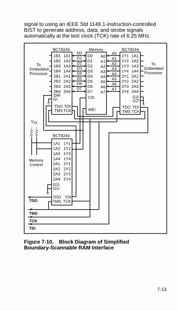
7-13
signal to using an IEEE Std 1149.1-instruction-controlledBIST to generate address, data, and strobe signalsautomatically at the test clock (TCK) rate of 6.25 MHz.
To EmbeddedProcessor
1A11A21A31A42A12A22A32A4
1Y11Y21Y31Y42Y12Y22Y32Y4
1B11B21B31B42B12B22B32B4
A0A1A2A3A4A5A6A7
D0D1D2D3D4D5D6D7
1A11A21A31A42A12A22A32A4
1A11A21A31A42A12A22A32A4
1Y11Y21Y31Y42Y12Y22Y32Y4
G2\G\
G2\G1\
DIR G1\
WE\TDOTMS
TDITCK
TDOTMS
TDITCK
TDOTMS
TDITCK
CS\
TDO
TMS
TDI
TCK
Vcc
MemoryControl
Memory’BCT8245 ’BCT8244D0D1D2D3D4D5D6D7
A0A1A2A3A4A5A6A7
’BCT8244
To EmbeddedProcessor
Figure 7-10. Block Diagram of SimplifiedBoundary-Scannable RAM Interface
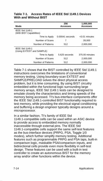
7-14 Applications
Table 7-1. Access Rates of IEEE Std 1149.1 DevicesWith and Without BIST
Mode256
Accesses1,000,000Accesses
IEEE Std 1149.1 (With BIST Capabilities)
Time to Apply 0.00041 seconds <0.01 minutes
Number of Scans 7 28,000
Number of Patterns 512 2,000,000
IEEE Std 1149.1 (Using EXTEST and SAMPLE)
Time to Apply 5.625 seconds 375.00 minutes
Number of Scans 512 2,000,000
Number of Patterns 512 2,000,000
Table 7-1 shows that the BIST controlled by IEEE Std 1149.1instructions overcomes the limitations of conventionalmemory testing. Using boundary-scan EXTEST andSAMPLE/PRELOAD solves the direct physical accessproblem, but it is time consuming. By using BIST circuitryembedded within the functional logic surrounding largememory arrays, IEEE Std 1149.1 tests can be designed toemulate closely the characteristics and timing speeds of thememory being accessed. TI’s bus-interface components offerthe IEEE Std 1149.1-controlled BIST functionality required totest memory, while providing the electrical signal conditioningand buffering a design engineer typically designs around amicroprocessor.
In a similar fashion, TI’s family of IEEE Std1149.1-compatible cells can be used within an ASIC deviceto provide access to embedded memory normallyinaccessible through external pins. The IEEE Std1149.1-compatible cells support the same self-test featuresas the bus-interface devices (PRPG, PSA, Toggle 1/0modes), which further simplify memory testing. Additionalfeatures such as programmable PRPG and PSA taps, built-incomparison logic, maskable PSA/comparison inputs, andbidirectional cells provide even more flexibility in self-testdesign. These features can be used with a built-in testcontroller to create an autonomous BIST for the memoryarray and/or other functions within the device.
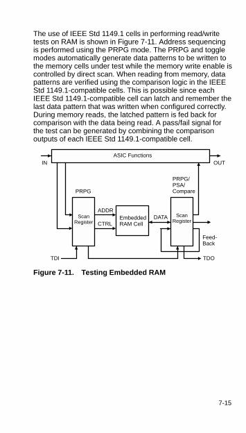
7-15
The use of IEEE Std 1149.1 cells in performing read/writetests on RAM is shown in Figure 7-11. Address sequencingis performed using the PRPG mode. The PRPG and togglemodes automatically generate data patterns to be written tothe memory cells under test while the memory write enable iscontrolled by direct scan. When reading from memory, datapatterns are verified using the comparison logic in the IEEEStd 1149.1-compatible cells. This is possible since eachIEEE Std 1149.1-compatible cell can latch and remember thelast data pattern that was written when configured correctly.During memory reads, the latched pattern is fed back forcomparison with the data being read. A pass/fail signal forthe test can be generated by combining the comparisonoutputs of each IEEE Std 1149.1-compatible cell.
EmbeddedRAM Cell
ADDR
CTRLDATA
ASIC Functions
PRPG
PRPG/PSA/Compare
Feed-Back
IN
TDI TDO
OUT
ScanRegister
ScanRegister
Figure 7-11. Testing Embedded RAM
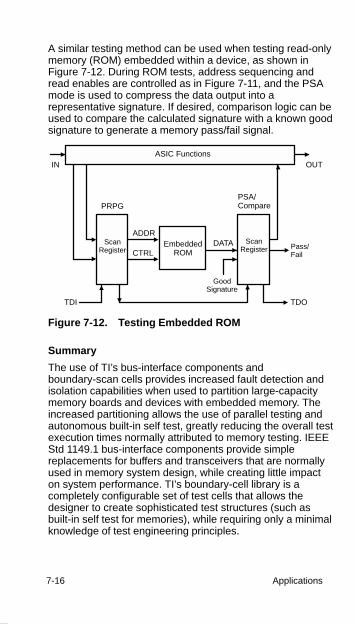
7-16 Applications
A similar testing method can be used when testing read-onlymemory (ROM) embedded within a device, as shown inFigure 7-12. During ROM tests, address sequencing andread enables are controlled as in Figure 7-11, and the PSAmode is used to compress the data output into arepresentative signature. If desired, comparison logic can beused to compare the calculated signature with a known goodsignature to generate a memory pass/fail signal.
EmbeddedROM
ADDR
CTRLDATA
ASIC Functions
PRPG
IN
TDI TDO
OUT
ScanRegister Pass/
Fail
GoodSignature
PSA/Compare
ScanRegister
Figure 7-12. Testing Embedded ROM
Summary
The use of TI’s bus-interface components andboundary-scan cells provides increased fault detection andisolation capabilities when used to partition large-capacitymemory boards and devices with embedded memory. Theincreased partitioning allows the use of parallel testing andautonomous built-in self test, greatly reducing the overall testexecution times normally attributed to memory testing. IEEEStd 1149.1 bus-interface components provide simplereplacements for buffers and transceivers that are normallyused in memory system design, while creating little impacton system performance. TI’s boundary-cell library is acompletely configurable set of test cells that allows thedesigner to create sophisticated test structures (such asbuilt-in self test for memories), while requiring only a minimalknowledge of test engineering principles.
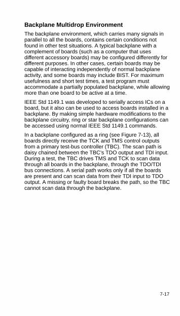
7-17
Backplane Multidrop EnvironmentThe backplane environment, which carries many signals inparallel to all the boards, contains certain conditions notfound in other test situations. A typical backplane with acomplement of boards (such as a computer that usesdifferent accessory boards) may be configured differently fordifferent purposes. In other cases, certain boards may becapable of interacting independently of normal backplaneactivity, and some boards may include BIST. For maximumusefulness and short test times, a test program mustaccommodate a partially populated backplane, while allowingmore than one board to be active at a time.
IEEE Std 1149.1 was developed to serially access ICs on aboard, but it also can be used to access boards installed in abackplane. By making simple hardware modifications to thebackplane circuitry, ring or star backplane configurations canbe accessed using normal IEEE Std 1149.1 commands.
In a backplane configured as a ring (see Figure 7-13), allboards directly receive the TCK and TMS control outputsfrom a primary test-bus controller (TBC). The scan path isdaisy chained between the TBC’s TDO output and TDI input.During a test, the TBC drives TMS and TCK to scan datathrough all boards in the backplane, through the TDO/TDIbus connections. A serial path works only if all the boardsare present and can scan data from their TDI input to TDOoutput. A missing or faulty board breaks the path, so the TBCcannot scan data through the backplane.
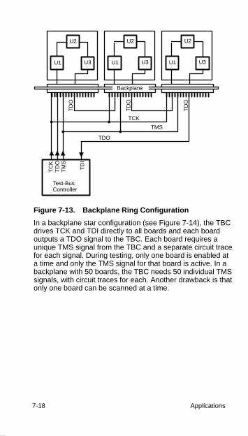
7-18 Applications
U1
U2
U3 U1
U2
U3 U1
U2
U3
TDO
Test-BusController
TMS
TC
KT
DO
TM
S
TD
I
TCK
Backplane
TD
O
TD
O
TD
O
Figure 7-13. Backplane Ring Configuration
In a backplane star configuration (see Figure 7-14), the TBCdrives TCK and TDI directly to all boards and each boardoutputs a TDO signal to the TBC. Each board requires aunique TMS signal from the TBC and a separate circuit tracefor each signal. During testing, only one board is enabled ata time and only the TMS signal for that board is active. In abackplane with 50 boards, the TBC needs 50 individual TMSsignals, with circuit traces for each. Another drawback is thatonly one board can be scanned at a time.
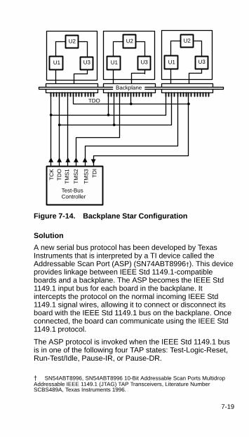
7-19
TDO
U1
U2
U3 U1
U2
U3
Test-BusController
TC
KT
DO
TM
S1
TD
I
TM
S2
TM
S3
U2
U3U1
Backplane
Figure 7-14. Backplane Star Configuration
Solution
A new serial bus protocol has been developed by TexasInstruments that is interpreted by a TI device called theAddressable Scan Port (ASP) (SN74ABT8996�). This deviceprovides linkage between IEEE Std 1149.1-compatibleboards and a backplane. The ASP becomes the IEEE Std1149.1 input bus for each board in the backplane. Itintercepts the protocol on the normal incoming IEEE Std1149.1 signal wires, allowing it to connect or disconnect itsboard with the IEEE Std 1149.1 bus on the backplane. Onceconnected, the board can communicate using the IEEE Std1149.1 protocol.
The ASP protocol is invoked when the IEEE Std 1149.1 busis in one of the following four TAP states: Test-Logic-Reset,Run-Test/Idle, Pause-IR, or Pause-DR.
� SN54ABT8996, SN54ABT8996 10-Bit Addressable Scan Ports MultidropAddressable IEEE 1149.1 (JTAG) TAP Transceivers, Literature NumberSCBS489A, Texas Instruments 1996.
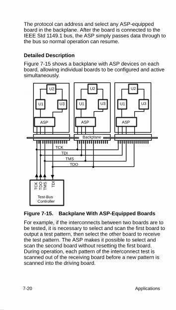
7-20 Applications
The protocol can address and select any ASP-equippedboard in the backplane. After the board is connected to theIEEE Std 1149.1 bus, the ASP simply passes data through tothe bus so normal operation can resume.
Detailed Description
Figure 7-15 shows a backplane with ASP devices on eachboard, allowing individual boards to be configured and activesimultaneously.
ASP
TDITMS
TDO
TCK
U1
U2
U3
ASP
U1
U2
U3
ASP
U1
U2
U3
Test-BusController
TC
KT
DO
TM
S
TD
I
Backplane
Figure 7-15. Backplane With ASP-Equipped Boards
For example, if the interconnects between two boards are tobe tested, it is necessary to select and scan the first board tooutput a test pattern, then select the other board to receivethe test pattern. The ASP makes it possible to select andscan the second board without resetting the first board.During operation, each pattern of the interconnect test isscanned out of the receiving board before a new pattern isscanned into the driving board.
7-21
Another test may be to select and initiate self-tests in aselected group of backplane boards. The ASP allows BIST tostart on each board and run while other board tests areinitialized. Each board is then polled to read the test results,one board at a time.
Summary
The special problems associated with backplane testing canbe accommodated when the SN74ABT8996 AddressableScan Port is added to individual boards.
Embedded ApplicationsField testing can be simplified if equipment is configured totake advantage of embedded IEEE Std 1149.1 functions.
Solution
TI’s SN74ACT8990† Test-Bus Controller (TBC) andSN74LVT8980‡ Embedded Test-Bus Controller (eTBC)devices can be embedded in system circuitry to provideautonomous IEEE Std 1149.1-based testing. A licensable,embeddable “C” source code product called Scan Engine,which includes test vector translators, is available to simplifyembedded boundary-scan test applications.
Detailed Description
TI’s test-bus controller devices operate under the control of ahost processor to master one or more IEEE Std 1149.1 scanpaths. Appearing to the host as memory- or I/O-mappedperipherals, they accept parallel command and test data andconvert it to appropriate IEEE Std 1149.1 protocols, asrequired. Thus, they allow the host software to operate at ahigh-level (essentially, at the level of SVF) rather thanrequiring that it encode knowledge of TMS state,sequencing, etc.
† SN54ACT8990, SN74ACT8990 Test-Bus Controllers, Literature NumberSCAS190C, Texas Instruments 1996.‡ SN54LVT8980, SN74LVT8980 Embedded Test-Bus Controllers, LiteratureNumber SCBS676, Texas Instruments 1996.
7-22 Applications
Host Interface
Both TBC and eTBC devices implement a generic hostinterface. Each contains a set of memory- or I/O-mappableregisters that can be read/written by the host to control itsoperation and monitor its status.
The host interface of the TBC consists of a 16-bit data bus,5-bit address bus, read strobe, and write strobe. The24-register set includes two command registers, in additionto scan-data FIFOs, configuration registers, status registers,and counter registers.
The host interface of the eTBC consists of an 8-bit data bus,3-bit address bus, read/write select and read/write strobe.The 8-register set includes one command register in additionto scan-data FIFOs, configuration registers, status register,and counter register.
IEEE Std 1149.1 Interface
The TBC implements six separate TMS output signalsallowing it to directly master up to six separatestar-configured scan paths. The TBC also has two separateTDI inputs that can be used to support scan paths withdifferent requirements for buffering of their TDO signals (forexample, scan path(s) that are on the same PCB as the TBCversus scan path(s), which are on remote PCBs).
The eTBC implements a single set of TAP-masteringoutputs, allowing it to directly master only one scan path.However, the eTBC provides a wealth of features thatprovide exceptional flexibility in control of scan testoperations:
Programmable division of TCK output frequency allowssupport for slow-scan-rate components while still operatingfast-scan-rate components at higher speed.
Discrete mode of TAP control enables arbitrary TMS/TDOsequences to allow for support of non-compliantcomponents or specialized test extensions.
Gated mode of TCK output provides mechanism fordirectly supporting ’ABT8996 Addressable Scan Port(ASP) shadow protocols in multidrop configurations.
7-23
Command Set
Both TBC and eTBC devices support high-level commandsets that allow the host to directly request IEEE Std 1149.1state changes, scan operations, or periods of execution inthe Run-Test/Idle state.
While the TBC can be made to generate ASP shadowprotocols by proper sequencing of configuration changes andscan operations, the eTBC command set contains directASP scan commands.
Isolating the TBC From the IEEE Std 1149.1 Bus
Each of the TBC and eTBC devices provides a mechanismfor allowing its IEEE Std 1149.1 interface to be disabled.When the TOFF* of the TBC is asserted or the OE* of theeTBC is released, the respective TAP-mastering outputs areforced to a high-impedance state. By so disabling the IEEEStd 1149.1 interface, an external controller (for example, ascan-based ATE) is allowed to take control over theembedded scan path.
Host Requirements
A host processor executing embedded test software (forexample, Scan Engine) needs three primary hardwareresources:
Memory- (or I/O-) mapped parallel access to theTBC/eTBC
ROM/EPROM space for the object code
RAM or ROM space for the test vectors. These testvectors are broken into two primary blocks, stimulus dataand response data.
It should be noted that the stimulus data could either bedownloaded into RAM or be permanently programmed intoROM/EPROM.
Summary
The SN74ACT8990 Test-Bus Controller and SN74LVT8980Embedded Test-Bus Controller devices offer the designer ofhigh-reliability equipment a way to embed automatic IEEEStd 1149.1-compliant test circuitry into products. ScanEngine software provides an easy way to control the TBC in
7-24 Applications
an embedded system. The solution discussed heremaintains IEEE Std 1149.1-compatibility and access to testvectors developed during design verification. The result iscontinuous quality assurance with direct traceability todevelopment data.
Boundary-Scan Test FlowWhen new ASICs or boards come from the manufacturingline, the first concern is that the devices work as designed.High-density ASICs and multi-layer PWBs with surfacemount devices cannot be adequately tested withoutboundary-scan testing.
Solution
Use boundary-scan techniques and tools on productsdesigned with IEEE Std 1149.1-1990-compatiblecomponents.
Detailed Description
Figure 7-16 summarizes an efficient verification processusing BSDL supplied by manufacturers of IEEE Std1149.1-compatible ICs and HSDL developed for the ASICsand PWB.

7-25
Automated AssemblyVerification
InteractiveVerification andFault Isolation
Automated FunctionalVerification
CAE or SC VendorData
System Integrationor Manufacturing
Pass
Fail
Pass
Pass
Figure 7-16. General Boundary-Scan Test
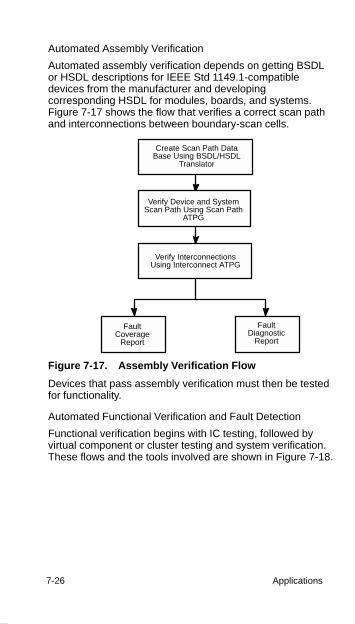
7-26 Applications
Automated Assembly Verification
Automated assembly verification depends on getting BSDLor HSDL descriptions for IEEE Std 1149.1-compatibledevices from the manufacturer and developingcorresponding HSDL for modules, boards, and systems.Figure 7-17 shows the flow that verifies a correct scan pathand interconnections between boundary-scan cells.
Create Scan Path DataBase Using BSDL/HSDL
Translator
Verify Device and SystemScan Path Using Scan Path
ATPG
Verify InterconnectionsUsing Interconnect ATPG
FaultCoverage
Report
FaultDiagnostic
Report
Figure 7-17. Assembly Verification Flow
Devices that pass assembly verification must then be testedfor functionality.
Automated Functional Verification and Fault Detection
Functional verification begins with IC testing, followed byvirtual component or cluster testing and system verification.These flows and the tools involved are shown in Figure 7-18.
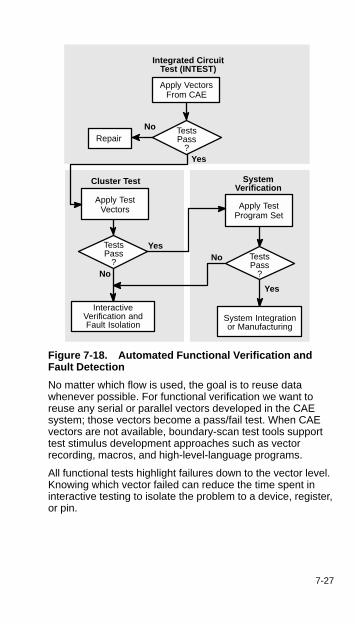
7-27
Integrated CircuitTest (INTEST)
Apply VectorsFrom CAE
TestsPass
?Yes
RepairNo
System Integrationor Manufacturing
Cluster Test
Apply TestVectors
SystemVerification
Apply TestProgram Set
TestsPass
?TestsPass
?
Yes
No
InteractiveVerification andFault Isolation
No
Yes
Figure 7-18. Automated Functional Verification andFault Detection
No matter which flow is used, the goal is to reuse datawhenever possible. For functional verification we want toreuse any serial or parallel vectors developed in the CAEsystem; those vectors become a pass/fail test. When CAEvectors are not available, boundary-scan test tools supporttest stimulus development approaches such as vectorrecording, macros, and high-level-language programs.
All functional tests highlight failures down to the vector level.Knowing which vector failed can reduce the time spent ininteractive testing to isolate the problem to a device, register,or pin.
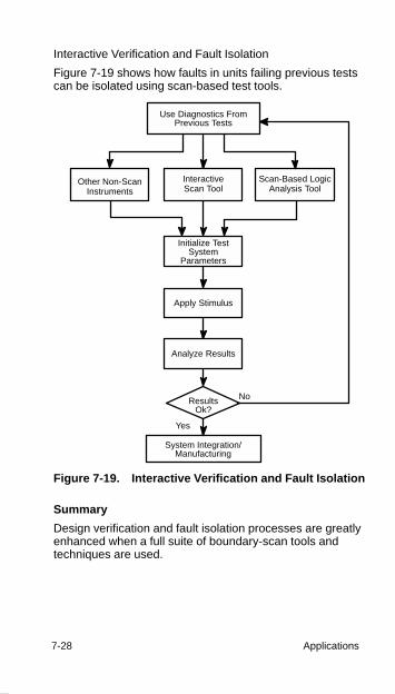
7-28 Applications
Interactive Verification and Fault Isolation
Figure 7-19 shows how faults in units failing previous testscan be isolated using scan-based test tools.
Scan-Based LogicAnalysis Tool
Use Diagnostics FromPrevious Tests
InteractiveScan Tool
Other Non-ScanInstruments
ResultsOk?
System Integration/Manufacturing
Initialize TestSystem
Parameters
Apply Stimulus
Analyze Results
Yes
No
Figure 7-19. Interactive Verification and Fault Isolation
Summary
Design verification and fault isolation processes are greatlyenhanced when a full suite of boundary-scan tools andtechniques are used.

8-1
Chapter 8Product Summary
This chapter provides a brief description of TI’scomprehensive offering of IEEE Std 1149.1-compatiblecomponents and a listing of TI’s IEEE Std 1149.1 (JTAG)boundary-scan logic product family.
IEEE Std 1149.1-Compatible Components
TI has a long history of involvement with JTAG and IEEE Std1149.1 and of support for integrated circuits that incorporateIEEE Std 1149.1-compatible boundary scan. Starting withrelease of the first commercially available boundary-scanlogic ICs in May 1990, only 3 months after ratification ofIEEE Std 1149.1, TI has lead the semiconductor industry inits offerings of products that support board- and system-leveltestability.
In addition to TI’s broad line of boundary-scan logic devices(see below), which are implemented primarily for the purposeof building board- and system-level test architectures, TIsupports IEEE Std 1149.1-compatible ICs across its broadproduct lines. From ASIC to DSP, networking to multimedia,TI’s portfolio includes many boundary-scan devices.
Highlights
ASIC — To facilitate the implementation of IEEE Std1149.1-compliant boundary scan in TI’s ASIC products,boundary-scan-cell modules have been developed for CMOSstandard-cell and gate-array libraries.
DSP — Select functions in TI’s ’C4x, ’C5x, ’C54x, and ’C8x(MVP) generations incorporate IEEE Std 1149.1 boundaryscan. In addition, all functions in these generations and in the’C2xx generation use the test access port (TAP), as specifiedby IEEE Std 1149.1, to access on-chip emulation features.
Networking — Currently, several functions fromThunderLAN (Ethernet ) and ThunderCELL(Asynchronous Transfer Mode) families offer IEEE Std1149.1 boundary scan.
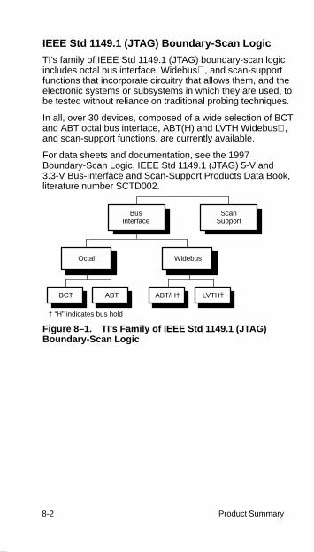
8-2 Product Summary
IEEE Std 1149.1 (JTAG) Boundary-Scan Logic
TI’s family of IEEE Std 1149.1 (JTAG) boundary-scan logicincludes octal bus interface, Widebus , and scan-supportfunctions that incorporate circuitry that allows them, and theelectronic systems or subsystems in which they are used, tobe tested without reliance on traditional probing techniques.
In all, over 30 devices, composed of a wide selection of BCTand ABT octal bus interface, ABT(H) and LVTH Widebus ,and scan-support functions, are currently available.
For data sheets and documentation, see the 1997Boundary-Scan Logic, IEEE Std 1149.1 (JTAG) 5-V and3.3-V Bus-Interface and Scan-Support Products Data Book,literature number SCTD002.
BusInterface
ScanSupport
Octal Widebus
ABTBCT
† “H” indicates bus hold
LVTH†ABT/H†
Figure 8–1. TI’s Family of IEEE Std 1149.1 (JTAG)Boundary-Scan Logic
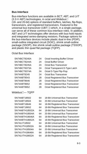
8-3
Bus Interface
Bus-interface functions are available in BCT, ABT, and LVT(3.3-V ABT) technologies, in octal and Widebus (18- and 20-bit) options of standard buffers, latches, flip-flops,transceivers, and registered transceivers. Featured is theuniversal bus transceiver (UBT ) which, in a single package,can serve all of these common bus-interface roles. In addition,ABT and LVT technologies offer devices with bus-hold inputsand integrated series-damping resistors. Package options forthe bus-interface devices include plastic dual in-line (PDIP),small-outline integrated circuit (SOIC), shrink small-outlinepackage (SSOP), thin shrink small-outline package (TSSOP),and plastic thin quad flat package (TQFP).
Octal Bus Interface
SN74BCT8240A 24 Octal Inverting Buffer/ DriverSN74BCT8244A 24 Octal Buffer/ DriverSN74BCT8245A 24 Octal Bus TransceiverSN74BCT8373A 24 Octal Transparent D-Type LatchSN74BCT8374A 24 Octal D-Type Flip-FlopSN74ABT8245 24 Octal Bus TransceiverSN74ABT8543 28 Octal Registered Bus TransceiverSN74ABT8646 28 Octal Registered Bus TransceiverSN74ABT8652 28 Octal Registered Bus TransceiverSN74ABT8952 28 Octal Registered Bus Transceiver
Widebus — TQFP
SN74ABT18502 64 18-Bit Universal Bus TransceiverSN74ABT18504 64 20-Bit Universal Bus TransceiverSN74ABT18646 64 18-Bit Registered Bus TransceiverSN74ABT18652 64 18-Bit Registered Bus TransceiverSN74ABTH18502A 64 18-Bit Universal Bus TransceiverSN74ABTH18504A 64 20-Bit Universal Bus TransceiverSN74ABTH18646A 64 18-Bit Registered Bus TransceiverSN74ABTH18652A 64 18-Bit Registered Bus TransceiverSN74LVT18502 64 18-Bit Universal Bus TransceiverSN74LVTH18502A 64 18-Bit Universal Bus TransceiverSN74LVTH18504A 64 20-Bit Universal Bus TransceiverSN74LVTH18646A 64 18-Bit Registered Bus TransceiverSN74LVTH18652A 64 18-Bit Registered Bus Transceiver
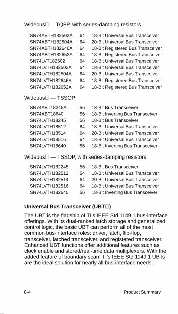
8-4 Product Summary
Widebus — TQFP, with series-damping resistors
SN74ABTH182502A 64 18-Bit Universal Bus TransceiverSN74ABTH182504A 64 20-Bit Universal Bus TransceiverSN74ABTH182646A 64 18-Bit Registered Bus TransceiverSN74ABTH182652A 64 18-Bit Registered Bus TransceiverSN74LVT182502 64 18-Bit Universal Bus TransceiverSN74LVTH182502A 64 18-Bit Universal Bus TransceiverSN74LVTH182504A 64 20-Bit Universal Bus TransceiverSN74LVTH182646A 64 18-Bit Registered Bus TransceiverSN74LVTH182652A 64 18-Bit Registered Bus Transceiver
Widebus — TSSOP
SN74ABT18245A 56 18-Bit Bus TransceiverSN74ABT18640 56 18-Bit Inverting Bus TransceiverSN74LVTH18245 56 18-Bit Bus TransceiverSN74LVTH18512 64 18-Bit Universal Bus TransceiverSN74LVTH18514 64 20-Bit Universal Bus TransceiverSN74LVTH18516 64 18-Bit Universal Bus TransceiverSN74LVTH18640 56 18-Bit Inverting Bus Transceiver
Widebus — TSSOP, with series-damping resistors
SN74LVTH182245 56 18-Bit Bus TransceiverSN74LVTH182512 64 18-Bit Universal Bus TransceiverSN74LVTH182514 64 20-Bit Universal Bus TransceiverSN74LVTH182516 64 18-Bit Universal Bus TransceiverSN74LVTH182640 56 18-Bit Inverting Bus Transceiver
Universal Bus Transceiver (UBT )
The UBT is the flagship of TI’s IEEE Std 1149.1 bus-interfaceofferings. With its dual-ranked latch storage and generalizedcontrol logic, the basic UBT can perform all of the mostcommon bus-interface roles: driver, latch, flip-flop,transceiver, latched transceiver, and registered transceiver.Enhanced UBT functions offer additional features such asclock enable and stored/real-time data multiplexers. With theadded feature of boundary scan, TI’s IEEE Std 1149.1 UBTsare the ideal solution for nearly all bus-interface needs.
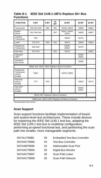
8-5
Table 8-1. IEEE Std 1149.1 UBTs Replace 50+ BusFunctions
FUNCTION 8 BIT 9 BIT 10BIT 16 BIT 18 BIT 20 BIT
Transceiver ’245,’623,’645 ’863 ’861 ’16245,’16623 ’16863 ’16861
Buffer/Driver ’241,’244,’541 ’827 ’16241,’16244,
’16541 ’16825 ’16827
LatchedTransceiver ’543 ’16543 ’16472
Latch ’373,’573 ’843 ’841 ’16373 ’16843 ’16841
RegisteredTransceiver ’646,’652 ’16646,
16652 ’16474
Flip-Flop ’374,’574 ’821 ’16374 ’16821
StandardUBT*
’16500,’16501
UniversalBus Driver ’16835
’18502 and ’18512 UBTs Replace Above Functions
RegisteredTransceiverw/CLKEnable
’2952 ’16470,’16952
Flip-Flopw/CLKEnable
’377 ’823 ’16823 ’16721
Std UBT*w/CLKEnable
’16600,16601
’18516 UBT Replaces Above Functions
’18504 and ’18514 UBTs Replace All Above Functions
*Non-Boundary-Scan Device
Scan Support
Scan-support functions facilitate implementation of board-and system-level test architectures. These include devicesfor mastering the IEEE Std 1149.1 test bus, adapting theIEEE Std 1149.1 test bus to multidrop configuration,performing at-speed functional test, and partitioning the scanpath into smaller, more manageable segments.
SN74LVT8980 28 Embedded Test-Bus Controller
SN74ACT8990 44 Test-Bus Controller
SN74ABT8996 24 Addressable Scan Port
SN74ACT8994 28 Digital Bus Monitor
SN74ACT8997 28 Scan-Path Linker
SN74ACT8999 28 Scan-Path Selector
8-6 Product Summary
Test-Bus Controllers
Embedded Test-Bus Controller (eTBC) — TheSN74LVT8980 provides a simple, off-the-shelf solution thatcan be hosted by a low-cost 8-bit microcontroller ormicroprocessor to generate the signals required to masterthe IEEE Std 1149.1 test bus. Its LVT implementation meansthat this device is the industry’s first test-bus solution tooperate at 3.3 V, while it still interfaces to scan-path devicesthat use 5-V power.
Test-Bus Controller (TBC) — The SN74ACT8990 provides asimple, off-the-shelf solution that can be hosted by a 16-bitmicrocontroller/microprocessor to generate the signalsrequired to master the IEEE Std 1149.1 test bus.
Backplane/Multidrop Test-Bus Support
Addressable Scan Port (ASP) — IEEE Std 1149.1 defineshow to implement boundary scan at the IC level but does notaddress board- or system-level architectures. With TI’sSN74ABT8996 device, backplane or other multidropapplications now can be supported.
At-Speed Functional Test
Digital Bus Monitor (DBM) — The SN74ACT8994 is aspecial-function device that provides the capability toemulate the functions of logic and signal analyzers. TheDBM can be embedded in systems as a non-intrusiveat-speed monitor. A single DBM monitors up to 16 signals,but several can be used in concert for width or depthexpansion.
Scan-Path Support
Scan-Path Linker (SPL) — The SN74ACT8997 provides forscan-path partitioning by allowing selection, under IEEE Std1149.1 scan control, of any combination of up to foursecondary scan paths. Multiple SPL devices can becascaded to support any desired number of secondary scanpaths, as well as multilevel hierarchies.
Scan-Path Selector (SPS) — The SN74ACT8999 providesfor scan-path partitioning by allowing selection, under IEEEStd 1149.1 scan control, of any one of four secondary scanpaths.

8-7
Not all devices mentioned are available at the time ofthis printing. Contact your TI sales representative orauthorized distributor for commercial or military gradeavailability information.
Note:
9-1
Chapter 9Other Support and Learning Products
This chapter provides information concerning learning toolsavailable for IEEE Std 1149.1-1990.
Scan Educator
The Scan Educator PC-based tutorial software introducesthe fundamentals of IEEE Std 1149.1, including architecture,protocols, and required instruction set. Self-paced andmenu-driven, it contains both information and animatedboundary-scan simulations. Hands-on exercises guide youthrough a boundary-scan test of an IEEE Std1149.1-compliant octal at the bit-by-bit and register levels.You also are shown how to use boundary-scan testing withsingle or multiple devices for in-circuit observability andcontrollability.
Scan Board
No matter where you are on the boundary-scan learningcurve, TI’s Scan Board can help you move to higher levels ofunderstanding — quickly and easily. Scan Board can be alearning tool for new users of boundary-scan and a test andevaluation platform for the experienced user. This speciallydeveloped board comes with multiple IEEE Std1149.1-compliant devices that can help you evaluate both thetools and the concepts behind board-level testing. With ScanBoard, you can perform boundary-scan interconnect testsand insert various faults and fault types, as well asdemonstrate board-level built-in self-test (BIST) for testingmemory, internal test (INTEST) of an ASIC, internal BIST ofan ASIC, cluster testing, single- and multiple-scan paths, andmany other capabilities. Scan Board comes with schematics,netlists, X-Y plots, data sheets, test patterns, BSDLdescriptions, and a free executable software program. Thissoftware allows you to apply test patterns supplied with ScanBoard, or to apply your own.

9-2 Other Support and Learning Products
Scan Board demonstrates these advanced test techniquesand more:
Scan-path verification
Interconnect testing
Pins-in (IC core logic) testing
BIST methods at the device and board level
Boundary-scan interconnect automatic test-patterngeneration (ATPG)
Functional cluster logic tests using boundary-scan andBIST capabilities
Fault detection and isolation
Control and monitoring of discrete event lines
Counting, toggle, and pseudorandom pattern generation(PRPG) stimulus methods
Parallel signature analysis (PSA) response capture
Scan-path switching
Flexibility
Scan Board incorporates basic boundary-scan features fornew users to learn boundary-scan testing, and alsoincorporates advanced extensions such as BIST, INTEST,internal scan, and multiple scan paths for advanced users.Scan Board’s physical layout separates independent multiplefunctions both electrically and physically, while maintaining asingle continuous IEEE Std 1149.1 scan path for ease of testmanipulation. Fault-injection switches are provided so theuser can practice fault-isolation techniques. Scan Boardprovides for the injection of 12 different faults. Fault typesinclude: stuck-at-one, stuck-at-zero, bridging, non-adjacentbridging, internal device, and scan path.
9-3
Compatibility
Scan Board is compatible with in-circuit test fixtures andtesters. Nodes are accessible via boundary-scan or from thebottom with adequate and uniform spacing for in-circuitprobes. Nets without both the boundary-scan driver andreceiver are accessible via 40-mil probe points with 100-milspacing.
Supporting Documentation Included
Scan Board comes with board description and operation,schematics and diagrams, X-Y and Gerber plots, a faulttable, and boundary-scan device data sheets. Electronic filesinclude BSDL, HSDL, Netlists (Viewlogic, EDIF 2.0.0, andTeradyne CDB), interconnect patterns (SVF), ASIC internaltest patterns (SVF), and cluster-logic test patterns (SVF).Scan Board demonstration software is included at no extracharge.
CD-ROM
TI has combined the key elements of IEEE Std 1149.1 on asingle CD-ROM. Now the latest versions of the IEEE Std1149.1-1990 (including IEEE Std 1149.1a-1993) are mergedinto one searchable document.
Also included are TI’s:
Test-bus evaluation report
Application notes
Data sheets for TI boundary-scan products
The test-bus evaluation (TBE) report was written by TI’sDefense Systems & Electronics Group to evaluate theapplications and impact of standard test buses on overallsystem testability. The TBE report is based on years oftest-bus development and applications experience at TI;since the early 1980s, TI has played a key role in definingtest buses, first, for the VHSIC program, and then later as akey contributor in both JTAG and IEEE Std 1149.1.
This CD-ROM brings together current information on IEEEStd 1149.1. Microsoft and UNIX environments are supported.
9-4 Other Support and Learning Products
Testability Video Tape
Texas Instruments offers a 74-minute, two-part video toexplain the concept of testability. The tapes are available inU.S. (NTSC) and international (PAL) formats.
Tape 1 — The first tape explains the growing importance oftestability and the tremendous potential impact on cost,time, and quality that design for test (DFT) can have. Italso describes the work of the Joint Test Action Group(JTAG) and the provisions of IEEE Std 1149.1.
Tape 2 — The second tape examines the standard in moredetail. It explains the test-bus architecture andinstructions and shows how to use boundary-scantesting on a board or system. The tape includessoftware-support standards, example application, andinformation on how boundary-scan test tools helpautomate boundary-scan testing. The tape clearlyexplains the function of each component of thestandard, and shows how they work together to providean accurate, dependable test procedure.
Boundary-Scan Video Outline
Introduction — Testing problems and concepts
Economics — Benefits and cost-reduction potential
Design-for-Testability Concept — Controls, diagnosis,DFT strategies, and more
Introduction — IEEE Std 1149.1 Boundary Scan
Details of IEEE Std 1149.1
Testing With IEEE Std 1149.1 Boundary Scan — Duringdesign and development, production, field testing andmaintenance. Also in this section: testing theboundary-scan core logic at the board level, optimizedinterconnect tests, isolating interconnect faults, testingboards with a mix of boundary-scan andnonboundary-scan components, testing mixed-signalboards, and exploiting BIST during tests.
Digital Applications of IEEE Std 1149.1 Boundary Scan— Data formats supporting boundary scan, plusapplication notes
9-5
Proposed Product Development and Support Cycle
Commercially Available Products for DFT
Available Training on DFT and Boundary Scan
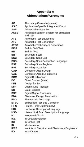
A-1
Appendix AAbbreviations/Acronyms
AC Alternating Current (dynamic)ASIC Application-Specific Integrated CircuitASP Addressable Scan PortASSET Advanced Support System for Emulation
and TestATE Automatic Test EquipmentATG Automatic Test GenerationATPG Automatic Test-Pattern GenerationBIST Built-In Self-TestBIT Built-In TestB/S Boundary ScanBSC Boundary-Scan CellBSDL Boundary-Scan Description LanguageBSR Boundary-Scan RegisterBST Boundary-Scan TestCAD Computer-Aided DesignCAE Computer-Aided EngineeringDBM Digital Bus MonitorDC Direct Current (static)DFT Design for TestDIP Dual In-Line PackageDR Data RegisterDSP Digital Signal ProcessorEDA Electronic Design AutomationESD Electrostatic DischargeETBC Embedded Test-Bus ControllerFIFO First-In, First-Out (memory)HDL Hardware Description LanguageHSDL Hierarchical Scan Description LanguageIC Integrated CircuitICE In-Circuit EmulationICT In-Circuit TestID IdentificationIEEE Institute of Electrical and Electronics EngineersI/O Input/Output
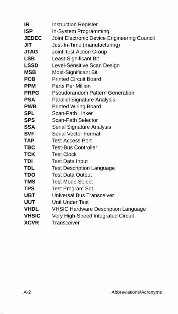
A-2 Abbreviations/Acronyms
IR Instruction RegisterISP In-System ProgrammingJEDEC Joint Electronic Device Engineering CouncilJIT Just-In-Time (manufacturing)JTAG Joint Test Action GroupLSB Least-Significant BitLSSD Level-Sensitive Scan DesignMSB Most-Significant BitPCB Printed Circuit BoardPPM Parts Per MillionPRPG Pseudorandom Pattern GenerationPSA Parallel Signature AnalysisPWB Printed Wiring BoardSPL Scan-Path LinkerSPS Scan-Path SelectorSSA Serial Signature AnalysisSVF Serial Vector FormatTAP Test Access PortTBC Test-Bus ControllerTCK Test ClockTDI Test Data InputTDL Test Description LanguageTDO Test Data OutputTMS Test Mode SelectTPS Test Program SetUBT Universal Bus TransceiverUUT Unit Under TestVHDL VHSIC Hardware Description LanguageVHSIC Very High-Speed Integrated CircuitXCVR Transceiver
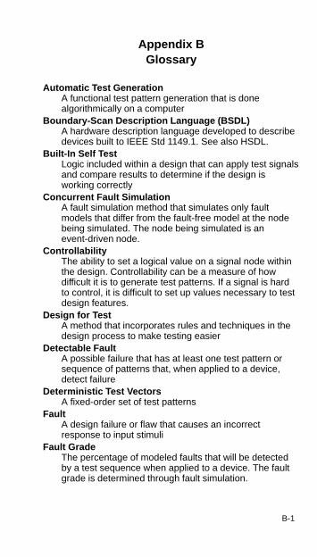
B-1
Appendix BGlossary
Automatic Test GenerationA functional test pattern generation that is donealgorithmically on a computer
Boundary-Scan Description Language (BSDL)A hardware description language developed to describedevices built to IEEE Std 1149.1. See also HSDL.
Built-In Self TestLogic included within a design that can apply test signalsand compare results to determine if the design isworking correctly
Concurrent Fault SimulationA fault simulation method that simulates only faultmodels that differ from the fault-free model at the nodebeing simulated. The node being simulated is anevent-driven node.
ControllabilityThe ability to set a logical value on a signal node withinthe design. Controllability can be a measure of howdifficult it is to generate test patterns. If a signal is hardto control, it is difficult to set up values necessary to testdesign features.
Design for TestA method that incorporates rules and techniques in thedesign process to make testing easier
Detectable FaultA possible failure that has at least one test pattern orsequence of patterns that, when applied to a device,detect failure
Deterministic Test VectorsA fixed-order set of test patterns
FaultA design failure or flaw that causes an incorrectresponse to input stimuli
Fault GradeThe percentage of modeled faults that will be detectedby a test sequence when applied to a device. The faultgrade is determined through fault simulation.
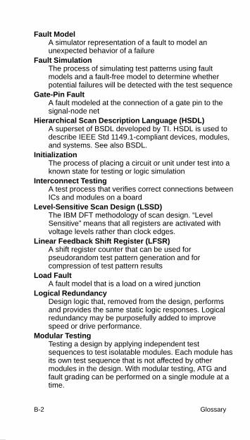
B-2 Glossary
Fault ModelA simulator representation of a fault to model anunexpected behavior of a failure
Fault SimulationThe process of simulating test patterns using faultmodels and a fault-free model to determine whetherpotential failures will be detected with the test sequence
Gate-Pin FaultA fault modeled at the connection of a gate pin to thesignal-node net
Hierarchical Scan Description Language (HSDL)A superset of BSDL developed by TI. HSDL is used todescribe IEEE Std 1149.1-compliant devices, modules,and systems. See also BSDL.
InitializationThe process of placing a circuit or unit under test into aknown state for testing or logic simulation
Interconnect TestingA test process that verifies correct connections betweenICs and modules on a board
Level-Sensitive Scan Design (LSSD)The IBM DFT methodology of scan design. “LevelSensitive” means that all registers are activated withvoltage levels rather than clock edges.
Linear Feedback Shift Register (LFSR)A shift register counter that can be used forpseudorandom test pattern generation and forcompression of test pattern results
Load FaultA fault model that is a load on a wired junction
Logical RedundancyDesign logic that, removed from the design, performsand provides the same static logic responses. Logicalredundancy may be purposefully added to improvespeed or drive performance.
Modular TestingTesting a design by applying independent testsequences to test isolatable modules. Each module hasits own test sequence that is not affected by othermodules in the design. With modular testing, ATG andfault grading can be performed on a single module at atime.
B-3
Multiple FaultA fault model created by simultaneously representingthe fault with multiple stuck-at faults
Node FaultA fault model that ties an interconnection net to a fixedlogic level. A node fault is equivalent to all sources on anet being source faults with the same logical value.
ObservabilityThe capability to observe the effect of a node value at anoutput pin. If the node value changes, the output valuealso changes.
Parallel Fault SimulationA method that simulates a set of fault models at thesame time as the fault-free model
Parallel Signature AnalyzerAn LFSR used to compress test data by collecting datafrom the design and exclusive ORing the resulting testdata with register-state data
Parametric TestA test that checks the voltage, current, and timingspecifications of a design. The ac and dc propagationtests are parametric tests.
PropagationThe response of an output of a gate (or net) to an inputof the gate (or net)
Scan-Path DesignA DFT methodology where all or a selected group ofstorage elements can be serially interconnected tofacilitate testing of embedded combinational logic in anintegrated circuit
Scan-Path Linker (SPL)TI’s SN74ACT8997 device acts as a scan-pathmultiplexer, allowing dynamic path switching. The SPLcan select any combination of four secondary scanpaths.
Scan-Path Selector (SPS)TI’s SN74ACT8999 device acts as a scan-pathmultiplexer, allowing dynamic path switching. The SPScan select one of four secondary scan paths at a time.
B-4 Glossary
Scan TestingThe DFT technique that connects all internal registers ina design into a shift register used during test. The scanshift registers, called scan paths, are used to load anydesirable state before application of a test overcombinational logic between serial (scannable) registerlatches and unload any resultant state for observation.
Serial Vector Format (SVF)A standard ASCII-based pattern format for expressingIEEE Std 1149.1 scan operations and state transitions.This vector format was jointly developed by TI andTeradyne to allow pattern transportability between testtools.
Source FaultA fault model that is a source to a wired-junction net.Gate outputs are examples of source faults.
Stuck Closed (Shorted Gate) FaultA stuck-at fault model in which the transistor controlledby the gate is always closed. This has the same effectas shorted data lines. This fault model is the same as anSA1 fault on the gate input of an n-p-n transistor or anSA0 fault on the gate input of a p-n-p transistor.
Stuck FaultA failure model in which a gate pin is modeled as stuckto VCC (for stuck-at-one, SA1 ) or to GND (forstuck-at-zero, SA0)
Stuck Open (Open Gate) FaultA stuck-fault model in which the transistor controlled bythe gate is always open. This fault model is the same asan SA0 fault on the gate input of an n-p-n transistor oran SA1 fault on the gate input of a p-n-p transistor.
Test Access Port (TAP)Port described in IEEE Std 1149.1-1990. Must contain aminimum of three input connections (TDI, TMS, TCK)and one output connection (TDO). A fourth inputconnection (TRST*) is optional. The TAP providesaccess to test functions built into a component.
Test Description Language (TDL)A test pattern format that describes the stimuli andexpected results for a test application. TDL tests areapplied using I/O connector pins.
B-5
Test GenerationThe process of producing a test sequence to test adesign. Three methods of test generation are: automatictest generation (ATG), manual test preparation, andrandom input values generation.
Test PatternA set of input stimuli values that are applied at thebeginning of a period of time and a set of outputobservation values made at the end of a period of timethat are represented by a string of values
Test Pattern GradingThe process of fault simulating a test pattern sequenceto obtain a fault grade
Test Point InsertionThe DFT technique that includes additional connectionsto internal nodes for either control or state observation
Test VectorAnother name for a test pattern
TestabilityThe property of a circuit, board, or system that enablestesting
Undetectable FaultA fault that cannot be detected by any achievable testpattern. Undetectability may be due to logic redundancyor to logic that cannot be observed.
Unpredictable FaultA fault that causes the value of a node to beindeterminate, thereby making it impossible to detect afault

C-1
Appendix CReferences
1. Agrawal, Vishwani D., “Sampling Techniques forDetermining Fault Coverage in LSI Circuits,” Journal ofDigital Systems, Vol. V., Number 3, pp. 189-203.
2. Bennetts, R. G., Introduction to Digital Board Testing,Crane, Russak & Company, Inc., NY, NY, 1982.
3. Bhavsar, D. K., and R. W. Heckelman, “Self-Testing byPolynomial Division,” Digest of IEEE TestConferences,1981, pp. 208-216.
4. Bleeker, van den Eijnden, de Jong, Boundary-Scan Test— A Practical Approach, ISBN 0-792-9296-5.
5. Frohwerk, R. A., “Signature Analysis: A New Digital FieldService Method,” Hewlett-Packard Journal, May 1977,pp. 2-8.
6. IEEE Std 1149.1-1990 (includes IEEE Std 1149.1a-1993),IEEE Standard Test Access Port and Boundary-ScanArchitecture, ISBN 1-55937-350-4.
7. IEEE Std 1149.1b-1994, Supplement to IEEE StandardTest Access Port and Boundary-Scan Architecture, ISBN1-55937-497-7.
8. Jandhyala, S. and A.W. Ley, “Design-for-Test Analysis ofa Buffered SDRAM DIMM,” 1996 Proceedings,International Workshop on Memory Technology, Design,and Testing.
9. Ley, A. W., “A Look at Boundary Scan from a Designer’sPerspective,” 1994 Proceedings, Electronic Design,Automation & Test Asia Conference.
10.Maunder, Colin M. and Rodham E. Tulloss, The TestAccess Port and Boundary-Scan Architecture, ISBN0-8186-9070-4.
C-2 References
11. Parker, Kenneth P., The Boundary-Scan Handbook, ISBN0-7923-9270-1.
12.Peterson, W. W., and E. J. Weldon Jr., Error CorrectingCodes, MIT Press, Cambridge, MA, 1972.
13.Pynn, C., Strategies for Electronics Test, McGraw-Hill,Inc., NY, 1986.
14.Sridhar, T., D. S. Ho, T. J. Powell, and S. M. Thatte,“Analysis and Simulation of Parallel Signature Analyzers,”1982 International Test Conference, Philadelphia, PA,November 15-18,1982, pp. 656-661.
15.Thatte, S. M., D. S. Ho, H. T. Yuan, T. Sridhar, and T. J.Powell, “An Architecture for Testable VLSI Processors,”1982 International Test Conference, Philadelphia, PA,November 15-18, 1982, pp. 484-493.
16.Turner, M.E., D. G. Leet, Ronald J. Prilik, and D. J.McLean, “Testing CMOS VLSI: Tools, Concepts, andExperimental Results,” 1985 International TestConference, Philadelphia, PA, November 19-21, 1985,pp. 322-328.
17.Whetsel, L., “A Proposed Standard Test Bus andBoundary Scan Architecture,” 1988 IEEE InternationalConference on Computer Design, Rye Brook, NY,October 3-5, 1988, pp. 330-333.
18.Whetsel, L., “A Proposed Method of Accessing 1149.1 inBackplane Environment,” 1992 Proceedings, InternationalTest Conference.
19.Whetsel, L., “Hierarchically Accessing 1149.1Applications in a System Environment,” 1993Proceedings, International Test Conference.
20.Williams, T. W., “VLSI Testing,” Computers, Vol. 17, No.10, October 1984, pp. 126-136.
D-1
Appendix DInternet Starting Points
Institute of Electrical and Electronics Engineers (IEEE)http://www.ieee.org/index.html
IEEE Std 1149.1http://www.computer.org/tab/tttc/standard/s1149-1/home.html
Test Technology Technical Committee (sponsor for IEEE1149.x standards)
http://www.computer.org/tab/tttc/
Texas Instrumentshttp://www.ti.com
Texas Instruments Semiconductor Grouphttp://www.ti.com/sc/docs/schome.htm
Texas Instruments Advanced System Logichttp://www.ti.com/sc/docs/asl/home.htm
Texas Instruments IEEE 1149.1 (JTAG) Boundary Scanhttp://www.ti.com/sc/docs/jtag/jtaghome.htm
Texas Instruments IEEE 1149.1 Silicon Product and BSDLAvailabilityhttp://www.ti.com/sc/docs/jtag/silicon.htm
Texas Instruments Product Information Data Sheet Searchhttp://www.ti.com/sc/docs/psheets/pids.htm
Index-1
Index
AABT octals, 8-2, 8-3
ABT Widebus, 8-2, 8-3, 8-4
Addressable Scan Port(ASP), 8-6
application illustrated, 7-20introduction, 7-19
application notes, 9-3
ASIC, 8-1
ASP. See Addressable ScanPort
at-speed functional test, 8-6
automatic test equipment(ATE)
board-etch and solder-jointtesting, 7-1
traditional test, 2-1use of BSDL, 5-1use of SVF, 5-9, 6-6
automatic test generation(ATG), defined, B-1
automatic test-patterngeneration (ATPG)
BSDL input, 5-1impact on time to market,
4-3in assembly verification
flow, 7-26SVF output, 6-6, 6-9
Bbackplane configuration
multidrop (ASP), 7-19, 8-6illustrated, 7-20
ring, 7-17illustrated, 7-18
star, 7-18illustrated, 7-19
backplane faults, 7-7, 7-8,7-9
BCT octals, 8-2, 8-3
board designflow illustrated, 6-4principles discussed, 6-8
board faults, 1-4
boundary-scan, See alsoIEEE Std 1149.1
ASIC synthesis, 6-4ASIC testability, 4-9ASIC verification, 7-10automated assembly
verification, 7-26automated functional
verification, 7-25backplane multidrop
testing, 7-17, 8-6illustrated, 7-20
benefits, 1-5, 2-1, 2-2, 3-1,3-2
board testing, 1-4, 7-1board validation, 6-9CD-ROM, 9-3
Index-2
boundary-scan (continued)circuit partitioning
described, 2-2illustrated, 2-3
cluster testing, 7-5constraints, 6-8controllability and
observability, 3-2described, 3-1design considerations
illustrated, 6-1design debug and
verification illustrated,6-7
design flow illustrated, 6-4edge connector testing, 7-7embedded testing, 7-21evaluation, 9-1illustrated, 3-2in surface-mount devices,
3-1interactive verification,
7-28interconnect testing, 3-1,
3-2manufacturing test, 6-9memory test times, table,
7-14memory testing, 7-12microcode simulation, 7-11signature analysis, 7-6test development, 7-10test flow, 7-24testing,
design overview, 6-1illustrated, 2-3
tutorial (Scan Educator),9-1
vector processorverification, 7-10
video tape, 9-4
boundary-scan cell (BSC)described, 3-2illustrated, 3-11
Boundary-Scan DescriptionLanguage (BSDL)
boundary registerdescription, 5-4
component conformancestatement, 5-3
defined, B-1elements of, 5-2entity descriptions, 5-2error types, 5-5for ASICs, 6-5for catalog devices, 5-5generic parameter, 5-3history, 5-1instruction register
description, 5-3logical port description, 5-3optional register
description, 5-4pin mapping, 5-3register access
description, 5-4scan port identification, 5-3subset of VHDL syntax,
5-1use statements, 5-3uses, 5-1validation, 5-4, 6-7
Index-3
boundary-scan register(BSR)
described, 3-10illustrated, 3-4in BSDL, 5-4in use
CLAMP, 3-13EXTEST, 3-14INTEST, 3-13SAMPLE/PRELOAD,
3-12
built-in self-test (BIST)defined, B-1in ASICs, 4-9initiated by IEEE Std
1149.1, 3-13, 6-3, 7-13test functions, 6-3
bus interface, 8-3
bypass registerdescribed, 3-11in use
BYPASS, 3-12CLAMP, 3-13default, 3-9HIGHZ, 3-14
CCD-ROM with IEEE Std
1149.1, 9-3
concurrent fault simulation,defined, B-1
controllability, 3-2, 6-2, 7-11defined, B-1in embedded memory,
7-12
cost of testing, 1-3, 2-1
Ddata sheets, for TI IEEE Std
1149.1 testabilitydevices, 9-3
DBM. See Digital BusMonitor
design for testadditional cost amortized,
2-1ASIC
fault simulation, 4-1testability, 4-1
circuit isolation, 2-2concerns, 6-1cost of overlooked defects,
4-7illustrated, 4-8
cycle-time reduction, 4-3defined, 1-1, B-1design constraints, 4-2design costs, 1-4design flow
described, 6-1illustrated, 6-1, 6-4, 6-7
design impact, 1-4, 4-2developing test strategies,
4-8economic trade-off, 4-4effect on hardware, 4-1embedded test, 2-1improved debugging, 4-4in ASICs, 4-1in the design process, 4-1introduction to, 1-1new tool costs, 4-7
Index-4
design for test (continued)partitioning penalties, 6-9rationale, 1-2reduced cost and higher
quality, 1-3reduced manufacturing
cost, 2-2standard test approach,
2-2strategy, 4-3system-level approach, 1-3test strategy flow
illustrated, 4-11test strategy vs. gate
density, 4-9with ATPG, 4-4yield vs. devices/board, 4-6yield vs. fault grade, 4-5
detectable fault, defined, B-1
deterministic test vectors,defined, B-1
device identification registerdescribed, 3-11illustrated, 3-11in BSDL, 5-4in use
default, 3-9IDCODE, 3-14USERCODE, 3-14
Digital Bus Monitor (DBM),8-6
DSP, 8-1
EEmbedded Test-Bus
Controller, (eTBC), 7-21,8-6
Ffault, defined, B-1
fault gradedefined, B-1simulator results, 4-1
fault modeldefined, B-2examples, 4-1
fault simulationdefined, B-2in ASIC design, 4-1
Ggate-pin fault, defined, B-2
Index-5
HHierarchical Scan
Description Language(HSDL), See alsoBoundary-ScanDescription Language
bus composition, 5-8defined, B-2described, 5-6elements of, 5-6entity description, 5-7generic parameter, 5-7history, 5-6logical port description, 5-7members description, 5-8obtaining specifications,
5-8path descriptions, 5-8pin mapping, 5-7scan port identification, 5-8use statements, 5-7uses, 5-6, 6-8
IIC test, explained, 6-6
IEEE Std 1149.1, See alsoboundary scan,Boundary-ScanDescription Language
architecturedescribed, 3-3illustrated, 3-4
benefits, 6-10built-in self-test, 6-3bus master. See Test Bus
Controller
IEEE Std 1149.1 (continued)internal scan, 6-3introduction, 1-5macro libraries, 6-5obtaining specifications,
3-15on CD-ROM, 9-3optional pins, B-4
TRST*, 3-14optional registers, 3-9
device identificationregister, 3-11
user-defined dataregister, 3-9
optional test instructionsCLAMP, 3-13HIGHZ, 3-14IDCODE, 3-14INTEST, 3-13RUNBIST, 3-13USERCODE, 3-14
origins of, 3-1partitioned scan path, 6-8,
8-6required pins, 1-5, B-4
TCK, 3-5TDI, 3-5TDO, 3-5TMS, 3-5
required registersboundary-scan register,
3-10bypass register, 3-11instruction register, 3-8
required test instructionsBYPASS, 3-12EXTEST, 3-13SAMPLE/PRELOAD,
3-12reuse of test vectors, 3-1,
6-10
Index-6
IEEE Std 1149.1 (continued)supporting data formats,
5-1test data registers
described, 3-9illustrated, 3-10
IEEE Std 1149.1-compatiblecomponents, 8-1
IEEE Std 1149.1 (JTAG)Boundary-Scan Logic,8-2
bus interface, 8-3scan support, 8-5Universal Bus Transceiver
(UBT), 8-4
in-circuit test, described, 7-1
initialization, defined, B-2
instruction registerdescribed, 3-8illustrated, 3-8in BSDL, 5-3
interconnect testing, 6-2, 6-5,6-9, 7-1
defined, B-2described, 3-2illustrated, 7-2
internal scan, described, 6-3
JJoint Test Action Group
(JTAG), See alsoboundary scan, IEEE Std1149.1
Joint Test Action Group(continued)
introduction, 1-5
Llevel-sensitive scan design
(LSSD)defined, B-2in ASICs, 4-10
linear feedback shift register(LFSR), defined, B-2
load fault, defined, B-2
logical redundancy, defined,B-2
LVT Widebus, 8-2, 8-3, 8-4
Mmemory test
controllability, 7-12embedded memory, 7-12observability, 7-12
modular testing, defined, B-2
multidrop test bus, 7-19,7-20, 8-6
multiple fault, defined, B-3
Index-7
Nnetworking ICs, 8-1
node fault, defined, B-3
Oobservability, 3-2, 6-2, 7-11
defined, B-3in embedded memory,
7-12
octals, bus interface, 8-3
Pparallel fault simulation,
defined, B-3
parallel signature analyzer,defined, B-3
parametric test, defined, B-3
product summary, 8-1
propagation, defined, B-3
SScan Board, 9-1
Scan Educator tutorial, 9-1
Scan Engine, 7-21
scan pathdescribed, 3-2illustrated, 3-2
scan-path design, defined,B-3
Scan-Path Linker (SPL), 8-6defined, B-3
scan-path partitioning, 6-8,8-6
Scan-Path Selector (SPS),8-6
defined, B-3
scan testing, defined, B-4
Serial Vector Format (SVF)defined, B-4described, 5-9headers and trailers
illustrated, 5-10history, 5-9obtaining specifications,
5-16offset commands, 5-11parallel commands, 5-12program example, 5-15scan offsets, 5-9state commands, 5-11structure, 5-10TAP state names, table,
5-13uses, 5-9
SN74ABT8996 (ASP), Seealso Addressable ScanPort, 7-19, 8-6

Index-8
SN74ACT8990 (TBC), Seealso Test-Bus Controller,7-21, 8-6
SN74ACT8994 (DBM), Seealso Digital Bus Monitor,8-6
SN74ACT8997 (SPL), Seealso Scan-Path Linker,6-8, 8-6
SN74ACT8999 (SPS), Seealso Scan-Path Selector,8-6
SN74LVT8980 (eTBC), Seealso Embedded Test-BusController, 7-21, 8-6
source fault, defined, B-4
SPL. See Scan-Path Linker
SPS. See Scan-PathSelector
stuck closed (shorted gate)fault, defined, B-4
stuck fault, defined B-4
stuck open (open gate) fault,defined, B-4
TTBC. See Test-Bus
Controller
testapplications
ASIC verification, 7-10backplane multidrop
testing, 7-17board etch/solder joint
testing, 7-1boundary-scan test flow,
7-24cluster testing, 7-5edge connector testing,
7-7embedded testing, 7-21memory testing, 7-12
costs of traditional ATE,2-1
design validation, 6-6fault isolation, 6-6fault simulation and
grading, 4-1functional, at-speed, 8-6IC simulation, 6-6product test requirements,
6-2reduced manufacturing
cost, 2-2reusing vectors, 6-10traditional ATE
bare board test, 7-1in-circuit test, 7-1
Index-9
test access port (TAP)controller state diagram
illustrated, 3-5defined, B-4described, 3-3detailed description, 3-6in BSDL, 5-3operation, 3-5output control illustrated,
3-7
Test-Bus Controller (TBC),7-17, 7-21, 8-6
test-bus evaluation report,9-3
test-bus master. SeeTest-Bus Controller
test data registers illustrated,3-10
test description language(TDL), defined, B-4
test generation, defined, B-5
test pattern, defined, B-5
test pattern grading, defined,B-5
test point insertion, defined,B-5
test program, developmenttime required, table, 1-4
test vector, defined, B-5
testability, See also designfor test
defined, 1-1, B-5
testability video, 9-4
time to marketimpact on profitability, 1-3introduction, 4-3relationship to testability,
4-4illustrated, 4-3
training productsCD-ROM, 9-3Scan Board, 9-1Scan Educator, 9-1testability video, 9-4
tutorial (Scan Educator), 9-1
Uundetectable fault, defined,
B-5
Universal Bus Transceiver(UBT), 8-4
unpredictable fault, defined,B-5
Vvideo tape on testability, 9-4
WWidebus, 8-2, 8-3, 8-4