JTAG Programmer Overview for Hercules-Based Microcontrollers · JTAG Programmer Overview for...
24
Application Report SPNA230 – November 2015 JTAG Programmer Overview for Hercules-Based Microcontrollers Charles Tsai ABSTRACT This application report describes the necessary steps needed by the third party developers to create a JTAG-based flash programmer for the Hercules™ family of microcontrollers. This document does not substitute the existing user guides on JTAG access to the target systems and how to program the Flash memory, but rather serves as a central location to reference these documents with clarifications specific to the implementation of the Hercules family of microcontrollers. Contents 1 Introduction ................................................................................................................... 2 2 Hercules JTAG Scan Architecture ......................................................................................... 2 3 Creating the Firmware to Program the Flash Memory ................................................................ 22 4 Flash Verification ........................................................................................................... 23 5 References .................................................................................................................. 23 List of Figures 1 Hercules JTAG Scan Architecture ......................................................................................... 3 2 Conceptual ICEPICK-C Block Diagram for Hercules Implementation ................................................ 5 3 Fields of the 32-Bit Scan Value for Accessing Mapped Registers .................................................... 6 4 Hercules JTAG Scan After DAP is Selected ............................................................................. 9 5 CCS View of the ICEPick Router ........................................................................................ 10 6 Structure of the DAP Components and Its Interfaces to the System................................................ 11 7 Accessing CoreSight Components Using APB-AP Interface ......................................................... 12 8 Accessing CoreSight ETM Using APB Mux Interface ................................................................. 12 9 Accessing System Memories Using AHB-AP Interface ............................................................... 13 10 Accessing Peripheral Using AHB-AP Interface......................................................................... 13 11 Accessing System Memories Using APB-AP Interface ............................................................... 14 12 JTAG-DP and AHB-AP Interface to the System Resources.......................................................... 15 13 JTAG-DP and APB-AP Interface to the System Resources Via the Processor.................................... 19 14 FirmWare Update .......................................................................................................... 22 List of Tables 1 Instructions Accepted by the ICEPick TAP ............................................................................... 4 2 Debug Connect Register (DCON) Field Descriptions .................................................................. 4 3 Mapped Register Selection ................................................................................................. 6 4 AHB-AP and APB-AB Availabilities in Hercules Devices ............................................................ 11 5 Cortex-Rx Debug Memory-Mapped Registers ......................................................................... 20 Hercules, Code Composer Studio are trademarks of Texas Instruments. All other trademarks are the property of their respective owners. 1 SPNA230 – November 2015 JTAG Programmer Overview for Hercules-Based Microcontrollers Submit Documentation Feedback Copyright © 2015, Texas Instruments Incorporated
-
Upload
nguyencong -
Category
Documents
-
view
261 -
download
0
Transcript of JTAG Programmer Overview for Hercules-Based Microcontrollers · JTAG Programmer Overview for...
Application ReportSPNA230–November 2015
JTAG Programmer Overview for Hercules-BasedMicrocontrollers
CharlesTsai
ABSTRACTThis application report describes the necessary steps needed by the third party developers to create aJTAG-based flash programmer for the Hercules™ family of microcontrollers. This document does notsubstitute the existing user guides on JTAG access to the target systems and how to program the Flashmemory, but rather serves as a central location to reference these documents with clarifications specific tothe implementation of the Hercules family of microcontrollers.
Contents1 Introduction ................................................................................................................... 22 Hercules JTAG Scan Architecture......................................................................................... 23 Creating the Firmware to Program the Flash Memory ................................................................ 224 Flash Verification ........................................................................................................... 235 References .................................................................................................................. 23
List of Figures
1 Hercules JTAG Scan Architecture......................................................................................... 32 Conceptual ICEPICK-C Block Diagram for Hercules Implementation ................................................ 53 Fields of the 32-Bit Scan Value for Accessing Mapped Registers .................................................... 64 Hercules JTAG Scan After DAP is Selected ............................................................................. 95 CCS View of the ICEPick Router ........................................................................................ 106 Structure of the DAP Components and Its Interfaces to the System................................................ 117 Accessing CoreSight Components Using APB-AP Interface ......................................................... 128 Accessing CoreSight ETM Using APB Mux Interface ................................................................. 129 Accessing System Memories Using AHB-AP Interface ............................................................... 1310 Accessing Peripheral Using AHB-AP Interface......................................................................... 1311 Accessing System Memories Using APB-AP Interface ............................................................... 1412 JTAG-DP and AHB-AP Interface to the System Resources.......................................................... 1513 JTAG-DP and APB-AP Interface to the System Resources Via the Processor.................................... 1914 FirmWare Update .......................................................................................................... 22
List of Tables
1 Instructions Accepted by the ICEPick TAP............................................................................... 42 Debug Connect Register (DCON) Field Descriptions .................................................................. 43 Mapped Register Selection................................................................................................. 64 AHB-AP and APB-AB Availabilities in Hercules Devices ............................................................ 115 Cortex-Rx Debug Memory-Mapped Registers ......................................................................... 20
Hercules, Code Composer Studio are trademarks of Texas Instruments.All other trademarks are the property of their respective owners.
1SPNA230–November 2015 JTAG Programmer Overview for Hercules-Based MicrocontrollersSubmit Documentation Feedback
Copyright © 2015, Texas Instruments Incorporated
Introduction www.ti.com
1 IntroductionAt a high level, in order to program an application image to the Flash memory on the microcontrollers theprogrammer will first upload a programming firmware to the on-chip SRAM. This firmware is a piece ofcode that initializes the device and runs the flash programming algorithms. When the firmware isexecuted, the application image is programmed onto the Flash memory.
Uploading the programming firmware is the first step of the process. It involves gaining access to thetarget device via the IEEE Standard 1149.1-1990, IEEE Standard Test Access Port and Boundary-ScanArchitecture (JTAG) interface. The programmer tools manipulates the JTAG interface with a series ofcommands to load the on-chip SRAM with the programming algorithms and a chunk of the applicationimage. Since the application image can be bigger than the SRAM can store, only a chunk of theapplication image is loaded to the SRAM at a time for programming. The size of each chunk of theapplication is determined by the programmer tools taking into consideration the size of the on-chip SRAM.Once the programming algorithms and the application image chuck are loaded, JTAG commands are thenissued to force the processor program counter to begin the flash programming algorithms. This processiterates until the entire application image is programmed to the Flash memory.
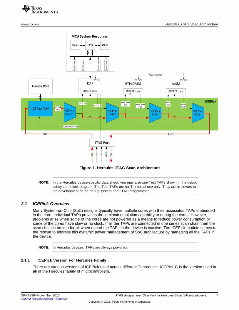
2 Hercules JTAG Scan ArchitectureFigure 1 shows an example superset implementation of the Hercules JTAG scan architecture. Somevariants of the Hercules family may not have the RTP/DMM TAPs implemented. For more information,check the device-specific data sheet. The TAP that is closest to the JTAG port is the ICEPick TAPcontroller. The ICEPick is TI's name for the JTAG route controller. Note that in the Hercules family, a fixedmapping is maintained across all devices. This means that the AJSM TAP will remain as the SDTAP2(Secondary Debug TAP 2) even if RTP/DMM TAP is not present in the device. ICEPick route controlleroffers the below features:• Dynamic scan chain management within the device• Interface multiple cores with different frequencies• It serves as a chip-level TAP controller for chip-level boundary scan and testing• Enabling emulation for security purposes on production devices
After reset, the ICEPick TAP is the only TAP connected in the JTAG scan chain as shown in Figure 1 withthe scan path highlighted in red. All other TAPs are classified as the secondary Debug TAPs. From theperspective of the external JTAG interface, secondary debug TAPs appear to not exist after reset.
2 JTAG Programmer Overview for Hercules-Based Microcontrollers SPNA230–November 2015Submit Documentation Feedback
Copyright © 2015, Texas Instruments Incorporated
ICEPick TAP
SDTAP0 Logic
DAP
JTAG Port
Device BSR
TDI
MCU TDIMCU TDO
ICEPick
TDO
SDTAP1 Logic
RTP/DMM
RTP/DMM
TDI RTP/DMM
TDO
SDTAP2 Logic
AJSM
AJSM
TDI AJSM
TDO
TDO
CPUFlash RAM
MCU System Resources
Pe
rip
he
ral
Pe
rip
he
ral
Pe
rip
he
ral
Pe
rip
he
ral
TD
I
TC
LK
TM
S
nT
RS
T
TD
O
TCLK/TMS/nTRST
ICEPick
ICEPick Switch
ICEPick Switch
ICEPick Switch
ICEPick Switch
AJSM_UNLOCK
TAP ena TAP ena TAP ena
1
www.ti.com Hercules JTAG Scan Architecture
Figure 1. Hercules JTAG Scan Architecture
NOTE: In the Hercules device-specific data sheet, you may also see Test TAPs shown in the debugsubsystem block diagram. The Test TAPs are for TI internal use only. They are irrelevant tothe development of the debug system and JTAG programmer.
2.1 ICEPick OverviewMany System-on-Chip (SoC) designs typically have multiple cores with their associated TAPs embeddedin the core. Individual TAPs provides the in-circuit emulation capability to debug the cores. However,problems arise when some of the cores are not powered as a means to reduce power consumption orsome of the cores have slow or no clock. If all the TAPs are connected in one series scan chain then thescan chain is broken for all when one of the TAPs in the device is inactive. The ICEPick module comes tothe rescue to address this dynamic power management of SoC architecture by managing all the TAPs inthe device.
NOTE: In Hercules devices, TAPs are always powered.
2.1.1 ICEPick Version For Hercules FamilyThere are various versions of ICEPIck used across different TI products. ICEPick-C is the version used inall of the Hercules family of microcontrollers.
3SPNA230–November 2015 JTAG Programmer Overview for Hercules-Based MicrocontrollersSubmit Documentation Feedback
Copyright © 2015, Texas Instruments Incorporated
Hercules JTAG Scan Architecture www.ti.com
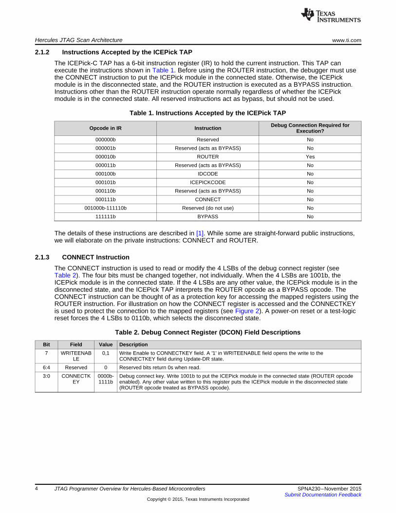
2.1.2 Instructions Accepted by the ICEPick TAPThe ICEPick-C TAP has a 6-bit instruction register (IR) to hold the current instruction. This TAP canexecute the instructions shown in Table 1. Before using the ROUTER instruction, the debugger must usethe CONNECT instruction to put the ICEPick module in the connected state. Otherwise, the ICEPickmodule is in the disconnected state, and the ROUTER instruction is executed as a BYPASS instruction.Instructions other than the ROUTER instruction operate normally regardless of whether the ICEPickmodule is in the connected state. All reserved instructions act as bypass, but should not be used.
Table 1. Instructions Accepted by the ICEPick TAP
Debug Connection Required forOpcode in IR Instruction Execution?000000b Reserved No000001b Reserved (acts as BYPASS) No000010b ROUTER Yes000011b Reserved (acts as BYPASS) No000100b IDCODE No000101b ICEPICKCODE No000110b Reserved (acts as BYPASS) No000111b CONNECT No
001000b-111110b Reserved (do not use) No111111b BYPASS No
The details of these instructions are described in [1]. While some are straight-forward public instructions,we will elaborate on the private instructions: CONNECT and ROUTER.
2.1.3 CONNECT InstructionThe CONNECT instruction is used to read or modify the 4 LSBs of the debug connect register (seeTable 2). The four bits must be changed together, not individually. When the 4 LSBs are 1001b, theICEPick module is in the connected state. If the 4 LSBs are any other value, the ICEPick module is in thedisconnected state, and the ICEPick TAP interprets the ROUTER opcode as a BYPASS opcode. TheCONNECT instruction can be thought of as a protection key for accessing the mapped registers using theROUTER instruction. For illustration on how the CONNECT register is accessed and the CONNECTKEYis used to protect the connection to the mapped registers (see Figure 2). A power-on reset or a test-logicreset forces the 4 LSBs to 0110b, which selects the disconnected state.
Table 2. Debug Connect Register (DCON) Field Descriptions
Bit Field Value Description7 WRITEENAB 0,1 Write Enable to CONNECTKEY field. A '1' in WRITEENABLE field opens the write to the
LE CONNECTKEY field during Update-DR state.6:4 Reserved 0 Reserved bits return 0s when read.3:0 CONNECTK 0000b- Debug connect key. Write 1001b to put the ICEPick module in the connected state (ROUTER opcode
EY 1111b enabled). Any other value written to this register puts the ICEPick module in the disconnected state(ROUTER opcode treated as BYPASS opcode).
4 JTAG Programmer Overview for Hercules-Based Microcontrollers SPNA230–November 2015Submit Documentation Feedback
Copyright © 2015, Texas Instruments Incorporated
32-bit Data Shift Register
32-bit IDCODE
Reg
32-bit ICEPICK
CODE Reg
8-bit Debug
CONNECT Reg
Key
Decode
Read the selected Reg
During Capture-DR state
Write the selected Reg
During Update-DR state
32 bits
24-bit
SYS_CNTL Reg
24-bit SDTAP0
Reg for DAP
24-bit SDTAP1
Reg DMMRTP
24-bit SDTAP2
Reg for AJSM
ROUTER
Decode
IR
Decode
6-bit IR Register
TDOTDI
Bits[7:0]
connect
Bits[23:0] = DATA
Bit[31] = R/W
Bit[30:24] = REG
www.ti.com Hercules JTAG Scan Architecture
Figure 2. Conceptual ICEPICK-C Block Diagram for Hercules Implementation
2.1.3.1 Reading the Debug Connect RegisterTo read the debug connect register:1. Move the ICEPick TAP to the Shift-IR state, shift in the 6-bit CONNECT instruction (000111b) to the IR
register for six cycles2. Move to the Update-IR state, the CONNECT instruction becomes the current instruction3. Move the ICEPick TAP to the Shift-DR state, while in Shift-DR state shift in the 8 bits of register-
access information LSB first. Since the operation is to perform a read, bit 7 must be 0 and the rest ofbits are don't care.
4. Once the TAP advances to the Update-DR state, the content of the Data Shift Register value isupdated (written in parallel) to the DCON register. Since bit 7 indicating a read is written to the DCONregister, bits[6:0] of the DCON register aren't affected in Update-DR state.
5SPNA230–November 2015 JTAG Programmer Overview for Hercules-Based MicrocontrollersSubmit Documentation Feedback
Copyright © 2015, Texas Instruments Incorporated
Hercules JTAG Scan Architecture www.ti.com
5. Move the TAP to the Capture-DR state, the content of the DCON register is captured to the data shiftregister.
6. Move the TAP to the Shift-DR state, the content of the shift register which contains the value of theDCON register is shifted out.
2.1.3.2 Writing the Debug Connect RegisterTo write the debug connect register:1. Move the ICEPick TAP to the Shift-IR state, shift in the 6-bit CONNECT instruction (000111b) to the IR
register for six cycles2. Move to the Update-IR state, the CONNECT instruction becomes the current instruction3. Move the ICEPick TAP to the Shift-DR state, while in Shift-DR state shift in the 8 bits of register-
access information LSB first. Since the operation is to perform a write to the CONNECTKEY field, bit 7must be 1. In order to open access to the mapped registers, a value of 1001b should be scanned intobits[3:0] of the DCON register. Bits[6:4] are don't care.
4. Once the TAP advances to the Update-DR state, the Data Shift Register value is updated (written inparallel) to the DCON register. If the ICEPick module is in the disconnected state, the ROUTERopcode is interpreted as a BYPASS opcode.
2.1.4 ROUTER InstructionThere are four 24-bit mapped registers in ICEPICK-C implemented for the Hercules devices (see Figure 2and Table 3). These registers can only be accessed when the ROUTER instruction (000010b) is thecurrent IR instruction. To access the ROUTER instruction, the ICEPick module must first be in the connectstate by following the instructions in Section 2.1.3.2.
For the ROUTER instruction, all 32 bits of the ICEPick data shift register are placed between TDI andTDO in the SELECT DR state. In the SHIFT DR state, the 32 bits shifted in must have the format shown inFigure 3. When a value is scanned in, bit 31 indicates whether the register is to be read or written, bits30–24 indicate which register is to be accessed, and bits 23–0 contain the data (if any). When a value isscanned out, bit 31 indicates whether the previous write succeeded (0) or failed (1), bits 30–24 indicatewhich register was read, and bits 23–0 contain the data.
Figure 3. Fields of the 32-Bit Scan Value for Accessing Mapped Registers31 30 24 23 16
R_W/F REG DATA[23:16]AIL
15 0DATA[15:0]
Table 3. Mapped Register Selection
REG Register000_0000b All zeros000_0001b System control register (SYS_CNTL)010_0000b Secondary Debug TAP 0 register (SDTAP0) for DAP010_0001b Secondary Debug TAP 1 register (SDTAP1) for RTP/DMM010_0010b Secondary Debug TAP 2 register (SDTAP2) for AJSM
2.1.4.1 Reading a Mapped RegisterTo read a mapped register through the ICEPick TAP:1. Make sure that CONNECT instruction has been issued to put the ICEPick in a connect state as
depicted in Section 2.1.3.2.2. Move the ICEPick TAP to Shift-IR state, shift in the ROUTER instruction (000010b) for six cycles.
6 JTAG Programmer Overview for Hercules-Based Microcontrollers SPNA230–November 2015Submit Documentation Feedback
Copyright © 2015, Texas Instruments Incorporated
www.ti.com Hercules JTAG Scan Architecture
3. Move to the Update-IR state, the ROUTER instruction becomes the current instruction.4. Move the ICEPick TAP to the Shift-DR state, while in the Shift-DR state, shift in the 32 bits of register-
access information. Bit 31 must be 0 for a read. For example, to read the SDTAP0 Reg for DAP, thevalue to be scanned in would be 0x20xxxxxx
5. Move the ICEPick TAP to the Update-DR state, and the mapped register to be selected for accessed isdecoded according to the value of REG (bits[30-24] of the Data Shift register). and bits 23–0 are don'tcare bits.
6. Move the TAP to the Capture-DR state, the content of the selected register (SDTAP0 Reg) is updated(written in parallel) to the Data Shift register.
7. Move the TAP to the Shift-DR state, the content of the shift register which contains the value of theselected mapped register (SDTAP0 Reg) is shifted out. While the value is being shifted out, newregister-access information (for a read or a write) can be shifted in.
8. Perform another DR scan to capture and shift out the content of the register.
Multiple registers can be read in sequence without the need to scan in another ROUTER instruction.
2.1.4.2 Writing to a Mapped RegisterTo load a mapped register through the ICEPick TAP:1. Make sure that CONNECT instruction has been issued to put the ICEPick in a connect state as
depicted in Section 2.1.3.2.2. Move the ICEPick TAP to Shift-IR state, shift in the ROUTER instruction (000010b) for six cycles.3. Move to the Update-IR state, the ROUTER instruction becomes the current instruction.4. Move the ICEPick TAP to the Shift-DR state, while in the Shift-DR state, shift in the 32 bits of register-
access information. Bit 31 must be 1 for a write. For example, to write the SYS_CNTL Reg, the valueto be scanned in would be 0x81xxxxxx where xxxxxx is the value to be written to SYS_CNTL register.
5. When the TAP advances to the UPDATE DR state, the register-access information according to theREG field in bits[30:24] is decoded and the data is written to the register.
Multiple registers can be loaded in sequence without the need to scan in another ROUTER instruction. Inthis case, after each value is written, the output of the subsequent scan shows the value written.
2.1.5 ICEPick Mapped RegistersTable 3 lists the four ICEPick mapped registers implemented for Hercules family. The details of theseregisters are described in [1].
2.1.5.1 System Control Register (SYS_CNTL)Not all features of SYS_CNTL register are applicable to the Hercules family. This section clarifies whichfeatures are applicable.• Feature: Adaptative Clock Control
– Feature description: The benefit of adaptive clocking is to ensure that TCK is running at the highestpossible frequency no matter what the ARM core clock is. The scheme automatically scales TCKas the ARM clock scales. Adaptative clocking is achieved by using both the TCK and RTCK. Whenadaptive clocking is selected the emulator sends a TCK signal and waits for the Return TCK(RTCK) to come back. The emulator does not progress to the next TCK until RTCK is received.
– Feature applicability: Hercules family uses the Cortex-R cores which do not have RTCK, so are notaffected.
• Feature: ICEPick Power Management– Feature description: Keep the ICEPick logic powered even when the ICEPick TAP enters the TEST
LOGIC RESET state.– Feature applicability: This feature has no effect on Hercules family. The ICEPick is always powered
• Feature: TDO Control– Feature description: Force the TDO pin to be in the output state regardless of the TAP state
7SPNA230–November 2015 JTAG Programmer Overview for Hercules-Based MicrocontrollersSubmit Documentation Feedback
Copyright © 2015, Texas Instruments Incorporated
Hercules JTAG Scan Architecture www.ti.com
– Feature applicability: This feature is applicable to Hercules family• Feature: Device Type
– Feature description: Read the factory-programmable device type.– Feature applicability: This feature is applicable to Hercules family
• Feature: Initiate a System Reset– Feature description: A system reset acts as a warm reset to the entire device. Majority of the device
is reset by warm reset in Hercules family except the debug logic and some logic which are onlyreset by the cold reset, the nPORRST. An ICEPick reset is equivalent in effect to issuing a nRST.
– Feature applicability: This feature is applicable to Hercules family
2.1.5.2 SDTAPx RegisterEach secondary debug TAP register (SDTAPx) includes fields for controlling and monitoring power andclock states of the secondary TAP and its associated module. Features related to power control are notapplicable to Hercules family.• Features: Power Management
– Feature descriptions: Bit fields POWERLOSSDETECTED, INHIBITSLEEP, TAPPOWER,FORCEPOWER, POWER, CLOCKDOWNDESIRED are various controls to manage the power andclock of the respective TAP and its associated module.
– Feature applicability: These features are not applicable to Hercules family• Features: Reset Control and Status
– Feature descriptions: Bits fields UNNATURALRESET, RELEASEFROMWIR, RESETCONTROL arecontrol and status for debugger reset management.
– Feature applicability: Applicable to Hercules family.• Features: Debug Control and Status
– Feature descriptions: Bits fields DEBUGCONNECT, DEBUGMODE, DEBUGATTENTION are usedto enable and configure debug mode of the respective debug component.
– Feature applicability: Applicable to Hercules family.• Features: TAP Control and Status
– Feature descriptions: Bits fields TAPVISIBLE, TAPSELECT, TAPACCESSABLE and TAPRESENTare used to select the respective TAP in the JTAG scan chain and indicate the status of theconnected TAP.
– Feature applicability: Applicable to Hercules family.
2.1.5.3 Selecting DAP TAPAs mentioned in the beginning, the ICEPick TAP is the only TAP in the JTAG scan chain after reset. Toselect other TAP such as the TAP for the Debug Access Port (DAP) the tools must write to the SDTAP0register. In addition, the device must not be in a secured state (see Section 2.2). Details of selecting DAPTAP can be found in [4]. Follow the steps below:1. Move the ICEPick TAP to the Shift-IR state, shift in the 6-bit CONNECT instruction (000111b) to the IR
register for six cycles2. Move to the Update-IR state, the CONNECT instruction becomes the current instruction3. Move the ICEPick TAP to the Shift-DR state, while in Shift-DR state shift in the 8-bit value 10001001b
with LSB first.4. Move the ICEPick TAP to the Update-DR state, this operation will put the ICEPick in connect state.5. Move the ICEPick TAP to the Shift-IR state again, shift in the 6-bit ROUTER instruction (000010b) to
the IR register for six cycles6. Move to the Update-IR state, the ROUTER instruction becomes the current instruction7. Move the ICEPick TAP to the Shift-DR state, while in Shift-DR state shift in the 32-bit value a0002108h
with LSB first.• bit[31] = 1 indicates a write operation
8 JTAG Programmer Overview for Hercules-Based Microcontrollers SPNA230–November 2015Submit Documentation Feedback
Copyright © 2015, Texas Instruments Incorporated
ICEPick TAP
SDTAP0 Logic
DAP
JTAG Port
Device BSR
TDI
MCU TDIMCU TDO
ICEPick
TDO
SDTAP1 Logic
RTP/DMM
RTP/DMM
TDI RTP/DMM
TDO
SDTAP2 Logic
AJSM
AJSM
TDI AJSM
TDO
TDO
CPUFlash RAM
MCU System Resources
Pe
rip
he
ral
Pe
rip
he
ral
Pe
rip
he
ral
Pe
rip
he
ral
TD
I
TC
LK
TM
S
nT
RS
T
TD
O
TCLK/TMS/nTRST
ICEPick
ICEPick Switch
ICEPick Switch
ICEPick Switch
ICEPick Switch
AJSM_UNLOCK
TAP ena TAP ena TAP ena
1
www.ti.com Hercules JTAG Scan Architecture
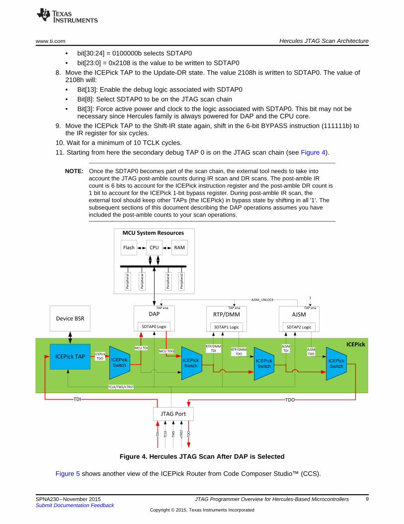
• bit[30:24] = 0100000b selects SDTAP0• bit[23:0] = 0x2108 is the value to be written to SDTAP0
8. Move the ICEPick TAP to the Update-DR state. The value 2108h is written to SDTAP0. The value of2108h will:• Bit[13]: Enable the debug logic associated with SDTAP0• Bit[8]: Select SDTAP0 to be on the JTAG scan chain• Bit[3]: Force active power and clock to the logic associated with SDTAP0. This bit may not be
necessary since Hercules family is always powered for DAP and the CPU core.9. Move the ICEPick TAP to the Shift-IR state again, shift in the 6-bit BYPASS instruction (111111b) to
the IR register for six cycles.10. Wait for a minimum of 10 TCLK cycles.11. Starting from here the secondary debug TAP 0 is on the JTAG scan chain (see Figure 4).
NOTE: Once the SDTAP0 becomes part of the scan chain, the external tool needs to take intoaccount the JTAG post-amble counts during IR scan and DR scans. The post-amble IRcount is 6 bits to account for the ICEPick instruction register and the post-amble DR count is1 bit to account for the ICEPick 1-bit bypass register. During post-amble IR scan, theexternal tool should keep other TAPs (the ICEPick) in bypass state by shifting in all '1'. Thesubsequent sections of this document describing the DAP operations assumes you haveincluded the post-amble counts to your scan operations.
Figure 4. Hercules JTAG Scan After DAP is Selected
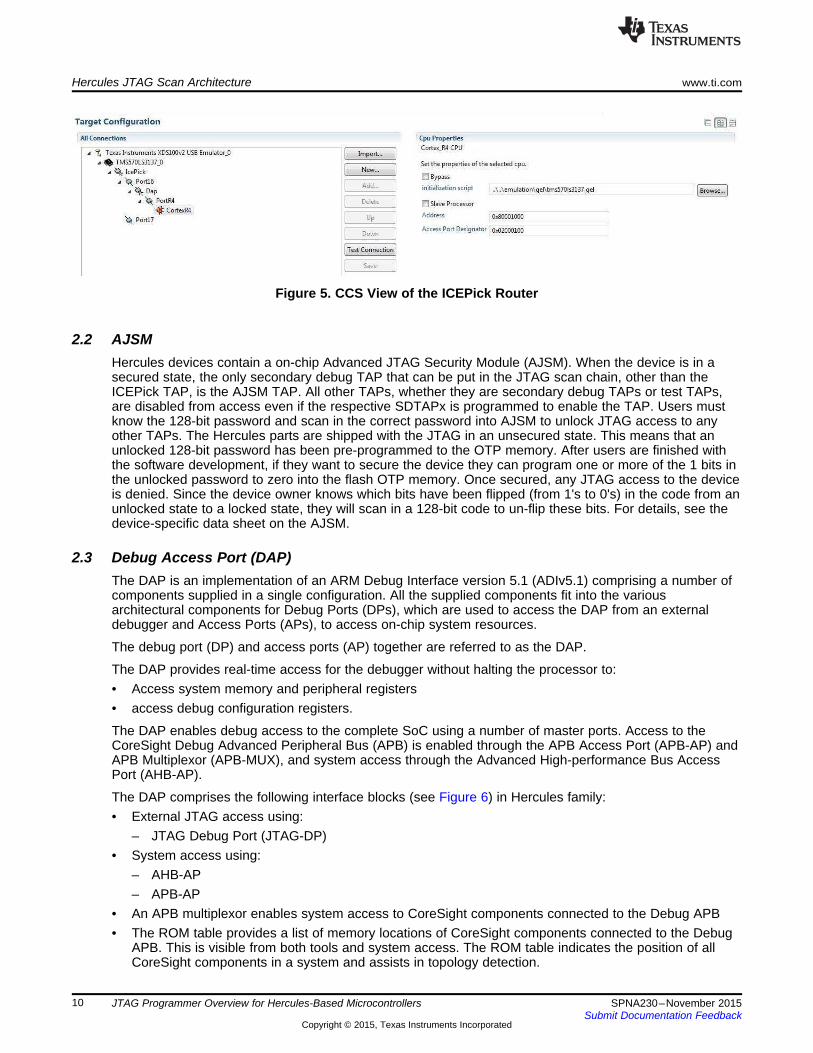
Figure 5 shows another view of the ICEPick Router from Code Composer Studio™ (CCS).
9SPNA230–November 2015 JTAG Programmer Overview for Hercules-Based MicrocontrollersSubmit Documentation Feedback
Copyright © 2015, Texas Instruments Incorporated
Hercules JTAG Scan Architecture www.ti.com
Figure 5. CCS View of the ICEPick Router
2.2 AJSMHercules devices contain a on-chip Advanced JTAG Security Module (AJSM). When the device is in asecured state, the only secondary debug TAP that can be put in the JTAG scan chain, other than theICEPick TAP, is the AJSM TAP. All other TAPs, whether they are secondary debug TAPs or test TAPs,are disabled from access even if the respective SDTAPx is programmed to enable the TAP. Users mustknow the 128-bit password and scan in the correct password into AJSM to unlock JTAG access to anyother TAPs. The Hercules parts are shipped with the JTAG in an unsecured state. This means that anunlocked 128-bit password has been pre-programmed to the OTP memory. After users are finished withthe software development, if they want to secure the device they can program one or more of the 1 bits inthe unlocked password to zero into the flash OTP memory. Once secured, any JTAG access to the deviceis denied. Since the device owner knows which bits have been flipped (from 1's to 0's) in the code from anunlocked state to a locked state, they will scan in a 128-bit code to un-flip these bits. For details, see thedevice-specific data sheet on the AJSM.
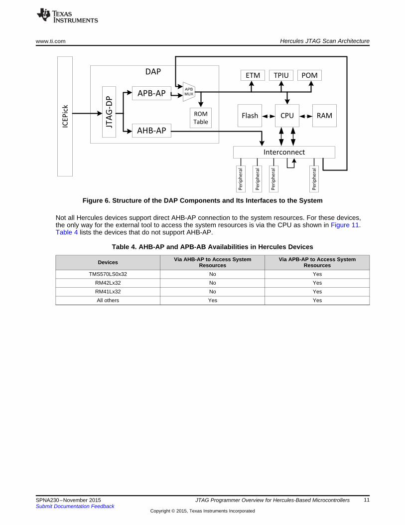
2.3 Debug Access Port (DAP)The DAP is an implementation of an ARM Debug Interface version 5.1 (ADIv5.1) comprising a number ofcomponents supplied in a single configuration. All the supplied components fit into the variousarchitectural components for Debug Ports (DPs), which are used to access the DAP from an externaldebugger and Access Ports (APs), to access on-chip system resources.
The debug port (DP) and access ports (AP) together are referred to as the DAP.
The DAP provides real-time access for the debugger without halting the processor to:• Access system memory and peripheral registers• access debug configuration registers.
The DAP enables debug access to the complete SoC using a number of master ports. Access to theCoreSight Debug Advanced Peripheral Bus (APB) is enabled through the APB Access Port (APB-AP) andAPB Multiplexor (APB-MUX), and system access through the Advanced High-performance Bus AccessPort (AHB-AP).
The DAP comprises the following interface blocks (see Figure 6) in Hercules family:• External JTAG access using:
– JTAG Debug Port (JTAG-DP)• System access using:
– AHB-AP– APB-AP
• An APB multiplexor enables system access to CoreSight components connected to the Debug APB• The ROM table provides a list of memory locations of CoreSight components connected to the Debug
APB. This is visible from both tools and system access. The ROM table indicates the position of allCoreSight components in a system and assists in topology detection.
10 JTAG Programmer Overview for Hercules-Based Microcontrollers SPNA230–November 2015Submit Documentation Feedback
Copyright © 2015, Texas Instruments Incorporated
JTAG-DP
DAP
CPUFlash RAM
AHB-AP
APB-APAPBMUX
ROM
Table
ICEPick
ETM TPIU POM
Peripheral
Peripheral
Peripheral
Peripheral
Interconnect
www.ti.com Hercules JTAG Scan Architecture
Figure 6. Structure of the DAP Components and Its Interfaces to the System
Not all Hercules devices support direct AHB-AP connection to the system resources. For these devices,the only way for the external tool to access the system resources is via the CPU as shown in Figure 11.Table 4 lists the devices that do not support AHB-AP.
Table 4. AHB-AP and APB-AB Availabilities in Hercules Devices
Via AHB-AP to Access System Via APB-AP to Access SystemDevices Resources ResourcesTMS570LS0x32 No Yes
RM42Lx32 No YesRM41Lx32 No YesAll others Yes Yes
11SPNA230–November 2015 JTAG Programmer Overview for Hercules-Based MicrocontrollersSubmit Documentation Feedback
Copyright © 2015, Texas Instruments Incorporated
JTAG-DP
DAP
CPUFlash RAM
Peripheral
Peripheral
Peripheral
Peripheral
AHB-AP
APB-APAPBMUX
ROM
Table
ICEPick
Interconnect
ETM TPIU POM
JTAG-DP
DAP
CPUFlash RAM
Peripheral
Peripheral
Peripheral
Peripheral
AHB-AP
APB-APAPBMUX
ROM
Table
ICEPick
Interconnect
ETM TPIU POM
Hercules JTAG Scan Architecture www.ti.com
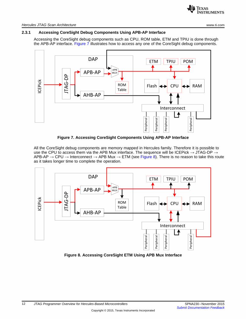
2.3.1 Accessing CoreSight Debug Components Using APB-AP InterfaceAccessing the CoreSight debug components such as CPU, ROM table, ETM and TPIU is done throughthe APB-AP interface. Figure 7 illustrates how to access any one of the CoreSight debug components.
Figure 7. Accessing CoreSight Components Using APB-AP Interface
All the CoreSight debug components are memory mapped in Hercules family. Therefore it is possible touse the CPU to access them via the APB Mux interface. The sequence will be ICEPick → JTAG-DP →APB-AP → CPU → Interconnect → APB Mux → ETM (see Figure 8). There is no reason to take this routeas it takes longer time to complete the operation.
Figure 8. Accessing CoreSight ETM Using APB Mux Interface
12 JTAG Programmer Overview for Hercules-Based Microcontrollers SPNA230–November 2015Submit Documentation Feedback
Copyright © 2015, Texas Instruments Incorporated
JTAG-DP
DAP
CPUFlash RAM
Peripheral
Peripheral
Peripheral
Peripheral
AHB-AP
APB-APAPBMUX
ROM
Table
ICEPick
Interconnect
ETM TPIU POM
JTAG-DP
DAP
CPUFlash RAM
Peripheral
Peripheral
Peripheral
Peripheral
AHB-AP
APB-APAPBMUX
ROM
Table
ICEPick
Interconnect
ETM TPIU POM
www.ti.com Hercules JTAG Scan Architecture
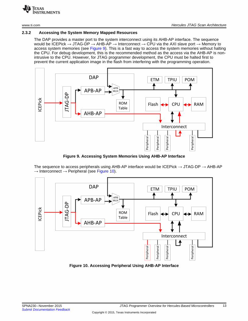
2.3.2 Accessing the System Memory Mapped ResourcesThe DAP provides a master port to the system interconnect using its AHB-AP interface. The sequencewould be ICEPick → JTAG-DP → AHB-AP → Interconnect → CPU via the AXI slave port → Memory toaccess system memories (see Figure 9). This is a fast way to access the system memories without haltingthe CPU. For debug development, this is the recommended method as the access via the AHB-AP is non-intrusive to the CPU. However, for JTAG programmer development, the CPU must be halted first toprevent the current application image in the flash from interfering with the programming operation.
Figure 9. Accessing System Memories Using AHB-AP Interface
The sequence to access peripherals using AHB-AP interface would be ICEPick → JTAG-DP → AHB-AP→ Interconnect → Peripheral (see Figure 10).
Figure 10. Accessing Peripheral Using AHB-AP Interface
13SPNA230–November 2015 JTAG Programmer Overview for Hercules-Based MicrocontrollersSubmit Documentation Feedback
Copyright © 2015, Texas Instruments Incorporated
JTAG-DP
DAP
CPUFlash RAM
Peripheral
Peripheral
Peripheral
Peripheral
AHB-AP
APB-APAPBMUX
ROM
Table
ICEPick
Interconnect
ETM TPIU POM
Hercules JTAG Scan Architecture www.ti.com
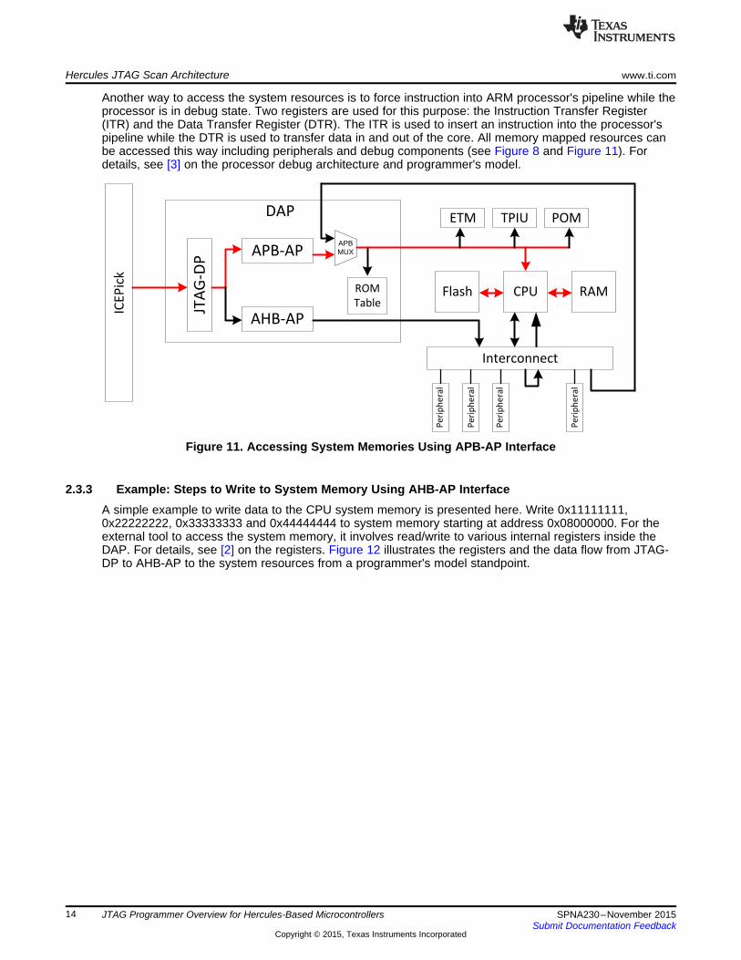
Another way to access the system resources is to force instruction into ARM processor's pipeline while theprocessor is in debug state. Two registers are used for this purpose: the Instruction Transfer Register(ITR) and the Data Transfer Register (DTR). The ITR is used to insert an instruction into the processor'spipeline while the DTR is used to transfer data in and out of the core. All memory mapped resources canbe accessed this way including peripherals and debug components (see Figure 8 and Figure 11). Fordetails, see [3] on the processor debug architecture and programmer's model.
Figure 11. Accessing System Memories Using APB-AP Interface
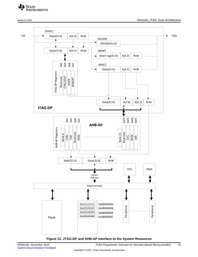
2.3.3 Example: Steps to Write to System Memory Using AHB-AP InterfaceA simple example to write data to the CPU system memory is presented here. Write 0x11111111,0x22222222, 0x33333333 and 0x44444444 to system memory starting at address 0x08000000. For theexternal tool to access the system memory, it involves read/write to various internal registers inside theDAP. For details, see [2] on the registers. Figure 12 illustrates the registers and the data flow from JTAG-DP to AHB-AP to the system resources from a programmer's model standpoint.
14 JTAG Programmer Overview for Hercules-Based Microcontrollers SPNA230–November 2015Submit Documentation Feedback
Copyright © 2015, Texas Instruments Incorporated
Data[31:0] A[3:2] RnW
Re
serv
ed
CT
RL/
ST
AT
AD
DR
RD
BU
FF
0x0
0x4
0x8
0xC
JTA
G-D
P R
eg
iste
rs
Data[31:0] A[3:2] RnW
IDCODE[31:0]
Abort reg[31:0] A[3:2] RnW
Data[31:0] A[3:2] RnW
DPACC
IDCODE
ABORT
APACC
TDI TDO
Data[31:0] A[3:2] RnWA[7:4]
CS
W
TA
R
Re
serv
ed
DR
W
0x0
0x4
0x8
0xC
AH
B-A
P R
eg
iste
rs
Ba
nk
0
Re
serv
ed
CF
G
BA
SE
IDR
0xF
0
0xF
4
0xF
8
0xF
C
Ba
nk
15
Data[31:0] RnWAddr[31:0]
Interconnect
CPU DMA
System
AHB Bus
Pe
rip
he
ral
Pe
rip
he
ral0x11111111
0x22222222
0x33333333
0x44444444
0x08000000
0x08000004
0x08000008
0x0800000CFlash
JTAG-DP
AHB-AP
www.ti.com Hercules JTAG Scan Architecture
Figure 12. JTAG-DP and AHB-AP Interface to the System Resources
15SPNA230–November 2015 JTAG Programmer Overview for Hercules-Based MicrocontrollersSubmit Documentation Feedback
Copyright © 2015, Texas Instruments Incorporated
Hercules JTAG Scan Architecture www.ti.com
NOTE: Before you start sending commands to the DAP, make sure the ICEPick is properly setupand the DAP is selected in the scan chain according to the instructions outlined inSection 2.1.5.3.
Power-up handshake (optional for Hercules family):• Write 0x50000000 to the JTAG-DP.CTRL/STAT register. The value 0x50000000 sets bit[30] and bit[28]
of the register to generate power up request to the power controller. The step to request power isoptional in Hercules family as Hercules DAP is in always-ON power domain.1. Move TAP to shift-IR to scan in the 4-bit DPACC instruction (1010b). In Update-IR, DPACC
becomes the current instruction.2. Move TAP to Shift-DR to scan in a value of 50000000 & 01b & 0b. Of the 35-bit value to be
scanned in, the upper 32 bits represents the data to be written to the DPACC offset address 01b atwhich the CTRL/STAT register resides. Bit[0]=0 indicates this is a write operation.
3. Move TAP to Update-DR, the write happens to the CTRL/STAT register.• Poll the JTAG-DP.CTRL/STAT register for 0xf0000000. Bit[31:28] should be 1111b to indicate power
request is acknowledged by the power controller. This step is optional in Hercules family as HerculesDAP is in always powered.1. Move TAP to Shift-DR to scan in a value of xxxxxxxxh & 01b & 1b. This is to perform a read of the
CTRL/STAT register.2. Move TAP to Capture-DR state to capture the power up acknowledgment status from CTRL/STAT
register.3. Move TAP to Shift-DR state to scan out the status. The external tool should repeat these three
steps until the power is ready before moving to the next step.
Activate AHB-AP:• Write 0x0 to the JTAG-DP.ADDR register to activate AHB-AP. Bit[31:24]=0x0 selects the AHB-AP.
Bit[7:4]=0x0 selects the bank 0 within AHB-AP. In the subsequent operation we will perform writes toregisters residing in bank 0 of the AHB-AP module.1. Move TAP to Shift-DR to scan in a value of 0x0 & 10b & 0b. Of the 35-bit value to be scanned in,
the upper 32 bits represents the data to be written to the DPACC offset address 10b at which theADDR register resides. Bit[0]=0 indicates this is a write operation.
2. Move TAP to Update-DR, the write happens to the ADDR register. The AHB-AP is selected afterthe write.
Set the AHB-AP access protection mode and address mode:• Write 0x43000012 to the AHB-AP.CSW register. The value written is to encode the AHB-AP bus
transactions to the system memory in non-secure, non-exclusive, non-cacheable, non-bufferable, dataaccess and privileged mode with 32-bit transaction size. It also enables address increment mode.1. Move TAP to shift-IR to scan in the 4-bit APACC instruction (1011b). In Update-IR, APACC
becomes the current instruction.2. Move TAP to Shift-DR to scan in a value of 0x43000012 & 00b & 0b. Of the 35-bit value to be
scanned in, the upper 32 bits represents the data to be written to the AHB-AP offset address 00b atwhich the Control/Status Word, CSW register resides. Bit[0]=0 indicates this is a write operation.
NOTE: While new data is shifted in, the read data of the previous transaction (the writetransaction to ADDR register) and the nCONT flag is shifted out. nCONT is a ready flagmechanism to determine if the current transaction can complete. External tool shouldevaluate the nCONT to take necessary action, i.e. to early terminate the currenttransaction and repeat.
3. Move TAP to Update-DR, the write happens to the CSW register.
Set the AHB-AP address to access:• Write 0x08000000 to the AHB-AP.TAR register.
16 JTAG Programmer Overview for Hercules-Based Microcontrollers SPNA230–November 2015Submit Documentation Feedback
Copyright © 2015, Texas Instruments Incorporated
www.ti.com Hercules JTAG Scan Architecture
1. Move TAP to Shift-DR to scan in a value of 0x08000000 & 01b & 0b. Of the 35-bit value to bescanned in, the upper 32 bits represents the address to be written to the AHB-AP offset address01b at which the TAR (Transfer Address) register resides. Bit[0]=0 indicates this is a writeoperation.
2. Move TAP to Update-DR, the write happens to the TAR register.
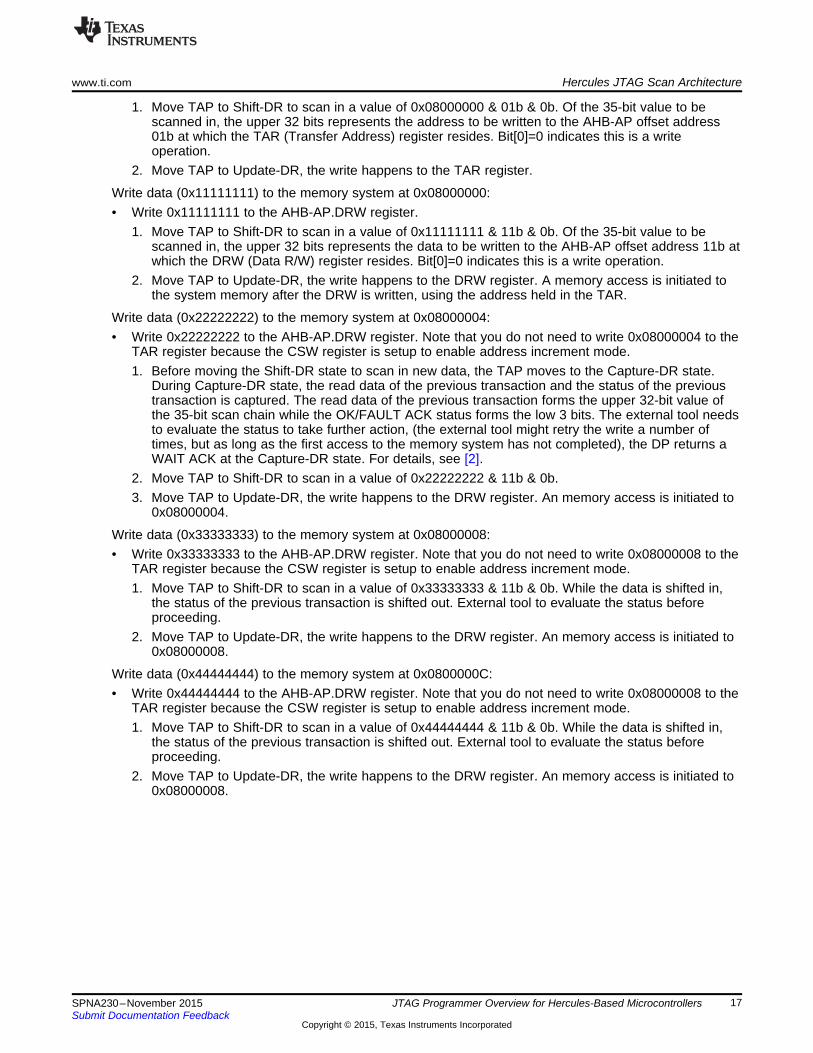
Write data (0x11111111) to the memory system at 0x08000000:• Write 0x11111111 to the AHB-AP.DRW register.
1. Move TAP to Shift-DR to scan in a value of 0x11111111 & 11b & 0b. Of the 35-bit value to bescanned in, the upper 32 bits represents the data to be written to the AHB-AP offset address 11b atwhich the DRW (Data R/W) register resides. Bit[0]=0 indicates this is a write operation.
2. Move TAP to Update-DR, the write happens to the DRW register. A memory access is initiated tothe system memory after the DRW is written, using the address held in the TAR.
Write data (0x22222222) to the memory system at 0x08000004:• Write 0x22222222 to the AHB-AP.DRW register. Note that you do not need to write 0x08000004 to the
TAR register because the CSW register is setup to enable address increment mode.1. Before moving the Shift-DR state to scan in new data, the TAP moves to the Capture-DR state.
During Capture-DR state, the read data of the previous transaction and the status of the previoustransaction is captured. The read data of the previous transaction forms the upper 32-bit value ofthe 35-bit scan chain while the OK/FAULT ACK status forms the low 3 bits. The external tool needsto evaluate the status to take further action, (the external tool might retry the write a number oftimes, but as long as the first access to the memory system has not completed), the DP returns aWAIT ACK at the Capture-DR state. For details, see [2].
2. Move TAP to Shift-DR to scan in a value of 0x22222222 & 11b & 0b.3. Move TAP to Update-DR, the write happens to the DRW register. An memory access is initiated to
0x08000004.
Write data (0x33333333) to the memory system at 0x08000008:• Write 0x33333333 to the AHB-AP.DRW register. Note that you do not need to write 0x08000008 to the
TAR register because the CSW register is setup to enable address increment mode.1. Move TAP to Shift-DR to scan in a value of 0x33333333 & 11b & 0b. While the data is shifted in,
the status of the previous transaction is shifted out. External tool to evaluate the status beforeproceeding.
2. Move TAP to Update-DR, the write happens to the DRW register. An memory access is initiated to0x08000008.
Write data (0x44444444) to the memory system at 0x0800000C:• Write 0x44444444 to the AHB-AP.DRW register. Note that you do not need to write 0x08000008 to the
TAR register because the CSW register is setup to enable address increment mode.1. Move TAP to Shift-DR to scan in a value of 0x44444444 & 11b & 0b. While the data is shifted in,
the status of the previous transaction is shifted out. External tool to evaluate the status beforeproceeding.
2. Move TAP to Update-DR, the write happens to the DRW register. An memory access is initiated to0x08000008.
17SPNA230–November 2015 JTAG Programmer Overview for Hercules-Based MicrocontrollersSubmit Documentation Feedback
Copyright © 2015, Texas Instruments Incorporated
Hercules JTAG Scan Architecture www.ti.com
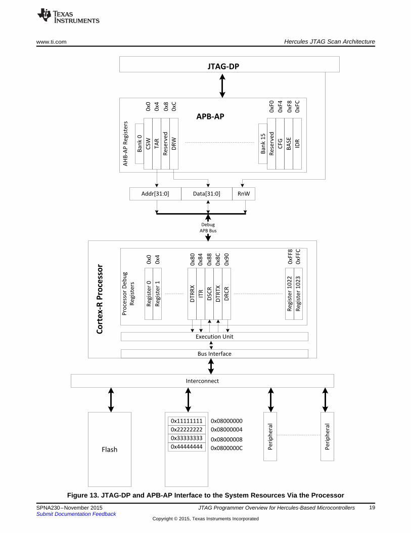
2.3.4 Example: Steps to Write to System Memory Using APB-AP InterfaceA simple example is presented to write data to the CPU system memory using the CPU in debug state.Write 0x11111111 to system memory starting at address 0x08000000. Figure 13 illustrates the registersand the data flow from JTAG-DP to APB-AP to CPU's debug component from a programmer's modelstandpoint. For simplicity reason, all system resources (Flash, SRAM, peripherals) are connected to theCPU via an interconnect. The graphic does not represent the actual implementation of the busarchitecture in the Hercules devices. For details, see the device-specific data sheet and TRM. Thedrawing illustrates the system resources with respect to the CPU and the DAP from a programmer's modelstandpoint.
18 JTAG Programmer Overview for Hercules-Based Microcontrollers SPNA230–November 2015Submit Documentation Feedback
Copyright © 2015, Texas Instruments Incorporated
CS
W
TA
R
Re
serv
ed
DR
W
0x0
0x4
0x8
0xC
AH
B-A
P R
eg
iste
rs
Ba
nk
0
Re
serv
ed
CF
G
BA
SE
IDR
0xF
0
0xF
4
0xF
8
0xF
C
Ba
nk
15
Data[31:0] RnWAddr[31:0]
Interconnect
Debug
APB Bus
Pe
rip
he
ral
Pe
rip
he
ral0x11111111
0x22222222
0x33333333
0x44444444
0x08000000
0x08000004
0x08000008
0x0800000CFlash
APB-AP
JTAG-DP
Re
gis
ter
0
Re
gis
ter
1
DT
RR
X
ITR
0x0
0x4
0x8
0
0x8
4
Pro
cess
or
De
bu
g
Re
gis
ters
DS
CR
DT
RT
X
Re
gis
ter
10
22
Re
gis
ter
10
23
0x8
8
0x8
C
0xF
F8
0xF
FC
Co
rte
x-R
Pro
ce
sso
r
DR
CR
0x9
0
Bus Interface
Execution Unit
www.ti.com Hercules JTAG Scan Architecture
Figure 13. JTAG-DP and APB-AP Interface to the System Resources Via the Processor
19SPNA230–November 2015 JTAG Programmer Overview for Hercules-Based MicrocontrollersSubmit Documentation Feedback
Copyright © 2015, Texas Instruments Incorporated
Hercules JTAG Scan Architecture www.ti.com
To use the CPU to read and write data to the system resources requires the external tool to force ARMinstructions into the processor's pipeline. Since the example is to write data of 0x11111111 to the address0x08000000, it can be represented by the below ARM instructions.STR R0, [R1] ; R0=0x11111111
; R1=0x08000000
There are three high-level steps involved:• Load the R0 register with 0x11111111• Load the R1 register with 0x08000000• Execute STR R0, [R1] instruction
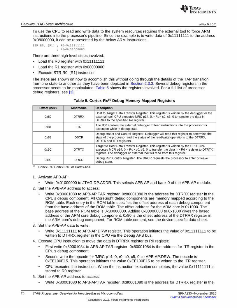
The steps are shown on how to accomplish this without going through the details of the TAP transitionfrom one state to another as they have been depicted in Section 2.3.3. Several debug registers in theprocessor needs to be manipulated. Table 5 shows the registers involved. For a full list of processordebug registers, see [3].
Table 5. Cortex-Rx (1) Debug Memory-Mapped Registers
Offset (hex) Mnemonic DescriptionHost to Target Data Transfer Register. This register is written by the debugger or the
0x80 DTRRX external tool. CPU executes MRC p14, 0, <Rd> c0, c5, 0 to transfer the data inDTRRX to the specified Rd register.The ITR enables the external debugger to feed instructions into the processor for0x84 ITR execution while in debug state.Debug status and Control Register. Debugger will read this register to determine the
0x88 DSCR state of the processor and the status of the read/write operations to the DTRRX,DTRTX and ITR registers.Target to Host Data Transfer Register. This register is written by the CPU. CPU
0x8C DTRTX executes MCR p14, 0, <Rd> c0, c5, 0 to transfer the data in <Rd> register to DTRTXregister. The debugger or external tool will read from this register.Debug Run Control Register. The DRCR requests the processor to enter or leave0x90 DRCR debug state.
(1) Cortex-R4, Cortex-R4F or Cortex-R5F
1. Activate APB-AP:• Write 0x01000000 to JTAG-DP.ADDR. This selects APB-AP and bank 0 of the APB-AP module.
2. Set the APB-AP address to access:• Write 0x80001080 to APB-AP.TAR register. 0x80001080 is the address for DTRRX register in the
CPU's debug component. All CoreSight debug components are memory mapped according to theROM table. Each entry in the ROM table specifies the offset address of each debug componentfrom the base address of the ROM table. The offset address for the ARM core is 0x1000. Thebase address of the ROM table is 0x80000000. Adding 0x80000000 to 0x1000 gives the basedaddress of the ARM core debug component. 0x80 is the offset address of the DTRRX register inthe ARM core's debug component. For ROM table content, see the device-specific data sheet.
3. Set the APB-AP data to write:• Write 0x11111111 to APB-AP.DRW register. This operation initiates the value of 0x11111111 to be
written to DTRRX register in the CPU via the Debug APB bus.4. Execute CPU instruction to move the data in DTRRX register to R0 register:
• First write 0x80001084 to APB-AP.TAR register. 0x80001084 is the address for ITR register in theCPU's debug component.
• Second write the opcode for 'MRC p14, 0, r0, c0, c5, 0' to APB-AP.DRW. The opcode is0xEE100E15. This operation initiates the value 0xEE100E15 to be written to the ITR register.
• CPU executes the instruction. When the instruction execution completes, the value 0x11111111 isstored to R0 register.
5. Set the APB-AP address to access:• Write 0x80001080 to APB-AP.TAR register. 0x80001080 is the address for DTRRX register in the
20 JTAG Programmer Overview for Hercules-Based Microcontrollers SPNA230–November 2015Submit Documentation Feedback
Copyright © 2015, Texas Instruments Incorporated
www.ti.com Hercules JTAG Scan Architecture
CPU's debug component.6. Set the APB-AP data to write:
• Write 0x08000000 to APB-AP.DRW register. This operation initiates the value of 0x08000000 to bewritten to DTRRX register in the CPU via the Debug APB bus.
7. Execute CPU instruction to move the data in DTRRX register to R1 register:• First, write 0x80001084 to the APB-AP.TAR register. 0x80001084 is the address for the ITR
register in the CPU's debug component.• Second, write the opcode for 'MRC p14, 0, r1, c0, c5, 0' to APB-AP.DRW. The opcode is
0xEE101E15. This operation initiates the value 0xEE101E15 to be written to the ITR register.• CPU executes the instruction. When the instruction execution completes, the value 0x08000000 is
stored to R1 register.8. Set the APB-AP address to access:
• Write 0x80001084 to the APB-AP.TAR register. 0x80001084 is the address for the ITR register inthe CPU's debug component.
9. Set the APB-AP data to write:• Write the opcode for 'STR R0, [R1]' to APB-AP.DRW. The opcode is 0xE5810000.• The CPU executes the instruction. When the instruction execution completes, the value
0x11111111 is written to the memory address 0x08000000.
NOTE: The above steps are simplified without checking whether the writes are successful. Theexternal tool should check the status of the writes before advancing to the next steps. Forexample, before the external tool writes to the DTRRX register, it should poll the DTRRXfullbit and wait for the bit to be clear. Before executing another instruction, the external toolshould poll the InstrCompl flag to determine whether the processor has completed executionof an instruction issued through the APB port. The DTRRXfull, DTRTXfull and InstrCompl arestatus flags in the DSCR register. For details, see [3].
NOTE: The external tool can follow the same instructions outlined in Section 2.3.4 to write theDebug Run Control Register (DRCR) to halt the CPU into debug state.
21SPNA230–November 2015 JTAG Programmer Overview for Hercules-Based MicrocontrollersSubmit Documentation Feedback
Copyright © 2015, Texas Instruments Incorporated
Command
Executive
Device
Initialization
F021 API
Library
FirmWare
Flash Image
Flash
Wrapper
State
Machine
Flash
Memory
Buffer
FirmWare
Buffer
SRAM
CPU
ICE
Pic
k
DA
P
Hercules
MCU
JTAG
Programmer
Tool
Creating the Firmware to Program the Flash Memory www.ti.com
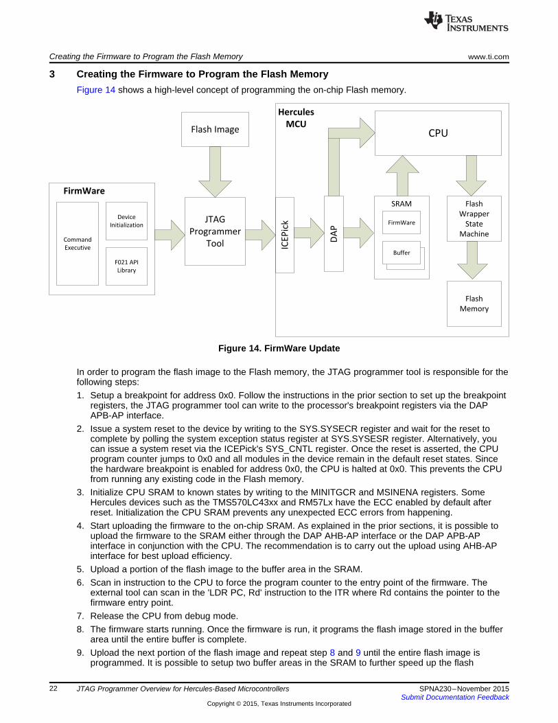
3 Creating the Firmware to Program the Flash MemoryFigure 14 shows a high-level concept of programming the on-chip Flash memory.
Figure 14. FirmWare Update
In order to program the flash image to the Flash memory, the JTAG programmer tool is responsible for thefollowing steps:1. Setup a breakpoint for address 0x0. Follow the instructions in the prior section to set up the breakpoint
registers, the JTAG programmer tool can write to the processor's breakpoint registers via the DAPAPB-AP interface.
2. Issue a system reset to the device by writing to the SYS.SYSECR register and wait for the reset tocomplete by polling the system exception status register at SYS.SYSESR register. Alternatively, youcan issue a system reset via the ICEPick's SYS_CNTL register. Once the reset is asserted, the CPUprogram counter jumps to 0x0 and all modules in the device remain in the default reset states. Sincethe hardware breakpoint is enabled for address 0x0, the CPU is halted at 0x0. This prevents the CPUfrom running any existing code in the Flash memory.
3. Initialize CPU SRAM to known states by writing to the MINITGCR and MSINENA registers. SomeHercules devices such as the TMS570LC43xx and RM57Lx have the ECC enabled by default afterreset. Initialization the CPU SRAM prevents any unexpected ECC errors from happening.
4. Start uploading the firmware to the on-chip SRAM. As explained in the prior sections, it is possible toupload the firmware to the SRAM either through the DAP AHB-AP interface or the DAP APB-APinterface in conjunction with the CPU. The recommendation is to carry out the upload using AHB-APinterface for best upload efficiency.
5. Upload a portion of the flash image to the buffer area in the SRAM.6. Scan in instruction to the CPU to force the program counter to the entry point of the firmware. The
external tool can scan in the 'LDR PC, Rd' instruction to the ITR where Rd contains the pointer to thefirmware entry point.
7. Release the CPU from debug mode.8. The firmware starts running. Once the firmware is run, it programs the flash image stored in the buffer
area until the entire buffer is complete.9. Upload the next portion of the flash image and repeat step 8 and 9 until the entire flash image is
programmed. It is possible to setup two buffer areas in the SRAM to further speed up the flash
22 JTAG Programmer Overview for Hercules-Based Microcontrollers SPNA230–November 2015Submit Documentation Feedback
Copyright © 2015, Texas Instruments Incorporated
www.ti.com Flash Verification
programming process. While one buffer area is being programmed to the Flash memory, theprogrammer tool can upload the next portion of the flash image in the second buffer area in parallel.
4 Flash VerificationTexas Instruments distributes the Flash programming algorithms (see [7]) to customers and third partiesas pre-compiled object libraries. The library is linked into the customers project ensuring that the FLASHprogramming object code will be the same as that validated by TI. However, it is still possible that theapplication program does not use the FLASH API functions correctly by either passing incorrect values orusing the functions in a manner not in accordance with the API documentation. In order to ensure properusage of the Flash API, the application programming must be validated. For details, see [6] on flashvalidation and profiling.
5 References1. TI ICEPick TAP Router Module Type C (SPRUH35)2. CoreSight Components Technical Reference Manual (DDI0314H_coresight_components_trm.pdf)3. Cortex-R4 and Cortex-R4F Revision: r1p4 Technical Reference Manual
(DDI0363G_cortex_r4_r1p4_trm.pdf)4. Router (ICEPick-C) Debug Configuration Information (Router_Scan_Sequence.pdf)5. Tools For Debugging JTAG and Power Issues on DaVinci and OMAP devices (SPRP603)6. F021 Flash API Validation and Update Procedure User's Guide (SPNU609)7. F021 Flash API Version 2.01.01 Reference Guide (SPNU501)
23SPNA230–November 2015 JTAG Programmer Overview for Hercules-Based MicrocontrollersSubmit Documentation Feedback
Copyright © 2015, Texas Instruments Incorporated

IMPORTANT NOTICE
Texas Instruments Incorporated and its subsidiaries (TI) reserve the right to make corrections, enhancements, improvements and otherchanges to its semiconductor products and services per JESD46, latest issue, and to discontinue any product or service per JESD48, latestissue. Buyers should obtain the latest relevant information before placing orders and should verify that such information is current andcomplete. All semiconductor products (also referred to herein as “components”) are sold subject to TI’s terms and conditions of salesupplied at the time of order acknowledgment.TI warrants performance of its components to the specifications applicable at the time of sale, in accordance with the warranty in TI’s termsand conditions of sale of semiconductor products. Testing and other quality control techniques are used to the extent TI deems necessaryto support this warranty. Except where mandated by applicable law, testing of all parameters of each component is not necessarilyperformed.TI assumes no liability for applications assistance or the design of Buyers’ products. Buyers are responsible for their products andapplications using TI components. To minimize the risks associated with Buyers’ products and applications, Buyers should provideadequate design and operating safeguards.TI does not warrant or represent that any license, either express or implied, is granted under any patent right, copyright, mask work right, orother intellectual property right relating to any combination, machine, or process in which TI components or services are used. Informationpublished by TI regarding third-party products or services does not constitute a license to use such products or services or a warranty orendorsement thereof. Use of such information may require a license from a third party under the patents or other intellectual property of thethird party, or a license from TI under the patents or other intellectual property of TI.Reproduction of significant portions of TI information in TI data books or data sheets is permissible only if reproduction is without alterationand is accompanied by all associated warranties, conditions, limitations, and notices. TI is not responsible or liable for such altereddocumentation. Information of third parties may be subject to additional restrictions.Resale of TI components or services with statements different from or beyond the parameters stated by TI for that component or servicevoids all express and any implied warranties for the associated TI component or service and is an unfair and deceptive business practice.TI is not responsible or liable for any such statements.Buyer acknowledges and agrees that it is solely responsible for compliance with all legal, regulatory and safety-related requirementsconcerning its products, and any use of TI components in its applications, notwithstanding any applications-related information or supportthat may be provided by TI. Buyer represents and agrees that it has all the necessary expertise to create and implement safeguards whichanticipate dangerous consequences of failures, monitor failures and their consequences, lessen the likelihood of failures that might causeharm and take appropriate remedial actions. Buyer will fully indemnify TI and its representatives against any damages arising out of the useof any TI components in safety-critical applications.In some cases, TI components may be promoted specifically to facilitate safety-related applications. With such components, TI’s goal is tohelp enable customers to design and create their own end-product solutions that meet applicable functional safety standards andrequirements. Nonetheless, such components are subject to these terms.No TI components are authorized for use in FDA Class III (or similar life-critical medical equipment) unless authorized officers of the partieshave executed a special agreement specifically governing such use.Only those TI components which TI has specifically designated as military grade or “enhanced plastic” are designed and intended for use inmilitary/aerospace applications or environments. Buyer acknowledges and agrees that any military or aerospace use of TI componentswhich have not been so designated is solely at the Buyer's risk, and that Buyer is solely responsible for compliance with all legal andregulatory requirements in connection with such use.TI has specifically designated certain components as meeting ISO/TS16949 requirements, mainly for automotive use. In any case of use ofnon-designated products, TI will not be responsible for any failure to meet ISO/TS16949.
Products ApplicationsAudio www.ti.com/audio Automotive and Transportation www.ti.com/automotiveAmplifiers amplifier.ti.com Communications and Telecom www.ti.com/communicationsData Converters dataconverter.ti.com Computers and Peripherals www.ti.com/computersDLP® Products www.dlp.com Consumer Electronics www.ti.com/consumer-appsDSP dsp.ti.com Energy and Lighting www.ti.com/energyClocks and Timers www.ti.com/clocks Industrial www.ti.com/industrialInterface interface.ti.com Medical www.ti.com/medicalLogic logic.ti.com Security www.ti.com/securityPower Mgmt power.ti.com Space, Avionics and Defense www.ti.com/space-avionics-defenseMicrocontrollers microcontroller.ti.com Video and Imaging www.ti.com/videoRFID www.ti-rfid.comOMAP Applications Processors www.ti.com/omap TI E2E Community e2e.ti.comWireless Connectivity www.ti.com/wirelessconnectivity
Mailing Address: Texas Instruments, Post Office Box 655303, Dallas, Texas 75265Copyright © 2015, Texas Instruments Incorporated