Technology - MOS Electronic · 2014-08-03 · MOS Electronic GmbH Hermann-Loens-Straße 40-44...
49
printed circuit board technology for the future Technology by MOS
Transcript of Technology - MOS Electronic · 2014-08-03 · MOS Electronic GmbH Hermann-Loens-Straße 40-44...

MOS Electronic GmbHHermann-Loens-Straße 40-44D-75389 Neuweiler
phone +49 (0) 70 55 - 92 99 -0 | fax +49 (0) 70 55 - 15 [email protected] | www.mos-electronic.de printed circuit board technology for the future
Technologyby MOS
7th
editi
on, D
ate
of is
sue:
Nov
embe
r 201
3Te
chno
logy
by
MO
S
Technology by MOS7th edition, Date of issue: November 2013
Table of contents
8 - 9
10 - 12
13
13
14
15
15
16 - 17
18
18
19 - 20
21
22 - 27
222324252627
28
29
30 - 31
About MOS
The MOS Group
Express Service
PoolPlus
Designs
Service and advice
Formats
Base materials
Layer structures
Impedance test
Impedance models
Layer structure withimpedance-controlled conductors
Design rules
- External layers - Internal layers - Boreholes and microvias - HDI / SBU design - Coatings and screen printing - Mechanical
Soldermask
Lacquers / Printing / Coatings
Final surfaces / Coatings
Table of contents
32 - 34
34
35 - 41
3637
41
42 - 52
44484950
53 - 83
5354 - 5960 - 7273 - 79
80 - 8283
84 - 85
86
87
90 - 93
Via filling
Copper hole filling
Press-fit technology
- Flexible or elastic press-fit technology - Solid press-fit technology
Thick copper & backplanes
IMS
- Materials - Versions - The single-layer IMS board - Multiple-layer IMS versions
Flex-rigid technology
- Applications - Base materials - Design information - Procedure (example of a 2-layer
flex-rigid with ZIF-connector) - Error patterns - Description of drilling geometry
Environmental protection
Contact
Agents
Notes
Prepreg
SBUcore
Prepreg
Stacked blind via
Fille
din
tern
alpl
td b
oreh
ole
Fille
din
tern
alpl
td b
oreh
ole
Stacked blind via
i

Qualityby MOS
9
About MOS
8
MOS Electronic has almost three dec-ades of experience in the production of printed circuits. Cooperation with our partners in the Far East enables us to supply all types of printed circuit boards in any quantity. From proto-types to mass production -
All from a single source
The process of developing prototypes often results in requirements which do not actually apply until mass pro-duction starts a long time later.Our claim that we are "always one step ahead" ensures that your projects to-day feature the technology of tomor-row. After all, our slogan is:
Printed circuit board technologyfor the future
The quality standards of our products are an integral part of our corporate philosophy. Ever since the company was founded it has been our aim to maintain production at the highest possible technological standard. Con-tinuous new investments and product improvements are one of the main rea-sons behind our success.
Our express service was first launched at MOS in 1985. Express production jobs for prototypes but also for emer-gency production of large quantities and deliveries straight to the assembly belt have long been part of our eve-ryday work - all in standard quality of course. Our wide range of references,
for example from the motor industry, document our absolute reliability and professionalism, supported by our extremely flexible team composed of around sixty employees, most of whom have been with us for years.
As a result of our experience and competence as a printed circuit board specialist we are also able to manu-facture even complex products at our contract partners in the Far East. Our familiarity with their production sys-tems and process enable us to create solutions for the cost-optimised mass production of critical products as early as the sample phase, working close with our partners.
ISO 9001:2008
printed circuit board technology for the future

Precision
Flexibility
Quality
Speed
High tech
MOS is on site in China
MOS retains responsibility for quality
Productionin China
Transport & LogisticsOrganisation by MOS
Rework facility / Facilityfor emergency production
Delivery /Warehousing
Full final inspectionby MOS
The MOS Group
Take advantage of our long term experience with mass manufacturers from the Far East. We will take care of all the organisation for you:
Inquiry Production selection Quotation
Order Data preparation Technical clarification
Before we deliver any products to our customers all the consignments from our partners are subjected to extensive receiving inspection and testing procedures.These cover at least the following points:
• Verification and validation of the products and the requisite documents against customer specifications
• Random testing: - Testing the quality of the through-contacts - Checking the mechanical dimensions- Layer thickness measurements (layer structure, copper, Ni/Au, tin, etc.)
• Archiving all documents including reserve samples and test documentation• Special action if requested by customers
The MOS Group
We have been working with specific Asian mass manufacturers since 2005 which now enables us to supply printed circuit boards in all standard sizes. As a result of our experience and compe-tence as a printed circuit board spe-cialist we are also able to manufacture
even complex products at our contract partners in the Far East. Our familiarity with their production systems and proc-ess enable us to create solutions for the cost-optimised mass production of critical products as early as the sample phase, working close with our partners.
1110

"Express services starts with a quotation."• Production within just one working day
- Lead time for HDI and flex-rigid by agreement• Production in standard quality
- Identical processes and machines- Identical IT and archiving- Transferability to mass production
• No restriction to PCB design• Our major strength: Emergency production even for large batches• Flexibility is a matter of course to us -
for important orders even at weekends...
Do you require low cost samples in standard quality as quickly as possible?Try our PoolPlus service.
Have we caught your interest? Why not request our PoolPlus flyer today. Email: [email protected] or by phone from Mr Jens Rosen on phone +49 (0) 70 55 - 92 99 -33.
Express Service
Pool Plus
The MOS Group
Our manufacturers are at least certified to ISO 9001, TS 16949 and ISO 14001. We also have manufacturers for aero-space projects with AS9100 and Nad-cap certification. In addition to products which are fully RoHS-compliant and lead-free processes, generally all prod-ucts are also UL-licensed.
In addition we have also been able to supply UL-licensed products for the Canadian market. We use an extreme-ly professional procedure for selecting our partners. In addition to their clas-sification by technology and batch size, the following factors also play a vital role:
We have at least one "second source" for every technology. During our regu-lar site audits, in addition to qualifica-
tion we also pay increased attention to the company's environmental policy.
Outsourcing
Regularon site audits
Constantquality monitoring
Long termrelationships
Economicalcircumstances
Contractassurance
i1312
Layout and final thicknessConductor width / Spacing 70 µm min.
90 €
Final thickness > 1.00 mm to 2.00 mm +/- 10%
No supplement
Final thickness > 2.00 mm to 3.00 mm +/- 10%
60 €
Final copper thicknessesExternal layers 70 µm (conductor width / spacing 150 µm min.)
No supplement
External layers 105 µm (min. conductor width 140 µm / min. spacing 210 µm) 35 €
Internal layers 70 µm (min. conductor width 140 µm / min. spacing 210 µm)35 €
Internal layers 105 µm (min. conductor width 210 µm / min. spacing 340 µm)50 €
IMS material (aluminium)Thickness 1.00 mm, 1.60 mm or 2.00 mm
No supplement
Final copper thickness 35 µm or 70 µm
No supplement
Thermal conductivity > 1.6 W/m*K (VT4A1) or 2.2 W/m*K (VT4A2)
No supplement
Please note for IMS materials: min. milling diameter: 2.00 mm. Min. hole diameter 1.00 mm.
Supplements may apply if you require complex milling programs or lots of parts on the pool panel.
MechanicsMultiple-up (panel), v-cut
40 €
Multiple-up (panel), milled
60 €
Multiple-up (panel), v-cut + milled
80 €
Please note: our standard mills are 2.0 and 2.4 mm in diameter.
Supplements may apply to thinner mills and complex milling programs.
SurfacesEntek (OSP) / chem. tin (1.0 µm min.) / chem. Ag
40 €
Chem. Ni/Au (3-5 µm Ni / 0.05-0.15 µm Au)
80 €
PrintingLegend ink (silkscreen) on each side (white)
60 €
Legend ink (silkscreen) on each side (not white)
90 €
Peelable mask, per side
90 €
Via-filler
90 €
Carbon printing
120 €
Colour change for solder stop (all colours possible, type: Carapace EMP110) 120 €*
MiscellaneousImpedance test
280 €*
Initial sample inspection report
180 €*
Production to IPC Class 3 (min. hole copper 25 µm)
plus 10% on the total price
Electrical testingElectrical testing for 2 layers and IMS
60 €
Electrical testing for 4 or more layers
included
Number of pool panelsOur offer relates to the size of a pool panel. However, we can also offer two or three pool panels within our
PoolPlus range. The supplements on the total price for one pool panel which we charge for this are as follows:
For 2 pool panels
30%
For 3 pool panels
50%
* The above supplement for multiple pool panels does not apply to these items
We would be delighted to take you order if you wish to take advantage of our offer.
Is your specification not listed? We will be delighted to provide you with a tailored quotation.
Inquiries to: [email protected]
MOS ELECTRONIC GMBH
OPTIONS
LegaL InfOrMaTIOnThe products from the PoolPlus service are supplied by MOS Electronic GmbH. The offer is only valid after the data have undergone a final
review. We reserve the right to refuse unsuitable projects for this offer. Our terms of sale and delivery available at www.mos-electronic.de
are applicable. Prices are quoted exclusive of VAT. Terms of payment: 10 days 2%, 30 days net. Delivery ex-works. If you are interested
or have any questions, please contact our Mr Jens Rosen (Sales, phone 07055-9299-33, [email protected]) or Mr Holdermann (CAM /
Data, phone 07055-9299-38, [email protected]). Please send purchase orders / data to: [email protected]. We will also
be delighted to provide you with a tailored quotation.
Our express service was first launched at MOS
in 1985. Express production jobs for proto-
types but also for emergency production of large
quantities and deliveries straight to the assem-
bly belt have long been part of our everyday work
- all in standard quality of course. Our wide range of ref-
erences, for example from the motor industry, document
our absolute reliability and professionalism, supported
by our extremely flexible team composed of around sixty
employees, most of whom have been with us for years.
As a result of our experience and competence as
a printed circuit board specialist we are also able
to manufacture even complex products at our
contract partners in the Far East. Our familiarity with
their production systems and process enable us to cre-
ate solutions for the cost-optimised mass production of
critical products as early as the sample phase, working
close with our partners. After all, our slogan is:
Valid until 30 June 2013
printed circuit board technology for the future
2 layers 222 € » 4 working days
4 layers 444 € » 6 working days
6 layers 666 € » 8 working days
8 layers 888 € » working days
10
Not fast enough?Ask about our express service options.
2-layer base material
FR 4 TG 140 / (TG 150: supplement 15 €)
Multilayer base material
Isola IS400 (TG 150)
IMS material (aluminium)
Ventec VT4A1 or VT4A2
Final thickness
1.55 mm +/- 10%
Final copper thickness on external layers 35 µm
Final copper thickness on internal layers 18 µm or 35 µm
Surface
HAL lead-free
Solder stop-off
Peters Elpemer 2467 (green matt)
Standard prepegs
1080 / 2116 / 7628
Standard cores (mm)
0.36 / 0.41 / 0.46 / 0.51 / 0.61 / 0.71 / 0.9 / 0.96 (bespoke structure by agreement)
Please note: a symmetrical structure is required.
LAyouTConductor width/Spacing
0.10 mm
Min. residual root solder stop-off
0.10 mm
Final diameter tolerance
• Plated drills < 6.00 mm
+/- 0.10 mm
• Non-plated drills < 6.00 mm
+/- 0.05 mm
• Routing (inner/outer)
+/- 0.10 mmBoreholes over 6.00 mm will be milled
DESIGN
prINtED cIrcuIt boarD
Descriptionour offer is for a pool panel measuring 417 x 570 mm. For smaller
layouts the printed circuit board is reproduced with the best pos-
sible capacity of the available panel. The reproduction is subject to
technical restrictions (spacing from PCB to PCB generally 8 mm).
We guarantee an error-free output volume of at least 60%. If only
one PCB will fit on the pool panel, at least two pool panels must be
ordered (see optional price list). Different layouts per pool panel are
not permitted as part of this offer. All products will be produced to uL
standards and are RoHS-compliant. The production standard is IPC
Class 2 (min. perforated copper 20 µm). Please see our supplement
system for multiple uses and complex milling programs.
Pool panel417 x 570 mm
NEWIMS material (aluminium)
Basic price: 288 €
Lead time: 6 working days
(Subject to material availability)
printed circuit board technology for the future
Pool Plusby MOS
Fast - low cost - Standard qual i ty
• Technological advice• Impedance calculations and layer structure suggestions• Support with the development of new products• Creation of alternative solutions and development to achieve product stability• Use of synergy effects• DFM (design for manufacturing)• Workshops and technology days with bespoke contents
Service and advice
• Standard format for one-sided and double-sided printed circuit boards:580 x 427 mm² (useful area)
• Standard format for multilayer boards:577 x 419 mm² (useful area)
• Standard format for SBU multilayer boards:577 x 419 mm² (useful area)
• Max. size in MOS Group:1200 x 700 mm² (useful area)
• Special sizes available on request
Formats
Designs
• One-sided with up to 50 layers(max. thickness 6 mm, when joined, up to 10 mm, max. 72 layers)
• HDI and SBU multilayers (4 + core + 4 max.)• Blind, buried and microvias• Stacked vias• High frequency and impedance-controlled printed circuit boards• Halogen-free printed circuit boards• Backplanes• Thick copper up to 400 µm• Press-fit technology• IMS / Metal core PCB• Flex / Flex-rigid (also HDI)• Via hole plugging and copper hole filling• Soldermask in various colours• RoHS compliance and UL listing• Special materials (for example Rogers, Nelco, glass-reinforced polyimide, etc.)• Special applications if requested by customers
Our products are manufactured to IPC A600G Class 2 (alternatively Class 3).
1514

Bas
e m
ater
ial (
FR4)
Gra
ce M
TC-9
7N
an Y
a FR
-4-8
6 U
V B
LOC
KIs
ola
IS40
0Ve
ntec
VT-
481
Vent
ec V
T-47
Isol
aPC
L-37
0HR
Use
d fo
rsi
ngle
and
dou
ble-
side
d P
CB
sYe
sYe
sYe
sYe
sYe
sYe
s
Use
d fo
r mul
tilay
er b
oard
s:N
oN
oYe
sYe
sYe
sYe
sTy
pica
l IP
C c
lass
IPC
-410
1C/2
1/2
1/9
7/9
9/1
26/1
26
Fille
rN
ot fi
lled
Not
fille
dIn
orga
nic
Fille
rIn
orga
nic
Fille
rIn
orga
nic
Fille
rIn
orga
nic
Fille
rG
lass
tran
sitio
n te
mpe
ratu
re (T
G)
140°
C14
0°C
150°
C15
0°C
180°
C18
0°C
Del
amin
atio
n tim
e at
260
°C10
min
.15
-25
min
.>
60 m
in.
> 60
min
.>
60 m
in.
> 60
min
.D
elam
inat
ion
time
at 2
88°C
30 s
ec.
2-5
min
.>
5 m
in.
Appr
ox. 2
5 m
in.
> 30
min
.>
30 m
in.
Ther
mal
dec
ompo
sitio
n (T
D)
Appr
ox. 3
05°C
.Ap
prox
. 320
°C.
Appr
ox. 3
30°C
.Ap
prox
. 345
°C.
Appr
ox. 3
55°C
.Ap
prox
. 340
°C.
Exp
ansi
on in
Z d
irect
ion
(bef
ore
TG)
55 p
pm/K
50-7
0 pp
m/K
40-4
5 pp
m/K
45 p
pm/K
45 p
pm/K
35-4
5 pp
m/K
STI
I >21
5N
oN
oN
oYe
sYe
sYe
s
Die
lect
ric c
onst
ant (
εr)
at 1
MH
z4.
74.
74.
8-5.
14.
34.
34.
9-5.
1
Loss
fact
or a
t 1M
Hz
0.01
450.
020.
013-
0.01
80.
015
0.01
50.
012-
0.01
4C
AF
resi
stan
ceN
oYe
sYe
sYe
sYe
sYe
sR
oHS
-com
plia
ntYe
sYe
sYe
sYe
sYe
sYe
sU
L lis
ting
Yes
Yes
Yes
Yes
Yes
Yes
Avai
labi
lity
(not
gua
rant
eed)
From
sto
ckAv
aila
ble
From
sto
ckAv
aila
ble
From
sto
ckAv
aila
ble
Sho
rt le
ad
time
Sho
rt le
ad
time
2 w
eeks
Different applications require different base materials.The following material types are used at MOS:
• Low, mid and high TG FR4• Materials for high frequency applications (for example Rogers, Nelco, etc.)• Halogen-free materials• Polyimide / Glass-reinforced polyimide• Teflon• Ceramic-filled materials• IMS (aluminium, copper, brass, etc.)• Special materials if requested by customers
Base materials are classified by their thermal, electrical and mechanical properties.
Thermal properties• Glass transition temperature (TG)• Delamination time
(at 260°C and 288°C)• Expansion properties
(CTE in x, y, and z)• Resistance in cycle tests• Heat conductivity in W/mK
Mechanical properties• Elasticity• Bending strength
On the following pages we would like to give you more details about the standard materials we use. All the standard materials we use are suitable for lead-free soldering processes. Thermally conductive materials are listed in the special IMS section starting on page 42.
Base materials
Do you have any questions about base materials?Our Technology Team will be delighted to help (see page 86).i
Electrical properties• Dielectric constant (εr)• Comparative tracking index (CTI)• CAF resistance• Surface resistance• Loss angle• Voltage strength
1716

Impedance models
In practice a range of impedance calculation models are used depending on the specific requirements. The following provides details of four commonly used models.
Coated microstripIndividual impedance-controlled conductors on the external layers.
Main factors:- Distance from reference surface (H1)- Printed conductor width (W1)- Dielectric constant (εr) of the
materials used
Edge coupled coated microstripImpedance-controlled conductors in pairs on the external layers.
Main factors:- Distance from reference surface (H1)- Printed conductor width (W1)- Printed conductor spacing (C3)- Dielectric constant (εr) of the
materials used
Offset striplineIndividual Impedance-controlled conductors on the internal layers with two reference surfaces.
Main factors:- Distance from reference surfaces
(H1 and H2)- Printed conductor widths (W1 and W2)- Dielectric constant (εr) of the
materials used
The properties of a printed circuit board are determined not least by its layer structure. The layer structure influences the impedances, for example. The following contains a list of standard prepreg types used by MOS:
• 106• 1080• 2116• 7628
Other types possible on request. The min. core thickness is 50 µm. Total thick-nesses from 0.2 mm to 6.0 mm are possible (10.0 mm when joined).
Layer structures
Impedance test
The impedances on the printed circuit board are primarily determined by the PCB layout, the layer structure and the dielectric constant of the materials used. The customer's impedance defi-nitions are generally checked in terms of their feasibility depending on the oth-
er outline conditions using a calcula-tion system (POLAR) and solutions are suggested if necessary. The tolerances are generally checked with a tolerance of +/-10%. However, tolerances of up to +/-5% are also possible to order.
One factor which may result in undesirable differences in impedances is metallised copper layers (for example on the external layers) since they may feature irregularities in terms of their layer thickness. We recommend that impedance-controlled conductors are used on non-metallising internal layers.
We recommend that symmetrical layer structures are used to prevent pos-sible torsion and curvature.
1918

Example
Layer structure with impedance-controlled conductors
Edge coupled offset striplineImpedance-controlled conductors in pairs on the internal layers with two reference surfaces.
Main factors:- Distance from reference surfaces
(H1 and H2)- Printed conductor widths (W1 and W2)- Printed conductor spacing (S1)- Dielectric constant (εr) of the materi-
als used
Measuring an impedance signal
Impedance models
2120
Do you have any questions about layer structures or impedance testing? Our Technology Team will be delighted to help (see page 86).We will be delighted to provide you with a tailored layer structure suggestion.
i

Please note: These design rules are our standard min/max values (for 18 µm base copper). If the copper thickness is increased or special materials are used the feasibility of the specified values becomes restricted. A review of the production documents is required for a final feasibility assessment.
Printedconductor:
npltdborehole
pltdborehole
BGApad
a
bc
n
k
f
im l
d
e h
g
j
Printedconductor:
npltdborehole
pltdborehole
a
bc
l
i
f
hk j
d
e g
Design rules
Comments
Min. copper thickness (base + galv. copper) 32 μm
Max. copper thickness (base + galv. copper) 400 μm
Conductor width tolerance +/-10%
Min. hole copper20 μm / 25 μm
Others available on request
BGA pad (diameter) 0.3 mm
BGA pad pitch (one conductor between pad/pad) 0.5 mm
BGA pad pitch (two conductors between pad/pad) 0.65 mm
a Min. conductor width 70 μm Sample up to 50 µm
b Min. conductor spacing 70 μm Sample up to 50 µm
c Conductor pitch 140 μm Sample up to 100 µm
d Conductor / Conductor spacing 70 μm Sample up to 50 µm
e Conductor / Via pad spacing 70 μm Sample up to 50 µm
f Conductor / Earth area spacing 70 μm Sample up to 50 µm
g Conductor / BGA pad spacing 70 μm Sample up to 50 µm
h Via pad / Via pad spacing 70 μm Sample up to 50 µm
i Via pad / Earth area spacing 70 μm Sample up to 50 µm
j Via pad / BGA pad spacing 70 μm Sample up to 50 µm
k Earth area / Earth area spacing 70 μm
l Distance between printed conductor and PCB edge
200 μm Special technology up to 50 µm
m Distance between pad and PCB edge 200 μm Special technology up to 50 µm
n Distance between earth area and PCB edge 200 μm Special technology up to 50 µm
Special parameters available on request
Design rules
Comments
Min. core thickness 50 μm
Min. copper lamination 9 μm
Max. copper lamination 400 μm
Conductor width tolerance +/-10%
a Min. conductor width 70 μm Sample up to 50 µm
b Min. conductor spacing 70 μm Sample up to 50 µm
c Conductor pitch 140 μm Sample up to 100 µm
d Conductor / Conductor spacing 70 μm Sample up to 50 µm
e Conductor / Via pad spacing 70 μm Sample up to 50 µm
f Conductor / Earth area spacing 70 μm Sample up to 50 µm
g Via pad / Via pad spacing 70 μm Sample up to 50 µm
h Via pad / Earth area spacing 70 μm Sample up to 50 µm
i Earth area / Earth area spacing 70 μm Sample up to 50 µm
j Distance between printed conductor and PCB edge
200 μm Special technology up to 50 µm
k Distance between pad and PCB edge 200 μm Special technology up to 50 µm
l Distance between earth area and PCB edge 200 μm Special technology up to 50 µm
Special parameters available on request
External layers Internal layers
2322

a
b
eh
g
c
i f
d j
eg
f
d c b
a
Design rules
Boreholes(Laser and mechanical) Feasibility
a Min. hole diameter (pltd) Drilling Ø 0.2 mm / Final Ø 0.15 mm
b Min. Via pad (pltd) Final Ø +0.25 mm
c Min. hole diameter buried via (pltd) Drilling Ø 0.2 mm / Final Ø 0.15 mm
d Min. Via pad for buried vias (pltd) Final Ø +0.25 mm
e Min. via / via spacing (pltd) 0.30 mm
f Min. hole / hole spacing (npltd) 0.15 mm
g Min. via spacing (pltd) / conductor pattern 0.20 mm
h Min. via spacing (pltd) / PCB edge 0.30 mm
h Min. hole spacing (npltd) / PCB edge 0.30 mm
i Min. diameter microvia (layer 1-2) Drilling Ø 0.1 mm / Final Ø 0.05 mm
j Min. via-pad microvia (layer 1-2) Final Ø +0.2 mm
Design rules
HDI / SBU Design Feasibility
Max. sequential structures 4 + core + 4
Min. prepreg thickness for sequential structure PP106 (approx. 50 μm)
Min. diameter microvia Drilling Ø 0.1 mm / Final Ø 0.05 mm
Max. aspect ratio microvia 1:1
a Internal microvias Yes
b Stacked via on through borehole Yes
c Stacked via on microvia Yes
d Copper hole filling for microvias Yes
d Via hole plugging for microvias Yes
e PID Yes
f Microvia layer 1-2(PP2116 / ~100 μm max.) Yes
g Microvia layer 1-3(PP1080 / ~75 μm max.) Yes
Please note: These design rules are our standard min/max values (for 18 µm base copper). If the copper thickness is increased or special materials are used the feasibility of the specified values becomes restricted. A review of the production documents is required for a final feasibility assessment.
View of a section
View of a section
Boreholes and microvias HDI / SBU Design
Do you have any questions about our design rules?Our CAM Team will be delighted to help (see page 86).i
2524

Design rules
Soldermask / Layout printing Feasibility
Soldermask thickness ≥ 16 μm
Min. Edge coverage soldermask ≥ 6 μm
a Min. opening soldermask / BGA pad 50 μm
b Min. opening soldermask / SMD pad 50 μm
c Min. residual root soldermask 75 μm
d Min. opening soldermask Pad + 100 μm
e Min. line thickness for text in soldermask 100 μm
g Min. line thickness for layout printing 100 μm
h Min. registration tolerance for layout printing / conductor pattern 100 μm
i Min. registration tolerance for layout printing / NDK borehole ≤ 3.0 mm 100 μm
Min. registration tolerance for layout printing / NDK borehole ≥ 3.0 mm 150 μm
Registration tolerances Standard Limit values
Pltd borehole to conductor pattern +/-100 μm +/-50 μm
Npltd borehole to conductor pattern +/-150 μm +/-100 μm
Milling for conductor pattern +/-150 μm +/-100 μm
Soldermask to conductor pattern +/-100 μm +/-50 μm
Layout printing to conductor pattern +/-100 μm +/-100 μm
Screen printing to conductor pattern +/-200 μm +/-150 μm
Design rules
Mechanical machining Feasibility
Min. tolerance borehole diameter +/-25 μm
Min. tolerance end hole diameter +/-50 μm
Min. tolerance milling +/-50 μm
a Notch angle (V-cut) 30°
V-cut / Conductor pattern registration tolerance +/-100 μm
b Max. pos. tolerance top / bottom notch +/-50 μm
c Min. tol. residual root for PCB thickness up to 1.2 mm +0.10 / -0.05 mm
c Min. tol. residual root for PCB thickness over 1.2 mm +0.15 / -0.05 mm
d Min. spacing skip notches (with chisel) 0.3 mm
d Min. spacing skip notches (with notch cutter) 15 mm
Notch cutter outlet (depending on notch depth) ~7 mm
e Tolerance PCB thickness Generally +/-10%
ec
a
b Notch / V-cut
V-Cutd
Skip notches
d
Pad
aSpacing
Sol
derm
ask
Soldermask
b
c
BSoldermask
e
R100SoldermaskNDK borehole
ig h
Registration
Residual rootsoldermask
Text style in soldermask
Layoutprinting
Please note: These design rules are our standard min/max values (for 18 µm base copper). If the copper thickness is increased or special materials are used the feasibility of the specified values becomes restricted. A review of the production documents is required for a final feasibility assessment.
Coatings and screen printing Mechanics
Do you have any questions about our design rules?Our CAM Team will be delighted to help (see page 86).i
2726

We use Peters Elpemer 2467 and Carapace EMP110 soldermask from Electra as standard. These coatings are applied by spray.
Various colours are possible and it is also possible to produce multi-coloured PCBs. The coatings can be characterised as follows:
• Photodefinable• Maximum resolution (up to 50 µm)• Aqueous-alkaline developable• TWT cycle resistance (temperature cycle test)• Very good resistance in galvanic and chemical baths• Compatible with lead-free soldering processes• Excellent edge coverage• RoHS compliance and UL listing• Complies with IPC-SM-840 C, Classes H and T
• Soldermask in various colours(Standard: Peters Elpemer 2467 / Electra Carapace EMP110)
• Component printing• Service printing• Soldermask• Carbon printing• Via filler printing• Flux stop coating• Silver conductive coating• Heatsink coating
Soldermask
Soldermask Elpemer 2467 EMP110Temperature shock Classes H and T Class H
Disruptive strength 160 - 190 kV/mm 134 kV/mm
Dielectric constant (εr) at 1MHz 3.7 4
Lacquers / Printing / Coatings
The "Pink Circuit Board"MOS Electronic has been supplying soldermask in every conceivable col-our for many years. ELPEMER SD 2431 HG (magenta colours) supplied by Peters is new at MOS. The initial colour samples caused a great deal of discussion when Peters appeared at the Productronica 2011 exhibition in Munich. "Like our other colours, this product features high colour stability.
The special magenta colour was devel-oped at the request of MOS Electronic. The aim of MOS is to highlight its cor-porate design to an even great extent in its product portfolio. Magenta - a col-our than stands for quality.”(Source: LPinfos 3/2011, customer journal published by the PETERS Group)
Do you have any questions about soldermask?Our Technology Team will be delighted to help (see page 86).i
2928
HAL lead-free (hot air tinning)• Solder bath: HAL-Sn99Ag+• Coating thickness 1-30 µm• Good soldering properties• Lengthy storage life (>12 months)• Not suitable for very fine textures• No bonding capacity• Poor planarity• Storage life: 12 months
Chemical Sn• Process: Atotech (standard) and Ormecon possible• Min. coating thickness 1.0 µm• Good soldering properties• Planar surface• Narrow process window for soldering processes• Restricted storage life• Storage life: 6 months
Chemical Ag• Coating thickness 0.15-0.3 µm• Good soldering properties• Bondable• Planar surface• Low processing temperature (approx. 50°C)• Airtight storage required• Storage life: 6 months
Chemical Ni/Au• Coating thickness 3-5 μm Ni, 0.05-0.2 μm Au (soldering and US Al wire bonding)• Coating thickness 3-5 μm Ni, 0.3-0.7 μm Au (soldering and US Au gold wire
bonding)• Good soldering and bonding properties• Good storage properties• High process temperatures• Storage life: 12 months
Chemical Ni/Pd/Au• Palladium coating thickness 0.1-0.5 µm• Can be soldered and bonded• TS / US wire bonding possible• Wide process window• Good storage properties• Planar surface• High cost• Storage life: 12 months
Organic copper passivation (OSP / Entek)• High planarity• Good storage properties• Low cost• High process temperatures• Non-bondable• Storage life: 6 months
HAL leaded• Coating thickness 1-30 µm• Good soldering properties• Low process temperatures• Good storage properties• Not suitable for very fine textures• Non-bondable• No RoHS compliance• Poor planarity• Storage life: 12 months
Other surfaces• Galvanic gold (for example plug gold)• Galvanic nickel• Soldering paints• Reductive goldOther surfaces to order
Final surfaces / Finishes Final surfaces / Finishes
Do you have any questions about surfaces or finishes?Our Technology Team will be delighted to help (see page 86).i
3130
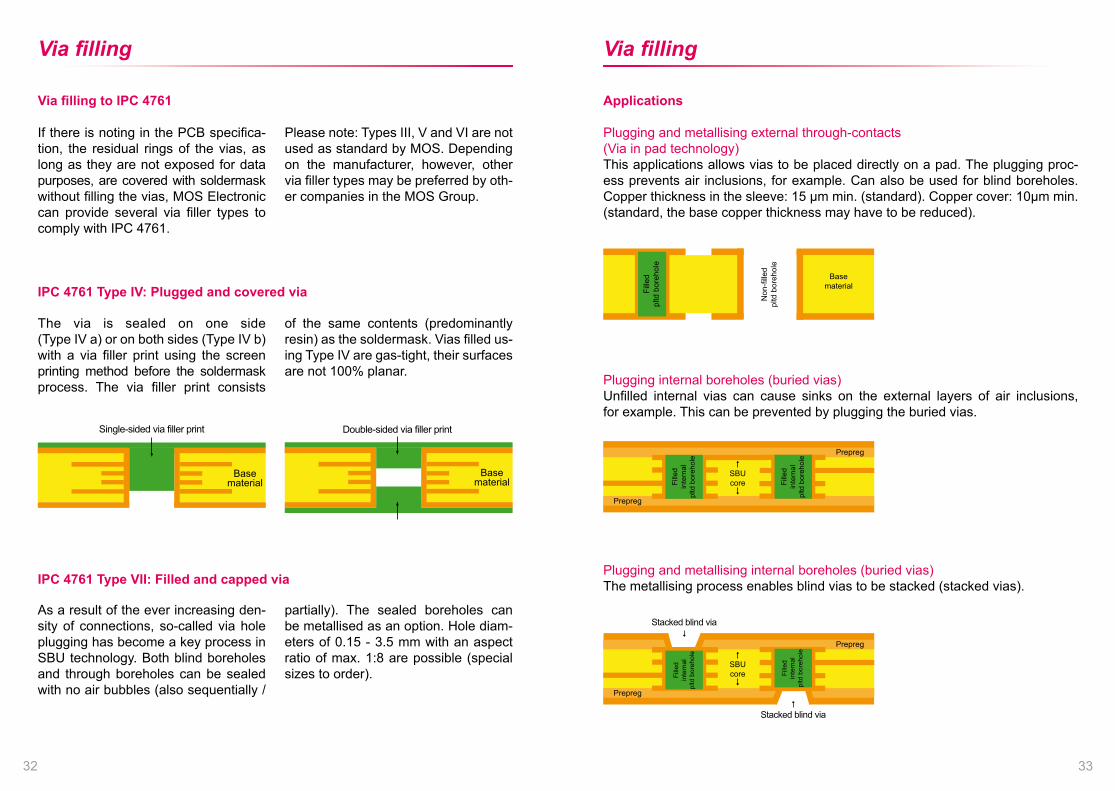
The via is sealed on one side (Type IV a) or on both sides (Type IV b) with a via filler print using the screen printing method before the soldermask process. The via filler print consists
of the same contents (predominantly resin) as the soldermask. Vias filled us-ing Type IV are gas-tight, their surfaces are not 100% planar.
Via filling to IPC 4761
If there is noting in the PCB specifica-tion, the residual rings of the vias, as long as they are not exposed for data purposes, are covered with soldermask without filling the vias, MOS Electronic can provide several via filler types to comply with IPC 4761.
Please note: Types III, V and VI are not used as standard by MOS. Depending on the manufacturer, however, other via filler types may be preferred by oth-er companies in the MOS Group.
Via filling
Single-sided via filler print
Basematerial
Double-sided via filler print
Basematerial
Via filling
Applications
Plugging and metallising external through-contacts(Via in pad technology)This applications allows vias to be placed directly on a pad. The plugging proc-ess prevents air inclusions, for example. Can also be used for blind boreholes. Copper thickness in the sleeve: 15 μm min. (standard). Copper cover: 10μm min. (standard, the base copper thickness may have to be reduced).
Plugging internal boreholes (buried vias)Unfilled internal vias can cause sinks on the external layers of air inclusions, for example. This can be prevented by plugging the buried vias.
Plugging and metallising internal boreholes (buried vias)The metallising process enables blind vias to be stacked (stacked vias).
As a result of the ever increasing den-sity of connections, so-called via hole plugging has become a key process in SBU technology. Both blind boreholes and through boreholes can be sealed with no air bubbles (also sequentially /
partially). The sealed boreholes can be metallised as an option. Hole diam-eters of 0.15 - 3.5 mm with an aspect ratio of max. 1:8 are possible (special sizes to order).
Fille
dpl
td b
oreh
ole
Basematerial
Non
-fille
dpl
td b
oreh
ole
Prepreg
SBUcoreFi
lled
inte
rnal
pltd
bor
ehol
e
Prepreg
Fille
din
tern
alpl
td b
oreh
ole
Prepreg
SBUcore
Prepreg
Stacked blind via
Fille
din
tern
alpl
td b
oreh
ole
Fille
din
tern
alpl
td b
oreh
ole
Stacked blind via
IPC 4761 Type VII: Filled and capped via
3332
IPC 4761 Type IV: Plugged and covered via

A white plugging paste is used for the via hole plugging process.Its properties are as follows:
• Good adhesion between copper and paste even when affected by temperature• Good adhesion of copper, dielectrics and photoresist• No air inclusions in the paste• TG > 140°C• CTE < 50 ppm (below TG)• No shrinkage during curing• Solder bath resistance to IPC-SM-840 C• UL listing, RoHS compliance
We can provide copper-filled blind vias in addition to via filling to IPC 4761. Copper hole filling is possible for hole diameters from 70 μm to 150 μm (microvias, aspect ratio 1:1 max.). The benefits over to via hole plugging are as follows:
• Greater stability• No mechanical stress on the surface (no grinding process)• Copper layer in the sleeve > 25 μm since only one metallising process
is required• Higher TG (TG depends on the base material used)
Via filling
Copper hole filling
Do you have any questions about via filling or copper hole filling?Our Technology Team will be delighted to help (see page 86).i
34
Press-fit technology
Press-fit technology is a technology for solder-free electrical connections be-tween components and printed circuit boards. The press-fit pin is pressed into an interlayer connection borehole. There are two types of press-fit tech-nology which differ by the way in which the press-fit forces are absorbed.
In flexible or elastic press-fit technology the forces are absorbed by the press-fit pin. If solid press-fit pins are used, the retaining force is created by the deformation of the copper sleeve. Both methods produce a gas-tight, electrical connection.
Parameters for the printed circuit board• Drilling or milling tolerances• Tolerance of the final hole diameter• Copper sleeve• Final surface• Thickness of the PCB and copper
thickness
Benefits of press-fit technology• No thermal stress on the printed
circuit board or modules which have already been fitted
• Gas-tight connection• Can be repaired• No solder bridges• No flux residues and therefore
no cleaning required• No additional fastening of the
components required35

Press-fit technology Press-fit technology
Pins with a recess in the press-in zone are used for flexible press-fit technol-ogy. The pin has a larger diameter at this point than the interlayer connection borehole. The recess creates a spring effect which in turn produces the retain-ing force of the press-in connection.
The main criterion for a good press contact for the printed circuit board is primarily the tolerance of the final hole diameter (typically +0.09 / -0.06 de-pending on manufacturer).
The copper sleeve should have a thick-ness of at least 25 µm (possibly plus the final surface, see data sheet from the component manufacturer). Chemi-cal Sn is recommended as the final surface.
Applications For example plug connectors for signal distribution, not for high current applica-tions.
Diameter of the metallised hole Ø 1.60 +0.09/-0.06 mm
min. 25 μm Cu
Flexible or elastic press-fit technology
36
In contrast to flexible press-fit tech-nology the pin is solid (generally with a rectangular or square design). The press-fit pin has a larger circumferential diameter than the interlayer connection
borehole. During the pressing in proc-ess the copper sleeve in the PCB is de-formed which creates the press contact and the gas-tight electrical connection.
Properties• High requirements on the PCB in terms of drilling diameter
(+0.025 / -0.025 mm) and hole copper (min. 30 µm / max. 60 µm)• High current capacity (>300 A)• High resistance to vibrations and dirt• Mechanically more stable compared to solder connections, high
mechanical stresses possible (torques, etc.)
Solid press-fit technology
Würth Elektronikpower elements
Requirements for the printedcircuit board (hole parameters)
Section
Ø 1.60-0,03 min. 0.10
min. 30µm copper max. 60µm
Ø 1.475 ±0.05
The main criterion for a good press contact for the printed circuit board is primarily the tolerance of the borehole diameter before plating and compli-ance with the specified copper thick-ness in the sleeve. Chemical Sn is recommended as the final surface. A single press-fit pin typically has a retaining force of > 100 N.
Example of solid press-fit technology – Würth Elektronik power elements
37

Press-fit technology Press-fit technology
Würth Elektronik is an all-round spe-cialist in press-fit technology. This is backed by more than 25 years of ex-pertise, lots of in-house developments, patents and experience in processing all conventional press-in zones from flexible and knurled to square or rec-tangular.
Würth Elektronik supplies a wide range of power elements with press-fit tech-nology. They are used for the supply and distribution of high currents in sys-tems based on printed circuit boards. They are also ideal for use as connec-tion elements for fuses, IGBTs, switch-es and cables on the printed circuit board or as connection elements from PCB to PCB or PCB to housing.
Power elements are available in vari-ous designs whose design and dimen-sions can be configured to suit specific needs. The solid power elements are available in the form of single-piece (PowerOne), two-piece (PowerTwo) or plug-in (PowerRadsok, PowerLamella or PowerBasket) power elements.
The punches PowerPlus and Power-Plus SMD power elements and the flexible PowerFlex power elements round off the range.
Würth Elektronik ICS GmbH & Co. KGIntelligent connecting systems
3938
MOS Electronic GmbH printed circuit boards have been successfully qualified by Würth Elektronik for processing Würth Elektronik power elements. The satisfy the required printed circuit board specifications and have passed the current capacity tests.
Printed circuit boards must satisfy the following specifications for processing power elements from Würth Elektronik: The current capacity of the power ele-ments must always be regarded in the context of the system as a whole since it depends on the design and pin layout
of the power elements and the layout of the printed circuit board. The tests conducted on them showed that, for example, the combination of "2-layer 70 µm final copper PCB" and "Power One, 20 pins, all-round" can withstand currents of up to 300 A.
Specific requirements for the printed circuit boards

Press-fit technology Thick copper & backplanes
Properties• Durable, breakable connection using high current contact elements• High current applications for 100 to 600 A using connection plates allows
current of well over 1000 A to be transferred to the printed circuit board.• High requirements on the PCB in terms of drilling and milling diameter
(+/-0.025 mm) and hole copper (min. 25 µm / max. 45 µm)
The press-fit pins have a round, serrat-ed shape so that the entire contact sur-face area of the copper sleeve is avail-able for contacting purposes. Broxing power clamps for press-fit technology are available in a range of versions. The press-fit boreholes for the B, N and L series can be fully drilled. How-ever, the H and D series require press-fit boreholes with a diameter of up to
22.15 mm which means that they can-not be drilled any further. MOS Elec-tronic has developed a special, reliable process for these requirements which allows compliance with the tolerance and coating thickness requirements to be guaranteed. Chemical Sn (recom-mended), HAL or chemical Ni/Au may be used as the final surface.
Do you have any questions about press-fit technology?Our Technology Team will be delighted to help (see page 86).i
Example of solid press-fit technology - Broxing power clamps
4140
The layer structure and copper distribution play a major role in thick copper applications in terms of dimension stability and preventing delamination. We will be delighted to advise you personally on the subject of product design.
Design rules for thick copper
LAMINATIONBASE COPPER
MIN. CONDUCTOR WIDTH MIN. DISTANCE
70 µm 140 µm 210 µm
105 µm 210 µm 340 µm
140 µm 280 µm 400 µm
210 µm 420 µm 500 µm
400 µm 800 µm 700 µm
Special parameters available on request
Do you have any questions about thick copper and backplanes?Our Technology Team will be delighted to help (see page 86).i
Press-fit elements are often used for applications relating to signal distri-bution, power consumption and high current applications. MOS Electronic has a wide range of productions and
massive experienced in the produc-tion of high compatibility printed circuit boards. The MOS Group (Far East) can also provide all technologies.
Application and capabilities
Product features• Printed circuit board thickness up to 6 mm, up to 10 m within the MOS Group• Copper thicknesses of up to 400 µm are possible• Max. PCB size: 580 x 427 mm (1 and 2 layers) or 577 x 419 mm (multilayer),
1200 x 700 mm within the MOS Group, special sizes available on request.

IMS IMS
Printed circuit boards with a metal core are enjoying increasing popular-ity wherever high temperatures must be dissipated through the PCB, for example for LED and high power ap-plications.
The following rule of thumb applies for LED applications: A rise in operating temperature by 10°C means 50% short-er service life. However a metal core can also be extremely beneficial for high mechanical stresses or high require-ments relating to dimensional stability.
A solid aluminium or copper plate is generally used as the metal substrate.
The surface and hole walls (if neces-sary) of the metal are coated with a lay-er of insulation. Thermally conductive prepregs (which contain ceramic) are generally used as the dielectric. This gives the product high thermal conduc-
tivity (or fast temperature spread) com-bined with good electrical insulation.
The classic version is a single-sided base material with a metal substrate on the underside. However, 2 or multiple-layer versions with interlayer connec-tions are also possible (metal substrate on the inside or outside.
Properties• High thermal conductivity• Low z-axis expansion• High mechanical strength• Low moisture absorption
Benefits of copper over aluminium• The physical properties of copper are better suited to mixed structures
in terms of its coefficient of expansion and elasticity.• Higher thermal and electrical conductivity• Higher voltage strength• Surfaces suitable for soldering can be applied
4342
Bending angle 30° Bending angle 60°
Bending angle 90° Bending angle 180°
IMSIMS
All IMS materials are pressed in-house by MOS, no prefinished materials are used as standard. This ensure maxi-mum flexibility in the material con-figuration. The dielectrics used have heat conductivity values between 1.6 and 4.2 W/mK (for comparison: 0.2-0.4 W/mK on the standard FR 4). Aluminium or copper in thicknesses between 0.4 mm and 3.0 mm (> 3.0 mm
on request) is generally used as the metal substrate, but other substrates such as brass as also possible. Copper is recommended for multiple-layer ap-plications as a result of the "proximity" of the physical properties to the PCB. As a result of high raw material prices and high weight, however, aluminium is typically used.
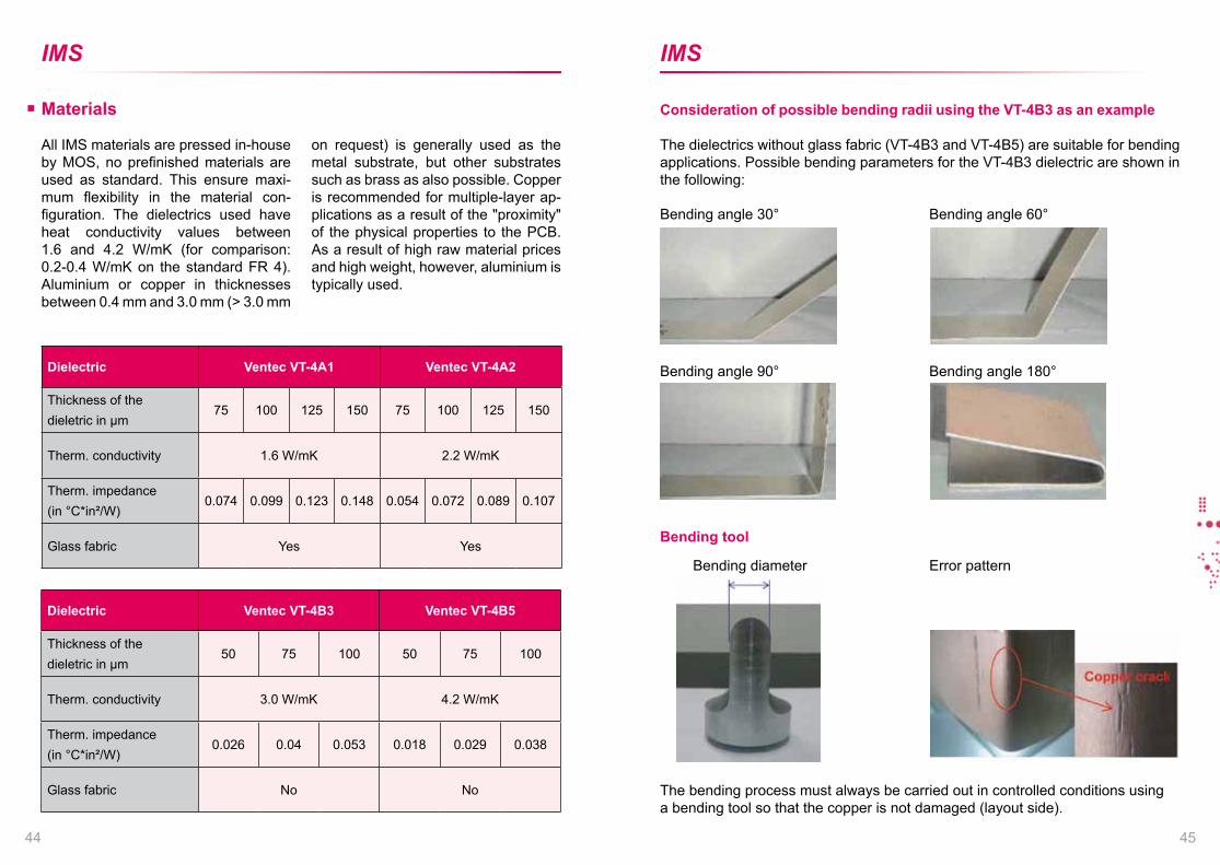
The dielectrics without glass fabric (VT-4B3 and VT-4B5) are suitable for bending applications. Possible bending parameters for the VT-4B3 dielectric are shown in the following:
Materials Consideration of possible bending radii using the VT-4B3 as an example
Dielectric Ventec VT-4A1 Ventec VT-4A2
Thickness of thedieletric in μm
75 100 125 150 75 100 125 150
Therm. conductivity 1.6 W/mK 2.2 W/mK
Therm. impedance(in °C*in²/W)
0.074 0.099 0.123 0.148 0.054 0.072 0.089 0.107
Glass fabric Yes Yes
Dielectric Ventec VT-4B3 Ventec VT-4B5
Thickness of thedieletric in μm
50 75 100 50 75 100
Therm. conductivity 3.0 W/mK 4.2 W/mK
Therm. impedance(in °C*in²/W)
0.026 0.04 0.053 0.018 0.029 0.038
Glass fabric No No
Bending tool
Bending diameter Error pattern
The bending process must always be carried out in controlled conditions using a bending tool so that the copper is not damaged (layout side).
4544

IMSIMS
37
1.0 mm75 μm35 μm
1.0 mm100 μm
35 μm
1.5 mm75 μm35 μm
1.5 mm100 μm35 μm
0.4 mm75 μm35 μm
0.5 mm75 μm35 μm
1.0 mm75 μm35 μm
1.5 mm75 μm35 μm
1.0 mm75 μm35 μm
HTE Super HTE
Bending diameter (mm)
9
8
7
6
5
4
3
2
1
0
AluminiumDielectric
Copper
30°
1.0 mm75 μm35 μm
1.0 mm100 μm35 μm
1.5 mm75 μm35 μm
1.5 mm100 μm35 μm
0.4 mm75 μm35 μm
0.5 mm75 μm35 μm
1.0 mm75 μm35 μm
1.5 mm75 μm35 μm
1.0 mm75 μm35 μm
HTE Super HTE
Bending diameter (mm)
25
20
15
10
5
0
AluminiumDielectric
Copper
60°
1.0 mm75 μm35 μm
1.0 mm100 μm
35 μm
1.5 mm75 μm35 μm
1.5 mm100 μm
35 μm
0.4 mm75 μm35 μm
0.5 mm75 μm35 μm
1.0 mm75 μm35 μm
1.5 mm75 μm35 μm
1.0 mm75 μm35 μm
HTE Super HTE
Bending diameter (mm)
25
20
15
10
5
0
AluminiumDielectric
Copper
90°
1.0 mm75 μm35 μm
1.0 mm100 μm
35 μm
1.5 mm75 μm35 μm
1.5 mm100 μm
35 μm
0.4 mm75 μm35 μm
0.5 mm75 μm35 μm
1.0 mm75 μm35 μm
1.5 mm75 μm35 μm
1.0 mm75 μm35 μm
HTE Super HTE
Bending diameter (mm)
25
20
15
10
5
0
AluminiumDielectric
Copper
180°
4746
IMSIMS
DesignsIn general all technologies which are familiar from conventional printed cir-cuit boards can be used. However, you should know that the metal substrate must initially be insulated for interlayer connections, for example, so as not to short circuit the entire system. There are restrictions for the mechanical ma-chining. Possible special techniques for IMS boards include blind and bur-ied vias, for example. To achieve even better heat dissipation, partial cavities
(cleared or copper and prepreg) may be inserted to connect components which develop high temperature direct to the metal substrate. The component may be connected to the higher cop-per for this technology, for example, using a bonding process. In the event of space problems, deep cuts into the metal substrate may be made and then insulated. Combination with flexible materials is also possible.
Final surfaces• OSP / Entek (recommended)• HAL lead-free / leaded
(do not use HAL for multiple-layer structures)• Chem. Sn• Chem. Ag
• Chem. Ni/Au
Other surfaces available on request
CopperCopper Metal substrateMetal substratePrepreg / Insulation layerPrepreg / Insulation layer
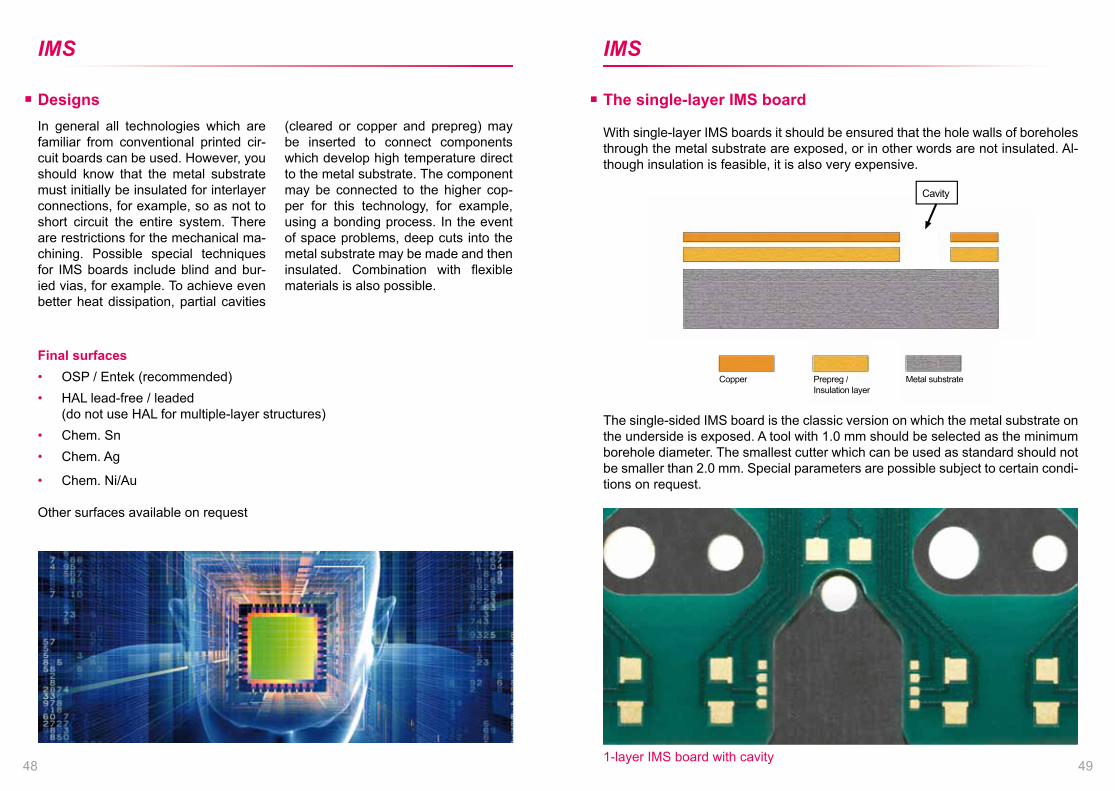
The single-layer IMS board
The single-sided IMS board is the classic version on which the metal substrate on the underside is exposed. A tool with 1.0 mm should be selected as the minimum borehole diameter. The smallest cutter which can be used as standard should not be smaller than 2.0 mm. Special parameters are possible subject to certain condi-tions on request.
1-layer IMS board with cavity
CavityvityCav
With single-layer IMS boards it should be ensured that the hole walls of boreholes through the metal substrate are exposed, or in other words are not insulated. Al-though insulation is feasible, it is also very expensive.
4948
CopperCopper Metal substrateMetal substratePrepreg / Insulation layerPrepreg / Insulation layer
IMSIMS
Multiple-layer IMS versions
ParameterRecom-mended
Limit value
a 1.20 mm 1.00 mmAspect Ratio a Max. 1:1 Max. 1:1
b 0.40 mm 0.30 mmc 0.50 mm 0.30 mmd 1.40 mm 1.20 mmMin. Ø NDK borehole 1.00 mm 1.00 mm
Smallest cutter 2.00 mm 2.00 mm
Special parameters available on request
Section of a metallised borehole with an insulation layer
Prepreg
Cu sleeve
Insulationlayer
Aluminium
a b
c
d
To enable multiple-layer IMS versions to have interlayer connections without con-necting the metal substrate, a layer of insulation should be applied to the hole walls after the preceding drilling process. The actual interlayer connection can be made after the layer of insulation has been applied. The following parameters must be used for the printed circuit board design:
Examples of multiple-layer structures
2-layer structure with metal core
2-layer structure with external metal substrate acting as heat conduction plate
1-layer flexible printed circuit board with metal reinforcement
4-layer structure with metal core
Copper PolyimidPolyimidCopper Adhesive Metal substrateMetal substrate FR4FR4Prepreg / Insulation layerPrepreg / Insulation layer
Legend
5150
IMS
Other heat dissipation methodsIn addition to using IMS materials, there are other methods of dissipating heat.• Radiation• Convection• Heat conduction (external coolers, heatsinks, copper inlays, heat dissipation
through thick copper or thermal vias)
The range of versions can also be combined.
Do you have any questions about IMS boards?Our Technology Team will be delighted to help (see page 86).i
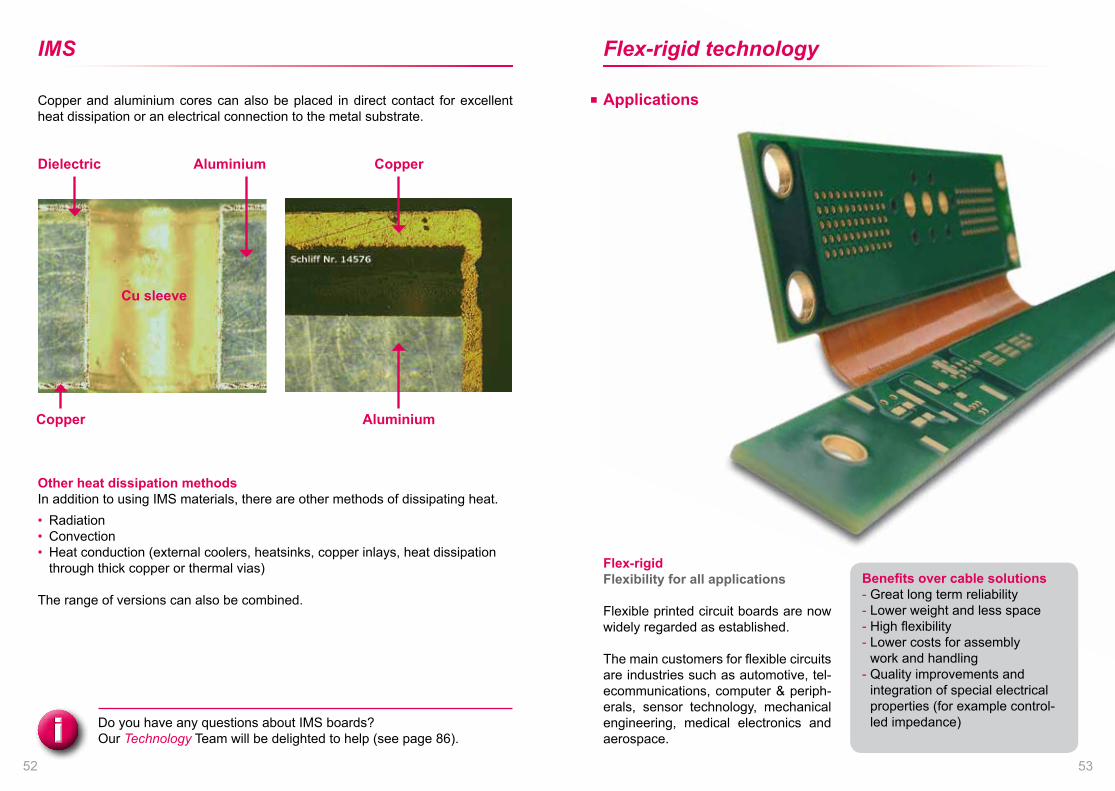
Copper and aluminium cores can also be placed in direct contact for excellent heat dissipation or an electrical connection to the metal substrate.
Dielectric
Copper
CopperAluminium
Aluminium
Cu sleeve
Flex-rigid technology
Benefits over cable solutions- Great long term reliability- Lower weight and less space- High flexibility- Lower costs for assembly
work and handling- Quality improvements and
integration of special electrical properties (for example control-led impedance)
Flexible printed circuit boards are now widely regarded as established.
The main customers for flexible circuits are industries such as automotive, tel-ecommunications, computer & periph-erals, sensor technology, mechanical engineering, medical electronics and aerospace.
Flex-rigidFlexibility for all applications
Applications
5352
Flex-rigid technology Flex-rigid technology
PET: Low price, very restricted soldering capacity, operating temperature approx. -70°C to +70°CPEN: Low price, very restricted soldering capacity, operating temperature approx. -70°C to +90°C PI: High temperature stability, unrestricted soldering capacity, operating temperature approx. -70°C to +110°C, up to 200°C briefly
The following materials are mainly used as base foils:PET (polyethylene teraphthalate)PEN (polyethylene naphtalate)PI (polyimide)*
Selection of materials relative to:- Flexible material- Adhesion- Type of adhesion
(no-flow prepreg, epoxy or acrylic adhesive)
- Temperature stress- Cleaning before interlayer
connection (plasma)- Chemicals for the interlayer
connection process- Design of the layer structure
Quality criteria for flex-rigid printed circuit boards
To ensure that a flex-rigid PCB can become a high quality product, atten-tion must be given to the main quality criteria as early as the design phase (for example selection of base materi-als, information about layout. etc.).
Selection criteria
* preferred
Base foil
Dielectric constant
Disruptive strengthin V/μm
Max. operating temperature
in °C
TGin °C
waterabsorption
in %
Expansionin ppm
PET 3.20 240 105 78 < 0.08 120
PEN 3.16 275 160 120 0.60 65
PI 3.50 204 200 410 > 3.00 70
Properties of the main flexible base foils
Base foil Adhesionin N/cm2
Shrinkage afteretching in %
Water absorptionin %
Flexible base material (PI) > 7 0 - 0.20 < 3
Rigid base material (FR4) 14 0 - 0.02 0.50
Differences between rigid and flexible materials
Comparison of selected properties of the main flexible base foils
- Standard foil thicknesses- Copper thicknesses and types- Adhesives and coatings
Technical data / Differences of flexible materialsBase materials
5554

Flex-rigid technology Flex-rigid technology
Material Thickness in mm
Copper 0.018 0.035 0.070 0.105
Adhesive 0.015 0.025 0.025 0.025
Polyimide 0.025 0.050 0.075 0.125
Copper on one side
Material Thickness in mm
Copper 0.018 0.035 0.070 0.105
Adhesive 0.015 0.025 0.025 0.025
Polyimide 0.025 0.050 0.075 0.125
Adhesive 0.015 0.025 0.025 0.025
Copper 0.018 0.035 0.070 0.105
Copper on two sides
Material Thickness in mm
Copper 0.018 0.035 0.070
Polyimide 0.025 0.050 -
Copper 0.018 0.035 0.070
Copper on two sides, no adhesiveAP material
Standard foils
CopperED: Elongation at rupture 8 – 10% (HTE Cu approx. 16%)RA: Elongation at rupture > 10% (IPC-CF-150 approx. 16%)
AdhesiveEpoxy, acrylic
Flexible base material without adhesive*- AP 9121 (DuPont)- A2010RD (Thinflex) - preferred
Sections
Flexible base material with adhesive- LF 9121 (DuPont)
Polyimide with acrylic adhesive is ideal for dynamic stresses for up to 40 mil-lion bending cycles with the appropri-ate layout and bending radius.
Polyimide with flame-inhibiting adhesive (FR4) is UL 94 VTM -0 listed and certi-fied to IPC Class 2 but only has limited dynamic flexibility. Polyimide without ad-hesive is also UL 94 VTM -0 listed and certified to IPC Class 3. Its temperature resistance is specified at 1,000 hours at 150°C and it also has good chemical re-sistance and low gassing.
* preferred
5756

Parameters- Temper for 2 hours at 120°C in a convection furnace
(store printed circuit boards with gaps between them)- The max. holding time between tempering and the
soldering process is 8 hours. If the holding time exceeds 8 hours a fresh tempering processing is required before the soldering process.
- For reflow soldering processes the max. temperature is 270°C
Flex-rigid technology Flex-rigid technology
Material Thickness in mm
Polyimide 0.025 0.050 0.075 0.125
Adhesive from 25 – 75 µm
Backing foil Removed after mechanical machining
Cover foil
MOS prefers Coverlay from DuPont
So-called flexible coatings (flexible soldermask, for example Peters type 2463) are also used.
Low cost PET material can be used in cases where a flexible PCB is used as a pure connecting element between two connectors and not soldered with normal standard soldering systems. PEN or polyimide must be used as soon as SMD components must be fitted and soldered automatically. The decisive criterion in this respect is the machine equipment and the solder you plan to use. PEN can be used with suit-able machines and automatic solder-ing. Polyimide has a clear advantage in this case. This material is suitable for all standard leaded and unleaded
soldering processes (wave soldering, manual soldering and vapour phase soldering).
It is often the adhesive system in the flexible base materials which deter-mines with flexible PCBs (made of PEN or polyimide) are suitable for use in the field in high temperatures.
The stresses to which flexible PCBs are exposed in the field and during processing determine the choice of the base material.
Selection of materials relative to:- Temperature stress- Requirement for UL listing- Bending stress- Puncture resistance
Flexible coating
?!What does this mean for processing flex-ible circuits?
Since this property has been known for at least 20 years, all processing business have adjusted to it.Polyimide is hydroscopic and there-fore absorbs moisture (water). When this water is heated to over 100°C it turns to water vapour and therefore requires a considerably large volume. If it is heated very quickly (soldering process) this may result in the vapour pressure destroying the adhesion be-tween the various layers (polyimide, adhesive and copper) - in other words delamination.This means that the product must be dried (tempering process) before the soldering process. After drying the PCBs must be processed within 2 - 6 hours or placed in temporary storage in a dry place.
As a result of the high moisture ab-sorption of polyimide the PCBs must be dried (using a tempering process) before the soldering process.
Processing instructions (tempering process)
Drying flexible PCBs made of poly-imide As the diagram shows, polyimide absorbs up to 3% water from the surrounding atmosphere.
Coating thickness (µm)
Insulation voltages
At max.water content
Polyimide foil 2 x 10² V/cm
Polyimide foil 1,5 - 2,5 x 10² V/cmPolyester foil 3 x 10² V/cm
Glass fibre epoxy foil 2,5 x 10² V/cm
100,2
0,5
1,0
2,0
5,0
10
20
20 50 75 100 200
Pun
ctur
e vo
ltage
(kV
)
Do you have any questions about flexible coatings?Our Technology Team will be delighted to help (see page 86).i
5958

Flex-rigid technology Flex-rigid technology
Design information
Layout design (conductive pattern)
Flexible PCBs are used for a wide range of purposes and in many ap-plications they are stressed dynami-cally with up to several million bending cycles. In many other cases flexible PCBs are installed in miniature hous-ings with minimal bending radii. The conductor layout is expected to be able to withstand all these stresses without suffering damage.
If certain basic rules are observed dur-ing the creation of a layout, this sets in place an important foundation for the successful use of flexible PCBs.
Examples
Conductor connectors at soldering eyes should always be droplet shaped and rounded. As large a soldering eye area as possible will help to anchor the soldering eyes on the flexible base ma-terials better.
Soldering eyes which are too small have a poor connection to the flexible base material. This may result in the solder-ing eyes peeling off the base material. A conductor fracture at the transition be-tween the soldering eye and conductor is possible if the conductor connection is very narrow and subjected to stress.
If the layout is designed correctly the soldering eye areas should be as large as possible to ensure that the cover foil or coating covers the soldering eye. This is particularly necessary on 1-lay-er flexible PCBs. On 2-layer interlayer connectors PCBs the soldering eyes are connected from the top to the bot-tom by the interlayer connection sleeve like a rivet and thus well secured.
Soft transitions from narrow to wide conductors are the best way of ensur-ing conductor structures which are no sensitive to fracturing.
Sharp corners in the etched conductor act like a notch in metal. If a compo-nent of this type is bent, the should in the conductor could become an obvi-ous place to fracture.
The transition from narrow to wider conductors at a 90° angle should al-ways be achieved using adequately large radii.
6160

Flex-rigid technology Flex-rigid technology
Here, too, the sharp edges in the 90° angle act like notches in metal. There is a risk of fractures at these point if the component is bent.
If SMD components are fitted to flexible PCBs it is advisable to reinforce these zones with 0.125 mm polyimide foil or 0.5 mm FR4. This prevents the compo-nent zone being bent which may dam-age the soldering points.
Conductor connections to SMD pads must be as far removed from the bend-ing zone as possible. SMD pads are extended under the cover foil to pro-vide better anchoring. 90° conductor kinks are allowed in this zone since they are reinforced with polyimide or FR4. SMD pads are only designed in nominal form in this layout which means that no additional anchoring is achieved. The bending zone (yellow) is too close to the SMD pads which means that there is a very great risk of fractures at the conductor connection to the two right-hand SMD pads.
If flexible PCBs are slit, for example to bend two flexible arms in different directions, an additional copper track must be fitted both for a zero cut (left picture) and for a slit (right picture) to prevent tearing. The zero cut should also end in a borehole. The internal corners of the slit must be as large as possible in the form of a radius. These precautions prevent the flexible PCBs tearing at the points described when subjected to mechanical stresses.
Minimum web width between the gaps: 0.08 mm
Soldermask gap
PadBorehole
Coating web width0.08 mm
Layout parameters
x
Soldermask gap
PadBorehole
x + 0.1Soldermask to conductor pattern:0.15 mm
Parameters for flexible soldermask
Cover foil gap(borehole)
Flow up to 25 µm at 50 µmadhesive thickness(Standard)
Adhesive flowafter lamination
Cover foil
Borehole
Soldering eye
Parameters for cover foils (Coverlay)
6362

Flex-rigid technology Flex-rigid technology
{
Flexible zone Cover foil
Rigid zone Rigid zone
{ {Offset for tacking the cover foil
Tolerance ± 0.25 mm
Tolerance ± 0.25 mm
An adhesive flow occurs during the lamination of cover foils. The adhesive flow is transparent and therefore not al-ways visible.
It is not possible to provide a cover with a final surface in this zone and it must therefore be included in the resid-ual ring design. See diagram entitled "Parameters for cover foils (Coverlay)"
Cover foil
Partial cover foilWhen tacking the cover foil on to flex-ible materials marks for registration are placed outside the PCB contour. This must also be given due consideration in the usage design.
Cover foil webmin. 0.2 mm
RecessCover foil
Solderingeye
Borehole inthe circuit
The cover foil has a backing foil to-wards the adhesive side. When this backing foil is removed and during lam-ination, this web may break and settled on the soldering eye.
Cover foil web width, borehole to borehole
Rigid zone { Rigid zone {Flexiblezone
Sol
derm
ask
Sol
derm
ask
{
Partial cover foil0.8 mm
0.4 mm 0.4 mm
0.8 mm
Partial cover foil and partial solder-mask
The partial cover foil overlaps the soldermask applied previously.Set back the soldermask by at least 0.4 mm from the transition edge.
There must be no interlayer connected boreholes or soldering eyes in the overlap zone. Overcoating or coverage is not permitted.
Cover foil overlap in the rigid zone
Flexible zone{
Cover foilAdhesive
Polyimide
FR 4
No-flowPrepreg
0.8 mm min. overlap
We recommend a web width of at least 0.2 mm to prevent this. If this is not possible the entire zone must be left open (alternatively a flexible solder-mask may be used).
6564

Flex-rigid technology Flex-rigid technology
Cover foil tocustomer’s
drawing
{Rigid zone{
{ {
Rigid zone {Flexible zone
0.8 mm min. overlap
No-flowprepreg
Partialcover foil
No-flow prepreg to level partial cover foil
The cover foil is only partially applied to internal flexibly layers. The other area must be filled with a partial no-flow prepreg to prevent delamination.
Levelling internal cover foil
{Flexible zone withpartial cover foil
No-flow prepreg type 1080(~ 65 μm after pressing)
25 µmcover foil
50 µmadhesive
Zero cut
Pressing(flexible layer)
{ {Flexible zone
1st pressing(flexible layer)
{FR4
Example of a layer structure with internal flexible layer
Flexibilityin every layer
6766

flow
flow
FR4
PolyimideNo-flowPrepreg
max. 0.3 mm
Flex-rigid technology Flex-rigid technology
Max. flow of the no-flow prepreg
Max. undercut(withdrawal of the no-flow prepregs)
undercut
undercut
FR4
PolyimideNo-flowPrepreg
max. 0.2 mm
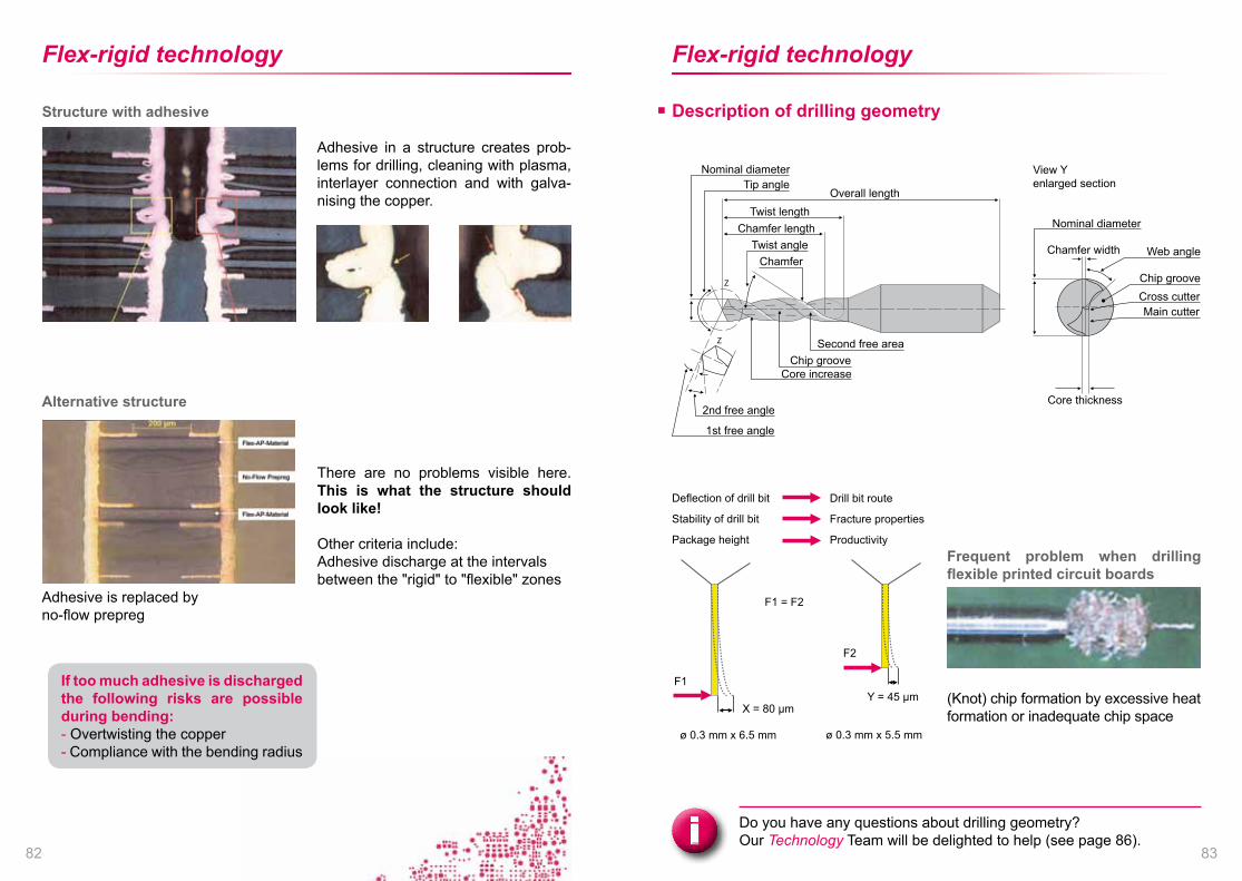
Forward / Counter grooves
Why forward and counter grooves?
Adhesive, no-flow prepreg or transparent adhesive such as LF0100 / LF0200 or composite adhesive LF0111 / LF0212 only have one flow which can only be stopped by the forward groove.
?!Polyimide
Surface (gold)
Cu base (possibly galv. Cu)
Stiffener
ZIF-connector zone
Thickness 0.3 ± 0.03 mm (overall)
ZIF-connector
Consideration in terms of:- Surface- Reinforcement
Do you have any questions about forward and counter grooves?Our Technology Team will be delighted to help (see page 86).i
6968
Flex-rigid technology Flex-rigid technology
Cold adhesionWarm adhesion
FR4
Scotch 467 /3M foil
FR4
No-flowPrepreg
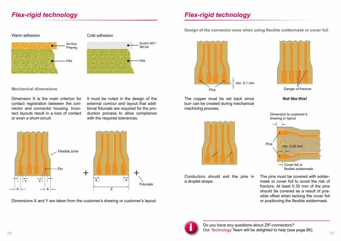
Dimensions X and Y are taken from the customer's drawing or customer's layout.
Flexible zone
Pin
X
Y
X
Y X
+ +
Z
XFiducials
Mechanical dimensions
Dimension X is the main criterion for contact registration between the con-nector and connector housing. Incor-rect layouts result in a loss of contact or even a short-circuit.
It must be noted in the design of the external contour and layout that addi-tional fiducials are required for the pro-duction process to allow compliance with the required tolerances.
Danger of fracture
The copper must be set back since burr can be created during mechanical machining process.
Conductors should exit the pins in a droplet shape.
Not like this!
min. 0.1 mm
Pins
Design of the connector zone when using flexible soldermask or cover foil
The pins must be covered with solder-mask or cover foil to avoid the risk of fracture. At least 0.35 mm of the pins should be covered as a result of pos-sible offset when tacking the cover foil or positioning the flexible soldermask.
Pins min. 0,35 mm
Dimension to customer’sdrawing or layout
Cover foil orflexible soldermask
Do you have any questions about ZIF-connectors?Our Technology Team will be delighted to help (see page 86).i
7170

Flex-rigid technology Flex-rigid technology
Snap-out zone
OK Not OK
With snap-out technology the rigid ma-terial under the flexible zone initially re-mains connected to the rigid section of the PCB and is not removed until the customer receives it. This achieves greater stability during the fitting proc-ess.
The forward grooves are inserted as standard. Retaining webs are left when the counter grooves are cut. These must not be positioned in the conduc-tor zone.
Snap-out technology
Procedure
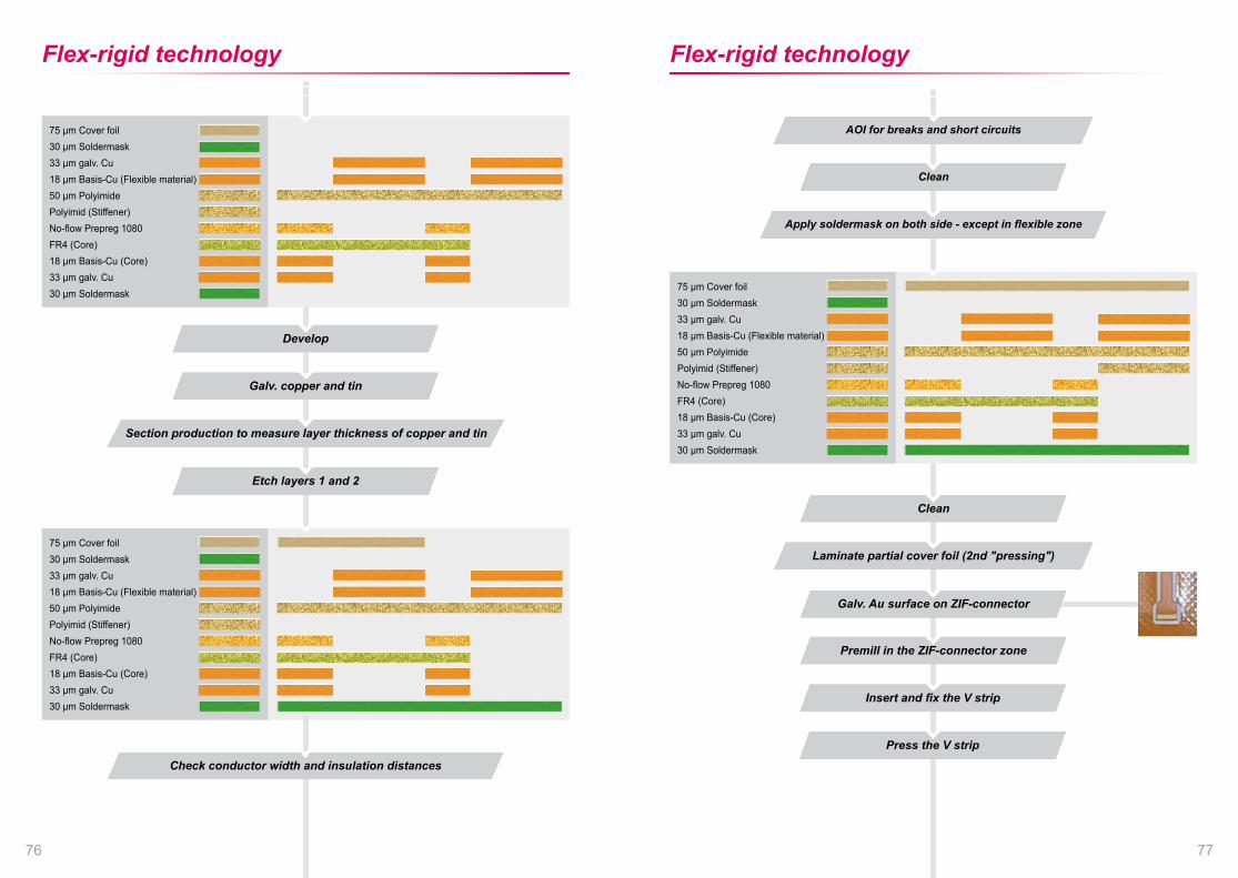
Example of a 2-layer flex-rigid PCB with a ZIF-connector
Material provision
75 µm Cover foil
30 µm Soldermask
33 µm galv. Cu
18 µm Basis-Cu (Flexible material)
50 µm Polyimide
Polyimid (Sti�ener)
No-ow Prepreg 1080
FR4 (Core)
18 µm Basis-Cu (Core)
33 µm galv. Cu
30 µm Soldermask
Production start
Approval of the production data
Production data creation
Check that the input data are complete
Receiving documents
Do you have any questions about snap-out technology?Our Technology Team will be delighted to help (see page 86).i
7372

Flex-rigid technology Flex-rigid technology
Etch Flexible material
75 µm Cover foil30 µm Soldermask33 µm galv. Cu18 µm Basis-Cu (Flexible material)50 µm PolyimidePolyimid (Stiffener)No-flow Prepreg 1080FR4 (Core)18 µm Basis-Cu (Core)33 µm galv. Cu30 µm Soldermask
Expose theCu separating foil
Drill the catch holesand mill therecesses for
the flexible zone
Cut thepartial
Cover foil
Mill theinitial contour
FR4 No-flow prepreg Flexible material Cover foil Stiffener
75 µm Cover foil30 µm Soldermask33 µm galv. Cu18 µm Basis-Cu (Flexible Material)50 µm PolyimidePolyimid (Stiffener)No-flow Prepreg 1080FR4 (Core)18 µm Basis-Cu (Core)33 µm galv. Cu30 µm Soldermask
FR4 / Prepreg / Flexible / Cover foilRecord material charge
Initial pressing
Photo print layer 1 and 2
Clean Cu
Section production
Interlayer connection
Drill
Measure the thickness
75 µm Cover foil30 µm Soldermask33 µm galv. Cu18 µm Basis-Cu (Flexible material)50 µm PolyimidePolyimid (Stiffener)No-flow Prepreg 1080FR4 (Core)18 µm Basis-Cu (Core)33 µm galv. Cu30 µm Soldermask
Clean
Forward groove
Drill catch holes Expose the Cu separating layer
7574
Flex-rigid technology Flex-rigid technology
Check conductor width and insulation distances
75 µm Cover foil30 µm Soldermask33 µm galv. Cu18 µm Basis-Cu (Flexible material)50 µm PolyimidePolyimid (Stiffener)No-flow Prepreg 1080FR4 (Core)18 µm Basis-Cu (Core)33 µm galv. Cu30 µm Soldermask
Etch layers 1 and 2
Section production to measure layer thickness of copper and tin
Galv. copper and tin
Develop
75 µm Cover foil30 µm Soldermask33 µm galv. Cu18 µm Basis-Cu (Flexible material)50 µm PolyimidePolyimid (Stiffener)No-flow Prepreg 1080FR4 (Core)18 µm Basis-Cu (Core)33 µm galv. Cu30 µm Soldermask
Press the V strip
Insert and fix the V strip
Premill in the ZIF-connector zone
Galv. Au surface on ZIF-connector
Laminate partial cover foil (2nd "pressing")
Clean
75 µm Cover foil30 µm Soldermask33 µm galv. Cu18 µm Basis-Cu (Flexible material)50 µm PolyimidePolyimid (Stiffener)No-flow Prepreg 1080FR4 (Core)18 µm Basis-Cu (Core)33 µm galv. Cu30 µm Soldermask
Apply soldermask on both side - except in flexible zone
Clean
AOI for breaks and short circuits
7776

Flex-rigid technology Flex-rigid technology
Production of a section to measure the coating thick-
ness of copper / soldermask / surface and thickness
Inspection / VisualTest 257°C
75 µm Cover foil30 µm Soldermask33 µm galv. Cu18 µm Basis-Cu (Flexible Material)50 µm PolyimidePolyimid (Stiffener)No-flow Prepreg 1080FR4 (Core)18 µm Basis-Cu (Core)33 µm galv. Cu30 µm Soldermask
Electrical test for breaks and short circuit (40 V)
Laser cut the total contour
Initial contour - counter groove outline and remove the cover
75 µm Cover foil30 µm Soldermask33 µm galv. Cu18 µm Basis-Cu (Flexible material)50 µm PolyimidePolyimid (Stiffener)No-flow Prepreg 1080FR4 (Core)18 µm Basis-Cu (Core)33 µm galv. Cu30 µm Soldermask
Test report
Delivery
Shipment inspection
7978

Flex-rigid technology Flex-rigid technology
Error patterns
The copper surface for contacting is coated with a cover foil (50 µm acrylic sticker, 25 µm polyimide). A borehole can only be cleaned by plasma in such a case. The two images show the
result of cleaning a borehole with chemicals. They are not compatible with the acrylic adhesive.
Microvia to contact FR4 to flex
This image shows a strong undercut around the adhesion. This can result in a break if the copper does not 100% cover the undercut. In this case it is completely covered.
Various defects can be seen here.- Nail head in the polyimide- Nail head in the copper- Undercut
The interlayer connection is imperfect due to the bundling of the defects and results in a failure in the electrical test or later in the field.
Examples of poor interlayer connections
Borehole with standard geometry
Borehole with flexible drill geometry
Interlayer connection flaws in the poly-imide zone of a 2-sided flex-rigid PCB
Flaw in the epoxy adhesive zone. This error occurs if the circuit is left in the chemicals for too long.
Examples of poor interlayer connections
Epoxy adhesivePolyimide 50 μm
8180
Flex-rigid technology Flex-rigid technology
There are no problems visible here. This is what the structure should look like!
Other criteria include:Adhesive discharge at the intervals between the "rigid" to "flexible" zones
Alternative structure
If too much adhesive is discharged the following risks are possible during bending:- Overtwisting the copper- Compliance with the bending radius
Adhesive in a structure creates prob-lems for drilling, cleaning with plasma, interlayer connection and with galva-nising the copper.
Structure with adhesive
Adhesive is replaced by no-flow prepreg
Description of drilling geometry
ø 0.3 mm x 6.5 mm ø 0.3 mm x 5.5 mm
F1 = F2
F1
F2
Y = 45 µmX = 80 µm
Deflection of drill bit
Stability of drill bit
Package height
Drill bit route
Fracture properties
ProductivityFrequent problem when drilling flexible printed circuit boards
(Knot) chip formation by excessive heat formation or inadequate chip space
Do you have any questions about drilling geometry?Our Technology Team will be delighted to help (see page 86).i
8382
Z
Z
Nominal diameterTip angle
Overall lengthTwist length
Chamfer lengthTwist angle
Chamfer
Second free areaChip groove
Core increase
2nd free angle
1st free angle
Core thickness
Main cutterCross cutterChip groove
Web angleChamfer width
Nominal diameter
View Yenlarged section
The subject of protecting the environment and preserving resources has been an integral part of our thoughts and actions since the company was founded. Located at the edge of a conservation area in the Northern Black Forest nature reserve, we pay very close attention to saving material, water and energy and to improving our consumption levels.
These factors also play a major role when we are selecting new production equip-ment. The recycling of materials and media has long been a matter of course for us. The subject of the environment is also a significant criterion when we select our group partners.
Our partners are certified to ISO 14001 without exception.
Environmental protection
8584

AgentsContact
We look forward to receiving your inquiries either by phone or to [email protected]
Mrs Elke Lörcher +49 (0) 70 55 - 92 99 -12 [email protected]
Accounts, Purchasing
Mrs Sibylle Klingler +49 (0) 70 55 - 92 99 -13 [email protected]
Mr Andreas Klittich +49 (0) 70 55 - 92 99 -43 [email protected]
Mr Edin Sisic [email protected]
Quality Assurance
Mr Klaus Holdermann +49 (0) 70 55 - 92 99 -38 [email protected]
CAM, Data
Mr Ernst Winkler +49 (0) 70 55 - 92 99 -16 [email protected]
Product Manager Flex-Rigid Technology
Mrs Gabi Walz +49 (0) 70 55 - 92 99 -35 [email protected]
Work Preparation
Mr Michael Klingler +49 (0) 70 55 - 92 99 [email protected]
Mr Matthias Klingler +49 (0) 70 55 - 92 99 [email protected]
Technology & Production
Mr Jens Rosen Sales Manager +49 (0) 70 55 - 92 99 [email protected]
Mr Roland Drexler Sales +49 (0) 70 55 - 92 99 [email protected]
Mrs Sabrina Hammann Support & Logistics +49 (0) 70 55 - 92 99 [email protected]
Sales
Mr Horst Schmalstieg Managing Director +49 (0) 70 55 - 92 99 [email protected]
Mr Reinhard Rosen Managing Director +49 (0) 70 55 - 92 99 [email protected]
Mr Jürgen Bauer Authorised Signatory +49 (0) 70 55 - 92 99 [email protected]
Mrs Margrit Schmalstieg Managing Director +49 (0) 70 55 - 92 99 [email protected]
Management
Head office: +49 (0) 70 55 - 92 99 -0 • [email protected]
Staub Industrievertretungen GmbHMr Rainer StaubObere Torstrasse 6D-72108 Rottenburgphone: +49 (0) 74 57 - 69 72 52fax: +49 (0) 74 57 - 32 92mobile: +49 (0) 160 - 36 55 056mail: [email protected]
HVB Handelsvertretung BeitingerMr Hartmut BeitingerMörikestrasse 5D-74254 Offenauphone: +49 (0) 71 36 - 96 27 880mobile: +49 (0) 172 - 95 49 683mail: [email protected]
Willuweit IndustrievertretungenMr Jürgen WilluweitKesselbergweg 30D-52385 Nideggenphone: +49 (0) 2427 - 909 59-20fax: +49 (0) 2427 - 909 59-21mobile: +49 (0) 1573 - 566 48 41mail: [email protected]
CEE SASC C.E.E.S.R.L.B-dul Industriei nr. 4300714 Timisoara (ROMANIA)mail: [email protected](Contact through MOS)
Karl-Friedrich KempfIndustry AgentsWaldstrasse 56D-77933 Lahr phone: +49 (0) 78 21 - 98 33 26fax: +49 (0) 78 21- 98 33 27mobile: +49 (0) 175 - 16 39 464mail: [email protected]
A/M/T Industry PartnersIndustry AgentsMr Achim TrampenauAckerstrasse 29D-90513 Zirndorfphone: +49 (0) 9127 - 57 04 70fax: +49 (0) 911 - 960 61 38mobile: +49 (0) 174 - 348 95 79mail: [email protected]
A. Arnold ElectronicVertretungs- und Vertriebs GmbHAm Kesseborn 10D-59427 Unnaphone: +49 (0) 23 03 - 40 397fax: +49 (0) 23 03 - 40 391mail: [email protected]
8786


Notes
9190

Notes
9392
We are pink.
the pink circuit board
printed circuit board technology for the future

Legal Information
© 2013 MOS Electronic GmbHHermann-Loens-Strasse 40-44D-75389 NeuweilerProject Manager: Jens Rosen
Layout and designKing DesignAgentur für Werbung und MarketingD-75389 Neuweilerwww.kingdesign-online.de
All rights reserved.This work and all its components are protected by copyright.They must not be used or may only be used with the prior consent of MOS Electronic GmbH.

MOS Electronic GmbHHermann-Loens-Straße 40-44D-75389 Neuweiler
phone +49 (0) 70 55 - 92 99 -0 | fax +49 (0) 70 55 - 15 [email protected] | www.mos-electronic.de printed circuit board technology for the future
Technologyby MOS
7th
editi
on, D
ate
of is
sue:
Nov
embe
r 201
3Te
chno
logy
by
MO
S