TAS5756M Digital Input, Closed-Loop Class-D Amplifier (Rev. B)
104
0 5 10 15 20 25 30 35 40 45 50 4 6 8 10 12 14 16 18 20 22 24 Power @ 10% THD+N (W) PVDD (V) Inst Power, Rspk = 8 Cont Power, Rspk = 8 Inst Power, Rspk = 6 Cont Power, Rspk = 6 Inst Power, Rspk = 4 Cont Power, Rspk = 4 C036 Closed Loop Stereo Class D Amplifier HybridFlow Processing miniDSP Core High Performance Stereo DAC 001100 1101 Software Control Port Hardware Control Port Low-Voltage Supply Domain High Voltage Supply Domain PWM Modulator Power Stage DVDD PVDD Serial Audio In Analog Audio Out I²C Communication GPIO/Status Serial Audio Out Burr-Brown Audio Product Folder Sample & Buy Technical Documents Tools & Software Support & Community TAS5756M SLAS988B – JUNE 2014 – REVISED AUGUST 2015 TAS5756M Digital Input, Closed-Loop Class-D Amplifier With Processing 1 Features 3 Description The TAS5756M device is a high-performance, stereo 1• Flexible Audio I/O Configuration closed-loop amplifier with integrated audio processor – Supports I 2 S, TDM, LJ, RJ Digital Input with architecture. To convert from digital to analog, – 8 kHz to 192 kHz Sample Rate Support the device uses a high performance DAC with Burr- Brown ® mixed signal heritage. It requires only two – Stereo Bridge Tied Load (BTL) or Mono power supplies; one DVDD for low-voltage circuitry Parallel Bridge Tied Load (PBTL) Operation and one PVDD for high-voltage circuitry. It is – BD Amplifier Modulation controlled by a software control port using standard – Supports 3-Wire Digital Audio Interface (No I 2 C communication. In the family, the TAS5756M MCLK required) uses traditional BD modulation, ensuring low distortion characteristics. The TAS5754M uses 1SPW • High-Performance Closed-Loop Architecture modulation to reduce output ripple current, the (PVDD = 12V, R SPK =8 Ω, SPK_GAIN = 20 dBV) expense of slightly higher distortion. – Idle Channel Noise = 56 μVrms (A-Wtd) The unique HybridFlow architecture allows the – THD+N = 0.006 % (at 1 W, 1 kHz) system designer to choose from several configurable – SNR = 104 A-Wtd (Ref. to THD+N = 1%) DSP programs that are specifically designed for use in popular audio end equipment such as bluetooth • PurePath™ HybridFlow Processing Architecture (BT) speakers, sound bars, docking stations, and – Several Configurable MiniDSP Programs subwoofers. This architecture combines the flexibility (called HybridFlows) of a fully programmable device with the fast download – Download Time <100 ms (typ) time and ease of use of a fixed-function ROM device. – Advanced Audio Processing Algorithms (2) An optimal mix of thermal performance and device • Communication Features cost is provided in the 90 mΩ r DS(on) of the output MOSFETs. Additionally, a thermally enhanced 48-Pin – Software Mode Control via I 2 C Port HTSSOP provides excellent operation in the elevated – Two Address Select Pins – Up to 4 Devices ambient temperatures found in modern consumer • Robustness and Reliability Features electronic devices. – Clock Error, DC, and Short-Circuit Protection Device Information (1) – Over Temperature and Overcurrent Protection PART NUMBER PACKAGE BODY SIZE (NOM) TAS5756M HTSSOP (48) 12.50 mm × 6.10 mm 2 Applications (1) For all available packages, see the orderable addendum at • LCD, LED TV, and Multi-Purpose Monitors the end of the datasheet. • Sound Bars, Docking Stations, PC Audio (2) Please refer to SLAU577 for information regarding Audio Processing options available via the HybridFlow library. • Wireless Subwoofers, Bluetooth and Active (3) Tested on TAS5756MDCAEVM. Speakers Power at 10% THD+N vs PVDD (3) Simplified Block Diagram 1 An IMPORTANT NOTICE at the end of this data sheet addresses availability, warranty, changes, use in safety-critical applications, intellectual property matters and other important disclaimers. PRODUCTION DATA.
Transcript of TAS5756M Digital Input, Closed-Loop Class-D Amplifier (Rev. B)

0
5
10
15
20
25
30
35
40
45
50
4 6 8 10 12 14 16 18 20 22 24
Pow
er @
10%
TH
D+
N (
W)
PVDD (V)
Inst Power, Rspk = 8 Cont Power, Rspk = 8 Inst Power, Rspk = 6 Cont Power, Rspk = 6 Inst Power, Rspk = 4 Cont Power, Rspk = 4
C036
Closed Loop Stereo Class D Amplifier
HybridFlow Processing
miniDSP Core
High Performance Stereo DAC
0011001101
Software Control PortHardware
Control Port
Low-Voltage Supply DomainHigh Voltage
Supply Domain
PWM Modulator
Power Stage
DVDD PVDD
Serial Audio In Analog
Audio Out
I²C Communication GPIO/Status
Serial Audio Out
Burr-Brown Audio
Product
Folder
Sample &Buy
Technical
Documents
Tools &
Software
Support &Community
TAS5756MSLAS988B –JUNE 2014–REVISED AUGUST 2015
TAS5756M Digital Input, Closed-Loop Class-D Amplifier With Processing1 Features 3 Description
The TAS5756M device is a high-performance, stereo1• Flexible Audio I/O Configuration
closed-loop amplifier with integrated audio processor– Supports I2S, TDM, LJ, RJ Digital Input with architecture. To convert from digital to analog,– 8 kHz to 192 kHz Sample Rate Support the device uses a high performance DAC with Burr-
Brown® mixed signal heritage. It requires only two– Stereo Bridge Tied Load (BTL) or Monopower supplies; one DVDD for low-voltage circuitryParallel Bridge Tied Load (PBTL) Operationand one PVDD for high-voltage circuitry. It is– BD Amplifier Modulation controlled by a software control port using standard
– Supports 3-Wire Digital Audio Interface (No I2C communication. In the family, the TAS5756MMCLK required) uses traditional BD modulation, ensuring low
distortion characteristics. The TAS5754M uses 1SPW• High-Performance Closed-Loop Architecturemodulation to reduce output ripple current, the(PVDD = 12V, RSPK = 8 Ω, SPK_GAIN = 20 dBV)expense of slightly higher distortion.
– Idle Channel Noise = 56 µVrms (A-Wtd)The unique HybridFlow architecture allows the– THD+N = 0.006 % (at 1 W, 1 kHz) system designer to choose from several configurable
– SNR = 104 A-Wtd (Ref. to THD+N = 1%) DSP programs that are specifically designed for usein popular audio end equipment such as bluetooth• PurePath™ HybridFlow Processing Architecture(BT) speakers, sound bars, docking stations, and– Several Configurable MiniDSP Programssubwoofers. This architecture combines the flexibility(called HybridFlows) of a fully programmable device with the fast download
– Download Time <100 ms (typ) time and ease of use of a fixed-function ROM device.– Advanced Audio Processing Algorithms (2)
An optimal mix of thermal performance and device• Communication Features cost is provided in the 90 mΩ rDS(on) of the output
MOSFETs. Additionally, a thermally enhanced 48-Pin– Software Mode Control via I2C PortHTSSOP provides excellent operation in the elevated– Two Address Select Pins – Up to 4 Devices ambient temperatures found in modern consumer
• Robustness and Reliability Features electronic devices.– Clock Error, DC, and Short-Circuit Protection
Device Information(1)– Over Temperature and Overcurrent Protection
PART NUMBER PACKAGE BODY SIZE (NOM)TAS5756M HTSSOP (48) 12.50 mm × 6.10 mm2 Applications(1) For all available packages, see the orderable addendum at• LCD, LED TV, and Multi-Purpose Monitors
the end of the datasheet.• Sound Bars, Docking Stations, PC Audio (2) Please refer to SLAU577 for information regarding Audio
Processing options available via the HybridFlow library.• Wireless Subwoofers, Bluetooth and Active(3) Tested on TAS5756MDCAEVM.Speakers
Power at 10% THD+N vs PVDD(3)Simplified Block Diagram
1
An IMPORTANT NOTICE at the end of this data sheet addresses availability, warranty, changes, use in safety-critical applications,intellectual property matters and other important disclaimers. PRODUCTION DATA.

TAS5756MSLAS988B –JUNE 2014–REVISED AUGUST 2015 www.ti.com
Table of Contents1 Features .................................................................. 1 8 Detailed Description ............................................ 32
8.1 Overview ................................................................. 322 Applications ........................................................... 18.2 Functional Block Diagram ....................................... 333 Description ............................................................. 18.3 Feature Description................................................. 334 Revision History..................................................... 28.4 Device Functional Modes........................................ 575 Device Comparison Table ..................................... 3
9 Application and Implementation ........................ 606 Pin Configuration and Functions ......................... 39.1 Application Information............................................ 606.1 Internal Pin Configurations........................................ 59.2 Typical Applications ............................................... 627 Specifications......................................................... 8
10 Power Supply Recommendations ..................... 827.1 Absolute Maximum Ratings ...................................... 810.1 Power Supplies ..................................................... 827.2 ESD Ratings.............................................................. 8
11 Layout................................................................... 847.3 Recommended Operating Conditions....................... 911.1 Layout Guidelines ................................................. 847.4 Thermal Information .................................................. 911.2 Layout Example .................................................... 867.5 Electrical Characteristics........................................... 9
12 Device and Documentation Support ................. 967.6 MCLK Timing ......................................................... 1412.1 Device Support...................................................... 967.7 Serial Audio Port Timing – Slave Mode.................. 1412.2 Community Resources.......................................... 967.8 Serial Audio Port Timing – Master Mode................ 1512.3 Trademarks ........................................................... 977.9 I2C Bus Timing – Standard ..................................... 1512.4 Electrostatic Discharge Caution............................ 977.10 I2C Bus Timing – Fast........................................... 1512.5 Glossary ................................................................ 977.11 SPK_MUTE Timing .............................................. 16
13 Mechanical, Packaging, and Orderable7.12 Power Dissipation ................................................. 18Information ........................................................... 977.13 Typical Characteristics .......................................... 24
4 Revision History
Changes from Revision A (January 2015) to Revision B Page
• Added TAS880021DCA device to Device Comparison Table................................................................................................ 3• Clarified OCECLRTIME specification in Electrical Characteristics table ................................................................................... 11• Clarified OTECLRTIME specification in Electrical Characteristics table ................................................................................... 11• Corrected several typographical errors in Electrical Characteristics table ........................................................................... 12• Removed reference to Frequency Response graphs in Table 25........................................................................................ 24• Clarified clock generation explanation in Device Clocking section....................................................................................... 33• Clarified description of the modulation scheme used in the Class D amplifier in Modulation Scheme section ................... 49• Added clarity to Adjustable Amplifier Gain and Switching Frequency Selection section ..................................................... 51• Added example resistor values for SPK_GAIN/FREQ pin configuration to Table 15 ......................................................... 52• Clarified the description of overtemperature error from latching to self-clearing in Device Overtemperature Protection
section .................................................................................................................................................................................. 52• Corrected description of the overcurrent protection error from latching to self-clearing in SPK_OUTxx Overcurrent
Protection section ................................................................................................................................................................. 53• Added clarity to I2C Communication Port section................................................................................................................. 55• Added Programming the TAS5756M section ....................................................................................................................... 61• Updated Table 22 ................................................................................................................................................................ 64• Updated Table 25 ................................................................................................................................................................ 69• Updated Table 27 ................................................................................................................................................................ 73
2 Submit Documentation Feedback Copyright © 2014–2015, Texas Instruments Incorporated
Product Folder Links: TAS5756M

Thermal Pad
123456789101112131415161718192021222324
484746454443424140393837363534333231302928272625
BSTRPB±SPK_OUTB±PGNDSPK_OUTB+BSTRPB+PVDDPVDDPVDD
PGNDSPK_FAULT
SPK_INB±SPK_INB+DAC_OUTBCPVSSCNGNDCPCPVDDDVDDDGNDDVDD_REGSPK_MUTEADR0LRCK/FS
BSTRPA±SPK_OUTA±
PGNDSPK_OUTA+
BSTRPA+PVDDPVDD
GVDD_REGSPK_GAIN/FREQ
AGNDSPK_INA±SPK_INA+
DAC_OUTAAVDDAGND
SDASCL
GPIO0GPIO1ADR1
GPIO2MCLKSCLKSDIN
TAS5756Mwww.ti.com SLAS988B –JUNE 2014–REVISED AUGUST 2015
Changes from Original (June 2014) to Revision A Page
• Corrected typographical error in Device Information table .................................................................................................... 1• Updated Functional Block Diagram...................................................................................................................................... 33• Updated Table 15 ................................................................................................................................................................ 52• Added component specification note in Application and Implementation section................................................................ 60
5 Device Comparison Table
DEVICE NAME MODULATION STYLE PROCESSING TYPE50MIPs, HybridFlow (Uses mixture of RAM and ROM components toTAS5754MDCA 1SPW (Ternary) create several process flows)50MIPs, HybridFlow (Uses mixture of RAM and ROM components toTAS5756MDCA BD Modulation create several process flows)
TAS880021DCA 1SPW (Ternary) 100MIPs, Fixed-Function (Uses single ROM image of process flow)
6 Pin Configuration and Functions
DCA Package48-Pin HTSSOP With PowerPAD™
Top View
Copyright © 2014–2015, Texas Instruments Incorporated Submit Documentation Feedback 3
Product Folder Links: TAS5756M

TAS5756MSLAS988B –JUNE 2014–REVISED AUGUST 2015 www.ti.com
Pin FunctionsPIN INTERNALTYPE (1) DESCRIPTIONTERMINATIONNAME NO.
ADR0 26 DI Sets the LSB of the I2C address to 0 if pulled to GND, to 1 if pulled to DVDDFigure 11
ADR1 20 DI Sets the second LSB of the I2C address to 0 if pulled to GND, to 1 if pulled to DVDD
10AGND G — Ground reference for analog circuitry (2)
15
AVDD 14 P Figure 2 Power supply for internal analog circuitry
Connection point for the SPK_OUTA– bootstrap capacitor which is used to create a power supply forBSTRPA– 1 P the high-side gate drive for SPK_OUTA–
Connection point for the SPK_OUTA+ bootstrap capacitor which is used to create a power supply forBSTRPA+ 5 P the high-side gate drive for SPK_OUTAFigure 3
Connection point for the SPK_OUTB– bootstrap capacitor which is used to create a power supply forBSTRPB– 48 P the high-side gate drive for SPK_OUTB–
Connection point for the SPK_OUTB+ bootstrap capacitor which is used to create a power supply forBSTRPB+ 44 P the high-side gate drive for SPK_OUTB+
CN 34 P Figure 15 Negative pin for capacitor connection used in the line--driver charge pump
CP 32 P Figure 14 Positive pin for capacitor connection used in the line-driver charge pump
CPVDD 31 P Figure 2 Power supply for charge pump circuitry
CPVSS 35 P Figure 15 –3.3-V supply generated by charge pump for the DAC
DAC_OUTA 13 AO Single-ended output for Channel A of the DACFigure 8
DAC_OUTB 36 AO Single-ended output for Channel B of the DAC
DGND 29 G — Ground reference for digital circuitry. Connect this pin to the system ground.
DVDD 30 P Figure 2 Power supply for the internal digital circuitry
Voltage regulator derived from DVDD supply for use for internal digital circuitry. This pin is providedDVDD_REG 28 P Figure 16 as a connection point for filtering capacitors for this supply and must not be used to power any
external circuitry.
GND 33 G — Ground pin for device. This pin should be connected to the system ground.
GPIO0 18 General purpose input/output pins (GPIOx) which can be incorporated in a HybridFlow for a givenpurpose. Refer to documentation of target HybridFlow to determine if any of these pins are requiredGPIO1 19 DI/O Figure 11 by the HybridFlow and, if so, how they are to be used. In most HybridFlows, presentation of a serialaudio signal, called SDOUT, is done through GPIO2.GPIO2 21
Voltage regulator derived from PVDD supply to generate the voltage required for the gate drive ofGVDD_REG 8 P Figure 5 output MOSFETs. This pin is provided as a connection point for filtering capacitors for this supply and
must not be used to power any external circuitry.
Word select clock for the digital signal that is active on the serial port's input data line. In I2S, LJ, andLRCK/FS 25 DI/O RJ, this corresponds to the left channel and right channel boundary. In TDM mode, this corresponds
Figure 12 to the frame sync boundary.
MCLK 22 DI Master clock used for internal clock tree and sub-circuit and state machine clocking
3
PGND 39 G — Ground reference for power device circuitry. Connect this pin to the system ground.
46
6
7
PVDD 41 P Figure 1 Power supply for internal power circuitry
42
43
SCL 17 DI Figure 10 I2C serial control port clock
SCLK 23 DI/O Figure 12 Bit clock for the digital signal that is active on the input data line of the serial data port
SDA 16 DI/O Figure 9 I2C serial control port data
SDIN 24 D1 Figure 12 Data line to the serial data port
SPK_INA– 11 AI Negative pin for differential speaker amplifier input A
SPK_INA+ 12 AI Positive pin for differential speaker amplifier input AFigure 7
SPK_INB– 38 AI Negative pin for differential speaker amplifier input B
SPK_INB+ 37 AI Positive pin for differential speaker amplifier input B
(1) AI = Analog input, AO = Analog output, DI = Digital Input, DO = Digital Output, DI/O = Digital Bi-directional (input and output), P =Power, G = Ground (0 V)
(2) This pin should be connected to the system ground.
4 Submit Documentation Feedback Copyright © 2014–2015, Texas Instruments Incorporated
Product Folder Links: TAS5756M

PVDD
SPK_OUTxx
GVDD
PVDD
SPK_OUTxx
BSTRPxx
7 V ESD
PVDD
30 V ESD
DVDD
3.3 V ESD
TAS5756Mwww.ti.com SLAS988B –JUNE 2014–REVISED AUGUST 2015
Pin Functions (continued)PIN INTERNALTYPE (1) DESCRIPTIONTERMINATIONNAME NO.
Fault pin which is pulled low when an overcurrent, overtemperature, overvoltage, undervoltage, or DCSPK_FAULT 40 DO Figure 17 detect event occurs
SPK_GAIN/F 9 AI Figure 6 Sets the gain and switching frequency of the speaker amplifier, latched in upon start-up of the device.REQ
SPK_OUTA– 2 AO Negative pin for differential speaker amplifier output A
SPK_OUTA+ 4 AO Positive pin for differential speaker amplifier output AFigure 4
SPK_OUTB– 47 AO Negative pin for differential speaker amplifier output B
SPK_OUTB+ 45 AO Positive pin for differential speaker amplifier output B
Speaker amplifier mute which must be pulled low (connected to DGND) to mute the device andSPK_MUTE 27 I Figure 13 pulled high (connected to DVDD) to unmute the device.
Provides both electrical and thermal connection from the device to the board. A matching ground padThemal pad G — must be provided on the PCB and the device connected to it through solder. For proper electrical
operation, this ground pad must be connected to the system ground.
6.1 Internal Pin Configurations
Figure 1. PVDD Pins Figure 2. AVDD, DVDD and CPVDD Pins
Figure 3. BSTRPxx Pins Figure 4. SPK_OUTxx Pins
Copyright © 2014–2015, Texas Instruments Incorporated Submit Documentation Feedback 5
Product Folder Links: TAS5756M

SDA
3.3 VESD
DVDD
SCL
3.3 VESD
DVDD
SPK_INxx
7 V ESD
Gain Switch
AVDD
CPVSSDAC_OUTA
GVDD
7 V ESD
PVDD
10
GVDD
SPK_GAIN/FREQ
7 V ESD
10 N
TAS5756MSLAS988B –JUNE 2014–REVISED AUGUST 2015 www.ti.com
Internal Pin Configurations (continued)
Figure 5. GVDD_REG Pin Figure 6. SPK_GAIN/FREQ Pin
Figure 7. SPK_INxx Pins Figure 8. DAC_OUTx Pins
Figure 9. SDA Pin Figure 10. SCL Pin
6 Submit Documentation Feedback Copyright © 2014–2015, Texas Instruments Incorporated
Product Folder Links: TAS5756M

CN
3.3 VESD
CPVSS
3.3 VESD
GND DVDD
1.8 VESD
DVDD_REG
DVDD
3.3 VESD
SPK_MUTE
CVPDD
3.3 VESD
CP
DVDD
3.3 VESD
MCLK
SCLK
SDIN
LRCK/FS
GPIO1
3.3 VESD
DVDD
GPIO2
GPIO3
ADR0
ADR1
TAS5756Mwww.ti.com SLAS988B –JUNE 2014–REVISED AUGUST 2015
Internal Pin Configurations (continued)
Figure 11. GPIO and ADR Pins Figure 12. SCLK, BCLK, SDIN, and LRCK/FS Pins
Figure 13. SPK_MUTE Pin Figure 14. CP Pin
Figure 15. CN and CPVSS Pins Figure 16. DVDD_REG Pin
Copyright © 2014–2015, Texas Instruments Incorporated Submit Documentation Feedback 7
Product Folder Links: TAS5756M

28 VESD
SPK_FAULT100
TAS5756MSLAS988B –JUNE 2014–REVISED AUGUST 2015 www.ti.com
Internal Pin Configurations (continued)
Figure 17. SPK_FAULT Pin
7 Specifications
7.1 Absolute Maximum Ratingsover operating free-air temperature range (unless otherwise noted) (1)
MIN MAX UNITLow-voltage digital, analog, charge pump DVDD, AVDD, CPVDD –0.3 3.9 VsupplyPVDD supply PVDD –0.3 30 VInput voltage for SPK_GAIN/FREQ and VI(AmpCtrl) –0.3 VGVDD + 0.3 VSPK_FAULT pinsDVDD referenced digital inputs (2) VI(DigIn) –0.5 VDVDD + 0.5 VAnalog input into speaker amplifier VI(SPK_INxx) –0.3 6.3 VVoltage at speaker output pins VI(SPK_OUTxx) –0.3 32 VAmbient operating temperature, TA –25 85 °CStorage temperature, Tstg –40 125 °C
(1) Stresses beyond those listed under absolute maximum ratings may cause permanent damage to the device. These are stress ratingsonly, and functional operation of the device at these or any other conditions beyond those indicated under recommended operatingconditions is not implied. Exposure to absolute-maximum-rated conditions for extended periods may affect device reliability.
(2) DVDD referenced digital pins include: ADR0, ADR1, GPIO0, GPIO1, GPIO2, LRCK/FS, MCLK, SCL, SCLK, SDA, SDIN, andSPK_MUTE.
7.2 ESD RatingsVALUE UNIT
Human-body model (HBM), per ANSI/ESDA/JEDEC JS-001 (1) ±2000ElectrostaticV(ESD) Vdischarge Charged-device model (CDM), per JEDEC specification JESD22-C101 (2) ±500
(1) JEDEC document JEP155 states that 2000-V HBM allows safe manufacturing with a standard ESD control process.(2) JEDEC document JEP157 states that 500-V CDM allows safe manufacturing with a standard ESD control process.
8 Submit Documentation Feedback Copyright © 2014–2015, Texas Instruments Incorporated
Product Folder Links: TAS5756M

TAS5756Mwww.ti.com SLAS988B –JUNE 2014–REVISED AUGUST 2015
7.3 Recommended Operating Conditionsover operating free-air temperature range (unless otherwise noted)
MIN NOM MAX UNITDVDD, AVDD, CPVDD 2.9 3.63
V(POWER) Power supply inputs VPVDD 4.5 26.4BTL Mode 3 Ω
RSPK Minimum speaker loadPBTL Mode 2 Ω
VIH(DigIn) Input logic high for DVDD referenced digital inputs (1) (2) 0.9 × VDVDD VDVDD VVIL(DigIn) Input logic low for DVDD referenced digital inputs (1) (3) VDVDD 0 0.1 × VDVDD V
Minimum inductor value in LC filter under short-circuitLOUT 1 4.7 µHcondition
(1) DVDD referenced digital pins include: ADR0, ADR1, GPIO0, GPIO1, GPIO2, LRCK/FS, MCLK, SCL, SCLK, SDA, SDIN, andSPK_MUTE.
(2) The best practice for driving the input pins of the TAS5756M device is to power the drive circuit or pullup resistor from the same supplywhich provides the DVDD power supply.
(3) The best practice for driving the input pins of the TAS5756M device low is to pull them down, either actively or through pulldownresistors to the system ground.
7.4 Thermal InformationTAS5756M
DCA (HTSSOP)48 PINS
THERMAL METRIC (1) (2) UNITJEDEC JEDEC TAS5756MDCAEVMSTANDARD STANDARD
4-LAYER PCB2-LAYER PCB 4-LAYER PCBRθJA Junction-to-ambient thermal resistance 41.8 27.6 19.4 °C/WRθJC(top) Junction-to-case (top) thermal resistance 14.4 14.4 14.4 °C/WRθJB Junction-to-board thermal resistance 9.4 9.4 9.4 °C/WψJT Junction-to-top characterization parameter 0.6 0.6 2 °C/WψJB Junction-to-board characterization parameter 8.1 9.3 4.8 °C/WRθJC(bot) Junction-to-case (bottom) thermal resistance 1 1 N/A °C/W
(1) For more information about traditional and new thermal metrics, see the Semiconductor and IC Package Thermal Metrics applicationreport, SPRA953.
(2) For the PCB layout, see the Using the TAS5754/6M HybridFlow Processor user's guide, SLAU577.
7.5 Electrical Characteristicsover operating free-air temperature range (unless otherwise noted)
PARAMETER TEST CONDITIONS MIN TYP MAX UNITDIGITAL I/O
Input logic high currentlevel for DVDD|IIH|1 VIN(DigIn) = VDVDD 10 µAreferenced digital inputpins (1)
Input logic low currentlevel for DVDD|IIL|1 VIN(DigIn) = 0 V –10 µAreferenced digital inputpins (1)
Input logic high thresholdVIH1 for DVDD referenced 70% VDVDD
digital inputs (1)
Input logic low thresholdVIL1 for DVDD referenced 30% VDVDD
digital inputs (1)
Output logic high voltageVOH(DigOut) IOH = 4 mA 80% VDVDDlevel (1)
(1) DVDD referenced digital pins include: ADR0, ADR1, GPIO0, GPIO1, GPIO2, LRCK/FS, MCLK, SCL, SCLK, SDA, SDIN, andSPK_MUTE.
Copyright © 2014–2015, Texas Instruments Incorporated Submit Documentation Feedback 9
Product Folder Links: TAS5756M

TAS5756MSLAS988B –JUNE 2014–REVISED AUGUST 2015 www.ti.com
Electrical Characteristics (continued)over operating free-air temperature range (unless otherwise noted)
PARAMETER TEST CONDITIONS MIN TYP MAX UNITOutput logic low voltageVOL(DigOut) IOH = –4 mA 22% VDVDDlevel (1)
Output logic low voltageVOL(SPK_FAULT) With 100-kΩ pullup resistor 0.8 Vlevel for SPK_FAULTI2C CONTROL PORT
Allowable loadCL(I2C) capacitance for each I2C 400 pF
LinefSCL(fast) Support SCL frequency No wait states, fast mode 400 kHzfSCL(slow) Support SCL frequency No wait states, slow mode 100 kHz
Noise margin at Highlevel for each connectedVNH 0.2 × VDD Vdevice (includinghysteresis)
MCLK AND PLL SPECIFICATIONSAllowable MCLK dutyDMCLK 40% 60%cycleSupported MCLKfMCLK Up to 50 MHz 128 512 fS(2)frequencies
Clock divider uses fractional divide 6.7 20D > 0, P = 1fPLL PLL input frequency MHz
Clock divider uses integer divide 1 20D = 0, P = 1
(2) A unit of fS indicates that the specification is the value listed in the table multiplied by the sample rate of the audio used in theTAS5756M device.
10 Submit Documentation Feedback Copyright © 2014–2015, Texas Instruments Incorporated
Product Folder Links: TAS5756M

TAS5756Mwww.ti.com SLAS988B –JUNE 2014–REVISED AUGUST 2015
Electrical Characteristics (continued)over operating free-air temperature range (unless otherwise noted)
PARAMETER TEST CONDITIONS MIN TYP MAX UNITSERIAL AUDIO PORT
Required LRCK/FS totDLY 5 nsSCLK rising edge delayAllowable SCLK dutyDSCLK 40% 60%cycleSupported input samplefS 8 192 kHzratesSupported SCLKfSCLK 32 64 fS(2)frequencies
fSCLK SCLK frequency Either master mode or slave mode 24.576 MHzSPEAKER AMPLIFIER (ALL OUTPUT CONFIGURATIONS)
SPK_GAIN/FREQ voltage < 3 V,see Adjustable Amplifier Gain and Switching 20 dBVFrequency Selection
AV(SPK_AMP) Speaker amplifier gainSPK_GAIN/FREQ voltage > 3.3 V,see Adjustable Amplifier Gain and Switching 26 dBVFrequency Selection
Typical variation ofΔAV(SPK_AMP) ±1 dBVspeaker amplifier gainSwitching frequency depends on voltagepresented at SPK_GAIN/FREQ pin and theSwitching frequency offSPK_AMP clocking arrangement, including the incoming 176.4 768 kHzthe speaker amplifier sample rate, see Adjustable Amplifier Gainand Switching Frequency SelectionInjected Noise = 50 Hz to 60 Hz, 200 mVP-P,Power supply rejectionKSVR Gain = 26 dBV, input audio signal = digital 60 dBratio zeroVPVDD = 24 V, I(SPK_OUT) = 500 mA, TJ = 25°C,Drain-to-source onincludes PVDD/PGND pins, leadframe, 90 mΩresistance of therDS(on) bondwires and metallization layers.individual output
MOSFETs VPVDD = 24 V, I(SPK_OUT) = 500 mA, TJ = 25°C 90 mΩSPK_OUTxx OvercurrentOCETHRES 7.5 AError ThresholdOvertemperature ErrorOTETHRES 150 °CThresholdTime required to clearOvercurrent Error afterOCECLRTIME 1.3 serror condition isremoved.Time required to clearOvertemperature ErrorOTECLRTIME 1.3 safter error condition isremoved.PVDD Overvoltage ErrorOVETHRES(PVDD) 27 VThresholdPVDD Undervoltage ErrorUVETHRES(PVDD) 4.5 VThreshold
SPEAKER AMPLIFIER (STEREO BTL)Measured differentially with zero input data,SPK_GAIN/FREQ pin configured for 20 dBV 2 10gain, VPVDD = 12 V
|VOS| Amplifier offset voltage mVMeasured differentially with zero input data,SPK_GAIN/FREQ pin configured for 26 dBV 6 15gain, VPVDD = 24 V
Copyright © 2014–2015, Texas Instruments Incorporated Submit Documentation Feedback 11
Product Folder Links: TAS5756M

TAS5756MSLAS988B –JUNE 2014–REVISED AUGUST 2015 www.ti.com
Electrical Characteristics (continued)over operating free-air temperature range (unless otherwise noted)
PARAMETER TEST CONDITIONS MIN TYP MAX UNITVPVDD = 12 V, SPK_GAIN = 20 dBV, RSPK = 8 56Ω, A-WeightedVPVDD = 15 V, SPK_GAIN = 20 dBV, RSPK = 8 58Ω, A-Weighted
ICN(SPK) Idle channel noise µVRMSVPVDD = 19 V, SPK_GAIN = 26 dBV, RSPK = 8 86Ω, A-WeightedVPVDD = 24 V, SPK_GAIN = 26 dBV, RSPK = 8 88Ω, A-WeightedVPVDD = 12 V, SPK_GAIN = 20 dBV, RSPK = 4 15Ω, THD+N = 0.1%, Unless otherwise notedVPVDD = 24 V, SPK_GAIN = 26 dBV, RSPK = 4 20Ω, THD+N = 0.1%, Unless otherwise notedVPVDD = 24 V, SPK_GAIN = 26 dBV, RSPK = 8 28Ω, THD+N = 0.1%VPVDD = 12 V, SPK_GAIN = 20 dBV, RSPK = 8 20Ω, THD+N = 0.1%Output Power (PerPO(SPK) WChannel) VPVDD = 19 V, SPK_GAIN = 26 dBV, RSPK = 4 18Ω, THD+N = 0.1%, Unless otherwise notedVPVDD = 19 V, SPK_GAIN = 26 dBV, RSPK = 8 18Ω, THD+N = 0.1%VPVDD = 15 V, SPK_GAIN = 26 dBV, RSPK = 4 18Ω, THD+N = 0.1%, Unless otherwise notedVPVDD = 15 V, SPK_GAIN = 26 dBV, RSPK = 8 12Ω, THD+N = 0.1%VPVDD = 15 V, SPK_GAIN = 26 dBV, RSPK = 8 104Ω, A-Weighted, –120 dBFS InputVPVDD = 12 V, SPK_GAIN = 20 dBV, RSPK = 8 104Signal-to-noise ratio Ω, A-Weighted, –120 dBFS Input
SNR (referenced to 0 dBFS dBVPVDD = 24 V, SPK_GAIN = 26 dBV, RSPK = 8input signal) 106Ω, A-Weighted, –120 dBFS InputVPVDD = 19 V, SPK_GAIN = 26 dBV, RSPK = 8 105Ω, A-Weighted, –120 dBFS InputVPVDD = 12 V, SPK_GAIN = 20 dBV, RSPK = 4 0.011%Ω, PO = 1 WVPVDD = 12 V, SPK_GAIN = 20 dBV, RSPK = 8 0.007%Ω, PO = 1 WVPVDD = 24 V, SPK_GAIN = 26 dBV, RSPK = 4 0.02%Ω, PO = 1 WVPVDD = 15 V, SPK_GAIN = 26 dBV, RSPK = 4 0.015%Ω, PO = 1 WTotal harmonic distortionTHD+NSPK and noise VPVDD = 15 V, SPK_GAIN = 26 dBV, RSPK = 8 0.01%Ω, PO = 1 WVPVDD = 19 V, SPK_GAIN = 26 dBV, RSPK = 4 0.017%Ω, PO = 1 WVPVDD = 19 V, SPK_GAIN = 26 dBV, RSPK = 8 0.015%Ω, PO = 1 WVPVDD = 24 V, SPK_GAIN = 26 dBV, RSPK = 8 0.017%Ω, PO = 1 W
12 Submit Documentation Feedback Copyright © 2014–2015, Texas Instruments Incorporated
Product Folder Links: TAS5756M

TAS5756Mwww.ti.com SLAS988B –JUNE 2014–REVISED AUGUST 2015
Electrical Characteristics (continued)over operating free-air temperature range (unless otherwise noted)
PARAMETER TEST CONDITIONS MIN TYP MAX UNITVPVDD = 15 V, SPK_GAIN = 26 dBV, RSPK = 8Ω, Input Signal 250 mVrms, –881-kHz Sine, across f(S)VPVDD = 12 V, SPK_GAIN = 20 dBV, RSPK = 8Ω, Input Signal 250 mVrms, –97
Cross-talk (worst case 1-kHz Sine, across f(S)X-talkSPK between left-to-right and dB
VPVDD = 24 V, SPK_GAIN = 26 dBV, RSPK = 8right-to-left coupling)Ω, Input Signal 250 mVrms, –881-kHz Sine, across f(S)VPVDD = 19 V, SPK_GAIN = 26 dBV, RSPK = 8Ω, Input Signal 250 mVrms, –881-kHz Sine, across f(S)
SPEAKER AMPLIFIER (MONO PBTL)Measured differentially with zero input data,SPK_GAIN/FREQ pin configured for 20 dBV 0.5 8gain, VPVDD = 12 V
|VOS| Amplifier offset voltage mVMeasured differentially with zero input data,SPK_GAIN/FREQ pin configured for 26 dBV 1 14gain, VPVDD = 24 VVPVDD = 15 V, SPK_GAIN = 20 dBV, RSPK = 588 Ω, A-WeightedVPVDD = 12 V, SPK_GAIN = 20 dBV, RSPK = 8 57Ω, A-Weighted
ICN Idle channel noise µVRMSVPVDD = 19 V, SPK_GAIN = 26 dBV, RSPK = 858 Ω, A-WeightedVPVDD = 24 V, SPK_GAIN = 26 dBV, RSPK = 8 85Ω, A-WeightedVPVDD = 24 V, SPK_GAIN = 26 dBV, RSPK = 2 40Ω, THD+N = 0.1%, Unless otherwise notedVPVDD = 24 V, SPK_GAIN = 26 dBV, RSPK = 4 56Ω, THD+N = 0.1%, Unless otherwise notedVPVDD = 24 V, SPK_GAIN = 26 dBV, RSPK = 8 34Ω, THD+N = 0.1%VPVDD = 19 V, SPK_GAIN = 26 dBV, RSPK = 2 40Ω, THD+N = 0.1%, Unless otherwise notedVPVDD = 12 V, SPK_GAIN = 20 dBV, RSPK = 8 8Ω, THD+N = 0.1%VPVDD = 19 V, SPK_GAIN = 26 dBV, RSPK = 4 36Ω, THD+N = 0.1%, Unless otherwise notedOutput Power (PerPO WChannel) VPVDD = 19 V, SPK_GAIN = 26 dBV, RSPK = 8 21.3Ω, THD+N = 0.1%VPVDD = 15 V, SPK_GAIN = 26 dBV, RSPK = 2 36Ω, THD+N = 0.1%, Unless otherwise notedVPVDD = 15 V, SPK_GAIN = 26 dBV, RSPK = 4 24Ω, THD+N = 0.1%, Unless otherwise notedVPVDD = 15 V, SPK_GAIN = 26 dBV, RSPK = 8 13.5Ω, THD+N = 0.1%VPVDD = 12 V, SPK_GAIN = 20 dBV, RSPK = 2 30Ω, THD+N = 0.1%, Unless otherwise notedVPVDD = 12 V, SPK_GAIN = 20 dBV, RSPK = 4 15Ω, THD+N = 0.1%, Unless otherwise noted
Copyright © 2014–2015, Texas Instruments Incorporated Submit Documentation Feedback 13
Product Folder Links: TAS5756M

TAS5756MSLAS988B –JUNE 2014–REVISED AUGUST 2015 www.ti.com
Electrical Characteristics (continued)over operating free-air temperature range (unless otherwise noted)
PARAMETER TEST CONDITIONS MIN TYP MAX UNITVPVDD = 15 V, SPK_GAIN = 26 dBV, RSPK = 8 104Ω, A-Weighted, –120 dBFS InputVPVDD = 12 V, SPK_GAIN = 20 dBV, RSPK = 8 104Signal-to-noise ratio Ω, A-Weighted, –120 dBFS Input
SNR (referenced to 0 dBFS dBVPVDD = 24 V, SPK_GAIN = 26 dBV, RSPK = 8input signal) 107Ω, A-Weighted, –120 dBFS InputVPVDD = 19 V, SPK_GAIN = 26 dBV, RSPK = 8 105Ω, A-Weighted, –120 dBFS InputVPVDD = 12 V, SPK_GAIN = 20 dBV, RSPK = 4 0.013%Ω, PO = 1 WVPVDD = 12 V, SPK_GAIN = 20 dBV, RSPK = 8 0.007%Ω, PO = 1 WVPVDD = 24 V, SPK_GAIN = 26 dBV, RSPK = 4 0.02%Ω, PO = 1 WVPVDD = 24 V, SPK_GAIN = 26 dBV, RSPK = 2 0.028%Ω, PO = 1 WVPVDD = 24 V, SPK_GAIN = 26 dBV, RSPK = 8 0.018%Ω, PO = 1 WVPVDD = 19 V, SPK_GAIN = 26 dBV, RSPK = 4 0.017%Ω, PO = 1 WTotal harmonic distortionTHD+N and noise VPVDD = 19 V, SPK_GAIN = 26 dBV, RSPK = 2 0.027%Ω, PO = 1 WVPVDD = 15 V, SPK_GAIN = 26 dBV, RSPK = 4 0.016%Ω, PO = 1 WVPVDD = 15 V, SPK_GAIN = 26 dBV, RSPK = 2 0.03%Ω, PO = 1 WVPVDD = 15 V, SPK_GAIN = 26 dBV, RSPK = 8 0.01%Ω, PO = 1 WVPVDD = 12 V, SPK_GAIN = 20 dBV, RSPK = 2 0.03%Ω, PO = 1 WVPVDD = 19 V, SPK_GAIN = 26 dBV, RSPK = 8 0.012%Ω, PO = 1 W
7.6 MCLK TimingSee Figure 18.
MIN NOM MAX UNITtMCLK MCLK period 20 1000 nstMCLKH MCLK pulse width, high 9 nstMCLKL MCLK pulse width, low 9 ns
7.7 Serial Audio Port Timing – Slave ModeSee Figure 19.
MIN NOM MAX UNITfSCLK SCLK frequency 1.024 MHztSCLK SCLK period 40 nstSCLKL SCLK pulse width, low 16 nstSCLKH SCLK pulse width, high 16 nstSL SCLK rising to LRCK/FS edge 8 nstLS LRCK/FS Edge to SCLK rising edge 8 nstSU Data setup time, before SCLK rising edge 8 nstDH Data hold time, after SCLK rising edge 8 ns
14 Submit Documentation Feedback Copyright © 2014–2015, Texas Instruments Incorporated
Product Folder Links: TAS5756M

TAS5756Mwww.ti.com SLAS988B –JUNE 2014–REVISED AUGUST 2015
Serial Audio Port Timing – Slave Mode (continued)See Figure 19.
MIN NOM MAX UNITtDFS Data delay time from SCLK falling edge 15 ns
7.8 Serial Audio Port Timing – Master ModeSee Figure 20.
MIN NOM MAX UNITtSCLK SCLK period 40 nstSCLKL SCLK pulse width, low 16 nstSCLKH SCLK pulse width, high 16 nstLRD LRCK/FS delay time from to SCLK falling edge –10 20 nstSU Data setup time, before SCLK rising edge 8 nstDH Data hold time, after SCLK rising edge 8 nstDFS Data delay time from SCLK falling edge 15 ns
7.9 I2C Bus Timing – StandardMIN MAX UNIT
fSCL SCL clock frequency 100 kHztBUF Bus free time between a STOP and START condition 4.7 µstLOW Low period of the SCL clock 4.7 µstHI High period of the SCL clock 4 µstRS-SU Setup time for (repeated) START condition 4.7 µstS-HD Hold time for (repeated) START condition 4 µstD-SU Data setup time 250 nstD-HD Data hold time 0 900 nstSCL-R Rise time of SCL signal 20 + 0.1CB 1000 nstSCL-R1 Rise time of SCL signal after a repeated START condition and after an acknowledge bit 20 + 0.1CB 1000 nstSCL-F Fall time of SCL signal 20 + 0.1CB 1000 nstSDA-R Rise time of SDA signal 20 + 0.1CB 1000 nstSDA-F Fall time of SDA signal 20 + 0.1CB 1000 nstP-SU Setup time for STOP condition 4 µs
7.10 I2C Bus Timing – FastSee Figure 21.
MIN MAX UNITfSCL SCL clock frequency 400 kHztBUF Bus free time between a STOP and START condition 1.3 µstLOW Low period of the SCL clock 1.3 µstHI High period of the SCL clock 600 nstRS-SU Setup time for (repeated)START condition 600 nstRS-HD Hold time for (repeated)START condition 600 nstD-SU Data setup time 100 nstD-HD Data hold time 0 900 nstSCL-R Rise time of SCL signal 20 + 0.1CB 300 nstSCL-R1 Rise time of SCL signal after a repeated START condition and after an acknowledge bit 20 + 0.1CB 300 nstSCL-F Fall time of SCL signal 20 + 0.1CB 300 nstSDA-R Rise time of SDA signal 20 + 0.1CB 300 nstSDA-F Fall time of SDA signal 20 + 0.1CB 300 ns
Copyright © 2014–2015, Texas Instruments Incorporated Submit Documentation Feedback 15
Product Folder Links: TAS5756M

SCLK(Input)
0.5 × DVDD
tSCLKH
0.5 × DVDD
tSCLKL
tSCLK tSL
tSU tDH
0.5 × DVDD
0.5 × DVDD
tDFS
tLS
LRCK/FS(Input)
DATA(Input)
DATA(Output)
"L"
"H" 0.7 × VDVDD
tMCLKH
tMCLKL tMCLK
0.3 × VDVDD
TAS5756MSLAS988B –JUNE 2014–REVISED AUGUST 2015 www.ti.com
I2C Bus Timing – Fast (continued)See Figure 21.
MIN MAX UNITtP-SU Setup time for STOP condition 600 nstSP Pulse width of spike suppressed 50 ns
7.11 SPK_MUTE TimingSee Figure 22.
MIN MAX UNITtr Rise time 20 nstf Fall time 20 ns
Figure 18. Timing Requirements for MCLK Input
Figure 19. MCLK Timing Diagram in Slave Mode
16 Submit Documentation Feedback Copyright © 2014–2015, Texas Instruments Incorporated
Product Folder Links: TAS5756M

SPK_MUTE
tf
<20ns
tr< 20 ns
tf< 20 ns
0.9 × DVDD
0.1 × DVDD
SDA
SCL
STARTRepeatedSTART STOP
tD-SU
tLOW.
tSCL-R.
tHI.
tS-HD.
tBUF.
tSCL-F.
tD-HD
tRS-HD
tRS-SU
tSDA-R tSDA-F tP-SU
tSP
tBCL
LRCK/FS(Input)
SCLK(Input)
DATA(Input)
DATA(Output)
tSCLK. tBCL
tSCLK
tDH
tDFS
tLRD
0.5 × DVDD
0.5 × DVDD
0.5 × DVDD
0.5 × DVDD
tSU
TAS5756Mwww.ti.com SLAS988B –JUNE 2014–REVISED AUGUST 2015
Figure 20. MCLK Timing Diagram in Master Mode
Figure 21. I2C Communication Port Timing Diagram
Figure 22. SPK_MUTE Timing Diagram for Soft Mute Operation via Hardware Pin
Copyright © 2014–2015, Texas Instruments Incorporated Submit Documentation Feedback 17
Product Folder Links: TAS5756M

TAS5756MSLAS988B –JUNE 2014–REVISED AUGUST 2015 www.ti.com
7.12 Power DissipationVPVDD SPK_GAIN (1) (2) (3) fSPK_AMP STATE OF RSPK IPVDD
(4) IDVDD(5) PDISS
(V) (dBV) (kHz) OPERATION (Ω) (mA) (mA) (W)4 21.3 35 0.273
Idle 6 21.33 35 0.2738 21.3 35 0.2734 21.33 35 0.273
Mute 6 21.34 35 0.2738 21.36 35 0.274
3844 2.08 17 0.071
Standby 6 2.11 17 0.0728 2.17 17 0.0724 2.03 1 0.018
Powerdown 6 2.04 1 0.0188 2.06 1 0.019
7.4 204 27.48 35 0.319
Idle 6 27.49 35 0.3198 24.46 35 0.2974 27.5 35 0.319
Mute 6 27.51 35 0.3198 27.52 35 0.319
7684 2.04 17 0.071
Standby 6 2.08 17 0.0718 2.11 17 0.0724 2.06 1 0.019
Powerdown 6 2.07 1 0.0198 2.08 1 0.019
(1) Mute: P0-R3-B0,B5 = 1(2) Standby: P0-R2-B5 = 1(3) P0-R2-B0 = 1(4) IPVDD refers to all current that flows through the PVDD supply for the DUT. Any other current sinks not directly related to the DUT current
draw were removed.(5) IDVDD refers to all current that flows through the DVDD (3.3-V) supply for the DUT. Any other current sinks not directly related to the
DUT current draw were removed.
18 Submit Documentation Feedback Copyright © 2014–2015, Texas Instruments Incorporated
Product Folder Links: TAS5756M

TAS5756Mwww.ti.com SLAS988B –JUNE 2014–REVISED AUGUST 2015
Power Dissipation (continued)VPVDD SPK_GAIN (1) (2) (3) fSPK_AMP STATE OF RSPK IPVDD
(4) IDVDD(5) PDISS
(V) (dBV) (kHz) OPERATION (Ω) (mA) (mA) (W)4 24.33 35 0.386
Idle 6 24.32 35 0.3858 24.36 35 0.3864 24.36 35 0.386
Mute 6 24.32 35 0.3858 24.37 35 0.386
3844 3.58 17 0.096
Standby 6 3.57 17 0.0968 3.58 17 0.0964 3.52 1 0.042
Powerdown 6 3.52 1 0.0428 3.54 1 0.043
11.1 204 30.7 35 0.456
Idle 6 30.65 35 0.4568 30.67 35 0.4564 3.072 35 0.150
Mute 6 30.69 35 0.4568 30.69 35 0.456
7684 3.54 17 0.095
Standby 6 3.54 17 0.0958 3.58 17 0.0964 3.53 1 0.042
Powerdown 6 3.53 1 0.0428 3.55 1 0.043
Copyright © 2014–2015, Texas Instruments Incorporated Submit Documentation Feedback 19
Product Folder Links: TAS5756M

TAS5756MSLAS988B –JUNE 2014–REVISED AUGUST 2015 www.ti.com
Power Dissipation (continued)VPVDD SPK_GAIN (1) (2) (3) fSPK_AMP STATE OF RSPK IPVDD
(4) IDVDD(5) PDISS
(V) (dBV) (kHz) OPERATION (Ω) (mA) (mA) (W)4 25.07 35 0.416
Idle 6 25.08 35 0.4168 25.1 35 0.4174 25.12 35 0.417
Mute 6 25.08 35 0.4168 25.11 35 0.417
3844 3.92 17 0.103
Standby 6 3.93 17 0.1038 3.94 17 0.1034 3.87 1 0.050
Powerdown 6 3.85 1 0.0508 3.87 1 0.050
12 204 31.31 35 0.491
Idle 6 31.29 35 0.4918 31.31 35 0.4914 31.31 35 0.491
Mute 6 31.33 35 0.4918 31.32 35 0.491
7684 3.88 17 0.103
Standby 6 3.9 17 0.1038 3.91 17 0.1034 3.89 1 0.050
Powerdown 6 3.91 1 0.0508 3.88 1 0.050
20 Submit Documentation Feedback Copyright © 2014–2015, Texas Instruments Incorporated
Product Folder Links: TAS5756M

TAS5756Mwww.ti.com SLAS988B –JUNE 2014–REVISED AUGUST 2015
Power Dissipation (continued)VPVDD SPK_GAIN (1) (2) (3) fSPK_AMP STATE OF RSPK IPVDD
(4) IDVDD(5) PDISS
(V) (dBV) (kHz) OPERATION (Ω) (mA) (mA) (W)4 27.94 35 0.535
Idle 6 27.91 35 0.5348 27.75 35 0.5324 27.98 35 0.535
Mute 6 27.94 35 0.5358 27.88 35 0.534
3844 5.09 17 0.132
Standby 6 5.12 17 0.1338 5.19 17 0.1344 5.02 1 0.079
Powerdown 6 5.06 1 0.0798 5.14 1 0.080
15 264 33.05 35 0.611
Idle 6 33.03 35 0.6118 33.08 35 0.6124 33.03 35 0.611
Mute 6 33.04 35 0.6118 33.05 35 0.611
7684 5.07 17 0.132
Standby 6 5.09 17 0.1328 5.14 17 0.1334 5.02 1 0.079
Powerdown 6 5.04 1 0.0798 5.09 1 0.080
Copyright © 2014–2015, Texas Instruments Incorporated Submit Documentation Feedback 21
Product Folder Links: TAS5756M

TAS5756MSLAS988B –JUNE 2014–REVISED AUGUST 2015 www.ti.com
Power Dissipation (continued)VPVDD SPK_GAIN (1) (2) (3) fSPK_AMP STATE OF RSPK IPVDD
(4) IDVDD(5) PDISS
(V) (dBV) (kHz) OPERATION (Ω) (mA) (mA) (W)4 32.27 35 0.748
Idle 6 32.19 35 0.7468 32.08 35 0.7444 32.27 35 0.748
Mute 6 32.24 35 0.7478 32.22 35 0.747
3844 6.95 17 0.192
Standby 6 6.93 17 0.1928 7 17 0.1934 6.89 1 0.138
Powerdown 6 6.9 1 0.1398 6.96 1 0.140
19.6 264 34.99 35 0.801
Idle 6 34.95 35 0.8018 34.97 35 0.8014 34.96 35 0.801
Mute 6 34.98 35 0.8018 34.96 35 0.801
7684 6.93 17 0.192
Standby 6 6.93 17 0.1928 6.98 17 0.1934 6.84 1 0.137
Powerdown 6 6.89 1 0.1388 6.9 1 0.139
22 Submit Documentation Feedback Copyright © 2014–2015, Texas Instruments Incorporated
Product Folder Links: TAS5756M

TAS5756Mwww.ti.com SLAS988B –JUNE 2014–REVISED AUGUST 2015
Power Dissipation (continued)VPVDD SPK_GAIN (1) (2) (3) fSPK_AMP STATE OF RSPK IPVDD
(4) IDVDD(5) PDISS
(V) (dBV) (kHz) OPERATION (Ω) (mA) (mA) (W)4 36.93 35 1.002
Idle 6 36.87 35 1.0008 36.77 35 0.9984 36.94 35 1.002
Mute 6 36.89 35 1.0018 36.85 35 1.000
3844 8.73 17 0.266
Standby 6 8.72 17 0.2658 8.71 17 0.2654 8.64 1 0.211
Powerdown 6 8.66 1 0.2118 8.69 1 0.212
24 264 36.84 35 1.000
Idle 6 36.86 35 1.0008 36.83 35 0.9994 36.85 35 1.000
Mute 6 36.84 35 1.0008 36.82 35 0.999
7684 8.66 17 0.264
Standby 6 8.68 17 0.2648 8.71 17 0.2654 8.63 1 0.210
Powerdown 6 8.64 1 0.2118 8.65 1 0.211
Copyright © 2014–2015, Texas Instruments Incorporated Submit Documentation Feedback 23
Product Folder Links: TAS5756M

TAS5756MSLAS988B –JUNE 2014–REVISED AUGUST 2015 www.ti.com
7.13 Typical CharacteristicsAll performance plots were taken using the TAS5754M-56MEVM at room temperature, unless otherwise noted.The term Traditional LC filter refers to the output filter that is present by default on the EVM. For Filterlessmeasurements, the on-board LC filter was removed and an Audio Precision AUX-025 measurement filter wasused to take the measurements.
Table 1. Quick Reference TableOUTPUT PLOT TITLE FIGURE NUMBERCONFIGURATIONS
Output Power vs PVDD Figure 23THD+N vs Frequency, VPVDD = 12 V Figure 24THD+N vs Frequency, VPVDD = 15 V Figure 25THD+N vs Frequency, VPVDD = 18 V Figure 26THD+N vs Frequency, VPVDD = 24 V Figure 27THD+N vs Power, VPVDD = 12 V Figure 28THD+N vs Power, VPVDD = 15 V Figure 29THD+N vs Power, VPVDD = 18 V Figure 30THD+N vs Power, VPVDD = 24 V Figure 31
Bridge Tied Load (BTL) Idle Channel Noise vs PVDD Figure 32Configuration CurvesEfficiency vs Output Power Figure 33Idle Current Draw (Filterless) vs PVDD Figure 34Idle Current Draw (Traditional LC Filter) vs PVDD Figure 35Crosstalk vs. Frequency Figure 36PVDD PSRR vs Frequency Figure 37DVDD PSRR vs Frequency Figure 38AVDD PSRR vs Frequency Figure 39CPVDD PSRR vs Frequency Figure 40Powerdown Current Draw vs PVDD Figure 41Output Power vs PVDD Figure 42THD+N vs Frequency, VPVDD = 12 V Figure 43THD+N vs Frequency, VPVDD = 15 V Figure 44THD+N vs Frequency, VPVDD = 18 V Figure 45THD+N vs Frequency, VPVDD = 24 V Figure 46THD+N vs Power, VPVDD = 12 V Figure 47THD+N vs Power, VPVDD = 15 V Figure 48THD+N vs Power, VPVDD = 18 V Figure 49
Parallel Bridge Tied THD+N vs Power, VPVDD = 24 V Figure 50Load (PBTL)
Idle Channel Noise vs PVDD Figure 51ConfigurationEfficiency vs Output Power Figure 52Idle Current Draw (filterless) vs PVDD Figure 57Idle Current Draw (traditional LC filter) vs PVDD Figure 58PVDD PSRR vs Frequency Figure 53DVDD PSRR vs Frequency Figure 54AVDD PSRR vs Frequency Figure 55CPVDD PSRR vs Frequency Figure 56Powerdown Current Draw vs PVDD Figure 59
24 Submit Documentation Feedback Copyright © 2014–2015, Texas Instruments Incorporated
Product Folder Links: TAS5756M

0.001
0.01
0.1
1
20 200 2k 20k
TH
D+
N (
%)
Frequency (Hz)
Rspk = 4 Rspk = 6 Rspk = 8
C003
0.001
0.01
0.1
1
10
0.01 0.1 1 10
TH
D+
N (
%)
Power (W)
Rspk = 4 Rspk = 6 Rspk = 8
C035
0.001
0.01
0.1
1
20 200 2k 20k
TH
D+
N (
%)
Frequency (Hz)
Rspk = 4 Rspk = 6 Rspk = 8
C038
0.001
0.01
0.1
1
20 200 2k 20k
TH
D+
N (
%)
Frequency (Hz)
Rspk = 4 Rspk = 6 Rspk = 8
C002
0
5
10
15
20
25
30
35
40
45
50
4 6 8 10 12 14 16 18 20 22 24
Pow
er @
10%
TH
D+
N (
W)
PVDD (V)
Inst Power, Rspk = 8 Cont Power, Rspk = 8 Inst Power, Rspk = 6 Cont Power, Rspk = 6 Inst Power, Rspk = 4 Cont Power, Rspk = 4
C036
0.001
0.01
0.1
1
20 200 2k 20k
TH
D+
N (
%)
Frequency (Hz)
Rspk = 4
Rspk = 6
Rspk = 8
C034
TAS5756Mwww.ti.com SLAS988B –JUNE 2014–REVISED AUGUST 2015
7.13.1 Bridge Tied Load (BTL) Configuration CurvesReturn to Quick Reference Table.
AV(SPK_AMP) = 26 dBV AV(SPK_AMP) = 20 dBV PO = 1 W VPVDD = 12 V
Figure 23. Output Power vs PVDD – BTL Figure 24. THD+N vs Frequency – BTL
AV(SPK_AMP) = 20 dBV PO = 1 W VPVDD = 15 V AV(SPK_AMP) = 20 dBV PO = 1 W VPVDD = 18 V
Figure 25. THD+N vs Frequency – BTL Figure 26. THD+N vs Frequency – BTL
AV(SPK_AMP) Input Signal = 1 kHz Sine VPVDD = 12 VAV(SPK_AMP) PO = 1 W VPVDD = 24 V= 20 dBV= 26 dBV
Figure 28. THD + N vs Power – BTLFigure 27. THD+N vs Frequency – BTL
Copyright © 2014–2015, Texas Instruments Incorporated Submit Documentation Feedback 25
Product Folder Links: TAS5756M

0
10
20
30
40
50
60
4 6 8 10 12 14 16 18 20 22 24
Idle
Cur
rent
(m
A)
PVDD (V)
Filterless
C013
50
60
70
80
90
100
0 10 20 30 40 50 60 70 80 90
Effi
cien
cy (
%)
Total Output Power (W)
PVDD = 12VPVDD = 15VPVDD = 18VPVDD = 24V
C007
0.001
0.01
0.1
1
10
0.01 0.1 1 10
TH
D+
N (
%)
Power (W)
Rspk = 4 Rspk = 6 Rspk = 8
C005
25
50
75
100
125
150
4 6 8 10 12 14 16 18 20 22 24
Noi
se (
uVrm
s)
PVDD (V)
Gain = 20dBV, fspk_amp = 384kHz
Gain = 26dBV, fspk_amp = 384kHz
Gain = 20dBV, fspk_amp = 768kHz
Gain = 26dBV, fspk_amp = 768kHz
C006
0.001
0.01
0.1
1
10
0.01 0.1 1 10
TH
D+
N (
%)
Power (W)
Rspk = 4 Rspk = 6 Rspk = 8
C004
0.001
0.01
0.1
1
10
0.01 0.1 1 10
TH
D+
N (
%)
Power (W)
Rspk = 4
Rspk = 6
Rspk = 8
C039
TAS5756MSLAS988B –JUNE 2014–REVISED AUGUST 2015 www.ti.com
AV(SPK_AMP) Input Signal = 1 kHz Sine VPVDD = 15 V AV(SPK_AMP) Input Signal = 1 kHz Sine VPVDD =18 V= 20 dBV = 26 dBV
Figure 29. THD + N vs Power – BTL Figure 30. THD + N vs Power – BTL
AV(SPK_AMP) = 26 dBV PO = 1 W VPVDD = 24 V AV(SPK_AMP) = 20 dBV fSPK_AMP = 384 kHz RSPK = 8 Ω
Figure 31. THD + N vs Power – BTL Figure 32. Idle Channel Noise vs PVDD – BTL
RSPK = 8 Ω fSPK_AMP = 768 kHz RSPK = 8 Ω
Figure 33. Efficiency vs Output Power – BTL Figure 34. Idle Current Draw (Filterless) vs VPVDD – BTL
26 Submit Documentation Feedback Copyright © 2014–2015, Texas Instruments Incorporated
Product Folder Links: TAS5756M

±90
±80
±70
±60
±50
±40
±30
±20
±10
0
20 200 2k 20k
AV
DD
PS
RR
(dB
)
Frequency (Hz)
Ch. B kSVR
Ch. A kSVR
C011
±90
±80
±70
±60
±50
±40
±30
±20
±10
0
20 200 2k 20k
CP
VD
D P
SR
R (
dB)
Frequency (Hz)
Ch. B kSVR
Ch. A kSVR
C012
±90
±80
±70
±60
±50
±40
±30
±20
±10
0
20 200 2k 20k
PV
DD
PS
RR
(dB
)
Frequency (Hz)
Ch. B kSVRCh. A kSVR
C009
±90
±80
±70
±60
±50
±40
±30
±20
±10
0
20 200 2k 20k
DV
DD
PS
RR
(dB
)
Frequency (Hz)
Ch. B kSVR
Ch. A kSVR
C010
0
10
20
30
40
50
60
70
80
4 6 8 10 12 14 16 18 20 22 24
Idle
Cur
rent
(m
A)
PVDD (V)
Traditional LC
C015
±120
±110
±100
±90
±80
±70
±60
±50
±40
±30
±20
±10
0
20 200 2k 20k
Cro
ssta
lk (
dB)
Frequency (Hz)
Ch. B vs Ch. A
Ch. A vs Ch. B
C008
TAS5756Mwww.ti.com SLAS988B –JUNE 2014–REVISED AUGUST 2015
fSPK_AMP = 768 kHz RSPK = 8 Ω AV(SPK_AMP) = 26 dBV Sine Input VPVDD = 24 V
Figure 35. Idle Current Draw Figure 36. Crosstalk vs Frequency – BTL(Traditional LC Filter) vs PVDD – BTL
AV(SPK_AMP) = 26 dBV Supply Noise = 250 mV AV(SPK_AMP) = 26 dBV Supply Noise = 250 mVVPVDD = 24 V Sine Input VPVDD = 24 V RSPK = 8 Ω
Figure 37. PVDD PSRR vs Frequency – BTL Figure 38. DVDD PSRR vs Frequency – BTL
AV(SPK_AMP) = 26 dBV Supply Noise = 250 mV AV(SPK_AMP) = 26 dBV Supply Noise = 250 mVVPVDD = 24 V RSPK = 8 Ω VPVDD = 24 V Sine Input
Figure 39. AVDD PSRR vs Frequency – BTL Figure 40. CPVDD PSRR vs Frequency – BTL
Copyright © 2014–2015, Texas Instruments Incorporated Submit Documentation Feedback 27
Product Folder Links: TAS5756M

0
1
2
3
4
5
6
7
8
9
10
4 6 8 10 12 14 16 18 20 22 24S
hutd
own
Cur
rent
(m
A)
PVDD (V)
Idle Current
C014
TAS5756MSLAS988B –JUNE 2014–REVISED AUGUST 2015 www.ti.com
AV(SPK_AMP) = 26 dBV fSPK_AMP = 786 kHz
Figure 41. Powerdown Current Draw vs PVDD – BTL
28 Submit Documentation Feedback Copyright © 2014–2015, Texas Instruments Incorporated
Product Folder Links: TAS5756M

0.001
0.01
0.1
1
10
0.01 0.1 1 10
TH
D+
N (
%)
Power (W)
Rspk = 2 Rspk = 3 Rspk = 4
C021
0.001
0.01
0.1
1
20 200 2k 20k
TH
D+
N (
%)
Frequency (Hz)
Rspk = 2 Rspk = 3 Rspk = 4
C020
0.001
0.01
0.1
1
20 200 2k 20k
TH
D+
N (
%)
Frequency (Hz)
Rspk = 2
Rspk = 3
Rspk = 4
C018
0.001
0.01
0.1
1
20 200 2k 20k
TH
D+
N (
%)
Frequency (Hz)
Rspk = 2 Rspk = 3 Rspk = 4
C019
0
20
40
60
80
100
120
4 6 8 10 12 14 16 18 20 22 24
Pow
er @
10%
TH
D+
N (
W)
PVDD (V)
Inst Power, Rspk = 4 Cont Power, Rspk = 4 Inst Power, Rspk = 3 Cont Power, Rspk = 3 Inst Power, Rspk = 2 Cont Power, Rspk = 2
C037
0.001
0.01
0.1
1
20 200 2k 20k
TH
D+
N (
%)
Frequency (Hz)
Rspk = 2
Rspk = 3
Rspk = 4
C017
TAS5756Mwww.ti.com SLAS988B –JUNE 2014–REVISED AUGUST 2015
7.13.2 Parallel Bridge Tied Load (PBTL) ConfigurationReturn to Quick Reference Table.
AV(SPK_AMP) = 26 dBV Measured on TAS5754/6 EVM AV(SPK_AMP) = 20 dBV PO = 1 W VPVDD = 12 V
Figure 42. Output Power vs PVDD – PBTL Figure 43. THD+N vs Frequency – PBTL
AV(SPK_AMP) = 26 dBV PO = 1 W VPVDD = 18 VAV(SPK_AMP) = 20 dBV PO = 1 W VPVDD = 15 V
Figure 45. THD+N vs Frequency – PBTLFigure 44. THD+N vs Frequency – PBTL
AV(SPK_AMP) = 26 dBV PO = 1 W VPVDD = 24 V AV(SPK_AMP) = 20 dBV PO = 1 W VPVDD = 12 V
Figure 46. THD+N vs Frequency – PBTL Figure 47. THD+N vs Power – PBTL
Copyright © 2014–2015, Texas Instruments Incorporated Submit Documentation Feedback 29
Product Folder Links: TAS5756M

50
60
70
80
90
100
0 10 20 30 40 50 60 70 80 90 100
Effi
cien
cy (
%)
Total Output Power (W)
PVDD = 12VPVDD = 15VPVDD = 18VPVDD = 24V
C026
±90
±80
±70
±60
±50
±40
±30
±20
±10
0
20 200 2k 20k
PV
DD
PS
RR
(dB
)
Frequency (Hz)
Rspk = 4
C027
0.001
0.01
0.1
1
10
0.01 0.1 1 10 100
TH
D+
N (
%)
Power (W)
Rspk = 2
Rspk = 3
Rspk = 4
C024
0
25
50
75
100
125
150
4 6 8 10 12 14 16 18 20 22 24
Noi
se (
uVrm
s)
PVDD (V)
Gain = 20dBV, fspk_amp = 384kHzGain = 26dBV, fspk_amp = 384kHzGain = 20dBV, fspk_amp = 768kHzGain = 26dBV, fspk_amp = 768kHz
C025
0.001
0.01
0.1
1
10
0.01 0.1 1 10
TH
D+
N (
%)
Power (W)
Rspk = 2 Rspk = 3 Rspk = 4
C022
0.001
0.01
0.1
1
10
0.01 0.1 1 10 100
TH
D+
N (
%)
Power (W)
Rspk = 2
Rspk = 3
Rspk = 4
C023
TAS5756MSLAS988B –JUNE 2014–REVISED AUGUST 2015 www.ti.com
AV(SPK_AMP) = 20 dBV PO = 1 W VPVDD = 15 V AV(SPK_AMP) = 20 dBV PO = 1 WVPVDD = 18 V Input Signal = 1 kHz Sine
Figure 48. THD+N vs Power – PBTLFigure 49. THD+N vs Power – PBTL
AV(SPK_AMP) = 20 dBV PO = 1 W AV(SPK_AMP) ILOAD = xA VPVDD = 18 V= 26 dBVVPVDD = 24 V Input Signal = 1 kHz Sine
Figure 51. Idle Channel Noise vs PVDD – PBTLFigure 50. THD+N vs Power – PBTL
AV(SPK_AMP) = 26 ILOAD = xA VPVDD = 24 V AV(SPK_AMP) = 26dBV Sine Input VPVDD = 24VdBV
Figure 53. PVDD PSRR vs Frequency – PBTLFigure 52. Efficiency vs Output Power – PBTL
30 Submit Documentation Feedback Copyright © 2014–2015, Texas Instruments Incorporated
Product Folder Links: TAS5756M

0
10
20
30
40
50
60
70
80
4 6 8 10 12 14 16 18 20 22 24
Idle
Cur
rent
(m
A)
PVDD (V)
Traditional LC
C033
0
1
2
3
4
5
6
7
8
9
10
4 6 8 10 12 14 16 18 20 22 24
Shu
tdow
n C
urre
nt (
mA
)
PVDD (V)
Shutdown
C032
±90
±80
±70
±60
±50
±40
±30
±20
±10
0
20 200 2k 20k
PV
DD
PS
RR
(dB
)
Frequency (Hz)
Rspk = 4
C030
0
10
20
30
40
50
60
4 6 8 10 12 14 16 18 20 22 24
Idle
Cur
rent
(m
A)
PVDD (V)
Filterless
C031
±90
±80
±70
±60
±50
±40
±30
±20
±10
0
20 200 2k 20k
PV
DD
PS
RR
(dB
)
Frequency (Hz)
Rspk = 4
C028
±90
±80
±70
±60
±50
±40
±30
±20
±10
0
20 200 2k 20k
PV
DD
PS
RR
(dB
)
Frequency (Hz)
Rspk = 4
C029
TAS5756Mwww.ti.com SLAS988B –JUNE 2014–REVISED AUGUST 2015
AV(SPK_AMP) = 26 dBV RSPK = 8 Ω AV(SPK_AMP) = 26 dBV RSPK = 8 ΩVPVDD = 24 V Supply Noise = 250 mV VPVDD = 24 V Supply Noise = 250 mV
Figure 54. DVDD PSRR vs Frequency – PBTL Figure 55. AVDD PSRR vs Frequency – PBTL
AV(SPK_AMP) = 26 dBV Sine InputVPVDD = 24 V Supply Noise = 250 mV
Figure 57. Idle Current Draw (Filterless) vs PVDD – PBTLFigure 56. CPVDD PSRR vs Frequency – PBTL
AV(SPK_AMP) = 26 dBV fSPK_AMP = 786 kHz
Figure 58. Idle Current Draw Figure 59. Powerdown Current Draw vs PVDD – PBTL(Traditional LC filter) vs PVDD – PBTL
Copyright © 2014–2015, Texas Instruments Incorporated Submit Documentation Feedback 31
Product Folder Links: TAS5756M

TAS5756MSLAS988B –JUNE 2014–REVISED AUGUST 2015 www.ti.com
8 Detailed Description
8.1 OverviewThe TAS5756M device integrates 4 main building blocks together into a single cohesive device that maximizessound quality, flexibility, and ease of use. The 4 main building blocks are listed as follows:
• A stereo audio DAC, boasting a strong Burr-Brown heritage with a highly flexible serial audio port.• A miniDSP audio processing core with HybridFlow architecture, which provides an increase in flexibility over a
fixed-function ROM device with faster download time than a fully programmable device• A flexible closed-loop amplifier capable of operating in stereo or mono, at several different switching
frequencies, and with a variety of output voltages and loads.• An I2C control port for communication with the device
The device requires only two power supplies for proper operation. A DVDD supply is needed to power the low-voltage digital and analog circuitry. Another supply, called PVDD, is needed to provide power to the output stageof the audio amplifier. The operating range for these supplies is shown in the Recommended OperatingConditions table.
Communication with the device is accomplished through the I2C control port. A speaker amplifier fault line is alsoprovided to notify a system controller of the occurrence of an overtemperature, overcurrent, overvoltage,undervoltage, or DC error in the speaker amplifier. There are three digital GPIO pins that are available for use bythe HybridFlows. One popular use of the GPIO lines is to provide a Serial Audio Output from the device(SDOUT). HybridFlows which provide an SDOUT customarily present that signal on GPIO2, although thisconfiguration can be changed via the I2C control port. The register space in the control port spans several pagesto accommodate some static controls which maintain their functionality across HybridFlows, as well as controlsthat are determined by the HybridFlow used.
The MiniDSP audio processing core, featuring a HybridFlow architecture, allows the selection of a configurableDSP program called a HybridFlow from a list of available HybridFlows. A hybrid flow combines audio processingblocks, many of which that are built in the ROM portion of the device, together in a single payload. ThePurePath™ Console GUI provides a means by which to select the HybridFlow and manipulate the controlsassociated with that HybridFlow.
32 Submit Documentation Feedback Copyright © 2014–2015, Texas Instruments Incorporated
Product Folder Links: TAS5756M

SPK_OUTB+
SPK_OUTB-
SPK_OUTA+
SPK_OUTA-
SCLK
SDIN
MCLK
LRCK/FS
DV
DD
CP
VD
D
GV
DD
_RE
G
PV
DD
SPK_GAIN/FREQ
DA
C_O
UT
A
DA
C_O
UT
B
SP
K_I
NA
±
SP
K_I
NB
±
Internal Gate Drive Regulator
GPIO1GPIO0 GPIO2 ADR1
CP
CN
DV
DD
_RE
G
CP
VS
S
Analogto
PWM Modulator
Gate Drives
Full Bridge Power
Stage AOutput Current
Monitoring and
ProtectionFull Bridge Power
Stage B
Gate Drives
Closed Loop Class D Amplifier
1.8-V Regulator
Internal Voltage Supplies
Charge Pump
Serial Audio Port
Mini-DSP
Hybrid RAM/ROM
Architecture with
Several Selectable
HybridFlows
DAC
Internal Control Registers and State Machines
Clock Monitoring and Error Protection
Die TemperatureMonitoring and Protection
ADR0SDASCLSPK_FAULTSPK_SD
Error ReportingSDOUT
AV
DD
Internal Voltage Supplies
SPK_MUTE
TAS5756Mwww.ti.com SLAS988B –JUNE 2014–REVISED AUGUST 2015
8.2 Functional Block Diagram
8.3 Feature Description
8.3.1 Power-on-Reset (POR) FunctionThe TAS5756M device has a power-on reset function. This feature resets all of the registers to their defaultconfiguration as the device is powering up. When the low-voltage power supply used to power DVDD, AVDD,and CPVDD exceeds the POR threshold, the device holds sets all of the internal registers to their default valuesand holds them there until it receives valid MCLK, SCLK, and LRCK/FS toggling for a period of approximately 4ms. After the toggling period has passed, the internal reset of the registers is removed and the registers can beprogrammed via the I2C Control Port.
8.3.2 Device ClockingThe TAS5756M devices have flexible systems for clocking. Internally, the device requires a number of clocks,mostly at related clock rates to function correctly. All of these clocks can be derived from the Serial AudioInterface in one form or another.
Copyright © 2014–2015, Texas Instruments Incorporated Submit Documentation Feedback 33
Product Folder Links: TAS5756M

SCLK
PLLK × R/P
K = J.DJ = 1,2,3,«..,62,63D= 0000,0001,«.,9998,9999R= 1,2,3,4,«.,15,16P= 1,2,«.,127,128
SREF(P0-R13)
MC
LK/
PLL
Mux
GPIO
MCLK
PLLCKIN PLLCK
MCLK
PLLEN(P0-R4)
DA
C C
LK
Sou
rce
Mux
DDAC(P0-R28)
Divider
DDSP (P0-R27)Divider
GPIO
MCLK
Divider
Divider
SDAC(P0-R14)
DACCK (DAC Clock )
Divideby 2
MUX
I16E (P0-R34)
OSRCK(OversamplingRatio Clock )
DNCP (P0-R29)
CPCK (Charge Pump Clock )
DOSR(P0-R30)
LRCK/FS
Serial Audio Interface(Input)
miniDSP(including
interpolator)
DeltaSigma
Modulator
Current Segments
I to VLine
Driver
fS (24-bit)
16 fS (24-bit)
128 fS (~8-bit)
+
OSRCKDSPCK DACCK
Charge Pump
CPCK
AudioIn
AudioOut
TAS5756MSLAS988B –JUNE 2014–REVISED AUGUST 2015 www.ti.com
Feature Description (continued)
Figure 60. Audio Flow with Respective Clocks
Figure 60 shows the basic data flow at basic sample rate (fS). When the data is brought into the serial audiointerface, it is processed, interpolated and modulated to 128 × fS before arriving at the current segments for thefinal digital to analog conversion.
Figure 61 shows the clock tree.
Figure 61. TAS5756M Clock Distribution Tree
The Serial Audio Interface typically has 4 connection pins which are listed as follows:• MLCK (System Master Clock)• SLCK (Bit Clock)• LRCK/FS (Left Right Word Clock and Frame Sync)
34 Submit Documentation Feedback Copyright © 2014–2015, Texas Instruments Incorporated
Product Folder Links: TAS5756M

SCLK
LRCK/FS
MCLK
DividerQ1 = 1...128
Audio Related System Clock (MCLK)
DividerQ1 = 1...128
SCLKO (Bit Clock Output In Master Mode)
LRCK/FS (LR Clock or Frame Sync Output In Master Mode
TAS5756Mwww.ti.com SLAS988B –JUNE 2014–REVISED AUGUST 2015
Feature Description (continued)• SDIN (Input Data. The output date, SDOUT, is presented on one of the GPIO pins. See the Serial Data
Output section)
The device has an internal PLL that is used to take either MLCK or SLCK and create the higher rate clocksrequired by the and the DAC clock.
In situations where the highest audio performance is required, bringing MLCK to the device along with SLCK andLRCK/FS is recommended. The device should be configured so that the PLL is only providing a clock source tothe DSP. All other clocks are then a division of the incoming MLCK. To enable the MCLK as the main sourceclock, with all others being created as divisions of the incoming MCLK, set the DAC CLK source Mux (SDAC inFigure 61) to use MLCK as a source, rather than the output of the MLCK/PLL Mux.
8.3.3 Serial Audio Port
8.3.3.1 Clock Master Mode from Audio Rate Master ClockIn Master Mode, the device generates bit clock and left-right and frame sync clock and outputs them on theappropriate pins. To configure the device in this mode, first put the device into reset, then use registers SLCKOand LRKO (P0-R9). Then reset the LRCK/FS and SCLK divider counters using bits RSLCK and RLRK (P0-R12).Finally, exit reset.
Figure 62 shows a simplified serial port clock tree for the device in master mode.
Figure 62. Simplified Clock Tree for MLCK Sourced Master Mode
In master mode, MLCK is an input and SCLK and LRCK/FS are outputs. SCLK and LRCK/FS are integerdivisions of MLCK. Master mode with a non-audio rate master clock source requires external GPIO’s to use thePLL in standalone mode. The PLL needs to be configured to ensure that the on-chip processor can be driven atits maximum clock rate. This mode of operation is described in the Clock Master from a Non-Audio Rate MasterClock section.
When used with audio rate master clocks, the register changes that need to be done include switching the deviceinto master mode, and setting the divider ratio. An example of this mode of operations is using 24.576 MCLK asa master clock source and driving the SCLK and LRCK/FS with integer dividers to create 48 kHz. In this mode,the DAC section of the device is also running from the PLL output. The TAS5756M device is able to meet thespecified audio performance while using the internal PLL. However, using the MCLK CMOS oscillator source willhave less jitter than the PLL.
To switch the DAC clocks (SDAC in the Figure 61) the following registers should be modified• Clock Tree Flex Mode (P253-R63 and P253-R64)• DAC and OSR Source Clock Register (P0-R14). Set to 0x30 (MLCK input, and OSR is set to whatever the
DAC source is)• The DAC clock divider should be 16fS.
– 16 × 48 kHz = 768 kHz– 24.576 MHz (MLCK in) / 768 kHz = 32– Therefore, the divide ratio for register DDAC (P0-R28) should be set to 32. The register mapping gives
0x00 = 1, so 32 must be converter to 0x1F (31dec).
Copyright © 2014–2015, Texas Instruments Incorporated Submit Documentation Feedback 35
Product Folder Links: TAS5756M

SCLK
LRCK/FS
MCLKMaster ModeSLCK Integer
Divider
Non-Audio MCLK
PLL
GPOIx
GPOIy
New Audio MCLK
Master ModeLRCK/FS
Integer Divider
SCLK Out
LRCK/FS Out
TAS5756MSLAS988B –JUNE 2014–REVISED AUGUST 2015 www.ti.com
Feature Description (continued)8.3.3.2 Clock Master from a Non-Audio Rate Master ClockThe classic example here is running 12-MHz Master clock for a 48-kHz sampling system. Given the clock tree forthe device (shown in Figure 61), a non-audio clock rate cannot be brought into the MLCK to the PLL in mastermode. Therefore, the PLL source must be configured to be a GPIO pin, and the output brought back into anotherGPIO pin.
Figure 63. Generating Audio Clocks Using Non-Audio Clock Sources
The clock flow through the system is shown in Figure 63. The newly generated MLCK must be brought out of thedevice on a GPIO pin, then brought into the MLCK pin for integer division to create SCLK and LRCK/FS outputs.
NOTEPullup resistors should be used on SCLK and LRCK/FS in this mode to ensure the deviceremains out of sleep mode.
8.3.3.3 Clock Slave Mode with 4-Wire Operation (SCLK, MCLK, LRCK/FS, SDIN)The TAS5756M device requires a system clock to operate the digital interpolation filters and advanced segmentDAC modulators. The system clock is applied at the MLCK input and supports up to 50 MHz. The TAS5756Mdevice system-clock detection circuit automatically senses the system-clock frequency. Common audio samplingfrequencies in the bands of 8 kHz, 16 kHz, (32 kHz – 44.1 kHz – 48kHz), (88.2 kHz – 96 kHz), and (176.4 kHz –192 kHz) are supported.
NOTEValues in the parentheses are grouped when detected, for example, 88.2 kHz and 96 kHzare detected as double rate, 32 kHz, 44.1 kHz and 48 kHz are detected as single rate andso on.
In the presence of a valid bit MCLK, SCLK and LRCK/FS, the device automatically configures the clock tree andPLL to drive the miniDSP as required.
The sampling frequency detector sets the clock for the digital filter, Delta Sigma Modulator (DSM) and theNegative Charge Pump (NCP) automatically. Table 2 shows examples of system clock frequencies for commonaudio sampling rates.
36 Submit Documentation Feedback Copyright © 2014–2015, Texas Instruments Incorporated
Product Folder Links: TAS5756M

TAS5756Mwww.ti.com SLAS988B –JUNE 2014–REVISED AUGUST 2015
Feature Description (continued)MLCK rates that are not common to standard audio clocks, between 1 MHz and 50 MHz, are supported byconfiguring various PLL and clock-divider registers directly. In this mode, auto clock mode should be disabledusing P0-R37. Additionally, it may be necessary to ignore clock error detection if external clocks are not-availablefor some time during configuration or if the clocks presented on the pins of the device or are invalid. Thisextended programmability allows the device to operate in an advanced mode in which it becomes a clock masterand drive the host serial port with LRCK/FS and SLCK, from a non-audio related clock (for example, using asetting of 12 MHz to generate 44.1 kHz [LRCK/FS] and 2.8224 MHz [SLCK]).
Table 2 shows the timing requirements for the system clock input. For optimal performance, use a clock sourcewith low phase jitter and noise. For MCLK timing requirements, refer to the Serial Audio Port Timing – MasterMode section.
Table 2. System Master Clock Inputs for Audio Related Clocks
SYSTEM CLOCK FREQUENCY (fMLCK) (MHz)SAMPLINGFREQUENCY 64 fS 128 fS 192 fS 256 fS 384 fS 512 fS
8 kHz 1.024 (2) 1.536 (2) 2.048 3.072 4.096
16 kHz 2.048 (2) 3.072 (2) 4.096 6.144 8.192
32 kHz 4.096 (2) 6.144 (2) 8.192 12.288 16.384
44.1 kHz 5.6488 (2) 8.4672 (2) 11.2896 16.9344 22.5792
48 kHz See (1) 6.144 (2) 9.216 (2) 12.288 18.432 24.576
88.2 kHz 11.2896 (2) 16.9344 22.5792 33.8688 45.1584
96 kHz 12.288 (2) 18.432 24.576 36.864 49.152
176.4 kHz 22.5792 33.8688 45.1584See (1) See (1)
192 kHz 24.576 36.864 49.152
(1) This system clock rate is not supported for the given sampling frequency.(2) This system clock rate is supported by PLL mode.
8.3.3.4 Clock Slave Mode with SLCK PLL to Generate Internal Clocks (3-Wire PCM)
8.3.3.4.1 Clock Generation using the PLL
The TAS5756M device supports a wide range of options to generate the required clocks as shown in Figure 61.
The clocks for the PLL require a source reference clock. This clock is sourced as the incoming SLCK or MLCK, aGPIO can also be used.
The source reference clock for the PLL reference clock is selected by programming the SRCREF value on P0-R13, B[6:4]. The TAS5756M device provides several programmable clock dividers to achieve a variety ofsampling rates. See Figure 61.
If PLL functionality is not required, set the PLLEN value on P0-R4, B[0] to 0. In this situation, an external masterclock is required.
Table 3. PLL Configuration RegistersCLOCK MULTIPLEXER
REGISTER FUNCTION BITSSREF PLL Reference P0-R13, B[6:4]DDSP clock divider P0-R27, B[6:0]DSLCK External SLCK Div P0-R32, B[6:0]DLRK External LRCK/FS Div P0-R33, B[7:0]
Copyright © 2014–2015, Texas Instruments Incorporated Submit Documentation Feedback 37
Product Folder Links: TAS5756M

PLLCKIN x R x J.D PLLCK =
PPLLCKIN x R x K
or PLLCK =P
TAS5756MSLAS988B –JUNE 2014–REVISED AUGUST 2015 www.ti.com
8.3.3.4.2 PLL Calculation
The TAS5756M device has an on-chip PLL with fractional multiplication to generate the clock frequency neededby the Digital Signal Processing blocks. The programmability of the PLL allows operation from a wide variety ofclocks that may be available in the system. The PLL input (PLLCKIN) supports clock frequencies from 1 MHz to50 MHz and is register programmable to enable generation of required sampling rates with fine precision.
The PLL is enabled by default. The PLL can be enabled by writing to P0-R4, B[0]. When the PLL is enabled, thePLL output clock PLLCK is given by Equation 1:
where• R = 1, 2, 3,4, ... , 15, 16• J = 4,5,6, . . . 63, and D = 0000, 0001, 0002, . . . 9999• K = [J value].[D value]• P = 1, 2, 3, ... 15 (1)
R, J, D, and P are programmable. J is the integer portion of K (the numbers to the left of the decimal point), whileD is the fractional portion of K (the numbers to the right of the decimal point, assuming four digits of precision).
8.3.3.4.2.1 Examples:• If K = 8.5, then J = 8, D = 5000• If K = 7.12, then J = 7, D = 1200• If K = 14.03, then J = 14, D = 0300• If K = 6.0004, then J = 6, D = 0004
When the PLL is enabled and D = 0000, the following conditions must be satisfied:• 1 MHz ≤ ( PLLCKIN / P ) ≤ 20 MHz• 64 MHz ≤ (PLLCKIN x K x R / P ) ≤ 100 MHz• 1 ≤ J ≤ 63
When the PLL is enabled and D ≠ 0000, the following conditions must be satisfied:• 6.667 MHz ≤ PLLCLKIN / P ≤ 20 MHz• 64 MHz ≤ (PLLCKIN x K x R / P ) ≤ 100 MHz• 4 ≤ J ≤ 11• R = 1
When the PLL is enabled,• fS = (PLLCLKIN × K × R) / (2048 × P)• The value of N is selected so that fS × N = PLLCLKIN x K x R / P is in the allowable range.
Example: MCLK = 12 MHz and fS = 44.1 kHz, (N=2048)Select P = 1, R = 1, K = 7.5264, which results in J = 7, D = 5264
Example: MCLK = 12 MHz and fS = 48.0 kHz, (N=2048)Select P = 1, R = 1, K = 8.192, which results in J = 8, D = 1920
Values are written to the registers in Table 4.
Table 4. PLL RegistersDIVIDER FUNCTION BITS
PLLE PLL enable P0-R4, B[0]PPDV PLL P P0-R20, B[3:0]PJDV PLL J P0-R21, B[5:0]
P0-R22, B[5:0]PDDV PLL D
P0-R23, B[7:0]PRDV PLL R P0-R24, B[3:0]
38 Submit Documentation Feedback Copyright © 2014–2015, Texas Instruments Incorporated
Product Folder Links: TAS5756M

TAS5756Mwww.ti.com SLAS988B –JUNE 2014–REVISED AUGUST 2015
Table 5. PLL Configuration RecommendationsEQUATIONS DESCRIPTIONfS (kHz) Sampling frequencyRMLCK Ratio between sampling frequency and MLCK frequency (MLCK frequency = RMLCK x sampling frequency)MLCK (MHz) System master clock frequency at MLCK input (pin 20)PLL VCO (MHz) PLL VCO frequency as PLLCK in Figure 61P One of the PLL coefficients in Equation 1PLL REF (MHz) Internal reference clock frequency which is produced by MLCK / PM = K × R The final PLL multiplication factor computed from K and R as described in Equation 1K = J.D One of the PLL coefficients in Equation 1R One of the PLL coefficients in Equation 1PLL fS Ratio between fS and PLL VCO frequency (PLL VCO / fS)DSP fS Ratio between operating clock rate and fS (PLL fS / NMAC)NMAC The clock divider value in Table 3DSP CLK (MHz) The operating frequency as DSPCK in Figure 61MOD fS Ratio between DAC operating clock frequency and fS (PLL fS / NDAC)MOD f (kHz) DAC operating frequency as DACCK inNDAC DAC clock divider value in Table 3
OSR clock divider value in Table 3 for generating OSRCK in Figure 61. DOSR must be chosen so that MOD fS / DOSR =DOSR 16 for correct operation.NCP NCP (negative charge pump) clock divider value in Table 3CP f Negative charge pump clock frequency (fS × MOD fS / NCP)
Percentage of error between PLL VCO / PLL fS and fS (mismatch error).% Error • This value is typically zero but can be non-zero especially when K is not an integer (D is not zero).
• This value may be non-zero only when the TAS5756M device acts as a master.
The previous equations explain how to calculate all necessary coefficients and controls to configure the PLL.Table 6 provides for easy reference to the recommended clock divider settings for the PLL as a Master Clock.
Copyright © 2014–2015, Texas Instruments Incorporated Submit Documentation Feedback 39
Product Folder Links: TAS5756M

TAS5756MSLAS988B –JUNE 2014–REVISED AUGUST 2015 www.ti.com
Table 6. Recommended Clock Divider Settings for PLL as Master ClockfS MCLK PLL VCO PLL REF DSP CLK MOD f CP fRMLCK P M = K×R K = J×D R PLL fS DSP fS NMAC MOD fS NDAC DOSR % ERROR NCP(kHz) (MHz) (MHz) (MHz) (MHz) (kHz) (kHz)
128 1.024 98.304 1 1.024 96 48 2 12288 1024 12 8.192 768 6144 16 48 0 4 1536
192 1.536 98.304 1 1.536 64 32 2 12288 1024 12 8.192 768 6144 16 48 0 4 1536
256 2.048 98.304 1 2.048 48 48 1 12288 1024 12 8.192 768 6144 16 48 0 4 1536
384 3.072 98.304 3 1.024 96 48 2 12288 1024 12 8.192 768 6144 16 48 0 4 1536
512 4.096 98.304 3 1.365 72 36 2 12288 1024 12 8.192 768 6144 16 48 0 4 1536
8 768 6.144 98.304 3 2.048 48 48 1 12288 1024 12 8.192 768 6144 16 48 0 4 1536
1024 8.192 98.304 3 2.731 36 36 1 12288 1024 12 8.192 768 6144 16 48 0 4 1536
1152 9.216 98.304 9 1.024 96 48 2 12288 1024 12 8.192 768 6144 16 48 0 4 1536
1536 12.288 98.304 9 1.365 72 36 2 12288 1024 12 8.192 768 6144 16 48 0 4 1536
2048 16.384 98.304 9 1.82 54 54 1 12288 1024 12 8.192 768 6144 16 48 0 4 1536
3072 24.576 98.304 9 2.731 36 36 1 12288 1024 12 8.192 768 6144 16 48 0 4 1536
128 1.4112 90.3168 1 1.411 64 32 2 8192 1024 8 11.2896 512 5644.8 16 32 0 4 1411.2
192 2.1168 90.3168 3 0.706 128 32 4 8192 1024 8 11.2896 512 5644.8 16 32 0 4 1411.2
256 2.8224 90.3168 1 2.822 32 32 1 8192 1024 8 11.2896 512 5644.8 16 32 0 4 1411.2
384 4.2336 90.3168 3 1.411 64 32 2 8192 1024 8 11.2896 512 5644.8 16 32 0 4 1411.2
512 5.6448 90.3168 3 1.882 48 48 1 8192 1024 8 11.2896 512 5644.8 16 32 0 4 1411.2
11.025 768 8.4672 90.3168 3 2.822 32 32 1 8192 1024 8 11.2896 512 5644.8 16 32 0 4 1411.2
1024 11.2896 90.3168 3 3.763 24 24 1 8192 1024 8 11.2896 512 5644.8 16 32 0 4 1411.2
1152 12.7008 90.3168 9 1.411 64 32 2 8192 1024 8 11.2896 512 5644.8 16 32 0 4 1411.2
1536 16.9344 90.3168 9 1.882 48 48 1 8192 1024 8 11.2896 512 5644.8 16 32 0 4 1411.2
2048 22.5792 90.3168 9 2.509 36 36 1 8192 1024 8 11.2896 512 5644.8 16 32 0 4 1411.2
3072 33.8688 90.3168 9 3.763 24 24 1 8192 1024 8 11.2896 512 5644.8 16 32 0 4 1411.2
64 1.024 98.304 1 1.024 96 48 2 6144 1024 6 16.384 384 6144 16 24 0 4 1536
128 2.048 98.304 1 2.048 48 48 1 6144 1024 6 16.384 384 6144 16 24 0 4 1536
192 3.072 98.304 1 3.072 32 32 1 6144 1024 6 16.384 384 6144 16 24 0 4 1536
256 4.096 98.304 1 4.096 24 24 1 6144 1024 6 16.384 384 6144 16 24 0 4 1536
384 6.144 98.304 3 2.048 48 48 1 6144 1024 6 16.384 384 6144 16 24 0 4 1536
512 8.192 98.304 3 2.731 36 36 1 6144 1024 6 16.384 384 6144 16 24 0 4 153616
768 12.288 98.304 3 4.096 24 24 1 6144 1024 6 16.384 384 6144 16 24 0 4 1536
1024 16.384 98.304 3 5.461 18 18 1 6144 1024 6 16.384 384 6144 16 24 0 4 1536
1152 18.432 98.304 3 6.144 16 16 1 6144 1024 6 16.384 384 6144 16 24 0 4 1536
1536 24.576 98.304 9 2.731 36 36 1 6144 1024 6 16.384 384 6144 16 24 0 4 1536
2048 32.768 98.304 9 3.641 27 27 1 6144 1024 6 16.384 384 6144 16 24 0 4 1536
3072 49.152 98.304 9 5.461 18 18 1 6144 1024 6 16.384 384 6144 16 24 0 4 1536
40 Submit Documentation Feedback Copyright © 2014–2015, Texas Instruments Incorporated
Product Folder Links: TAS5756M

TAS5756Mwww.ti.com SLAS988B –JUNE 2014–REVISED AUGUST 2015
Table 6. Recommended Clock Divider Settings for PLL as Master Clock (continued)fS MCLK PLL VCO PLL REF DSP CLK MOD f CP fRMLCK P M = K×R K = J×D R PLL fS DSP fS NMAC MOD fS NDAC DOSR % ERROR NCP(kHz) (MHz) (MHz) (MHz) (MHz) (kHz) (kHz)
64 1.4112 90.3168 1 1.411 64 32 2 4096 1024 4 22.5792 256 5644.8 16 16 0 4 1411.2
128 2.8224 90.3168 1 2.822 32 32 1 4096 1024 4 22.5792 256 5644.8 16 16 0 4 1411.2
192 4.2336 90.3168 3 1.411 64 32 2 4096 1024 4 22.5792 256 5644.8 16 16 0 4 1411.2
256 5.6448 90.3168 1 5.645 16 16 1 4096 1024 4 22.5792 256 5644.8 16 16 0 4 1411.2
384 8.4672 90.3168 3 2.822 32 32 1 4096 1024 4 22.5792 256 5644.8 16 16 0 4 1411.2
22.05 512 11.2896 90.3168 3 3.763 24 24 1 4096 1024 4 22.5792 256 5644.8 16 16 0 4 1411.2
768 16.9344 90.3168 3 5.645 16 16 1 4096 1024 4 22.5792 256 5644.8 16 16 0 4 1411.2
1024 22.5792 90.3168 3 7.526 12 12 1 4096 1024 4 22.5792 256 5644.8 16 16 0 4 1411.2
1152 25.4016 90.3168 9 2.822 32 32 1 4096 1024 4 22.5792 256 5644.8 16 16 0 4 1411.2
1536 33.8688 90.3168 9 3.763 24 24 1 4096 1024 4 22.5792 256 5644.8 16 16 0 4 1411.2
2048 45.1584 90.3168 9 5.018 18 18 1 4096 1024 4 22.5792 256 5644.8 16 16 0 4 1411.2
32 1.024 98.304 1 1.024 96 48 2 3072 1024 3 32.768 192 6144 16 12 0 4 1536
48 1.536 98.304 1 1.536 64 16 4 3072 1024 3 32.768 192 6144 16 12 0 4 1536
64 2.048 98.304 1 2.048 48 24 2 3072 1024 3 32.768 192 6144 16 12 0 4 1536
128 4.096 98.304 1 4.096 24 24 1 3072 1024 3 32.768 192 6144 16 12 0 4 1536
192 6.144 98.304 3 2.048 48 48 1 3072 1024 3 32.768 192 6144 16 12 0 4 1536
256 8.192 98.304 2 4.096 24 24 1 3072 1024 3 32.768 192 6144 16 12 0 4 153632
384 12.288 98.304 3 4.096 24 24 1 3072 1024 3 32.768 192 6144 16 12 0 4 1536
512 16.384 98.304 3 5.461 18 18 1 3072 1024 3 32.768 192 6144 16 12 0 4 1536
768 24.576 98.304 3 8.192 12 12 1 3072 1024 3 32.768 192 6144 16 12 0 4 1536
1024 32.768 98.304 3 10.923 9 9 1 3072 1024 3 32.768 192 6144 16 12 0 4 1536
1152 36.864 98.304 9 4.096 24 24 1 3072 1024 3 32.768 192 6144 16 12 0 4 1536
1536 49.152 98.304 6 8.192 12 12 1 3072 1024 3 32.768 192 6144 16 12 0 4 1536
32 1.4112 90.3168 1 1.411 64 32 2 2048 1024 2 45.1584 128 5644.8 16 8 0 4 1411.2
64 2.8224 90.3168 1 2.822 32 16 2 2048 1024 2 45.1584 128 5644.8 16 8 0 4 1411.2
128 5.6448 90.3168 1 5.645 16 16 1 2048 1024 2 45.1584 128 5644.8 16 8 0 4 1411.2
192 8.4672 90.3168 3 2.822 32 32 1 2048 1024 2 45.1584 128 5644.8 16 8 0 4 1411.2
44.1 256 11.2896 90.3168 2 5.645 16 16 1 2048 1024 2 45.1584 128 5644.8 16 8 0 4 1411.2
384 16.9344 90.3168 3 5.645 16 16 1 2048 1024 2 45.1584 128 5644.8 16 8 0 4 1411.2
512 22.5792 90.3168 3 7.526 12 12 1 2048 1024 2 45.1584 128 5644.8 16 8 0 4 1411.2
768 33.8688 90.3168 3 11.29 8 8 1 2048 1024 2 45.1584 128 5644.8 16 8 0 4 1411.2
1024 45.1584 90.3168 3 15.053 6 6 1 2048 1024 2 45.1584 128 5644.8 16 8 0 4 1411.2
Copyright © 2014–2015, Texas Instruments Incorporated Submit Documentation Feedback 41
Product Folder Links: TAS5756M

TAS5756MSLAS988B –JUNE 2014–REVISED AUGUST 2015 www.ti.com
Table 6. Recommended Clock Divider Settings for PLL as Master Clock (continued)fS MCLK PLL VCO PLL REF DSP CLK MOD f CP fRMLCK P M = K×R K = J×D R PLL fS DSP fS NMAC MOD fS NDAC DOSR % ERROR NCP(kHz) (MHz) (MHz) (MHz) (MHz) (kHz) (kHz)
32 1.536 98.304 1 1.536 64 32 2 2048 1024 2 49.152 128 6144 16 8 0 4 1536
64 3.072 98.304 1 3.072 32 16 2 2048 1024 2 49.152 128 6144 16 8 0 4 1536
128 6.144 98.304 1 6.144 16 16 1 2048 1024 2 49.152 128 6144 16 8 0 4 1536
192 9.216 98.304 3 3.072 32 32 1 2048 1024 2 49.152 128 6144 16 8 0 4 1536
48 256 12.288 98.304 2 6.144 16 16 1 2048 1024 2 49.152 128 6144 16 8 0 4 1536
384 18.432 98.304 3 6.144 16 16 1 2048 1024 2 49.152 128 6144 16 8 0 4 1536
512 24.576 98.304 3 8.192 12 12 1 2048 1024 2 49.152 128 6144 16 8 0 4 1536
768 36.864 98.304 3 12.288 8 8 1 2048 1024 2 49.152 128 6144 16 8 0 4 1536
1024 49.152 98.304 3 16.384 6 6 1 2048 1024 2 49.152 128 6144 16 8 0 4 1536
32 3.072 98.304 1 3.072 32 16 2 1024 512 2 49.152 64 6144 16 4 0 4 1536
48 4.608 98.304 3 1.536 64 32 2 1024 512 2 49.152 64 6144 16 4 0 4 1536
64 6.144 98.304 1 6.144 16 8 2 1024 512 2 49.152 64 6144 16 4 0 4 1536
128 12.288 98.304 2 6.144 16 16 1 1024 512 2 49.152 64 6144 16 4 0 4 153696
192 18.432 98.304 3 6.144 16 16 1 1024 512 2 49.152 64 6144 16 4 0 4 1536
256 24.576 98.304 4 6.144 16 16 1 1024 512 2 49.152 64 6144 16 4 0 4 1536
384 36.864 98.304 6 6.144 16 16 1 1024 512 2 49.152 64 6144 16 4 0 4 1536
512 49.152 98.304 8 6.144 16 16 1 1024 512 2 49.152 64 6144 16 4 0 4 1536
32 6.144 98.304 1 6.144 16 8 2 512 256 2 49.152 32 6144 16 2 0 4 1536
48 9.216 98.304 3 3.072 32 16 2 512 256 2 49.152 32 6144 16 2 0 4 1536
64 12.288 98.304 1 12.288 8 4 2 512 256 2 49.152 32 6144 16 2 0 4 1536192
128 24.576 98.304 2 12.288 8 8 1 512 256 2 49.152 32 6144 16 2 0 4 1536
192 36.864 98.304 3 12.288 8 8 1 512 256 2 49.152 32 6144 16 2 0 4 1536
256 49.152 98.304 4 12.288 8 8 1 512 256 2 49.152 32 6144 16 2 0 4 1536
42 Submit Documentation Feedback Copyright © 2014–2015, Texas Instruments Incorporated
Product Folder Links: TAS5756M

TAS5756Mwww.ti.com SLAS988B –JUNE 2014–REVISED AUGUST 2015
8.3.3.5 Serial Audio Port – Data Formats and Bit DepthsThe serial audio interface port is a 3-wire serial port with the signals LRCK/FS (pin 25), SCLK (pin 23), and SDIN(pin 24). SCLK is the serial audio bit clock, used to clock the serial data present on SDIN into the serial shiftregister of the audio interface. Serial data is clocked into the TAS5756M device on the rising edge of SCLK.TheLRCK/FS pin is the serial audio left/right word clock or frame sync when the device is operated in TDM Mode.
Table 7. TAS5756M device Audio Data Formats, Bit Depths and Clock RatesMAXIMUM LRCK/FSFORMAT DATA BITS MCLK RATE (fS) SCLK RATE (fS)FREQUENCY (kHz)
I2S/LJ/RJ 32, 24, 20, 16 Up to 192 128 to 3072 (≤ 50 MHz) 64, 48, 32Up to 48 128 to 3072 125, 256
TDM/DSP 32, 24, 20, 16 96 128 to 512 125, 256192 128, 192, 256 128
The TAS5756M device requires the synchronization of LRCK/FS and system clock, but does not need a specificphase relation between LRCK/FS and system clock.
If the relationship between LRCK/FS and system clock changes more than ±5 MCLK, internal operation isinitialized within one sample period and analog outputs are forced to the bipolar zero level until re-synchronization between LRCK/FS and system clock is completed.
If the relationship between LRCK/FS and SCLK are invalid more than 4 LRCK/FS periods, internal operation isinitialized within one sample period and analog outputs are forced to the bipolar zero level until re-synchronization between LRCK/FS and SCLK is completed.
8.3.3.5.1 Data Formats and Master/Slave Modes of Operation
The TAS5756M device supports industry-standard audio data formats, including standard I2S and left-justified.Data formats are selected via Register (P0-R40). All formats require binary two's complement, MSB-first audiodata; up to 32-bit audio data is accepted. The data formats are detailed in Figure 64 through Figure 69.
The TAS5756M device also supports right-justified and TDM/DSP data. I2S, LJ, RJ, and TDM/DSP are selectedusing Register (P0-R40). All formats require binary 2s complement, MSB-first audio data. Up to 32 bits areaccepted. Default setting is I2S and 24 bit word length. The I2S slave timing is shown in .
shows a detailed timing diagram for the serial audio interface.
In addition to acting as a I2S slave, the TAS5756M device can act as an I2S master, by generating SCLK andLRCK/FS as outputs from the MCLK input. Table 8 lists the registers used to place the device into Master orSlave mode. Please refer to the Serial Audio Port Timing – Master Mode section for serial audio Interface timingrequirements in Master Mode. For Slave Mode timing, please refer to to the Serial Audio Port Timing – SlaveMode section.
Table 8. I2S Master Mode RegistersREGISTER FUNCTION
P0-R9-B0, B4, and B5 I2S Master mode selectP0-R32-B[6:0]
SCLK divider and LRCK/FS dividerP0-R33-B[7:0]
Copyright © 2014–2015, Texas Instruments Incorporated Submit Documentation Feedback 43
Product Folder Links: TAS5756M

DATA
LRCK/FS
DATA
DATA
SLCK
161521 161521
24232 242321
323121 323121
1
«
1 tS .
«
« ««
Left-channel Right-channel
« « «
«
«
««
Audio data word = 16-bit, SLCK = 32, 48, 64fS
Audio data word = 24-bit, SLCK = 48, 64fS
Audio data word = 32-bit, SLCK = 64fS
MSB LSB
MSB LSB
MSB LSB
MSB LSB
MSB MSBLSB LSB
LRCK/FS
DATA 161521 161521
DATA 21 242 21 2423
DATA 21 3231 21 3231
Audio data word = 16-bit, SLCK = 32, 48, 64fS
Audio data word = 24-bit, SLCK = 48, 64fS
Audio data word = 32-bit, SLCK = 64fS
1 tS .
« « « « « «
Left-channel
««
««
Right-channel
LSB MSB LSB
MSB LSB MSB LSB
MSB
MSB MSB
««
LSB LSB
SLCK
TAS5756MSLAS988B –JUNE 2014–REVISED AUGUST 2015 www.ti.com
Figure 64. Left Justified Audio Data Format
I2S Data Format; L-channel = LOW, R-channel = HIGH
Figure 65. I2S Audio Data Format
44 Submit Documentation Feedback Copyright © 2014–2015, Texas Instruments Incorporated
Product Folder Links: TAS5756M

LRCK/FS
- ,
21 3231 21 3231 1
1
1
«
1 /fS .
161521 161521
« « « «
21 2423 21 2423
Audio data word = 16-bit, Offset = 0
SLCK
DATA
DATA
DATA
Audio data word = 24-bit, Offset = 0
Audio data word = 32-bit, Offset = 0
Data Slot 1MSB LSB MSB LSB
Data Slot 2
« «
« «
«
MSB LSB
«
MSB LSBData Slot 1
MSB LSB
LSB
LRCK/FS
DATA
DATA
DATA 21 3231 21 3231
1 /fS .
« « « « « «
Left-channel Right-channel
MSB MSB
««
LSB LSB
SLCK
Audio data word = 24-bit, SLCK = 48, 64fS
Audio data word = 32-bit, SLCK = 64fS
Audio data word = 16-bit, SLCK = 32, 48, 64fS
161521 «
MSB LSB
161521 «
MSB LSB
21 242«
MSB LSB
21 2423«
MSB LSB
TAS5756Mwww.ti.com SLAS988B –JUNE 2014–REVISED AUGUST 2015
Right Justified Data Format; L-channel = HIGH, R-channel = LOW
Figure 66. Right Justified Audio Data Format
TDM/DSP Data Format with OFFSET = 0In TDM Modes, Duty Cycle of LRCK/FS should be 1x SCLK at minimum. Rising edge is considered frame start.
Figure 67. TDM/DSP 1 Audio Data Format
Copyright © 2014–2015, Texas Instruments Incorporated Submit Documentation Feedback 45
Product Folder Links: TAS5756M

LRCK/FS
21 3231 21 3231
«
1 /fS .
161521 161521
« « « «
21 2423 21 2423
Audio data word = 16-bit, Offset = n
SLCK
DATA
DATA
DATA
Audio data word = 24-bit, Offset = n
Audio data word = 32-bit, Offset = n
Data Slot 1MSB LSB MSB LSB
Data Slot 2
« «
« «
«
MSB LSB
«
MSB LSBData Slot 1
MSB LSB
LSB
Data Slot 2
Data Slot 1 Data Slot 2
OFFSET = n
LRCK/FS
21 3231 21 3231 1
1
1
«
1 /fS .
161521 161521
« « « «
21 2423 21 2423
Audio data word = 16-bit, Offset = 1
SLCK
DATA
DATA
DATA
Audio data word = 24-bit, Offset = 1
Audio data word = 32-bit, Offset = 1
Data Slot 1MSB LSB MSB LSB
Data Slot 2
« «
« «
«
MSB LSB
«
MSB LSBData Slot 1
MSB LSB
LSB
Data Slot 2
Data Slot 1 Data Slot 2
OFFSET = 1
TAS5756MSLAS988B –JUNE 2014–REVISED AUGUST 2015 www.ti.com
TDM/DSP Data Format with OFFSET = 1In TDM Modes, Duty Cycle of LRCK/FS should be 1x SCLK at minimum. Rising edge is considered frame start.
Figure 68. TDM/DSP 2 Audio Data Format
TDM/DSP Data Format with OFFSET = NIn TDM Modes, Duty Cycle of LRCK/FS should be 1x SCLK at minimum. Rising edge is considered frame start.
Figure 69. TDM/DSP 3 Audio Data Format
46 Submit Documentation Feedback Copyright © 2014–2015, Texas Instruments Incorporated
Product Folder Links: TAS5756M

TAS5756Mwww.ti.com SLAS988B –JUNE 2014–REVISED AUGUST 2015
8.3.3.6 Input Signal Sensing (Power-Save Mode)The TAS5756M device has a zero-detect function. This function can be applied to both channels of data as anAND function or an OR function, via controls provided in the control port in P0-R65-B[2:1].Continuous Zero datacycles are counted by LRCK/FS, and the threshold of decision for analog mute can be set by P0-R59, B[6:4] forthe data which is clocked in on the left frame of an I2S signal or Slot 1 of a TDM signal and P0-R59, B[2:0] forthe data which is clocked in on the right frame of an I2S signal or Slot 2 of a TDM signal as shown in Table 10.Default values are 0 for both channels.
Table 9. Zero Detection ModeATMUTECTL VALUE FUNCTION
Zero data triggers for the two channels for zero detection are0 ORed together.Bit : 2
Zero data triggers for the two channels for zero detection are1 (Default) ANDed together.Zero detection and analog mute are disabled for the data
0 clocked in on the right frame of an I2S signal or Slot 2 of aTDM signal.Bit : 1Zero detection analog mute are enabled for the data clocked in1 (Default) on the right frame of an I2S signal or Slot 2 of a TDM signal.Zero detection analog mute are disabled for the data clocked0 in on the left frame of an I2S signal or Slot 1 of a TDM signal.
Bit : 0Zero detection analog mute are enabled for the data clocked in1 (Default) on the left frame of an I2S signal or Slot 1 of a TDM signal.
Copyright © 2014–2015, Texas Instruments Incorporated Submit Documentation Feedback 47
Product Folder Links: TAS5756M

Mux
MiniDSP
Serial Audio Input To Speaker AmplifierAudio
Processing
Mux
This mux, if present, is
unique to each HybridFlow
and has unique controls
SDSL
(P0-R7)
To GPIO Configuration to be presented on GPIO pins
TAS5756MSLAS988B –JUNE 2014–REVISED AUGUST 2015 www.ti.com
Table 10. Zero Data Detection TimeATMUTETIML OR NUMBER OF TIME at 48 kHzATMA LRCK/FS CYCLES
0 0 0 1024 21 ms0 0 1 5120 106 ms0 1 0 10240 213 ms0 1 1 25600 533 ms1 0 0 51200 1.066 secs1 0 1 102400 2.133 secs1 1 0 256000 5.333 secs1 1 1 512000 10.66 secs
8.3.3.7 Serial Data OutputIf it is supported by the HybridFlow in use, the TAS5756M device can present serial data on one of the threeavailable hardware pins, GPIO0, GPIO1, or GPIO2. In a HybridFlow which supports serial data out, the serialdata out origin can always be configured to come before the mini-DSP, by clearing the SDSL bit in P0-R7. Thisfeature is used as a loop-back to check the integrity of the data transmission from the source to the TAS5756Mdevice . In addition to the default loop-back mode, HybridFlows allows the SDOUT signal to originate from eithera point after the processing or from some intermediary point within the HybridFlow. This option is accomplishedby setting the SDSL bit in P0-R7. Figure 70 shows how to configure the origin of the serial data output signal.
Figure 70. Serial Data Output Signal
Choosing the origin to be after all processing has been applied to the signal (i.e. before it is sent to the amplifier)is popular for sending a monitor signal back to a voice processing or echo-cancelling device elsewhere in thesystem. Other origins may configure the signal to originate after a subwoofer generation block, which sums in theinputs and applies a low-pass filter to create a mono, low-frequency signal. Please refer to the targetHybridFlows for details regarding the options for the serial data output.
48 Submit Documentation Feedback Copyright © 2014–2015, Texas Instruments Incorporated
Product Folder Links: TAS5756M

OUTP
OUTN
OUTP-OUTN
Speaker
Current
OUTP
OUTN
OUTP-OUTN
Speaker
Current
OUTP
OUTN
OUTP-OUTN
Speaker
Current
0V
0V
PVCC
No Output
Positive Output
Negative Output
0A
0A
0V
-PVCC
TAS5756Mwww.ti.com SLAS988B –JUNE 2014–REVISED AUGUST 2015
8.3.4 Modulation Scheme
8.3.4.1 BD-ModulationThe TAS5756M uses BD modulation. This modulation scheme allows operation without the classic LC outputfilter when the amp is driving an inductive load with short speaker wires. Each output is switching from 0 volts tothe supply voltage PVDD. The SPK_OUTx+ and SPK_OUTx- are in phase with each other with no input signalso that there is little or no current in the speaker. The duty cycle of SPK_OUTx+ is greater than 50% andSPK_OUTx- is less than 50% for positive output voltages. The duty cycle of SPK_OUTx+ is less than 50% andSPK_OUTx- is greater than 50% for negative output voltages. The voltage across the load remains at 0 Vthroughout most of the switching period, reducing the switching current, which reduces any I2R losses in theload.
Figure 71. BD-Modulation
Copyright © 2014–2015, Texas Instruments Incorporated Submit Documentation Feedback 49
Product Folder Links: TAS5756M

TAS5756MSLAS988B –JUNE 2014–REVISED AUGUST 2015 www.ti.com
8.3.5 miniDSP Audio Processing EngineThe TAS5756M device integrates a highly efficient processing engine called a miniDSP. The miniDSP in theTAS5756M device uses a Hybrid architecture in which some processing blocks are built in ROM and otherprocessing blocks are created in RAM via the PurePath™ Control Console GUI. This approach allows theflexibility of a fully-programmable device to be combined with the ease of use and rapid download time of a hard-coded ROM device.
8.3.5.1 HybridFlow ArchitectureThe Hybrid RAM and ROM Architecture allows the device to be highly flexible, but also easy to use. Unlike adevice where all digital processing blocks are hard-coded in ROM, the hybrid RAM and ROM architecture allowsa variety of processing blocks to be used in various combinations with various connectivity. These combinationsof processing blocks are called HybridFlows.
HybridFlows are generated by combining a collection of processing blocks together in a targeted manner so thatthe device is well suited for a particular application or use case. Some HybridFlows are targeted for stereoapplications, while others are targeted for mono, 1.1 (Bi-Amped), or 2.1 configurations.
It is important to note that the amount of processing which can be combined together into a given process flow ishighly dependent on the sample rate of the audio signal which is being processed. For instance, an audio signalat 48 kHz can have much more processing applied than the same signal presented to the TAS5756M device at192 kHz sample rate. For this reason, a HybridFlow which supports only up to 48 kHz sample rate cannot beused with a 192 kHz input signal.
8.3.5.2 Volume Control
8.3.5.2.1 Digital Volume Control
A basic digital volume control with range between 24 dB and 103 dB and mute is available on each channels byP0-R61-B[7:0] for SPK_OUTB± and P0-R62-B[7:0] for SPK_OUTA±. These volume controls all have 0.5 dB stepprogrammability over most gain and attenuation ranges. Table 11 lists the detailed gain versus programmedsetting for this basic volume control. Volume can be changed for both SPK_OUTB± and SPK_OUTA± at thesame time or independently by P0-R61-B[1:0] . When B[1:0] set 00 (default), independent control is selected.When B[1:0] set 01, SPK_OUTA± accords with SPK_OUTB± volume. When B[1:0] set 10, SPK_OUTA± volumecontrols the volume for both channels. To set B[1:0] to 11 is prohibited.
Table 11. Digital Volume Control SettingsGAIN GAINBINARY DATA COMMENTSSETTING (dB)
0 0000-0000 24.0 Positive maximum1 0000-0001 23.5. . .. . .. . .
46 0010-1110 1.047 0010-1111 0.548 0011-0000 0.0 No attenuation (default)49 0011-0001 –0.550 0011-0010 –1.051 0011-0011 –1.5. . .. . .. . .
253 1111-1101 –102.5254 1111-1110 –103 Negative maximum255 1111-1111 – Negative infinite (Mute)
50 Submit Documentation Feedback Copyright © 2014–2015, Texas Instruments Incorporated
Product Folder Links: TAS5756M

TAS5756Mwww.ti.com SLAS988B –JUNE 2014–REVISED AUGUST 2015
Ramp-up frequency and ramp-down frequency can be controlled by P0-R63, B[7:6] and B[3:2] as shown inTable 12. Also ramp-up step and ramp-down step can be controlled by P0-R63, B[5:4] and B[1:0] as shown inTable 13.
Table 12. Ramp Up or Down FrequencyRAMP UP RAMP DOWNEVERY N fS COMMENTS EVERY N fS COMMENTSSPEED FREQUENCY
00 1 Default 00 1 Default01 2 01 210 4 10 411 Direct change 11 Direct change
Table 13. Ramp Up or Down StepRAMP UP RAMP DOWNSTEP dB COMMENTS STEP dB COMMENTSSTEP STEP
00 4.0 00 –4.001 2.0 01 –2.010 1.0 Default 10 –1.0 Default11 0.5 11 –0.5
8.3.5.2.1.1 Emergency Volume Ramp Down
Emergency ramp down of the volume by is provided for situations such as I2S clock error and power supplyfailure. Ramp-down speed is controlled by P0-R64-B[7:6]. Ramp-down step can be controlled by P0-R64-B[5:4].Default is ramp-down by every fS cycle with –4dB step.
8.3.6 Adjustable Amplifier Gain and Switching Frequency SelectionThe voltage divider between the GVDD_REG pin a the SPK_GAIN/FREQ pin is used to set the gain andswitching frequency of the amplifier. Upon start-up of the device, the voltage presented on the SPK_GAIN/FREQpin is digitized and then decoded into a 3-bit word which is interpreted inside the TAS5756M device tocorrespond to a given gain and switching frequency. In order to change the SPK_GAIN or switching frequency ofthe amplifier, the device must first be powered down, and then powered back back, with the new voltage levelpresented to the device on the SPK_GAIN/FREQ pin.
Because the amplifier adds gain to both the signal and the noise present in the audio signal, the lowest gainsetting that can meet voltage-limited output power targets should be used. This ensures that the power targetcan be reached while minimizing the idle channel noise of the system. The switching frequency selection affectsthree important operating characteristics of the device. These are the power dissipation in the device, the powerdissipation in the inductor, and the target output filter for the application.
Higher switching frequencies typically result in slightly higher power dissipation in the TAS5756M device andlower dissipation in the inductor in the system, due to decreased ripple current through the inductor andincreased charging and discharging current in device and parasitic capacitances. Switching at the higher of thetwo available switching frequencies will result in lower overall dissipation in the system and lower operatingtemperature of the inductors. However, the thermally limited power output of the device may be decreased in thissituation, because some of the TAS5756M device thermal headroom will be absorbed by the higher switchingfrequency. Conversely inductor heating can be reduced by using the higher switching frequency to reduce theripple current.
Another advantage of increasing the switching frequency is that the higher frequency carrier signal can be filteredby an L-C filter with a higher corner frequency, leading to physically smaller components. Use the highestswitching frequency that continues to meet the thermally limited power targets for the application. If thermalconstraints require heat reduction in the TAS5756M device, use a lower switching rate.
The switching frequency of the speaker amplifier is dependent on an internal synchronizing signal, (fSYNC), whichis synchronous with the sample rate. The rate of the synchronizing signal is also dependent on the sample rate.Refer to Table 14 below for details regarding how the sample rates correlate to the synchronizing signal.
Copyright © 2014–2015, Texas Instruments Incorporated Submit Documentation Feedback 51
Product Folder Links: TAS5756M

TAS5756MSLAS988B –JUNE 2014–REVISED AUGUST 2015 www.ti.com
Table 14. Sample Rates vs Synchronization SignalSAMPLE RATE fSYNC
[kHz] [kHz]81632
964896192
11.02522.05
88.244.188.2
Table 15 summarizes the de-code of the voltage presented to the SPK_GAIN/FREQ pin. The voltage presentedto the SPK_GAIN/FREQ pin is latched in upon startup of the device. Subsequent changes require power cyclingthe device. A gain setting of 20 dBV is recommended for nominal supply voltages of 13 V and lower, while a gainof 26 dBV is recommended for supply voltages up to 26.4 V. Table 15 shows the voltage required at theSPK_GAIN/FREQ pin for various gain and switching scenarios as well some example resistor values for meetingthe voltage range requirements.
Table 15. Amplifier Switching Mode vs. SPK_GAIN/FREQ VoltageVSPK_GAIN/FREQ (V) RESISTOR EXAMPLES
AMPLIFIERR100 (kΩ): RESISTOR TOGAIN MODE SWITCHINGGROUNDMIN MAX FREQUENCY MODER101 (kΩ): RESISTOR TO
GVDD_REG6.61 7 Reserved Reserved Reserved
R100 = 7505.44 6.6 8 × fSYNCR101 = 150R100 = 3904.67 5.43 6 × fSYNCR101 = 150
26dBVR100 = 2203.89 4.66 5 × fSYNCR101 = 150R100 = 1503.11 3.88 4 × fSYNCR101 = 150R100 = 1002.33 3.1 8 × fSYNCR101 = 150R100 = 561.56 2.32 6 × fSYNCR101 = 150
20dBVR100 = 330.78 1.55 5 × fSYNCR101 = 150R100 = 8.20 0.77 4 × fSYNCR101 = 150
8.3.7 Error Handling and Protection Suite
8.3.7.1 Device Overtemperature ProtectionThe TAS5756M device continuously monitors die temperature to ensure it does to exceed the OTETHRES levelspecified in the Recommended Operating Conditions table. If an OTE event occurs, the SPK_FAULT line ispulled low and out the SPK_OUTxx outputs transition to high impedance, signifying a fault. This is a non-latchederror and will attempt to self clear after OTECLRTIME has passed.
52 Submit Documentation Feedback Copyright © 2014–2015, Texas Instruments Incorporated
Product Folder Links: TAS5756M

TAS5756Mwww.ti.com SLAS988B –JUNE 2014–REVISED AUGUST 2015
8.3.7.2 SPK_OUTxx Overcurrent ProtectionThe TAS5756M device continuously monitors the output current of each amplifier output to ensure it does toexceed the OCETHRES level specified in the Recommended Operating Conditions table. If an OCE event occurs,the SPK_FAULT line is pulled low and the SPK_OUTxx outputs transition to high impedance, signifying a fault.This is a non-latched error and will attempt to self clear after OCECLRTIME has passed.
8.3.7.3 DC Offset ProtectionIf the TAS5756M device measures a DC offset in the output voltage, the SPK_FAULT line is pulled low and theSPK_OUTxx outputs transition to high impedance, signifying a fault. This latched error require the SPK_MUTEline to toggle to reset the error. Alternatively, pulling the MCLK, SCLK, or LRCK low causes a clock error, whichalso resets the device. Normal operation resumes by re-starting the stopped clock.
8.3.7.4 Internal VAVDD Undervoltage-Error ProtectionThe TAS5756M device internally monitors the AVDD net to protect against the AVDD supply droppingunexpectedly. To enable this feature, P1-R5-B0 is used.
8.3.7.5 Internal VPVDD Undervoltage-Error ProtectionIf the voltage presented on the PVDD supply drops below the UVETHRES(PVDD) value listed in the RecommendedOperating Conditions table, the SPK_OUTxx outputs transition to high impedance. This is a self-clearing error,which means that once the PVDD level drops below the level listed in the Recommended Operating Conditionstable, the device resumes normal operation.
8.3.7.6 Internal VPVDD Overvoltage-Error ProtectionIf the voltage presented on the PVDD supply exceeds the OVETHRES(PVDD) value listed in the RecommendedOperating Conditions table, the SPK_OUTxx outputs will transition to high impedance. This is a self-clearingerror, which means that once the PVDD level drops below the level listed in the Recommended OperatingConditions table, the device will resume normal operation. It is important to note that this voltage only protects upto the level described in the Recommended Operating Conditions table for the PVDD voltage. Exceeding thisabsolute maximum rating causes damage and possible device failure, because the levels exceed that which canbe protected against by the OVE protection circuit.
8.3.7.7 External Undervoltage-Error ProtectionThe SPK_MUTE pin can also be used to monitor a system voltage, such as a LCD TV backlight, a battery packin portable device, by using a voltage divider created with two resistors (see Figure 72).• If the SPK_MUTE pin makes a transition from 1 to 0 over 6 ms or more, the device switches into external
undervoltage protection mode. This mode uses two trigger levels.• When the SPK_MUTE pin level reaches 2 V, soft mute process begins.• When the SPK_MUTE pin level reaches 1.2 V, analog output mute engages, regardless of digital audio level,
and analog output shutdown begins.
Figure 73 shows a timing diagram for external undervoltage error protection.
NOTEThe SPK_MUTE input pin voltage range is provided in the Recommended OperatingConditions table. The ratio of external resistors must produce a voltage within this inputrange. Any increase in power supply (such as power supply positive noise or ripple) canpull the SPK_MUTE pin higher than that the level specified in the RecommendedOperating Conditions table, potentially causing damage to or failure of the device.Therefore, it is imperative that any monitored voltage (including all ripple, power supplyvariation, resistor divider variation, transient spikes, and others) is scaled by the resistordivider network to never drive the voltage on the SPK_MUTE pin higher than themaximum level specified in the Recommended Operating Conditions table.
When the divider is set correctly, any DC voltage can be monitored. Figure 72 shows a 12-V example of how theSPK_MUTE is used for external undervoltage error protection.
Copyright © 2014–2015, Texas Instruments Incorporated Submit Documentation Feedback 53
Product Folder Links: TAS5756M

tf
0.9 × DVDD
0.1 × DVDD
2.0 V
1.2 V
Digital attenuation followed by analog mute
Analog muteSPK_MUTE
VDD12 V
SPK_MUTE
7.25 N
2.75 N
TAS5756MSLAS988B –JUNE 2014–REVISED AUGUST 2015 www.ti.com
Figure 72. SPK_MUTE Used in External Undervoltage Error Protection
Figure 73. SPK_MUTE Timing for External Undervoltage Error Protection
8.3.7.8 Internal Clock Error Notification (CLKE)
8.3.8 GPIO Port and Hardware Control PinsThe TAS5756M device includes a versatile GPIO port, allowing signals to be passed from the system to thedevice or sent out of the device to the system. There are three GPIO pins available for use. These pins can beused for advanced clocking features, to pass internal signals to the system or accept signals from the system foruse inside the device by a HybridFlow, or simply to monitor the status of an external signal via I2C. The GPIOport requires some configuration in the control port. This configuration is detailed in Figure 74.
54 Submit Documentation Feedback Copyright © 2014–2015, Texas Instruments Incorporated
Product Folder Links: TAS5756M

GPIOx MuxMux
GPIOx Input State Monitoring(P0-R119)
To MiniDSP
GPIOx Output InversionP0-R87
GPIOx Output EnableP0-R8
Internal Data(P0-R82)
Off (low)DSP GPIOx outputRegister GPIOx output (P0-R86)Auto mute flag (Both A and B)Auto mute flag (Channel B)Auto mute flag (Channel A)Clock invalid flagSerial Audio Data OutputAnalog mute flag for BAnalog mute flag for APLL lock flagCharge Pump ClockUnder voltage flag 1Under voltage flag 2PLL output/4
GPIOx Output SelectionP0-R82
To Clock Tree
TAS5756Mwww.ti.com SLAS988B –JUNE 2014–REVISED AUGUST 2015
Figure 74. GPIO Port
In addition to the dynamic controls which can be implemented with the GPIO port, each HybridFlow uses theGPIO port as required. In some HybridFlows, a GPIO is used to present an internal serial audio data signal to asystem controller. In others, the status of a GPIO pin is monitored and the status of that pin is used to adjust theaudio processing applied to the signal. Refer to each HybridFlow for specifics regarding how the GPIO port isused. GPIOs which have been allocated to a function in a HybridFlow can be reassigned using the same controlsas those listed in Figure 74. However, they no longer serve the purpose intended by the design of theHybridFlow.
8.3.9 I2C Communication PortThe TAS5756M device supports the I2C serial bus and the data transmission protocol for standard and fast modeas a slave device. Because the TAS5756M register map spans several pages, it is be necessary to change frompage to page before writing individual register bits or bytes. This is accomplished via register 0 on each page.This register value selects the register page, from 0 to 255.
8.3.9.1 Slave Address
Table 16. I2C Slave AddressMSB LSB
1 0 0 1 1 ADR2 ADR1 R/ W
The TAS5756M device has 7 bits for its own slave address. The first five bits (MSBs) of the slave address arefactory preset to 10011 (0x9x). The next two bits of the address byte are the device select bits which can beuser-defined by the ADR1 and ADR0 terminals. A maximum of four devices can be connected on the same busat one time. This gives a range of 0x98, 0x9A, 0x9C and 0x9E, as detailed below. Each TAS5756M deviceresponds when it receives its own slave address.
Table 17. I2C Address Configuration via ADR0 and ADR1 PinsADR1 ADR0 I2C SLAVE ADDRESS [R/W]
0 0 0x99/0x980 1 0x9B/0x9A1 0 0x9D/0x9C1 1 0x9F/0x9E
Copyright © 2014–2015, Texas Instruments Incorporated Submit Documentation Feedback 55
Product Folder Links: TAS5756M

9
SDA
SCL St
Start condition
1–7 8 1–8 9 1–8 9 9 Sp
Stop condition
Slave address R/W ACK DATA ACK DATA ACK ACK
R/W: Read operation if 1; otherwise, write operation ACK: Acknowledgement of a byte if 0 DATA: 8 bits (byte)
MSB LSB
INC A6 A5 A4 A3 A2 A1 A0
TAS5756MSLAS988B –JUNE 2014–REVISED AUGUST 2015 www.ti.com
8.3.9.2 Register Address Auto-Increment Mode
Figure 75. Auto Increment Mode
Auto-increment mode allows multiple sequential register locations to be written to or read back in a singleoperation, and is especially useful for block write and read operations.
8.3.9.3 Packet ProtocolA master device must control packet protocol, which consists of start condition, slave address, read/write bit,data if write or acknowledge if read, and stop condition. The TAS5756M device supports only slave receivers andslave transmitters.
Figure 76. Packet Protocol
Table 18. Write Operation - Basic I2C FrameworkTransmitter M M M S M S M S S MData Type St slave address R/ ACK DATA ACK DATA ACK ACK Sp
Table 19. Read Operation - Basic I2C FrameworkTransmitter M M M S S M S M M MData Type St slave address R/ ACK DATA ACK DATA ACK NACK Sp
M = Master Device; S = Slave Device; St = Start Condition Sp = Stop Condition
8.3.9.4 Write RegisterA master can write to any TAS5756M device registers using single or multiple accesses. The master sends aTAS5756M device slave address with a write bit, a register address with auto-increment bit, and the data. If auto-increment is enabled, the address is that of the starting register, followed by the data to be transferred. When thedata is received properly, the index register is incremented by 1 automatically. When the index register reaches0x7F, the next value is 0x0. Table 20 shows the write operation.
Table 20. Write OperationTransmitter M M M S M S M S M S S M
reg write writeData Type St slave addr W ACK inc ACK ACK ACK ACK Spaddr data 1 data 2
56 Submit Documentation Feedback Copyright © 2014–2015, Texas Instruments Incorporated
Product Folder Links: TAS5756M

TAS5756Mwww.ti.com SLAS988B –JUNE 2014–REVISED AUGUST 2015
M = Master Device; S = Slave Device; St = Start Condition Sp = Stop Condition; W = Write; ACK = Acknowledge
8.3.9.5 Read RegisterA master can read the TAS5756M device register. The value of the register address is stored in an indirect indexregister in advance. The master sends a TAS5756M device slave address with a read bit after storing theregister address. Then the TAS5756M device transfers the data which the index register points to. When auto-increment is enabled, the index register is incremented by 1 automatically. When the index register reaches0x7F, the next value is 0x0. Table 21 lists the read operation.
Table 21. Read OperationTransmitter M M M S M S M M M S S M M M
slave reg slaveData Type St W ACK inc ACK Sr R ACK data ACK NACK Spaddr addr addr
M = Master Device; S = Slave Device; St = Start Condition; Sr = Repeated start condition; Sp = Stop Condition;W = Write; R = Read; NACK = Not acknowledge
8.4 Device Functional ModesBecause the TAS5756M device is a highly configurable device, numerous modes of operation can exist for thedevice. For the sake of succinct documentation, these modes are divided into two modes:• Fundamental operating modes• Secondary usage modes
Fundamental operating modes are the primary modes of operation that affect the major operationalcharacteristics of the device. These are the most basic configurations that are chosen to ensure compatibilitywith the intended application or the other components that interact with the device in the final system. Someexamples of these are the communication protocol used by the control port, the output configuration of theamplifier, or the Master/Slave clocking configuration.
The fundamental operating modes are described starting in the Serial Audio Port Operating Modes section.
Secondary usage modes are best described as modes of operation that are used after the fundamental operatingmodes are chosen to fine tune how the device operates within a given system. These secondary usage modesmay include selecting between left justified and right justified Serial Audio Port data formats, or enabling someslight gain/attenuation within the DAC path. Secondary usage modes are accomplished through manipulation ofthe registers and controls in the I2C control port. Those modes of operation are described in their respectiveregister/bit descriptions and, to avoid redundancy, are not included in this section.
8.4.1 Serial Audio Port Operating ModesThe serial audio port in the TAS5756M device supports industry-standard audio data formats, including I2S, TimeDivision Multiplexing (TDM), Left-Justified (LJ), and Right-Justified (RJ) formats. To select the data format thatwill be used with the device, controls are provided on P0-R40. The timing diagrams for the serial audio port areshown in the Serial Audio Port Timing – Slave Mode section, and the data formats are shown in the Serial AudioPort – Data Formats and Bit Depths section.
8.4.2 Communication Port Operating ModesThe TAS5756M device is configured via an I2C communication port. The device does not support a hardwareonly mode of operation, nor Serial Peripheral Interface (SPI) communication. The I2C Communication Protocol isdetailed in the I2C Communication Port section. The I2C timing requirements are described in the I2C BusTiming – Standard and I2C Bus Timing – Fast sections.
8.4.3 Audio Processing Modes via HybridFlow Audio ProcessingThe TAS5756M device can be configured to include several different audio processing features through the useof pre-defined DSP loads called HybridFlows. These HybridFlows have been created and tested to be applicationfocused. This approach results in a device which offers the flexibility of a programmable device with the ease-of-use and fast download time of a fixed function device. The HybridFlows are selected and downloaded using thePurePath™ ControlConsole software. .
Copyright © 2014–2015, Texas Instruments Incorporated Submit Documentation Feedback 57
Product Folder Links: TAS5756M

LFILT
CFILT
LFILT
CFILT
SPK_OUTA+
SPK_OUTA-
SPK_OUTB+
LFILT
CFILT
SPK_OUTB-LFILT
CFILT
LFILT
CFILT
LFILT
CFILT
SPK_OUTA+
SPK_OUTA-
SPK_OUTB+
SPK_OUTB-
TAS5756MSLAS988B –JUNE 2014–REVISED AUGUST 2015 www.ti.com
Device Functional Modes (continued)8.4.4 Speaker Amplifier Operating ModesThe TAS5756M device can be used in three different amplifier configurations:• Stereo Mode• Mono Mode• Bi-Amp Mode
8.4.4.1 Stereo ModeThe familiar stereo mode of operation uses the TAS5756M device to amplify two independent signals, whichrepresent the left and right portions of a stereo signal. These amplified left and right audio signals are presentedon differential output pairs shown as SPK_OUTA± and SPK_OUTB±. The routing of the audio data which ispresented on the SPK_OUTxx outputs can be changed according to the HybridFlow which is used and theconfiguration of registers P0-R42-B[5:4] and P0-R42-B[1:0]. This mode of operation is shown in Figure 79.
By default, the TAS5756M device is configured to output the Right frame of a I2S input on the Channel A outputand the left frame on the Channel B output.
8.4.4.2 Mono ModeThis mode of operation is used to describe operation in which the two outputs of the device are placed in parallelwith one another to increase the power sourcing capabilities of the device.
On the output side of the TAS5756M device, the summation of the devices can be done before the filter in aconfiguration called Pre-Filter Parallel Bridge Tied Load (PBTL). However, it is sometimes preferable to mergethe two outputs together after the inductor portion of the output filter. Doing so does require two additionalinductors, but allows smaller, less expensive inductors to be used because the current is divided between thetwo inductors. This is called Post-Filter PBTL. Both variants of mono operation are shown in Figure 77 andFigure 78.
Figure 77. Pre-Filter PBTL Figure 78. Post-Filter PBTL
On the input side of the TAS5756M device, the input signal to the mono amplifier can be selected from the anyslot in a TDM stream or the left or right frame from an I2S, LJ, or RJ signal. It can also be configured to amplifysome mixture of two signals, as in the case of a subwoofer channel which mixes the left and right channeltogether and sends it through a low-pass filter to create a mono, low-frequency signal.
This mode of operation is shown in the Mono (PBTL) Systems section.
8.4.4.3 Bi-Amp ModeBi-Amp mode, sometimes also referred to as 1.1 Mode uses a two channel device (such as the TAS5756Mdevice ) to amplify two different frequency regions of the same signal for a two-way speaker. This is most oftenused in a single active speaker, where one channel of the amplifier is use to drive the high frequency transducerand one channel is used to drive the low-frequency transducer. To operate in Bi-Amped Mode or 1.1 Mode, anappropriate HybridFlow must be selected, because the frequency separation and audio processing must occur inthe DSP. This mode of operation is shown in the 1.1 (Dual BTL, Bi-Amped) Systems section.
58 Submit Documentation Feedback Copyright © 2014–2015, Texas Instruments Incorporated
Product Folder Links: TAS5756M

TAS5756Mwww.ti.com SLAS988B –JUNE 2014–REVISED AUGUST 2015
Device Functional Modes (continued)8.4.4.4 Master and Slave Mode Clocking for Digital Serial Audio PortThe digital audio serial port in the TAS5756M device can be configured to receive its clocks from another deviceas a serial audio slave device. This mode of operation is described in the Clock Slave Mode with SLCK PLL toGenerate Internal Clocks (3-Wire PCM) section. If there no system processor available to provide the audioclocks, the TAS5756M device can be placed into Master Mode. In this mode, the TAS5756M device provides theclocks to the other audio devices in the system. For more details regarding the Master and Slave mode operationwithin the TAS5756M device, see the Serial Audio Port Operating Modes section.
Copyright © 2014–2015, Texas Instruments Incorporated Submit Documentation Feedback 59
Product Folder Links: TAS5756M

TAS5756MSLAS988B –JUNE 2014–REVISED AUGUST 2015 www.ti.com
9 Application and Implementation
NOTEInformation in the following applications sections is not part of the TI componentspecification, and TI does not warrant its accuracy or completeness. TI’s customers areresponsible for determining suitability of components for their purposes. Customers shouldvalidate and test their design implementation to confirm system functionality.
9.1 Application InformationOne of the most significant benefits of the TAS5756M device is the ability to be used in a variety of applicationsand with an assortment of signal processing options. This section details the information required to configure thedevice for several popular configurations and provides guidance on integrating the TAS5756M device into thelarger system.
9.1.1 External Component Selection CriteriaThe Supporting Component Requirements table in each application description section lists the details of thesupporting required components in each of the System Application Schematics.
Where possible, the supporting component requirements have been consolidated to minimize the number ofunique components which are used in the design. Component list consolidation is a method to reduce thenumber of unique part numbers in a design, to ease inventory management, and reduce the manufacturing stepsduring board assembly. For this reason, some capacitors are specified at a higher voltage than what wouldnormally be required. An example of this is a 50-V capacitor may be used for decoupling of a 3.3-V power supplynet.
In this example, a higher voltage capacitor can be used even on the lower voltage net to consolidate all caps ofthat value into a single component type. Similarly, a several unique resistors, having all the same size and valuebut with different power ratings can be consolidated by using the highest rated power resistor for each instanceof that resistor value.
While this consolidation may seem excessive, the benefits of having fewer components in the design may faroutweigh the trivial cost of a higher voltage capacitor. If lower voltage capacitors are already available elsewherein the design, they can be used instead of the higher voltage capacitors. In all situations, the voltage rating of thecapacitors must be at least 1.45 times the voltage of the voltage which appears across them. The power rating ofthe capacitors should be 1.5 times to 1.75 times the power dissipated in it during normal use case.
9.1.2 Component Selection Impact on Board Layout, Component Placement, and Trace RoutingBecause the layout is important to the overall performance of the circuit, the package size of the componentsshown in the component list were intentionally chosen to allow for proper board layout, component placement,and trace routing. In some cases, traces are passed in between two surface mount pads or ground planeextends from the TAS5756M device between two pads of a surface mount component and into to thesurrounding copper for increased heat-sinking of the device. While components may be offered in smaller orlarger package sizes, it is highly recommended that the package size remain identical to that used in theapplication circuit as shown. This consistency ensures that the layout and routing can be matched very closely,optimizing thermal, electromagnetic, and audio performance of the TAS5756M device in circuit in the finalsystem.
9.1.3 Amplifier Output FilteringThe TAS5756M device is often used with a low-pass filter, which is used to filter out the carrier frequency of thePWM modulated output. This filter is frequently referred to as the L-C Filter, due to the presence of an inductiveelement L and a capacitive element C to make up the 2-pole filter.
60 Submit Documentation Feedback Copyright © 2014–2015, Texas Instruments Incorporated
Product Folder Links: TAS5756M

TAS5756Mwww.ti.com SLAS988B –JUNE 2014–REVISED AUGUST 2015
Application Information (continued)The L-C filter removes the carrier frequency, reducing electromagnetic emissions and smoothing the currentwaveform which is drawn from the power supply. The presence and size of the L-C filter is determined by severalsystem level constraints. In some low-power use cases that have no other circuits which are sensitive to EMI, asimple ferrite bead or ferrite bead and capacitor can replace the traditional large inductor and capacitor that arecommonly used. In other high-power applications, large toroid inductors are required for maximum power andfilm capacitors may be preferred due to audio characteristics. Refer to the application report SLOA119 for adetailed description on proper component selection and design of an L-C filter based upon the desired load andresponse.
9.1.4 Programming the TAS5756MThe device includes an I2C compatible control port to configure the internal registers of the TAS5756M. TheControl Console software provided by TI is required to configure the device for operation with the variousHybridFlows. More details regarding programming steps, and a few important notes are available below and alsoin the design examples that follow.
9.1.4.1 Resetting the TAS5756M registers and modulesThe TAS5756M device has several methods by which it can reset the register, interpolation filters, and DACmodules. The registers offer the flexibility to do these in or out of shutdown as well as in or out of standby.However, there can be issues if the reset bits are toggled in certain illegal operation modes.
Any of the following routines can be used with no issue:• Reset Routine 1
– Place device in Standby– Reset modules
• Reset Routine 2– Place device in Standby + Power Down– Reset registers
• Reset Routine 3– Place device in Power Down– Reset registers
• Reset Routine 4– Place device in Standby– Reset registers
• Reset Routine 5– Place device in Standby + Power Down– Reset modules + Reset registers
• Reset Routine 6– Place device in Power Down– Reset modules + Reset registers
• Reset Routine 7– Place device in Standby– Reset modules + Reset registers
There are two reset routines which are not support and should be avoided. If used, they can cause the device tobecome unresponsive. These unsupported routines are shown below.• Unsupported Reset Routine 1 (do not use)
– Place device in Standby + Power Down– Reset modules
• Unsupported Reset Routine 2 (do not use)– Place device in Power Down– Reset modules
Copyright © 2014–2015, Texas Instruments Incorporated Submit Documentation Feedback 61
Product Folder Links: TAS5756M

TAS5756MSLAS988B –JUNE 2014–REVISED AUGUST 2015 www.ti.com
Application Information (continued)9.1.4.2 Adaptive Mode and using CRAM buffersThe TAS5756M device has the ability to operate in a mode called "adaptive mode". In this mode, coefficientsused the configuration of DSP blocks can be switched "on-the-fly", which means changed while the DSP isrunning and not muted or placed into shutdown. When adaptive buffering is enabled the configuration filegenerated by the Control Console software will initialize the coefficients in buffer A and the coefficients in bufferB with identical values. For example, if there is a mixing component in the HybridFlow which has been enabled tochange while the DSP is running, the coefficient corresponding to the mixer coefficient is presented in bothcoefficient buffer A and B when the user clicks on the "run" button in the GUI. If the coefficient is to be changed"on-the-fly", there is a bit called "Switch Active CRAM" at location P44-R1-B0 that instructs the miniDSP to swapbuffers A and B when this bit is set. When the user needs to change the value of the coefficient stored in theCRAM buffer, the host processor should do the following:
1. Write the new value of the coefficient to buffer A2. Set the buffer-swap bit (P44-R1-B0).3. Check the state of the Active CRAM Selection bit (P44-R1-B2) to ensure that the proper CRAM buffer is
being used.4. Write the new value of the unused buffer to make sure that both buffers remain in sync.5. Repeat, if necessary, for each subsequent changing of this coefficient, switching between buffer A and buffer
B.
At the end of each frame, the miniDSP sees if this bit is set. If it is, it swaps the buffer from A to B or vice versa.At the same time, it clears the bit that was set by host.
9.2 Typical Applications
9.2.1 2.0 (Stereo BTL) SystemFor the stereo (BTL) PCB layout, see Figure 86.
A 2.0 system generally refers to a system in which there are two full range speakers without a separate amplifierpath for the speakers which reproduce the low-frequency content. In this system, two channels are presented tothe amplifier via the digital input signal. These two channels are amplified and then sent to two separatespeakers. In some cases, the amplified signal is further separated based upon frequency by a passive crossovernetwork after the L-C filter. Even so, the application is considered 2.0.
Most commonly, the two channels are a pair of signals called a stereo pair, with one channel containing theaudio for the left channel and the other channel containing the audio for the right channel. While certainly the twochannels can contain any two audio channels, such as two surround channels of a multi-channel speakersystem, the most popular occurrence in two channels systems is a stereo pair.
It is important to note that the HybridFlows which have been developed for specifically for stereo applications willfrequently apply the same equalizer curves to the left channel and the right channel. This maximizes theprocessing capabilities of each HybridFlow by minimizing the cycles required by the BiQuad filters.
When two signals that are not two separate signals, but instead are derived from a single signal which isseparated into low frequency and high frequency by the signal processor, the application is commonly referred toas 1.1 or Bi-Amped systems. Figure 79 shows the 2.0 (Stereo BTL) system application.
62 Submit Documentation Feedback Copyright © 2014–2015, Texas Instruments Incorporated
Product Folder Links: TAS5756M

GND
GNDGNDGND
GND
GND GND
2.0-SDIN
2.0-SCLK
2.0-MCLK
2.0-SDOUT
2.0-GPIO1
2.0-GPIO0
2.0-SPK_FAULT
3.3V
GNDGND GND
1µFC118
2.2µFC113
GND
GND GND GND
PVDD
0.1µFC121
2.0-SPK_OUTB-
2.0-SPK_OUTB+
L100
2.0-SPK_OUTA+
2.0-SPK_OUTA-
GND GND GND
PVDD
3.3V
GND
150k
R101
2.0-SCL
2.0-SDA
To System Processor
L101
L102
L103
22µFC101
0.22µF
C104
GND
0.68µFC109
GND
GND
GND
750k
R100
GND
BS
TR
PA
-1
SP
K_
OU
TA
-2
PG
ND
3
SP
K_
OU
TA
+4
BS
TR
AP
A+
5
PV
DD
6P
VD
D7
GV
DO
8
SP
K_
GA
IN/F
RE
Q9
AG
ND
10
SP
K_
INA
-11
SP
K_
INA
+1
2
DA
C_O
UTA
13
AV
DD
14
AG
ND
15
SD
A1
6S
CL
17
GP
IO0
18
GP
IO1
19
AD
R1
20
GP
IO2
21
MC
LK
22
SC
LK
23
SD
IN2
4L
RC
K/F
S2
5
AD
R0
26
SP
K_
MU
TE
27
DV
DD
_R
EG
28
DG
ND
29
DV
DD
30
CP
VD
D3
1
CP
32
GN
D3
3
CN
34
CP
VS
S3
5
DA
C_
OU
TB
36
SP
K_
INB
+3
7
SP
K_
INB
-3
8
PG
ND
39
SP
K_
FA
UL
T4
0
PV
DD
41
PV
DD
42
PV
DD
43
BS
TR
PB
+4
4
SP
K_
OU
TB
+4
5
PG
ND
46
SP
K_
OU
TB
-4
7
BS
TR
PB
-4
8
PAD
TAS5756MDCA
U100TAS5754MDCA
2.0-OUTA+
2.0-OUTA-
2.0-OUTB-
2.0-OUTB+
2.0-SPK_MUTE
2.0-LRCK/FS
3.3V
1µFC119
1µFC120
1µFC105
1µFC103
22µFC102
22µFC122
22µFC123
2.2µFC114
0.22µF
C108
0.22µF
C111
0.22µF
C115
0.68µFC110
0.68µFC116
0.68µFC117
2.2µFC107
0.1µFC100
1µFC112
2.2µFC106
TAS5756Mwww.ti.com SLAS988B –JUNE 2014–REVISED AUGUST 2015
Figure 79. 2.0 (Stereo BTL) System Application Schematic
Copyright © 2014–2015, Texas Instruments Incorporated Submit Documentation Feedback 63
Product Folder Links: TAS5756M

TAS5756MSLAS988B –JUNE 2014–REVISED AUGUST 2015 www.ti.com
9.2.1.1 Design Requirements• Power supplies:
– 3.3-V supply– 5-V to 24-V supply
• Communication: host processor serving as I2C compliant master• External memory (such as EEPROM and flash) used for coefficients and RAM portions of HybridFlow < 5 kB
The requirements for the supporting components for the TAS5756M device in a Stereo 2.0 (BTL) system isprovided in Table 22.
Table 22. Supporting Component Requirements for Stereo 2.0 (BTL) SystemsREFERENCE VALUE SIZE DETAILED DESCRIPTIONDESIGNATOR
Digital-input, closed-loop class-D amplifier with HybridFlowU100 TAS5756M 48 Pin TSSOP processingR100 See Adjustable 0402 1%, 0.063 W
Amplifier Gain andSwitching FrequencyR101 0402 1%, 0.063 W
Selection sectionL100, L101, L102, See Amplifier Output Filtering sectionL103
Ceramic, 0.1 µF, ±10%, X7RC100, C121 0.1 µF 0402 Voltage rating must be > 1.45 × VPVDD
C104, C108, C111, Ceramic, 0.22 µF, ±10%, X7R0.22 µF 0603C115 Voltage rating must be > 1.45 × VPVDD
C109, C110, C116, Ceramic, 0.68 µF, ±10%, X7R0.68 µF 0805C117 Voltage rating must be > 1.8 × VPVDD
0603(this body size Ceramic, 1 µF, ±10%, X7RC103 1 µF chosen to aid in trace Voltage rating must be > 16 V
routing)C105, C118, C119, 1 µF 0402 Ceramic, 1 µF, 6.3V, ±10%, X5RC120
Ceramic, 2.2 µF, ±10%, X5RAt a minimum, voltage rating must be > 10V, however higherC106, C107, C113, 2.2 µF 0402 voltage caps have been shown to have better stability under DCC114 bias please follow the guidance provided in theTAS5756MDCAEVM for suggested values.
C101, C102, C122, 22 µF 0805 Ceramic, 22 µF, ±20%, X5RC123 Voltage rating must be > 1.45 × VPVDD
9.2.1.2 Detailed Design Procedure
9.2.1.2.1 Step One: Hardware Integration• Using the Typical Application Schematic as a guide, integrate the hardware into the system schematic.• Following the recommended component placement, board layout and routing give in the example layout
above, integrate the device and its supporting components into the system PCB file.– The most critical section of the circuit is the power supply inputs, the amplifier output signals, and the
high-frequency signals which go to the serial audio port. Constructing these signals to ensure they aregiven precedent as design trade-offs are made is recommended.
– For questions and support go to the E2E forums (e2e.ti.com). If deviating from the recommended layout isnecessary, go to the E2E forum to request a layout review.
9.2.1.2.2 Step Two: HybridFlow Selection and System Level Tuning• Use the TAS5754/6M HybridFlow Processsor User Guide and HybridFlow Documentation (SLAU577) to
select the HybridFlow that meets the needs of the target application.• Use the TAS5754_56MEVM evaluation module and the PurePath ControlConsole (PPC) software, to load the
appropriate HybridFlow. Tune the end equipment by following the instructions in the SLAU577.
64 Submit Documentation Feedback Copyright © 2014–2015, Texas Instruments Incorporated
Product Folder Links: TAS5756M

TAS5756Mwww.ti.com SLAS988B –JUNE 2014–REVISED AUGUST 2015
9.2.1.2.3 Step Three: Software Integration• Use the Register Dump feature of the PPC software to generate a baseline configuration file.• Generate additional configuration files based upon operating modes of the end-equipment and integrate static
configuration information into initialization files.• Integrate dynamic controls (such as volume controls, mute commands, and mode-based EQ curves) into the
main system program.
9.2.1.3 Application CurvesTable 23 shows the application specific performance plots for Stereo 2.0 (BTL) systems.
Table 23. Relevant Performance PlotsPLOT TITLE FIGURE NUMBER
Output Power vs PVDD Figure 23THD+N vs Frequency, VPVDD = 12 V Figure 24THD+N vs Frequency, VPVDD = 15 V Figure 25THD+N vs Frequency, VPVDD = 18 V Figure 26THD+N vs Frequency, VPVDD = 24 V Figure 27THD+N vs Power, VPVDD = 12 V Figure 28THD+N vs Power, VPVDD = 15 V Figure 29THD+N vs Power, VPVDD = 18 V Figure 30THD+N vs Power, VPVDD = 24 V Figure 31Idle Channel Noise vs PVDD Figure 32Efficiency vs Output Power Figure 33Idle Current Draw (Filterless) vs PVDD Figure 34Idle Current Draw (Traditional LC Filter) vs PVDD Figure 35DVDD PSRR vs. Frequency Figure 38AVDD PSRR vs. Frequency Figure 39CPVDD PSRR vs. Frequency Figure 40Powerdown Current Draw vs. PVDD Figure 41
Copyright © 2014–2015, Texas Instruments Incorporated Submit Documentation Feedback 65
Product Folder Links: TAS5756M

TAS5756MSLAS988B –JUNE 2014–REVISED AUGUST 2015 www.ti.com
9.2.2 Mono (PBTL) SystemsFor the mono (PBTL) PCB layout, see Figure 88.
A mono system refers to a system in which the amplifier is used to drive a single loudspeaker. Parallel BridgeTied Load (PBTL) indicates that the two full-bridge channels of the device are placed in parallel and drive theloudspeaker simultaneously using an identical audio signal. The primary benefit of operating the TAS5756Mdevice in PBTL operation is to reduce the power dissipation and increase the current sourcing capabilities of theamplifier output. In this mode of operation, the current limit of the audio amplifier is approximately doubled whilethe on-resistance is approximately halved.
The loudspeaker can be a full-range transducer or one that only reproduces the low-frequency content of anaudio signal, as in the case of a powered subwoofer. Often in this use case, two stereo signals are mixedtogether and sent through a low-pass filter to create a single audio signal which contains the low frequencyinformation of the two channels. Conversely, advanced digital signal processing can create a low-frequencysignal for a multichannel system, with audio processing which is specifically targeted on low-frequency effects.
Although any of the HybridFlows can be made to work with a mono speaker, it is strongly recommended thatHybridFlows which have been created specifically for mono applications be used. These HybridFlows contain themixing and filtering required to generate the mono signal. They also include processing which is targeted atimproving the low-frequency performance of an audio system- a feature that, while targeted at subwoofers, canalso be used to enhance the low-frequency performance of a full-range speaker.
Because low-frequency signals are not perceived as having a direction (at least to the extent of high-frequencysignals) it is common to reproduce the low-frequency content of a stereo signal that is sent to two separatechannels. This configuration pairs one device in Mono PBTL configuration and another device in Stereo BTLconfiguration in a single system called a 2.1 system. The Mono PBTL configuration is detailed in the 2.1 (StereoBTL + External Mono Amplifier) Systems section.
66 Submit Documentation Feedback Copyright © 2014–2015, Texas Instruments Incorporated
Product Folder Links: TAS5756M

GND
GNDGNDGND
GND
GND
MONO-SDIN
MONO-SCLK
MONO-MCLK
MONO-SDOUT
MONO-GPIO1
MONO-GPIO0
MONO-SPK_FAULT
1µFC212
3.3V
GNDGND GND
GND GND GND
0.1µFC216
1µFC210
MONO-SPK_OUTB
MONO-SPK_OUTA
GND GND
PVDD
0.1µFC201
3.3V
2.2µFC207
2.2µFC206
MONO-SCL
MONO-SDA
22µFC218
GND
0.68µFC220
GND
0.68µFC221
MONO_OUT+
1µFC200
150k
R201
750k
R200
GND
GND
GND
MONO_OUT-
MONO-SPK_MUTE
MONO-LRCK/FS
0.22µF
C208
0.22µF
C209
0.22µF
C214
0.22µF
C215
To System Processor
49.9k
R202
BS
TR
PA
-1
SP
K_
OU
TA
-2
PG
ND
3
SP
K_
OU
TA
+4
BS
TR
AP
A+
5
PV
DD
6P
VD
D7
GV
DO
8
SP
K_
GA
IN/F
RE
Q9
AG
ND
10
SP
K_
INA
-11
SP
K_
INA
+1
2
DA
C_O
UTA
13
AV
DD
14
AG
ND
15
SD
A1
6S
CL
17
GP
IO0
18
GP
IO1
19
AD
R1
20
GP
IO2
21
MC
LK
22
SC
LK
23
SD
IN2
4L
RC
K/F
S2
5
AD
R0
26
SP
K_
MU
TE
27
DV
DD
_R
EG
28
DG
ND
29
DV
DD
30
CP
VD
D3
1
CP
32
GN
D3
3
CN
34
CP
VS
S3
5
DA
C_
OU
TB
36
SP
K_
INB
+3
7
SP
K_
INB
-3
8
PG
ND
39
SP
K_
FA
UL
T4
0
PV
DD
41
PV
DD
42
PV
DD
43
BS
TR
PB
+4
4
SP
K_
OU
TB
+4
5
PG
ND
46
SP
K_
OU
TB
-4
7
BS
TR
PB
-4
8
PAD
TAS5756MDCA
U200TAS5754MDCA
L200
L201
1µFC202
GND GND
GND
PVDD
390µFC219
1µFC217
1µFC211
1µFC213
1µFC205
22µFC203 390µF
C204
TAS5756Mwww.ti.com SLAS988B –JUNE 2014–REVISED AUGUST 2015
Figure 80. Mono (PBTL) System Application Schematic
Copyright © 2014–2015, Texas Instruments Incorporated Submit Documentation Feedback 67
Product Folder Links: TAS5756M

TAS5756MSLAS988B –JUNE 2014–REVISED AUGUST 2015 www.ti.com
9.2.2.1 Design Requirements• Power supplies:
– 3.3-V supply– 5-V to 24-V supply
• Communication: Host processor serving as I2C compliant master• External memory (EEPROM, flash, and others) used for coefficients and RAM portions of HybridFlow < 5 kB
The requirements for the supporting components for the TAS5756M device in a Mono (PBTL) system is providedin Table 24.
Table 24. Supporting Component Requirements for Mono (PBTL) SystemsREFERENCE VALUE SIZE DETAILED DESCRIPTIONDESIGNATOR
Digital-input, closed-loop class-D amplifier with HybridFlowU200 TAS5756M 48 Pin TSSOP processingR200 See Adjustable 0402 1%, 0.063 W
Amplifier Gain andR201 0402 1%, 0.063 WSwitching FrequencyR202 0402 1%, 0.063 WSelection sectionL200, L201 See Amplifier Output Filtering section
Ceramic, 0.1 µF, ±10%, X7RC216, C201 0.1 µF 0402 Voltage rating must be > 1.45 × VPVDD
C208, C209, C214, Ceramic, 0.22 µF, ±10%, X7R0.22 µF 0603C215 Voltage rating must be > 1.45 × VPVDD
Ceramic, 0.68 µF, ±10%, X7RC220, C221 0.68 µF 0805 Voltage rating must be > 1.8 × VPVDD
0603(this body size Ceramic, 1 µF, ±10%, X7RC200 1 µF chosen to aid in trace Voltage rating must be > 16 V
routing)C205, C211, C213, 1 µF 0402 Ceramic, 1 µF, 6.3 V, ±10%, X5RC212
0805C202, C217, C352, (this body size Ceramic, 1 µF, ±10%, X5R1 µFC367 chosen to aid in trace Voltage rating must be > 1.45 × VPVDD
routing)Ceramic, 2.2 µF, ±10%, X5RAt a minimum, voltage rating must be > 10V, however higher
C206, C207 2.2 µF 0402 voltage caps have been shown to have better stability under DCbias please follow the guidance provided in theTAS5756MDCAEVM for suggested values.
22 µF 0805 Ceramic, 22 µF, ±20%, X5RC203, C218 Voltage rating must be > 1.45 × VPVDD
390 µF 10 × 10 Aluminum, 390 µF, ±20%, 0.08-ΩVoltage rating must be > 1.45 × VPVDD Anticipating that thisapplication circuit would be followed for higher power subwoofer
C204, C219 applications, these capacitors are added to provide local currentsources for low-frequency content. These capacitors can bereduced or even removed based upon final system testing, includingcritical listening tests when evaluating low-frequency designs.
9.2.2.2 Detailed Design Procedure
9.2.2.2.1 Step One: Hardware Integration• Using the Typical Application Schematic as a guide, integrate the hardware into the system schematic.• Following the recommended component placement, board layout and routing give in the example layout
above, integrate the device and its supporting components into the system PCB file.– The most critical section of the circuit is the power supply inputs, the amplifier output signals, and the
high-frequency signals which go to the serial audio port. Constructing these signals to ensure they aregiven precedent as design trade-offs are made is recommended.
68 Submit Documentation Feedback Copyright © 2014–2015, Texas Instruments Incorporated
Product Folder Links: TAS5756M

TAS5756Mwww.ti.com SLAS988B –JUNE 2014–REVISED AUGUST 2015
– For questions and support go to the E2E forums (e2e.ti.com). If deviating from the recommended layout isnecessary, go to the E2E forum to request a layout review.
9.2.2.2.2 Step Two: HybridFlow Selection and System Level Tuning• Use the TAS5754/6M HybridFlow Processsor User Guide and HybridFlow Documentation (SLAU577) to
select the HybridFlow that meets the needs of the target application.• Use the TAS5754_56MEVM evaluation module and the PurePath ControlConsole (PPC) software, to load the
appropriate HybridFlow. Tune the end equipment by following the instructions in the SLAU577.
9.2.2.2.3 Step Three: Software Integration• Use the Register Dump feature of the PPC software to generate a baseline configuration file.• Generate additional configuration files based upon operating modes of the end-equipment and integrate static
configuration information into initialization files.• Integrate dynamic controls (such as volume controls, mute commands, and mode-based EQ curves) into the
main system program.
9.2.2.3 Application Specific Performance Plots for Mono (PBTL) Systems
Table 25. Relevant Performance PlotsPLOT TITLE FIGURE NUMBER
Output Power vs PVDD Figure 42THD+N vs Frequency, VPVDD = 12 V Figure 43THD+N vs Frequency, VPVDD = 15 V Figure 44THD+N vs Frequency, VPVDD = 18 V Figure 45THD+N vs Frequency, VPVDD = 24 V Figure 46THD+N vs Power, VPVDD = 12 V Figure 47THD+N vs Power, VPVDD = 15 V Figure 48THD+N vs Power, VPVDD = 18 V Figure 49THD+N vs Power, VPVDD = 24 V Figure 50Idle Channel Noise vs PVDD Figure 51Efficiency vs Output Power Figure 52Idle Current Draw (filterless) vs PVDD Figure 57Idle Current Draw (traditional LC filter) vs PVDD Figure 58PVDD PSRR vs Frequency Figure 53DVDD PSRR vs. Frequency Figure 54AVDD PSRR vs. Frequency Figure 55CPVDD PSRR vs. Frequency Figure 56Powerdown Current Draw vs. PVDD Figure 59
Copyright © 2014–2015, Texas Instruments Incorporated Submit Documentation Feedback 69
Product Folder Links: TAS5756M

TAS5756MSLAS988B –JUNE 2014–REVISED AUGUST 2015 www.ti.com
9.2.3 2.1 (Stereo BTL + External Mono Amplifier) SystemsFigure 90 shows the PCB Layout for the 2.1 System.
To increase the low-frequency output capabilities of an audio system, a single subwoofer can be added to thesystem. Because the spatial clues for audio are predominately higher frequency than that reproduced by thesubwoofer, often a single subwoofer can be used to reproduce the low frequency content of several otherchannels in the system. This is frequently referred to as a dot one system. A stereo system with a subwoofer isreferred to as a 2.1 (two-dot-one), a 3 channel system with subwoofer is referred to as a 3.1 (three-dot-one), apopular surround system with five speakers and one subwoofer is referred to as a 5.1, and so on.
9.2.3.1 Basic 2.1 System (TAS5756M Device + Simple Digital Input Amplifier)In the most basic 2.1 system, a subwoofer is added to a stereo left and right pair of speakers as discussedabove. The audio amplifiers include one TAS5756M device for the high frequency channels and one simpledigital input device without integrated audio processing for the subwoofer channel. A member of the popularTAS5760xx family of devices is a popular choice for the subwoofer amplifier. In this system, the subwoofercontent is generated by summing the two channels of audio and sending them through a high-pass filter to filterout the high frequency content. This is then sent to the SDIN pin of the subwoofer amplifier, which is operating inPBTL, via the SDOUT line of the TAS5756M device . In the basic 2.1 system, only HybridFlows which includedsubwoofer signal generation can be used, because the subwoofer amplifier depends on the TAS5756M device tocreate its stereo low-frequency input signal.
9.2.3.2 Advanced 2.1 System (Two TAS5756M devices)In higher performance systems, the subwoofer output can be enhanced using digital audio processing as wasdone in the high-frequency channels. To accomplish this, two TAS5756M devices are used- one for the highfrequency left and right speakers and one for the mono subwoofer speaker. In this system, the audio signal canbe sent from the TAS5756M device through the SDOUT pin. Alternatively, the subwoofer amplifier can acceptthe same digital input as the stereo, which might come from a central systems processor. In advanced 2.1systems, any HybridFlow can be used for the subwoofer, provided the sample rates for the two are the same.While any of the HybridFlows can be used, it is highly recommended that only mono HybridFlows are used forthe subwoofer. Doing so streamlines development time and effort by minimizing confusion and complexity.
70 Submit Documentation Feedback Copyright © 2014–2015, Texas Instruments Incorporated
Product Folder Links: TAS5756M

2.1-SDOUT_LF
2.1-GPIO1
2.1-GPIO0_LF
2.1-SDIN
2.1-SCLK
2.1-MCLK
2.1-GPIO1_HF
2.1-GPIO0_HF
2.1-SPK_FAULT
2.1-SCL
2.1-SDA
To System Processor
2.1-SPK_MUTE
2.1-LRCK/FS
GND
GNDGNDGND
GND
GND GND
3.3V
GNDGND GND
1µFC318
2.2µFC313
GND
GND GND GND
PVDD
0.1µFC321
2.1-SPK_OUT1B-
2.1-SPK_OUT1B+
L300
2.1-SPK_OUT1A+
2.1-SPK_OUT1A-
GND GND GND
PVDD
3.3V
GND
150k
R301
L301
L302
L303
22µFC301
0.22µF
C304
GND
0.68µFC309
GND
GND
GND
750k
R300
GND
BS
TR
PA
-1
SP
K_O
UT
A-
2
PG
ND
3
SP
K_O
UT
A+
4B
ST
RA
PA
+5
PV
DD
6P
VD
D7
GV
DO
8
SP
K_
GA
IN/F
RE
Q9
AG
ND
10
SP
K_IN
A-
11
SP
K_IN
A+
12
DA
C_O
UT
A1
3
AV
DD
14
AG
ND
15
SD
A1
6S
CL
17
GP
IO0
18
GP
IO1
19
AD
R1
20
GP
IO2
21
MC
LK
22
SC
LK
23
SD
IN2
4L
RC
K/F
S25
AD
R0
26
SP
K_
MU
TE
27
DV
DD
_R
EG
28
DG
ND
29
DV
DD
30
CP
VD
D31
CP
32
GN
D33
CN
34
CP
VS
S35
DA
C_
OU
TB
36
SP
K_
INB
+37
SP
K_
INB
-38
PG
ND
39
SP
K_
FA
ULT
40
PV
DD
41
PV
DD
42
PV
DD
43
BS
TR
PB
+44
SP
K_
OU
TB
+45
PG
ND
46
SP
K_
OU
TB
-47
BS
TR
PB
-48
PAD
TAS5756MDCA
U300TAS5754MDCA
3.3V
1µFC319
1µFC320
1µFC305
1µFC303
22µFC302
22µFC322
22µFC323
2.2µFC314
0.22µF
C308
0.22µF
C311
0.22µF
C315
0.68µFC310
0.68µFC316
0.68µFC317
2.2µFC306
2.2µFC307
0.1µFC300
1µFC312
2.1-HF_OUTA+
2.1-HF_OUTA-
2.1-HF_OUTB-
2.1-HF_OUTB+
GND
GNDGNDGND
GND
GND
1µFC362
3.3V
GNDGND GND
GND GND GND
0.1µFC366
1µFC360
GND GND
PVDD
0.1µFC351
3.3V
2.2µFC357
2.2µFC356
22µFC353
22µFC368
GND
0.68µFC370
GND
0.68µFC371
2.1_LF+
1µFC350
150k
R351
750k
R350
GND
GND
GND
2.1_LF-
0.22µF
C358
0.22µF
C359
0.22µF
C364
0.22µF
C365
49.9k
R352
BS
TR
PA
-1
SP
K_O
UT
A-
2
PG
ND
3
SP
K_O
UT
A+
4B
ST
RA
PA
+5
PV
DD
6P
VD
D7
GV
DO
8
SP
K_
GA
IN/F
RE
Q9
AG
ND
10
SP
K_IN
A-
11
SP
K_IN
A+
12
DA
C_O
UT
A1
3
AV
DD
14
AG
ND
15
SD
A1
6S
CL
17
GP
IO0
18
GP
IO1
19
AD
R1
20
GP
IO2
21
MC
LK
22
SC
LK
23
SD
IN2
4LR
CK
/FS
25
AD
R0
26
SP
K_
MU
TE
27
DV
DD
_R
EG
28
DG
ND
29
DV
DD
30
CP
VD
D31
CP
32
GN
D33
CN
34
CP
VS
S35
DA
C_
OU
TB
36
SP
K_
INB
+37
SP
K_
INB
-38
PG
ND
39
SP
K_
FA
ULT
40
PV
DD
41
PV
DD
42
PV
DD
43
BS
TR
PB
+44
SP
K_
OU
TB
+45
PG
ND
46
SP
K_
OU
TB
-47
BS
TR
PB
-48
PAD
TAS5756MDCA
U301TAS5754MDCA
L350
L351
1µFC352
GND GND
GND
PVDD
390µFC354
390µFC369
1µFC367
1µFC361
1µFC363
2.1-SPK_OUT2A
2.1-SPK_OUT2B
1µFC355
TAS5756Mwww.ti.com SLAS988B –JUNE 2014–REVISED AUGUST 2015
Figure 81. 2.1 (Stereo BTL + External Mono Amplifier) Application Schematic
Copyright © 2014–2015, Texas Instruments Incorporated Submit Documentation Feedback 71
Product Folder Links: TAS5756M

TAS5756MSLAS988B –JUNE 2014–REVISED AUGUST 2015 www.ti.com
9.2.3.3 Design Requirements• Power supplies:
– 3.3-V supply– 5-V to 24-V supply
• Communication: Host processor serving as I2C compliant master• External memory (EEPROM, flash, and others) used for coefficients and RAM portions of HybridFlow < 5 kB
The requirements for the supporting components for the TAS5756M device in a 2.1 (Stereo BTL + External MonoAmplifier) system is provided in Table 26.
Table 26. Supporting Component Requirements for 2.1 (Stereo BTL + External Mono Amplifier) SystemsREFERENCE VALUE SIZE DETAILED DESCRIPTIONDESIGNATOR
Digital-input, closed-loop class-D amplifier with HybridFlowU300 TAS5756M 48 Pin TSSOP processingR300, R350 See Adjustable 0402 1%, 0.063 W
Amplifier Gain andR301, R351 0402 1%, 0.063 WSwitching FrequencyR352 0402 1%, 0.063 WSelection sectionL300, L301, L302,L303 See Amplifier Output Filtering sectionL350, L351C394, C395, C396, 0.01 µF 0603 Ceramic, 0.01 µF, 50 V, +/-10%, X7RC397, C398, C399C300, C321, C351, Ceramic, 0.1 µF, ±10%, X7R0.1 µF 0402C366 Voltage rating must be > 1.45 × VPVDD
C304, C308, C311, Ceramic, 0.22 µF, ±10%, X7RC315, C358, C359, 0.22 µF 0603 Voltage rating must be > 1.45 × VPVDDC364, C365C309, C310, C316, Ceramic, 0.68 µF, ±10%, X7R0.68 µF 0805C317, C370, C371 Voltage rating must be > 1.8 × VPVDD
C303, C350, C312, Ceramic, 1 µF, ±10%, X7R1 µF 0603C360 Voltage rating must be > 1.45 × VPVDD
C305, C318, C319,C320, C355, C361, 1 µF 0402 Ceramic, 1 µF, 6.3V, ±10%, X5RC363, C312, C362
Ceramic, 1 µF, ±10%, X7RC352, C367 1 µF 0805 Voltage rating must be > 1.45 × VPVDD
C306, C307, C313, Ceramic, 2.2 µF, ±10%, X5R2.2 µF 0402C314, C356, C357, Voltage rating must be > 1.45 × VPVDD
C301, C302, C322, Ceramic, 22 µF, ±20%, X5R22 µF 0805C323, C353, C368 Voltage rating must be > 1.45 × VPVDD
Aluminum, 390 µF, ±20%, 0.08 ΩC354, C369 390 µF 10 × 10 Voltage rating must be > 1.45 × VPVDD
9.2.3.4 Detailed Design Procedure
9.2.3.4.1 Step One: Hardware Integration• Using the Typical Application Schematic as a guide, integrate the hardware into the system schematic.• Following the recommended component placement, board layout and routing give in the example layout
above, integrate the device and its supporting components into the system PCB file.– The most critical section of the circuit is the power supply inputs, the amplifier output signals, and the
high-frequency signals which go to the serial audio port. Constructing these signals to ensure they aregiven precedent as design trade-offs are made is recommended.
– For questions and support go to the E2E forums (e2e.ti.com). If deviating from the recommended layout isnecessary, go to the E2E forum to request a layout review.
72 Submit Documentation Feedback Copyright © 2014–2015, Texas Instruments Incorporated
Product Folder Links: TAS5756M

TAS5756Mwww.ti.com SLAS988B –JUNE 2014–REVISED AUGUST 2015
9.2.3.4.2 Step Two: HybridFlow Selection and System Level Tuning• Use the TAS5754/6M HybridFlow Processsor User Guide and HybridFlow Documentation (SLAU577) to
select the HybridFlow that meets the needs of the target application.• Use the TAS5754_56MEVM evaluation module and the PurePath ControlConsole (PPC) software, to load the
appropriate HybridFlow. Tune the end equipment by following the instructions in the SLAU577.
9.2.3.4.3 Step Three: Software Integration• Use the Register Dump feature of the PPC software to generate a baseline configuration file.• Generate additional configuration files based upon operating modes of the end-equipment and integrate static
configuration information into initialization files.• Integrate dynamic controls (such as volume controls, mute commands, and mode-based EQ curves) into the
main system program.
9.2.3.5 Application Specific Performance Plots for 2.1 (Stereo BTL + External Mono Amplifier) Systems
Table 27. Relevant Performance PlotsDEVICE PLOT TITLE FIGURE NUMBER
Output Power vs PVDD Figure 23THD+N vs Frequency, VPVDD = 12 V Figure 24THD+N vs Frequency, VPVDD = 15 V Figure 25THD+N vs Frequency, VPVDD = 18 V Figure 26THD+N vs Frequency, VPVDD = 24 V Figure 27THD+N vs Power, VPVDD = 12 V Figure 28
U300 THD+N vs Power, VPVDD = 15 V Figure 29THD+N vs Power, VPVDD = 18 V Figure 30THD+N vs Power, VPVDD = 24 V Figure 31Idle Channel Noise vs PVDD Figure 32Efficiency vs Output Power Figure 33Idle Current Draw (Filterless) vs PVDD Figure 34Idle Current Draw (Traditional LC Filter) vs PVDD Figure 58Output Power vs PVDD Figure 42THD+N vs Frequency, VPVDD = 12 V Figure 43THD+N vs Frequency, VPVDD = 15 V Figure 44THD+N vs Frequency, VPVDD = 18 V Figure 45THD+N vs Frequency, VPVDD = 24 V Figure 46THD+N vs Power, VPVDD = 12 V Figure 47THD+N vs Power, VPVDD = 15 V Figure 48
U301THD+N vs Power, VPVDD = 18 V Figure 49THD+N vs Power, VPVDD = 24 V Figure 50Idle Channel Noise vs PVDD Figure 51Efficiency vs Output Power Figure 52Idle Current Draw (filterless) vs PVDD Figure 57Idle Current Draw (traditional LC filter) vs PVDD Figure 58PVDD PSRR vs Frequency Figure 53DVDD PSRR vs. Frequency Figure 38
U300 AVDD PSRR vs. Frequency Figure 39and
CPVDD PSRR vs. Frequency Figure 40U301Powerdown Current Draw vs. PVDD Figure 41
Copyright © 2014–2015, Texas Instruments Incorporated Submit Documentation Feedback 73
Product Folder Links: TAS5756M

TAS5756MSLAS988B –JUNE 2014–REVISED AUGUST 2015 www.ti.com
9.2.4 2.2 (Dual Stereo BTL) SystemsFor the 2.2 (Dual Stereo BTL) PCB layout, see Figure 92.
A 2.2 system consists of a stereo pair of loudspeakers with a pair of low frequency loudspeakers. In some cases,this is implemented as two stereo full-range speakers and two subwoofers. In others, it is implemented as twohigh frequency speakers and two mid-range speakers.
As in the case of the 2.1 system, the 2.2 system can be created by using the audio processing inside of theTAS5756M device and creating a subwoofer signal which is sent to a simple digital input amplifier like one of theTAS5760xx devices (or similar). This requires that a HybridFlow that contains a subwoofer generation processingblock be used in the TAS5756M device. This signal is created by summing the left and right channel, filteringwith a high-pass filter and sending it to the subwoofer amplifier. For this type of system, the TAS5756M deviceused for the high-frequency drivers must have a subwoofer generation processing block to provide theappropriate signal to the subwoofer amplifiers.
Alternatively, the low-frequency drivers can be driven by using two TAS5756M devices; each receiving their inputfrom a central systems processor. This type of implementation allows for any stereo HybridFlow to be used forboth the low-frequency and high-frequency drivers, increasing the processing options available for the system.This expands the processing capabilities of the system, introducing digital signal processing to the low-frequencydrivers as well as the high-frequency drivers. This type of 2.2 system is described in Figure 82.
74 Submit Documentation Feedback Copyright © 2014–2015, Texas Instruments Incorporated
Product Folder Links: TAS5756M

2.2-SDOUT_LF
2.2-GPIO1_LF
2.2-GPIO0_LF
2.2-SDIN
2.2-SCLK
2.2-MCLK
2.2-GPIO1_HF
2.2-GPIO0_HF
2.2-SPK_FAULT
2.2-SCL
2.2-SDA
To System Processor
2.2-HF_OUTA+
2.2-HF_OUTA-
2.2-HF_OUTB-
2.2-HF_OUTB+
2.2-SPK_MUTE
2.2-LRCK/FS
2.2-LF_OUTA+
2.2-LF_OUTA-
GND
GNDGNDGND
GND
GND GND
3.3V
GNDGND GND
1µFC418
2.2µFC413
GND
GND GND GND
PVDD
0.1µFC421
2.2-SPK_OUT1B-
2.2-SPK_OUT1B+
L400
2.2-SPK_OUT1A+
2.2-SPK_OUT1A-
GND GND GND
PVDD
3.3V
GND
150k
R401
L401
L402
L403
22µFC401
0.22µF
C404
GND
0.68µFC409
GND
GND
GND
750k
R400
GND
BS
TR
PA
-1
SP
K_O
UT
A-
2
PG
ND
3
SP
K_O
UT
A+
4B
ST
RA
PA
+5
PV
DD
6P
VD
D7
GV
DO
8
SP
K_
GA
IN/F
RE
Q9
AG
ND
10
SP
K_IN
A-
11
SP
K_IN
A+
12
DA
C_O
UT
A1
3
AV
DD
14
AG
ND
15
SD
A1
6S
CL
17
GP
IO0
18
GP
IO1
19
AD
R1
20
GP
IO2
21
MC
LK
22
SC
LK
23
SD
IN2
4L
RC
K/F
S25
AD
R0
26
SP
K_
MU
TE
27
DV
DD
_R
EG
28
DG
ND
29
DV
DD
30
CP
VD
D31
CP
32
GN
D33
CN
34
CP
VS
S35
DA
C_
OU
TB
36
SP
K_
INB
+37
SP
K_
INB
-38
PG
ND
39
SP
K_
FA
ULT
40
PV
DD
41
PV
DD
42
PV
DD
43
BS
TR
PB
+44
SP
K_
OU
TB
+45
PG
ND
46
SP
K_
OU
TB
-47
BS
TR
PB
-48
PAD
TAS5756MDCA
U400TAS5754MDCA
3.3V
1µFC419
1µFC420
1µFC405
1µFC403
22µFC402
22µFC422
22µFC423
2.2µFC414
0.22µF
C408
0.22µF
C411
0.22µF
C415
0.68µFC410
0.68µFC416
0.68µFC417
2.2µFC406
2.2µFC407
0.1µFC400
1µFC412
2.2-LF_OUTB-
2.2-LF_OUTB+
GND
GNDGNDGND
GND
GND GND
3.3V
GNDGND GND
1µFC468
2.2µFC463
GND
GND GND GND
PVDD
0.1µFC471
2.2-SPK_OUT2B-
2.2-SPK_OUT2B+
L450
2.2-SPK_OUT2A+
2.2-SPK_OUT2A-
GND GND GND
PVDD
3.3V
GND
150k
R451
L451
L452
L453
22µFC451
0.22µF
C454
GND
0.68µFC459
GND
GND
GND
750k
R450
GND
BS
TR
PA
-1
SP
K_O
UT
A-
2
PG
ND
3
SP
K_O
UT
A+
4B
ST
RA
PA
+5
PV
DD
6P
VD
D7
GV
DO
8
SP
K_
GA
IN/F
RE
Q9
AG
ND
10
SP
K_IN
A-
11
SP
K_IN
A+
12
DA
C_O
UT
A1
3
AV
DD
14
AG
ND
15
SD
A1
6S
CL
17
GP
IO0
18
GP
IO1
19
AD
R1
20
GP
IO2
21
MC
LK
22
SC
LK
23
SD
IN2
4L
RC
K/F
S25
AD
R0
26
SP
K_
MU
TE
27
DV
DD
_R
EG
28
DG
ND
29
DV
DD
30
CP
VD
D31
CP
32
GN
D33
CN
34
CP
VS
S35
DA
C_
OU
TB
36
SP
K_
INB
+37
SP
K_
INB
-38
PG
ND
39
SP
K_
FA
ULT
40
PV
DD
41
PV
DD
42
PV
DD
43
BS
TR
PB
+44
SP
K_
OU
TB
+45
PG
ND
46
SP
K_
OU
TB
-47
BS
TR
PB
-48
PAD
TAS5756MDCA
U401TAS5754MDCA
3.3V
1µFC469
1µFC470
1µFC455
1µFC453
22µFC452
22µFC472
22µFC473
2.2µFC464
0.22µF
C458
0.22µF
C461
0.22µF
C465
0.68µFC460
0.68µFC466
0.68µFC467
2.2µFC456
2.2µFC457
0.1µFC450
1µFC462
TAS5756Mwww.ti.com SLAS988B –JUNE 2014–REVISED AUGUST 2015
Figure 82. 2.2 (Dual Stereo BTL) Application SchematicCopyright © 2014–2015, Texas Instruments Incorporated Submit Documentation Feedback 75
Product Folder Links: TAS5756M

TAS5756MSLAS988B –JUNE 2014–REVISED AUGUST 2015 www.ti.com
9.2.4.1 Design Requirements• Power Supplies:
– 3.3-V Supply– 5-V to 24-V Supply
• Communication: Host Processor serving as I2C Compliant Master• External Memory (EEPROM, Flash, Etc.) used for Coefficients and RAM portions of HybridFlow < 5 kB
The requirements for the supporting components for the TAS5756M device in a 2.2 (Dual Stereo BTL) System isprovided in Figure 92.
Table 28. Supporting Component Requirements for 2.2 (Dual Stereo BTL) SystemsREFERENCE VALUE SIZE DETAILED DESCRIPTIONDESIGNATOR
Digital Input, Closed-Loop Class-U400, U401 TAS5756M device 48-pin TSSOP D Amplifier with HybridFlow
ProcessingR400, R450 See Figure 83 0402 1%, 0.063 WR401, R451 See Figure 83 0402 1%, 0.063 WL400, L401, L402, L403, L450, See the Amplifier Output Filtering sectionL451, L452, L453C492, C493, C494, C495, C496, Ceramic, 0.01 µF, 50 V, ±10%,0.01 µF 0603C497, C498, C499 X7RC400, C421, C450, C471 Ceramic, 0.1 µF, ±10%, X7R,
0.1 µF 0402 Voltage rating must be > 1.45 ×VPVDD
C404, C408, C411, C415, C454, Ceramic, 0.22 µF, ±10%, X7R,C458, C461, C465 0.22 µF 0603 Voltage rating must be > 1.45 ×
VPVDD
C409, C410, C416, C417, C459, Ceramic, 0.68 µF, ±10%, X7R,C460, C466, C467 0.68 µF 0805 Voltage rating must be > 1.8 ×
VPVDD
C403, C453, C462 Ceramic, 1 µF, ±10%, X7R,1 µF 0603 Voltage rating must be > 1.45 ×
VPVDD
C405, C418, C419, C420, C455, Ceramic, 1 µF, 6.3V, ±10%, X5R1 µF 0402C468, C469, C470, C412, C462C406, C407, C413, C414, C456, Ceramic, 2.2 µF, ±10%, X5R,C457, C463, C464 2.2 µF 0402 Voltage rating must be > 1.45 ×
VPVDD
C401, C402, C422, C423, C451, Ceramic, 22 µF, ±20%, X5R,C452, C472, C473 22 µF 0805 Voltage rating must be > 1.45 ×
VPVDD
9.2.4.2 Detailed Design Procedure
9.2.4.2.1 Step One: Hardware Integration• Using the Typical Application Schematic as a guide, integrate the hardware into the system schematic.• Following the recommended component placement, board layout and routing give in the example layout
above, integrate the device and its supporting components into the system PCB file.– The most critical section of the circuit is the power supply inputs, the amplifier output signals, and the
high-frequency signals which go to the serial audio port. Constructing these signals to ensure they aregiven precedent as design trade-offs are made is recommended.
– For questions and support go to the E2E forums (e2e.ti.com). If deviating from the recommended layout isnecessary, go to the E2E forum to request a layout review.
9.2.4.2.2 Step Two: HybridFlow Selection and System Level Tuning• Use the TAS5754/6M HybridFlow Processsor User Guide and HybridFlow Documentation (SLAU577) to
select the HybridFlow that meets the needs of the target application.
76 Submit Documentation Feedback Copyright © 2014–2015, Texas Instruments Incorporated
Product Folder Links: TAS5756M

TAS5756Mwww.ti.com SLAS988B –JUNE 2014–REVISED AUGUST 2015
• Use the TAS5754_56MEVM evaluation module and the PurePath ControlConsole (PPC) software, to load theappropriate HybridFlow. Tune the end equipment by following the instructions in the SLAU577.
9.2.4.2.3 Step Three: Software Integration• Use the Register Dump feature of the PPC software to generate a baseline configuration file.• Generate additional configuration files based upon operating modes of the end-equipment and integrate static
configuration information into initialization files.• Integrate dynamic controls (such as volume controls, mute commands, and mode-based EQ curves) into the
main system program.
Copyright © 2014–2015, Texas Instruments Incorporated Submit Documentation Feedback 77
Product Folder Links: TAS5756M

TAS5756MSLAS988B –JUNE 2014–REVISED AUGUST 2015 www.ti.com
9.2.4.3 Application Specific Performance Plots for 2.2 (Dual Stereo BTL) Systems
Table 29. Relevant Performance PlotsPLOT TITLE PLOT NUMBER
Figure 23. Output Power vs PVDD C036Figure 24. THD+N vs Frequency, VPVDD = 12 V C034Figure 25. THD+N vs Frequency, VPVDD = 15 V C002Figure 26. THD+N vs Frequency, VPVDD = 18 V C037Figure 27. THD+N vs Frequency, VPVDD = 24 V C003Figure 28. THD+N vs Power, VPVDD = 12 V C035Figure 29. THD+N vs Power, VPVDD = 15 V C004Figure 30. THD+N vs Power, VPVDD = 18 V C038Figure 31. THD+N vs Power, VPVDD = 24 V C005Figure 32. Idle Channel Noise vs PVDD C006Figure 33. Efficiency vs Output Power C007Figure 34. Idle Current Draw (Filterless) vs PVDD C013Figure 35. Idle Current Draw (Traditional LC Filter) vs PVDD C015Figure 38. DVDD PSRR vs. Frequency C028Figure 39. AVDD PSRR vs. Frequency C029Figure 40. CPVDD PSRR vs. Frequency C030Figure 41. Powerdown Current Draw vs. PVDD C032
9.2.5 1.1 (Dual BTL, Bi-Amped) SystemsThe 1.1 use case is a special application of the 2.0 stereo BTL system. In this system, two channels of anamplifier are used to reproduce a single channel of an audio signal that has been separated based on frequency.This configuration removes the need for passive cross-over elements inside of a loudspeaker, because the signalis separated into a low-frequency and a high-frequency component before it is amplified. Systems which operatein this configuration, in which separate amplifier channels drive the low and high-frequency loudspeakers directly,are often called “bi-amped” systems.
Popular applications for this configuration include:• Powered near-field monitors• Blue-tooth Speakers• Co-axial Loudspeakers• Surround/Fill Speakers for multi-channel audio
From a hardware perspective, the TAS5756M device is configured in the same way as the Stereo BTL system.However, special HybridFlows which support 1.1 operation must be used, because HybridFlows that aredesigned for stereo applications frequently apply the same equalizer curves to the left and the right handchannel. Additionally, many 1.1 HybridFlows include a delay element which can improve time alignment betweentwo loudspeakers that are mounted on the same baffle some distance apart.
For the 1.1 (Dual BTL, Bi-Amped) PCB layout, see Figure 94.
78 Submit Documentation Feedback Copyright © 2014–2015, Texas Instruments Incorporated
Product Folder Links: TAS5756M

1.1-SDIN
1.1-SCLK
1.1-MCLK
1.1-SDOUT
1.1-GPIO1
1.1-GPIO0
1.1-SPK_FAULT
1.1-SCL
1.1-SDA
1.1_LF+
1.1_LF-
1.1_HF-
1.1_HF+
1.1-SPK_MUTE
1.1-LRCK/FS
GND
GNDGNDGND
GND
GND GND
3.3V
GNDGND GND
1µFC518
2.2µFC513
GND
GND GND GND
PVDD
0.1µFC521
1.1-SPK_OUTB-
1.1-SPK_OUTB+
L500
1.1-SPK_OUTA+
1.1-SPK_OUTA-
GND GND GND
PVDD
3.3V
GND
150k
R501
To System Processor
L501
L502
L503
22µFC501
0.22µF
C504
GND
0.68µFC509
GND
GND
GND
750k
R500
GND
BS
TR
PA
-1
SP
K_
OU
TA
-2
PG
ND
3
SP
K_
OU
TA
+4
BS
TR
AP
A+
5
PV
DD
6P
VD
D7
GV
DO
8
SP
K_
GA
IN/F
RE
Q9
AG
ND
10
SP
K_
INA
-11
SP
K_
INA
+1
2
DA
C_O
UTA
13
AV
DD
14
AG
ND
15
SD
A1
6S
CL
17
GP
IO0
18
GP
IO1
19
AD
R1
20
GP
IO2
21
MC
LK
22
SC
LK
23
SD
IN2
4L
RC
K/F
S2
5
AD
R0
26
SP
K_
MU
TE
27
DV
DD
_R
EG
28
DG
ND
29
DV
DD
30
CP
VD
D3
1
CP
32
GN
D3
3
CN
34
CP
VS
S3
5
DA
C_
OU
TB
36
SP
K_
INB
+3
7
SP
K_
INB
-3
8
PG
ND
39
SP
K_
FA
UL
T4
0
PV
DD
41
PV
DD
42
PV
DD
43
BS
TR
PB
+4
4
SP
K_
OU
TB
+4
5
PG
ND
46
SP
K_
OU
TB
-4
7
BS
TR
PB
-4
8
PAD
TAS5756MDCA
U500TAS5754MDCA
3.3V
1µFC519
1µFC520
1µFC505
1µFC503
22µFC502
22µFC522
22µFC523
2.2µFC514
0.22µF
C508
0.22µF
C511
0.22µF
C515
C510
0.68µFC516
0.68µFC517
2.2µFC506
2.2µFC507
0.1µFC500
1µFC512
TAS5756Mwww.ti.com SLAS988B –JUNE 2014–REVISED AUGUST 2015
Figure 83. 1.1 (Dual BTL, Bi-Amped) Application Schematic
Copyright © 2014–2015, Texas Instruments Incorporated Submit Documentation Feedback 79
Product Folder Links: TAS5756M

TAS5756MSLAS988B –JUNE 2014–REVISED AUGUST 2015 www.ti.com
9.2.5.1 Design Requirements• Power Supplies:
– DVDD Supply, in compliance with the voltage ranges shown in the Recommended Operating Conditionstable.
– PVDD Supply, in compliance with the voltage ranges shown in the Recommended Operating Conditionstable.
• Communication: Host Processor serving as I2C Compliant Master• External Memory (EEPROM, Flash, Etc.) used for Coefficients and RAM portions of HybridFlow < 5 kB
The requirements for the supporting components for the TAS5756M device in a Dual BTL, Bi-Amped System isprovided in Figure 94.
Table 30. Supporting Component Requirements for 1.1 (Dual BTL, Bi-Amped) SystemsREFERENCE VALUE SIZE DETAILED DESCRIPTIONDESIGNATOR
Digital-input, closed-loop class-D amplifier with HybridFlowU500 TAS5756M 48 Pin TSSOP processingR500 See Adjustable 0402 1%, 0.063 W
Amplifier Gain andSwitching FrequencyR501 0402 1%, 0.063 W
Selection sectionL500, L501, L502, See Amplifier Output Filtering sectionL503C596, C597, C598, 0.01 µF 0603 Ceramic, 0.01 µF, 50 V, ±10%, X7RC599
Ceramic, 0.1 µF, ±10%, X7RC500, C521 0.1 µF 0402 Voltage rating must be > 1.45 × VPVDD
C504, C508, C511, Ceramic, 0.22 µF, ±10%, X7R0.22 µF 0603C515 Voltage rating must be > 1.45 × VPVDD
C509, C510, C516, Ceramic, 0.68 µF, ±10%, X7R0.68 µF 0805C517 Voltage rating must be > 1.8 × VPVDD
Ceramic, 1 µF, ±10%, X7RC503 1 µF 0603 Voltage rating must be > 1.45 × VPVDD
C505, C518, C519, 1 µF 0402 Ceramic, 1 µF, 6.3V, ±10%, X5RC520, C512C506, C507, C513, Ceramic, 2.2 µF, ±10%, X5R2.2 µF 0402C514 Voltage rating must be > 1.45 × VPVDD
C501, C502, C522, 22 µF 805 Ceramic, 22 µF, ±20%, X5RC523 Voltage rating must be > 1.45 × VPVDD
9.2.5.2 Detailed Design Procedure
9.2.5.2.1 Step One: Hardware Integration• Using the Typical Application Schematic as a guide, integrate the hardware into the system schematic.• Following the recommended component placement, board layout and routing give in the example layout
above, integrate the device and its supporting components into the system PCB file.– The most critical section of the circuit is the power supply inputs, the amplifier output signals, and the
high-frequency signals which go to the serial audio port. Constructing these signals to ensure they aregiven precedent as design trade-offs are made is recommended.
– For questions and support go to the E2E forums (e2e.ti.com). If deviating from the recommended layout isnecessary, go to the E2E forum to request a layout review.
9.2.5.2.2 Step Two: HybridFlow Selection and System Level Tuning• Use the TAS5754/6M HybridFlow Processsor User Guide and HybridFlow Documentation (SLAU577) to
select the HybridFlow that meets the needs of the target application.• Use the TAS5754_56MEVM evaluation module and the PurePath ControlConsole (PPC) software, to load the
appropriate HybridFlow. Tune the end equipment by following the instructions in the SLAU577.
80 Submit Documentation Feedback Copyright © 2014–2015, Texas Instruments Incorporated
Product Folder Links: TAS5756M

TAS5756Mwww.ti.com SLAS988B –JUNE 2014–REVISED AUGUST 2015
9.2.5.2.3 Step Three: Software Integration• Use the Register Dump feature of the PPC software to generate a baseline configuration file.• Generate additional configuration files based upon operating modes of the end-equipment and integrate static
configuration information into initialization files.• Integrate dynamic controls (such as volume controls, mute commands, and mode-based EQ curves) into the
main system program.
9.2.5.3 Application Specific Performance Plots for 1.1 (Dual BTL, Bi-Amped) Systems
Table 31. Relevant Performance PlotsPLOT TITLE PLOT NUMBER
Figure 23. Output Power vs PVDD C036Figure 24. THD+N vs Frequency, VPVDD = 12 V C034Figure 25. THD+N vs Frequency, VPVDD = 15 V C002Figure 26. THD+N vs Frequency, VPVDD = 18 V C037Figure 27. THD+N vs Frequency, VPVDD = 24 V C003Figure 28. THD+N vs Power, VPVDD = 12 V C035Figure 29. THD+N vs Power, VPVDD = 15 V C004Figure 30. THD+N vs Power, VPVDD = 18 V C038Figure 31. THD+N vs Power, VPVDD = 24 V C005Figure 32. Idle Channel Noise vs PVDD C006Figure 33. Efficiency vs Output Power C007Figure 34. Idle Current Draw (Filterless) vs PVDD C013Figure 35. Idle Current Draw (Traditional LC Filter) vs PVDD C015Figure 38. DVDD PSRR vs. Frequency C028Figure 39. AVDD PSRR vs. Frequency C029Figure 40. CPVDD PSRR vs. Frequency C030Figure 41. Powerdown Current Draw vs. PVDD C032
Copyright © 2014–2015, Texas Instruments Incorporated Submit Documentation Feedback 81
Product Folder Links: TAS5756M

Internal Analog Circuitry
Internal Digital Circuitry
DAC Output Stage (Negative)
DAC Output Stage(Positive)
Internal Mixed Signal Circuitry
Gate Drive Voltage
Output Stage Power Supply
External Filtering/Decoupling
External Filtering/Decoupling
External Filtering/Decoupling
+±
AVDD
DVDD DVDD
CPVDD
LDO
Charge Pump
PVDDLinear
Regulator
+±
PVDD
GVDD_REG
CPVSS
DVDD_REG
TAS5756MSLAS988B –JUNE 2014–REVISED AUGUST 2015 www.ti.com
10 Power Supply Recommendations
10.1 Power SuppliesThe TAS5756M device requires two power supplies for proper operation. A high-voltage supply called PVDD isrequired to power the output stage of the speaker amplifier and its associated circuitry. Additionally, one low-voltage power supply called DVDD is required to power the various low-power portions of the device. Theallowable voltage range for both the PVDD and the DVDD supply are listed in the Recommended OperatingConditions table.
Figure 84. Power Supply Functional Block Diagram
10.1.1 DVDD SupplyThe DVDD supply required from the system is used to power several portions of the device. As shown in theFigure 84, it provides power to the DVDD pin, the CPVDD pin, and the AVDD pin. Proper connection, routing,and decoupling techniques are highlighted in the TAS5756M device EVM User's Guide SLAU583 (as well as theApplication and Implementation section and Layout Example section) and must be followed as closely aspossible for proper operation and performance. Deviation from the guidance offered in the TAS5756M deviceEVM User's Guide, which followed the same techniques as those shown in the Application and Implementationsection, may result in reduced performance, errant functionality, or even damage to the TAS5756M device.
Some portions of the device also require a separate power supply which is a lower voltage than the DVDDsupply. To simplify the power supply requirements for the system, the TAS5756M device includes an integratedlow-dropout (LDO) linear regulator to create this supply. This linear regulator is internally connected to the DVDDsupply and its output is presented on the DVDD_REG pin, providing a connection point for an external bypasscapacitor. It is important to note that the linear regulator integrated in the device has only been designed tosupport the current requirements of the internal circuitry, and should not be used to power any additional externalcircuitry. Additional loading on this pin could cause the voltage to sag, negatively affecting the performance andoperation of the device.
82 Submit Documentation Feedback Copyright © 2014–2015, Texas Instruments Incorporated
Product Folder Links: TAS5756M

TAS5756Mwww.ti.com SLAS988B –JUNE 2014–REVISED AUGUST 2015
Power Supplies (continued)The outputs of the high-performance DACs used in the TAS5756M device are ground centered, requiring both apositive low-voltage supply and a negative low-voltage supply. The positive power supply for the DAC outputstage is taken from the AVDD pin, which is connected to the DVDD supply provided by the system. A chargepump is integrated in the TAS5756M device to generate the negative low-voltage supply. The power supply inputfor the charge pump is the CPVDD pin. The CPVSS pin is provided to allow the connection of a filter capacitoron the negative low-voltage supply. As is the case with the other supplies, the component selection, placement,and routing of the external components for these low voltage supplies are shown in the TAS5756MDCAEVM andshould be followed as closely as possible to ensure proper operation of the device.
10.1.2 PVDD SupplyThe output stage of the speaker amplifier drives the load using the PVDD supply. This is the power supply whichprovides the drive current to the load during playback. Proper connection, routing, and decoupling techniques arehighlighted in the TAS5756MDCAEVM and must be followed as closely as possible for proper operation andperformance. Due the high-voltage switching of the output stage, it is particularly important to properly decouplethe output power stages in the manner described in the TAS5756M device EVM User's Guide. Lack of properdecoupling, like that shown in the EVM User's Guide, results in voltage spikes which can damage the device.
A separate power supply is required to drive the gates of the MOSFETs used in the output stage of the speakeramplifier. This power supply is derived from the PVDD supply via an integrated linear regulator. A GVDD_REGpin is provided for the attachment of decoupling capacitor for the gate drive voltage regulator. It is important tonote that the linear regulator integrated in the device has only been designed to support the current requirementsof the internal circuitry, and should not be used to power any additional external circuitry. Additional loading onthis pin could cause the voltage to sag, negatively affecting the performance and operation of the device.
Copyright © 2014–2015, Texas Instruments Incorporated Submit Documentation Feedback 83
Product Folder Links: TAS5756M
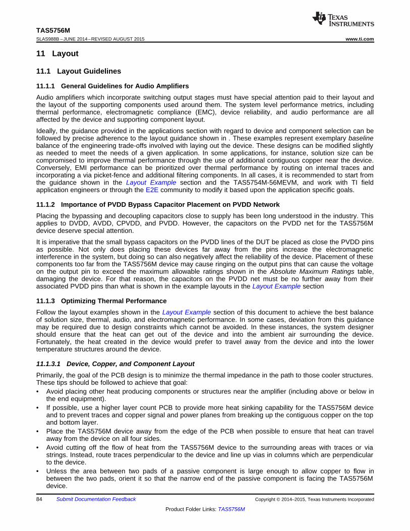
TAS5756MSLAS988B –JUNE 2014–REVISED AUGUST 2015 www.ti.com
11 Layout
11.1 Layout Guidelines
11.1.1 General Guidelines for Audio AmplifiersAudio amplifiers which incorporate switching output stages must have special attention paid to their layout andthe layout of the supporting components used around them. The system level performance metrics, includingthermal performance, electromagnetic compliance (EMC), device reliability, and audio performance are allaffected by the device and supporting component layout.
Ideally, the guidance provided in the applications section with regard to device and component selection can befollowed by precise adherence to the layout guidance shown in . These examples represent exemplary baselinebalance of the engineering trade-offs involved with laying out the device. These designs can be modified slightlyas needed to meet the needs of a given application. In some applications, for instance, solution size can becompromised to improve thermal performance through the use of additional contiguous copper near the device.Conversely, EMI performance can be prioritized over thermal performance by routing on internal traces andincorporating a via picket-fence and additional filtering components. In all cases, it is recommended to start fromthe guidance shown in the Layout Example section and the TAS5754M-56MEVM, and work with TI fieldapplication engineers or through the E2E community to modify it based upon the application specific goals.
11.1.2 Importance of PVDD Bypass Capacitor Placement on PVDD NetworkPlacing the bypassing and decoupling capacitors close to supply has been long understood in the industry. Thisapplies to DVDD, AVDD, CPVDD, and PVDD. However, the capacitors on the PVDD net for the TAS5756Mdevice deserve special attention.
It is imperative that the small bypass capacitors on the PVDD lines of the DUT be placed as close the PVDD pinsas possible. Not only does placing these devices far away from the pins increase the electromagneticinterference in the system, but doing so can also negatively affect the reliability of the device. Placement of thesecomponents too far from the TAS5756M device may cause ringing on the output pins that can cause the voltageon the output pin to exceed the maximum allowable ratings shown in the Absolute Maximum Ratings table,damaging the device. For that reason, the capacitors on the PVDD net must be no further away from theirassociated PVDD pins than what is shown in the example layouts in the Layout Example section
11.1.3 Optimizing Thermal PerformanceFollow the layout examples shown in the Layout Example section of this document to achieve the best balanceof solution size, thermal, audio, and electromagnetic performance. In some cases, deviation from this guidancemay be required due to design constraints which cannot be avoided. In these instances, the system designershould ensure that the heat can get out of the device and into the ambient air surrounding the device.Fortunately, the heat created in the device would prefer to travel away from the device and into the lowertemperature structures around the device.
11.1.3.1 Device, Copper, and Component LayoutPrimarily, the goal of the PCB design is to minimize the thermal impedance in the path to those cooler structures.These tips should be followed to achieve that goal:• Avoid placing other heat producing components or structures near the amplifier (including above or below in
the end equipment).• If possible, use a higher layer count PCB to provide more heat sinking capability for the TAS5756M device
and to prevent traces and copper signal and power planes from breaking up the contiguous copper on the topand bottom layer.
• Place the TAS5756M device away from the edge of the PCB when possible to ensure that heat can travelaway from the device on all four sides.
• Avoid cutting off the flow of heat from the TAS5756M device to the surrounding areas with traces or viastrings. Instead, route traces perpendicular to the device and line up vias in columns which are perpendicularto the device.
• Unless the area between two pads of a passive component is large enough to allow copper to flow inbetween the two pads, orient it so that the narrow end of the passive component is facing the TAS5756Mdevice.
84 Submit Documentation Feedback Copyright © 2014–2015, Texas Instruments Incorporated
Product Folder Links: TAS5756M

TAS5756Mwww.ti.com SLAS988B –JUNE 2014–REVISED AUGUST 2015
Layout Guidelines (continued)• Because the ground pins are the best conductors of heat in the package, maintain a contiguous ground plane
from the ground pins to the PCB area surrounding the device for as many of the ground pins as possible.
11.1.3.2 Stencil PatternThe recommended drawings for the TAS5756M device PCB foot print and associated stencil pattern are shownat the end of this document in the package addendum. Additionally, baseline recommendations for the viaarrangement under and around the device are given as a starting point for the PCB design. This guidance isprovided to suit the majority of manufacturing capabilities in the industry and prioritizes manufacturability over allother performance criteria. In elevated ambient temperatures or under high-power dissipation use-cases, thisguidance may be too conservative and advanced PCB design techniques may be used to improve thermalperformance of the system. It is important to note that the customer must verify that deviation from the guidanceshown in the package addendum, including the deviation explained in this section, meets the customer’s quality,reliability, and manufacturability goals.
11.1.3.2.1 PCB footprint and Via Arrangement
The PCB footprint (also known as a symbol or land pattern) communicates to the PCB fabrication vendor theshape and position of the copper patterns to which the TAS5756M device will be soldered. This footprint can befollowed directly from the guidance in the package addendum at the end of this data sheet. It is important tomake sure that the thermal pad, which connects electrically and thermally to the PowerPAD of the TAS5756Mdevice, be made no smaller than what is specified in the package addendum. This ensures that the TAS5756Mdevice has the largest interface possible to move heat from the device to the board.
The via pattern shown in the package addendum provides an improved interface to carry the heat from thedevice through to the layers of the PCB, because small diameter plated vias (with minimally-sized annular rings)present a low thermal-impedance path from the device into the PCB. Once into the PCB, the heat travels awayfrom the device and into the surrounding structures and air. By increasing the number of vias, as shown in theLayout Example section, this interface can benefit from improved thermal performance.
NOTEVias can obstruct heat flow if they are not constructed properly.
• Remove thermal reliefs on thermal vias, because they impede the flow of heat through the via.• Vias filled with thermally conductive material are best, but a simple plated via can be used to avoid the
additional cost of filled vias.• The drill diameter of 8 mils or less. Also, the distance between the via barrel and the surrounding planes
should be minimized to help heat flow from the via into the surrounding copper material. In all cases,minimum spacing should be determined by the voltages present on the planes surrounding the via andminimized wherever possible.
• Vias should be arranged in columns, which extend in a line radially from the heat source to the surroundingarea. This arrangement is shown in the Layout Example section.
• Ensure that vias do not cut-off power current flow from the power supply through the planes on internallayers. If needed, remove some vias which are farthest from the TAS5756M device to open up the currentpath to and from the device.
11.1.3.2.1.1 Solder Stencil
During the PCB assembly process, a piece of metal called a stencil on top of the PCB and deposits solder pasteon the PCB wherever there is an opening (called an aperture) in the stencil. The stencil determines the quantityand the location of solder paste that is applied to the PCB in the electronic manufacturing process. In mostcases, the aperture for each of the component pads is almost the same size as the pad itself.
However, the thermal pad on the PCB is quite large and depositing a large, single deposition of solder pastewould lead to manufacturing issues. Instead, the solder is applied to the board in multiple apertures, to allow thesolder paste to outgas during the assembly process and reduce the risk of solder bridging under the device. Thisstructure is called an aperture array, and is shown in the Layout Example section. It is important that the totalarea of the aperture array (the area of all of the small apertures combined) covers between 70% and 80% of thearea of the thermal pad itself.
Copyright © 2014–2015, Texas Instruments Incorporated Submit Documentation Feedback 85
Product Folder Links: TAS5756M

TAS5756MSLAS988B –JUNE 2014–REVISED AUGUST 2015 www.ti.com
11.2 Layout Example
11.2.1 2.0 (Stereo BTL) System
Figure 85. 2.0 (Stereo BTL) 3-D View
86 Submit Documentation Feedback Copyright © 2014–2015, Texas Instruments Incorporated
Product Folder Links: TAS5756M

TAS5756Mwww.ti.com SLAS988B –JUNE 2014–REVISED AUGUST 2015
Layout Example (continued)
Figure 86. 2.0 (Stereo BTL) Top Copper View
Copyright © 2014–2015, Texas Instruments Incorporated Submit Documentation Feedback 87
Product Folder Links: TAS5756M

TAS5756MSLAS988B –JUNE 2014–REVISED AUGUST 2015 www.ti.com
Layout Example (continued)11.2.2 Mono (PBTL) System
Figure 87. Mono (PBTL) 3-D View
88 Submit Documentation Feedback Copyright © 2014–2015, Texas Instruments Incorporated
Product Folder Links: TAS5756M

TAS5756Mwww.ti.com SLAS988B –JUNE 2014–REVISED AUGUST 2015
Layout Example (continued)
Figure 88. Mono (PBTL) Top Copper View
Copyright © 2014–2015, Texas Instruments Incorporated Submit Documentation Feedback 89
Product Folder Links: TAS5756M

TAS5756MSLAS988B –JUNE 2014–REVISED AUGUST 2015 www.ti.com
Layout Example (continued)11.2.3 2.1 (Stereo BTL + Mono PBTL) Systems
Figure 89. 2.1 (Stereo BTL + Mono PBTL) 3-D View
90 Submit Documentation Feedback Copyright © 2014–2015, Texas Instruments Incorporated
Product Folder Links: TAS5756M

TAS5756Mwww.ti.com SLAS988B –JUNE 2014–REVISED AUGUST 2015
Layout Example (continued)
Figure 90. 2.1 (Stereo BTL + Mono PBTL) Top Copper View
Copyright © 2014–2015, Texas Instruments Incorporated Submit Documentation Feedback 91
Product Folder Links: TAS5756M

TAS5756MSLAS988B –JUNE 2014–REVISED AUGUST 2015 www.ti.com
Layout Example (continued)11.2.4 2.2 (Dual Stereo BTL) Systems
Figure 91. 2.2 (Dual Stereo BTL) 3-D View
92 Submit Documentation Feedback Copyright © 2014–2015, Texas Instruments Incorporated
Product Folder Links: TAS5756M

TAS5756Mwww.ti.com SLAS988B –JUNE 2014–REVISED AUGUST 2015
Layout Example (continued)
Figure 92. 2.2 (Dual Stereo BTL) Top Copper View
Copyright © 2014–2015, Texas Instruments Incorporated Submit Documentation Feedback 93
Product Folder Links: TAS5756M

TAS5756MSLAS988B –JUNE 2014–REVISED AUGUST 2015 www.ti.com
Layout Example (continued)11.2.5 1.1 (Bi-Amped BTL) Systems
Figure 93. 1.1 (Bi-Amped BTL) 3-D View
94 Submit Documentation Feedback Copyright © 2014–2015, Texas Instruments Incorporated
Product Folder Links: TAS5756M

TAS5756Mwww.ti.com SLAS988B –JUNE 2014–REVISED AUGUST 2015
Layout Example (continued)
Figure 94. 2. 1.1 (Bi-Amped BTL) Top Copper View
Copyright © 2014–2015, Texas Instruments Incorporated Submit Documentation Feedback 95
Product Folder Links: TAS5756M

TAS5756MSLAS988B –JUNE 2014–REVISED AUGUST 2015 www.ti.com
12 Device and Documentation Support
12.1 Device Support
12.1.1 Device NomenclatureThe glossary listed in the Glossary section is a general glossary with commonly used acronyms and words whichare defined in accordance with a broad TI initiative to comply with industry standards such as JEDEC, IPC, IEEE,and others. The glossary provided in this section defines words, phrases, and acronyms that are unique to thisproduct and documentation, collateral, or support tools and software used with this product. For any additionalquestions regarding definitions and terminology, please see the e2e Audio Amplfier Forum.
Bridge tied load (BTL) is an output configuration in which one terminal of the speaker is connected to one half-bridge and the other terminal is connected to another half-bridge.
DUT refers to a device under test to differentiate one device from another.
Closed-loop architecture describes a topology in which the amplifier monitors the output terminals, comparingthe output signal to the input signal and attempts to correct for non-linearities in the output.
Dynamic controls are those which are changed during normal use by either the system or the end-user.
GPIO is a general purpose input/output pin. It is a highly configurable, bi-directional digital pin which can performmany functions as required by the system.
Host processor (also known as System Processor, Scalar, Host, or System Controller) refers to devicewhich serves as a central system controller, providing control information to devices connected to it as well asgathering audio source data from devices upstream from it and distributing it to other devices. This device oftenconfigures the controls of the audio processing devices (like the TAS5756M) in the audio path in order tooptimize the audio output of a loudspeaker based on frequency response, time alignment, target sound pressurelevel, safe operating area of the system, and user preference.
HybridFlow uses components which are built in RAM and components which are built in ROM to make aconfigurable device that is easier to use than a fully-programmable device while remaining flexible enough to beused in several applications
Maximum continuous output power refers to the maximum output power that the amplifier can continuouslydeliver without shutting down when operated in a 25°C ambient temperature. Testing is performed for the periodof time required that their temperatures reach thermal equilibrium and are no longer increasing
Parallel bridge tied load (PBTL) is an output configuration in which one terminal of the speaker is connected totwo half-bridges which have been placed in parallel and the other terminal is connected to another pair of halfbridges placed in parallel
rDS(on) is a measure of the on-resistance of the MOSFETs used in the output stage of the amplifier.
Static controls/Static configurations are controls which do not change while the system is in normal use.
Vias are copper-plated through-hole in a PCB.
12.1.2 Development SupportFor the PurePath Console Software, go to www.ti.com/tool/purepathconsole.
See the User Guide, Using the TAS5754/6M HybridFlow Processor (SLAU577) for detailed information regardingthe HybridFlow Processing and available HybridFlows.
12.2 Community ResourcesThe following links connect to TI community resources. Linked contents are provided "AS IS" by the respectivecontributors. They do not constitute TI specifications and do not necessarily reflect TI's views; see TI's Terms ofUse.
TI E2E™ Online Community TI's Engineer-to-Engineer (E2E) Community. Created to foster collaborationamong engineers. At e2e.ti.com, you can ask questions, share knowledge, explore ideas and helpsolve problems with fellow engineers.
96 Submit Documentation Feedback Copyright © 2014–2015, Texas Instruments Incorporated
Product Folder Links: TAS5756M
TAS5756Mwww.ti.com SLAS988B –JUNE 2014–REVISED AUGUST 2015
Community Resources (continued)Design Support TI's Design Support Quickly find helpful E2E forums along with design support tools and
contact information for technical support.
12.3 TrademarksPurePath, PowerPAD, E2E are trademarks of Texas Instruments.Burr-Brown is a registered trademark of Texas Instruments.All other trademarks are the property of their respective owners.
12.4 Electrostatic Discharge CautionThese devices have limited built-in ESD protection. The leads should be shorted together or the device placed in conductive foamduring storage or handling to prevent electrostatic damage to the MOS gates.
12.5 GlossarySLYZ022 — TI Glossary.
This glossary lists and explains terms, acronyms, and definitions.
13 Mechanical, Packaging, and Orderable InformationThe following pages include mechanical, packaging, and orderable information. This information is the mostcurrent data available for the designated devices. This data is subject to change without notice and revision ofthis document. For browser-based versions of this data sheet, refer to the left-hand navigation.
Copyright © 2014–2015, Texas Instruments Incorporated Submit Documentation Feedback 97
Product Folder Links: TAS5756M

PACKAGE OPTION ADDENDUM
www.ti.com 7-Aug-2015
Addendum-Page 1
PACKAGING INFORMATION
Orderable Device Status(1)
Package Type PackageDrawing
Pins PackageQty
Eco Plan(2)
Lead/Ball Finish(6)
MSL Peak Temp(3)
Op Temp (°C) Device Marking(4/5)
Samples
TAS5756MDCA ACTIVE HTSSOP DCA 48 40 Green (RoHS& no Sb/Br)
CU NIPDAU Level-3-260C-168 HR -25 to 85 TAS5756M
TAS5756MDCAR ACTIVE HTSSOP DCA 48 2000 Green (RoHS& no Sb/Br)
CU NIPDAU Level-3-260C-168 HR -25 to 85 TAS5756M
(1) The marketing status values are defined as follows:ACTIVE: Product device recommended for new designs.LIFEBUY: TI has announced that the device will be discontinued, and a lifetime-buy period is in effect.NRND: Not recommended for new designs. Device is in production to support existing customers, but TI does not recommend using this part in a new design.PREVIEW: Device has been announced but is not in production. Samples may or may not be available.OBSOLETE: TI has discontinued the production of the device.
(2) Eco Plan - The planned eco-friendly classification: Pb-Free (RoHS), Pb-Free (RoHS Exempt), or Green (RoHS & no Sb/Br) - please check http://www.ti.com/productcontent for the latest availabilityinformation and additional product content details.TBD: The Pb-Free/Green conversion plan has not been defined.Pb-Free (RoHS): TI's terms "Lead-Free" or "Pb-Free" mean semiconductor products that are compatible with the current RoHS requirements for all 6 substances, including the requirement thatlead not exceed 0.1% by weight in homogeneous materials. Where designed to be soldered at high temperatures, TI Pb-Free products are suitable for use in specified lead-free processes.Pb-Free (RoHS Exempt): This component has a RoHS exemption for either 1) lead-based flip-chip solder bumps used between the die and package, or 2) lead-based die adhesive used betweenthe die and leadframe. The component is otherwise considered Pb-Free (RoHS compatible) as defined above.Green (RoHS & no Sb/Br): TI defines "Green" to mean Pb-Free (RoHS compatible), and free of Bromine (Br) and Antimony (Sb) based flame retardants (Br or Sb do not exceed 0.1% by weightin homogeneous material)
(3) MSL, Peak Temp. - The Moisture Sensitivity Level rating according to the JEDEC industry standard classifications, and peak solder temperature.
(4) There may be additional marking, which relates to the logo, the lot trace code information, or the environmental category on the device.
(5) Multiple Device Markings will be inside parentheses. Only one Device Marking contained in parentheses and separated by a "~" will appear on a device. If a line is indented then it is a continuationof the previous line and the two combined represent the entire Device Marking for that device.
(6) Lead/Ball Finish - Orderable Devices may have multiple material finish options. Finish options are separated by a vertical ruled line. Lead/Ball Finish values may wrap to two lines if the finishvalue exceeds the maximum column width.
Important Information and Disclaimer:The information provided on this page represents TI's knowledge and belief as of the date that it is provided. TI bases its knowledge and belief on informationprovided by third parties, and makes no representation or warranty as to the accuracy of such information. Efforts are underway to better integrate information from third parties. TI has taken andcontinues to take reasonable steps to provide representative and accurate information but may not have conducted destructive testing or chemical analysis on incoming materials and chemicals.TI and TI suppliers consider certain information to be proprietary, and thus CAS numbers and other limited information may not be available for release.

PACKAGE OPTION ADDENDUM
www.ti.com 7-Aug-2015
Addendum-Page 2
In no event shall TI's liability arising out of such information exceed the total purchase price of the TI part(s) at issue in this document sold by TI to Customer on an annual basis.

TAPE AND REEL INFORMATION
*All dimensions are nominal
Device PackageType
PackageDrawing
Pins SPQ ReelDiameter
(mm)
ReelWidth
W1 (mm)
A0(mm)
B0(mm)
K0(mm)
P1(mm)
W(mm)
Pin1Quadrant
TAS5756MDCAR HTSSOP DCA 48 2000 330.0 24.4 8.6 13.0 1.8 12.0 24.0 Q1
PACKAGE MATERIALS INFORMATION
www.ti.com 14-Dec-2017
Pack Materials-Page 1

*All dimensions are nominal
Device Package Type Package Drawing Pins SPQ Length (mm) Width (mm) Height (mm)
TAS5756MDCAR HTSSOP DCA 48 2000 367.0 367.0 45.0
PACKAGE MATERIALS INFORMATION
www.ti.com 14-Dec-2017
Pack Materials-Page 2

IMPORTANT NOTICE
Texas Instruments Incorporated (TI) reserves the right to make corrections, enhancements, improvements and other changes to itssemiconductor products and services per JESD46, latest issue, and to discontinue any product or service per JESD48, latest issue. Buyersshould obtain the latest relevant information before placing orders and should verify that such information is current and complete.TI’s published terms of sale for semiconductor products (http://www.ti.com/sc/docs/stdterms.htm) apply to the sale of packaged integratedcircuit products that TI has qualified and released to market. Additional terms may apply to the use or sale of other types of TI products andservices.Reproduction of significant portions of TI information in TI data sheets is permissible only if reproduction is without alteration and isaccompanied by all associated warranties, conditions, limitations, and notices. TI is not responsible or liable for such reproduceddocumentation. Information of third parties may be subject to additional restrictions. Resale of TI products or services with statementsdifferent from or beyond the parameters stated by TI for that product or service voids all express and any implied warranties for theassociated TI product or service and is an unfair and deceptive business practice. TI is not responsible or liable for any such statements.Buyers and others who are developing systems that incorporate TI products (collectively, “Designers”) understand and agree that Designersremain responsible for using their independent analysis, evaluation and judgment in designing their applications and that Designers havefull and exclusive responsibility to assure the safety of Designers' applications and compliance of their applications (and of all TI productsused in or for Designers’ applications) with all applicable regulations, laws and other applicable requirements. Designer represents that, withrespect to their applications, Designer has all the necessary expertise to create and implement safeguards that (1) anticipate dangerousconsequences of failures, (2) monitor failures and their consequences, and (3) lessen the likelihood of failures that might cause harm andtake appropriate actions. Designer agrees that prior to using or distributing any applications that include TI products, Designer willthoroughly test such applications and the functionality of such TI products as used in such applications.TI’s provision of technical, application or other design advice, quality characterization, reliability data or other services or information,including, but not limited to, reference designs and materials relating to evaluation modules, (collectively, “TI Resources”) are intended toassist designers who are developing applications that incorporate TI products; by downloading, accessing or using TI Resources in anyway, Designer (individually or, if Designer is acting on behalf of a company, Designer’s company) agrees to use any particular TI Resourcesolely for this purpose and subject to the terms of this Notice.TI’s provision of TI Resources does not expand or otherwise alter TI’s applicable published warranties or warranty disclaimers for TIproducts, and no additional obligations or liabilities arise from TI providing such TI Resources. TI reserves the right to make corrections,enhancements, improvements and other changes to its TI Resources. TI has not conducted any testing other than that specificallydescribed in the published documentation for a particular TI Resource.Designer is authorized to use, copy and modify any individual TI Resource only in connection with the development of applications thatinclude the TI product(s) identified in such TI Resource. NO OTHER LICENSE, EXPRESS OR IMPLIED, BY ESTOPPEL OR OTHERWISETO ANY OTHER TI INTELLECTUAL PROPERTY RIGHT, AND NO LICENSE TO ANY TECHNOLOGY OR INTELLECTUAL PROPERTYRIGHT OF TI OR ANY THIRD PARTY IS GRANTED HEREIN, including but not limited to any patent right, copyright, mask work right, orother intellectual property right relating to any combination, machine, or process in which TI products or services are used. Informationregarding or referencing third-party products or services does not constitute a license to use such products or services, or a warranty orendorsement thereof. Use of TI Resources may require a license from a third party under the patents or other intellectual property of thethird party, or a license from TI under the patents or other intellectual property of TI.TI RESOURCES ARE PROVIDED “AS IS” AND WITH ALL FAULTS. TI DISCLAIMS ALL OTHER WARRANTIES ORREPRESENTATIONS, EXPRESS OR IMPLIED, REGARDING RESOURCES OR USE THEREOF, INCLUDING BUT NOT LIMITED TOACCURACY OR COMPLETENESS, TITLE, ANY EPIDEMIC FAILURE WARRANTY AND ANY IMPLIED WARRANTIES OFMERCHANTABILITY, FITNESS FOR A PARTICULAR PURPOSE, AND NON-INFRINGEMENT OF ANY THIRD PARTY INTELLECTUALPROPERTY RIGHTS. TI SHALL NOT BE LIABLE FOR AND SHALL NOT DEFEND OR INDEMNIFY DESIGNER AGAINST ANY CLAIM,INCLUDING BUT NOT LIMITED TO ANY INFRINGEMENT CLAIM THAT RELATES TO OR IS BASED ON ANY COMBINATION OFPRODUCTS EVEN IF DESCRIBED IN TI RESOURCES OR OTHERWISE. IN NO EVENT SHALL TI BE LIABLE FOR ANY ACTUAL,DIRECT, SPECIAL, COLLATERAL, INDIRECT, PUNITIVE, INCIDENTAL, CONSEQUENTIAL OR EXEMPLARY DAMAGES INCONNECTION WITH OR ARISING OUT OF TI RESOURCES OR USE THEREOF, AND REGARDLESS OF WHETHER TI HAS BEENADVISED OF THE POSSIBILITY OF SUCH DAMAGES.Unless TI has explicitly designated an individual product as meeting the requirements of a particular industry standard (e.g., ISO/TS 16949and ISO 26262), TI is not responsible for any failure to meet such industry standard requirements.Where TI specifically promotes products as facilitating functional safety or as compliant with industry functional safety standards, suchproducts are intended to help enable customers to design and create their own applications that meet applicable functional safety standardsand requirements. Using products in an application does not by itself establish any safety features in the application. Designers mustensure compliance with safety-related requirements and standards applicable to their applications. Designer may not use any TI products inlife-critical medical equipment unless authorized officers of the parties have executed a special contract specifically governing such use.Life-critical medical equipment is medical equipment where failure of such equipment would cause serious bodily injury or death (e.g., lifesupport, pacemakers, defibrillators, heart pumps, neurostimulators, and implantables). Such equipment includes, without limitation, allmedical devices identified by the U.S. Food and Drug Administration as Class III devices and equivalent classifications outside the U.S.TI may expressly designate certain products as completing a particular qualification (e.g., Q100, Military Grade, or Enhanced Product).Designers agree that it has the necessary expertise to select the product with the appropriate qualification designation for their applicationsand that proper product selection is at Designers’ own risk. Designers are solely responsible for compliance with all legal and regulatoryrequirements in connection with such selection.Designer will fully indemnify TI and its representatives against any damages, costs, losses, and/or liabilities arising out of Designer’s non-compliance with the terms and provisions of this Notice.
Mailing Address: Texas Instruments, Post Office Box 655303, Dallas, Texas 75265Copyright © 2017, Texas Instruments Incorporated