T2K TPC Read-out Electronics Digital Front-end Mezzanine ...
100
03/08/2007 T2K TPC Read-out Electronics Digital Front-end Mezzanine Card Design Notes Denis Calvet CEA Saclay, DSM/DAPNIA/SEDI I. Introduction 1. Scope This note describes the design of the digital front-end mezzanine card (FEM) for the read- out electronics of the TPCs at T2K 280 m. The hardware is detailed along with the interface to the analog front-end cards (FEC) and the off-detector back-end data concentrator cards (DCC). Firmware and software is described along with tests and measurements on the various prototype boards. 2. Brief outline of the TPC readout architecture The architecture for TPC readout has been described in the Conceptual Design Report (CDR). It consists of two main parts: on-detector electronics mounted at the back of the gas amplification modules inside the magnet, and off-detector electronics housed in standard racks at B2 floor. Each of the 2 end-plates of the 3 TPCs comprises a certain number of detector modules segmented in pads. The number of modules and the number of pads per module have been fluctuating parameters over time, following the evolution of the design of the detector and technology choices. The design of the electronics cannot wait for final decisions on these parameters and a modular design that can adapt quickly to various scenarios is crucial. The readout system of each detector module is made identical. It comprises a certain number of Front-End Cards (FECs), each equipped with 4 custom ASICs (called AFTER which stands for “Asic For Tpc Electronic Readout”). The FECs are driven by a Front-End Mezzanine (FEM) card. Each FEM card is linked to an off-detector Data Concentrator Card (DCC) via a duplex optical fiber. Since the CDR several decisions have been made as described and justified below. The FECs are mounted orthogonally to the plane of the detector for the following reasons: • the total PCB area of the FECs can be made larger than the size of the detector module (it is not guaranteed that all components would fit if read-out was made by only 1 FEC parallel to the plane of the detector module); • the FEC can be designed before the exact dimensions and segmentation of the detector module are fixed; • the architecture can accommodate detector segmentation changes by varying the number of FECs per read-out module. The FEM is mounted astride of the FECs. Consequently, the number of FECs per module must be known to build the final FEM. A key point is to have a parameterized design for the FEM, so that the largest parts of the design can be made without the final value of detector channel count. The detector module readout architecture shown in Fig. 1 is the latest version (and probably final): it comprises 6 FECs per FEM (compared to 4 as initially planned in the CDR). There are 72 detector modules in the complete system (instead of 84 as described in the CDR). In the text that follows, some sections have been written prior to these choices (i.e. at the time when the baseline design had 4 FECs per FEM), while others (like this introduction) have been written after. This explains that the emphasis is not always placed on the same option.
Transcript of T2K TPC Read-out Electronics Digital Front-end Mezzanine ...

03/08/2007
T2K TPC Read-out Electronics Digital Front-end Mezzanine Card Design Notes
Denis Calvet
CEA Saclay, DSM/DAPNIA/SEDI
I. Introduction 1. Scope
This note describes the design of the digital front-end mezzanine card (FEM) for the read-out electronics of the TPCs at T2K 280 m. The hardware is detailed along with the interface to the analog front-end cards (FEC) and the off-detector back-end data concentrator cards (DCC). Firmware and software is described along with tests and measurements on the various prototype boards.
2. Brief outline of the TPC readout architecture The architecture for TPC readout has been described in the Conceptual Design Report
(CDR). It consists of two main parts: on-detector electronics mounted at the back of the gas amplification modules inside the magnet, and off-detector electronics housed in standard racks at B2 floor. Each of the 2 end-plates of the 3 TPCs comprises a certain number of detector modules segmented in pads. The number of modules and the number of pads per module have been fluctuating parameters over time, following the evolution of the design of the detector and technology choices. The design of the electronics cannot wait for final decisions on these parameters and a modular design that can adapt quickly to various scenarios is crucial. The readout system of each detector module is made identical. It comprises a certain number of Front-End Cards (FECs), each equipped with 4 custom ASICs (called AFTER which stands for “Asic For Tpc Electronic Readout”). The FECs are driven by a Front-End Mezzanine (FEM) card. Each FEM card is linked to an off-detector Data Concentrator Card (DCC) via a duplex optical fiber. Since the CDR several decisions have been made as described and justified below. The FECs are mounted orthogonally to the plane of the detector for the following reasons:
• the total PCB area of the FECs can be made larger than the size of the detector module (it is not guaranteed that all components would fit if read-out was made by only 1 FEC parallel to the plane of the detector module);
• the FEC can be designed before the exact dimensions and segmentation of the detector module are fixed;
• the architecture can accommodate detector segmentation changes by varying the number of FECs per read-out module.
The FEM is mounted astride of the FECs. Consequently, the number of FECs per module must be known to build the final FEM. A key point is to have a parameterized design for the FEM, so that the largest parts of the design can be made without the final value of detector channel count. The detector module readout architecture shown in Fig. 1 is the latest version (and probably final): it comprises 6 FECs per FEM (compared to 4 as initially planned in the CDR). There are 72 detector modules in the complete system (instead of 84 as described in the CDR). In the text that follows, some sections have been written prior to these choices (i.e. at the time when the baseline design had 4 FECs per FEM), while others (like this introduction) have been written after. This explains that the emphasis is not always placed on the same option.

2
72-channel ASIC“AFTER”
Quad-channel ADC
Front-EndMezzanine
card
Optical transceiver
FPGA logic
80-pin connector
288-channel Front-End Card 1728-pad Micromegas module
Slow controlnetworkdaisy-chain
Duplex opticalfiber to DCC
Power bar
1 of 72 modules
Low voltageinput(4-5 V)
Fig. 1. Read-out module concept.
The complete architecture of the TPC read-out system is shown in Fig. 2.
1728 AFTER chipson 432 FECs
72 FEMs
124.416 input pads over 72 modules
6 DCCs
PC
On-detector (B1)
Off-detector (B2)
Gb Ethernetto DAQ
~25 m optical fibers
L.V. PowersuppliesPC
Slow control(shared)
3-6chains
Clock, Trigger
Fig. 2. TPC readout architecture.
II. Reduced FEM cards 1. Concept
Developing the full size FEM card directly is somewhat challenging and is not even possible until the final number of FECs per FEM is frozen. Some digital hardware that implements most of the functions of the FEM card is however needed to drive the test bench of the ASIC and also to drive the prototype of the FEC. There is no fundamental difference between the logic that drives a single ASIC on the testbench, a single FEC with 4 ASICs, or several FECs. The largest part of the corresponding firmware should be common to these different configurations. All developments and validation can be done on some existing FPGA board connected via an adaptation card to the test card of the ASIC or the prototype FEC. Because of I/O pin count limitations on commercial FPGA kits and for simplicity, only one ASIC test card or FEC can be driven. Hence, this makes a “reduced FEM card”. This

3
reduced FEM card allows building with minimal effort the digital part of the test bench of the ASIC and the test bench of the FEC. It also serves as an early prototype of the FEM where most of the concepts of the FEM can be implemented, tested and debugged before the full size FEM card is actually built.
2. Variations Two versions of the reduced FEM are being designed: one is based on the USB
configurable test probe “STUC”; the second one is based on a commercial evaluation kit from Avnet/Memec (Xilinx Virtex 2 Pro) [2]. The STUC version is aimed to the most efficient and direct acquisition of the data from the ASIC testbench or prototype FEC. It uses a USB 2 interface to attach directly to a data acquisition PC. This configuration shall be used to test the characteristics and the performance of the ASIC with optimal data acquisition speed. The control PC used runs Windows; data acquisition and analysis is made with LabView. This configuration is shown in Fig. 3.
Front-end ASIC Test
Card
Front-endCard
STUC
Agreed connector
ReducedFEM Stuc
Windows, Labview
USB
Front-end ASIC Test
Card
Front-endCard
STUC
Agreed connector
ReducedFEM Stuc
Windows, Labview
USB
Fig. 3. ASIC and Front-end card test bench for characterization.
The Virtex 2 Pro kit based version brings the additional capability to perform all the control and data acquisition through an optical Gigabit speed link similar to the one that is foreseen for the interface to the back-end Data Concentrator Card. A simplified DCC is fitted in the same hardware to drive an optical transceiver looped back to the optical transceiver of the reduced FEM card. The simplified DCC is connected via the on-board Fast Ethernet interface to a control PC. This configuration is used to develop and validate the interface between the FEM and the DCC in realistic conditions. It can also perform the control and data acquisition of 1 FEC. The control PC may run Linux or another operating system. This configuration is shown in Fig. 4.
Front-end ASIC Test
Card
Front-endCard
Optical fiber
ReducedFEM 2
Windows, LabviewLinux, others
FastEthernet
XC2VP
FEMDCC Kit Memec
Front-end ASIC Test
Card
Front-endCard
Optical fiber
ReducedFEM 2
Windows, LabviewLinux, others
FastEthernet
XC2VP
FEMDCC Kit Memec
Fig. 4. Development of the interface between the DCC and FEM.
In a later step, the simplified DCC and reduced FEM are fitted in 2 different evaluation kits. The simplified DCC may drive 2 objects simultaneously. Each object may be a reduced FEM card connected to a FEC or the full prototype FEM connected to one or several FECs. This is shown in Fig. 5.

4
Optical fibers
ReducedFEM 2
XC2VP
FEMWindows, Labview
Linux, others
FastEthernet
XC2VP
DCC Kit Memec
Reduced FEMOr
Prototype FEMOptical fibers
ReducedFEM 2
XC2VP
FEMWindows, Labview
Linux, others
FastEthernet
XC2VP
DCC Kit Memec
Reduced FEMOr
Prototype FEM
Fig. 5. Driving multiple FEMs with a reduced DCC.
These configurations of growing complexity allow the progressive development of more complex systems that are getting closer and closer to the final system. In the largest configuration where the DCC is the commercial kit being used, a system capable of controlling 2 fully equipped detector modules, each with 1 FEM card and 4 (or 6) FECs can be devised. This major milestone for the project must be reached before any of the final cards is produced.
3. Development plan The 2 versions of the reduced FEM cards can be developed in parallel with minimal
additional effort: they include the same components, only the interface connector to the FPGA logic and the mechanical format is different. The interface connector between the ASIC test bench card and the FEC must be defined and agreed. The largest part of the specific logic and components that are foreseen on the final FEM should be placed on these reduced FEM cards for test, firmware and software development, and validation.
III. FEM card on-board components This section describes the full-size FEM card. The main components of the card are: • a large FPGA device that implements most of the logic functions of the card, • an in-situ programmable JTAG Flash memory for storing FPGA configuration
bitstream, • a buffer memory for storing data digitized by the FECs until they can be sent to the
DCCs, • an optical transceiver for communicating with the DCCs, • a local oscillator for clocking the FPGA, • glue logic to fanout some of the signals produced by the FPGA to the FECs, and
multiplex signals from the FECs before driving the inputs of the FPGA, • one interface connector per FEC, • a hardwired silicon ID number to uniquely identify each FEM card, • means for monitoring various voltages, currents and temperatures, • a micro-controller dedicated to the slow control and monitoring of the FEM and FECs, • a connector for the slow control network cable, • debug outputs/inputs for a logic analyzer/oscilloscope; these also serves as an
expansion slot for unanticipated hardware add-on, • voltage regulators for all on-board components,

5
• a connector for bringing external power to the FEM card, • de-coupling circuits for all devices, • a power-on RESET circuit, • visual LED indicators for comfort when debugging, • test points.
1. FPGA target
1.1. Vendor and family Several FPGA targets have been considered, all from Xilinx because of personal
experience and knowledge. Another advantage of Xilinx compared to its competitor is the availability of low priced evaluation kits that allow fast prototyping – especially of high speed optical links. Among Xilinx parts, all devices older than the Virtex 2 are clearly not recommended for new designs. An important feature of the FEM is the need for a fast (optical) communication link. Some FPGA families do not include embedded transceivers. An external device would be needed in this case. This extra device would consume more power than a transceiver integrated in a FPGA, increases cost and complexity, and is less flexible. Therefore FPGA devices with embedded transceivers have been favored. The Virtex 2 Pro family is ideally suited: the device is mature and a large choice of gate densities and packages are available.
The newer Virtex 4 family is at present the most advanced, but unfortunately only large devices in the Virtex 4 FX family incorporate gigabit transceivers. The smallest part in the family, the XC4VFX12 has an embedded PowerPC 405 processor, but no RocketIO transceiver. The next device in the family, the XC4VFX20 has 8 RocketIO transceivers. This is much more than what is needed for the FEM. For marketing reasons presumably, there is no device in the Virtex 4 family equivalent to low-end Virtex 2 Pros (i.e. 4 RocketIO and no or one PowerPC core). When the design of the FEM started, none of the Virtex 4 devices with RocketIO transceivers was available. The parts are now available since ~Q2 2006, but the evaluation kits will probably not come until Q3-Q4 2006. For this reason, it has been decided to use a device from the Virtex 2 Pro family rather than the Virtex 4 family. The last argument is economical. At present, the XC4VFX20 is much more expensive than the XC2VP4 (~259 $ for a XC4VFX20-10FF672C versus 163 $ for a XC2VP4 in the same package), and although the price of Virtex 4 devices decreases, it is possible that the price difference remains significant.
1.2. Part number, package and speed grade The latest estimate indicates that for a FEM driving 4 FEC, the XC2VP2 (i.e. the smallest
part in the Virtex 2 Pro family) is not sufficient in terms of logic resources. The XC2VP4 is therefore required. For a 6 FEC scheme, the XC2VP4 is comfortably sufficient in terms of logic resources. The XC2VP4 has 4 RocketIO transceivers (3.125 Gbps maximum), an embedded PowerPC 405 processor (32 bit RISC clocked at up to 300 MHz with 16 KB + 16 KB caches).
At present, it is not foreseen to use an embedded processor on the FEM, and all functions are thought to be coded in programmable logic. If design time allows, the PowerPC embedded in the FPGA target could be used to perform zero-suppression for example. However, it is not foreseen to have an external program / data memory for that processor, and one would have to rely on embedded memory blocks. The XC2VP4 has 28 memory blocks of 18 Kbit. One block is needed in the interface to the ADC of each FEC, and a few other blocks are used, leaving at least 16 blocks available. If the necessary additional logic is available, the 16 memory blocks could be used by the embedded processor to make 16 KB of program memory

6
and 16 KB of data memory. The program run by the embedded processor would have to fit in this space. Because all memory would be inside the FPGA, the program can be inserted in the FPGA configuration bitstream. It is conceivable to download some executable code via the optical link; but this requires additional resources and more development time.
Two packages can be considered depending on the required number of user I/O pins. The FG456 package has 248 available I/O pins while the FF672 package has 348 available I/Os. Note that these numbers include the I/O pins used for device configuration (serial or parallel PROM) and also include the special reference voltage pins used in certain I/O signaling standards. Care must be taken also to the fact that voltage mixing within an I/O bank is not possible, and the number of simultaneous switching outputs per bank is limited. The current estimate for user I/O pin count is 170 and 227 for the 4 and 6 FEC schemes respectively. Clearly, the FG456 package is not adequate for the 6 FEC scheme. The cost difference between the 2 packages is however rather small (~10€), and the FF672 package may be chosen. At present, a -5 speed grade seems sufficient to reach the target speed.
The current proposed part number is: XC2VP4-5FFG672C (128 $ per 100 on Avnet web site in June 2006). The “G” suffix (Green) indicates that the part is RoHS compliant.
2. FPGA configuration
2.1. Principle The FEM cards should be operational shortly after power up. It is much more practical to
store the FPGA firmware locally rather than download a binary file from the outside of the magnet after each power cut. Nonetheless, it must be possible to upgrade the firmware of all FEMs without opening the magnet. Because decision is made not to use any external memory for the eventual software that may run on the embedded PowerPC processor of the FEM FPGA, a low cost in-situ programmable JTAG PROM from Xilinx is sufficient. A flash memory (eventually removable) brings more flexibility but is more complex (a small CPLD is generally needed to interface to the FPGA) and more expensive. During development and debugging, it is useful to be able to configure the FPGA directly via JTAG, and burn into the configuration PROM only a stabilized version of the bitstream. The content of the PROM shall be modifiable by attaching a JTAG cable directly to the card, or remotely via a slow control path accessible from the outside of the TPC.
2.2. Configuration PROM and protocol The bitstream of a XC2VP4 device is ~3 Mbit. Two Xilinx PROM devices are adequate:
the XCF04S (4 Mbit) or the XCF08S (8 Mbit). The XCF08S brings the advantage of design revisioning, but requires a 1.8V supply voltage that no other device on the card is likely to need. It is therefore proposed to use the least sophisticated option based on a XCF04S. This device can operate from 3.3V only, or 2.5V can be used for the I/Os (but the core always needs 3.3V).
There is no strict constraint on the wake-up time of the FEM after power-up (e.g. 1 s is fine), and the configuration scheme that minimizes the number of FPGA I/O pins and PCB traces is chosen, i.e. the Master Serial configuration mode. Assuming a configuration clock of 10 MHz, the configuration time is ~0.3 s. The adequate PROM part number is XCF04S-VOG20C. This part is RoHS compliant. Alternatively, a XCF04S-VOG48C could be used (this part supports also the parallel configuration mode). The FPGA shall support JTAG configuration mode for development. By default, the FPGA shall be set for configuration in Master Serial mode. Through jumpers, it can be set to JTAG configuration mode. Other configuration modes are not supported.

7
2.3. JTAG chains Two JTAG chains are present on the FEM board. One chain contains only the micro-
controller used for the slow control network. The corresponding connector header is used to program in-situ the on-chip flash memory of the micro-controller. The second JTAG chain consists of 2 devices: the FPGA and its configuration PROM. This JTAG chain can be driven by 2 different means: a connector header on the FEM, or a JTAG port emulated in software by the micro-controller attached to the slow control network. The connector header receives a Xilinx JTAG cable during the development and test phase of the FPGA firmware; the JTAG port emulated over the slow control network is used to upgrade FPGA firmware in-situ, i.e. when the FEM card cannot be accessed. A jumper is used to select whether the FPGA and PROM JTAG chain signals are taken from the connector header or from micro-controller I/O ports. The I/O ports of the micro-controller are 3.3V only while the JTAG pins of the serial PROM are either 3.3V or 2.5V (depending on VCCJ) and the JTAG pins of the FPGA are powered with 2.5V (VCCAUX) but are 3.3V tolerant [3]. Because powering these pins from 3.3V requires some extra precautions [4], it is preferable to use the recommended 2.5V levels and make 3.3V to 2.5V translation on the micro-controller pins that drive JTAG output signals O_TCK, O_TMS and O_TDI. This is accomplished by the multiplexer. The 2 JTAG chains are shown in Fig. 6.
MUX2:1
JTAG headerFPGA/PROM
µC
TCK
JTAG headerMicro-controller
PROM
FPGA
TDI
TMS
TDO
TDI TDO
TCK
TMSO_TMS
O_TCK
O_TDI
I_TDO
TCKTMSTDI
TCK
TMS
TDI TDO
TDO
VCCAUX 2.5V FPGA
SELVDD = 3.3V uCR>200
3.3V FPGA
VCCJ = 2.5V FPGAVCCINT = 3.3V FPGA
VCCAUX = 2.5V FPGA
VCCINT = 1.5VVCCAUX = 2.5V FPGAVCCO_4 = 2.5V FPGAVCCO_5 = 2.5V FPGA
JP0V
VCC =2.5V FPGA
R
3.3VFPGA
Pullup to 2.5VTerm. TCK: 100 pF + 50 ohms to 0V_FPGA
4.7k
Mux
3.3V uC
Fig. 6. JTAG Chains.
For the JTAG header dedicated to the micro-controller, no external pullup resistor is needed on any pin because these are integrated in the micro-controller chip (but a recommended termination circuit is placed on TCK). On the general purpose I/O pins that emulate JTAG for the FPGA chain, pullup resistors are needed to prevent O_TCK, O_TMS and O_TDI from floating when the micro-controller I/O pins are not configured or tri-stated. When jumper JP is installed, JTAG signals for the FPGA chain are taken from the header. It is expected that a Xilinx cable is present, and therefore the signals at the input of the multiplexer are not left floating. However, if the jumper is installed, but no Xilinx programming cable is plugged-in, pullup resistors are needed to keep the inputs of the multiplexer in the known inactive state (i.e. a high level for TMS and TDI) and a termination circuit (50 ohms in series with 100 pF) is placed on TCK. The multiplexer does not have tri-state capability: on its output side, TCK, TMS (and TDI on the PROM) are always driven. No pullup resistor is needed on the TDI pin of the FPGA because the PROM has an internal pullup to VCCJ on pin TDO. The TDO pin of the FPGA is an open drain output, and a pullup resistor must be placed. This pin is powered by VCCAUX=2.5V but can be pulled up to 3.3V with a recommended resistor greater than 200 ohms. Note that because this pin is open drain, it does not sink reverse current as explained in [4]. Being pulled up to 3.3V levels, the TDO

8
pin of the FPGA can interface directly to the micro-controller input I_TDO. However, 3.3V to 2.5V translation is needed to interface to the JTAG Xilinx cable. A dual-input multiplexer configured as a single-input non-inverting gate is used (the 3 other multiplexers available in the package are used to select the source of TMS, TCK and TDI). Note that choosing VCCAUX=2.5V on the PROM side imposes that 2.5V I/Os are used on banks 4 and 5 of the FPGA. The micro-controller should not drive the emulated JTAG port before the FPGA logic is powered. This should be guaranteed by software.
The recommended part number for the multiplexer is 74LCX157M (Fairchild Semiconductor). This part is RoHS compliant. This device has 5V tolerant inputs that do not include clamping diodes to the VCC pin. No current can therefore be injected through the input pins to the power supply pin if some inputs are driven when the power supply is not present (but this situation is not recommended anyway). The connector receiving the Xilinx cable is a 2x7 pin 2 mm pitch male header, part number MOLEX 87831-1420 (straight pin through hole, RoHS compliant). Alternate parts are MOLEX 87832-1420 (surface mount, RoHS compliant) or MOLEX 87833-1420 (pin through hole, right angled, RoHS compliant). The JTAG connector for programming the micro-controller is a 2x5 pin 2.54 mm pitch HE10, shrouded male header, preferably straight. The pinout is specified in the documentation of the micro-controller evaluation board.
3. Front-end card ADC The maximum retention time of the analog signals in the SCAs is ~2.5 ms. All front end
ASICs must be completely read-out before this volatile information is degraded. Assuming a maximum drift time of ~500 µs for the slowest gas being considered, the time budget that is left for digitization is ~2 ms. To read-out one time bucket in all channels of an ASIC, 79 analog values are converted. Hence to read-out a complete ASIC, 512*79=40448 conversions are made in ~2 ms. The minimum conversion rate for the ADC is therefore ~20 MHz. The required precision is 10-bit. Using commonly found parallel output ADCs would lead to a large number of I/O pins (~180-260) for the interface with the FPGA of the mezzanine card. This would need specific attention given the anticipated length of the connection (up to ~15 cm) and could generate excessive switching noise close to sensitive analog circuits. To solve some of the potential issues of traditional ADCs, devices integrating multiple ADCs on a single chip with high speed serial LVDS outputs have been selected. Two candidate devices have been investigated: Analog Devices AD 9229 and Texas Instruments ADS 5240. Both devices are 12-bit resolution quad-channel ADCs and operate from a single 3.3V power supply. Evaluation kits for both devices have been purchased and tested. The Texas part offers more flexibility in test patterns and serialization format. The Analog Devices part has however the decisive advantage of fast re-locking when the sampling clock is suppressed then re-applied. Measurements show that after applying the clock, the AD 9229 and de-serializer logic becomes operational after no more than ~40 µs (over 32.000 trials) while we could not have the ADS 5240 re-lock reliably even after several tens of milliseconds. The AD 9229 has also a wider range of sampling rate (from 10 MHz to 50/65 MHz) while the ADS 5240 cannot operate below 20 MHz. Given the previous considerations, the selected part is AD9229BCPZ-50. This part is lead-free.
4. Buffer Memory
4.1. Speed and size requirement The digital information produced per ASIC for each event is 512*79*12 = 474 Kbit. For a
mezzanine reading 4 (6) FEC, the raw event size is therefore 7584 Kbit (11.376 Kbit). The access speed for writing into the memory has to match the output rate of the ADCs. Assuming a 20 MHz ADC sampling rate, the required bandwidth for a 4 (6) FEC FEM is: 16*20E6*12
9
= 3.84 Gbit/s (5.76 Gbit/s). The required size is too large to be found in a FPGA device, and the required bandwidth can only be satisfied by using a synchronous memory. Each ADC (when clocked at 20 MHz) produces a data stream at 120 MHz per pin using DDR. The external interface to 4 (6) quad-ADC devices is a 16-bit (24-bit) wide bus, clocked at 120 MHz DDR (i.e. 240 Mbit/s per pin). In addition, each ADC produces a framing pattern which is equivalent to an ADC channel sending a constant value (“111111000000”). Hence the interface to the FPGA becomes a 20-bit (30-bit) wide bus clocked at 120 MHz DDR. To ease the interface with an external memory, it seems natural to try to match the width/speed of the memory bus to some simple integer ratio of the width of the bus receiving ADC data.
4.2. Technology options and discussion Widespread asynchronous SRAMs cannot operate faster than ~60 MHz. A solution based
on this type of device would require an 80-bit (120-bit) wide memory data bus operating at 60 MHz, single data rate. This is clearly prohibitive in terms of FPGA I/O pin count.
Synchronous DRAMs are not attractive because they are more complex to control and not much faster anyway. DDR SDRAMs are another option, but these products have an extremely short lifetime. Our application would need PC 133 or PC 166 speed grades, but these are now obsolete and all modern PCs are equipped with DDR2 SDRAM, PC 333, PC 400, PC 533 or faster memories. These devices cannot operate at the comparatively “low” speed that we need because of the limited operating range of the internal PLL. Some other types of DDR SDRAM may be adequate, but in any case, a complex controller and refresh circuitry is needed.
DDR SRAMs have been considered, but the first generation is now obsolete and is no longer marketed. Only DDR 2 SRAMs can now be found. Cypress Semiconductor CY 1320AV18 DDR 2 SRAM has been investigated. A single device can interface to 4-6 FEC (if 2 framing channels that would normally be used for debugging are not recorded in memory) via a 20-bit (36-bit) wide data bus operating at 120 MHz DDR. Firmware has been developed for this option, but in practice, several problems were found. This memory requires a 1.8 V power supply and 1.8 V or 1.5 V I/Os. The STUC test probe cannot use simultaneously different voltages on different I/O banks, and the same limitation is found on the Memec Virtex 2 Pro kit. An older Virtex 2 kit would allow the combination of 1.8 V and 3.3 V I/Os, but would bring other problems. It is therefore not possible with the hardware of the reduced front-end mezzanine cards to incorporate a DDR 2 SRAM. No DDR 2 SRAM device was found with 3.3 V I/Os, and no simple solution of level shifting usable at 240 Mbps per pin was identified. It was therefore decided to use a less advanced device, i.e. a Zero Bus Turnaround synchronous SRAM (ZBT following IDT denomination) or No Bus Latency (NoBL following Cypress Semiconductor denomination). The CY7C1354C-166AXC device was selected (256 K x 36-bit). This type of device is synchronous, uses single data rate transfers and does not use an internal PLL. The operating range is therefore wider that in the case of DDR devices that use a PLL. A ZBT does not use a source-synchronous interface, and the memory controller is therefore substantially simpler than the DDR 2 counterpart. A 4 (6) FEC configuration would use one (two) ZBT SRAM chip(s), with a 36-bit (60-bit) wide data bus clocked at 120 MHz, single data rate. For the 4 FEC scheme, only 2 of the 4 ADC framing patterns will be recorded in memory because a single memory chip has only 36 data lines while 40 would be needed.
Compared to the DDR 2 SRAM option, the ZBT scheme requires more FPGA I/O pins, but this is offset by several features of the DDR 2 interface. Firstly, a DDR 2 SRAM uses more clock pins than a ZBT (which uses only 1): K and K bar, C and C bar, and possibly CQ and CQ bar (i.e. 6 pins). Secondly, a DDR 2 SRAM uses HSTL signaling while a ZBT uses LVCMOS. In Xilinx parts, HSTL is supported and line termination can be greatly simplified with Digitally Controlled Impedance (DCI). Setting reference voltages for DCI consumes I/O

10
pins on the bank concerned, and I/O standards with different reference voltages cannot be mixed on the same bank. Given the number of I/O pins required for the data, address and control bus of the memory, 2 I/O banks of the FPGA would need to be dedicated to the memory interface. The corresponding number of Vref I/O pins that would be needed for DCI is ~6. Hence, although the width of the data bus is halved for a DDR 2 SRAM compared to a ZBT, ~11 additional pins are needed. The gain on I/O pin count is therefore marginal for a 4 FEC configuration, and is only significant for a 6 FEC configuration. For a 6 FEC configuration, a larger FPGA would be needed anyway, so the argument on I/O pin count is in fact rather weak. In terms of cost, the DDR 2 SRAM option is more expensive: ~35 US$ per device, while the ZBT part costs ~9 US$ per device. In terms of power consumption, the DDR 2 SRAM may not be advantageous although it operates from a 1.8 V power supply (maximum current at 166 MHz: 700 mA), while the ZBT consumes 180 mA from a 3.3 V power supply. In fact, all power voltages on the FEM card will be generated locally from a ~5 V input voltage. The power that is not dissipated in the memory device itself will be dissipated in the on-board voltage regulator. The power dissipation is therefore 3.5 W and 1.8 W respectively for the DDR 2 and ZBT option (assuming 2 ZBT devices, i.e. a 6 FEC configuration). However, this does not take into account the dynamic power consumption of the FPGA, and clearly, 3.3 V LVCMOS I/Os will require more current than 1.8 V HSTL. One possibility would be to use for the full size FEM card a ZBT with 2.5 V I/Os (the RocketIO transceiver needs 2.5V and this power supply must be present on the card). The 2.5V version of the selected ZBT SRAM is the CY7C1354CV25-166AXC. This part is lead-free. In terms of availability and risk of obsolescence, the ZBT architecture is older than DDR 2, but both devices should continue to exist for some time and are available in RoHs compliant versions.
In conclusion, the ZBT option is favored and will be implemented in the reduced versions of the FEM card. The DDR 2 SRAM option is kept as a back up solution but unfortunately cannot be validated during the R&D phase. Compared to the interface bus of the ADCs, the data bus of the memory operates at the same speed (120 MHz) but uses single data rate transfers instead of DDR. To sustain throughput, the width is doubled: 36-bit (instead of 40 because only 1 ZBT SRAM chip would be used in this configuration) for a 4 FEC scheme, and 60-bit (using 2 ZBT SRAMs) for a 6 FEC scheme.
The organization of memory and how SCA data are stored and retrieved from this memory buffer are detailed in section VI.3.
5. Optical transceiver Communication between the FEM and its DCC uses a duplex optical fiber. The electrical
transceiver is one of the RocketIO cores integrated in the FPGA. The T2K ND280m detector will use a 100 MHz primary clock locked on the GPS for global synchronization. The TPC should also use this 100 MHz clock, but the current firmware requires a 60 MHz clock instead (derived from the 100 MHz clock so there is no drift between them). Using a 16-bit path on the RocketIO, this translates to a serial rate of 960-1600 Mbps i.e. 1.2-2 Gbaud after 8B/10B encoding. This corresponds to 2 G Fibre Channel standard. The maximum distance to cover is less than 50 meters. Hence short reach 850 nm lasers are sufficient and multimode fibers, 50 µm (preferably) or 62.5 µm can be used. Small Form factor Pluggable (SFP) modules are not adequate for the FEM because the external cage prevents efficient cooling. Hence a Small Form Factor (SFF) Pin Through Hole (PTH) device is chosen. Although not mandatory, the diagnostic monitoring interface can be helpful in an embedded system. The selected part is the AFBR-59M5LZ from Avago Technologies. Alternatively, the AFBR-5921ALZ could be used (same features but does not have the diagnostic interface). Both devices require a single 3.3V supply and are RoHS compliant. For the first prototypes of the FEM, the part used is the AFBR-5921ALZ for cost and availability reasons (41 €/unit versus 69€/unit for the AFBR-

11
59M5LZ and 11 weeks lead-time). The choice between the 2 parts will be re-considered for the production phase.
The transmitter part has integrated capacitors for AC coupling and a 100 Ω termination resistor. It is attached directly to the RocketIO transmitter side (through 100 Ω impedance traces). The receiver part has integrated capacitors and the RocketIO have on-chip digital termination. Hence, connection to the FPGA is also direct for the receiver section. Power supplies must be carefully filtered. The recommendations given in the datasheet are followed.
6. Local oscillator As previously mentioned, the reference clock for the TPC shall be 100 MHz, though 60
MHz may be used until the necessary changes are made in the firmware of the FEM. To support both schemes, two footprints for a local oscillator are placed, although only one may actually be populated. Clocking a RocketIO for operation at 2 Gbps requires following scrupulously the recommendations of Xilinx. A LVDS oscillator must be used. It is recommended that the dedicated clock pins BREFCLK or BREFCLK2 are used on the FPGA. LVDS_25_DT inputs should be preferred (or eventually LVDS_25_DCI) over LVDS_33 standard which is not cleanly supported in Virtex 2 Pro devices (see Xilinx Answer #16830 for details). Hence, it is preferable that the I/O banks of the FPGA connected to the oscillator are powered at 2.5V. The oscillator should use the same power supply, and a 2.5V oscillator is selected. Xilinx recommended a 3.3V part from Pletronics, the LV11xxB (see Xilinx Answer #14136) probably because no other part was available at that time. The LV77xxD from the same vendor should also be fine. It is a newer device, requires a 2.5V power supply and is RoHS compliant (which is unclear for the LV11xxB).
The local oscillator on the FEM is used to clock the transmitter part of the RocketIO and to help the receiver part PLL to lock on the clock transmitted by the DCC. The FEM to DCC transmission uses clock correction (see description of the FEM to DCC link). Xilinx RocketIO documentation specifies that to achieve synchronization, the clock of the receiver must match that of the transmitter within +/-100 ppm. On both the FEM and the DCC, the local oscillators must have the same frequency, and standard +/-50 ppm tolerance oscillators (or better) shall be used.
Given the previous considerations, an adequate part is Pletronics LV7745DW-100.0M for the 100 MHz version (LV7745DW-60.0M for the 60 MHz version). After checking the availability of parts, the selected device is the LV7744DW-100.0M. This part is identical to the LV7745 series but has a tolerance of +/-25 ppm. The cost is 8.5 €/unit for the LV7744 series versus 8 €/unit for the LV7745 (in quantity of 100). For a marginal cost increase, a safer choice is preferred given the narrow locking range of RocketIOs. For compatibility with the Virtex 2 Pro evaluation kit, a 62.5 MHz reference clock may be needed. The required part would be LV7745DW-62.5M. Because different oscillators may be used on the FEM at the different stages of the project, it is advisable to the FEM board (at least the prototype) can accept 2 oscillators. Selecting the clock source from BREF_CLK or BREF_CLK2 on the RocketIO can be implemented in firmware but two FPGA output pins are needed to enable one of the 2 local oscillators. During the layout phase of the FEM, it was found that not sufficient board space is available to fit 2 oscillators. Consequently, only 1 oscillator is placed. It will be needed to solder/unsolder the part for changing the frequency of the reference clock.
7. Board Identification Each FEC and FEM card should have a unique identification number for traceability and it
is also desirable to monitor local temperature, supply voltage and eventually current. To fulfill these requirements with minimum hardware, a part in the family of battery management

12
devices from Dallas/Maxim has been selected. These devices provide a 48-bit unique serial number (with an 8-bit family number and an 8-bit CRC), can monitor temperature, voltage, current (depending on version), and use a pin saving 1-wire protocol for communication with the host controller. The DS2438AZ+ brings several other advantages compared to some other parts in the same family. In addition to measuring temperature and power supply voltage, it has a general ADC input which can be useful, and can be powered in parasite mode from the D/Q pin.
8. Voltage, current and temperature monitoring Monitoring the local temperature is not sufficient and it is also desirable to measure the
temperature of the internal die of the FPGA. This can be done with a diode integrated in the FPGA die for this purpose (pins DXN and DXP). The selected device to read-out temperature with an external sensor diode is Maxim MAX1299AEAE+. Note that the “+” denotes a RoHS compliant part. The device has 5 channels (6 analog inputs, but one is set to ground to provide a reference for the other inputs). Measuring temperature with a remote diode uses 2 channels. Thus 3 analog inputs are available. Measuring various board supply voltages is accomplished by the slow control micro-controller (see below), so the 3 channels available in the MAX 1299 are used to measure supply currents. A differential amplifier is needed for each current measurement channel to bring the voltage drop of a low value resistor in the range of the MAX 1299 inputs. The high-side current-sense measurement technique is preferred to keep a minimal resistance in the ground path. The selected part for current measurement is the MAX4376FASA+ (8 pin SO package). Alternatively, the MAX4376FAUK+T (5 pin SOT 23 package) could be used. This device has a 50V/V gain; when combined with a 20 mΩ sense resistor, it provides a 1A/V current monitor. The MAX 1299 has a full scale range of [-2.4 V, +2.4 V]. Only half of the range will be exploited and the current measurement range is [0, 2.4 A] with a dynamic of 11 bits, i.e. a LSB of 1.2 mA. Note however that a 1.2 mA current in a 20 mΩ resistor produces a voltage drop of 24 µV which will be hardly precisely measured. In practice, it is expected that a 10 mA resolution can be achieved. A precise value of the current is not needed and this should be sufficient. The current sense amplifiers are shown in Fig. 7. Refer to Fig. 8 and Fig. 18 for the connection to the MAX 1299 and voltage regulators respectively.
MAX4376
to LDO(s)
RS+
+V_FEM(after fuse)
0V_FEM
CUR_1V5
0.1 µF
20 m
RS-
GND
Vcc CUR_2V5CUR_3V3
Replicate 3 times
out
Fig. 7. Current sense amplifiers.
9. Slow control and monitoring
9.1. Justification of need In the initial phase of the design of the FEM, no specific network was foreseen for control
and monitoring. It was expected that reading out voltage, temperatures and other run-time parameters would use the same path that is used to collect data. In order to upgrade the FPGA firmware in situ, a JTAG chain linking several FEMs was foreseen. This design has evolved after some discussions with engineers involved in the FGD, and a dedicated path for configuration and monitoring has been introduced. One issue in the previous design is the

13
long JTAG chains (several meters) that would be needed. Another difficult point is that it is foreseen to control whether detector pads are grounded or left floating (i.e. set to a high voltage in case of defect). Clearly, a robust path is needed for such type of control. Having a dedicated slow control path also reduces the complexity of the FEM firmware, simplifies DCCs software, offers a path to reset FPGA logic or reload the firmware without the need to cycle the power on the target module, and can be helpful for diagnosis. This is done at the expense of additional components on the FEM, cables, etc. It does not help in making the system more robust either: to be able to take data, both the optical link and the slow control link must be up and running.
9.2. Items to control and monitor The following items need to be controlled or read-out: • the photoMOS relays (2 per FEC) that determines whether a sector of detector pads
are left floating or are tied to ground through high value resistors; • the voltage regular of each FEC (to power up/down each FEC individually); • the voltage regulators of the FEM (to power up/down the FEM) and check that the
power is good (2 pins) • the silicon ID chip of each FEC, that of the detector module, and that of the FEM itself
(1 wire devices); • the ADC monitoring board supply voltages/currents and the temperature of the die of
the FPGA (4 wire SPI + 1 end of conversion signal); • the diagnostic interface of the optical transceiver (temperature, voltage, laser power,
…) (2 wires), TX fault, TX disable and RX loss indication (3 pins); • the JTAG port to re-program the flash PROM that stores FPGA firmware (4 pins) • a minimal interface to force firmware reload in the FPGA and control the success of
the operation (2 pins); • means to control the user logic in the FPGA: a reset signal and a fault signal (2 pins); • a spare (serial) communication link between the FPGA and the micro-controller
attached to the slow control network (4 wire SPI, but 3 wires can be shared with the DAC monitoring various things).
Assuming that the slow control protocol uses a serial port (see below), 2 additional pins are needed, leading to a requirement of 41 and 49 I/Os for the 4 FEC and 6 FEC schemes respectively.
9.3. Micro controller choice and slow control protocol Following the choice of the FPG group, a device from the same family has been selected.
Because 32 I/O pins would only be sufficient if external logic is added to make a few more ports, a device with 64 I/O pins has been selected. The exact part number is: Silicon Laboratories C8051-F044GQ. This part is RoHS compliant.
The protocol proposed for slow control by the FGD group is MSCB, MIDAS Slow Control Bus, a custom serial protocol that uses RS-485 transceivers. This was developed at PSI. The choice of a custom protocol does not seem a good option to me, especially given the fact that the proposed micro-controller has a CANbus interface. CANbus is a proven industrial standard, used in millions of cars and in many other places. Products, literature, knowledge and support are extremely large compared to a proprietary approach. Until the situation clarifies, the FEM will have means to support both MSCB (through a simple serial port) and CANbus. Clearly the CANbus option is preferred.

14
9.4. Micro controller digital IO port usage Pin allocation to ports for user I/Os depends on what peripheral and functionality is used.
In our case, we require on serial port (if the slow control protocol is over a serial link), a SPI port and I2C port. These require specific pins on Port 0. Other I/Os are generic and can be affected to any port. The I/O pin assignment is shown in Table. I.
Table. I. Micro-controller I/O port usage.
I/O Port Usage
P0.0, P0.1 UART for MSCB: TX0, RX0
P0.2, P0.3, P0.4, P0.5 SPI interface: SCK, MISO, MOSI, NSS
P0.6 MAX 1299 DAC serial conversion ready, SSTRB
P0.7 SPI interface chip select for future expansion
P1.0, P1.1 Optical transceiver serial interface SDA, SCL
P1.2 Optical transceiver RX_LOS_B
P1.3 Optical transceiver TX_FAULT
P1.4 Optical transceiver TX_DISABLE
P1.5 Slow Control Enable bar, SCE_B
P1.6 MSCB transmit data enable, MSCB_DE
P1.7 Spare to expansion connector
P2.0, P2.1, P2.2, P2.3 Emulated JTAG port: TCK, TMS, TDI, TDO
P2.4 to P2.5 Firmware reload: PROG, DONE_B
P2.6, P2.7 FPGA user logic control: RESET, ERROR
P3.0 to P3.7 Silicon ID chips: FEC ID#0 to #5, FEM ID, Detector ID
P4.0 to P4.5 FEC photo MOS (lower half)
P4.6 to P4.7 2 unaffected
P5.0, P5.5 FEC photo MOS (upper half)
P5.6 to P5.7 2 unaffected
P6.0, P6.5 FEC power down
P6.6 FEM Power Down, FEM_PDWN
P6.7 FEM Power Good, FEM_PG
P7.0 to P7.7 FPGA SPI interface + spares signals
The UART pins TX0 and RX0 are reserved to implement slow control over MSCB instead of CAN bus if needed.
The master SPI interface implemented in the micro-controller seems compatible with the MAX1299 ADC. In addition, an extra chip select pin is kept for future expansion. This SPI interface is shown in Fig. 8.

15
DIN
P0.2 SCK
4.7k
3V3_UC
AIN2
MAX1299
DOUT
SSTRB
CS
AIN3
AIN4
SCLK
P0.3 MISO
P0.4 MOSI
P0.5 NSS
4.7k4.7k
AIN5 0V_FPGA
anode
P0.6 AIN1
AIN0P0.7
VDD REF
FPGADXP
DXN
uC
cathode
CUR_1V5
CUR_2V5
CUR_3V3
0V_UC4.7k 0V_UC
0.1uF
NSS2(spare)
Fig. 8. Micro-controller SPI port usage.
Pull-up and pull-down resistors are placed to put the interface in the inactive state when the I/O pins of the micro-controller are not driven. The MAX 1299 is powered from 3V3_UC supply. This allows monitoring the temperature of the FPGA die without the need to power the device. Analog input AIN0 and AIN1 are used for measuring the internal temperature of the FPGA. Analog input AIN5 is the grounded. Analog inputs AIN2 to AIN4 are used to measure the current on the 1.5V, 2.5V and 3.3V FPGA regulators respectively (circuit described later in this document).
Port 1 of the micro controller is devoted to the control of the optical transceiver. The device uses a 2-wire protocol similar to that of ATMEL AT24C01 EEPROM. This protocol does not seem to be compatible with I2C or SMBus and the dedicated resources available on the micro-controller (normally mapped to port 0 pin 6 and 7) cannot be used. Hence the pins have been mapped to general purpose IO pins and the serial communication protocol shall be implemented in software. The detail of the interface is shown in Fig. 9.
SD
P1.0 SDA
3V3_FPGA
TD+
SCL
TX_DISABLE
TX_FAULT
TD-
SDA
P1.1 SCL
P1.2 RX_LOS_B
P1.3 TX_FAULT
4.7k4.7k
RD+ RXP_IN
P1.4 TX_DISABLE RD-
uC
TXP_OUT
TXN_OUT
RXN_IN
4.7k Optical transceiver
From/to RocketIO
Fig. 9. Optical transceiver control interface.
Serial lines SDA and SCL require a pullup resistor as well as open-drain output TX_FAULT. Transceiver input pin TX_DISABLE as an internal 6.8 kΩ pull down resistor. This enables the transceiver by default.
In normal conditions, the full size FEM is controlled via the slow control network. For tests and debug, it may be painful to be forced to use the slow control just to enable the power on the board or some other basic operations. The pin SCE_B (Slow Control Enable Bar, pin P1.5 of the microcontroller) is used to signal whether the FEM is operated with the slow control network on not. This pin is pulled low by default (slow control network enabled), and is optionally pulled high via a jumper to run without slow control. When running without
16
slow control, the microcontroller shall power up the logic part of the FEM and the FECs without user interaction.
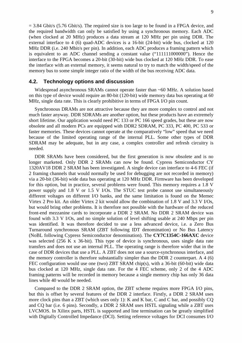
A slave SPI interface is implemented in FPGA logic for communication between that logic and the micro-controller. Four extra signals are placed so that all 8 pins of port 7 are used. The role of this path is not yet defined. The interfaces between the micro controller and the FPGA are shown in Fig. 10.
UC_DOUT
P7.0 SCK
4.7k
3V3_FPGA
UC_DIN
UC_EXT<3..0>
UC_CS_B
UC_SCLK
P7.1 MISO
P7.2 MOSI
P7.3 NSS
4.7k4.7k
P7.4 - P7.7
uC
0V_FPGA
FPGA
Fig. 10. Micro controller to FPGA SPI and extension interface.
Pin usage of micro controller IO ports 2 to 6 is described later in the text.
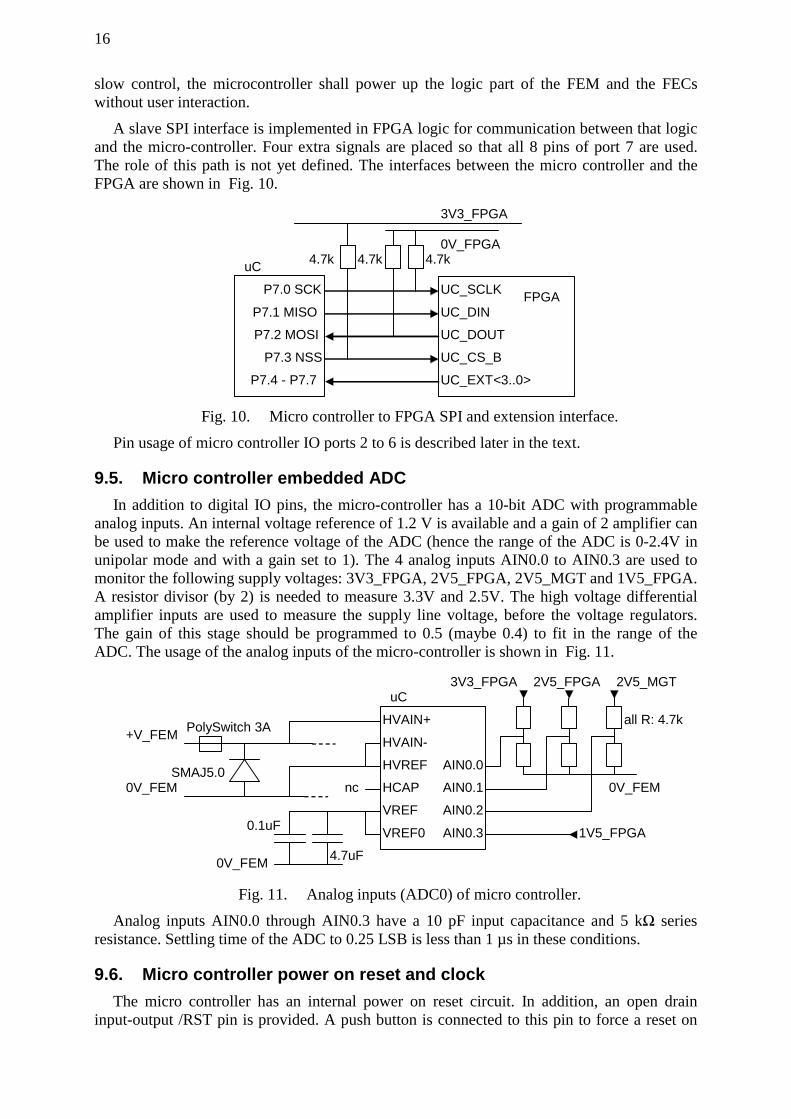
9.5. Micro controller embedded ADC In addition to digital IO pins, the micro-controller has a 10-bit ADC with programmable
analog inputs. An internal voltage reference of 1.2 V is available and a gain of 2 amplifier can be used to make the reference voltage of the ADC (hence the range of the ADC is 0-2.4V in unipolar mode and with a gain set to 1). The 4 analog inputs AIN0.0 to AIN0.3 are used to monitor the following supply voltages: 3V3_FPGA, 2V5_FPGA, 2V5_MGT and 1V5_FPGA. A resistor divisor (by 2) is needed to measure 3.3V and 2.5V. The high voltage differential amplifier inputs are used to measure the supply line voltage, before the voltage regulators. The gain of this stage should be programmed to 0.5 (maybe 0.4) to fit in the range of the ADC. The usage of the analog inputs of the micro-controller is shown in Fig. 11.
+V_FEM
0V_FEM
3V3_FPGA
PolySwitch 3A
SMAJ5.0
HVAIN+
HVAIN-
HVREF
HCAP
AIN0.0
AIN0.1
AIN0.2
AIN0.3VREF0
VREF
0V_FEM
2V5_FPGA 2V5_MGT
0V_FEM
0.1uF
4.7uF
nc
all R: 4.7k
1V5_FPGA
uC
Fig. 11. Analog inputs (ADC0) of micro controller.
Analog inputs AIN0.0 through AIN0.3 have a 10 pF input capacitance and 5 kΩ series resistance. Settling time of the ADC to 0.25 LSB is less than 1 µs in these conditions.
9.6. Micro controller power on reset and clock The micro controller has an internal power on reset circuit. In addition, an open drain
input-output /RST pin is provided. A push button is connected to this pin to force a reset on

17
the micro controller during debugging phases. In operation, if control over the network is lost, the only way to reset the micro controller is to cycle power. The MONEN pin is used to enable monitoring of the power supply of the micro controller. The datasheet recommends that this pin is set to VDD to enable monitoring.
The micro-controller has an internal ring oscillator and can optionally use an external RC circuit or crystal. Using CAN bus requires a precise time source, therefore the crystal option is selected. Details of the micro controller reset circuit and crystal are shown in Fig. 12.
Pushbutton
3V3_UC
0V_UC
/RST (uC_5)
4.7k
47k 1uF
XTAL2 (uC_27)
10M
XTAL1 (uC_26)MONEN (uC_28)
0V_UC 22pF
22pF
20MHz
Fig. 12. Micro controller reset and oscillator.
Selecting the frequency of the oscillator is partly determined by the CAN bus speed requirement. Using a 20 MHz system clock for the micro-controller and setting the Baud Rate Prescaler (BRP) to 4 gives a time quantum Tq = 200 ns. The maximum propagation delay of the slow control network is ~300 ns (60 m at 5 ns/m) plus ~200 ns (transceivers and optocouplers delay), i.e. ~1µs for round-trip. A reasonable rate for the CAN bus up to distances of 100 m is 500 kbit/s, i.e. a CAN bit time of 2 µs (or 10*Tq in our case). The Sync_Seg is fixed and equal to 1 Tq. The Prop_Seg can be set to 5*Tq (to accommodate 1 µs delay). The Phase_Seg1 and Phase_Seg2 are set to 2*Tq each. Hence the total of the 4 phases is 10*Tq, i.e. 2 µs which corresponds to the desired 500 kbit/s rate. For a more robust operation (with the same time quantum, Tq = 200 ns), one could set: Prop_Seg = 7*Tq = 1.4 µs, Phase_Seg1 = Phase_Seg2 = 6*Tq = 1.2 µs. This would make a CAN bit time of 20*Tq = 4 µs, i.e. a baud rate of 250 kbit/s.
9.7. Slow control CANbus Interface Ideally, there should be a galvanic isolation between FEM logic and the micro-controller
responsible for slow control. The number of interface signals is more than ~8 and using optocouplers would be too expensive. Hence, we propose to have no isolation between the micro-controller and the logic of the FEM, but only different voltage regulators, so that FEM logic can be powered-off while the slow control continues to run. Galvanic isolation is introduced at the level of the transceivers connected to the shared media of the slow control network. In this way, the front-end electronics of each detector module can remain electrically isolated (although all modules share the same ground, and several modules may be powered by the same low voltage power supply).
For the CAN bus interface, the same device that is used on the evaluation kit of the micro controller is selected: Texas Instruments SN65HVD230D. Optocouplers are used for galvanic isolation as shown in Fig. 13.

18
µCCANTX
CANRX
3.3V uC 180
3.3V CAN
4.7k CAN H
CAN L
3.3V CAN3.3V uC
4.7k
65HVD230
ACSL-6310
ACSL-6310
D
R
RS
180
Fig. 13. CAN bus isolated interface.
The selected part for the optocouplers is Avago Technologies ACSL-6310. This part includes 3-channels and can operate at up to 10 Mbaud, which is largely sufficient for CAN bus which runs at up to 1 Mbit/s. Two optocoupler channels are used to isolate the CANTX and CANRX pins. Note that the optocouplers make a non-inverting circuit. Connecting the CAN transceivers to the CAN controller via a non-inverting circuit is identical to the design of the micro-controller evaluation board (that does not have galvanic isolation). The third optocoupler in the package is used to provide failsafe operation when 3V3_UC is not present while 3V3_CAN is present. This is shown in Fig. 14.
ACSL-6310
0V uC
3.3V uC
3.3V CAN
4.7k
10k
RS180
Fig. 14. CAN power failsafe circuit.
When both 3V3_CAN and 3V3_UC are present, Rs is grounded on the CAN transceiver side through a 10 kΩ resistor. This enables the CAN output transceiver, with a slew rate controlled by the value of the resistor tied to Rs. When 3V3_UC is not present, but 3V3_CAN is present, Rs is tied to a high level and the CAN transceiver is disabled. The CAN bus continues to operate normally (obviously the non-powered module cannot be controlled). If 3V3_CAN is not present (independently of 3V3_UC), the corresponding device attached to the CAN bus cannot be controlled. If CAN transceivers are powered from different power supplies, the bus continues to operate if one or several transceivers is not powered (this is what is claimed in the datasheet of the transceiver).
9.8. Slow control MSCB interface As an alternative to CANbus, MSCB will be used in various other places in T2K 280 m
detectors. For compatibility, an optional MSCB interface is included on the FEM. Both CANbus and MSCB may be supported at the same time at the expense of additional components. MSCB uses RS-485 signalling in half-duplex mode. The selected transceiver is MAX3075EESA+. This part is RoHS compliant. It is a 3.3V device compatible with 5V devices and allows up to 256 transceivers on the same bus. The MSCB interface is shown in Fig. 15.

19
µCTX0
RX0
3.3V uC 180
3.3V MSCB
4.7k A
B
3.3V MSCB3.3V uC
4.7k
MAX3075
ACSL-6310
ACSL-6310
DI
RO
ACSL-6310
0V uC
(P1.6)
3.3V MSCB
4.7k
DE
180
180
DEP0.0
P0.1
¼ 74LV02A
RE
0V_MSCB
MSCB_DE
Fig. 15. MSCB interface.
The optocouplers on TX0 and RX0 make a non-inverting circuit. Termination resistors (120 Ω) must be placed only on the first node and last node of the multidrop bus. A termination connector with an embedded resistor shall be used on the last FEM (see below slow control connector section). Because MSCB is a half-duplex bus, an additional control line is needed to enable/disable transmission. An I/O line of the micro-controller is used for that purpose. In addition, this pin provides a failsafe circuit to avoid that the bus is hanged when the micro-controller side is powered off while other nodes on the bus are not. Because the micro-controller can only provide a low level when it is not powered, the opto-isolator used for DE necessarily makes an inverter circuit. A logic inverter is needed to revert back the signal to the desired active high level for enabling transmission. Note that a dedicated voltage regulator is used for the components located on the MSCB cable side (same type of circuit used for the CAN bus interface).
MSCB uses serial communication with 9 bit frames and therefore requires a 9-bit capable UART with address recognition features. The present implementation uses micro-controller UART0 in Mode 3 and timer 1, 2 3 or 4 for baud rate generation. Assuming a 20 MHz clock rate for the micro-controller and a target baud rate of 115.200 bauds, the closest achievable rate is: 20 / (16 x 11) = 113.636 baud, i.e. a deviation of -1.36% from the target. This deviation is not expected to cause synchronization difficulties.
During the layout phase of the full size FEM card, no sufficient board space was found to include both the CAN bus interface and MSCB interface. Decision was made to keep only the CAN bus interface and drop the MSCB interface.
9.9. Slow control network connectors and physical layer For the CAN bus baseline design, the standard DB9 connector and pinout defined in [6] are
recommended. The FEM is a so-called “bus node” and has 2 DB9 connectors (1 male and 1 female). Power for the CAN transceivers and the optocouplers is brought by the slow control cable (pin 9 of the DB9 connector). The exact type of cable for the slow control network is not yet defined. During the layout phase of the FEM card, it was found that DB9 connectors would take too much board space. Several other connectors have been defined for CAN bus,

20
although these are less common than DB9. For compactness, RJ45 connectors have been chosen. The selected part is a right angled, inverted type, RJ45 female header, pin through hole, part number MOLEX 438600001. This part is RoHS compliant. A disadvantage of RJ45 connectors over DB9 is the current capacity per pin. Electrical power is brought to 14 devices in each CAN bus chain. The selected RJ45 header is rated 1.5 A per pin. This should be sufficient, but if not, it is planned to use 2 power pins and 2 ground pins on the RJ 45 header. In such case, the use of RJ45 in our application would not be compliant with the CAN bus standard: one pin marked “reserved” in the standard would be affected to power.
For the MSCB option, a 10-wire flat ribbon cable and dual-row 2.54 mm header connector are used. The FEM board uses only the +5V power supply and it derives a +3.3V power supply from it. Other power lines (+15V and -15V) are not used but are connected for continuity with other devices in the chain that may use them. The Reset line, Interrupt and reserved lines are not used. The FEM board has 2 10-pin MSCB male headers: one for an incoming cable and one for an outgoing cable. If the node is the last one in the chain, a termination header is connected instead of the outgoing cable. The pinout of the MSCB connector is reproduced in Fig. 16 below.
Pin1 Pin2 Pin3 Pin4 Pin5 Pin6 Pin7 Pin8 Pin9 Pin10 Data A Data B -15V +15V +5V GND Reset Interrupt reserved reserved
Fig. 16. MSCB connector and cable.
Note that the MSCB option is no longer pursued and the information above is only informative.
10. On-board power supplies The FEM requires 2 different power supplies cables: 1 power supply cable for the
transceivers of the slow control network, and the main power supply cable of the FEM card (shared with the 4 or 6 FECs of the module).
The power supply for the slow control transceivers is common to all detector modules. It is used to power the CAN transceivers and one side of the optocouplers. The CAN transceiver has a maximum static current of 17 mA at 1 Mbps. Presumably, this number takes into account the load (60 Ω) on the CAN side, but not the user load output R (-8 mA sinked for a low level). In total, the current drawn by the CAN transceiver logic is modest: less than 100 mA. Using a DC/DC converter to derive 3V3_CAN power supply from the main power input of the detector module may be difficult if the supply voltage is below 5 V. Also DC/DC converters are not very cheap, and internal switching of high currents could interfere with the highly sensitive front-end pre-amplifiers. Hence using a common power supply for all 3V3_CAN is preferred. On each module, a LDO regulator is placed.
The main power supply input of the FEM card produces the following voltages: • +3.3V for the microcontroller of the slow control network and logic (3V3_UC), • +3.3V for part of the FEM logic and the corresponding FPGA I/Os (3V3_FPGA), • +2.5V for some of the FEM logic and FPGA I/Os (2V5_FPGA), • +2.5V for the RocketIO transceiver (2V5_MGT),

21
• +1.5V for the core of the FPGA (1V5_FPGA).
The power consumption of the micro-controller core is only 10 mA at 2.7V, 25 MHz. Most of the additional current is drawn by the I/O pins. Most have a low toggling rate or are kept static. The drive current of the PhotoMOS relay is 2 mA. Assuming 2 relays per FEC and a 6 FEC configuration, the static current is 24 mA. Each silicon ID chip requires a maximum of 100 µA when active. In total, ~1 mA can be taken by the ID chips. The MAX 1299 ADC requires 500 µA when active. The drive current for the LED of the optocoupler is 8 mA. At most, the 2 optocouplers powered from 3V3_UC draw 16 mA. In total, the current for the 3V3_UC supply is under 100 mA.
A fraction of the logic of the FEM uses 3.3V signalling. This includes all the logic to fanout the signals to the front-end ASICs and interface to the FECs. The LVDS fanout circuit for SCA_WCK and SCA_RCK draws ~14 mA per FEC. Other signals have a low toggling rate (except ADC_CLK) and will not need very much. The optical transceiver is also powered from the same 3.3V supply. The maximum current drawn by the device is 210 mA. The total current needed from 3V3_FPGA is ~310 mA for the 6 FECs option.
Because there is not much price difference between a 200 mA LDO and a 500 mA device, the same part number is used for 3V3_UC and 3V3_CAN power supplies. The selected device is Texas Instruments TPS77633PWP (500 mA capacity). For the 3V3_FPGA power supply, a 500 mA may only be marginally sufficient. The pin compatible TPS76833QPWPG4 device is used to provide a higher current capacity of 1A. Alternatively, the TPS77833 (0.75 A) could be used. Note that higher current devices, the TPS75333 (1.5 A) and the TPS75433 (2 A) are not pin compatible with the other devices. All parts are RoHS compliant.
The logic on board the FEM that uses 2.5V power supply includes: the SRAM memory buffers, the configuration PROM, the JTAG circuitry, the VCCAUX pins of the FPGA, and the reference oscillator(s). The operating supply current per RAM specified in the datasheet is 180 mA (for 166 MHz operation, while in our case we run at 120 MHz) excluding the I/O current. Assuming a read operation where 50% of the data pins toggle at each clock cycle (36 pins and 60 pins for the 4 FEC and 6 FEC schemes) with a 10 pF load on each pin (maximum input capacitance per pin given in Xilinx Virtex-II Pro datasheet), the dynamic current for memory output is 54 mA (4 FECs) and 90 mA (6 FECs). The dynamic current for the address, clock and memory control is supplied by the FPGA: ~20 pins, 50% toggle rate, 5 pF load per memory package. For write operations, the data bus current is also supplied by the FPGA. The estimated dynamic current is 27 mA (4 FECs) and 45 mA (6 FECs). The dynamic current for RAM addressing is 15 mA per RAM package. The total current estimate for the memory buffer of the FEM (in read) becomes 250 mA (4 FECs) and 480 mA (6 FECs). The VCCAUX pins of the FPGA have a quiescent current of 50 mA for the XV2VP4 device according to the datasheet but XPower gives 167 mA. In addition, a startup current of at least 250 mA should be supplied. The supply current for the on-board oscillator is 63 mA (for F > 80 MHz and including load, see datasheet). The configuration PROM current is 10 mA (core) + 10 mA (serial I/O), but this should not be active simultaneously with the memory buffer. The VCCO supplies of the FPGA also have a quiescent current: 1-8 mA according to the datasheet (per bank?) while XPower indicates ~187 mA. The total current estimate for 2V5_FPGA supply in normal operation (i.e. except during the power-up phase and configuration) is ~900 mA (6 FECs). To have a sufficient safety margin, a 2 A LDO regulator is preferred. The selected part is Texas Instruments TPS75425QPW. This part is RoHS compliant.
The RocketIO transceiver requires its own dedicated voltage regulator and passive filtering circuit. Refer to [5] for details. The maximum dissipation of the transceiver at 2.5 Gbis/s is 310 mW, i.e. 125 mA. Hence a 0.5A voltage regulator is sufficient. Taking into account the recommendation of Xilinx on the device family, the selected part number is Texas

22
Instruments TPS79525DCQG4 (available: Farnell France, 1.37€ per unit). This part is RoHS compliant.
The core of the FPGA requires 1.5V power supply. The quiescent current of a XC2VP4 device is 30 mA typical and 500 mA maximum (!). The dynamic power consumption is estimated with Xilinx XPower tool. Setting activity rates is not always very easy (long list with obscure signal names). The numbers found are 30 mA for quiescent current (identical to the typical value given in the datasheet), and 415 mA for the dynamic current. For future expansion, it can be assumed that the PowerPC processor is used. The dynamic power of the processor is 0.9 mW/MHz, i.e. 180 mW at 200 MHz (120 mA from 1.5V supply). The rough estimate for the current to supply is core is 0.5-1 A depending on which number to trust. To provide a sufficient margin, a 2 A LDO is chosen. The selected part is Texas Instruments TPS75415QPWP. This part is RoHS compliant.
The total estimate of current and power dissipation of the FEM is shown in Table. II. Using a switching DC/DC converter for the 1.5V power supply (and possibly for the 2.5V) would reduce power dissipation compared to using LDOs. However, switching high currents close to sensitive front-end devices might cause problems. Dual footprints are made on the prototype FEM to support both schemes (LDOs and DC/DC converters).
Table. II. FEM power estimate summary (6 FECs option).
Supply voltage Current estimate (A) Net Power1 (W) Supply power2 (W)
3V3_CAN or 3V3_MSCB 0.1 0.33 0.4
3V3_UC 0.1 0.33 0.4
3V3_FPGA 0.35 1.15 1.4
2V5_FPGA 0.9 2.25 3.6
2V5_MGT 0.125 0.3 0.5
1V5_FPGA 1 1.5 4
Total 2.575 5.9 10.3
The simplified power circuit for the slow control network transceivers of the FEM is shown in Fig. 17. Although distinct footprints for both CANbus and MSCB options are available, only one type of interface may be used. For the first prototype of the full size FEM, both voltage regulators may be placed to test the two different slow control network options. During the layout phase of the FEM, board space limitations imposed to retain only one option for the slow control network. CAN bus was selected and all the circuitry associated to MSCB was removed.
TPS77633 3V3_CANEN
IN
0V_CAN
5V_CAN
0V_CAN
PolySwitch 1A
SMAJ5.0
Fig. 17. Slow control transceivers power supplies.
The simplified power circuit of the full size FEM is shown in Fig. 18.
1 Power dissipated in the active components excluding the LDO regulators. 2 Total power dissipated on-board assuming a 4V external power voltage.

23
TPS77633
3V3_UC
EN
IN
0V_FEM
5V_FEM
0V_FEM
TPS77633
TPS75425
TPS75415
TPS79525
3V3_FPGA
2V5_FPGA
1V5_FPGA
2V5_MGT
EN
EN
EN
EN
3V3_UC
3V3_UC0V_UC
FEM_PDWN(uC_P6.6)
74LVC06A
PolySwitch 3A
SMAJ5.0
20 m
20 m
20 m
PG
PG
PG
uC_P6.7
Fig. 18. FEM on-board power supplies (LDO scheme).
On both power inputs, a reset-able fuse (Tyco PolySwitch RUEF300 for the 3A version and Raychem SMD100F for the 1A version) and a reverse over voltage protection diode (Vishay SMAJ5.0) are placed. At the input of voltage regulators producing a given output voltage, a 20 mΩ resistor (Welwyn OARS1 series) is inserted for current measurement. All regulators have a built-in back current protection diode and need not an external protection. The CAN transceivers and the slow control micro-controller voltage regulators are always enabled. All the voltage regulators powering the FPGA logic can be controlled by the micro-controller. While all regulators have an active low enable pin, the TPS79525 have an active high enable. Therefore an inverter is needed. When the micro-controller is not configured, all FEM regulators are enabled. This default state simplifies debugging of the FEM without the needed of a slow control operation to power-up the card. The Power Good outputs of the regulators controlled by the micro-controller are tied together pulled-up and can be read-out by the micro-controller. When any regulator is disabled, its PG pin goes to a low impedance state. When all regulators are operating normally, all PG pins are put in a high impedance state and PG goes high. For simplicity de-coupling capacitor are not shown.
As an alternative to LDOs, DC/DC converters may be used for the 2 devices that have the highest heat dissipation. The selected part is the PTH07070WAZT from Texas Instruments. This device can provide up to 3 A with 85-90% efficiency. Assuming a 4 V input and 1 A current for the 1.5 V supply; the heat dissipation of the LDO is 2.5W while it is ~0.25 W for the DC/DC converter. The cost is ~10 € (LDO scheme: ~3 €). The power circuit based on DC/DC converters is shown in Fig. 19.
PTH04070W
1V5_FPGA or2V5_FPGA
REG1V5_INor REG2V5_IN
0V_FEM
47 µFVo
GND
Vi
Voadj.Inh.BSS138N
FEM_PDWN
47 µF
11k (1.5V)2.2k (2.5V)
Fig. 19. FEM power supplies (DC/DC converter option).

24
Note that the selected DC/DC converter does not have a “power good” output. To verify that the device(s) is (are) operating properly, it will be necessary to acquire via slow control the measured output voltage. The DC/DC converter needs a discrete transistor to control the inhibit pin; the datasheet states that the inhibit pin of multiple devices cannot be tied together and that no pull-up resistor shall be placed. A resistor is needed to control the output voltage; using a 1% 0603 SMT resistor is adequate. A 11 kΩ resistor leads to a theoretical output voltage of 1.52 V and a 2.2 kΩ resistor leads to 2.54 V. High quality ceramic capacitors are required at the input and output: 47 µF, 6.3V, X5R SMT devices in 1210 package are selected.
10.1. Power-on configuration and reset When the FEM board is powered-up, the firmware is automatically loaded in the FPGA. In
addition, a force re-load can be initiated by the micro-controller over the slow control network. The state of the DONE pin can be monitored and a visual indicator is placed. The configuration circuit is shown in Fig. 20.
INIT_B
D0
4.7k
Pushbutton
3V3_UC
FPGA_PROG(uC_P2.4)
74LVC06A
2V5_FPGA
M0
CCLK
DONE
PROG_B
M2
M1
DIN
CCLK
RESET/OE
CF
0V_UC
4.7k330
PROM
CS_B
3V3_UC
FPGA_DONE_B(uC_P2.5)
LED
JP
330
0V
CE
330
WR_B
HSWAP_ENPWRDWN_B
open
VBATT
74LVC06A Fig. 20. Power-on configuration circuit.
When the micro-controller is not programmed, the FPGA_PROG pin is pulled down and PROG_B is pulled up (to 2.5V – this pin is not 3.3V tolerant). This allows the configuration PROM to pulse CF bar low and start self configuration. In addition, a push button is placed to manually re-load the firmware. When the FPGA is not configured, DONE is low, FPGA_DONE_B is high and the LED does not illuminate. When the FPGA is configured, DONE is pulled up high (at 2.5V). This should be sufficient to toggle the output of the inverter (the datasheet of the 74LVC06A states VIH min = 2 V when VCC = 2.7 V to 3.6 V) which goes low. Consequently, the LED illuminates and FPGA_DONE_B goes low. A jumper on M0 and M2 can be used to select the configuration source. When the jumper is un-installed (default), the FPGA is in Master Serial configuration mode (i.e. automatic configuration from the PROM). When installed, the FPGA is in JTAG mode. This mode is used for debugging. The pins HSWAP_EN and PWRDWN_B are internally pulled-up. The pin VBATT is tied to 0V because bit stream encryption is not used.
User logic configured in the FPGA has an active high RESET pin and active high ERROR indicator. The RESET pin can be activated by the micro controller or manually. The ERROR signal can be read by the micro controller. Note that these 2 signals are 3.3V I/Os and can be interfaced to the micro controller directly. This is shown in Fig. 21.
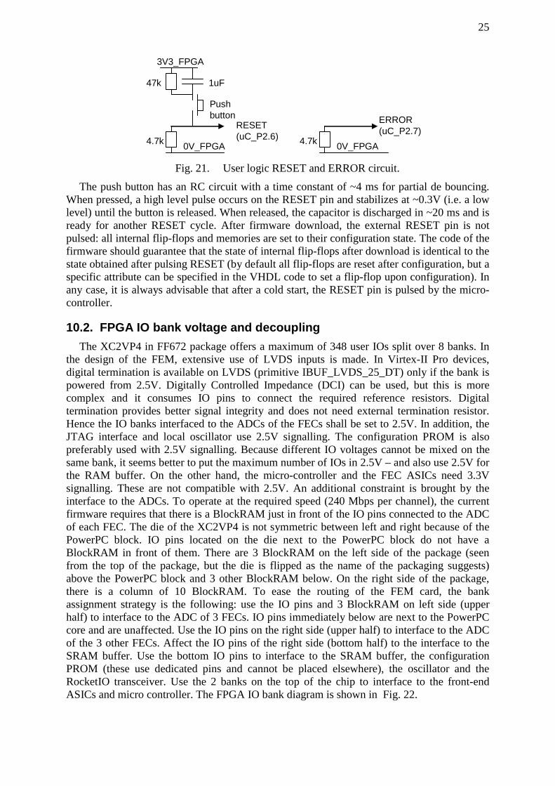
25
Pushbutton
3V3_FPGA
0V_FPGA
RESET(uC_P2.6)4.7k
47k 1uF
0V_FPGA4.7k
ERROR(uC_P2.7)
Fig. 21. User logic RESET and ERROR circuit.
The push button has an RC circuit with a time constant of ~4 ms for partial de bouncing. When pressed, a high level pulse occurs on the RESET pin and stabilizes at ~0.3V (i.e. a low level) until the button is released. When released, the capacitor is discharged in ~20 ms and is ready for another RESET cycle. After firmware download, the external RESET pin is not pulsed: all internal flip-flops and memories are set to their configuration state. The code of the firmware should guarantee that the state of internal flip-flops after download is identical to the state obtained after pulsing RESET (by default all flip-flops are reset after configuration, but a specific attribute can be specified in the VHDL code to set a flip-flop upon configuration). In any case, it is always advisable that after a cold start, the RESET pin is pulsed by the micro-controller.
10.2. FPGA IO bank voltage and decoupling The XC2VP4 in FF672 package offers a maximum of 348 user IOs split over 8 banks. In
the design of the FEM, extensive use of LVDS inputs is made. In Virtex-II Pro devices, digital termination is available on LVDS (primitive IBUF_LVDS_25_DT) only if the bank is powered from 2.5V. Digitally Controlled Impedance (DCI) can be used, but this is more complex and it consumes IO pins to connect the required reference resistors. Digital termination provides better signal integrity and does not need external termination resistor. Hence the IO banks interfaced to the ADCs of the FECs shall be set to 2.5V. In addition, the JTAG interface and local oscillator use 2.5V signalling. The configuration PROM is also preferably used with 2.5V signalling. Because different IO voltages cannot be mixed on the same bank, it seems better to put the maximum number of IOs in 2.5V – and also use 2.5V for the RAM buffer. On the other hand, the micro-controller and the FEC ASICs need 3.3V signalling. These are not compatible with 2.5V. An additional constraint is brought by the interface to the ADCs. To operate at the required speed (240 Mbps per channel), the current firmware requires that there is a BlockRAM just in front of the IO pins connected to the ADC of each FEC. The die of the XC2VP4 is not symmetric between left and right because of the PowerPC block. IO pins located on the die next to the PowerPC block do not have a BlockRAM in front of them. There are 3 BlockRAM on the left side of the package (seen from the top of the package, but the die is flipped as the name of the packaging suggests) above the PowerPC block and 3 other BlockRAM below. On the right side of the package, there is a column of 10 BlockRAM. To ease the routing of the FEM card, the bank assignment strategy is the following: use the IO pins and 3 BlockRAM on left side (upper half) to interface to the ADC of 3 FECs. IO pins immediately below are next to the PowerPC core and are unaffected. Use the IO pins on the right side (upper half) to interface to the ADC of the 3 other FECs. Affect the IO pins of the right side (bottom half) to the interface to the SRAM buffer. Use the bottom IO pins to interface to the SRAM buffer, the configuration PROM (these use dedicated pins and cannot be placed elsewhere), the oscillator and the RocketIO transceiver. Use the 2 banks on the top of the chip to interface to the front-end ASICs and micro controller. The FPGA IO bank diagram is shown in Fig. 22.

26
ADC of FEC#0, 1, 2
Bank 027 I/O max.
3.3V
Bank 127 I/O max.
Bank 260 I/O max.
Bank 360 I/O max.
Bank 427 I/O max.
Bank 527 I/O max.
Bank 760 I/O max.
Bank 660 I/O max.
3.3V
2.5V
2.5V2.5V
3.3V
2.5V 2.5V
ADC of FEC#3, 4, 5
RAM buffer
RAM bufferConfig PROMOscillator,Optical transceiver
Debug I/Oand spares
Pin A1
FF672 (XC2VP4) top view FEC ASICs andMicro-controller
Fig. 22. FPGA bank usage diagram.
The equivalent number of power/ground pairs for banks #0, #1, #4 and #5 is 4. For banks #2, #3, #6 and #7 it is 6 (see Xilinx Virtex-II Pro user guide). The bank that has the largest number of outputs is bank #6. Assuming that all 60 bank pins are outputs, the SSO limit is reached for LVCMOS 2.5V fast 12 mA buffers or LVCMOS 2.5V slow 16 mA buffers. It is expected that lower drive buffers are used for the memory. Therefore the SSO limit should not be reached. Table. III shows the global usage of FPGA I/O pins.
Table. III. Bank user I/O pin usage and direction.
Bank # IN OUT I/O SSO SSO budget Total pin Unused pin Bank usage
0 3 21 0 21 40 (53%) 24 3 89%
1 5 18 0 18 40 (45%) 23 4 85%
2 36 0 0 0 60 (0%) 36 24 60%
3 11 21 0 21 60 (35%) 32 28 53%
4 2 9 0 9 40 (22%) 11 16 41%
5 4 20 0 20 40 (50%) 24 3 89%
6 0 0 60 60 60 (100%) 60 0 100%
7 36 0 0 0 60 (0%) 36 24 60%
Total 97 89 60 - - 246 102 70%
Note that the pins INIT_B, DIN and DOUT for programming the FPGA use general purpose I/O pins located in bank #4. Bank #5 has the programming pins CS_B and RD_WR_B. Other programming pins are dedicated ones that need not be included in bank usage count. RocketIO pins are also dedicated pins. In the table, the SSO budget assumes that 12 mA buffers are used. This assumption is conservative. It should also be noted that all outputs have been taken into account in the SSO calculation, although some outputs are almost static or have a very low toggle rate. The number of decoupling capacitors per VCCO bank is shown in Table. IV. The number of capacitors is determined by the percentage of SSO budget multiplied by the number of VCCO pin of the bank (i.e. 7) as explained in [7]. The

27
number is increased to have at least one capacitor in each decade per bank, except for lightly loaded banks. Efforts are made to add more capacitors on bank #5 and #6.
Table. IV. Bank VCCO decoupling capacitors.
Bank # #of capacitors 10 nF 100 nF 1 µF 10 µF 220 µF
0 3 0 1 1 1 0
1 3 0 1 1 1 0
2 2 0 1 0 1 0
3 3 0 1 1 1 0
4 3 0 1 1 1 0
5 5 1 1 1 1 1
6 8 2 2 2 1 1
7 2 0 1 0 1 0
Total 29 3 9 7 8 2
For decoupling VCCINT, Xilinx specifies that one capacitor per pin must be used. There are 24 VCCINT pins on the FF672 package (6 pins at each corner). Each corner is decoupled with an identical set of decoupling capacitors except one corner where the largest capacitor could not be placed on the board. This is listed in Table. V.
Table. V. VCCINT decoupling capacitors.
Corner # #of capacitors 10 nF 100 nF 1 µF 10 µF 220 µF
0, 1, 2 5 1 1 1 1 1
3 4 1 1 1 1 0
Decoupling VCCAUX requires also one capacitor per pin. There are 12 VCCAUX pins on a FF672 package (3 at each corner). Each corner is decoupled with an identical set of decoupling capacitors as listed in Table. VI. Note that the VCCAUX pins power DCMs and must therefore be cleanly decoupled.
Table. VI. VCCAUX decoupling capacitors.
Corner # #of capacitors 10 nF 100 nF 1 µF 10 µF 220 µF
0, 1, 2, 3 4 1 1 1 1 0
For decoupling RocketIO devices, the recommendations of Xilinx must be strictly followed. Refer to [5] for details.
11. Debug and expansions I/Os
11.1. Expansion RS-232 Terminal The current design of the firmware of the FEM does not use the embedded PowerPC
processor of the FPGA. If it is used in the future, debugging the embedded software is a lot easier with a RS-232 terminal. The circuit given in Fig. 23 is used to interface to a terminal.

28
0V_FEM
C1+
C1-
C2+
C2-
R1OUT
T1IN
3V3_FEM
CONS_TX_B
EN
FORCEON
V+
V-
INVALID
FORCEOFF
Vcc GND0.1uF
0.1uF
0.1uF
0.1uF
0.1uF
T1OUT
R1IN
3V3_FEM
MAX3221
CONS_RX_B
CONS_TX
CONS_RX
n.c.
0V_FEM Fig. 23. Optional RS-232 terminal interface.
On the terminal side, a standard non-crossed DB-9 connector and cable are used. On the FEM side, using a DB9 connector is more than what is needed: this interface is optional, and even if it is used, it can only be used for debugging the board in a laboratory setup. Therefore, the FEM side uses a space and cost-saving 4-pin 2.54 mm header (1 ground at each end, 1 TX, 1 RX). A standard RS-232 cable will be cut and a 4-pin female connector will be soldered to plug onto the 4-pin header of the FEM card. The selected part for the RS-232 driver is the MAX3221CAE+. This optional part and the corresponding pin header may only be soldered on the prototypes of the FEM. During the layout phase of the FEM, board space limitations imposed to suppress this option. If a RS-232-terminal is needed, the corresponding circuitry will be placed on a small extension card plugged onto the expansion connector.
11.2. Extension cable The distribution of the clock and trigger signals via optical links is limited in precision to
±1 clock cycle (i.e. ±16 ns or ±10 ns; see the relevant section in this document for more details). This may or may not be an issue depending on the sampling frequency of the pads. A calibration may be needed to determine the relative skew of the different FEMs. A possible scheme is to inject a completely asynchronous pulse signal to all FEMs simultaneously using a dedicated cable. The main drawback of the approach is that an extra service cable is needed on all FEMs and galvanic isolation between FEMs is lost. Opto-isolators are not sufficiently fast to guarantee reliable switching with ~ns precision. Analog Devices iCoupler technology components exhibit a maximum skew of ~15 ns. Texas Instruments capacitive isolators (e.g. ISO721) are adequate in terms of skew (3 ns maximum part to part), but cannot operate in a magnetic field greater than 1000 A/m. The best way to transport an asynchronous signal with ~ns order precision is to use baseband signalling in LVDS. A RJ45 connector header is placed on each FEM. Two pairs are coupled to the main FPGA via LVDS to LVDS repeaters; the 2 other pairs are not affected at present. These 2 pairs are routed to the expansion slot. The RJ45 cable optional circuit is shown in Fig. 24.

29
CBL_N<0>
EN
100
CBL_P<0>
GEN_IN_N
GEN_IN_P
DS90LV001TM
3V3_FPGA
0V_FPGA
20k
12k
CBL_N<1>
EN
100
CBL_P<1>
CBL_CLK_N
CBL_CLK_P
DS90LV001TM
3V3_FPGA
0V_FPGA
20k
12k
CBL_N<3..2>
CBL_P<3..2> Expansion slot
Fig. 24. RJ45 extension cable.
Each LVDS to LVDS repeater has a termination and optional external fail safe (low level) resistors. The selected part for the repeater is National Semiconductor DS90LV001TM. This part is RoHS compliant. The part number for the RJ45 header is MOLEX 85505-0013.
During the layout phase of the FEM, it was also found that this extension would require too much board space. This option has been suppressed in the design.
11.3. Debug pins and expansion slot A certain number of free FPGA I/O pins and micro controller pins are routed to the
connectors of an expansion slot. The expansion slot comprises 2 low profile female header connectors. A small daughter card can be added for adding any unforeseen circuit. During board debugging, a daughter card with connectors for a logic analyzer or an oscilloscope can be plugged. The signals available on the debug/expansion slot are given in Table. VII and Table. VIII.
Table. VII. Debug/expansion slot I/O signals – connector 1.
Name Direction Standard Pin Count Description
SYNCH_OUT O CMOS 3V3 1 Generic synchronization output
SPARE_OUT<15..0> O CMOS 3V3 16 Debug/expansion outputs
SPARE_IN<3..0> I CMOS 3V3 4 Debug/expansion inputs
3V3_FPGA - - 2 3.3V power (I/O bank FPGA)
0V_FEM - - 2 FEM logic ground
Table. VIII. Debug/expansion slot I/O signals – connector 2.
Name Direction Standard Pin Count Description
EXT_2V5<13..0> versatile CMOS 2V5 14 Expansion pins 2.5V
UC_P1_7 versatile CMOS 3V3 1 Microcontroller unused pins Port #1
CBL_P<3..2> CBL_N<3..2>
versatile LVDS 4 RJ45 extension cable
2V5_FPGA - - 2 2.5 V power (I/O bank FPGA)
3V3_UC - - 1 3.3V power (micro controller)
0V_FEM - - 3 FEM logic ground
The selected connectors should be cheap, compact and have a low stacking height. The selected part is Harwin 1 mm pitch M40 connectors, 25 circuits version: female part number: M40-6202546; male part number: M40-6002546 (female part: 1.49 € / unit per 100; male:

30
1.43 € / unit per 100; Farnell France as of October 2006). Due to board space limitations and routing difficulties on the full size FEM, only one debug/expansion connector was kept. Expansion connector #1 is retained while connector #2 is suppressed.
12. Variations for reduced FEM cards The reduced FEM cards use the FPGA device of the STUC test probe or that of the Memec
evaluation kit. Therefore, the adaptation cards do not include an additional FPGA. The STUC probe does not have a JTAG flash memory for storing the firmware, and the core FPGA is programmed via USB. The Memec kit has an on-board flash PROM and JTAG interface. The buffer memory is present on all versions of the FEM card. The optical transceiver is only present on the Memec kit. The STUC version communicates with the host PC via USB. The local oscillator need not be present on the reduced FEM cards because both the STUC probe and the Memec kit have on-board programmable oscillators. The glue logic, interface connector to one FEC, silicon ID number, monitoring ADC, debug pins, etc. are present on the reduced FEM cards. Power is supplied by the Memec kit. In the Stuc setup, the USB interface of the host PC cannot supply enough current, and an external power supply is needed. None of the 2 versions of the reduced FEM includes the micro-controller used for slow control. Initially, the FPGA was supposed to perform slow control and monitoring, but this was changed at a later stage in the design.
In addition to the signals/components used on the full size FEM card, the reduced FEM cards have a number of extra I/Os. These are listed in Table. IX.
Table. IX. List of I/O signals specific to reduced FEMs
Name Direction Standard Description
GEN_IN I CMOS 3V3 Trigger Pulser
SCA_START I CMOS 3V3 Start write operations in SCAs
SCA_STOP I CMOS 3V3 Stop writing in SCAs
SYNCH_SCA_WCK I CMOS 3V3 Synchronize SCA write clock
EVENT_TYPE<1..0> I CMOS 3V3 Event type
CLR_TIME_CNT I CMOS 3V3 Clear time stamp counter
CLR_EV_CNT I CMOS 3V3 Clear event counter
The GEN_IN input is used to fire the internal (or external) test pulser using an asynchronous input signal. The signals SCA_START, SCA_STOP, SYNCH_SCA_WCK, EVENT_TYPE, CLR_TIME_CNT, CLR_EV_CNT are used to emulate the synchronous path that will distribute trigger and synchronization information when several FEM cards need to be synchronized. These can also be used in a single FEM configuration, but these signals are re-timed with an internal reference clock.
All the 8 signals listed in Table. IX are buffered using a 74LVC244A before entering the FPGA of the reduced FEM. The external inputs GEN_IN, SCA_START and SCA_STOP are accessible through LEMO connectors, while the other signals are placed on a 2.54 mm header. On the full size FEM, the signal GEN_IN was suppressed. Originally, it was planned to transport it via the optional cable (RJ45) in LVDS and also feed it to the FPGA in LVDS. Two input pins on the FPGA had been allocated for this signal: GEN_IN_P and GEN_IN_N. This option is no longer pursued.

31
IV. Interface to Analog Front-end cards 1. Principles
The interface between the FEM card and the FECs is parallel and electrical. Each FEM serves 4 FECs in the baseline design, but this could be changed to 6 or even 8 FECs. The change must be anticipated at design time to minimize the impact on implementation. The interface transports fast LVDS signals (up to 120 MHz DDR), skew, jitter and latency critical signals (ADC and SCA clock and timing signals) and slow control signals. Because the FEM and the FEC will be powered by different voltage regulators, care must be taken to guarantee correct initialization and operation in the following situations. When one or several FEC is powered while the FEM is not yet powered, none of the FEC is allowed to attempt to drive any pin of the interface to a high level. In other words, there must not be any current sourced from the FECs to the FEM through the I/O interface when the FEM is not powered. The same holds true when the FEM is powered but not yet configured (the on-board FPGA I/O’s are tri-stated until the firmware has been successfully loaded). Reciprocally, when the FEM is powered while one or several FEC(s) is/are not powered, the FEM is not allowed to source any current to that/these FEC(s) through the I/O interface. This implies that all output signals from the FEM to each FEC is either low or tri-stated in this situation. FECs may be powered-off individually, in case of failure for example, or to isolate a mal-functioning FEC. When one or several FEC(s) is/are powered down, the rest of the system must continue to operate normally. This implies that none of the signals distributed from the FEM to the FECs can share a common bus line across all FECs, and all common signals must be buffered on a per FEC slot basis. At the different stages of the development of the system, it will also be useful to run a FEM that is not fully-equipped with all the FECs it would normally serve. This configuration corresponds to the test-bench of the front-end ASIC, the test of one FEC, or the test of partially equipped detector modules. When one or several FEC is not present, the FEM should operate with the actual number of operational FECs, should not distribute any signal to non-present FECs, and must not expect any response from non-present FECs.
The connector used for the interface between the FEC and the FEM should be sufficiently robust to survive multiple insertions and removal. Positioning is somewhat critical for the correct insertion of the FEM that will have 4-8 connectors. The candidate connector must be available in right-angled version for the final system, but also in straight version for the test bench of the front-end ASIC and the test bench of the FEC. The number of circuits must be sufficient to provide enough grounds for shielding and a few spare circuits for signals that were not initially anticipated.
The test bench of the ASIC and the test bench of the FEC must use exactly the same connector, with all the signals used by both types of card placed on the same pins. There may be extra signals specific to either setup, and these must be put in the inactive state (i.e. low or tri-state) when not used.
2. List of FEM / FEC interface signals The complete list of interface signals between the FEM and the FECs / front-end ASIC test
bench are listed in Table. X.
Table. X. FEM / FEC interface signal list
Name Dir3 Standard Description
General Control
3 Direction as seen on the FEM side; this is reverted on the FEC side.

32
REG_INH_B<(FEC-1)..0> O CMOS 3V3 Power down FEC Voltage Regulator
ADC_PDWN_B<(FEC-1)..0> O CMOS 3V3 Active low power down for the ADC
MM_POL<(FEC*2-1)..0> O CMOS 3V3 Set detector pad to ground or floating
SCA control
SCA_WCK_P<(FEC-1)..0> O
SCA_WCK_N<(FEC-1)..0> O
LVDS Tri-state
SCA Write clock; active on the rising-edge
SCA_WRITE<(FEC-1)..0> O CMOS 3V3 SCA Write Enable; active high
SCA_RCK_P<(FEC-1)..0> O
SCA_RCK_N<(FEC-1)..0> O
LVDS Tri-state
SCA Read clock; active on the rising-edge
SCA_READ<(FEC-1)..0> O CMOS 3V3 SCA Read Enable; active high
ADC signals
ADC_CLK<(FEC-1)..0> O CMOS 3V3 ADC clock; active on rising-edge
ADC_DCO_P<(FEC-1)..0> I
ADC_DCO_N<(FEC-1)..0> I
LVDS Tri-state
ADC data clock output
ADC_DATA_P<(FEC*4-1)..0> I
ADC_DATA_N<(FEC*4-1)..0>
I
LVDS Tri-state
ADC serial data output
ADC_FCO_P<(FEC-1)..0> I
ADC_FCO_N<(FEC-1)..0> I
LVDS Tri-state
ADC framing clock output
ADC_DTP<(FEC-1)..0> O Analog ADC Digital Test Pattern4
Slow control configuration
SCA_CS<(FEC*4-1)..0> O CMOS 3V3 Tri-sate
Active high Chip Select for each of the 4 ASICs of the FECs
SPI_SCLK<(FEC-1)..0> O CMOS 3V3 Tri-state
Serial clock input (common to all ASICs and test pulser DAC)
SPI_MOSI<(FEC-1)..0> O CMOS 3V3 Tri-state
Serial data input (common to ASICs and pulser DAC)
SCA_MISO<(FEC*4-1)..0> I CMOS 3V3 ASIC serial data output; each of the 4 ASICs uses a separate line
Calibration/Test pulser
GEN_GO<(FEC-1)..0> O CMOS 3V3 Tri-state
Active high Pulser command
GEN_CS<(FEC-1)..0> O CMOS 3V3 Tri-sate
Active high Pulser DAC chip select
- O - Pulser DAC serial clock input shared with the ASICs
- O - Pulser DAC serial data input shared with the ASICs
GEN_MISO<(FEC-1)..0> I - Pulser DAC serial data output
GEN_OUT I - Analog output of pulser (for future use)
4 See Analog Devices AD 9229 datasheet for details
33
Monitoring and others
FEC_ID<(FEC-1)..0> I/O CMOS 3V3 Tri-state
Interface to silicon ID chip, voltage and temperature monitor, using Dallas/Maxim 1-
wire protocol
MM_ID I/O CMOS 3V3 Tri-state
Silicon ID chip of Micromegas detector
FEC_PR_B<(FEC-1)..0> I CMOS 3V3 FEC presence detection
The total number of circuits is 41 per FEC, not including grounds and spare signals. The signals listed in Table. X are required when driving the FECs or the front-end ASIC testbench. Additional signals on the connector being discussed are specific to the testbench of the ASIC and shall not be used on the FECs. These signals are listed in Table. XI.
Table. XI. FEM / ASIC Testbench specific interface signal list
Name Dir5 Standard Description
Test Pulser
GEN_SEL O CMOS 3V3 Internal / External Pulser selection
The connector used to interface to the FEC is an 80-pin type. This provides ample shielding and grounding. A right-angled receptacle is mounted on the FEC. A straight pin header is mounted on the FEM. The product number on the FEM side is Hirose FX2CA-80P-1.27DSAL (71) and the RoHS compliant part is referenced 572-2357-7 71.
3. Distribution of output signals and multiplexing of input signals In order to reduce I/O pin count on the FPGA of the FEM, it is not desirable that this
FPGA device outputs directly all the signals needed for all FECs. Instead, some repeaters/buffers made with discrete logic are placed at the closest point to the interface connector of each FEC slot. To control easily the distribution of signals on a per FEC slot basis, the FPGA of the FEM produces a FEC_MASK bit pattern (one line per FEC). The FEC_MASK is a pattern read/write-able via slow-control used to enable or disable the distribution/reception of signals to/from each individual FEC. At power-up, and by default after FPGA firmware download, all FECs are masked, and operation cannot start until at least one FEC is un-masked.
3.1. General Control signals The voltage regulator of the front-end card has an enable pin. By default, the REG_INH_B
pin is pulled low on the FEC, and is set to a low level by the FEM after FPGA configuration. On the test board of the ASIC, the voltage regulator used is enabled when its control pin is low. Consequently, the voltage regulator is enabled by default. On the FEC, the voltage regulator is disabled when its control pin is low. Consequently, the FEC is disabled by default and remains in this state until the adequate operation is made on the FEM.
The AD9229 has an active high power down pin, PDWN. When this pin is high, the ADC is in power down mode and all data, DCO and FCO pins are placed in high impedance state. The power down feature of the ADC is used to avoid that the FECs source any current into the FEM when it is not powered. Obviously, the FEM card cannot drive a high level to the FECs when it is not powered, and the power down signal on the FEM side can only be active low. Hence an inverter is needed on the FEC. There should also be a pulldown resistor on the FEC side to assure that the FEC is in low power mode when no FEM card is attached. When 5 Direction as seen on the FEM side; this is reverted on the FEC side.

34
an FEC is masked, its ADC shall be placed in power down mode. The circuit used to enable/disable FECs is shown on Fig. 25.
ADC_PDWN_B(i)
3V3
pullup
FEC_MASK(i)
From FEM FPGA To FEC slot i
¼ 74xx02 R
0V
PDWN
FEC i
ADC_PDWN_B(i)
3V3
pullup
FEC_MASK(i)
From FEM FPGA To FEC slot i
¼ 74xx02 R
0V
PDWN
FEC i Fig. 25. ADC power down control.
During the layout phase of the full size FEM, gaining board space was found necessary. The capability to turn on/off the ADC independently of the voltage regulator of the FEC was suppressed. The pin ADC_PDWN_B is grounded on the full size FEM and the inverter placed on the FEC has been suppressed. The variations of hardware on the reduced FEM, full size FEM, ASIC test board and FEC are shown in Fig. 26.
ADC_PDWN_B(i)
3V3
FEC_MASK(i)FPGA
Register 0x4
Reduced FEM
PDWN
ASIC Test Board
REG_INH_B(i)FPGA
Register 0x5
ADC
LDO
ADC_PDWN_B(i)
Full size FEM
PDWN
FEC
REG_INH_B(i)µController P6.0-5
ADC
LDO
3V3
1 = down0 = active
1 = power on0 = power off
B24
B24
B3
B3
Fig. 26. Reduced FEM, FEM, ASIC Test board and FEC interoperability.
There are 4 possible combinations of board coupling: • Reduced FEM to ASIC test board: this was the initial thought that works fine, but
needs to be modified (see below). The capability to turn off the ADC is suppressed. • Reduced FEM to FEC: the output “ADC_PDWN_B” must no longer be connected to
the output of the NOR gate but must be grounded to enable the ADC on-board the FEC.
• Full-size FEM to ASIC test board: a hardware modification is needed on the ASIC test board. The ADC must be enabled. This can be achieved by removing the local inverter and connecting its output directly to the input.
• Full-size FEM to FEC: this does not require any hardware modification. The FEM board may not turn on power on any FEC before the FPGA is powered. This has to be guaranteed by the software running on the micro-controller.

35
3.2. SCA Control signals The distribution of SCA control signals in LVDS is done in several steps. The FPGA of the
FEM produces 2 copies of each signal (in unipolar LVCMOS 3V3 signaling): one copy is for the FECs placed on the left side, the other is for those placed on the right. Note that only one copy is available on the reduced FEM. On a per FEC slot basis, each signal is copied and translated to LVDS. Duplication (or bussing) of these signals to the 4 front-end ASICs of each FEC must be implemented locally on the FEC. The distribution circuit on the FEM card for one FEC slot is shown on Fig. 27. FECs located on the left use SCA_WCK(0) and SCA_RCK(0), while those located on the right use SCA_WCK(1) and SCA_RCK(1).
3V3
pullup
FEC_MASK(i)
SCA_WCK(0) or (1)SCA_RCK(0) or (1)
2SCA_WCK_P(i)SCA_RCK_P(i)SCA_WCK_N(i)SCA_RCK_N(i)
From FEM FPGA To FEC slot i½ DS90LV031B
EN_B
Fig. 27. Distribution of differential SCA control signals on the FEM.
When the FEM is not powered, no voltage is applied to the FEC through these lines. When the FEM is powered but not yet configured, LVDS buffers are placed in tri-state mode by the pullup resistor. When the FEM is configured but not yet programmed, all FEC_MASK are set to a high level and buffers remain in tri-state mode. Outputs become active on a given slot only when the corresponding FEC has been un-masked. The part that was originally selected is National Semiconductor DS90LV031. However, on the reduced FEM, it was found that this chip is heating abnormally. Replacing the chip by a new one did not improve the situation, and the same problem was observed by our Canadian colleagues. On a second instance of the reduced FEM, the equivalent device from Texas Instruments, SN65LVDS31 was used. This device does not exhibit the problem. The issue is not understood, and for the full size FEM, the part from Texas Instruments is strongly preferred.
The distribution of unipolar SCA control signals for one FEC slot is shown on Fig. 28. The full FEM produces 2 copies of the control signals, one for the left side FECs and one for those on the right. The reduced FEM produces only one copy. The local distribution on each FEC must be done locally. When the FEM is powered but not configured, FEC_MASK guarantees that all unipolar outputs are at a low level.
SCA_WRITE(i)SCA_READ(i)
3V3
pullup
FEC_MASK(i)
SCA_WRITE_B(0) or (1)SCA_READ_B(0) or (1)
2
From FEM FPGA To FEC slot i½ 74LVC02A
2
Fig. 28. Distribution of unipolar SCA control signals on the FEM.
FECs located on the left use SCA_WRITE_B(0) and SCA_READ_B(0), while those located on the right use SCA_WRITE_B(1) and SCA_READ_B (1).

36
3.3. ADC signals In the present design, the FPGA of the FEM produces one unipolar ADC clock signal per
FEC slot. The reason is to place the ADC_CLK output pin as close as possible (on the FPGA) to the pins that receives signals from the ADC. This helps in reducing skew problems, but may not be absolutely required. Because the differential read clock signal for the SCAs goes through a LVCMOS to LVDS translator (on the FEM) and a LVDS to LVDS fanout (on the FEC) before it reaches each front-end ASIC, some delay will be introduced. In order to compensate for part of this delay, an inverter is added on the ADC_CLK signal for each slot. Consequently, the FPGA of the FEM is required to produce an inverted clock for the ADC, i.e. ADC_CLK_B. The FEC_MASK signal is also used to mask the ADC_CLK signal, although this can also be done in the firmware of the FPGA. The distribution of the clock signal for the ADC of each FEC is shown in Fig. 29. A low level is applied to FECs when the FEM is power-up, configured, and these signals remain low until un-masked by a slow control operation. The delay introduced on the clock signal of the ADC depends on the part number used: the SN74LVC02A has a propagation delay of 3.6 ns typical, 4.2 ns maximum (at 3.3V and 25°C) while the SN74LV02A has a propagation delay of 5.6 ns typical to 7.9 ns maximum (at 3V3 and 25°C). The delay on ADC_CLK must approximately match the delay on the SCA_RD_CLK_P/N signals to guarantee that the ADC samples the analog output of the SCA after the longest stabilization period. The distribution of SCA control signals in LVDS takes ~4 ns and the internal delay within the ASIC has also to be taken into account. Hence, using the slower part, SN74LV02A, for the distribution of the clock to the ADC seems preferable. However, for reasons of availability, decision is made to use the SN74LVC02A on the full size FEM.
ADC_CLK(i)
3V3
pullup
FEC_MASK(i)
ADC_CLK_B(i)
From FEM FPGA To FEC slot i¼ 74LVC02A
ADC_CLK(i)
3V3
pullup
FEC_MASK(i)
ADC_CLK_B(i)
From FEM FPGA To FEC slot i¼ 74LVC02A Fig. 29. Distribution of the clock for the ADC of 1 FEC.
All signals received from the ADC on the FEM are routed directly to the FPGA of the FEM using 100 Ω differential lines terminated by a 100 Ω resistor. When one or several FECs is/are powered while the FEM is not powered, or powered but not configured, all ADC outputs must be in tri-state mode. This can be achieved by setting the ADC in power down mode. This capability is only available on the reduced FEM but had to be suppressed on the full size FEM to simplify the design of the PCB as much as possible. When connected to one or several FECs, the FEM should not enable the voltage regulators of the FECs unless it is powered. This is guaranteed by the REG_INH_B signal that disables the power on the FEC when low.
3.4. Test and configuration signals Because distributing slow control signals to each individual FEC slot directly would
require too many FPGA pins, a multiplexing scheme has been devised. In principle, all ASICs in all FECs will be programmed with the same parameters and writing these values in all ASICs on all FEC’s in parallel can be useful. Nonetheless, some parameters are specific and the capability to address each ASIC individually on any particular FEC is also needed. To fulfil these requirements, the FPGA of the FEM card produces a FEC_SELECT_B pattern, with one bit lane per FEC slot, to determine which FECs are concerned by the current slow

37
control operation. The appropriate selection pattern is written via slow control prior to any slow control operation on the FECs. Within the FPGA firmware, FEC_SELECT_B is AND’ed with FEC_MASK, so that none of the masked FEC can be selected.
On the AD9229, the DTP pin is used to serialize one of 2 test patterns on the data outputs of the device. This feature can be useful for debugging and is controllable by the FEM card. The DTP pin does not accept standard 2-valued logic levels, but needs either 0V, 1/3 Vdd, and 2/3 Vdd. The circuitry show on Fig. 30 is used to convert 2 standard logic outputs to 1 multi-valued output.
ADC_DTP(i)
3V3
pullup
FEC_SELECT_B(i)
ADC_DTP_B(1)
From FEM FPGA To FEC slot i½ 74LVC02A
R
2R
ADC_DTP_B(0)
ADC_DTP(i)
3V3
pullup
FEC_SELECT_B(i)
ADC_DTP_B(1)
From FEM FPGA To FEC slot i½ 74LVC02A
R
2R
ADC_DTP_B(0)
Fig. 30. Digital Test Pattern signal generation.
When an FEC is not selected, the ADC_DTP signal is low: this corresponds to the normal serialization of ADC data. For selected FECs, the state of ADC_DTP<1..0> will be converted to 4-valued logic to select a test pattern. Note that the test pattern will only be active while FEC_SELECT_B remains unchanged. Because FEC_SELECT_B needs to be modified for most configuration operations on the FECs, the test pattern cannot be sent indefinitely. Software must assure that ADC_DTP<1..0> are programmed back to “00” (i.e. normal ADC serialization) before exiting the relevant test procedure. Otherwise, any subsequent slow control operation on the ASICs will also instruct selected ADCs to output a test pattern. ADC_DTP_B<1..0> pins may have optional pullup resistors. This is not mandatory because the pullup on FEC_SELECT_B(i) will guarantee a low level on ADC_DTP(i) when the FEM is powered but not yet configured. On the full size FEM, the previous circuit is simplified to save 1 NOR gate. The signals ADC_DTP_B(0) are not used and the 2R resistor is grounded. Consequently only one of the 2 possible test patterns is accessible. The pattern “101010101010” is retained because it has a higher toggling rate. This may provide a better test pattern than “100000000000” that has fewer transitions (but this is not completely obvious).
The front-end ASICs and the test/calibration DAC on the FEC use a 4-wire serial protocol with one chip select line, one clock line, one serial data input line, and one serial data output line (this line may not be present for the test/calibration DAC). The clock and serial data input line can be common to all ASICs/DAC on all FECs provided that 5 individual chip select signals per FEC slot are generated. Including the test charge injector switch command, 8 slow control signals have to be sent from the FEM to each FEC. An octal non-inverting tri-state buffer per FEC slot is proposed for this function. This is shown on Fig. 31.

38
3V3
pullup
FEC_SELECT(i)
SCA_CS<3..0>GEN_CS
SPI_SCLKSPI_MOSIGEN_GO
8
From FEM FPGA To FEC slot i
74LVC244A
EN_BSCA_CS<3..0>(i)GEN_CS(i)SPI_SCLK(i)SPI_MOSI(i)GEN_GO(i)R
FEC i
8
0V
3V3
pullup
FEC_SELECT(i)
SCA_CS<3..0>GEN_CS
SPI_SCLKSPI_MOSIGEN_GO
8
From FEM FPGA To FEC slot i
74LVC244A
EN_BSCA_CS<3..0>(i)GEN_CS(i)SPI_SCLK(i)SPI_MOSI(i)GEN_GO(i)R
FEC i
8
0V
Fig. 31. Distribution of slow control signals.
The slow control serial data outputs of the front-end ASICs on each FEC should not be tied together (although these pins are in tri-state mode when the ASIC is not addressed) because nothing in the hardware prevents the user to erroneously initiate a slow control read operation to all 4 ASICs of a FEC. Consequently, each FEC outputs 4 slow control serial data output signals. These signals need to be multiplexed before entering the FPGA of the FEM to reduce I/O pin count. Any non-present or un-powered FEC should not disturb operation of these lines. For simplicity, only the ASICs of 1 FEC can be read-out at a time. A wired-OR based on open-collector inverter gates is used to combine the serial data output lines of each ASIC across all FEC slots as shown on Fig. 32. The same type of circuit is used to combine the serial output of the pulser, GEN_MISO, across all FEC to produce a single signal GEN_MISO_B, which is fed to the FPGA.
3V3
pullup
SCA_MISO_B<3..0>GEN_MISO_B
SCA_MISO<3..0>GEN_MISO
To FEM FPGA From each FEC
FEC*5*1/6 74LVC06A
0V
5*FEC
pulldowns
3V3
pullup
SCA_MISO_B<3..0>GEN_MISO_B
SCA_MISO<3..0>GEN_MISO
To FEM FPGA From each FEC
FEC*5*1/6 74LVC06A
0V
5*FEC
pulldowns
Fig. 32. Multiplexing serial data outputs from FECs.
When one or several FEC is/are not present or not powered, pulldown resistors tie the corresponding inputs to low level; hence the outputs of the corresponding inverters do not affect the state of the wired-OR. When the FEM card is not powered but one or several FEC(s) is/are powered, the respective serial data output pins are expected to be in tri-state mode (because none of the ASICs will have their chip select pin activated), and no current will be sourced to the FEM through these lines.
3.5. Signals specific to the testbench of the ASIC The test bench of the front-end ASIC can use an external pulse generator, in addition to the
internal one. The signal GEN_SEL is used to determine which pulse generator is used. The signal GEN_SEL is only present on the reduced FEM for controlling the testbench of the ASIC. The option to use an external pulser is not available on the FEC, and GEN_SEL shall be grounded on the full size FEM. The circuit given in Fig. 33 is used to buffer GEN_SEL on the reduced FEM.

39
GEN_SEL
3V3
pullup
FEC_MASK(0)
From FEM FPGA
¼ 74LVC02A R
0VASIC Test bench
GEN_SEL_B
Fig. 33. Circuit for pulser selection on ASIC testbench.
When FEC_MASK is floating or set, GEN_SEL is forced to 0. When FEC mask is cleared, the gate is an inverter for signal GEN_SEL_B. On the ASIC test bench card, when GEN_SEL is set to 0, the on-board pulser is activated; when GEN_SEL is set to 1, the external pulser is selected.
3.6. FEC, FEM and Micromegas detector Identification chips The detector module, each FEC and FEM has a unique identification number made by a
silicon ID chip from Dallas/Maxim (DS2438). This chip shall be powered in parasite mode from the D/Q pin. Assuming that the required pullup resistor on D/Q is placed on the FEM side, using the parasite power mode allows reading the ID and parameters of the FEC even when the card is not powered. It should be verified however that no current can be sourced to the VDD pin of the DS2438 through the D/Q pin when VDD is not powered (i.e. the FEC is not powered). When the FEC is powered but not the FEM card, the internal diode of the DS2438 prevents current from flowing through the DQ pin.
Each ID chip must be connected to the FEM card through a separate D/Q wire to be able to locate geographically each FEC. The FEM card also has its own ID chip; the same part number is used. Each ID chip D/Q pin is connected directly to one I/O pin of the micro controller of the FEM card, and has a 4.7 kΩ pullup resistor placed on the FEM side (to 3V3_UC).
3.7. FEC presence detection On the reduced FEM card, the silicon ID chip of the FEC and FEM are read out by the
FPGA. On the full size FEM, these (and the ID chip of the detector) are read out by the microcontroller dedicated to slow control. The full size FEM cannot easily detect which FEC cards are present. The pins FEC_PR_B are used for that purpose. This pin is grounded on the FEC. On the FEM side, each of these pins is pulled up separately using a 4.7 kΩ pullup resistor to 3V3_FPGA. When any FEC is not present, the FPGA will read a high level on the corresponding pin. If a FEC is present (powered or not), the FPGA will read a low level on the pin. The FPGA can use the 1-Wire controller developed for the reduced FEM to perform the read. Hence no change in the firmware is needed between the reduced FEM and the full size one.
V. FEM physical design aspects 1. Printed Circuit Board
The full size FEM uses a FPGA in a 1 mm pitch 672-pin BGA package and several other fine pitch integrated circuits. A variety of controlled impedance traces are needed. The operating frequency is 2 GHz for the optical transceiver links and 240 MHz for the interface

40
to the ADC of each FEC. Given the constraints of trace density and controlled impedance, a 12-layer class 7 PCB is found necessary. Minimum trace width is normally 100 µm with 120 µm spacing. Vias are 0.3 mm in diameter. The proposed board stacking is shown in Fig. 34.
1
2
3
4
5
6
7
8
9
10
11
12
Coating 15 µmCu 45 µmPrepreg 214 µmCu 18 µmLaminate 200 µmCu 18 µmPrepreg 174 µmCu 35 µmLaminate 110 µmCu 35 µmPrepreg 146 µmCu 35 µmLaminate 110 µmCu 35 µmPrepreg 146 µmCu 35 µmLaminate 110 µmCu 35 µmPrepreg 174 µmCu 18 µmLaminate 200 µmCu 18 µmPrepreg 214 µmCu 45 µmCoating 15 µmTOTAL: 2200 µm
TOP75 Ω uni.
GND
100 Ω diff. 50 Ω uni.
GND
Signal
Power
Power
Signal
GND
100 Ω diff. 50 Ω uni.
GND
100 Ω diff. 75 Ω uni.BOTTOM
Fig. 34. FEM board stacking - MCL-E-679F(J) material option.
Three layers are available for routing 100 Ω differential pairs: layer 3 and layer 10 are adequate for edge-coupled offset striplines while the bottom layer can have edge-coupled coated microstrip lines. In principle, these can also be implemented on the top layer, but in practice, the required vias for the BGA package obstruct routing. Some unipolar signals use a series source termination resistor driving a controlled impedance trace and the load. The preferred value for the impedance was originally 100 Ω. However, this value cannot be reached on the top, bottom or internal layers 3 and 10 because traces below 30 µm in width would be needed. Using layers 5 or 8 for 100 Ω unipolar traces is not possible without a substantial increase of the thickness of the PCB would be needed (~2.6 mm). It is therefore decided to use 75 Ω unipolar traces instead. These can be located on the top and bottom layers. A certain number of lines use 50 Ω series termination. These can be placed in internal layers 3 and 10, or eventually on the top and bottom layers. Note that the stacking is fully symmetric, as needed to guarantee a good planarity. The 2 external side laminates need to be rather thick to reach the desired impedance on layer 3 and 10. A relatively thin copper layer is preferred on layer 3 and layer 10 to increase the width of controlled impedance traces. Because layer 2 and layer 11 correspond to the other side of the laminate that carries layer 3 and layer 10, the thickness of the copper layer must be identical. Thicker copper layers adequate to carry power and ground currents are used on both sides of the 3 inner laminates. These 3 inner laminates and associated prepreg layers need not be as thick as the 2 external laminates and are chosen to reach a target total thickness of ~2 mm. The FEM will require a substantial force for insertion/extraction. Excessive bending can cause irreversible damages to the connections below the BGA package. The cooling plate of the FEM will also make a good mechanical stiffener, but it may not always be present, especially during the prototype phase and when debugging. The usual thickness of PCBs is 1.6 mm but this is not found sufficient.

41
A minimum of 2 mm is preferred. Excessive thickness is not a good option either: small diameter vias are more difficult to manufacture, weight and cost are increased. The proposed thickness is ~2.2 mm which seems to be a good compromise between the requirements for controlled impedance traces, a good rigidity, an acceptable weight and cost and limited risks concerning manufacturability.
The width of controlled impedance traces is computed using Polar Instruments field solver software CITS25 Version 2,0,3,0. Cadence tools also have their own tool. Results vary between the two software packages by up to ~10%. For illustration, a screenshot of the Polar tool is shown in Fig. 35.
Fig. 35. Screenshot of the Polar tool.
The parameters and computed impedance of the different controlled impedance traces are summarized in Table. XII.
Table. XII. Controlled impedance traces characteristics – MCL-E-679F(J) option.
Requirement Width (µm)
Thickness (µm)
Separation (µm)
Dielectric (µm)
εr Impedance (Ω)
100 Ω diff. bottom 95-100 45 120 214 + 15 4.2 100.07
100 Ω diff. Layer 3, 10 105-110 18 120 200 + 192 4.2 94
75 Ω uni. Top, bottom 115-120 45 - 214 + 15 4.2 76
50 Ω uni. Layer 3, 10 145-150 18 - 200 + 192 4.2 51
50 Ω uni. Top, bottom 345-350 45 - 214 + 15 4.2 50
The material used in the evaluation are the MCL-E-679F(J) Copper Clad Laminate and GEA-679F(J) Prepreg from Hitachi Chemical. The relative permittivity is the number quoted by the manufacturer when operating at 2 GHz (measured using a material analyzer). For lower operating frequencies, a different measurement method is used (“triplate line resonator”) which gives εr= ~4.6 at 250 MHz. However, the results given by the 2 methods are not compatible in the 800 MHz-1 GHz region where both measurements methods are used. Anyway, the impact of changing the relative permittivity in the proportion given above is rather marginal on the computed impedance (~2% decrease), and is probably negligible compared to the real accuracy of the prediction and the tolerance of the production process (±10 % based on the experience of the PCB manufacturer).
A second PCB manufacturer was contacted to get an alternative offer. The material proposed is referenced IT-180TC and is manufactured by Iteq. It appears that the projected

42
cost for producing ~80 boards using Hitachi material is ~50% higher than that of the other option: 110 € per unit versus 74 €. There do not seem to have any technical advantage that would justify choosing the most expensive option. Consequently, the board stacking and controlled impedance trace width have been reworked with Iteq material in mind. According to the PCB manufacturer, the parameters to take into account are εr= 4 for traces in the internal layers and εr= 4.5 for traces on the external layers. The board stacking that corresponds to IT-180TC material is shown in Fig. 36.
1
2
3
4
5
6
7
8
9
10
11
12
Coating 15 µmCu 40 µmPrepreg 220 µmCu 15 µmLaminate 200 µmCu 15 µmPrepreg 180 µmCu 30 µmLaminate 100 µmCu 30 µmPrepreg 130 µmCu 30 µmLaminate 100 µmCu 30 µmPrepreg 130 µmCu 30 µmLaminate 100 µmCu 30 µmPrepreg 180 µmCu 15 µmLaminate 200 µmCu 15 µmPrepreg 220 µmCu 40 µmCoating 15 µmTOTAL: 2110 µm
TOP75 Ω uni.
GND
100 Ω diff. 50 Ω uni.
GND
Signal
Power
Power
Signal
GND
100 Ω diff. 50 Ω uni.
GND
100 Ω diff. 75 Ω uni.BOTTOM
Fig. 36. FEM board stacking – IT-180TC material option.
The features of the controlled impedance traces are revisited in Table. XII. Note that the PCB manufacturer has slightly different recommendations for some trace width: 115 µm for 100 Ω differential traces in the internal layers; 365 µm for 50 Ω in the top/bottom layers; 175 µm for 50 Ω in the internal layers and 140 µm for 75 Ω in the bottom layer. The difference is probably marginal given that different tools were used and because of the tolerance of the process. Note that the same trace width and spacing are used independently of the selected material. The same Gerber files can be used and no re-engineering is needed when choosing between the 2 materials selected.
Table. XIII. Controlled impedance traces characteristics – IT-180TC option.
Requirement Width (µm)
Thickness (µm)
Separation (µm)
Dielectric (µm)
εr Impedance (Ω)
100 Ω diff. bottom 95-100 40 120 220 + 15 4.5 100.08
100 Ω diff. Layer 3, 10 105-110 15 120 200 + 195 4 98.59
75 Ω uni. Top, bottom 115-120 40 - 220 + 15 4.5 75.33
50 Ω uni. Layer 3, 10 145-150 15 - 200 + 195 4 53.05
50 Ω uni. Top, bottom 345-350 40 - 220 + 15 4.5 49.43

43
VI. FEM Firmware 1. Outline of the firmware
The central part of the FEM card is a large FPGA device that implements most of the logic functions performed by the card. The firmware is entirely written in VHDL and comprises synthesizable blocks as well as test bench files. A schematic view of the top level synthesizable entity is depicted in Fig. 37.
AcquisitionController
FEM Core
ADCInterface
RAMController
Slow controlRegisters
Packetizer
De-packetizer
Trans-ceiver
DataOrganizer
DataFilter
Tx in
Rx out
ADCInterfaceADC
InterfaceADCInterface
FEM FPGA
ZBT SRAM
FEC Data
OpticalModuleOr USB
ControllerTime-critical
signals
FEC/FEMSlow Control
ADC clock
Fig. 37. Block diagram of the FPGA logic of the FEM card.
The top level entity is a wrapper that adds I/O pads to a component that contains several blocks. The Transceiver block is the interface between the external optical module or USB controller and the core of the FEM logic. Two different implementations of the Transceiver block are provided: one is based on a RocketIO transceiver; one is made to interface to the USB controller of the STUC test probe. The RAM Controller is the interface between the core logic and the external memory. Initially, 2 versions were provided, one for ZBT type SRAMs and one for DDRII SRAMs, but only the ZBT option was pursued. The RAM Controller is in charge of serving read/write requests issued by the Core logic. The memory side operates at double speed compared to the internal side. The FEM Core is also organized in different modules. The Depacketizer block is responsible for receiving and decoding slow control and event data request packets as well as time critical trigger and synchronization signals. Decoded slow control requests are handled by the Slow control Registers block. Some outputs of the Slow control register block drive directly external pins, while some registers are used only internally. Time-critical signals are fed to the Acquisition Controller. This block is the main sequencer of the card. It generates all the necessary signals for clocking the read and write cycles of the SCAs, fire the test pulser, enable the ADCs, and generate memory addresses for the data capture and read-back phases. The ADC Interface block is duplicated 4 or 6 times depending on the number of FEC to control. Each of these blocks receives data from the ADC of a FEC and transports data from the external device clock domain (120 MHz DDR) to the common internal clock domain (60 MHz single data rate and consequently 4 times wider data path). Digitized and re-clocked ADC data are fed to the Data Organizer block. This block performs some de-serialization and re-ordering of ADC samples so that data storage and retrieval in the external memory is simplified. During the read-back phase, the

44
data fetched by the RAM Controller is processed by a Data Filter block. This block performs the final formatting of event data, including an optional zero-suppression before data is forwarded to the Packetizer block. The Packetizer block accepts two main data inputs: data from a slow control register or a fragment of formatted event data. Depending on whether the request was a slow control action or a request to return event data, the Packetizer block emits the corresponding packet header, inserts data from the appropriate input and appends the adequate trailer (e.g. CRC 32 placeholder and End of Packet comma character). The packet is handled by the transceiver block which performs 8B/10B encoding and serialization in the RocketIO implementation, and the adequate transmission over USB in the STUC probe implementation.
2. FEM Register map The control of programmable parameters on the FEM and FECs is done through read/write
registers accessible via a 16-bit address / 16-bit data bus. The list of registers defined at present is given in Table. XIV.
Table. XIV. FEM register map.
Address Width Access Description
0x00 16-bit W through Asynchronous trigger / Miscellaneous control
0x02 16-bit R/W Data Acquisition read back parameters
0x04 8-bit RO - R/W FEC Mask (1, 4 or 6 bit wide)
0x05 8-bit R/W FEC Power down (1, 4, or 6 bit wide)
0x06 8-bit R/W SCA Write clock divider
0x07 8-bit R/W ID Chip interface / FEC presence detection
0x08 16-bit R/W Pulser Control
0x0A 16-bit R/W Number of SCA cells to digitize (1-511)
0x0C 8-bit R/W Slow control ASIC Chip Select and pulser DAC Chip Select
0x0D 8-bit R/W FEC Select (1, 4 or 6 bit wide)
0x0E 8-bit R/W Slow control serial clock and master data output
0x0F 8-bit RO Slow control slave data output of ASIC, pulser DAC, monitoring ADC
0x10 8-bit RO Acquisition State / Gigabit link RX parity error count
0x11 8-bit RO Gigabit link RX packet format error count
0x12 16-bit RO Gigabit link RX packet count
0x14 16-bit R/W Read-back Offset in SCA cells
0x16 16-bit R/W SCA Stop delay
0x18 16-bit R/W Test data pre-load shift register for data/address
0x1A 16-bit R/W SCA end-of-write to start-of-read delay
0x1C-0x1F - - Decoded – reserved for future use
0x20-0x0FFF - - Unaffected
0x1000-0x1FFF
16*2048 R/W Sample re-order Look-Up Table
0x2000-0x3FFF
16*4096 R/W Pedestal Look-Up Table
0x4000- 16*4096 R/W Threshold Table
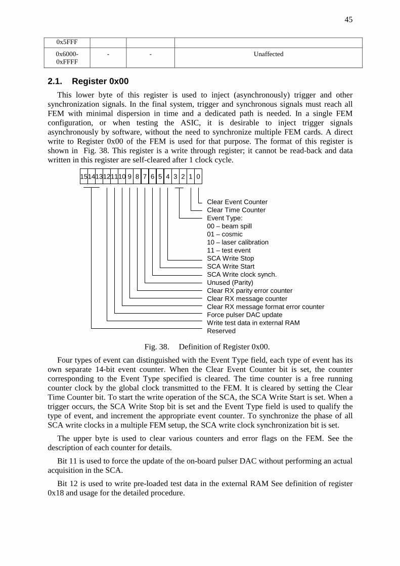
45
0x5FFF
0x6000-0xFFFF
- - Unaffected
2.1. Register 0x00 This lower byte of this register is used to inject (asynchronously) trigger and other
synchronization signals. In the final system, trigger and synchronous signals must reach all FEM with minimal dispersion in time and a dedicated path is needed. In a single FEM configuration, or when testing the ASIC, it is desirable to inject trigger signals asynchronously by software, without the need to synchronize multiple FEM cards. A direct write to Register 0x00 of the FEM is used for that purpose. The format of this register is shown in Fig. 38. This register is a write through register; it cannot be read-back and data written in this register are self-cleared after 1 clock cycle.
151413121110 9 8 7 6 5 4 3 2 1 0
Clear Event CounterClear Time CounterEvent Type:00 – beam spill01 – cosmic10 – laser calibration11 – test eventSCA Write StopSCA Write StartSCA Write clock synch.Unused (Parity)Clear RX parity error counterClear RX message counterClear RX message format error counterForce pulser DAC updateWrite test data in external RAMReserved
Fig. 38. Definition of Register 0x00.
Four types of event can distinguished with the Event Type field, each type of event has its own separate 14-bit event counter. When the Clear Event Counter bit is set, the counter corresponding to the Event Type specified is cleared. The time counter is a free running counter clock by the global clock transmitted to the FEM. It is cleared by setting the Clear Time Counter bit. To start the write operation of the SCA, the SCA Write Start is set. When a trigger occurs, the SCA Write Stop bit is set and the Event Type field is used to qualify the type of event, and increment the appropriate event counter. To synchronize the phase of all SCA write clocks in a multiple FEM setup, the SCA write clock synchronization bit is set.
The upper byte is used to clear various counters and error flags on the FEM. See the description of each counter for details.
Bit 11 is used to force the update of the on-board pulser DAC without performing an actual acquisition in the SCA.
Bit 12 is used to write pre-loaded test data in the external RAM See definition of register 0x18 and usage for the detailed procedure.

46
2.2. Register 0x02 This register is used to control the transfer of event data from the buffer memory of the
FEM to the transceiver sending data to the DCC. Refer to the description of the data retrieval phase for the signification of the bit fields shown in Fig. 39.
151413121110 9 8 7 6 5 4 3 2 1 0
Argument 1Argument 2CompressModeReserved
Fig. 39. Definition of Register 0x02.
To request a packet of data, the DCC simply writes into this register. This write operation is not echoed by a slow control response packet, but by a packet that contains the data samples determined by the supplied parameters.
2.3. Register 0x04 This register is used to mask FECs that are either non present or not active in a multiple
FEC setup. This modifiable part of this register is 1 bit, 4-bit or 6-bit wide depending on the version of the firmware. When a bit is set, the corresponding FEC is inactive. Its ADC is put in power down mode, and after a trigger, the FEM logic does not attempt to gain synchronization on the output stream of its ADC. After configuration or RESET, all FECs are masked and at least one FEC must be unmasked before operation.
7 6 5 4 3 2 1 0
Mask FEC #N:Bit #N = 0 – FEC activeBit #N = 1 – FEC disabled (default)FEC count supported:00 – illegal 01 – 1 FECs10 – 4 FECs11 – 6 FECs
Fig. 40. Definition of Register 0x02.
The two upper bits are read only. These are used to determine the actual number of FECs supported in the instant version of the firmware. It is expected that the application software reads this field before any attempt to modify other bits is made.
2.4. Register 0x05 This register is used to control the voltage regulators of the FEC to power up and down
each FEC individually. This register is 1 bit, 4-bit or 6-bit wide depending on the version of the firmware. This register is deprecated in full-size FEM: the on-board micro controller is used to perform the required function instead of the FPGA.
2.5. Register 0x06 This register is used to set the frequency of the clock for writing into the SCA. For a 60
MHz master clock setup, the write clock frequency is 60 MHz / (SCA write clock divider).

47
The value written in this register must be even; i.e. setting this register to 0x2 or 0x3 will lead to the same SCA write clock frequency of 30 MHz. In the setup with a 100 MHz master clock, the clock generator has been improved to support both even and odd dividers. The acceptable range is [2, 64] leading to clock rates of 50 MHz, 33.33 MHz, 25 MHz, … 1.5625 MHz. After power up, and whenever the content of this register is changed, it is required to re-synchronize the SCA write clock generated by all FEMs using the synchronous signal fanout network. Failure to due this will lead to an unpredictable phase shift between the SCA write clocks of different detector modules.
2.6. Register 0x07 This register is used to control the silicon ID chip of the FEM card. Access to the ID chips
is only possible on the reduced FEM. The on-board micro controller is used to perform the required function instead of the FPGA on the full-size FEM. Bit usage is given in Fig. 41.
7 6 5 4 3 2 1 0
Serial data Master In, Slave OutDevice BusyAction:00 – Reset / Presence01 – Read 10 – Write 011 – Write 1Device selectLoad Action
Fig. 41. Definition of Register 0x07.
On the full size FEM, write operations have no effect and both Reset and Read operations place in Bit 0 the state of the selected FEC_PR_B pin. This bit shall be “0” when a FEC is present and “1” otherwise. The Device select field allows addressing 8 one-wire devices. Device #0 corresponds to the silicon ID chip placed on the (reduced size) FEM, device #1 selects the ID chip of the Micromegas detector (when available), and sub-sequent devices correspond to the FECs.
2.7. Register 0x08 This register is used to control the pulser of the FEC.
151413121110 9 8 7 6 5 4 3 2 1 0
Pulser delayUse pulserPulser selection0 – on-board FEC pulser1 – external pulser
Fig. 42. Definition of Register 0x08.
The pulser selection bit is used to specify if the on-board FEC pulser or an external pulser is used. If any of the internal or an external pulser is used, the Use pulser bit must be set. Setting this bit will instruct the firmware to fire the pulser (internal or external) after the delay programmed in the Pulser delay field has elapsed. The pulser delay is expressed in units of the global reference clock period (i.e. 16 ns for a 60 MHz master clock). The time origin is taken from the last occurrence of both the SCA Write Start and SCA Write clock synchronization

48
events. This double synchronization is necessary to guarantee that the pulser is fired with a predictable delay with respect to the start of write into the SCA, and also a predictable delay with respect to the phase of the write clock of the SCA. It is also possible to update the value of the DAC pulser asynchronously by writing to the appropriate bit in register 0x00.
2.8. Register 0x0A This register is used to specify the number of SCA cells to digitize during the read-out
phase of the SCA. When a SCA Write Stop signal is issued (i.e. when there is a trigger), the FEM automatically applies the clock to the ADC of all non-masked FECs, waits until all ADCs have gained synchronization, and performs the readout of the SCA, storing the converted samples into the on-board FEM SRAM. All channels of the SCA must be read-out, but any number of time bins may be read-out. The firmware generates the desired number of cycles for a partial read-out of the SCA. The content of this register shall be set from 1 to 511. After the required number of time bins has been digitized, an additional cycle is always performed to digitize the encoded value of the last position of the write pointer of the SCA.
2.9. Register 0x0C This register is used to control the chip select of the serial interface of the FEC and various
other resources. The bit mapping is shown in Fig. 43.
7 6 5 4 3 2 1 0
FEC ASIC Chip SelectFEM ADC Chip SelectFEC Pulser DAC Chip SelectFEC ADC Digital Test Pattern00 – normal operation01 – “1000 0000 0000”10 – “1010 1010 1010”11 – restricted
Fig. 43. Register 0x0C definition.
The FEC ASIC Chip Select bit is used to drive the Chip Select pin of the slow control interface of each of the 4 ASICs of a FEC. The FEM ADC Chip Select bit is used to drive the chip select pin of the monitoring ADC on-board the FEM. The FEC Pulser DAC Chip Select bit drives the chip select pin of the pulser DAC of the FEC. Several ASICs may be selected simultaneously (to write the same data to several ASICs), but all other combinations of chip selection must be mutually exclusive. In a multi-FEC setup, the FEC_SELECT register (see below) must be programmed with the appropriate bit pattern to select one FEC among all the FECs that are present and not-masked.
The FEC ADC Digital Test Pattern bit field is provided for debug purposes. It selects the mode of operation of the output serializer of the ADC of the FEC.
2.10. Register 0x0D This register is used to control to which FEC the chip select bit pattern, serial data output
and serial clock should be applied. This register is 1 bit, 4-bit or 6-bit wide depending on the version of the firmware. To perform a slow control operation on the ASIC or the serial pulser DAC of a given FEC, this register must be set before applying the chip select pattern to the device and toggling the serial clock. Although programming several FECs in parallel is conceivable, it is recommended to set only 1 bit at a time in this register. After completion of

49
a slow control operation on a FEC, it is advised to reset all the bits of this register to avoid any potential interference with other slow control operations.
2.11. Register 0x0E This register is used to supply the serial clock and data output to write over the serial
interface for programming the ASICs, pulser DAC and monitoring ADC on-board the FEM. Bit usage is shown in Fig. 44.
7 6 5 4 3 2 1 0
Serial ClockSerial data Master Out, Slave InUnaffected
Fig. 44. Register 0x0E definition.
The serial clock on all devices controlled by this serial interface is active on the rising edge. After setting the appropriate FEC target (Register 0x0D) and chip select pattern (Register 0x0C), the control software should supply the first bit of data and set the clock to 0 during the first access to this register. Then it should perform a second access to set the clock to 1 without changing the value of the data bit, and perform a third access to set the clock back to 0 and supply the next bit of data. When all bits have been transferred, the chip select pattern should be cleared and all FECs de-selected.
2.12. Register 0x0F This register is used to read the serial data received from the ASICs, pulser DAC, or
monitoring ADC. Bit affectation is shown in Fig. 45.
7 6 5 4 3 2 1 0
ASIC Serial data Master In, Slave OutMonitoring ADC Serial data Master In, Slave OutMonitoring ADC Serial Strobe OutputPulser DAC Serial data Master In, Slave Outunaffected
Fig. 45. Register 0x0F definition.
The serial data output of the 4 ASICs of a FEC are assigned to a different bit in this register and it is in principle possible to perform a slow control read operation of all 4 ASICs of a FEC simultaneously. However, several FECs must not be selected at the same time. The monitoring ADC serial data output and serial strobe output are accessible through this register. Refer to the MAX1299 datasheet for operation. Access to the MAX1299 monitoring ADC is only implemented on the reduced FEM. The on-board micro controller is used to perform the required function instead of the FPGA in the full-size FEM. The serial output of the pulser DAC is accessible. Note that reading out the content of the pulser DAC does not preserve the content of the pulser DAC. To perform a non-destructive read operation on the content of the pulser DAC register, software must re-write the value that is being shifted out by the read operation.
After the appropriate selection of FEC and chip select activation, software should set the serial clock to a high level, read this register to capture serial data, set the clock to a low level, and repeat this process until all serial data have been captured.

50
2.13. Register 0x10 This register reflects the count of parity errors detected in the serial stream sent by the
DCC to the FEM. The counter saturates when it reaches 15. It is cleared when setting the appropriate bit to 1 in Register 0x00.
7 6 5 4 3 2 1 0
Link parity error countSCA Write activeSCA Read state:00: waiting01: readout in progress10: digitization completed11: errorSCA readout error flag
Fig. 46. Register 0x10 definition.
The upper 4 bits indicate the state of the internal state machines that control the SCA. When active, bit 4 indicates that the SCA is currently sampling its analog inputs (i.e. SCA write in progress). Bit 5 and 6 indicate when SCA readout is in progress and completed. Bit 7 is an error flag that indicates if the readout phase of the SCA could not be completed successfully.
2.14. Register 0x11 This register reflects the count of message format errors detected in the serial stream sent
by the DCC to the FEM. The counter saturates when it reaches 255. It is cleared when setting the appropriate bit to 1 in Register 0x00.
2.15. Register 0x12 This register reflects the count of well-formed messages received from the DCC. It is
cleared when setting the appropriate bit to 1 in Register 0x00.
2.16. Register 0x14 This register is used to determine the index of the first SCA cell being fetched from the
memory buffer of the FEC when the readout mode is Mode 0. It is also used to control the behavior of SCA clocks. Bit affectation is shown in Fig. 47.
151413121110 9 8 7 6 5 4 3 2 1 0
SCA read-back offsetMask SCA read clock during writeMask SCA write clock during readSubtract pedestalsReserved
Fig. 47. Register 0x14 definition.
Setting SCA read-back offset in this register to 0 instructs to fetch the oldest SCA time bin, and consecutive time bins until the value programmed in Register 0xA has been reached. One extra time bin is automatically performed to read-out the sample corresponding to the last write pointer in the SCA. The maximum value programmed in Register 0x14 must not be

51
greater than 511 and must be less (at least by 3 units) than the value programmed in register 0x0A.
Setting bit 9 to 1 is used to suppress the SCA read clock during SCA write phases. Setting bit 10 to 1 is used to suppress the SCA write clock during SCA read-back phases. By default, these 2 bits are set to 0, and both SCA read and write clocks are always enabled. Note however that the clock of the ADC is only active during SCA read phases and is turned off otherwise independently of the setting of SCA clocks.
Bit 11 is used to enable the subtraction of pedestals values to each ADC sample during transfers to the DCC. Pedestal values must be set in the appropriate LUT before this flag is enabled. When bit 11 is set to 0, ADC samples are not modified before being sent to the DCC. When bit 11 is set to 1, the pedestal constant fetched from the dedicated LUT is added on-the-fly to each ADC sample. There is one pedestal value per ASIC channel; the same pedestal value applies to all time bins for any given channel.
2.17. Register 0x16 This register controls the delay applied to SCA Stop signal (e.g. to delay the trigger signal).
The delay is a 16-bit unsigned integer in units of the main primary clock period (i.e. 10 ns with a 100 MHz primary clock).
2.18. Register 0x18 This register is used to prepare test data to be stored in the external SRAM. It is organized
internally as a 12-bit wide shift register. When reading this register, only the last value written is returned. The number of 12-bit words in this shift register allows storing the address and the content of 2 consecutive external memory words. For all configurations, the address width of the external memory is 18 bit. These are mapped to 2 partially filled 12-bit words in the shift register. The bus width of the external SRAM is 12-bit, 36-bit and 60-bit for the reduced FEM, the full size FEM in the 4 FEC scheme, and the full size FEM in the 6 FEC scheme respectively. Consequently, the shift register is 4, 8 and 12 words deep depending on the configuration.
2.19. Register 0x1A This register is used to program the delay between the end of write in the SCA (i.e. the
trigger) and the start of the readout phase (i.e. the digitization of the content of the SCA). This register is mainly intended for the characterization of the retention time of the analog memory array. In normal operation, the default value shall not be modified. The delay is a 16-bit unsigned value expressed in units of 533.3 ns (for a 100 MHz global clock). The maximum delay that can be programmed is ~35 ms. By default, the content of this register is set to 512 which corresponds to a delay of ~273 µs between the de-assertion of the SCA_Write signal and the earliest possible assertion of the SCA_Read signal. In reality, this delay is not entirely deterministic because the clock of the ADC is suppressed when the SCA is being written and both the ADC and the corresponding data reception logic must be re-synchronized before the SCA readout phase can take place. Shortly after the de-assertion of the SCA_Write signal, the clock is applied to the ADC. After the delay programmed in Register 0x1A has elapsed, the receiving logic is ordered to re-synchronize. In usual conditions, synchronization is reached quickly (< 1 µs) and the SCA_Read signal can be asserted a few clock cycles later. However, if the delay value is set too low (<40 µs), the wakeup time of the ADC will be determine the minimum delay between the SCA write and read phases. In multi FEC setups, the FPGA logic will wait until all ADCs have reached synchronization before it begins the digitization of all SCAs simultaneously. In a normal situation, all ADCs will reach synchronization within a comparable and short time. However, if one or several ADCs cannot be synchronized,

52
digitization will take place for the remaining ADCs after a fixed time-out delay (273 µs) has elapsed. Faulty FECs will be flagged and the user should perform the appropriate actions to mask defective FECs in case of permanent failure.
2.20. Address space from 0x1C to 0x1F This address space is decoded by the current logic but is not affected at present. Any read
or write operation to these locations is valid but will be negatively acknowledged by the firmware.
2.21. Address space from 0x20 to 0xFFF This address space is not decoded by the current logic. Any read or write operation to these
locations is valid but will be negatively acknowledged by the firmware.
2.22. Address space from 0x1000 to 0x1FFF This address space is the 2048 entry look-up table used to determine the scan order of
samples when the readout mode is set to Mode 1. The mapping a LUT entry is shown in Fig. 48. Argument 1 and 2 are used to determine one channel among all using the same method used in readout Mode 0. When set, the Stop marker indicates that no more sample need to be fetched for the current packet. The Stop marker should be set in the LUT entry that follows the last couple of valid parameters.
151413121110 9 8 7 6 5 4 3 2 1 0
Argument 1Argument 2Stop markerReserved
‘0’
Fig. 48. Definition of a LUT entry.
Note that although Argument 1 is a 9-bit parameter, only the 8 upper bits must be programmed in the LUT entry. Because each 12-bit ADC sample is stored in 2 words of 6-bits at consecutive memory addresses, the LSB of the address need not be specified. This arrangement is easier for programming the LUT because Argument 1 fits in the lower byte of the LUT entry while Argument 2 and the Stop marker are mapped to the upper byte. To read ADC samples consecutive in time, the lower byte of LUT entries must be incremented by 3. For example, the sequence 0x0000, 0x0003, 0x0006, 0x0009, 0x1000 reads 4 samples consecutive in time produced by ASIC#0 on FEC#0.
2.23. Address space from 0x2000 to 0x3FFF This address space is used for addressing a 4096-entry look-up table that stores the
pedestal offset of each channel. When configured to correct pedestals, the FEM adds to each ADC sample the pedestal value of the corresponding channel. Each pedestal value is a 9-bit 2-complement signed integer that is signed extended to 16-bit when read-back on the configuration interface, and is sign extended to 12-bit when added to ADC samples. The available range for pedestal correction is [-256, +255] ADC counts. The dynamic range of the ADC is [0, 4095] ADC counts. Because ADC samples are coded as a 12-bit unsigned integer, pedestals values may not be set to values that would lead to negative results after pedestal correction. It is recommended to use offset binary coding for ADC samples after pedestal correction, i.e. the zero-energy level should correspond to a positive integer that is sufficiently large to encode the few “negative” energy levels that are caused by unavoidable signal undershoot. Pedestal indexing uses the same scheme that is used to retrieve ADC samples in

53
the on-board memory: 2 arguments need to be supplied to determine the LUT address from the index of the FEC, index of the ASIC and channel index. Argument 1 (9-bit) and Argument 2 (4-bit) are determined using formulas given later in this text. Note that the LUT has 4-K entries although the total number of value used is 1896, i.e. less than 2-K. The increase is due to the address encoding scheme that needs to deal with numbers that are not in exact power of 2 (e.g. 79 channels per ASIC, 6 FECs per FEM).
2.24. Address space from 0x4000 to 0x5FFF This address space is used for addressing a 4096-entry look-up table that stores the
threshold value of each channel. Threshold values are used for zero-suppression when data fragments are requested in compressed mode. Each threshold value is a 9-bit unsigned integer. The available range for thresholds is [0, +511] ADC counts. Thresholds are applied after pedestal correction (if enabled). Additional details on the zero-suppression algorithm are given in section 3.2.
2.25. Address space from 0x6000 to 0xFFFF This address space is not decoded by the current logic. Any read or write operation to these
locations is valid but will be negatively acknowledged by the firmware.
3. SCA data storage and retrieval in external buffer memory Storage in the memory external to the FPGA must be made in a way that simplifies access
to data in different operating conditions. For the test of the front-end ASIC, it is desirable to get data from one selected channel, and access SCA cells in a sequential fashion. In the exploitation of the TPCs, it may be beneficial to read-out data from all pads for a selected SCA cell, and then proceed with the next SCA cell. It is also desirable that pad samples are re-ordered to match the physical layout of the detector plane (e.g. horizontal raster scan order, from left to right, and top to bottom). This latter readout scheme has to take into account the readout order of ASIC channels with respect to the actual pins of the chip, and the routing of all channels to the physical detector plane. To fulfill these requirements in the most practical and flexible way, the scheme for data storage and retrieval described below was devised.
The external memory buffer is logically divided into 512 pages of 512 words; each word being 36-bit wide or 60-bit wide for the 4 FEC and 6 FEC scheme respectively. Each page stores all channel samples for 1 SCA cell. To store a complete event, all 512 pages are used: the first 511 pages store the samples for the 511 SCA cells, the 512th page stores the encoded value of the last write pointer of the front-end ASICs. The number of ADC samples per ASIC and per SCA bin is 72 (number of active channels) + 4 (fixed pattern noise channels) + 3 (pedestal level of the SCA), i.e. 79 ADC samples. For each front-end card and each SCA cell, the 4-channel ADC produces 79*4 = 316 samples of raw data, or 79*5 = 395 samples if the constant framing pattern delivered by the ADC is also kept. For the 4 FEC scheme, some limitations (memory bus width) impose to drop the framing pattern from 2 of the 4 ADCs. For the 6 FEC scheme, all 6 framing patterns can be recorded in memory because 2 SRAM chips are used. The total number of ADC samples recorded for each SCA cell is 79*(4+4+5+5) = 1422 samples and 79*(6*5) = 2370 samples for the 4 FEC and 6 FEC scheme respectively. Given that each sample is 12-bit, the number of words (36-bit or 60-bit wide) filled per memory page is identical for the 4 FEC scheme and the 6 FEC scheme and is: 1422 * 12 / 36 = 2370 * 12 / 60 = 474 words. This fits in 512-words page.
The next question that arises, is whether ADC samples would rather be stored in serial format, and eventually de-serialized before being sent to the DCC, or would rather be de-serialized on the fly and stored in parallel format before retrieval. Because ADCs deliver data at high speed in serial format, the initial plan was to store ADC samples in serial format and

54
perform de-serialization during the, less time critical, read-back phase. In this scheme, each ADC sample is stored in serial format using 2 data lines and 6 consecutive memory addresses. Using 2 bit lanes on the memory data bus to map 1 ADC channel makes the DDR to SDR conversion particularly simple and economical in terms of FPGA resource. A group of 6 consecutive memory addresses stores 1 ADC sample of each of the 4 or 6 FEC (including 2 of the 4 framing patterns for the 4 FEC scheme and all 6 framing patterns for the 6 FEC scheme). Although simple to implement, this storage scheme is too close to the allowable time for reading-out individual samples in an arbitrary order in the worst case scenario. Assuming full event readout, 512 time bins, 2370 channels per time bin, 6 memory access per sample, and 8 ns per memory access, the readout takes ~58 ms (excluding data transfer), which is not compatible with the target data acquisition rate of ~20 Hz. To overcome this limitation, ADC samples are partially de-serialized before being written in the external memory. The interface logic to the ADC delivers each ADC samples in 3 consecutive words of 4-bits (at 60 MHz). Intermediate logic is introduced to convert this sequence into 2 consecutive words of 6-bit (also at 60 MHz). These data are stored in the external memory at 120 MHz, using 6 memory data bus lanes, and 2 consecutive addresses. It would not be beneficial to perform a complete de-serialization in 12-bit parallel format because the memory is accessed in bursts of 2. Hence it takes only one 60 MHz clock cycle to read one ADC sample, i.e. retrieve 2 consecutive 6-bit words in a memory clocked at 120 MHz. Compared to the previous scheme, a complete event read-out in the worst case scenario takes ~20 ms, which is less than half of the time budget for 20 Hz operation.
In 3 ADC clock cycles at 20 MHz, 18 (or 30) ADC samples are produced for the 4 FEC and 6 FEC scheme respectively. These are converted in internal logic from 3*18 (or 3*30) quartet (at 60 MHz) into 3*6 (or 3*10) dual-sextet. Each sextet is half of an ADC sample, and each dual-sextet is stored using 2 consecutive addresses. The mapping of ADC samples in one page of memory for the 4 FEC scheme is shown in Table. XV.
Table. XV. Mapping of ADC samples in one page of external SRAM (4 FEC).
Sextet 5 Sextet 4 Sextet 3 Sextet 2 Sextet 1 Sextet 0
Data lines / Address
D35-D30 D29-D24 D23-D18 D17-D12 D11-D6 D5-D0
0x000 (0)
Fec#1Asic#1 Sample#0 H
Fec#1Asic#0 Sample#0 H
Fec#0Asic#3 Sample#0 H
Fec#0Asic#2 Sample#0 H
Fec#0Asic#1 Sample#0 H
Fec#0Asic#0 Sample#0 H
0x001 (1)
Fec#1Asic#1 Sample#0 L
Fec#1Asic#0 Sample#0 L
Fec#0Asic#3 Sample#0 L
Fec#0Asic#2 Sample#0 L
Fec#0Asic#1 Sample#0 L
Fec#0Asic#0 Sample#0 L
0x002 (2)
Fec#2Asic#3 Sample#0 H
Fec#2Asic#2 Sample#0 H
Fec#2Asic#1 Sample#0 H
Fec#2Asic#0 Sample#0 H
Fec#1Asic#3 Sample#0 H
Fec#1Asic#2 Sample#0 H
0x003 (3)
Fec#2Asic#3 Sample#0 L
Fec#2Asic#2 Sample#0 L
Fec#2Asic#1 Sample#0 L
Fec#2Asic#0 Sample#0 L
Fec#1Asic#3 Sample#0 L
Fec#1Asic#2 Sample#0 L
0x004 (4)
Fec#0Fra#1 Sample#0 H
Fec#0Fra#0 Sample#0 H
Fec#3Asic#3 Sample#0 H
Fec#3Asic#2 Sample#0 H
Fec#3Asic#1 Sample#0 H
Fec#3Asic#0 Sample#0 H
0x005 (5)
Fec#0Fra#1 Sample#0 L
Fec#0Fra#0 Sample#0 L
Fec#3Asic#3 Sample#0 L
Fec#3Asic#2 Sample#0 L
Fec#3Asic#1 Sample#0 L
Fec#3Asic#0 Sample#0 L
…
0x1D8 (472)
Fec#0Fra#1 Sample#78 H
Fec#0Fra#0 Sample#78 H
Fec#3Asic#3 Sample#78 H
Fec#3Asic#2 Sample#78 H
Fec#3Asic#1 Sample#78 H
Fec#3Asic#0 Sample#78 H
0x1D9 (473)
Fec#0Fra#1 Sample#78 L
Fec#0Fra#0 Sample#78 L
Fec#3Asic#3 Sample#78 L
Fec#3Asic#2 Sample#77 L
Fec#3Asic#1 Sample#78 L
Fec#3Asic#0 Sample#78 L
55
The organization for the 6 FEC scheme is conceptually similar, the 60-bit wide data bus is split into 10 sextets. It takes 6 consecutive memory addresses to store the 30 ADC samples (24 actual samples + 6 framing patterns) delivered by the 6 FEC for each 20 MHz ADC clock cycle. The mapping is shown in Table. XVI. Note that the prefix “F” designates the index of the FEC, “A” the index of the ASIC, “S” the index of the sample and “FR” the framing signal.
Table. XVI. Mapping of ADC samples in one page of external SRAM (6 FEC).
Sextet S. 9 S8 S7 S6 S.5 S. 4 S. 3 S. 2 S. 1 S. 0
Data / Addr
D59- D54
D53- D48
D47- D42
D41- D36
D35- D30
D29- D24
D23- D18
D17- D12
D11- D6
D5- D0
0x000 (0)
F2 A1 S0 H
F2 A0 S0 H
F1 A3 S0 H
F1 A2 S0 H
F1 A1 S0 H
F1 A0 S0 H
F0 A3 S0 H
F0 A2 S0 H
F0 A1 S0 H
F0 A0 S0 H
0x001 (1)
F2 A1 S0 L
F2 A0 S0 L
F1 A3 S0 L
F1 A2 S0 L
F1 A1 S0 L
F1 A0 S0 L
F0 A3 S0 L
F0 A2 S0 L
F0 A1 S0 L
F0 A0 S0 L
0x002 (2)
F4 A3 S0 H
F4 A2 S0 H
F4 A1 S0 H
F4 A0 S0 H
F3 A3 S0 H
F3 A2 S0 H
F3 A1 S0 H
F3 A0 S0 H
F2 A3 S0 H
F2 A2 S0 H
0x003 (3)
F4 A3 S0 L
F4 A2 S0 L
F4 A1 S0 L
F4 A0 S0 L
F3 A3 S0 L
F3 A2 S0 L
F3 A1 S0 L
F3 A0 S0 L
F2 A3 S L
F2 A2 S0 L
0x004 (4)
F5 FR H
F4 FR H
F3 FR H
F2 FR H
F1 FR H
F0 FR H
F5 A3 S0 H
F5 A2 S0 H
F5 A1 S0 H
F5 A0 S0 H
0x005 (5)
F5 FR L
F4 FR L
F3 FR L
F2 FR L
F1 FR L
F0 FR L
F5 A3 S0 L
F5 A2 S0 L
F5 A1 S0 L
F5 A0 S0 L
…
0x1D8 (472)
F5 FR H
F4 FR H
F3 FR H
F2 FR H
F1 FR H
F0 FR H
F5 A3 S78 H
F5 A2 S78 H
F5 A1 S78 H
F5 A0 S78 H
0x1D9 (473)
F5 FR L
F4 FR L
F3 FR L
F2 FR L
F1 FR L
F0 FR L
F5 A3 S78 L
F5 A2 S78 L
F5 A1 S78 L
F5 A0 S78 L
For the test bench of the ASIC, or the test bench of a single FEC with the STUC test probe or the Memec evaluation kit, the data bus width of the external memory is reduced to 12 bits. The mapping of data in the external memory is shown in Table. XVII.
Table. XVII. Mapping of ADC samples in one page of external SRAM (1 FEC).
Sextet 1 Sextet 0
Data lines / Address
D11-D6 D5-D0
0x000 (0)
Asic#1 Sample#0 H
Asic#0 Sample#0 H
0x001 (1)
Asic#1 Sample#0 L
Asic#0 Sample#0 L
0x002 (2)
Asic#3 Sample#0 H
Asic#2 Sample#0 H
0x003 (3)
Asic#3 Sample#0 L
Asic#2 Sample#0 L
0x004 unused Frame#0 H

56
(4)
0x005 (5)
unused Frame#0 L
…
0x1D8 (472)
unused Frame #0 H
0x1D9 (473)
unused Frame #0 L
The font-end ASIC supports the partial readout of the SCA array and it is not mandatory to digitize all 511 time bins. The first SCA cell being read out is the oldest cell captured during the write phase of the SCA. For each time-bin, all channels of the front-end ASIC are being readout. It is not possible to skip channels or address channels in random order. Channel numbering and internal readout order are defined in the documentation of the front-end ASIC. The current firmware of the FEM card supports the partial digitization of the SCA array. The number of SCA time bins to readout, digitize and store in the buffer memory is programmable via slow control (see register definition for details). The acceptable range is [3,511] and an additional cell is automatically added to capture the encoded value of the last write pointer in the SCA.
3.1. Event data retrieval Following a trigger and once the desired number of SCA cells have been readout, digitized
and stored in the buffer of the FEM card, the sequence of data transfer to the DCC can be made. The FEM card is essentially a slave device in the transaction, and the DCC is always the initiator of the request. Event data is split into a series of packets of fixed or variable length. The DCC has the entire freedom to request the same packet several times, to request only a fraction of event data, etc. The current firmware has 2 modes of operation to retrieve data:
• Mode 0: in this mode, a data packet is the series of consecutive SCA cells of a selected front-end ASIC channel. This mode is thought for the test bench of the ASIC.
• Mode 1: in this mode, a data packet is a series of channels samples for a selected SCA time bin. This mode of operation is thought for the exploitation of the detector.
The mode of operation is supplied on a per request basis and the DCC may mix both types of request for any given event. In addition to the MODE flag, a COMPRESS flag is also provided. Although this feature is not yet implemented, it will instruct the FEM to perform zero suppression on the requested data. At present, no data suppression is performed and all the requested samples are returned. Depending on the MODE flag, several additional parameters need to be provided. In readout Mode 0, the index of the first SCA cell to retrieve is supplied. Combined with the parameter that specifies the number of SCA cells to digitize, a selectable segment of SCA cells can be selected. Two additional parameters need to be supplied in Mode 0 to determine precisely the channel selected: readout Argument 1 (9 bit wide) is the base address within memory pages, readout Argument 2 (4 bit wide) selects one sextet among the 1, 6 or 10 sextets of the memory data bus for the 1, 4 and 6 FEC configurations respectively. Software is responsible for converting FEC, ASIC and channel numbering into the appropriate values for the read out arguments. For the test bench of the ASIC, or in a single FEC configuration, the following formulas apply:
Eq. (1) Argument 1 = 6*Channel# + 2*(ASIC# div 2)
Eq. (2) Argument 2 = (ASIC#) mod 2

57
Note that Channel# is the index of the channel following the internal numbering of the front-end ASIC. Both equations are also valid to request the data that corresponds to the framing pattern delivered by the ADC. These data are mapped to ASIC#4, though it does not correspond to a physical AFTER chip.
For the configuration with 4 FEC, the formulas become:
Eq. (3) Argument 1 = 6*Channel# + 2*[(4*FEC# + ASIC#) div 6]
Eq. (4) Argument 2 = (4*FEC# + ASIC#) mod 6
Both formulas apply to ASIC#0 to ASIC#3 but are modified for (pseudo) ASIC#4 to access the framing pattern of the ADC:
Eq. (5) Argument 1 = 6*Channel# + 4
Eq. (6) Argument 2 = FEC# + 4
Note that in the 4 FEC scheme, the ADC framing pattern is only available for FEC#0 and FEC#1. The framing pattern for FEC#2 and FEC#3 are dropped.
In the configuration with 6 FEC, we have:
Eq. (7) Argument 1 = 6*Channel# + 2*[(4*FEC# + ASIC#) div 10]
Eq. (8) Argument 2 = (4*FEC# + ASIC#) mod 10
One formula is modified for pseudo ASIC#4 to access ADC framing patterns:
Eq. (9) Argument 1 = 6*Channel# + 4
Eq. (10) Argument 2 = FEC# + 4
Note that in this configuration, the ADC framing pattern is available for each of the 6 FECs.
A schematic diagram of data retrieval in Mode 0 is shown in Fig. 49.
0 511
Offset Nb_cell_read
Argument 1
0
511
Argument 2
9 9
9
4
121236or60
pageslines
RAM RAMData bus
Requested samples:FEC#X, ASIC#Y, Channel #Z,
SCA cell #Offset to #Nb_cell_Read
MODE = 0InvalidLast Write pointer
Fig. 49. Data retrieval in buffer memory in Mode 0.
In readout Mode 1, readout Argument 1 (9 bits) is used as the page address for the buffer memory. It determines directly the index of the SCA cell being addressed. This parameter must not exceed the number of SCA cell digitized plus one. A look-up table is used to determine the order of the channels being read-out and the number of samples per packet. Software is responsible for programming the content of the look-up table to read-out channels in the desired order, e.g. to perform a raster scan of the physical detector module. The look-up table has 2047 16-bit entries. The 12 lower bits of each entry are used to derive parameters similar to Argument 1 and Argument 2 supplied by the user in Mode 0. The 13th bit of a look-up table entry is used to end the fetching of samples for the current packet. A data packet has a maximum length of 2047 16-bit words (including header). Each 12-bit ADC sample is actually mapped to a 16-bit word, and it is recommended that no more than ~2000 samples

58
are put in a single packet. A schematic diagram of data retrieval in Mode 1 is shown in Fig. 50.
9
0 511
Nb_cell_readArgument 1
0
511
9 9
4
121236or60
pageslines
RAM RAMData bus
Requested samples:SCA cell #argument 1
FEC#X0, ASIC#Y0, Chan #Z0FEC#X1, ASIC#Y1, Chan #Z1
…
MODE = 1
Invalid
LUT
counter
0
2047
11Start
StopLast Write pointer
‘0’
Fig. 50. Data retrieval in buffer memory in Mode 1.
Refer to the section on FEM registers for the exact bit mapping of the various parameters.
3.2. Event data zero-suppression In addition to the 2 read-out modes, the FEM firmware can send data in raw or compressed
format. In raw format, all the requested ADC samples are sent independently of their amplitude. In compressed mode, a specific zero-suppression algorithm is applied to reduce the amount of data returned. In the current implementation, the compressed mode is only available in read-out Mode 0 (i.e. the “per channel” readout mode).
The zero-suppression algorithm consists in comparing each ADC sample (after optional pedestal subtraction) to a threshold value programmable on a per-channel basis. If the current sample is below the threshold, it is discarded. When a sample is above the threshold, a fixed number of the preceding samples are kept and all subsequent samples are kept until the current sample goes below the threshold. A fixed number of samples are also kept after the last one that was still above the threshold. The operation is shown in Fig. 51.
pseudo-zero
Raw
Pedestalcorrected
0
4095
0 510
Threshold(i)
Pedestal(i)
A BN(i)
M(i)
P(i)
ADC counts
Timebins
>=1
Fig. 51. Zero-suppression waveforms.
The pedestal is programmed to set the baseline at a “pseudo-zero” level in order to be able to encode some small signal undershoot. The first sample that is strictly above the threshold is assumed to occur for time bin P. The A previous samples, the N samples above threshold and B samples under threshold are retained and make a block of M samples. The parameters A

59
and B are fixed in the firmware. They can be changed but this requires re-compiling the FPGA firmware. In the current implementation, A=10 and B=4.
For each channel, a data packet is assembled and transferred to the DCC upon request from the DCC. The format of the packet is a variation of the event fragment packet described later in the text and shown in Fig. 55. It is composed of a series of 16-bit words. It contains a header similar to the un-compressed event fragment packet except that the “Compress” flag is set. Sub-sequent data correspond to the list of pulses that passed the threshold for the current channel. For each pulse, the first word is the encoded value of the time bucket corresponding to the first sample that is strictly above the threshold. The following words are the ADC samples in chronological order. The 13th bit of a word is set to indicate that the current word is an encoded time bin index. This bit is cleared to indicate that the current word is an ADC sample. The format of an event fragment packet in compressed readout mode is shown in Fig. 52.
Time Stamp H
IndexType FEC Flags
0 1 Arg 2 Arg 10
Time Stamp L
Event Count
Word Count
0001 Index pulse #0
0000 Sample(#0,P0-A)
0000 …
0000 Sample(#0, P0+N0+B)
0001 Index pulse #1
0000 Sample(#1,P1-A)
0000 …
Header
Pulse #0
Pulse #1
Fig. 52. Event fragment packet in compressed readout mode.
Refer to section VII.4.2 for a detailed description of the header. Note that the last word of the header is the total count of 16-bit words for all pulses. It does not include the size of the header. A packet may contain no pulse at all, one pulse or several pulses. The content of a packet must be analyzed to determine the eventual presence and the number of pulses. The word count of a packet cannot be less than 8. Therefore the minimum size of a packet including the header is 28 bytes (i.e. seven 32-bit words). If a packet does not contain any pulse above threshold, the data after the header is simply composed of 8 words set to 0x0000. If a pulse occurs in the very first time bins, some of the A preceding ADC samples may not exist (negative time bin index). In this case, the required number of null samples (0x0000) is emitted, i.e. it is always guaranteed that A samples are present before the sample that passed the threshold. If a pulse occurs close to the last time bins, the packet is truncated after the last existing time bin is reached (i.e. time bucket #511) or the value programmed in the number of SCA cells to read is reached (Register 0xA). There are less than B samples in the trailer of the pulse in this case.
3.3. Event data pre-load via FEM registers For test purposes, it is useful to fill the memory of the FEM with test data. These data can
be a know test pattern used to check the integrity of the data acquisition chain; it can be previously acquired raw data or simulated data to test a compression scheme in a real setup, etc…

60
The access to the external SRAM via FEM registers is not direct and involves 2 distinct phases: a preamble phase to set some internal logic in the appropriate state, and a series of data/address preparation phases, each followed by the order to perform the actual transfer into the external SRAM. The preamble consists in generating a dummy trigger so that the external SRAM is filled with data originating from the SCA. These data are then overwritten in the second phase. It is mandatory that sampling in the SCAs is disabled when loading test data via FEM registers because any trigger would cause a digitization of the SCA, i.e. store real ADC data in the event RAM. The simplest way to accomplish the preamble phase is to issue the commands “sca start” followed by “sca stop”. The logic is then ready to accept request for data coming from the DCC, and requests to alter the content of external SRAM of the FEM.
Pre-loading test data in the external SRAM involves a precise number of consecutive write operations in register 0x18 of the FEM, followed by a write operation in register 0x00. The first write operations in register 0x18 are use to prepare 2 words of data to be written in the external SRAM. Each test data value is 12-bit wide and the user must supply the required number of values to fill completely two consecutive external memory words, i.e. 2, 6 and 10 values respectively for the 1, 4 and 6 FEC per FEM respectively. After loading data samples, 2 write operations in register 0x18 are needed to prepare the 18-bit address where the write operation will take place. The first address phase sets the 9 MSBs of the address, the second one sets the 9 LSBs. Note that the address must be even, and that the 2 words of data supplied are written at consecutive addresses. Once both data samples and the address have been pre-loaded, a write operation to register 0x00 (value=0x1000) initiates the transfer of the 2 data words at the specified address in the external SRAM. Note that the internal logic of the FEM re-orders the supplied values to split them into couples of sextet stored at consecutive addresses. For example, if the user supplied the value “0xACE” for the first sample, the internal logic splits it into the upper sextet “101011” and lower sextet “001110” then writes the upper sextet on external data lines D5-D0 at the address supplied, and the lower sextet (using the same data lines) at the next address. In this way, the user simply needs to prepare each data value in the usual intuitive 12-bit parallel format.
We give an example of a typical sequence of operations for the 1 FEC per FEM scheme in Table. XVIII.
Table. XVIII. Example of a pre-load sequence in the external SRAM (1 FEC).
Index Register Write Interpreted as
#0 0x18 Test data #0 Asic #0, Sample #0
#1 0x18 Test data #1 Asic #1, Sample #0
#2 0x18 0x00 RAM Address MSB
#3 0x18 0x00 RAM Address LSB
#4 0x00 0x1000 Commit to external SRAM
#5 0x18 Test data #2 Asic #2, Sample #0
#6 0x18 Test data #3 Asic #3, Sample #0
#7 0x18 0x00 RAM Address MSB
#8 0x18 0x02 RAM Address LSB
#9 0x00 0x1000 Commit to external SRAM
#10 0x18 Test data #4 (Framing #0)
#11 0x18 Test data #5 (unused)
#12 0x18 0x00 RAM Address MSB
#13 0x18 0x04 RAM Address LSB

61
#14 0x00 0x1000 Commit to external SRAM
#15 0x18 Test data #6 Asic #0, Sample #N
#16 0x18 Test data #7 Asic #1, Sample #N
#17 0x18 N in [0, 511] RAM Address MSB
#18 0x18 0x00 RAM Address LSB
#19 0x00 0x1000 Commit to external SRAM
…
Note that the exact interpretation of the data values supplied by the user can only be made when the address is fully specified. The user need not follow the incremental order for the addresses. Some addresses may be skipped, altered later, etc. However, it is not possible to alter only a subset of all bits of a given external data word. For example, in the table given above, it is not possible to load the sample corresponding to Asic #0, Sample #0 without altering the one mapped to Asic #1, Sample #0: both sample values must be supplied.
VII. Interface FEM card / back-end Data Concentrator Cards 1. Requirements
The interface between the FEM cards and the back-end Data Concentrator Cards is bi-directional and serves several purposes. One of the roles of this interface is to gather event data from the FEM cards outside of the magnet. The required bandwidth is determined by the event size per FEM card (~1 MB uncompressed, with 4 FEC per FEM card), the data acquisition rate (e.g. 10 Hz), and the number of mezzanine cards (~84). With these numbers, the dataflow is 100 Mb/s per FEM card and less than 10 Gb/s aggregate.
All front-end devices sampling detector pads need to use a system-wide common clock and the FEM logic needs to receive time-aligned trigger and synchronization signals. Distributing time coherent and time critical signals to the ~80 FEM cards and ~1800 FE ASICs of the complete system requires a sophisticated fanout network. The primary clock used in the experiment is likely to be a 100 MHz rubidium clock locked to the GPS. All accelerator signals and triggers would need to be re-timed with that clock prior to distribution. Initially, it was planned to use a clock derived from the 12 MHz accelerator clock to drive TPC electronics. Using the accelerator clock multiplied by 5 (i.e. 60 MHz) was foreseen and some firmware was developed to run with this primary clock frequency. The problem is that the accelerator clock may not be stable between spills. Although no final decision has been reached, it is likely that the TPC will need to use the same 100 MHz primary clock that is used by other detectors in the experiment. A fall-back scheme would be to derive a 60 MHz from the 100 MHz primary clock for the TPC using a PLL with a non-integer ratio of 3:5. Distributing timing signals with 10-16 ns resolution seems adequate for the TPC. Trigger and clocking information must reach all front-end ASICs with minimal time dispersion, i.e. less than one time-bucket in the SCA. Assuming a maximum drift time of 10 µs for the fastest gas envisaged in the TPC, the sampling period in the SCA would be 20 ns (the SCA of the front-end ASIC has ~500 time buckets). Assuming a 100 MHz global primary clock, the fanout network is not allowed to skew time critical signals by more than one or a couple of clock cycles. Latency should also be minimized because it translates into wasted cells in the SCA. All these rather tight timing constraints are relaxed if some slower gas is used, but until a decision is made, the worst case scenario should be assumed.
The front-end ASICs and the FEM have some operational parameters to program at run time. This requires a bi-directional low speed communication link between all FEM cards and the external world. A natural choice for this path is to go through the DCCs (for more critical

62
parameter monitoring (component temperature, operating voltage, current…), a dedicated robust network
Last and not least, the interface between the FEM cards and the DCCs should be simple, robust, support distances of at least 20 m and must not bring any electro-magnetic perturbations from the outside of the magnet close to sensitive electronics.
2. Principle Given the previous list of requirements, an optical interface is clearly the way to go. In
order to avoid the complexity of having multiple networks, the idea is to time multiplex the information exchanged between each FEM and its DCC over 1 duplex fiber. The path from the DCC to the FEM transports time critical signals and configuration / slow control request messages. The path from the FEM to the DCC transports event data and configuration / slow control response messages. There is 1 duplex fiber per FEM card, 12-14 duplex fibers per TPC end-plane (depending on the exact number of detector modules), 24-28 duplex fibers per TPC station, and 72-84 duplex fibers in total for the 3 TPCs. Modern optical transceivers and silicon is optimized for gigabit per second speeds and components running at lower speeds are either obsolete or more expensive. Today’s FPGA incorporate all the necessary logic to interface easily to high speed optical transceivers and cannot run at a speed below several 100 Mbps because of internal PLL characteristics. The most sensible choice for the optical links between the FEMs and DCCs are links of the Gbps-class. Running at high speed eases the distribution of the fast timing signals that are needed by the TPC, and provide much more bandwidth than needed to transport uncompressed event data from the FEMs to the DCCs at a data acquisition rate of several 10 Hz.
In principle, the links running from the FEMs to the DCCs could run at a speed lower than running in the opposite direction. In practice, this would require transceiver devices that can run at different speeds in transmit and receive. This is likely to bring more complications than any real benefit. It is therefore proposed that links in both directions are clocked at the same rate. At the lowest link layer, it is proposed to use 8B/10B encoding. This scheme is used by Fiber Channel, Gigabit Ethernet and various other standards. It is therefore widely supported by transceivers embedded in FPGAs, and discrete devices are also available. The interface to the transceiver device is a parallel bus where the data path width is usually selectable among 8-bit, 16-bit, 32-bit or 64-bit. For gigabit per second speeds, byte oriented protocols lead to a rather high clock rate on the host interface (e.g. 125 MHz for Gigabit Ethernet). A 16-bit path is a good trade-off between the required speed and the amount of internal resources needed inside a FPGA to drive it. Clearly a 32-bit wide path would be over designed, and a 64-bit path is only justified when using 64B/66B encoding for 10 Gbps links. It is therefore proposed to use 16-bit data paths for the interface link being described. In order to ease frame alignment on double-byte boundaries, it is proposed that the synchronization comma characters are aligned on the MSB byte. This feature is supported by most 8B/10B serdes. It is proposed to run the interface at the rate of the primary master clock source of the TPC, i.e. 60 MHz or 100 MHz. This leads to a link bandwidth of 960-1600 Mbps, or 1200-2000 Mbaud. This is well within the acceptable range of typical transceivers embedded in FPGA’s (i.e. the Xilinx RocketIO in Virtex 2 Pro devices have a range of 600-3125 Mbps) and optical devices.
Although the link from the FEM to the DCC and the link in the opposite direction can use the same interface and can be operated at the same speed, there is a fundamental difference between the two links. The DCC to FEM link must distribute the clock and time critical signals in a predictable way, while the link running in the opposite direction does not need to preserve timing information. Standard protocols like Fiber Channel or Gigabit Ethernet, and software stacks (TCP/IP) are inadequate to distribute clock and timing information with 10 ns accuracy. Hence a specific protocol has to be devised. This is described in the next section.

63
3. DCC to FEM link The crucial part of this link is the ability to transport the global clock, and cycle accurate
trigger and timing information. Let us assume that the transmitter part of all DCCs are synchronized to the primary master clock and send trigger information perfectly synchronously. To achieve proper operation, a de-serializer device includes a PLL that locks to the clock of the sender. The recovered clock pin, available on the de-serializer, accurately tracks the clock of the transmitter. This mechanism is thought to transport the primary clock from the DCCs to the FEMs. Most transceiver devices include an elastic buffer after the de-serializer to cross clock domains (from the recovered clock domain to the receiver logic clock domain). To preserve timing information, it is necessary to bypass the elastic buffer so that the received data resides in the recovered clock domain. The receiver logic on the FEM side must also be clocked with the recovered clock. This mechanism is thought to transport trigger and timing signals in a way that preserve their coherence in time. RocketIO transceivers in Xilinx FPGA’s provide the recovered clock signal and option to bypass the elastic buffer in the receive direction. On the transmitter side, the send operation should also be deterministic in time. On Xilinx Virtex 2 Pro devices, the elastic buffer on the transmit path may not be by-passed. It is not clear however, whether this is impossible or not, and what the impact would be. On newer Xilinx Virtex 4 devices, multiple RocketIO transceivers can be synchronized, and a low latency mode which by-passes the elastic buffers is available. More studies are needed on the DCC to find the best way of synchronization of all transmitters. In a pessimistic scenario, a clock fanout path that would exhibit an end-to-end system wide skew of 2 clock cycles (i.e. ~20 ns) could probably still be acceptable because it translates to just 1 SCA time-bucket for the fastest signal sampling rate being anticipated
For each primary clock cycles, several signals need to be distributed to all FEM cards. At present, the following list has been identified (still subject to change):
• a trigger signal, SCA_STOP, indicating that a trigger has occurred and that front-end ASIC data should be digitized,
• a 2-bit trigger qualifier, EVENT_TYPE, indicating the type of event. So far, the TPC can distinguish 4 types of events: Beam spill events, Cosmic triggers, Laser Calibration events, and Test events (for example generated in software to test the system).
• a clock synchronization signal for the Write Clock of the SCA. This is used to phase align each clock generator producing the write clock for the SCAs. Hence all SCA are guaranteed to sample input signals at the same time.
• A resume signal, SCA_START, used to force all SCAs to start sampling at the same time. This is not mandatory, but can be used to detect potential synchronization failures.
• A clear signal for event counters and a clear counter for a time stamp counter. Each FEM maintains a local counter for each of the 4 types of trigger events, and also counts the number of clock cycles (recovered clock cycles) since the last synchronous clear. Each trigger event is tagged locally with its time stamp and event count. This information is embedded by the FEM in the data stream sent to the DCC to detect potential synchronization errors.
• A parity bit to protect data integrity. These synchronous signals make an 8-bit word, which takes half of the transmitter data
path width. The other half of the data path is used to transport slow control and monitoring requests from the DCC to the FEMs. This is shown schematically on Fig. 53.

64
K_IDLE D0;0K_IDLE D0;0K_IDLE SyncdataData 0 Syncdata
Data L-2 D0;0Data L-1 D0;0K_IDLE SyncdataK_IDLE D0;0K_IDLE SyncdataK_IDLE D0;0
Data 1 Syncdata
Slow Control path (bit 15 .. 8) Synchronous path (bit 7..0)
SCA StartSCA Stop
Synch. SCA WR clk
Time Stamp ClearEvent Type
Event Count Clear
Parity (15-bit XOR)Event Type:00 – Beam Spill; 01 – Cosmic10 – Laser; 11 – Test
BWEAddress MSBAddress LSB
Data MSBData LSB
Index
00 – Read01 – Wr lower byte10 – Wr upper byte11 – Wr both bytes
Send Ack. packet
‘1’ to start cycle0
Fig. 53. DCC to FEM data stream format.
The synchronous path is mapped to the least significant byte, while the slow control path is mapped to the most significant byte. Most of the time, the MSB byte transmits an idle comma (K_IDLE) on the MSB to preserve synchronization, and no data on the synchronous path (D0.0). For each clock cycle, 7-bit of synchronous data may be sent.
To send a slow control request, a series of 5 consecutive data bytes are encoded on the MSB byte of the transmitter. The format of the request packet is fixed and contains:
• a header byte to indicate the type of transaction (read or write), and a 4-bit index number for the transaction. Indexes are incremented in sequence and are echoed in the response packet for elementary checks.
• a 16-bit address field split in two bytes to indicate the address of the operation, • a 16-bit data field split in two bytes to indicate the data to write for a write transaction.
For read transactions, the data field must be present but is ignored.
Note that the parity bit of the synchronous path is calculated over the 7-bit of synchronous data and the 8-bit of K_IDLE character or slow control byte. The abstract interface between the DCC and a FEM is a flat 16-bit address 16-bit data memory space accessible through read or write requests transported by the slow control path previously described. In the current implementation, 16-bit accesses must be aligned on double-byte boundaries. Individual byte write operations in 16-bit registers and access to 8-bit registers are supported. All addresses must be aligned on 16-bit boundaries, even for single byte accesses. A write access to an odd address byte is coded by setting the byte write enable flags to “10”, i.e. it specifies the upper byte of the short-word aligned address supplied. Only double byte read operations are supported. The unwanted byte should be masked in software to implement single byte read operations. For read transactions, a response packet is automatically generated. For write transactions, an acknowledge packet is sent only if the corresponding flag was set in the request. Read requests and selected write requests are echoed by a response packet sent by the FEM to the DCC (see below). The echo to a write transaction is just a copy of the request with some status bits while the response to a read transaction is the data being read at the address location specified by the request. Requests are served in their arrival order, and are echoed to the DCC in the same order. Pipelining multiple requests is not supported. Hence, the requester should wait until it has received the echo from the current transaction before it sends the next one. For non-acknowledged write operations, the sender should wait a certain amount of time after one request before sending the next one. The required amount of time will be specified by measurements. The DCC is responsible for checking that all requests

65
have been properly acknowledged, and initiate all error-recovery actions (e.g. re-transmission).
4. FEM to DCC link This link is somewhat simpler because it transports no information embedded timing
information. Hence, transceivers can be used in a more conventional way. It is possible in this direction to use both transmit and receive elastic buffers, and the receiver (i.e. the DCC) can consume the received data in its own clock domain. Because the recovered clock on the FEM by a RocketIO transceiver does not meet the jitter specifications to drive the transmitter part of a RocketIO, a local oscillator must be used, or an external PLL based jitter cleaning device must be used. On the DCC receiver side, data can be consumed using the same clock that is used for the transmitter. Because the elastic buffer is used on the receiver, clock correction must be enabled on the DCC side. For simplicity, we suggest that all correction sequences are removed by the receiver part of the transceiver logic, so that only actual data is presented to the user logic. We propose to transport data in packets delimited by a Start of Packet comma character and End of Packet comma character. For data integrity checking, we propose the use of CRC32 computed over all words of data, excluding the K_SOP and K_EOP comma characters. The K_SOP character shall be aligned on the LSB byte and must have a K_IDLE on the MSB; while the last word of a packet shall have K_EOP placed in the MSB followed by D0.0. Because K_SOP is thought to be aligned on the LSB while comma alignment is requested to be made on the MSB, the receiver comma detection logic must not match K_SOP comma characters, but may match K_EOP characters. Note also that user logic must generate a place holder for the 32-bit CRC, and that a minimum packet size of 22 bytes followed by a 4 byte wide gap between consecutive packets is required when using Xilinx RocketIO transceivers.
4.1. Slow control response packet The FEM to DCC link transports only two types of packets: slow control response packets
and event data fragment packets. The structure of a slow control response packet is shown in Fig. 54.
K_IDLE D0;0K_IDLE D0;0K_IDLE K_SOPData 0 Data 1
Data N-2 Data N-1CRC32 CRC32CRC_32 CRC32K_EOP D0;0K_IDLE D0;0K_IDLE D0;0
Data 2 Data 3Packet Type Status Index
Address of TransactionData
PaddingPaddingPadding
Padding
“0000”
Ack. Wr lower byteAck. Wr upper byte
Ack. ReadError Flag
0
Upper Byte Lower Byte
Fig. 54. Structure of a slow control response packet.
The first 16-bit word of the packet indicates the type of the packet (slow control response), contains a status field that tells if the read/write operation succeeded, and echoes the index of the original request packet. It is followed by an echo of the address of the transaction, and an echo of the data being written for write transactions, or the data being read for read transactions. The following words contain no data (all zeroes), the last 4 bytes is the CRC32. Most transceiver devices check the CRC in hardware and provide an error flag. The

66
actual CRC32 value need not be forwarded to the user logic, but for simplicity it is not yet stripped. The total length of the packet is fixed (24 bytes). Note that the actual format and details may be changed if needed.
4.2. Event data fragment packet The second type of packets sent from the FEM to the DCC is event data packets. This is
shown on Fig. 55.
K_IDLE
K_IDLE
D0.0
K_SOP
K_IDLE D0.0
K_IDLE
K_IDLE
D0.0
D0.0
K_EOP D0.0
Data #1
Data #3
Data #0
Data #2
CRC 32
CRC 32
CRC 32
CRC 32
Data #N-1 Data #N-2
Type FEC Flags Index
Arg 1Arg 2
Time stamp H
Time stamp L
Event count
Sample Count
ADC sample #00000
ADC sample #10000
ADC sample #Count-10000
LOS USYNCH
ModeCompress
EventType
MSB LSB Fig. 55. Event fragment packet.
The first 16-bit word contains a packet type identifier (event data fragment type), some status bits and the 4-bit wide index of the request packet. When set, the LOS flag indicates that the ADC of one or several FEC(s) lost synchronization during digitization. When set, the USYNCH flag indicates that the ADC of one or several FEC(s) could not gain synchronization for the digitization of that event. The FEC flags (6-bit wide field) indicate the faulty FEC. If any of the LOS or USYNCH flag is set, all ADC samples from the faulty FEC(s) must be discarded. Slow control is responsible for taking the appropriate action, in the extreme case, faulty FECs must be masked. The next 16-bit word in the data packet is the echo of the parameters supplied in the request. These are used to check the coherence of the protocol. The two following 16-bit words form the 32-bit time stamp latched when the trigger occurred. The next 16-bit word is the type of event (2 bits), and count for this type of event (14 bits). The next 16-bit word is the number of ADC samples contained in the packet. It is followed by the series of ADC samples for all the channels/time bins being requested. Each ADC sample is coded using the 12 lower bits of a 16-bit word. At present, the 4 upper bits are set to 0. Usage is reserved for future use (e.g. zero-skipping indicator). In readout Mode 0 and without data compression, the number of samples may vary from 4 to 512 depending on the number of SCA cells being digitized and the cell offset being programmed. In readout Mode 1, the number of samples is determined by the configuration of the look up table used to address samples (and the eventual data compression). The maximum size of a data packet is limited to 2047 16-bit words, including header and CRC32. Note that the current firmware also guarantees that the number of 16-bit words in a packet is even. Hence, an integer number of 32-bit words is always filled when sending a data packet.
To request an event data packet after a trigger has occurred, the DCC performs a write operation into the dedicated register of the FEM (see register mapping). In this case, the response packet is not a slow control response packet, but the event fragment being requested.

67
To get a complete event in readout Mode 1, the DCC shall issue 512 requests to each FEM. Note that the number of SCA cells to digitize is programmable in the FEM by slow control. For applications that need not the highest 511-time bucket resolution, more compact events and faster acquisition rates can be achieved. The DCCs must check that all packets have been received, that no packet is corrupted, that all time stamps, event counts and types are coherent. Re-transmission of corrupted packets is not implemented but the DCC can request the same packet any number of times. Packets may be requested in any order and it is not mandatory to request all packets. The readout mode is supplied on a per-request basis, and for a given event, it is conceivable to mix different types of requests. In case of frequent or permanent failure, the DCCs shall deliver incomplete events to the DAQ until the problem can be fixed. After all event fragments have been received by the DCCs, the FEMs and the all front-end electronics are ready to resume operation. This must be done synchronously through the time predictable distribution path by sending a SCA_START command. Until the next event had occurred and has been digitized, no data request should be issued to the FEMs.
5. DCC Implementation Challenges and Suggestions The DCC cards are a rather challenging development in many different aspects. Some
clock and timing signal distribution among several DCC has to be devised and a total of ~80 gigabit per second class links has to be synchronized with no more than a couple of primary clock cycle dispersion. Each DCC card shall pack 12-14 optical transceivers on its front-panel and has to process data at a sustained average input rate of 120-140 MB/s (assuming a 10 Hz DAQ rate). The DCC may have to interface to the DAQ network, or to some PC attached to the shared DAQ network, and has to perform a variety of error checking tasks, configuration and slow control operations. All these requirements call for a “system-on-chip” type of design, with a device that integrates on a single die a few million gates of programmable logic, a fast general purpose processor and over a dozen multi-gigabit per second transceivers. Such device has been on the market for several years; the Xilinx Virtex 2 Pro pioneered the concept and is now followed by the Virtex 4 family. The mid-range Xilinx Virtex 2 Pro XC2VP50 contains 16 Gigabit transceivers (3.125 Gbps max. each), 2 PowerPC 405 processors capable of operating at 300 MHz (32-bit RISC architecture from IBM), 50,000 logic cells and many other blocks. A more recent device, the XC4VFX60 is comparable, but speed has been improved to 10 Gbis/s maximum for the transceivers and 400 MHz for the embedded processors. In addition, some Virtex 4 devices have an embedded 10/100/1000 MAC Ethernet core on chip. This avoids the need of using an IP core for the network interface which consumes internal resources, has no guaranteed performance, and is usually not free. Off-the-shelf affordable evaluation cards are available for XC2V220 to XC2VP50 devices from several vendors (e.g. Avnet/Memec). A fully operational XC2VP20 card can be purchased for ~1600 €. The card has 2 gigabit optical transceivers, a XC2VP20 device (2 PPC 405 processor cores), 2 SDRAM banks (32 MB each), a Fast Ethernet MAC, RS 232 ports, and plenty of user I/O’s and other customizable features. This platform has been chosen for the development of the FEM, and for the R&D on the interface to the DCC. This board will also be used to emulate a simplified DCC capable of driving one FEM card and can also be used to drive 2 FEM cards. This could make the basis of the data acquisition system for TPC module “0” which is supposed to be operational in the first half of 2007. A large fraction of the software and firmware re-usable for the final DCC can already be designed and tested on this type of evaluation board. Several concepts and principles can be tested rather quickly and considerable help in the design of the hardware can be gained by the analysis of the schematics of the kit, various part numbers, etc.

68
VIII. Combined reduced FEM and DCC 1. Concept
This configuration is depicted in Fig. 4: a FEM capable of driving 1 FEC and a DCC capable of driving 1 FEM are fitted in the same FPGA device of a Memec Xilinx Virtex 2 Pro evaluation kit. The objectives of this approach are multiple: develop and test the high speed optical interface between the FEM and DCC, perform R&D on the DCC to learn how to use the embedded PowerPC processor, how to interface user logic to the processor, an SDRAM controller, an Ethernet adapter, etc. Some of the software running on the DCC can be developed and a small data acquisition can be built for the test bench of the ASIC or 1 FEC.
In this configuration, the DCC is however not the final one, and performance has been traded for simplicity in several places. Most of the required functionality of the DCC is present, and the experience gained here can probably help other people in the design of the final DCC.
2. Design tools and methodology Designs that use Xilinx FPGAs without an embedded processor rely on the ISE software
suite for synthesis (unless a third party synthesizer is used), place and route. For designs that use an embedded processor, Xilinx provides the XPS (Xilinx Platform Studio) suite, the EDK suite, and the Platform Studio SDK. Learning which tool does what and how to use them takes a non-negligible amount of time and patience. To start up quickly with the Memec board, Xilinx also provides the Base System Builder (BSB), within XPS. Personally, I found that using BSB inside XPS is the simplest way to get started. The problem is that in the XPS flow, the embedded processor system is thought to be the top level entity of the design. This is not the case in the combined DCC-FEM configuration: the embedded processor system is a sub-component of a top level design that includes 2 main blocks: the reduced FEM and the reduced DCC, which in turn includes some logic and the embedded processor system. This makes the design flow somewhat more complex because the XPS flow cannot be used. I recommend using ISE as the tool for the top level design, and call internally XPS for the embedded processor sub-block. I have not been a happy user of Platform Studio SDK, and so far, all the software applications I wrote have been developed within XPS.
3. Reduced DCC and embedded processor system The reduced DCC logic has to bridge the RocketIO transceiver linked to the FEM to the
embedded PowerPC processor bus. There are many options for this interface: using a FIFO or a dual port memory attached to the Processor Local Bus (PLB) or On-chip Peripheral Bus (OPB), using a DMA master on the PLB or OPB to transfer received data directly in the on-chip processor RAM or the off-chip SDRAM, scatter/gather DMA transfers, using interrupts, etc. All schemes have different performance and complexity characteristics. To get a functional design quickly, a simple, though less efficient, scheme has been implemented.
The receive path from the RocketIO transceiver, consists of a level of logic that produces 32-bit wide words from the 16-bit words received. The stream of 32-bit words is placed into a FIFO (made with Coregen) interfaced to the PowerPC core by bridging logic attached to the PLB. The reason for using a 32-bit wide path at that level is to double the throughput of processor accesses to the FIFO. The PLB has a 64-bit wide data bus, and it is clocked at 100 MHz in our application. However, the PowerPC core is a 32-bit processor and it cannot make any memory access on all 64 data lines of the PLB at a time, except during cache line transfers. In the current firmware, the interface to the FEM is not made cacheable, and therefore performance is significantly reduced. Using cache line transfers and enforcing cache-coherency is not completely trivial and is clearly an improvement beyond the goal of

69
this setup. It should probably be investigated for the full-scale DCC. Note that in this approach, the data received from the RocketIO transceiver would need to be stored in a dual port memory rather than in a FIFO. The transmit path interface for the RocketIO is simpler because the packet that are transferred from the DCC to the FEM have a fixed format of 5 bytes. A set of 2 registers (32-bit wide) accessible over the PLB is sufficient. Speed is not critical because one 2 write accesses are needed to send a packet from the DCC to the FEM. Note that the PowerPC processor uses Big Endian byte ordering and that the MSB of vectors declared in the corresponding VHDL code has the index 0. In general, designers of logic in VHDL preferably use Little Endian ordering, with VHDL vectors declared in the ((N-1) downto 0) format rather than in the (0 to (N-1)) format. Care must be taken in the design of the logic that bridges user logic to the bus of the processor to swap vectors correctly. In the current design, all user logic must be accessed by the processor through 32-bit accesses, and must be interpreted as unsigned integers. Hence, bit 31 of a register implemented in the user logic should be interpreted as the MSB of a long word. It is transferred on data line 0 (or 32 depending on address alignment w.r.t. 64-bit) on the data bus of the PowerPC processor, and is mapped to value 0x80000000 on the software side. De-referencing a pointer to a 32-bit word to a pointer to a 16-bit or 8-bit value is error prone.
4. Software The architecture of the software for the ASIC test bench is designed to support various
hardware configurations, depending on whether control and data acquisition is done with the USB test probe STUC or the Memec Virtex 2 Pro kit. To support the different setups with minimal code duplication effort, a layered software structure was adopted. Application Programming Interfaces (APIs) are used to hide the differences between the different hardware platforms. For simplicity, no operating system is used on the embedded PowerPC of the Memec kit. Hence, multi-threading is not available, none of the usual system call can be made unless it is implemented; no file system is present, etc. All the code is written in C. This was found easier to use C for low level drivers and control software very close to the hardware. Future application software may wrap the C function calls in C++ objects. Another advantage of C is that external C function calls can be made from LabView, while external C++ objects do not fit with Labview. The architecture of the software is shown in Fig. 56.
PowerPC 405
UDP socket server Abstraction LayerSockUDP_Open(), _Close(), _Send(), _Recv()
Windows PC
Gigabit Link Abstraction LayerGblink_Open(), _Close(), _Snd(), _Rcv()
Command interpreter:Command syntax; XML schema
ASCII consoleclient
Labviewclient
Other remoteclient
UDP/IP
Operative functions:ASIC, FEM registers R/W functions
Windows and PPC405Specific implementations
Code portable acrossWindows and PPC405platforms
localclient
stdinstdout
RocketIO Transceiver USB driver
Memec eval kit Stuc test probe
Windows and PPC405Specific implementations
Fig. 56. Software architecture.
At the closest level to the hardware, the “Gigabit link” abstraction is defined. It provides means to open and close a gigabit link, send and receive a packet over that link. In one implementation, the physical link is the optical link between the DCC and the FEM, in the alternative implementation, it is a USB link attached to the Stuc test probe. The functions

70
prototypes are common to both implementations and only code implementation is different for each target platform.
The software layer running on top of the gigabit link abstraction layer is the FEM abstraction layer. It provides the basic set of functions to read, write and modify the registers of a FEM, the registers of the ASICs controlled by the FEM, and all other resources of the FECs attached to one FEM. This code is platform independent, and it can be compiled on both a Windows PC and an embedded PowerPC 405.
The layer above the FEM abstraction layer is the command interpreter layer. It translates commands received in ASCII format into series of function call to the FEM abstraction layer and returns results in the adequate format. Command may be expressed in ASCII following an agreed syntax; a XML schema is being defined. The command interpreter layer can receive command from different sources: the local console standard input/output (useful for debugging), and network clients. Because the embedded PowerPC does not run an operating system, minimal networking software needs to be provided. For simplicity, UDP/IP has been chosen, and an abstraction layer for communication over a UDP/IP socket was defined.
The other end of the UDP/IP connection is the user application running on the PC used for control and data acquisition. In the Stuc configuration, a UDP/IP connection to the local host is used when the same PC runs the application software and controls the USB link to the test bench hardware. Remote control over the network is also possible. In the Memec kit configuration, the command interpreter layer and UDP/IP layer run on the embedded PowerPC while the user application runs on a PC.
4.1. Libraries and test programs All source code files are located in projects/t2k sub-directories. For each basic
function library, a test program is usually provided. The programs described below run on the embedded PowerPC 405 of a Memec Virtex-2 Pro evaluation kit. An optical fiber cable is needed between the 2 transceivers of the board and, for the operations that involve some specific hardware, the reduced FEM add-on card must be present. Most programs will be eventually ported to run also in the Stuc test probe setup.
The first library found in the software stack previously described is the Gblink library that provides communication functions from the DCC to the FEM. Refer to projects/t2k/gblink and sub-directories for details. A test program (gblink_test.c) is provided to send and receive packets over the DCC to FEM link.
The upper layer is the library to read/write to FEM registers. Refer to projects/t2k/fem and sub-directories for details. A basic test program (fem_action_test.c) is provided to perform various types of single byte / double byte, aligned / mis-aligned, read / write accesses into the FEM. A more elaborated test program (fem_register_test.c) is used to perform a more realistic series of operations into FEM registers. The next layer consists of the set of functions to read/write registers in the front-end ASICs. To test this layer, the program located in asic_register_test.c is provided. A specific program (pulser_test.c) is provided to check the functions that program the pulser generator on-board the FEC.
To test the complete a sequence of recording in the SCA, stopping phase, digitization and read-out, the test program in sca_acq_test.c is provided.
For more elaborated tests, a command interpreter is provided. The user can type series of commands to read/write to various registers and perform complete acquisition sequences. The command interpreter is intended for debugging only and requires interaction with the user after each command. It is not possible to automate operations, run scripts files, etc. Two versions of command interpreters are provided. One version takes input from a RS-232

71
console dcc/cmdi_test.c and another version can be controlled via Ethernet UDP/IP, dcc/cmd_server.c. A minimal version of UDP/IP was developed to exploit the Ethernet interface of the Memec evaluation kit. The firmware part uses the EtherLite IP core, a 1-year free evaluation licence is provided in Xilinx EDK. The software driver and the minimal UDP/IP stack are custom developments. The corresponding files are located in projects/t2k/sockudp and sub-directories. To run data acquisition over UDP/IP successfully, it is necessary that the client computer and the Memec board are connected either directly, or via a local Ethernet switch (preferably at 100 Mbit/s) linked to the general laboratory LAN. In this way, a direct path between the Memec board and the acquisition computer exists and Ethernet frames are much less subject to loss than when being mixed with the general traffic of a remote switching element. Using a JAVA client program running on a PC, data acquisition tests over UDP/IP have been made during several hours without any single packet corruption or loss. The test included data transfer of 1 KB data packets from the reduced FEM to the reduced DCC over an optical link, and transfer from the reduced DCC to a PC over a Fast Ethernet switch using UDP/IP. The average acquisition rate was ~16 Mbit/s. Additional performance measurements and improvements are presented later in this document.
At present, no further development of software beyond the basic IO libraries, test programs and command interpreters described above are foreseen in the context of the design of the FEM. Further software development are expected to be pursued in the framework of the ASIC test bench, FEC test bench, Module 0 DAQ and others.
5. Configuration of the FPGA Evaluation kit In order to operate the combined reduced FEM and DCC on a Memec Virtex 2 Pro
evaluation kit, several hardware settings must be made. The firmware is able to operate with a DCC to FEM link running over optical transceivers or electrical cables. This setting is determined in the file fememu_zbt_FPGA.ucf. In the optical setup, iSFP1 is used for the reduced FEM while iSFP2 is used for the DCC side. The evaluation kit has both optical transceivers placed on bottom MGTs. To make a more realistic test, we use a different clock generator for each transceiver. By default, the RocketIO of the FEM side uses Clock Synthesizer #1 which is hardwired to BREFCLK clock input on the printed circuit board. The VHDL code in file transceiver.vhd must be set for using BREFCLK clock input. The RocketIO of the DCC side uses BREFCLK2 clock input which is routed to Clock In #2 on the evaluation kit (SMA connectors J38 and J39). We use Clock Synthesizer #3 for the DCC side and a pair of SMA cables must be placed between Clock Out #3 (J36, J37) and Clock In #2 (J38, J39). Also the VHDL code of the DCC RocketIO dcc_transceiver.vhd must be set to use BREFCLK2 clock input. Note that if Clock Synthesizer #1 cannot be used, it is still possible to clock the FEM side RocketIO with the same clock that is used for the DCC side (i.e. BREFCLK2). The VHDL code of the FEM side transceiver must be modified accordingly. For the electrical link setup, the FEM side uses RocketIO #5 which is connected to Connector 18. It still uses Clock Synthesizer #1, i.e. BREFCLK input. The appropriate settings must be made in the UCF file and the VHDL file should also be checked. The DCC side uses RocketIO #0 (Connector 4) in the electrical setup. This RocketIO is located on the top side of the chip and is clocked by Clock Synthesizer #2 which is wired to BREFCLK clock input. The VHDL code of the DCC side transceiver must be modified to use BREFCLK for the electrical link setup because the optical link setup uses BREFCLK2. Also, the appropriate lines in the UCF file must be commented in/out to use the correct RocketIOs. Instead of optical modules and an optical fibre, the electrical link setup uses 4 SMA cables. The following connections must be established between RocketIO #5 and RocketIO #0: J23 to J14, J21 to J16, J22 to J15 and J24 to J13.

72
The configuration switches of the clock synthesizers must also be set. Early versions of the firmware use a 62.5 MHz primary clock, while later versions use 100 MHz. It is recommended to configure all 3 clock synthesizers with the same setting although each particular setup (electrical or optical link between DCC and FEM) uses only 2 of the available clock synthesizers. Both the electrical link version and optical link version have been successfully checked with a 62.5 MHz and a 100 MHz primary clock using 50 cm SMA cables and 30 m optical fibers respectively.
Several of the LEDs available on the kit are used to show whether operation is correct or not. LED #1 illuminates if the FEM side RocketIO is synchronized. LED #2 shall be blinking if the recovered clock of the RocketIO on the FEM side is toggling. LED #3 illuminates if the DCC side RocketIO is synchronized. LED #4 shall be blinking if the transmit clock on the DCC side is toggling. LED #5 shall be blinking if the transmit clock on the FEM side is toggling. LED #6 shall be blinking if the transmit clock on the DCC side is toggling. The 2 other LEDs are in principle unaffected.
The DIP switches are unused. Push button SW1 (PUSH1) is used to reset the logic on the FEM side. Push button SW4 (PUSH2) is used to reset the logic on the DCC side.
6. Embedded processor system functional test and performance
6.1. Processor bus level transfers We measured the access speed for the PowerPC processor to read and write to our logic
(controlling a RocketIO transceiver) over the PLB. The figures depend on several factors: the clock frequency of the PLB (100 MHz in this test), the latency of the target logic made by the user, the clock of the processor core (200 MHz here), the software application, where the software resides (in some on-chip memory blocks or in the external SDRAM), and whether the SDRAM is made cacheable or not (and the caches are enabled of course). One or 2 clock cycles are consumed in the pipelined logic on the interface to the FIFO side. In the write direction, the code is basically two consecutive write instructions in a loop. In the read direction, the code consists of loop that is emptying the FIFO. Hence there is a loop and a test instruction to exit the loop. It was found that consecutive write accesses can be made every ~70 ns. This translates into a bandwidth of 57 MB/s in the write direction. This does not change very much with the clock speed of the processor and the location of the code provided that the caches are enabled when the code is stored in the external SDRAM. This measurement is compatible with the timing diagrams of the PLB datasheet.

73
Fig. 57. Write and Read accesses from the PowerPC to user logic over the PLB. Trace 1 shows consecutive write accesses; trace 2 shows consecutive reads.
Consecutive read accesses are made every ~210 ns when the code is stored in the on-chip memory; it is reduced to ~160 ns using the external SDRAM cached as shown in Fig. 57. This translated into 25 MB/s in the read direction (for 32-bit transfers). It does not make very much sense to use the external SDRAM to store data and code if that memory is not cacheable or the caches are disabled because the processor wastes a significant fraction of the PLB bandwidth in program accesses in such case. However, in a more realistic setup, the application may not fit completely in the cache, and it is likely that the performance figures mentioned above are degraded.
In what follows, the figures mentioned correspond to a clock frequency of 200 MHz for the PowerPC core of the reduced DCC, and data and program stored in the external SDRAM with the data and instruction caches enabled.
6.2. Remote FEM register access via the gigabit link We measured the maximum frequency for sending a slow control request packet to the
FEM and receiving the response back at the level of the application program of the PowerPC. This measurement includes all the software involved in the PowerPC processor (in particular checking the correctness of the response packet), access to the transceiver logic, packet transfer, decoding and execution in the FEM. The cycle takes ~4.5 µs (code in the cache). Hence the equivalent bandwidth for single 16-bit read access (or acknowledged write) from the PowerPC of the DCC to the registers of the FEM is ~450 kB/s. This figure could be improved by dropping the padding bytes and CRC 32 of responses packets at the input of the FIFO read by the PowerPC. For non-acknowledged write operations, the minimum interval measured between two accesses is ~448 ns as show in Fig. 58. This gap is sufficient for the FEM logic to perform the actual write operations. This figure translates into ~4.4 MB/s for single 16-bit write access from the PowerPC of the DCC into FEM registers.
Fig. 58. Consecutive non-acknowledged write packets send to the FEM.
Trace 1 shows the bus signal indicating an access to the logic for sending a packet. Sending a slow control requires 2 accesses: 1 for preparing the address and data and 1 for posting the header of the request and perform the actual send.

74
6.3. Functional test of the control of the pulser on-board the FEC To use the pulser on-board the FEC, the USE_PULSER bit must be set in the Pulser
Control Register of the FEM. Setting this bit will instruct the FEM to fire the pulser after a programmable amount of time measured from the start of recording into the SCA. It will also stop recording after 511 SCA write clock periods and perform SCA readout and digitization. The signal SCA_WRITE makes a transition on the falling edge of the master reference clock while the SCA_WCK and GEN_GO signal can change state only on the rising edge of the master clock. These guarantees an ~8 ns setup time (with a 60 MHz reference clock) for the control of the SCA write signals.
Fig. 59. Pulser control.
Trace 1 shows the SCA write clock for a reference clock of 62.5 MHz and a write clock divider set to 4. This leads to a SCA write clock frequency of 15.625 MHz, or a period of 64 ns. Trace 2 shows the inverted SCA_WRITE signal (i.e. active low). The transition from SCA_WRITE active to the first rising edge of the SCA write clock is half a period of the SCA write clock (i.e. 32 ns here) minus half a period of the reference clock (i.e. 8 ns). Trace 3 shows the signal to fire the pulser, GEN_GO, when the pulser delay is set to 0. The pulser is fired half a reference clock period after the transition on SCA_WRITE signal (i.e. 8 ns in this setting).
Software is responsible for setting the appropriate values for the pulser delay and SCA write clock divider to select in which SCA cell the pulse will be injected and control the precise instant of injection (16 ns resolution with a 60 MHz reference clock). An example of pulser register setting is shown in Fig. 60.

75
Fig. 60. Pulser control setting example.
In this test the SCA write clock divider is set to 6 leading to a 10.41 MHz sampling clock, i.e. a 96 ns period. The first rising edge of SCA_WCK occurs 96/2 - 8 = 40 ns after SCA_WRITE becomes active. The pulser delay is set to 9 units, i.e. the pulser is fired 9*16 + 8 = 152 ns after the SCA_WRITE is active. The delay from the first rising edge of the SCA_WCK to pulse injection is 112 ns, i.e. the charge is injected in the 3rd cell of the SCA, 80 ns before sampling the input signal into that cell.
The delay value is coded using 14 bits, hence the maximum delay is 16383*16 + 8 = ~262 µs. If the SCA write frequency is set below ~2 MHz, the charge cannot be injected in some of the last cells of the SCA. This limitation does not seem critical, and could easily be solved by extending the width of the pulser delay register. The signal SCA_WR_EN is de-asserted 1.5 master clock period (i.e. 24 ns) after the 511th rising edge of the SCA write clock. The signal GEN_GO is set to fire the pulser and is automatically reset after the 511th SCA cell has been written, 2 master clock period after the last rising edge of SCA_WCK. This is shown in Fig. 61.
Fig. 61. SCA write sequence end.
The sequence for programming the pulser DAC is shown in Fig. 62. In this configuration, all write packets posted to the FEM are requested to be acknowledged. The programming sequence takes ~160 µs. The serial clock is pulsed every ~10 µs. When write

76
packets are not acknowledged, the write sequence takes ~20 µs and the serial clock period is reduced to ~1 µs.
Fig. 62. Pulser DAC write sequence.
Trace 1 shows the FEC_SEL_B<0> signal. It indicates that the slow control operation is for this front-end card. Trace 2 shows the SPI_SCLK signal. Trace 3 shows the SPI_MOSI signal. The data written is 0x55AA. Trace 4 shows the GEN_CS signal.
The sequence for reading back the pulser DAC is shown in Fig. 63. When all write packets posted to the FEM are acknowledged, the read sequence takes ~228 µs; the serial clocked has a period of ~14 µs. If acknowledged packets are not requested, the read sequence is accomplished in ~90 µs with a serial clock period of ~5 µs.
Fig. 63. Pulser DAC read sequence.
Refer to the write sequence for the definition of traces. The read sequence is very similar to the write sequence, except that the signal GEN_CS is not pulsed before ending the sequence. It is also longer than the write sequence, because each bit of the serial data shifted out of the pulser shift register needs to be captured.
Note that due to hardware implementation, reading the value of the pulser DAC will only return the correct value if no other slow control operation between a write operation to the pulser DAC and a read is issued for the selected front-end card. If desired, it is advised to put the pulser DAC read operation immediately after a write.

77
6.4. Read and write operations to FEC ASIC registers The 4 ASICs of each FEC are programmed using a serial interface following a sequence
described in the documentation of the ASIC. Although no physical ASIC can be connected to the setup at present, the correctness of the waveforms of the signals delivered by the FEM can be checked. We show in Fig. 64 Fig. 65 a write operation to the 16-bit register located at address 1.
Fig. 64. Write to ASIC #0, register #1, data 0xAA55 – start of sequence
Trace 1 shows the FEC_SELECT_B<0> signal indicating that the operation is for this FEC. Trace 2 shows the SCA_CS<0> signal indicating that ASIC #0 on the FEC is selected. Trace 3 shows the serial clock, SPI_SCLK. Trace 4 shows the serial data line, SPI_MOSI. It can be seen that the first bit on the falling edge of SPI_SCLK with SCA_CS<0> active is ‘0’. This indicates that the operation is a write. The next 7 bits are the address of the register, shifted MSB first. The cursor is set on the LSB of the address, i.e. 1 in this case. The address is immediately followed by the transfer of 16-bit of data shown in the next figure.
Fig. 65. Write to ASIC #0, register #1, data 0xAA55 – end of sequence
The dashed cursor is placed when the LSB of the address is captured. The transfer of the 16-bits of data is made MSB first, in 16 serial clock ticks. The line SCA_CS<0> is then de-asserted and 3 additional serial clock cycles are performed to close the transaction.

78
For a 16-bit register, the write sequence into the ASIC lasts 262 µs and 36 µs, for the acknowledged write mode and non-acknowledged write mode respectively. The sequence for writing to a 38-bit register is shown in Fig. 66.
Fig. 66. Write to ASIC #0, register #4, data 0x2AAAAAAAAA.
This sequence is similar to writing to a 16-bit register, except that 38 cycles to transfer the serial data are performed after sending the address. The data programmed is an alternating pattern of 1 and zeroes. Hence 19 pulses are visible on the serial data line after the pulse corresponding to address bit 2. A post-amble of 3 serial clock cycles is also performed.
For a 38-bit register, the write sequence into the ASIC lasts 459 µs and 60 µs, for the acknowledged write mode and non-acknowledged write mode respectively. The sequence for reading a 16-bit register is shown in Fig. 67.
Fig. 67. Read from ASIC #0, address 1.
The first bit on the falling edge of SPI_SCLK with SCA_CS<0> active is ‘1’. This indicates that the operation is a read. The next 7 bits are the address of the register, shifted MSB first. The LSB of the address is 1 in this case. The address is immediately followed by 16 serial clock cycles. Serial data is captured ~half a period after the falling edge of the serial clock. Note that SCA_CS<0> is de-asserted 3 cycles prior to the end of the sequence, and that serial data is still being captured for the 3 post-amble cycles.
The read sequence to a 38-bit register is shown in Fig. 68.

79
Fig. 68. Read from ASIC #0, address 3.
The first pulse on the serial data line corresponds to the transfer of the bit indicating a read transaction. The next, wider, pulse corresponds to the transfer of the 2 address bits A1 and A0, both set to 1 in this case. It is followed by 38 serial clock cycles, with ASIC_CS<0> de-asserted 3 cycles prior to the end of the sequence.
The duration of a read operation is ~308 µs and ~604 µs for 16-bit registers and 38-bit registers respectively.
IX. Reduced FEM test and ASIC test bench 1. Hardware test
The hardware of the reduced FEM requires some minor modifications.
On the schematic, the signal “FEC_SELEC_B” should be “FEC_SELECT_B”, consequently the required connection between the 2 nets is missing. A wire must be soldered to establish the missing connection between CI3 pin 1 and 19 and CI5 pin 8 and 11. The board is functional without this connection but some control signals will be applied to the ASIC test board as soon as the FEM is powered up, i.e. possibly before the ASIC test board is powered which is not recommended. Once the missing connection is established, it is verified that when the FEM is powered but not yet configured, or configured but all FEC cards masked, none of the pins of the interface connector source current into the FEC/ASIC test board. The exception is the FEC_ID pin which has a pullup resistor on the FEM side.
The 2 pins of the NOR gate producing GEN_SEL have been tied together. One input pin must be tied to FEC_MASK instead. The board is functional without the change, but when the signal GEN_SEL cannot be masked.
2. Interface connector to FEC/ASIC test board The set of connections between the reduced FEM and the FEC has been checked. This is
detailed in Table. XIX.
Table. XIX. FEM / FEC interface signal test checklist.
Name Tested Remarks
SCA_WCK_P/N Yes ~30 MHz default
SCA_WRITE Yes -
SCA_RCK_P/N Yes Fixed ~20 MHz

80
SCA_READ Yes -
SCA_CS<3..0> Yes Masked when FEC other than FEC#0 selected
SCA_MISO<3..0> Yes Tested with 1 ASIC in each position
ADC_DTP Yes Programmable to 0, 1/3 Vcc, 2/3 Vcc or Vcc
ADC_PDWN_B Yes Verified ADC power down
ADC_FCO_P/N Yes ADC data recovery OK
ADC_DCO_P/N Yes ADC data recovery OK
ADC_DATA_P/N<3..0> Yes All 4 ADC channel OK
ADC_CLK Yes Active only during SCA readout phase
SPI_SCLK Yes Inactive when FEC other than #0 selected
SPI_MOSI Yes Inactive when FEC other than #0 selected
GEN_MISO Yes Used to read back pulser DAC value
GEN_CS Yes Inactive when FEC other than #0 selected
GEN_GO Yes Inactive when FEC other than #0 selected
GEN_OUT Yes OK on LEMO of ASIC test board and FEMR
FEC_ID No
REG_INH_B Yes Verified FEC power up/down controlled by register 0x5
RES_S0 Yes a.k.a. GEN_SEL
RES_S1 No Connected to pin labeled RES_S1 on FEMR
RES_S2 No Connected to pin labeled RES_S2 on FEMR
MM_ID No Connected to pin labeled RES_S3 on FEMR
MM_POL0 No Connected to pin labeled RES_S4 on FEMR
MM_POL1 No Connected to pin labeled RES_S5 on FEMR
Note that different voltage regulators are being used on the test board of the ASIC and on the future FEC. These regulators have a different active state for their enable pin. On the test board of the ASIC, the regulators are active when a low level is placed on REG_INH_B. This is the default state when the ASIC test board is not connected to the FEM, when it is connected to the FEM when it is not powered, powered without the firmware being loaded or not. When connected to the FEC, the REG_INH_B pin will still be set low at power up and after FPGA configuration, but this will have the opposite effect: the FEC will not be powered until the pin REG_INH_B is set to a high level via the appropriate slow control operation.
3. Pulser DAC Programming and reading back the voltage delivered by the on-board pulser DAC has been
checked. The output voltage is 1.338 V when the DAC is set to 0x000, 1.995 V when the DAC is set to 0x3FFF and 1.647 V when set to 0x2000. The command “pulser dac <value>” prepares the value to be loaded in the pulser DAC, but does not perform the actual load on the analog output of the DAC. For the analog output of the DAC to be updated, the signal GEN_GO must be activated. There are 2 ways to activate GEN_GO: the command “pulser upd” updates the analog output of the DAC asynchronously without capturing data in the SCA; the command “pulser go” enables data capture in the SCA and updates the analog output of the DAC after the programmed delay has elapsed. The command "sca start" is not adequate to fire the pulser because the write clock of the SCA must also be synchronized. The signal GEN_GO will only be forwarded to the FEC that is selected: the command “pulser go” will set the appropriate bit in register 0xD before it actually fires the pulser. Do not forget also

81
to program the control register of the pulser (register 0x8) to specify that the pulser is being used, and which of the internal or external pulser is used. The SCA write clock divider should also be set in the appropriate way.
For test purposes, the command “pulser loop <count> <0x…> <0x…>” can be used to generate the desired number of pulses between the 2 amplitude levels specified. This command does not trigger data acquisition in the SCA. To operate properly, the pulser configuration register must be set to indicate that the on-board pulser is being used (register 0x8 set to 0x4000). The frequency of generated pulses is determined by the software loop updating the serial DAC of the pulser. The observed value is ~2.7 kHz.
4. Read and write operations to ASIC registers Read and write operations to all 4 registers of the ASIC have been checked with a physical
ASIC placed on the test board. It was verified that writing to a register does not affect the content of other registers. It was also verified that trying to write to ASIC#1, ASIC#2 and ASIC#3 activates the correct selection pin, and does not affect the content of the registers of ASIC#0. Several logic analyzer traces have been recorded:
• for the command "asic 0 write 0x1 0xcdef" see file asic_0_write_1.ps • for the command "asic 0 read 0x1" see file asic_0_read_1.ps • for the command "asic 0 write 0x3 0x34 0x5678 0x9ABC" see file asic_0_write_3.ps • for the command "asic 0 write 0x3" see file asic_0_read_3.ps Note that the first bit read from the ASIC after supplying the address is invalid and must be
skipped. The output on the RS232 console shows the expected values. The sofware samples the state of the lines SCA_MISO_B some time (several 10 micro-seconds) *after* the falling edge of SCA_SCLK. Although the ASIC updates the serial output on the falling edge of SCLK, there is no timing violation because the output had enough time to stabilize before being sampled. The ASIC must *not* be programmed to resynchronize its serial output, i.e. the configuration bits out_resync and synchro_inv *must* be cleared.
5. Capturing ADC data Using an evaluation kit for the AD 9229 and the appropriate transition connector, it has
been verified that the reduced FEM can capture ADC samples properly. The 2 possible test patterns have been checked and the framing pattern 0xFC0 can be recovered. To put the ADC in test mode, the FEC must be selected (set 0x1 in register 0xD) and the DTP pin of the ADC must be driven to the appropriate level (set 0x40 or 0x80 in register 0xC). After test completion, do not forget to un-select the FEC (clear register 0xD), and place the ADC in normal operating mode (clear register 0xC). Note that the 4 ADC channels have been swapped on the FEM-FEC interface connector after the reduced FEM has been made. Consequently, when connecting the AD 9229 evaluation kit, injecting a signal to channel #A will be seen as a signal coming from ASIC#3, channel #B is mapped to ASIC#2, channel #C to ASIC #1 and channel #D corresponds to ASIC #0. When the test board of the ASIC is connected (and later a FEC), the correct mapping is established and ADC channel #A corresponds to ASIC#0 (i.e. the one on the ZIF socket), etc.
6. SCA write and read back phases Several parameters must be tuned to digitize SCA data correctly: phase of the ADC clock
w.r.t. the SCA read clock, ADC pipeline compensation delay to store the first sample at the correct memory location, SCA read de-assertion pipeline delay to store the encoded value of the last read pointer at the correct memory locations. At present, the ADC clock and SCA clock are in phase – this may not be optimal and will be tuned when a more automated test bench is available.

82
The control signals of a typical SCA write sequence are shown in Fig. 69.
Fig. 69. SCA write timing.
Channel 1 shows the SCA write clock; channel 2 is the SCA write signal. Both are measured at the output of the connector to the FEC (without the actual ASIC test card connected). The SCA write clock is locally fanout on the FEC; hence the setup time margin is a bit low. This needs to be checked.
The control signals for the readout phase of the SCA are shown in Fig. 70.
Fig. 70. SCA readout control signals.
Trace 1 shows the SCA read clock; trace 2 the clock of the ADC, trace 3 the SCA read signal. All traces are measured at the FEM/FEC interface connector without a FEC/ASIC test board attached. The fanout of the SCA read clock to the 4 ASICs introduces a gate delay (not seen). This increases the setup time of the read signal which is already satisfactory. However, the clock of the ADC will be a few ns ahead of time compared to the SCA read clock if the inverter delays present on the ASIC test board are by-passed. This may need further fine tuning.
6.1. SCA data alignment The compensation of the ADC pipeline latency was made and the first sample stored in the
memory buffer corresponds to the first analog value coming out of the SCA. The SCA produces a read sequence periodic modulo 79 (and not 78 as erroneously mentioned in the preliminary documentation): 3 preamble samples followed by 76 channel samples (72 active channels + 4 channels for fixed pattern noise measurement). The first sample of the preamble

83
can be configured to be a “marker”. This is programmed in register 2 of the ASIC. It is recommended to activate the marker and set it to a level close to gnd. In this way the start of the read sequence can clearly be identified. The second analog sample of the preamble is a “high” level. The actual value digitized varies quite a lot. The last sample of the preamble is a level close to the pedestal of the SCA. To verify marker, preamble and channel alignment, the following sequence of commands is proposed. sca cnt 0x20 digitize 32 time buckets in the SCA
asic 0 write 2 0x40 activate an active low digital marker
sca start start SCA sampling
sca stop stop SCA sampling and digitize
dreq 0 0 0 0 0 0 read series of 1st preamble samples
dreq 0 0 0 0 1 0 read series of 2nd preamble samples
dreq 0 0 0 0 2 0 read series of 3rd preamble samples
dreq 0 0 0 0 3 0 read samples of first SCA channel
…
dreq 0 0 0 0 78 0 read samples of last SCA channel
6.2. Retrieving the last read pointer in the SCA After the desired number of SCA buckets have been digitized, an extra time bucket is
always added to capture the encoded value of the last read pointer in the SCA. The de-assertion of the SCA read signal is used to indicate to the SCA that the encoded value of the read pointer shall be shifted out. For tests, a fixed pattern can be encoded instead of the last read pointer. The following sequence is proposed to check the capture of the test pattern. sca cnt 0x20 digitize 32 time buckets in the SCA
asic 0 write 2 0x50 active low marker + test pattern
sca start start SCA sampling
sca stop stop SCA sampling
dreq 1 0 0 0 0 32 request 33th time bucket
Assuming that the LUT for reading samples in Mode 1 is programmed to output ADC samples consecutive in time (default programming), the test pattern “101011001” is visible; the LSB is placed in Sample(15).
The SCA can be forced to read out columns starting from the first one. It is possible to check this in the following way: asic 0 write 2 0x48 active low marker; readout from col.0
Then make the following series of commands: sca cnt 0x3 digitize 3 time buckets
sca start
sca stop
dreq 1 0 0 0 0 3 request 3rd time bucket
The encoded value “3” shall appear in the data, MSB first, LSB in Sample(15). The cell count to digitize may be set to 1 and up to 511 (0x1FF). Note that the encoded values are only correct until 255. Codes above that value are swapped due to a design error in the encoder of the ASIC. This can be fixed in software before the silicon is corrected.

84
6.3. Capturing the output of the internal pulser in the SCA The procedure involves a number of steps: configure the ASIC to select the gain, shaping
time, test mode, and charge injection parameters, configure the pulser (pedestal, pulse amplitude, delay), etc. The following list of commands is one of many possible sequences. sca cnt 0x80 capture 128 time buckets
sca wck 0x2 set SCA write clock divider
asic 0 write 1 0x180 configure ASIC for functional test
asic 0 write 3 0x3F 0xFFFF 0xFFFF inject to 36 channels
pokes 0x8 0x4000 activate internal pulser
pulser delay 0x40 pulse 64 clock cycles after start
pulser dac 0x2000 prepare DAC level to mid-range
pulser upd update analog output of the DAC
pulser dac 0x0 prepare DAC level
pulser go start writing in SCA and inject pulse
dreq 0 0 0 0 3 0 read first channel
The pulse shall be clearly seen in the output data, starting at time bucket ~32: the SCA write clock is set to half of the primary 60 MHz clock while the pulser is fired after 64 primary clock cycles, i.e. 32 cycles of the SCA write clock. It is verified that the delay and the amplitude of pulser can be varied. By setting only 1 bit in ASIC register 3 or 4, it can be checked that injecting to each individual channel can be controlled (not all channels were verified in this non-automated setup…). Note that for individual channel test, the ASIC should be set in test mode “calibration” and the pulser must generate pulses of low amplitude to avoid that injecting to one channel affects other channels in a noticeable way.
6.4. On-board voltage and temperature monitoring ADC On the reduced version of the FEM card, a MAX1299 5-channel ADC is used for on-board
power supply and temperature monitoring. FPGA firmware and software was developed to control that device although in the full size FEM that device will be controlled by a micro-controller and not an FPGA. In addition, 3 channels will be used for current measurement instead of supply voltage measurement.
A minor design error was found in the design of the reduced FEM: the serial clock and serial input data line have been erroneously connected after the tri-state isolation buffer that produces the signals SPI_SCLK and SPI_MOSI for FEC#0 instead of being connected before that isolation buffer. The side effect is that the MAX 1299 ADC cannot be controlled without selecting FEC#0 (i.e. FEC_SELECT_B set low). The work around is easily implemented in software by selecting FEC#0 before performing any operation on the MAX 1299 and de-selecting FEC#0 afterwards. In the serial communication protocol, care must be taken in various places: the first bit of data is output twice, data alignment for voltage and temperature measurements is different, conversion time is ~1 ms for voltage measurements and ~2 ms for temperature measurements, etc. The internal temperature measurement was checked as well as voltage measurements of internal Vdd/4, AIN0 and AIN1 (these have external resistor networks). External sensor temperature measurement still has to be checked. Several commands have been added in the command interpreter to power up/down the MAX1299, perform conversion, and scale results in the appropriate units (Volts, degree Celsius). The available commands are: madc on power up the MAX1299
madc off power down the MAX1299
madc v0 read voltage on input AIN0

85
madc v1 read voltage on input AIN1
madc v4 read voltage on input AIN4
madc vdd read internal supply voltage
madc ti read temperature (internal sensor)
madc to read temperature (external sensor)
Reading AIN0 shall give ~3.3V when CV_AIN2 (sic) jumper is placed and 0V otherwise. Reading AIN1 shall give ~2.5V when CV_AIN1 jumper is placed and 0V otherwise. Connect an external source (<3.3V!) to AIN4 if desired. The external temperature sensor junction shall be connected between AIN2 (anode) and AIN3 (cathode). The internal temperature sensor diode of the FPGA on the Memec evaluation kit is not accessible in an easy way. Therefore it could not be tested so far. Reading VDD shall give ~3.3V and internal temperature shall be ~25°C (warm the chip with your finger or your own breathes to see the temperature increase…).
6.5. Data Acquisition performance and limitations When testing the ASIC or a real detector, large data samples need to be acquired and it is
important to measure the data acquisition speed, understand the limitations and possibilities of improvement. The program used on the server side (i.e. the Memec FPGA kit) is cmd_server as previously described. It communicates with the client PC over a 100 Mbit/s full duplex Fast Ethernet switch. The protocol used is UDP/IP. The client program used in these series of tests is a dedicated program written in C (projects/t2k/client/clientUDP.c). A program written in JAVA is also available but has less flexibility so far (projects/t2k/java/client_udp.java).
The firmware of the reduced DCC uses the free version of the OPB EtherLite Ethernet MAC. This intellectual property core is only able to buffer 2 Ethernet frames in reception. Although no frame losses were observed using the JAVA client program, the LabView client program and the C client program sometimes have problems. Using a more sophisticated Ethernet core would certainly solve the problem, but this would require developing the corresponding driver software. Also, if the licence for the Ethernet core is purchased, the cost is significantly higher: 5000$ for the OPB Ethernet core versus 1000$ for the OPB EtherLite. Because the final DCC will use the Virtex 4 device that had a built-in 10/100/1000 Ethernet controller, the Fast Ethernet core for the Virtex 2 Pro was not purchased. An alternative would be to use TCP instead of UDP. This development/adaptation effort is outside of the scope of the present work but may be considered by the designers of the DCC. At present, to run in a stable manner over UDP/IP, the client program needs to be tolerant to frame losses. This is achieved in a simple way with the 2 mechanisms described below.
• The client program must perform non-blocking read operations on the UDP/IP socket and must time-out if no packet is received after a certain amount of time.
• After a time-out, the client program must re-send the command that had no reply packet. In case of persistent time-out, the client program must exit cleanly.
When these mechanisms are implemented, the operation is very stable. The need for command retries very much depends on the instantaneous rate of broadcast frames on the network. The rate of command retry typically observed is below 1 every 5 minutes, but sometimes, several retries occur at a short time interval. On all the frame losses situations that were analyzed, data loss always occurred at the level of the server being unable to capture the request frame sent by the client. In principle, it is also possible that the server sends a response packet that is corrupted/lost/dropped by the client PC. This is probably an extremely rare event. Anyway, the re-transmit scheme implemented recovers from both types of error conditions.
86
The data acquisition task used in the present benchmark consists in starting the SCA of the front-end ASIC, stopping the SCA, digitizing data and storing them on-board the reduced FEM, transport all the available data of one ASIC to the client PC though the DCC-FEM chain. This data make what is called one event. It is composed of 79 fragments of 512 ADC samples. The measured average event collection time is 36 ms per event (for 1000 events), i.e. an average event taking rate of ~28 Hz. When all event data are stored on the local disk of the PC, the event processing time becomes 63 ms corresponding to an event recording rate of ~16 Hz. The previous test is made with a protocol where one individual request frame is sent for each ASIC channel (command “dreq” in the interpreter). It is also possible to collect multiple channels from the same ASIC with only one request frame using the command “areq” of the interpreter. The advantage of this command is that less request packets need to be transferred and data frames can be pipelined through the switch. The average time per event measured in these conditions is 17 ms (~59 Hz) without saving data and 31 ms (~32 Hz) when saving data to the local disk.
We try to analyze these measurements. As mentioned, an event is made of 79 fragments of 512 ADC samples. Each ADC sample is coded with 16 bits and each event fragment also includes a 2 byte size count, a 12 byte header and 4 bytes of CRC. The size of each fragment is 1042 bytes at the level of the FEM. The size of the UDP header is 8 bytes, the IP header is 20 bytes. In addition to the encapsulated data, each Ethernet frame contains a 7 byte preamble, a 1 byte frame delimiter, a 14 byte header, and a 4 byte checksum. A minimum inter frame gap of 9 bytes is also required. Between the reduced DCC and the client PC, the size of a raw Ethernet frame that contains ADC samples is 1096 bytes + 9 bytes of gap. Using 100 Mbit/s Ethernet, the transmission time for this type of frame is 87.68 µs. The maximum frame rate that can be reached in these conditions is ~11.312 frames/s. An event being composed of 79 such frames, the data transport time over Ethernet is ~7 ms/event. The sampling phase in the analog front-end is >10 µs (the SCA write clock is set to 50 MHz), the digitization phase takes 2 ms. If all other component are neglected, the incompressible time per event is ~9 ms leading to a theoretical maximum acquisition rate of ~111 Hz. The current setup exploits at best ~50% of the limit set by the Ethernet connection. The following items need to be taken into account in a finer analysis:
• Time for sending request frames by the client to the DCC. This time is dominated by the transfer over Ethernet. The raw frame size for a data request is 71 bytes. This translates to 568 ns.
• Transit time through the Ethernet switch. This parameter depends on the architecture of the switch. Unfortunately, cheap switches almost always have a store and forward architecture. The transit delay depends on the size of the frames and a constant delay is added (unspecified in the documentation of the switch used in the present setup, it is neglected). The switch transit time is therefore ~568 ns for a request packet and 87.68 µs for a data response packet. Other types of packets are comparable in size to request packets.
• Reception and decoding of the request by the server. This involves transfer of data by the Ethernet MAC to a dual port frame memory, reading this memory by the embedded PowerPC of the reduced DCC, Ethernet frame decoding, IP and UDP header processing, data copy to user memory, and command interpretation. Assumption: ~10 µs.
• Posting of the request from the DCC to the FEM. Assumption: ~2 µs. • Data fetch in the external memory of the FEM. This action requires 1024 memory
accesses at 120 MHz, i.e. 8.5 µs. • Transfer of the data packet from the FEM to the DCC. This action takes 260 cycles at
100 MHz, i.e. 2.6 µs.

87
• Reception of the data by the DCC. This operation involves unloading the gigabit link received FIFO over the PLB (at least 260 32-bit access for data; i.e. 260*160=42 µs but additional cycles are needed to check the status of the FIFO), copy to user memory and minimal error checking.
• Ethernet frame construction in the DCC. This includes header preparation, IP checksum computation (~5 µs?) and data copy from user memory to the Ethernet frame transmit buffer memory (274 32-bit accesses; i.e. 274*70=19 µs)
• Transmission of the Ethernet frame to the client PC (87.68 µs for a data packet). • Transit through the Ethernet switch. (87.68 µs for a data packet). • Reception of the frame by the client PC and sending the next request: ~30 µs. Note that when using the commands “dreq”, one request packet is exactly echoed by one
data packet. The next request is not sent until the response has been received. This protocol is therefore very much sensitive to the latency through the switch than the scheme that uses “areq” commands. When summing the previous numbers, the expected event gathering time is ~14 ms in the fastest mode and ~24 ms in the mode where each request has an individual response. This first figure is in rather good agreement with the measured value (17 ms) while there is a significant deviation for the second one (36 ms). The difference corresponds to an under estimation of the duration for each request response cycle of ~180 µs. The minimum latency of the switch was neglected; maybe it can add 10 µs each way. The data copy and processing times on the PowerPC have also probably been under estimated. Storage to disk takes ~14 ms for an event of ~200 KB of ASCII data, i.e. writing to the disk is made at ~14 MB/s. This seems compatible with the performance of enhanced IDE disk drives used in the client PC.
X. Test of DCC to FEM clock/trigger distribution concept 1. Principle and test setup
The DCC to FEM clock and trigger fanout network uses optical links in a star topology. All branches of the star should have a deterministic, matched transit delay. In practice, there are unavoidable mismatches between optical fibers, copper traces on PCBs, and limitations in the components being used. It is therefore important to quantify the performance of the distribution scheme and verify that it fulfills the requirements.
The test setup is composed of 3 Memec Virtex 2 Pro evaluation kits. One kit is configured to act as a DCC serving 2 FEMs (1 FEM emulated in each of the 2 other kits). Each emulated FEM is connected to the simplified DCC via 30 m of optical fibre. In the current setup, the global clock is set to 62.5 MHz (i.e. 1.25 Gbd on the fibre). In the final configuration, it is expected to use a 100 MHz primary clock, with a fall-back solution at 60 MHz. In this test, the DCC links are implemented using Virtex 2 Pro RocketIO technology while the final design will more likely use Virtex 4 technology. This family has (in principle) superior performance and the following results should be “minimum guaranteed values”.
2. Clock forwarding with RocketIO transceivers The clock recovered from the RocketIO receiver on the FEM side is used to obtain a copy
of the primary clock driving the transmitter part of the RocketIO on the DCC side. It is effectively verified that, when all links are synchronized, the recovered clock on each of the 2 emulated FEMs is exactly frequency locked to the clock of the transmitter. This is illustrated in Fig. 71.

88
Fig. 71. Primary clock transport from one emulated DCC to 2 emulated FEMs.
Trace C1 shows the primary clock on the DCC side; trace C2 and C3 show the recovered clock on each of the 2 FEMs. It can be seen that the 2 recovered clocks lock exactly to the frequency of the primary clock. However, the original clock phase is not preserved.
Although the recovered clocks do not drift when locked, the phase of the transmitter is not preserved by the receivers and the relative phase of the 2 receivers cannot be predicted. This is an intrinsic limitation of RocketIO transceivers, and it does not seem possible to find a workaround (statement from Xilinx support after being contacted on this matter). For the present application, this test shows that the reference clock can be transported from one DCC to the FEMs, provided that the phase information is not used, or is determined by other means. This is discussed later in this document.
3. Trigger and synchronous signals distribution with RocketIO transceivers One of the roles of the DCC to FEM fanout network is to distribute trigger signals and
other synchronous commands. Stopping all SCAs and possibly also resuming recording must be performed with minimal skew across all front-end ASICs. Latency must also be minimized for non predictable triggers (cosmics) because it translates into wasted time buckets in the SCA. Event counters and time stamp counters must be reset simultaneously across all FEMs to allow consistency checks when event data from all FEMs are collected. The latency measured to transport a synchronous signal from the DCC to the FEM logic is ~480 ns (30 m multimode optical fiber corresponds to ~150 ns delay). This is in a rather good agreement with the datasheet of the RocketIO that gives ~16 clock cycles (i.e. the expected value is around ~300 ns excluding the transit time through the fiber; the user logic around the transceiver adds 2 clock cycles). The distribution of a trigger signal from an emulated DCC to 2 emulated FEMs is shown in Fig. 72.

89
Fig. 72. Distribution of a trigger signal from one emulated DCC to 2 FEMs.
Trace C1 shows the trigger signal on the DCC side. Trace C2 and C3 show the trigger signal at the end of each emulated FEM.
It is observed that the delay from the DCC to each FEM is constant, but is not equal (8 ns skew in this case). After every power-up, FPGA re-configuration or RocketIO link re-synchronization, the DCC to FEM path delay slightly changes, although it remains constant during operation. This is also a limitation of RocketIOs and there are elements in the chain that exhibit an unavoidable non predictable latency until synchronization is achieved. We measure the variation of latency between the emulated DCC and one FEM over 100 re-synchronization cycles (1 m optical fibre from DCC to FEM). The histogram of DCC to FEM synchronous signal transport delay is shown in Fig. 73.
0
2
4
6
8
10
12
14
320 324 328 332 336 340 344
delay (ns)
occu
renc
e
DCC->FEM path delay
Fig. 73. Measured DCC to FEM path latency.

90
The latency histogram does not exhibit a particular structure and the variations of latency are confined within 16 ns, i.e. 1 primary clock period. This is probably explained by the fact that the phase of the recovered clock cannot be predicted, and consequently, there is an uncertainty of 1 clock period in the transit time through the chain. Note that in Virtex 2 Pro RocketIO transceivers, the transmit FIFO cannot be by-passed and multiple links cannot (in principle) be synchronized. However, using a different setup with a 20 GSPS oscilloscope, it could be verified that the 2 RocketIO transmitters of the emulated DCC are in fact almost perfectly synchronized. The uncertainty in the transit delay is primarily introduced by the receiver part of the RocketIO transceiver. Although Virtex 4 RocketIOs (thought for the final DCC) offer the possibility to synchronize multiple transmitters and have a low latency mode, it is not expected that the transit time will be more predictable than what is observed in the current setup because the receiver part will remain unchanged compared to the present test. On the other hand, latency should be slightly reduced. We measure the relative difference between 2 synchronous signals seen at the extremity of each of the 2 emulated FEMs. This is shown in Fig. 74 (50 re-synchronization trials).
0
1
2
3
4
-12 -10 -8 -6 -4 -2 0 2 4 6 8 10 12
relative delay (ns)
occu
renc
e
Fig. 74. Relative trigger delay between the 2 emulated FEMs.
No structure is visible on this histogram. Because the path from the DCC to 1 FEM exhibits a delay skew of up to 1 clock cycle, the relative skew between 2 FEMs is contained within ± 1 primary clock cycles, i.e. a peak to peak skew of 32 ns and 20 ns for a primary clock of 62.5 MHz and 100 MHz respectively. Again, this skew remains constant during stable operation, but a different value is reached after every reset operation of the RocketIO transceiver at any end.
4. SCA write clock generation and alignment The SCA write clock is the most critical clock because it is used for sampling detector pad
signals. Frequency coherence and an acceptable skew must be guaranteed system wide. In order to achieve a coherent frequency across all FEMs, the SCA write clock is derived by integer division (even factor so far) from the clock recovered by the RocketIO receiver on the FEM. Synchronous logic is used for frequency division – internal DLLs would allow rational factors for clock synthesis but their phase cannot be controlled in Xilinx Virtex 2 Pro devices. A specific synchronous signal sent by the DCC to all FEMs is used to restart the synchronous counter that generates the SCA write clock in each FEM. Because this signal exhibits the same skew that affects the trigger signals, exact SCA write clock alignment cannot be achieved from FEM to FEM. The skew is contained within ± 1 primary clock cycles, i.e. a

91
peak to peak skew of 32 ns and 20 ns for a primary clock of 62.5 MHz and 100 MHz respectively. A typical measurement of the SCA write clock of 2 emulated FEMs is shown in Fig. 75.
Fig. 75. SCA write clock alignment.
Trace C1and C2 show the SCA write clock of the first and second emulated FEM respectively with a Write clock divider set to 4, i.e. a sampling period of 64 ns (15.625 MHz).The skew between the two sampling clocks is ~1.3 ns but link re-configuration can lead to any value within ± 16 ns. The histogram shows the variation of the delay during stable operation. The observed delay is stable within ± 2 ns peak-peak but a significant fraction of the fluctuations probably come from the relatively poor measurement setup (oscilloscope probing, cables, ground loops between FPGA kits…).
5. Discussion The conclusions of the previous tests can be summarized as follows: • The master clock from the DCC and synchronous signals can be transported to the
FEMs with a constant delay. • Between any 2 FEMs, clock and trigger are coherent but are skewed. The amount of
skew is constant during operation (within ±2 ns peak-peak) but can take any value in the interval ±1 primary clock cycle (i.e. ±16 ns or ±10 ns) after initial configuration and any re-synchronization of the optical link of the FEM.
• Within the 6 FECs driven by the same FEM, the sampling clock and trigger signals are synchronous, coherent and will have a skew mainly determined by the difference of trace length between the FPGA on the FEM and each FEC. A peak to peak dispersion of ~2 ns seems realistic. This skew is constant and it expected to have negligible effect.
For TPC applications, a typical value of the sampling period for pads is 40 ns assuming that 500 samples are collected during a maximum drift time of 20 µs. With a 100 MHz primary clock, the timing incertitude translates to 0.5 time bucket in the SCA. It is expected that this value can be tolerated. Slower gas mixture will require lower sampling rates and the relative dispersion in synchronization rapidly becomes negligible. For fast gas mixtures, it may be desirable to estimate the relative synchronization mismatch between FEMs. A planned extension is a system to fire the pulser of all FECs simultaneously (i.e. with a system wide skew less than ~4 ns). This probably can be achieved using an asynchronous signal

92
distributed via a dedicated path. This scheme has several disadvantages for system aspects, but it is probably safer to leave that option open.
For FGD applications, the issue is more complex because the desired sampling rate is 50 MHz. An imprecision of ±10 ns corresponds to 1 sampling clock period. The system to inject a reference timing signal is probably needed in that case.
Another option for both TPC and FGD applications is to estimate the skew between modules by analyzing the data. This way brings the advantage of a simpler hardware, but it is an indirect method.
XI. Test of the prototype of the full size FEM 1. Board overview
Fig. 76. FEM board prototype.
2. Installation The FEM requires a single +4V to +5V power supply (+4.5V nominal). Respect the
polarity indicated in Fig. 77. Install the desired jumpers and perform all necessary connections before turning on power.
+4 to +5 V0 V
Fig. 77. FEM power connector.
The FEM board has several push button, jumpers and LEDs as shown in Fig. 78, Fig. 79 and Fig. 80. The role of jumpers is the following:
• CV1: use to couple or isolate the 0V of the CAN Bus transceivers to the 0V of the FEM board. No recommendation yet.
• CV 2: install this jumper to couple the shield of the CAN bus cable to 0V of CAN Bus transceivers. No recommendation yet.
• CV3: Slow Control Enable. Install a jumper to use the board without the CAN Bus slow control (usual laboratory setup for debug). Leave open when slow control is being used (experimental conditions).

93
• CV4: JTAG selection. When installed, JTAG signals for Xilinx devices are taken from the Xilinx JTAG header (usual laboratory setup). When left open, JTAG signals for Xilinx devices are taken from some of the I/O ports of the micro-controller (remote FPGA firmware upgrade via CAN Bus in experimental conditions). When a new board is received, it is recommended to program the initial version of the FPGA firmware from the Xilinx JTAG header, i.e. CV4 installed.
• CV5: FPGA configuration mode select. When installed, the FPGA is configured via JTAG. When left open, the FPGA is configured via the on-board serial PROM. This jumper may only be installed for programming the PROM for the first time, or for debugging purposes.
SW1µC RESET
SW2logicRESET
CV3Slow controlEnable
CV4JTAG Select
SW3Program FPGA
CV10V CAN0V FEM
D6FPGA Done
D3User LED
D5Power Good
D4RX FaultXilinx
JTAG
Fig. 78. FEM switches, Jumpers and LEDs.
The role of each push button is the following: • SW1: micro-controller RESET. Pressing this button resets the micro-controller. • SW2: FPGA logic RESET. Pressing this button resets the user logic inside the FPGA. • SW3: FPGA program. Pressing this button clears the configuration of the FPGA and
forces a re-configuration (if booting from the serial PROM is enabled).

94
CV5FPGA configuration selectInstalled: JTAGLeft open: serial PROM
Fig. 79. FPGA configuration mode jumper.
The LEDs are: • D3: User LED (yellow). This LED is driven by one pin of the FPGA and is available
to the user. In the instant version of the firmware, it is blinking at ~1 Hz. • D4: RX Fault (red). This LED indicates that the optical link is in error. It must not
illuminate when communication to the DCC via the optical link is established. • D5: Power Good (green). This LED indicates that (almost) all power supplies are OK.
It must illuminate if the board is powered-up. If slow control is being used, this LED must not illuminate until the order to turn-on the FEM has been received.
• D6: FPGA Done (green). This LED indicates that the firmware has been loaded in the FPGA. It must illuminate for correct operation.
CV2Connect CAN shield to 0V CAN
Fig. 80. CAN shield jumper and CAN bus cable connectors.
The FEM board has 2 JTAG headers as shown in Fig. 81. One is used for programming the on-board micro-controller while the other is used to configure the serial PROM of the FPGA, and/or the FPGA directly.
µControllerJTAG
XilinxJTAG
Fig. 81. JTAG connectors.

95
The micro-controller must be programmed before the FEM can be operated. This operation is needed to set some of the I/O pins in the appropriate state. By default, all voltage regulators are turned off on-board the FECs and PhotoMOS relays are left in the open-state. The micro-controller sets the FEM and FECs in the operational state if the CAN bus slow control is not being used or it leaves the board in a fail-safe state until instructions are received via CAN bus if slow control is enabled.
After programming the micro-controller, the FPGA firmware must be loaded in the configuration PROM. This operation is performed using a Xilinx Parallel IV or USB cable and the iMPACT software. At first, install CV4 and attach a Xilinx cable to the Xilinx JTAG header. Power-up the FEM board. The Power Good LED must illuminate. The FPGA Done LED illuminates if CV5 is not present and some firmware is already present in the serial PROM. Other LEDs will also illuminate. Launch iMPACT, and select the option to configure devices via JTAG. The chain identified is shown in Fig. 82.
Fig. 82. Devices in the Xilinx JTAG chain.
Associate the desired configuration file to the serial PROM device and program the device. Turn off power, remove the Xilinx cable and turn on power. In addition to the Power Good LED, the FPGA Done LED must illuminate. The User LED shall start blinking. The RX Fault LED remains ON until communication to the (reduced-)DCC via the optical fibre is established.
Install an optical fiber between the FEM and the (reduced-)DCC. Power the FEM then the DCC. The RX fault LED on the FEM must turn off shortly after the DCC side has been configured. Alarm LEDs on the DCC side (Fault and Los on the Memec Virtex 2 Pro evaluation kit) must turn off. At this stage, the FEM is ready to operate. The FEM can run without any FEC attached, or with 1 to 6 FECs. Any slot can be left empty. The DCC side shall configure internal registers of the FEM (FEC Mask) to match the actual FEC setup.
3. Board power measurements The power up sequence and in rush current for each power supply have been measured.
The test is done with all power regulators on-board the FEM enabled at power up. Results are shown in Fig. 83, Fig. 84 and Fig. 85. All measurements were made without any FEC connected. Currents are the light blue traces; the scale is 1A/V.

96
Fig. 83. Power up of 1.5 V supply (FPGA core).
The 1.5V power supply is made from a DC/DC converter. The rise time is ~7 ms which is compatible with Xilinx specifications (Vccint must ramp on monotonically, no faster than 200 µs and no slower than 50 ms). The maximum current during ramp on reaches ~100 mA.
Fig. 84. Power up of 2.5V supply (FPGA).
The 2.5 V power supply ramps on in ~1 ms with a maximum in rush current of ~2 A. This power supply is provided by a LDO regulator in this implementation (DC/DC converter is an alternative). There is no specification from Xilinx on the rise time of this power supply and it can be turned on before other power supplies. The current measured includes that for the MGT which is supplied by a dedicated LDO.

97
Fig. 85. Power up of 3.3V supply (FPGA).
The 3.3 V power supply (for the FPGA and core logic of the FEM) ramps on in ~2 ms. The maximum in rush current is ~1.5 A. The 3V3 power supply for the micro-controller uses a different LDO. The correct power up sequence was verified but is not shown.
The dynamic power consumption was measured during data acquisition (at ~40 Hz). This is shown for the 2V5 power supply in Fig. 86.
Fig. 86. Dynamic power consumption (2V5 power supply).
4. Verification of signals on FEC connectors The connection and operation of all signals on the 6 connectors to the FEC are being
checked. Test results are shown in Fig. 87.

98
GND
FEC Connector Signals
A40 B40 GND
#0 #1 #2 #3 #4 #5
MM_POL0 A39 B39 MM_POL1GND A38 B38 GNDGND A37 B37 SCA_WCK_NGND A36 B36 SCA_WCK_P
SCA_READ A35 B35 SCA_WRITEGND A34 B34 SCA_RCK_NGND A33 B33 SCA_RCK_PGND A32 B32 GND
SCA_MISO0 A31 B31 SCA_MISO1SCA_MISO2 A30 B30 SCA_MISO3
GND A29 B29 GNDSCA_CS0 A28 B28 SCA_CS1SCA_CS2 A27 B27 SCA_CS3
GND A26 B26 GNDFEC_PR_B A25 B25 MM_IDADC_DTP A24 B24 ADC_PDWN
GND A23 B23 GNDGND A22 B22 ADC_DCO_PGND A21 B21 ADC_DCO_NGND A20 B20 ADC_FCO_PGND A19 B19 ADC_FCO_NGND A18 B18 GNDGND A17 B17 ADC_DATA_P0GND A16 B16 ADC_DATA_N0GND A15 B15 ADC_DATA_P1GND A14 B14 ADC_DATA_N1GND A13 B13 ADC_DATA_P2GND A12 B12 ADC_DATA_N2GND A11 B11 ADC_DATA_P3GND A10 B10 ADC_DATA_N3
SPI_SCLK A9 B9 GNDSPI_MOSI A8 B8 ADC_CLK
GND A7 B7 GNDGEN_OUT A6 B6 GEN_CSGEN_MISO A5 B5 GEN_GO
GND A4 B4 GNDFEC_ID A3 B3 REG_INH_BRES_S0 A2 B2 RES_S1
GND A1 B1 GND Fig. 87. FEC connectors test matrix.
Signals shown in grey are ground signals. These were not tested. Signals shown in blue are FEM outputs. Signals in red are inputs to the FEM. Signals in green are bi-directional. Filled squares correspond to pins that were tested successfully. Squares filled with diamonds indicate pins that do not behave as expected. White squares indicate pins that have not been tested yet.
Most signals operate as expected although several minor errors have been identified: • FEC_PR_B signals have not been connected to the FPGA due to an error on the
schematic (see list of issues later in this document). • ADC_DTP<3> causes the ADC to generate test pattern “100000000000” instead of
“101010101010” due to a cabling error of resistor R45 (4.7 kΩ instead of 10 kΩ). This was not modified and can be used in the future to verify the fault coverage of the testbench of the FEM board.
• GEN_MISO<5..0> signals are designed with push-pull drivers on the FEC. If the MSB of the shift register of the pulser on any one FEC is set to 1, reading the value of the pulser of any FEC will produce a result equal to 0xFFFF and will also set the corresponding shift register to 0xFFFF. Using a tri-state buffer on the FEC for GEN_MISO (controlled by GEN_CS) would not solve the issue because GEN_CS is not active when the shift register is loaded, but is simply pulsed at the end of the load

99
operation. A power-on reset circuit must be added on the 2 shift registers of the FEC. Control software driving the FEM must ensure that FEC pulser registers are not programmed with a value greater than 0x7FFF. This is not a limitation because a 14-bit DAC is used and a 15th bit is used to control an analog switch (but this need to be connected to Q6 of the second shift register instead of the current connection to Q7).
5. CAN bus slow control interface To be tested.
6. Optical link performance The FEM + 2 FECs connected to 1 reduced DCC over 30 m of optical fiber were run at the
maximum speed for taking data. In a 3 hours run, no error were found. In some cases errors occur frequently; even in the reduced FEM setup that involves only the 2 transceivers of Memec evaluation board. More tests to be done.
7. List of issues and modifications for the production model of the full size FEM
7.1. Hole missing on 80-pin connector JFEM2 A hole is missing on the PCB for one locking pin of connector JFEM2. This pin is only for
positioning and this issue has no impact on operation. The reason for the miss has to be clarified.
7.2. RJ45 connectors mis-orientated The 2 RJ45 connectors (labelled J1 and J2) for the slow control network have the cable
side placed on the left instead of the right due to a placement error. They must be rotated by 180°.
7.3. Trace width on slow control power lines is insufficient The CAN bus slow control network is opto-isolated with the power for the transceiver part
taken from the slow control cable. Trace width on power lines should be enlarged to carry a maximum current of 1 A.
7.4. Nets LFE_PR_B<5..0> are not connected to any other net The nets LFE_PR_B<5..0> on FPGA bank #3 have not been connected to the respective
FEC_PR_B<5..0> nets following a schematic capture error. This suppresses the capability for the DCC to determine in standalone mode (i.e. without the CAN bus slow control path) which positions in the FEM are populated with FECs. This functionality is limited (it can only be used to detect which FECs are present but it does not tell whether each FEC is powered on or off) and will not be used in normal running where each FEM is fully populated with 6 FECs and the DCC needs to communicate with the slow control to determine which FECs are on and off.
The functionality shall be suppressed: free the corresponding FPGA pins, remove the pullup resistors on FEC_PR_B<5..0> (R71, R72, R73, R77, R78 and R79) and grounds these pins.
7.5. Geographical localization of boards at a global level is incomplete Each board inside the magnet for TPC readout (Micromegas Module, FEC and FEM)
contains a unique identifier number carved in a silicon chip. The idea is to allow the exact geographical localization of each board at any time in an automated manner. In the reduced

100
FEM, all silicon ID chips could be read by the DCC through the FEM. Because each FEM has its own pair of fibres to the DCC (fibres are supposed to be labelled at each end), the DCC can determine the localization of all boards. On the full size FEM, all silicon ID chips are read out via CAN bus. Because that bus is shared by several FEMs, geographical localization is no longer possible. A work around is that the micro-controller on communicates the serial ID of the FEM to the on-board FPGA. Several lines are available for that communication. Another option is to have the FEM silicon ID chip readable by the micro-controller and the FPGA.
XII. References [1] “T2K ND280 Conceptual Design Report”, version 1.0, November 6, 2005, pp-55-58. online: www.nd280m.org
[2] “Virtex-II Pro FF1152 Development Board User’s Guide”, Version 1.5, Memec, April 2005.
[3] “Virtex-II Pro / Virtex-II Pox X 3 .3V I/O Design Guidelines”, Xilinx Application Note XAPP659, 9 June 2005.
[4] “Virtex-II Pro - Are input configuration pins 2.5V and 3.3V-tolerant?”, Xilinx Answer Record #20868.
[5] “RocketIO Transceiver User Guide”, User Guide 024, Xilinx, pp. 109-115, December 9, 2004.
[6] “CAN Physical Layer for Industrial Applications”, CAN in Automation (CiA) draft standard 102, version 2.0, 20 April 1994. online: www.can-cia.org
[7] Mark Alexander, “Power Distribution System (PDS) Design: using Bypass/Decoupling Capacitors”, Xilinx Application Note XAPP 623, February 28, 2005.


![1 T2K Experiment - University of Rochestermamday/shortthesis.pdffor T2K [?]. Figure 1.3: The NA61 detector. NA61 uses 30 geV protons on a graphite target like T2K to give precise predictions](https://static.fdocuments.us/doc/165x107/5f705a97147bc57aee7cc1b7/1-t2k-experiment-university-of-mamdayshortthesispdf-for-t2k-figure-13.jpg)