Supporting Information - California Institute of...
15
Copyright WILEY-VCH Verlag GmbH & Co. KGaA, 69469 Weinheim, Germany, 2015. Supporting Information for Adv. Funct. Mater., DOI: 10.1002/adfm.201404215 Localized Laser-Based Photohydrothermal Synthesis of Functionalized Metal-Oxides Kyungmook Kwon, Jaeho Shim, Jeong Oen Lee, Kyunghan Choi, and Kyoungsik Yu*
Transcript of Supporting Information - California Institute of...

Copyright WILEY-VCH Verlag GmbH & Co. KGaA, 69469 Weinheim, Germany, 2015.
Supporting Information
for Adv. Funct. Mater., DOI: 10.1002/adfm.201404215
Localized Laser-Based Photohydrothermal Synthesis ofFunctionalized Metal-Oxides
Kyungmook Kwon, Jaeho Shim, Jeong Oen Lee, KyunghanChoi, and Kyoungsik Yu*
1
Supporting Information
Localized laser-based photohydrothermal
synthesis of functionalized metal-oxides
Kyungmook Kwon, Jaeho Shim, Jeong Oen Lee, Kyunghan Choi, Kyoungsik Yu*
[*] Corresponding author: Prof. Kyoungsik Yu
Department of Electrical Engineering, KAIST
Daejeon, 305-701, South Korea
E-mail: [email protected]
2
Continuous heating Continuous heatingInitial stage
(a)
(b)
Heating cycle Cooling cycleInitial stage
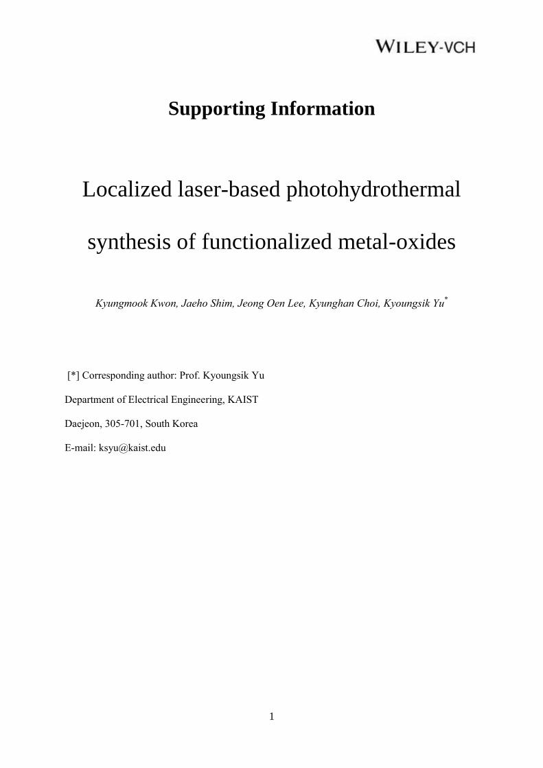
Figure S1. In the conventional large-area bulk heating, it is hard to exceed the boiling point
under the normal ambient pressure. However, PLIH can easily achieve the superheating
condition while preventing explosive bubble generation. (a) Under continuous heating, the
vapor layer continuously grows up, and the excessive vapor pressure results in explosive
bubble generation. (b) With PLIH, the vapor layer collapses during the cooling cycle.
3
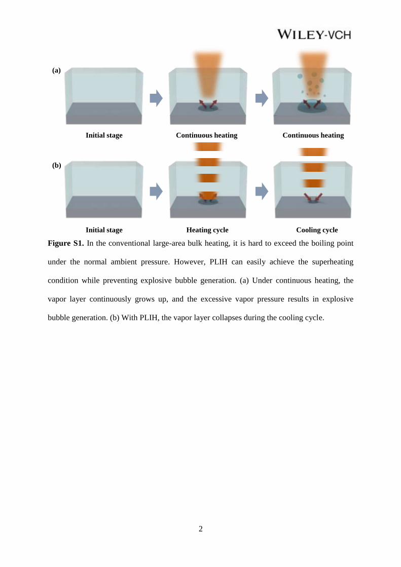
Figure S2. A schematic diagram of the experimental setup for the localized
photohydrothermal synthesis of metal oxide materials with focused laser beam irradiation.
4
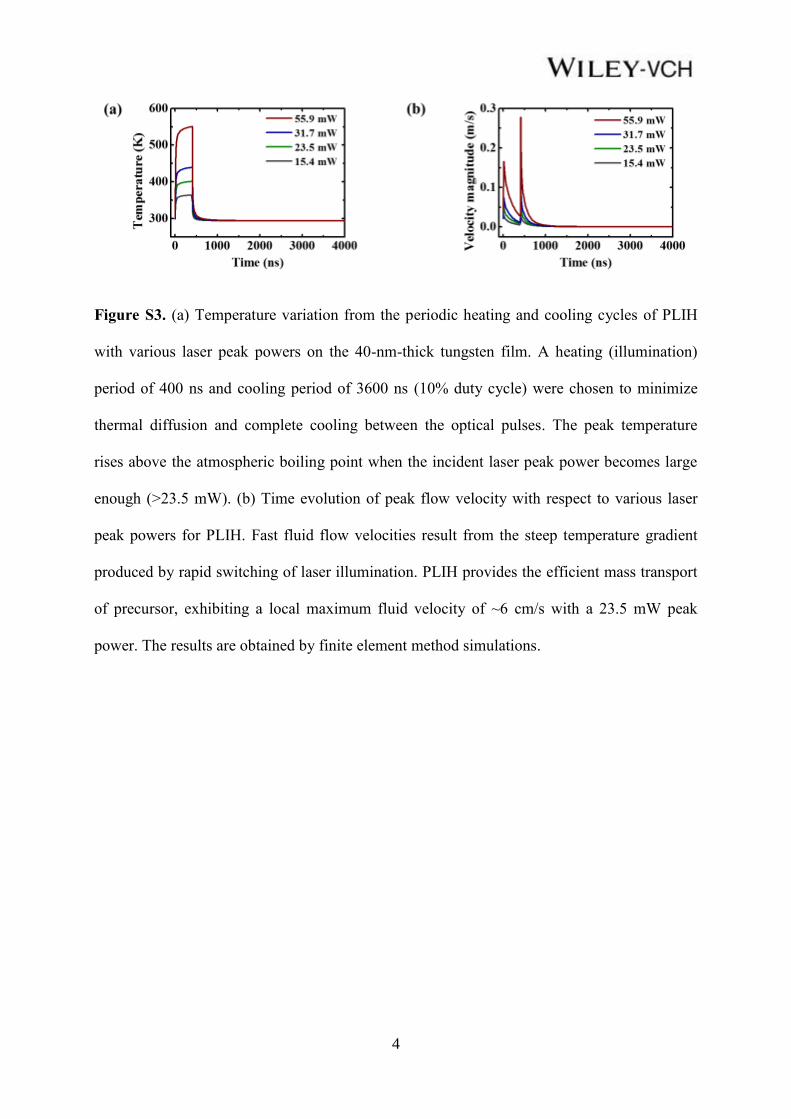
Figure S3. (a) Temperature variation from the periodic heating and cooling cycles of PLIH
with various laser peak powers on the 40-nm-thick tungsten film. A heating (illumination)
period of 400 ns and cooling period of 3600 ns (10% duty cycle) were chosen to minimize
thermal diffusion and complete cooling between the optical pulses. The peak temperature
rises above the atmospheric boiling point when the incident laser peak power becomes large
enough (>23.5 mW). (b) Time evolution of peak flow velocity with respect to various laser
peak powers for PLIH. Fast fluid flow velocities result from the steep temperature gradient
produced by rapid switching of laser illumination. PLIH provides the efficient mass transport
of precursor, exhibiting a local maximum fluid velocity of ~6 cm/s with a 23.5 mW peak
power. The results are obtained by finite element method simulations.

5
Figure S4. Flow velocity profile at 10 seconds with continuous-wave laser illumination (23.5
mW). Under the continuous laser irradiation, the fluid velocity is below 1 μm/s which is quite
slow compared to PLIH in Figure S3. The result is obtained by finite element method
simulations.
6
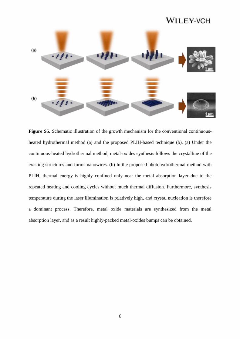
Figure S5. Schematic illustration of the growth mechanism for the conventional continuous-
heated hydrothermal method (a) and the proposed PLIH-based technique (b). (a) Under the
continuous-heated hydrothermal method, metal-oxides synthesis follows the crystalline of the
existing structures and forms nanowires. (b) In the proposed photohydrothermal method with
PLIH, thermal energy is highly confined only near the metal absorption layer due to the
repeated heating and cooling cycles without much thermal diffusion. Furthermore, synthesis
temperature during the laser illumination is relatively high, and crystal nucleation is therefore
a dominant process. Therefore, metal oxide materials are synthesized from the metal
absorption layer, and as a result highly-packed metal-oxides bumps can be obtained.

7
Figure S6. SEM images of zinc oxide bumps photohydrothermally grown on a tungsten film
with various laser peak powers (15.4, 23.5, 31.7, and 55.9 mW) and growth times (0.2, 0.5, 3,
and 10 seconds). All scale bars represent 1 μm.
8
CuO bump Cu O
W Si
(a) (b) (c)
(d) (e)
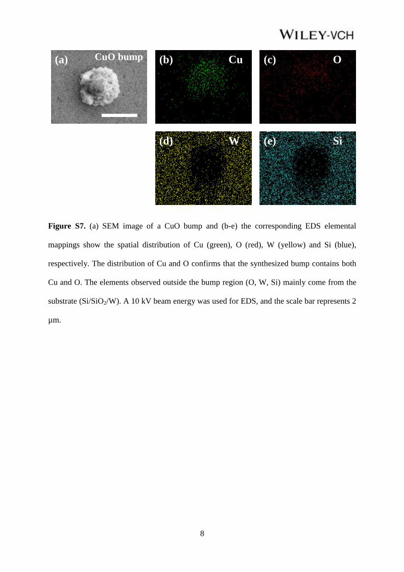
Figure S7. (a) SEM image of a CuO bump and (b-e) the corresponding EDS elemental
mappings show the spatial distribution of Cu (green), O (red), W (yellow) and Si (blue),
respectively. The distribution of Cu and O confirms that the synthesized bump contains both
Cu and O. The elements observed outside the bump region (O, W, Si) mainly come from the
substrate (Si/SiO2/W). A 10 kV beam energy was used for EDS, and the scale bar represents 2
µm.
9
200 400 600 800 1000
Inte
nsi
ty (
a.u
.)
Raman Shift (cm-1
)
Photohydrothermal
CuO bump
(a) (b)
200 400 600 800 1000
Inte
nsi
ty (
a.u
.)
Raman Shift (cm-1
)
Ag
Bg
Bg
TO
Bg
Bg
Ag
Hydrothermal
CuO
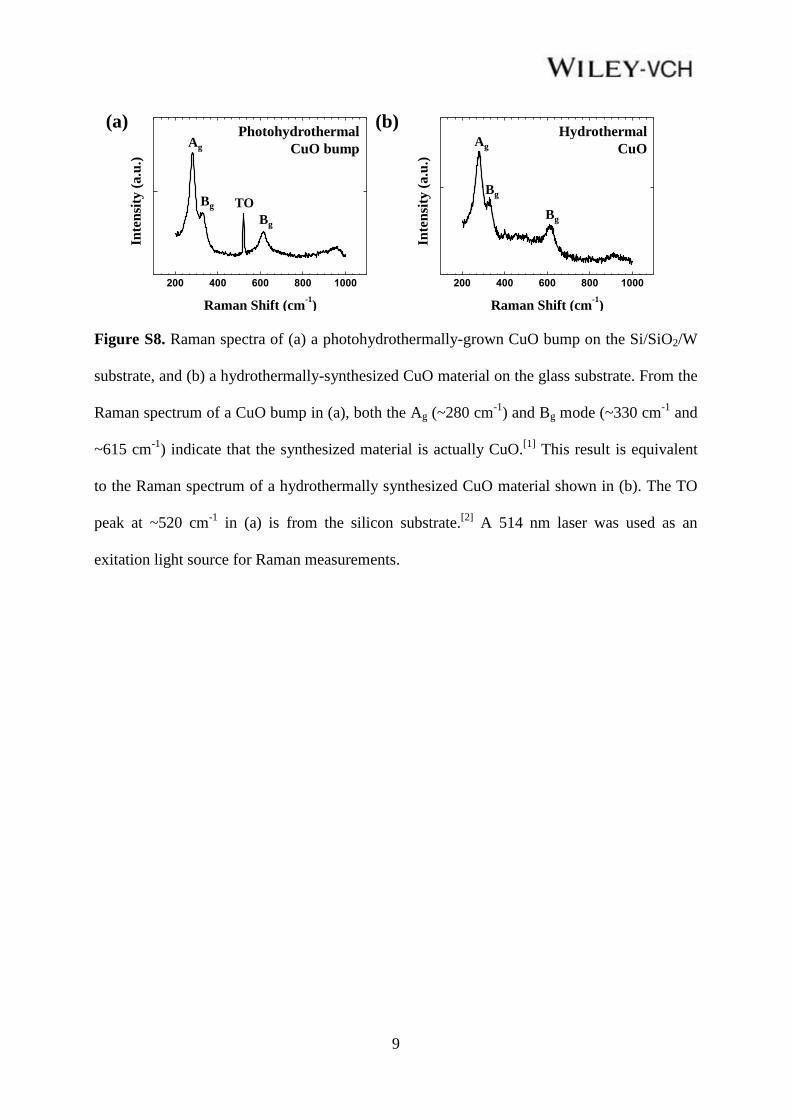
Figure S8. Raman spectra of (a) a photohydrothermally-grown CuO bump on the Si/SiO2/W
substrate, and (b) a hydrothermally-synthesized CuO material on the glass substrate. From the
Raman spectrum of a CuO bump in (a), both the Ag (~280 cm-1
) and Bg mode (~330 cm-1
and
~615 cm-1
) indicate that the synthesized material is actually CuO.[1]
This result is equivalent
to the Raman spectrum of a hydrothermally synthesized CuO material shown in (b). The TO
peak at ~520 cm-1
in (a) is from the silicon substrate.[2]
A 514 nm laser was used as an
exitation light source for Raman measurements.
10
Zn O
W Si
(a) (b) (c)
(d) (e)
ZnO bump
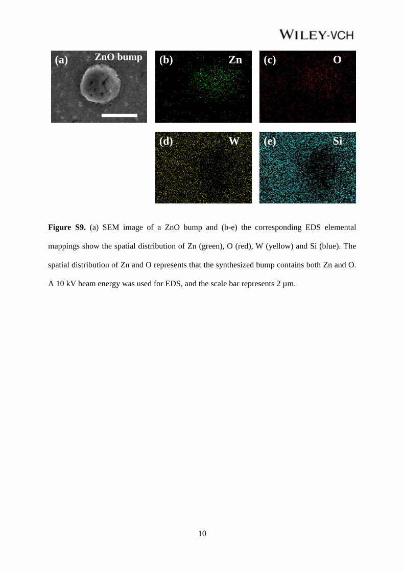
Figure S9. (a) SEM image of a ZnO bump and (b-e) the corresponding EDS elemental
mappings show the spatial distribution of Zn (green), O (red), W (yellow) and Si (blue). The
spatial distribution of Zn and O represents that the synthesized bump contains both Zn and O.
A 10 kV beam energy was used for EDS, and the scale bar represents 2 µm.
11
400 600 800 1000
Inte
nsi
ty (
a.u
.)
Wavelength (nm)
Hydrothermal ZnO
Photohydrothermal
ZnO bump
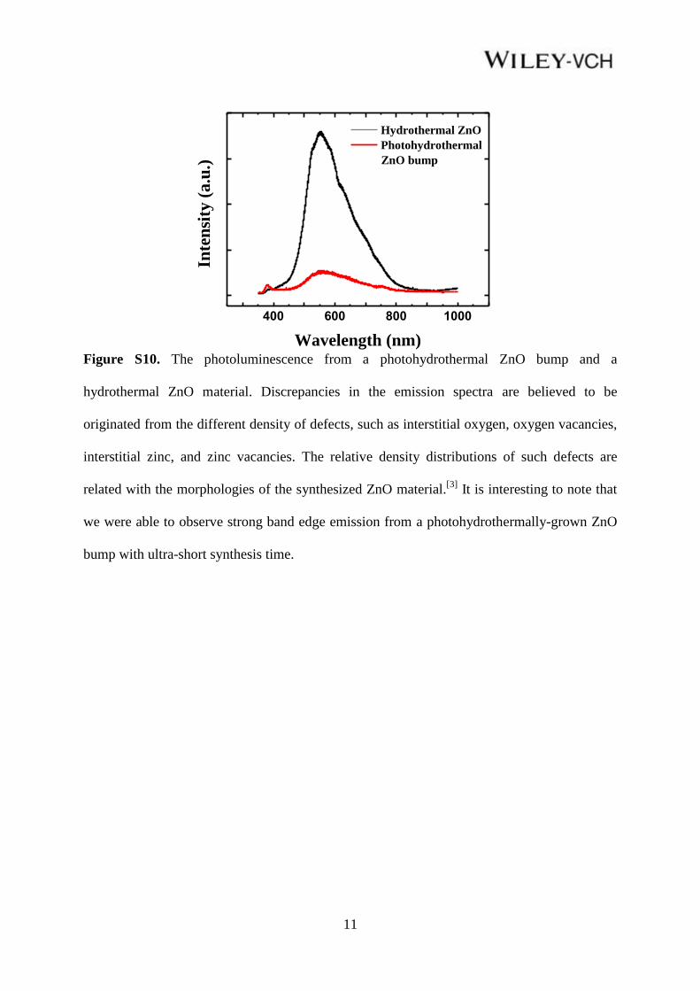
Figure S10. The photoluminescence from a photohydrothermal ZnO bump and a
hydrothermal ZnO material. Discrepancies in the emission spectra are believed to be
originated from the different density of defects, such as interstitial oxygen, oxygen vacancies,
interstitial zinc, and zinc vacancies. The relative density distributions of such defects are
related with the morphologies of the synthesized ZnO material.[3]
It is interesting to note that
we were able to observe strong band edge emission from a photohydrothermally-grown ZnO
bump with ultra-short synthesis time.

12
Figure S11. Voltage distribution profile when 1 V is applied between the top and bottom
tungsten metal strip. The voltage drop mainly occurs at the metal oxide material sandwiched
between the top and bottom electrode.

13
0 1 2 3 4 5
10-10
10-9
10-8
10-7
10-6
10-5
Cu
rren
t (A
)
Voltage (V)
After annealing
As grown
Figure S12. To demonstrate the effect of an additional annealing process, the metal strip lines
electrically connected by a zinc oxide bump was annealed at 260 ℃ for ten hours in the
nitrogen atmosphere. After the annealing process, the conductivity of the zinc oxide solder
bump was significantly enhanced.

14
Reference for Supporting Information
[1] W. Wang, Q. Zhou, X. Fei, Y. He, P. Zhang, G. Zhang, L. Peng, W. Xie,
Crystengcomm 2010, 12, 2232.
[2] E. Quiroga-Gonzalez, J. Carstensen, C. Glynn, C. O'Dwyer, H. Foell, Physical
Chemistry Chemical Physics 2014, 16, 255.
[3] T.-J. Liu, Q. Wang, P. Jiang, Rsc Advances 2013, 3, 12662; A. B. Djurisic, Y. H.
Leung, Small 2006, 2, 944.