
STUDY AND IMPLEMENTA TION OF A PVT INSENSITIVE … · study and implementa tion of a pvt...
78
STUDY AND IMPLEMENTATION OF A PVT INSENSITIVE CMOS OSCILLATOR PEDRO VAZ COKE DISSERTAÇÃO DE MESTRADO APRESENTADA À FACULDADE DE ENGENHARIA DA UNIVERSIDADE DO PORTO EM MESTRADO INTEGRADO EM ENGENHARIA ELECTROTÉCNICA E DE COMPUTADORES M 2014
Transcript of STUDY AND IMPLEMENTA TION OF A PVT INSENSITIVE … · study and implementa tion of a pvt...

STUDY AND IMPLEMENTATION OF A PVT INSENSITIVE CMOS OSCILLATOR
PEDRO VAZ COKE DISSERTAÇÃO DE MESTRADO APRESENTADA À FACULDADE DE ENGENHARIA DA UNIVERSIDADE DO PORTO EM MESTRADO INTEGRADO EM ENGENHARIA ELECTROTÉCNICA E DE COMPUTADORES
M 2014


Study and Implementation of a PVTInsensitive CMOS Oscillator
Pedro Vaz Coke
Disstertation submitted in partial fulfillment of the requirements for the degree ofMaster in Electrical and Computers Engineering
Telecomunications Major
Supervisor: Cândido Duarte (FEUP)
Supervisor: Miguel de Pina (SiliconGate Lda.)
30 June, 2014

c© Pedro Vaz Coke: 30 June, 2014


Abstract
Today virtually every consumer electronics device contains one or more integrated circuits(ICs) that require clock signal generation. This signal must present a certain level of frequencystability even in non-nominal conditions. Ideally, the clock generator block should exhibit a rea-sonably low frequency deviation when subject to process, voltage, and temperature (PVT) varia-tions, such as changes in temperature caused by device heating, low power supply ripple rejectionratio (PSRR), or process parameter fluctuations during the fabrication process.
Typically, clock references are based on crystal oscillators which rely on piezoelectric materi-als to generate precise frequencies. However, with ever decreasing semiconductor process nodesand a growing trend in system integration, the use of external components like crystal referencesincreases size and cost.
The use of simple oscillator topologies so that they can be fully integrated on-chip is possible,but does not provide any compensation in regards to PVT changes. As such, to realize a morereliable oscillator, a compensation scheme must be integrated so that the oscillation frequency canbe stabilized.
The main objective of this work is the CMOS circuit implementation of a PVT insensitiveoscillator suitable for full on-chip integration. A study on the key design considerations for real-ization of PVT insensitive oscillators is also presented. The covered topics include an overview onthe performance of several oscillator topologies implemented in different process nodes, as wellas an analysis of selected compensation circuits.
An alternative methodology for the tuning of the compensation circuits is proposed, compris-ing an automatic optimization algorithm. A novel process compensation circuit is also presented,focusing on the concept of orthogonal PVT compensation.
Finally, a complete implementation of a fully integrated PVT compensated oscillator in adeep-submicron process node is presented. It uses a novel open-loop temperature and processcompensation circuit and comprises a current starved ring oscillator, as well as an on-chip voltagereference.
i


Resumo
Hoje em dia a grande maioria dos dispositivos electrónicos contêm um ou mais circuitos in-tegrados que necessitam de geração de sinais de relógio. Este sinal de relógio deve apresentarum certo nível de estabilidade em frequência, mesmo em condições não típicas. Idealmente, obloco gerador de relógio deverá manter um baixo desvio de frequência quando sujeito a variaçõesde processo, tensão e temperatura (PTT), causadas por aquecimento devido ao calor gerado pelocircuito, baixo rácio de rejeição da tensão de alimentação, ou flutuações no processo de fabrico.
Tipicamente, as referências de relógio usam osciladores de cristal que fazem uso de materiaispiezoeléctricos para gerar frequências precisas. No entanto, com a miniaturização do processode fabrico de semicondutores e a tendência para a integração de sistemas, o uso de componentesexternos como referências de cristal aumenta o tamanho e custo de fabrico.
O uso de topologias de oscilador simples de maneira a que estas sejam implementadas emcircuitos integrados é possível, mas não permite qualquer tipo de compensação em variações dePTT. Como tal, para realizar um oscilador mais robusto, é necessária a integração de um esquemade compensação de maneira a que a frequência de oscilação possa ser estabilizada.
O objectivo do presente trabalho é a implementação de um oscilador insensível a variaçõesPTT que seja passível de ser projectado em circuitos integrados. É também apresentado um estudosobre os pontos chave de projecto deste tipo de osciladores. Os tópicos abordados incluem umavisão geral da performance de várias topologias de osciladores implementados em vários nós deprocesso, assim como uma análise de circuitos de compensação.
Uma metodologia alternativa para ajuste de circuitos de compensação é proposta, com basenum algoritmo de optimização. Mais ainda, é apresentado um novo circuito para compensação devariações de processo, com foco no conceito de compensação PTT ortogonal.
Por último, é também apresentada a implementação completa de um oscilador compensado emPTT totalmente integrado num nó de processo sub-micrométrico. Este faz uso de um novo circuitode compensação em processo e temperatura e é formado por um oscilador em anel alimentado emcorrente, assim como uma referência de tensão integrada.
iii


Acknowledgments
To my mother for her unconditional support, and to my girlfriend for motivating me still tomove forward.
To my good friend and supervisor Cândido Duarte, who first introduced me to integrated cir-cuit design, and without whom this dissertation would not have been possible.
To Miguel de Pina, Daniel Oliveira, and Américo Dias, for their outstanding moral and tech-nical support, as well as their talent for creating a highly motivating work environment.
Lastly, to the faculty Microelectronics Students’ Group and to SiliconGate Lda. for providingall the required work infrastructure.
Pedro Vaz Coke
v


“It’s a machine”
Miguel de Pina
vii


Contents
List of Figures xii
List of Tables xiii
List of Abbreviations xv
1 Introduction 11.1 Temperature effects . . . . . . . . . . . . . . . . . . . . . . . . . . . . . . . . . 11.2 Process variations . . . . . . . . . . . . . . . . . . . . . . . . . . . . . . . . . . 2
1.2.1 Statistical models . . . . . . . . . . . . . . . . . . . . . . . . . . . . . . 21.3 Design for variability . . . . . . . . . . . . . . . . . . . . . . . . . . . . . . . . 31.4 Problem statement . . . . . . . . . . . . . . . . . . . . . . . . . . . . . . . . . 51.5 Proposed approach . . . . . . . . . . . . . . . . . . . . . . . . . . . . . . . . . 51.6 Document structure . . . . . . . . . . . . . . . . . . . . . . . . . . . . . . . . . 6
2 Literature Review 72.1 Analog open-loop compensation . . . . . . . . . . . . . . . . . . . . . . . . . . 82.2 Closed-loop approach . . . . . . . . . . . . . . . . . . . . . . . . . . . . . . . . 11
2.2.1 Comparator loop . . . . . . . . . . . . . . . . . . . . . . . . . . . . . . 112.2.2 Switched capacitor loop . . . . . . . . . . . . . . . . . . . . . . . . . . 142.2.3 SAR loop . . . . . . . . . . . . . . . . . . . . . . . . . . . . . . . . . . 152.2.4 Frequency-locked loop . . . . . . . . . . . . . . . . . . . . . . . . . . . 17
2.3 Other techniques . . . . . . . . . . . . . . . . . . . . . . . . . . . . . . . . . . 182.3.1 Structural approaches . . . . . . . . . . . . . . . . . . . . . . . . . . . . 182.3.2 Reference modeling . . . . . . . . . . . . . . . . . . . . . . . . . . . . 19
2.4 Overview . . . . . . . . . . . . . . . . . . . . . . . . . . . . . . . . . . . . . . 19
3 Analysis on Oscillator Performance 213.1 Current starved ring oscillator . . . . . . . . . . . . . . . . . . . . . . . . . . . 213.2 Differential delay cell ring oscillator . . . . . . . . . . . . . . . . . . . . . . . . 243.3 High-performance VCO . . . . . . . . . . . . . . . . . . . . . . . . . . . . . . 263.4 Relaxation oscillator . . . . . . . . . . . . . . . . . . . . . . . . . . . . . . . . 283.5 Results overview . . . . . . . . . . . . . . . . . . . . . . . . . . . . . . . . . . 33
4 Compensation Circuits 354.1 Conventional compensation . . . . . . . . . . . . . . . . . . . . . . . . . . . . . 364.2 Quasi-orthogonal compensation . . . . . . . . . . . . . . . . . . . . . . . . . . 404.3 Results overview . . . . . . . . . . . . . . . . . . . . . . . . . . . . . . . . . . 42
ix

x CONTENTS
5 Implementation 455.1 Bandgap voltage reference . . . . . . . . . . . . . . . . . . . . . . . . . . . . . 455.2 Temperature and process compensation . . . . . . . . . . . . . . . . . . . . . . 475.3 Oscillator and output stage . . . . . . . . . . . . . . . . . . . . . . . . . . . . . 485.4 Results . . . . . . . . . . . . . . . . . . . . . . . . . . . . . . . . . . . . . . . . 48
6 Conclusions and Future Work 516.1 Future work . . . . . . . . . . . . . . . . . . . . . . . . . . . . . . . . . . . . . 51
References 53

List of Figures
1.1 Circuit for process sensing in NMOS and PMOS versions . . . . . . . . . . . . . 31.2 Output of the NMOS and PMOS process sensor over sensor transistor length and
process corners . . . . . . . . . . . . . . . . . . . . . . . . . . . . . . . . . . . 4
2.1 Block diagram of typical open-loop compensation topology . . . . . . . . . . . . 82.2 Circuits for TPC proposed by Shyu et al. and Sundaresan et al. . . . . . . . . . . 92.3 Replica biasing circuit proposed by Maneatis et al. . . . . . . . . . . . . . . . . 102.4 System diagram of the comparator-based compensation loop . . . . . . . . . . . 122.5 Frequency sensor implementation and control signals as proposed by Zhang et al. 122.6 Linear continuous-time model of the comparator-based compensation loop . . . . 132.7 System diagram of the capacitor-based compensation loop proposed . . . . . . . 142.8 Switched capacitor implementation of the frequency correction block and control
signals . . . . . . . . . . . . . . . . . . . . . . . . . . . . . . . . . . . . . . . . 152.9 System diagram of the SAR compensation loop . . . . . . . . . . . . . . . . . . 162.10 System diagram of the FLL compensation loop . . . . . . . . . . . . . . . . . . 172.11 Schematic of the addition-based RO . . . . . . . . . . . . . . . . . . . . . . . . 182.12 Schematic of the addition-based current-source . . . . . . . . . . . . . . . . . . 19
3.1 Schematic of the current starved RO . . . . . . . . . . . . . . . . . . . . . . . . 223.2 Simulation results of the current starved RO output waveform . . . . . . . . . . . 223.3 Simulation results for frequency deviation of the current starved RO over process
and temperature corners . . . . . . . . . . . . . . . . . . . . . . . . . . . . . . . 233.4 Schematic of the differential delay cell RO . . . . . . . . . . . . . . . . . . . . . 243.5 Schematic of the differential delay cell . . . . . . . . . . . . . . . . . . . . . . . 243.6 Schematic of the replica bias generator . . . . . . . . . . . . . . . . . . . . . . . 253.7 Simulation results of the differential delay cell RO output waveform . . . . . . . 253.8 Simulation results for frequency deviation of the differential delay cell RO over
process and temperature corners . . . . . . . . . . . . . . . . . . . . . . . . . . 263.9 Schematic of the high-performance VCO . . . . . . . . . . . . . . . . . . . . . 273.10 Simulation results of the high-performance VCO output waveform . . . . . . . . 273.11 Simulation results for frequency deviation of the high-performance VCO over pro-
cess and temperature corners . . . . . . . . . . . . . . . . . . . . . . . . . . . . 283.12 Schematic of the relaxation oscillator . . . . . . . . . . . . . . . . . . . . . . . . 293.13 Schematic of the two-stage comparator . . . . . . . . . . . . . . . . . . . . . . . 303.14 Schematic of the modified two-stage comparator for low VREF operation . . . . . 303.15 Comparator output behaviour at low VREF operation with and without the added
reset circuit . . . . . . . . . . . . . . . . . . . . . . . . . . . . . . . . . . . . . 313.16 Simulation results of the relaxation oscillator output waveform . . . . . . . . . . 32
xi

xii LIST OF FIGURES
3.17 Simulation results for frequency deviation of the relaxation oscillator over processand temperature corners . . . . . . . . . . . . . . . . . . . . . . . . . . . . . . . 32
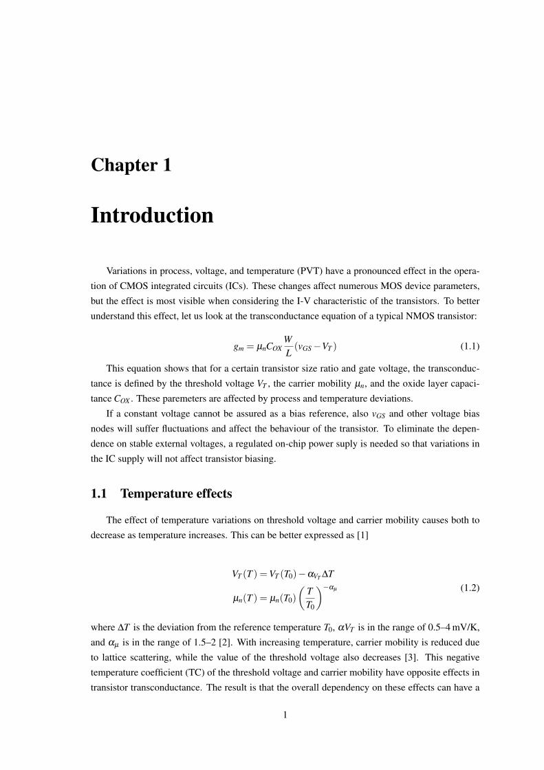
4.1 Schematic of the conventional compensation circuit . . . . . . . . . . . . . . . . 364.2 Representation of the bi-dimensional algorithm sweep space . . . . . . . . . . . 374.3 Optimization algorithm flow chart . . . . . . . . . . . . . . . . . . . . . . . . . 384.4 Simulation results of the current starved and differential delay cell ROs compen-
sated by the conventional circuit across MOS, resistor and bipolar process corners 394.5 Schematic of an ideal vt sensor, and the quasi-orthogonal compensation circuit . . 404.6 Simulation results of the current starved and differential delay cell ROs compen-
sated by the quasi-orthogonal circuit across MOS process corners . . . . . . . . 42
5.1 Block diagram of the implemented PVT insensitive oscillator . . . . . . . . . . . 455.2 Schematic of the bandgap voltage reference . . . . . . . . . . . . . . . . . . . . 465.3 Schematic of the operational amplifier . . . . . . . . . . . . . . . . . . . . . . . 465.4 Simulation results of the bandgap output voltage VREF across supply and MOS,
resistor and bipolar process corners . . . . . . . . . . . . . . . . . . . . . . . . . 475.5 Schematic of TPC circuit . . . . . . . . . . . . . . . . . . . . . . . . . . . . . . 475.6 Schematic of oscillator block and output buffer circuits . . . . . . . . . . . . . . 485.7 Simulation results of the compensated oscillator across MOS, resistor and bipolar
process corners . . . . . . . . . . . . . . . . . . . . . . . . . . . . . . . . . . . 495.8 Simulation results of output waveform of the compensated oscillator . . . . . . . 49

List of Tables
1.1 Intra-die variability of threshold voltage in CMOS technology nodes . . . . . . . 2
2.1 Comparison of analog open-loop implementations . . . . . . . . . . . . . . . . . 112.2 Comparison of closed-loop implementations . . . . . . . . . . . . . . . . . . . . 172.3 Comparison of PVT compensated oscillators . . . . . . . . . . . . . . . . . . . . 20
3.1 Performance of the current starved RO for various processes . . . . . . . . . . . 233.2 Performance of the differential delay cell RO for various processes . . . . . . . . 263.3 Performance of the high-performance VCO for various processes . . . . . . . . . 283.4 Performance of the relaxation oscillator for various processes . . . . . . . . . . . 32
4.1 Performance of the current starved and differential delay cell ROs with and with-out conventional compensation . . . . . . . . . . . . . . . . . . . . . . . . . . . 38
4.2 Performance of the current starved and differential delay cell ROs with and with-out quasi-orthogonal compensation . . . . . . . . . . . . . . . . . . . . . . . . . 41
5.1 Comparison of open-loop PVT compensated oscillators . . . . . . . . . . . . . . 49
xiii


List of Abbreviations
ADC Analog-to-Digtal Converter
CP Charge Pump
CTAT Complementary To Absolute Temperature
DAC Digtal-to-Analog Converter
EDA Electronic Design Automation
FLL Frequency-Locked Loop
IC Integrated Circuit
LCO LC Oscillator
LPF Low-Pass Filter
NVM Non-Volatile Memory
PDK Process Design Kit
PLL Phase-Locked Loop
PSRR Power Supply Ripple Rejection Ratio
PTAT Proportional To Absolute Temperature
PVT Process, Voltage, and Temperature
RO Ring Oscillator
SAR Successive Approximation Register
TC Temperature Coefficient
TPC Temperature and Process Compensation
VCO Voltage Controlled Oscillator
xv

Chapter 1
Introduction
Variations in process, voltage, and temperature (PVT) have a pronounced effect in the opera-
tion of CMOS integrated circuits (ICs). These changes affect numerous MOS device parameters,
but the effect is most visible when considering the I-V characteristic of the transistors. To better
understand this effect, let us look at the transconductance equation of a typical NMOS transistor:
gm = µnCOXWL(vGS−VT ) (1.1)
This equation shows that for a certain transistor size ratio and gate voltage, the transconduc-
tance is defined by the threshold voltage VT , the carrier mobility µn, and the oxide layer capaci-
tance COX . These paremeters are affected by process and temperature deviations.
If a constant voltage cannot be assured as a bias reference, also vGS and other voltage bias
nodes will suffer fluctuations and affect the behaviour of the transistor. To eliminate the depen-
dence on stable external voltages, a regulated on-chip power suply is needed so that variations in
the IC supply will not affect transistor biasing.
1.1 Temperature effects
The effect of temperature variations on threshold voltage and carrier mobility causes both to
decrease as temperature increases. This can be better expressed as [1]
VT (T ) =VT (T0)−αVT ∆T
µn(T ) = µn(T0)
(TT0
)−αµ (1.2)
where ∆T is the deviation from the reference temperature T0, αVT is in the range of 0.5–4 mV/K,
and αµ is in the range of 1.5–2 [2]. With increasing temperature, carrier mobility is reduced due
to lattice scattering, while the value of the threshold voltage also decreases [3]. This negative
temperature coefficient (TC) of the threshold voltage and carrier mobility have opposite effects in
transistor transconductance. The result is that the overall dependency on these effects can have a
1

2 Introduction
non-monotonic relation with temperature [4]. In certain conditions, the output may be the same
for some different temperatures. This relation has been exploited to realize temperature-stable
circuits such as voltage references [5].
1.2 Process variations
The IC fabrication process also leads to variations that have a strong impact in circuit be-
haviour. Differences in doping levels alter carrier mobility and changes in gate dielectric thick-
ness affect threshold voltages and oxide layer capacitance. Moreover, as semiconductor fabrication
technology advances into deep-submicron CMOS process nodes, the magnitude of variability in-
creases. At smaller scales, single dopant atoms and small fluctuations in local oxide thickness can
have significant effects in device performance [6]. In fact, the intra-die threshold voltage variabil-
ity increases in an almost inversely proportional manner, relative to process node size, as shown
in table 1.1 [7].
Table 1.1: Intra-die variability of threshold voltage in CMOS technology nodes [7].
Process node 250 nm 180 nm 130 nm 90 nm 65 nm 45 nmσVT /VT 4.7% 5.8% 8.2% 9.3% 10.7% 16%
1.2.1 Statistical models
Modelling of these variations so that they can be taken into account during the design process
relies on electronic design automation (EDA) software, and can cover inter-die or intra-die varia-
tions. The case of inter-die variation modeling estimates that all devices in the IC die will suffer
the same fluctuations. For this scenario there exist two types of simulation models: statistical
analysis models for Monte Carlo simulations and absolute corners. The statistical analysis mod-
els contain typical distribution functions for process parameters, provided by the foundry. These
models allow running large amounts of single simulations where these parameters are selected at
random from the distribution functions. They are particularly useful for fabrication yield estima-
tion in large production circuits. A typical target in IC design is to achieve 3-sigma yields, where
the device passes specifications in 99.7% of the Monte Carlo simulations (a 6-sigma target may
be used for high-yield designs).
The absolute corner process models are simpler to use in terms of computation time and simu-
lation setup, and approach the issue of process variability modeling from a worst case perspective.
They are derived from the distribution functions used in the previously mentioned statistical mod-
els, where the corners (maximum and minimum) for each process parameter are taken from a 3 or
6-sigma variation. As such, a circuit design which is within specification in all process corners,
could be estimated to produce > 99% yield. Typically corners are provided for MOS devices,
as well as passive and other types of active devices such as diodes and bipolar transistors. For
MOS devices, the model includes corners for fast and slow cases of NMOS and PMOS variations,

1.3 Design for variability 3
resulting in four corners: fastN-fastP (FF), fastN-slowP (FS), slowN-fastP (SF) and slowN-slowP
(SS). The slow process corners are a consequence of reduced carrier mobility and thicker gate
dielectric, which lowers the oxide layer capacitance and increases the threshold voltage, with the
fast corner experiencing opposite effects. These variations result in a lower (higher for the fast
corner) drain current for the same bias voltage, hence the “slow” and “fast” nomenclature. For the
rest of the device types there typically exist minimum and maximum corners to model the worst
case variations.
For intra-die variation modeling, random variation are taken from a set of process parameter
distribution functions, for each device in the design. For this reason, they are also known as mis-
match models. Such models become more useful for large IC designs, where the assumption that
all devices will suffer the same process variations is no longer reasonable, due to the large die area.
For small designs, however, the use of yield targets with mismatch models may lead to unreason-
able overdesign. Moreover, for some circuits, critical constructs where matching is important may
be easily identified, and taken into account during layout design such that the effect of device mis-
match is minimized. Examples of such cases are MOS current mirrors, resistor pairs or capacitor
arrays, where layout techniques such as interdigitation and common centroid can greatly increase
matching and reduce the effect of intra-die process variations. In sum, although mismatch models
are needed for large area or high-yield designs, for small designs where good layout techniques for
device matching are employed, their use might be unnecessary or even detrimental to the design
process.
1.3 Design for variability
In deep-submicron nodes, variability not only increases in magnitude, as mentioned earlier,
but is also highly process-dependent. This further increases the need for foundry process variation
models to validate IC designs. It also increases the complexity of designing and realizing PVT-
insensitive circuits, which falls in the scope of this work.
VbiasP
VsenseN
(a)
VsenseP
VbiasN
(b)
Figure 1.1: Circuit for process sensing in (a) NMOS and (b) PMOS versions.
As a basic example of process variability, let us consider a classic example of a threshold volt-
age sensor used for process compensation [8]. The circuit is shown in Fig. 1.1, in both PMOS and

4 Introduction
NMOS versions. It comprises a diode connected MOS device, which acts as the process sensor,
and a complementary transistor acting as a current source, with a fixed bias voltage applied at
the gate. The output voltage is at the drain of the process sensor device, and varies according to
process deviations. To illustrate the sensitivity to device sizing and process corner interaction be-
tween devices, the circuit was implemented in a 90 nm process and simulated for different process
sensor gate lengths, while the current source MOS device was kept at constant size.
V sen
seN
(V)
Length (µm)
SNFPFFTTSS
FNSP
0.5
0.6
0.7
0.8
0.9
1
1.1
2 4 6 8 10 12 14 16 18 20
(a)
V sen
seP
(V)
Length (µm)
SNFPFFTTSS
FNSP
0.2
0.4
0.6
0.8
1
1.2
1.4
1.6
2 4 6 8 10 12 14 16 18 20
(b)
Figure 1.2: Output of the (a) NMOS and (b) PMOS process sensor over sensor transistor lengthand process corners.
The simulation results are shown in Fig. 1.2. The net result from process variations is the
circuit becoming more sensitive to mismatched PMOS and NMOS process variations (FS and SF
corners). Also note that depending on the process sensor size, the FF and SS corners change
order. Not shown is the variation in the TC, which changes from negative to positive as the NMOS
process sensor length increases, while the PMOS version exhibits the opposite behaviour.
The purpose of this example is to show how device sizing and interaction in a circuit may result
in unexpected behaviour over process and temperature variations. As circuit complexity increases,

1.4 Problem statement 5
it can become difficult to predict the result over corners. The use of analytical expressions for
such a task is non-trivial due to the complexity of the process parameters that must be taken into
account, and falls outside the scope of this work.
1.4 Problem statement
Today virtually every consumer device contains one or more ICs comprising some type of
circuitry that requires a clock signal. As such, clock generation is a required component on almost
any electronic system.
For many electronic circuits, the clock signal must also present a certain level of stability even
in non-nominal conditions. Ideally, the clock generator block should exhibit a reasonably low
frequency deviation when subject to PVT variations. Changes in temperature and voltage occur
over time, and can be caused by internal factors such as heat generated by the device or low power
supply ripple rejection ratio (PSRR), or external such to environmental changes or electrical noise.
In contrast, changes in process are by nature static and permanent for each device, as they occur
due to parameter deviations during the fabrication process.
Typically, clock references are based on crystal oscillators. They rely on piezoelectric mate-
rials to generate precise frequencies, and provide good stability over temperature. However, with
ever decreasing semiconductor process nodes and a growing trend in system integration, the use
of external components like crystal references increases size and cost.
The use of simple oscillator topologies, so that they can be fully integrated on-chip, is possible,
but does not provide any compensation in regards to PVT changes. As such, to realize a more
reliable oscillator, a compensation scheme must be integrated so that the oscillation frequency can
be stabilized.
1.5 Proposed approach
This works aims to cover the key design considerations for the realization of PVT insensi-
tive oscillators, as well as to propose new methodologies and circuit implementations. Due to the
unpredictable nature of process variations, analytical analysis is of limited use, and instead a prac-
tical approach is taken. The focus is on providing straightforward design flows and simple circuit
realization methodologies through the use of orthogonal compensation mechanisms for process,
voltage, and temperature variations.
In regards to the use of EDA software, the Cadence Virtuoso design suite was used for circuit
schematic capture, Synopsys HSPICE and WaveView for circuit simulation and results visualiza-
tion, and Mathworks MATLAB for additional numeric processing of results and implementation of
optimization algorithms.

6 Introduction
1.6 Document structure
The document structure consists of a literature review, and analysis on the performance of
oscillators, analysis of compensation circuits, description of the proposed implementation and
finally conclusions and future work.
In chapter 2, a brief review of the existing literature on PVT insensitive oscillators is presented,
providing an overview of the state of the art.
Chapter 3 covers a selected set of oscillator topologies to provide a brief circuit study and
general comparison on key performance metrics.
On chapter 4, the focus shifts to compensation circuits, where new approaches to design flow
are proposed and tested.
The implementation of this new compensation circuit is described in chapter 5, and the ob-
tained results are presented.
Lastly, chapter 6 provides the insights and conclusions that arise from the development of this
work, as well as stating future work on the topic.

Chapter 2
Literature Review
In this chapter a brief review of current literature on design techniques for PVT insensitive
oscillators is presented. Most PVT insensitive oscillator designs are comprised of two main blocks,
an oscillator block and a compensation circuit. The oscillator is responsible for synthesizing the
output signal, however it is sensitive to PVT variations and must be able to be tuned in order to
compensate for frequency deviations. As such, this block is usually a voltage controlled oscillator
(VCO), and in most systems it is based on a ring oscillator (RO) architecture, since it is relatively
simple to realize without large area and power requirements. However, implementations using
other oscillator topologies, such as LC or relaxation, also exist.
The compensation block must sense in some way any deviations from the nominal frequency,
and tune the VCO in order to correct them. In sections 2.1 and 2.2 the two most relevant compen-
sation methods are described, analog open-loop and closed loop. The former relies on an analog
compensation block that corrects for temperature and process variations. This process is essen-
tially a form of pre-distortion. Whereas in an ideal circuit the VCO voltage would be kept to
generate a constant frequency, analog open-loop compensation generates a process and tempera-
ture dependent control voltage that opposes the VCO variation. This control voltage is specific
to the VCO used, and must also be tuned for the PVT behaviour of the process node used in the
design.
Conversely, closed-loop compensation schemes employ a more generic approach, which can
be applied to any generic VCO block. The control voltage correction is performed by sensing the
output frequency, comparing it with a reference, and minimizing the error. This compensation
block can be implemented in different ways, from a full analog comparator-based scheme, to a
digital successive approximation register (SAR)-based approach.
The last section covers other selected PVT compensation techniques, which are included to
provide a complete overview of the state of the art.
Throughout the analysis of relevant literature, it is evident that the challenge in designing PVT
insensitive oscillators lies mostly in process and temperature compensation. The realization of
PVT insensitive voltage references is a well-understood topic and many works in this area exist,
e.g. bandgap references [9, 10], used in some of the compensation methods found in literature.
7

8 Literature Review
2.1 Analog open-loop compensation
bandgapreference
temperature/process
compensationreplica
feedback bias
VDD
VREF
VBP
VBN
VCT RLcomparatoroscillator
Vout
Figure 2.1: Block diagram of typical open-loop compensation topology.
Design of PVT insensitive oscillators employing analog open-loop compensation methods rely
on process and temperature-sensitive bias circuits to control the oscillator frequency. These com-
pensation schemes follow a similar topology as shown in Fig. 2.1, which comprises the following
blocks:
• Bandgap reference which provides a reference voltage VREF , independent of temperature,
process, and supply variations. This is used as a supply voltage for all the circuits up until,
and including, the oscillator block, to reduce system variations due to voltage sensitivity.
• A temperature and process compensation (TPC) circuit that senses changes in these quan-
tities and generates a proportional output voltage VCT RL, similar to pre-distortion methods.
This voltage is used to control the oscillator and thus the TPC block is ultimately responsible
for making the system insensitive to temperature and process variations.
• The replica biasing circuit generates the oscillator bias voltages VBN and VBP from VCT RL.
This block uses self-biasing techniques to generate stable voltages.
• The oscillator block synthesizes the reference frequency, which will depend on the bias
voltage applied by the replica feedback circuit. A buffer is used at the block output to
saturate the signal to VREF . In relevant literature a RO is commonly used.
• A comparator is used to buffer the output signal and saturate it to VDD.
Due to the open-loop nature of the system, the TPC should be tuned so that the control voltage
closely matches the oscillator deviations due to process and temperature changes. Assuming we
define a reasonable working temperature and voltage range, there should exist a bias voltage that
keeps the oscillator at the target nominal frequency across the PVT corners. Once the variation of
this optimal bias voltage across the desired corners is obtained, the TPC circuit should be tuned to
match it. Depending on the TPC block design, several circuit parameters may be used for tuning
the control voltage. These tuning points result in varying degrees of freedom when adjusting the

2.1 Analog open-loop compensation 9
temperature and process slopes to achieve ideal compensation throughout all corners. This tuning
procedure is done via circuit simulation, using process variation corner models.
M1
M2
VCT RL
R1I
Q1
(a)
M3
M1
R1
Q1
M4
M2
R2
Q2
M5
M8 M7
M6
VREF
−
+
R3
R4
VtREF
M9
VCT RL
R5I
Q3
(b)
Figure 2.2: Circuits for TPC proposed by (a) Shyu et al. [8] and (b) Sundaresan et al. [11].
The TPC circuits typically comprise two sections, where different elements are responsible for
sensing temperature and process variations. One of the first such circuits is proposed in [8] and is
shown in Fig. 2.2(a). The diode-connected MOS transistor M2 is used as a threshold voltage VT
sensitive element. Temperature sensing is done via the vEB of the diode-connected PNP transistor
Q1 that exhibits a negative temperature coefficient. The resistor R1 and Q1 can be seen as a

10 Literature Review
temperature-dependent current source, and the output voltage VCT RL is given by
VCT RL =VDD−2|VT |−
√I
K(W/L)2(2.1)
This compensation circuit is used in [8] with RO-based VCO and implemented in a 0.6 µm process,
achieving a 680 kHz output frequency with 4.7% measured accuracy.
The circuit in Fig. 2.2(b), proposed by Sundaresan et al., uses a similar Vt sensor, relying on
a more robust reference current source. This first stage generates a process-dependent buffered
signal VtREF , which is also temperature independent, limited by the matching of the resistors. The
second stage, closely resembles the previous TPC circuit, and as such senses both temperature and
process changes. Similarly to (2.1), the output VCT RL is given by [11]
VCT RL =VtREF −|VT 9|−
√I
K(W/L)9(2.2)
It depends on both the process-dependent voltage VtREF , but also on the threshold voltage of
M9. This is done since the size of M9, along with the value of R5, can used as an additional degree
of freedom for tuning the process and temperature slopes of the TPC circuit.
An enhanced version of this circuit is also proposed by Sundaresan et al., which includes ad-
ditional elements to provide more tuning points. This version is implemented in [11] in a 0.25 µm
process, and is able to achieve 1.29% and 0.84% measured process and temperature variations,
respectively, with a 7 MHz nominal output frequency.
Other works opt to reduce the overall complexity of the TPC circuit, using a bandgap voltage
reference as a proportional to absolute temperature (PTAT) current source [12]. In [13], a leakage
current sensor [14] is used as a process sensor, but on the other hand, a 2-bit DAC is required to
generate the control voltage.
M4
VREF
M3
VCT RL
M2
M1
M5
M6
VBP
M7
M8
VREF
VBN−
+
Figure 2.3: Replica biasing circuit proposed in [15].
The control voltage generated by the TPC block is fed to a replica biasing circuit [15] that
drives the RO, as shown in Fig. 2.3. The bias generator produces the bias voltage VBN from VCT RL,

2.2 Closed-loop approach 11
using a half-buffer replica. An additional half-buffer replica is used to generate VBP, which tracks
VCT RL, but is isolated to prevent potential capacitive coupling.
The premise of this method is that the control voltages generated by the TPC block will com-
pensate the oscillator deviations due to process and temperature variations. One must ensure the
TPC block is accurately tuned, since any error directly compromises the frequency accuracy of the
system across PVT corners. Due to the fact that the control voltage must be tuned to match the os-
cillator behaviour, the design and implementation of this topology must target a specific oscillator
type and fabrication process. This compromises the portability of this compensation method, since
changes in the oscillator or migration to a different process will require re-tuning the TPC block,
which in the worst case can imply a re-design effort. Moreover, since it is infeasible to measure the
oscillator block behaviour from fabricated CMOS samples due to cost and time restrictions, one
must typically rely on simulation results to tune the TPC circuit. As such, one must ensure that
the foundry-provided process design kit (PDK) contains device models that allow process corner
and statistical analysis with acceptable accuracy.
Table 2.1: Comparison of analog open-loop implementations.
Ref Process Frequency Area Power (mW) Accuracy (%)[8] 0.6 µm 680 kHz 0.075 mm2 0.4 4.7[11] 0.25 µm 7 MHz 1.6 mm2 1.5 2.64[12] 0.18 µm 150 MHz Simulation 0.537 2.29[13] 0.18 µm 2 MHz 0.045 µm2 0.048 2.81[16] 0.18 µm 20 MHz N/A N/A 2.98
This open-loop topology has been used to realize oscillators in the range of 640 kHz to 150 MHz
[8,11–13,16], with a frequency sensitivity that is typically around 3%. A brief comparison of rel-
evant works in literature is shown in table 2.1.
2.2 Closed-loop approach
Closed-loop topologies aim to minimize the error between the output clock and a stable, on-
chip reference, through a feedback loop. In this approach, the compensation blocks in the feedback
path are designed to be insensitive to PVT variations in order to reliably measure and minimize
the error of the blocks that are not.
Unlike open-loop methods where the control voltage is generated to compensate a well-known
oscillator behaviour over process and temperature corners, in closed-loop methods the compensa-
tion circuit senses the output frequency and acts on the VCO accordingly in order to correct for
deviations.
2.2.1 Comparator loop
Comparator-based loops have a similar working principle as typical phase-locked loop (PLL)
architectures (Fig. 2.4), where the phase-frequency detector is replaced by a frequency sensor that

12 Literature Review
outputs a DC signal which is compared to a stable voltage reference.
The frequency sensor in Fig. 2.5 uses a capacitance to integrate a reference current, which is
then discharged to a second capacitor to obtain a DC voltage VFS proportional to the oscillator
frequency. In order to minimize the switching frequency, a timing block uses the output clock
signal to generate the (4 times slower) control signals that drive the frequency sensor switches.
frequencysensor
generatortiming
IREF
C
CP/LPF
comparator
VCO
Vout
VCT RL
VREF
VFS
Figure 2.4: System diagram of the comparator-based compensation loop.
The output of the frequency sensor VFS is then compared to a reference voltage in order to de-
termine if the oscillator is operating at the desired frequency. The voltage VFS is fed into a pair of
comparators that decide if it is above or below a reference VREF , which defines the nominal oscil-
lator frequency. The comparator can be realized with simple differential amplifier, with emphasis
on reducing its offset voltage.
A charge pump (CP) and low-pass filter (LPF), controlled by the comparator outputs adjusts
the oscillator control voltage to eventually compensate for process and temperature variations.
When VFS approaches VREF , the comparator falls into the transition region. As such, the charge
pump "up" and "down" currents, IUP and IDN , should match also when the comparator output is at
VDD/2.
RST
CLK
IREF
VP
CFS
SPVFS
CFS
(a)
NToscCLK
SP
RST
VP
VFS
(b)
Figure 2.5: (a) Frequency sensor as proposed in [17], and (b) control signals.

2.2 Closed-loop approach 13
The relative frequency accuracy of the compensation loop is defined by [17]
(σ f
f 0osc
)2
=
(σT
T 0osc
)2
≈(
σI
I0REF
)2
+
(σC
C0FS
)2
+σ2
REF +σ2CP,o f f +
σ2UP−DN
A2CP G2
CP
(V 0REF)
2
(2.3)
The accuracy of the oscillator is mainly dependent on a stable current reference IREF , devi-
ations in the CFS capacitor, and comparator offset, which comprise the main challenges when
realizing this type of topology. The current sink IUP and IDN should match as closely as possible,
and a current reference with good absolute accuracy is needed for IREF . Furthermore, large ca-
pacitors can be used to minimize deviations, as well as choosing a high VREF value to reduce the
effects of mismatches in the comparator and charge pump.
VFS(s)
VREFVCT RL(s)
HFS(s)
1/NTosc(s)
Gm(s)
VCO
CCP
Figure 2.6: Linear continuous-time model of the comparator-based compensation loop.
The comparator-based compensation loop behaviour experiences two dynamic regimes. If the
operating frequency is far from the reference value, the loop exhibits bang-bang dynamics due to
the binary output of the comparator. As the frequency approaches the reference value, the relative
error is small enough that the comparator operates in its linear region, such that a linear model can
be applied. The linear continuous-time model is depicted in Fig. 2.6, and its closed-loop transfer
function is given by [17]
Tosc(s) =VREF CFS
N IREF
1+ spFS
1+ sKpout
(1+ s
pCP
)(1+ s
pFS
) (2.4)
Due to the third-order nature of the loop, care should be taken regarding the loop gain K. If too
small ( 0.2), the convergence time increases considerably and if too large ( 5), it can become
unstable.
This topology has been explored in [18], and realized in [17] in a 90 nm CMOS process with
an oscillating frequency of 2.1 GHz and a frequency accuracy of 4.6%.

14 Literature Review
2.2.2 Switched capacitor loop
frequencysensor
generatortiming
IREF
C
frequencycorrection block
VCO
Vout
VCT RL
VREF
Figure 2.7: System diagram of the capacitor-based compensation loop proposed.
Expanding on the previous architecture, Zhang et al. propose a similar concept, using switched
capacitors [17], depicted in Fig. 2.7. This topology aims to address a potential shortcoming of the
previous comparator-based architecture that arises from the third-order behaviour of the loop and
its potential for instability. The system is otherwise identical to the comparator-based loop, except
for the frequency correction block.
The frequency correction block (Fig. 2.8) is based on a discrete time, switched capacitor inte-
grator, consisting of a current source IREF , capacitors C1 and C2, a high-gain operational amplifier,
transmission gate switches, and external signals VREF and RST .
The external RST signal is asserted at the beginning of operation to initialize the timing signal
generator and establish a DC operating point for the output of the amplifier. Once the signal is
de-asserted, the VCO oscillates with its free running frequency. The VCO output is divided and
shaped into a 50% duty cycle square wave from which the timing generator produces the signals
ϕAB, ϕA, ϕB and ϕC. The operation of the frequency correction block is divided into three phases:
initialization phase, comparison phase, and correction phase.
During the initialization phase, ϕAB and ϕA are asserted and the capacitor C1 is charged to
VREF . This state is used to set the initial condition on C1 so that a comparison can be made between
VREF and frequency-proportional voltage. On the comparison phase, ϕAB and ϕB are asserted and
one plate of the capacitor C1 is charged by IREF for a period of NTosc. This phase establishes a
charge difference at C1 that is proportional to the difference between the reference frequency and
the actual VCO oscillation frequency. The ϕAB signal is then de-asserted, leaving C1 floating and
holding its charge. At the correction phase, ϕC is asserted and the charge from C1 is transferred to
C2 by the operational amplifier.
The relative frequency accuracy of the compensation loop can be approximated to [17]
(σ f
f 0osc
)2
=
(σT
T 0osc
)2
≈σ2
I +C2
1A2K′2VCO
( σ2K′
K′VCO+ σC
C01
)(I0
REF)2
+
(σC
C01
)2
+σ2
V +σ2o f f
(V 0REF)
2
(2.5)

2.2 Closed-loop approach 15
ϕA +ϕC
C1ϕB
IREF
VREF
ϕAB
ϕC
RST
−
+
C2
VCT RLA
(a)
VCTRL
ϕC
ϕB
ϕA
ϕAB
CLKx4
RST
NTosc
NTosc
(b)
Figure 2.8: (a) Switched capacitor implementation of the frequency correction block and (b) con-trol signals.
from which we observe that accuracy depends mostly on VREF , IREF and capacitor deviations, as
with the comparator-based loop. The loop dynamics however, are quite different, and the output
voltage of the operation amplifier after n cycles, can be expressed as [17]
VCT RL(n+1) =VCT RL(n)C2(A+1)
C1 +C2(A+1)+Vo f f set
AC1
C1 +C2(A+1)
+A(IREFNTosc(n)−VREFC1)
C1 +C2(A+1)
(2.6)
The compensation loop is stable and will converge even with a finite gain, due to a first-order
negative feedback exhibited by the third term, regardless of the starting condition. The static offset
can cause some ripple on VCT RL, which can be minimized by increasing the ratio of C1 to C2 and
ensuring the input transistors of the amplifier are large and well matched. Care should also be
taken when choosing the size of C2. A too large value will make the voltage increment on VCT RL
smaller, increasing compensation time. If the value is too small, VCT RL becomes less precise,
leading to undershoots or overshoots.
This design is implemented in [17] using a 90 nm CMOS process with an oscillating frequency
of 2.9 GHz and a frequency accuracy of 6.2%.
2.2.3 SAR loop
This topology aims to increase efficiency, compared to the previous closed-loop approaches,
by employing digital blocks to control the VCO [19, 20].
The output of the comparator, the error between the reference and the current frequency, is fed
into a SAR, as shown in Fig. 2.9. In this configuration, the comparator effectively operates as a
1-bit analog-to-digtal converter (ADC). The SAR stores these values to increment or decrement
a digital code that will approximate the correct control voltage of the VCO. This digital code is

16 Literature Review
frequencysensor
IREF
C
machinestate
comparatorVout
VREF
VFS
SARVDAC DAC
VCO
Figure 2.9: System diagram of the SAR compensation loop.
converted to analog through a digtal-to-analog converter (DAC), which feeds back into the VCO
to correct for frequency deviations.
The accuracy of the system is limited by the finite resolution of the comparator and number of
bits available at the SAR and DAC, the variation of IREF , and the capacitor in the frequency sensor
block. Let the worst-case comparator resolution be VRSN and the LSB voltage of the DAC be VLSB,
the frequency accuracy will be [20]
max
VRSN
VREF,VLSBK′VCO
+σI +σC (2.7)
where VRSN/VREF is the result of the finite comparator resolution and VLSB/K′VCO is the result of
finite bit resolution.
Due to the increase in the complexity of the digital control signals which comes with the
inclusion of a DAC and SAR, the system requires a more advanced control block. A state machine,
which runs on a derived clock from the VCO output, is used to control the timing of system events.
At initialization the state machine is in a sleep/reset state, moving onto auto zero and conversion,
when a request is initiated, and then iterating between update, sample, and compare modes until
the final approximation is completed. As output frequency can vary during the control process,
provisions are made for synchronization using hand-shake signals at crucial stages, such as update,
sample and comparison, for robustness.
The state machine also performs clock gating to different blocks to save power. This is one
of the main advantages of this topology. Since the compensation routine can be run periodically
(depending on how quickly voltage and temperature conditions are expected to change), unneeded
blocks can be disabled when idle and the VCO control voltage latched. This is further demon-
strated with the realization of this system on a 65 nm process with an operating frequency of
0.8–2 GHz and power consumption between 46 µW and 226 µW [20], achieving a 2.1% frequency
accuracy.

2.2 Closed-loop approach 17
CML÷2
bias &control
bandgapreference
MTPNVM
COMFLL
NVM control
÷16Vout
To trimming switches andprogrammable logic
VREF
LCO
COM
Figure 2.10: System diagram of the FLL compensation loop.
2.2.4 Frequency-locked loop
In [21], a LC oscillator (LCO) is compensated for PVT variations, making use of an external
reference at post-fabrication to increase accuracy – Fig. 2.10. Tolerance to voltage variations is
ensured by employing a bandgap as a voltage supply. This is similar to previous designs, and this
supply is used for all blocks except the output buffer, which should saturate the signal to VDD.
To compensate over temperature changes, a PTAT circuit is used to adjust a series of variable
capacitors and digitally controlled bias levels. This is similar to the process used in open-loop
topologies.
However, to compensate for process variation, a closed-loop system is used. It requires an
initial post-fabrication calibration where an in-chip frequency-locked loop (FLL) adjusts the LCO
frequency to that of an external precision reference. This trimming procedure is done via a digitally
controlled capacitor array. Once the FLL converges, the trimming values are stored in a non-
volatile memory (NVM). As such, this procedure needs to be executed only once.
The realized circuit in [21] is able to achieve 152ppm (0.0152%) frequency accuracy. This
result comes close to that of typical quartz oscillators (±50ppm), and is already sufficient to
satisfy the requirements of high-speed protocols such as HS-USB, S-ATA, or Gigabit Ethernet.
However, this comes at the cost of a potentially expensive post-fabrication calibration step, and a
high power consumption of 59.4 mW.
Table 2.2: Comparison of closed-loop implementations.
Ref Process Loop type Frequency Area Power Accuracy(mW) (%)
[20] 65 nm SAR 0.8–2 GHz 0.06 mm2 0.046 2.1[21] 0.25 µm FLL 25 MHz N/A 59.4 0.0152[22] 90 nm Comparator 2.1 GHz 0.096 mm2 1.95 4.6[22] 90 nm Switched capacitor 2.9 GHz 0.084 mm2 3.3 6.2
The analysed closed-loop implementations and relevant figures of merit are shown in table 2.2.
Compared to open-loop topologies, they are able to achieve higher frequencies, while maintain-

18 Literature Review
ing comparable area and power consumption, although most of the works are realized in smaller
processes.
2.3 Other techniques
2.3.1 Structural approaches
VGSP
VGSN
Figure 2.11: Schematic of the addition-based RO.
In [22, 23], a different approach is taken. Instead of more complex compensation systems, an
effort is made to modify the basic RO design in order to make it more tolerant to process variations.
The focus is specifically on the current starved RO, which relies on symmetric current sources for
biasing.
The proposed modified RO uses instead an addition-based current source [24, 25], which ex-
hibits a low sensitivity to process changes – Fig. 2.12. The current source has an output current I,
that is the sum of the currents I1 and I2, flowing through the transistors M1 and M2, respectively.
The transistor M3 will mirror M1, and the resistance R ensures that the gate voltage of M2 changes
proportionally to the current I1. As process deviations affect the threshold voltage of transistors M1
and M3, the drain voltages and I1 will also change, in an inversely proportional manner. In other
words, when I1 increases due to process variations, the gate voltage of M2, and thus I2, will de-
crease in a proportional manner. Therefore, the underlying principle of the addition-based current
source, is that although I1 and I2 may vary due to process variations, they are self-compensating
and their sum I, will exhibit a much lower variation.
The addition-based current source was used in a common current starved RO, realized in a
90nm process [22], resulting in a 5.8% frequency accuracy. When compared to the common RO
using typical current sources, there is a 65.1% decrease in process variation, while increasing the
power consumption by only 33 µW and the area by 3 µm2.

2.4 Overview 19
R
I1
M3M1
I1
I
M2
I2
Figure 2.12: Schematic of the addition-based current-source.
2.3.2 Reference modeling
Some of the previous compensation techniques are limited by factors such as the reliance
on specific properties of a process or the inability to scale down some of the analog constructs
like bandgap references. In an attempt to overcome these limitations, an all-digital oscillator is
proposed in [26, 27]. The compensation method uses a model that maps the delay ratio between
two cells to the delay of an inverter, across several PVT corners. The digital mapper, however,
requires a set of coefficients that must be obtained by chip testing procedures, thus involving a
post-fabrication step.
Since this topology relies almost entirely on digital gates, the design is highly portable and
occupies a small area (0.04mm2), while achieving 2.3% frequency accuracy [27].
2.4 Overview
From the relevant compensation methods covered in this chapter, open-loop topologies gener-
ally achieve better frequency accuracy. Most published works are realized in larger process nodes,
and target lower output frequencies.
On the other hand, closed-loop implementations are able to attain higher frequencies, and gen-
erally do not require such extensive tuning during implementation as analog open-loop systems.
The trade off between a fully autonomous system and precision also becomes quite visible,
with some implementations achieving high accuracy with the use of external calibration proce-
dures. However, this can be a costly and time-consuming step in the IC manufacturing process.
In sum, we conclude that state of the art implementations are able to cover a reasonable
range of demands, from high-frequency/low accuracy to low-frequency/high precision, or low-
power/low-area realizations. The relevant figures of merit of the examined works are summarized
in table 2.3.

20 Literature Review
Table 2.3: Comparison of PVT compensated oscillators.
Ref Process PVT compensation Frequency Area Power Accuracy(mW) (%)
[8] 0.6 µm Open loop 680 kHz 0.075 mm2 0.4 4.7[11] 0.25 µm Open loop 7 MHz 1.6 mm2 1.5 2.64[12] 0.18 µm Open loop 150 MHz Simulation 0.537 2.29[13] 0.18 µm Open loop 2 MHz 0.045 µm2 0.048 2.81[16] 0.18 µm Open loop 20 MHz N/A N/A 2.98[17] 90 nm Comparator loop 2.1 GHz 0.096 mm2 1.95 4.6[17] 90 nm Switched-cap. loop 2.9 GHz 0.084 mm2 3.3 6.2[20] 65 nm SAR loop 0.8–2 GHz 0.06 mm2 0.046 2.1[21] 0.25 µm FLL 25 MHz N/A 59.4 0.0152[22] 90 nm None 1.8 GHz 0.013 mm2 0.087 5.8[27] 90 nm Reference modeling 5 MHz 0.004 mm2 0.65 2.3

Chapter 3
Analysis on Oscillator Performance
This chapter presents a brief analysis of selected oscillator topologies. The purpose is to
provide a general performance overview of oscillator architectures most suited for PVT compen-
sation.
The selection criteria weighed not only on the suitability for integration with compensation
circuits, but as well on portability between processes, area, and power consumption. Most systems
shown in the previous chapter rely on differential delay cell or current starved ROs. Additionally,
the high-performance VCO and relaxation oscillator were also selected for analysis.
Each topology was implemented in six different CMOS processes from two foundries, here-
after referred as foundry A and B, ranging from 110 nm to 28 nm. This allows an general assess-
ment on portability of each oscillator architecture, as well as providing a sense of typical behaviour
changes when moving to smaller nodes. When possible, each implementation uses thick gate de-
vices with similar sizes, supply voltages (3.3 V for 110 nm to 40 nm and 1.8 V for 28 nm), as well
as MOS-based passive devices when available. This is done in order to ease portability, simplify
the design flow and avoid excessive process-specific tuning. Therefore, the following is not a
comprehensive study on oscillator design and optimization, but rather takes a more practical and
straightforward approach to implementation. Such extensive circuit analysis of each specific os-
cillator topology would fall outside the scope of this work. The next sections present the concepts
behind the current starved and differential delay cell ROs, high-performance VCO, and relaxation
oscillator, as well as general performance figures.
Each architecture was tuned for 25 MHz oscillation frequency. Additionally, where possible,
the implementation was optimized for a balanced performance-power trade off.
3.1 Current starved ring oscillator
The current starved RO is a variation of the classic ring oscillator, where each inverter is
current-limited. The circuit for this architecture is shown in Fig. 3.1. The current limiting is
implemented through simple PMOS and NMOS current mirrors, realized by the M3–M4, M5–M6,
and M7–M8 pairs. A bias voltage VCT RL is applied to the PMOS devices, which will set the Ibias
21

22 Analysis on Oscillator Performance
M3
M4
M5
M6
M7
M8M2
Ibias
M1VCT RL
Vout
Figure 3.1: Schematic of the current starved RO.
current for each stage, i.e. Ibias(VCT RL). The NMOS bias voltage is generated by the self-biased
M2 transistor. The oscillation period depends directly on the current, and is given by
Tosc =N Ce f f VDD
Ibias(VCT RL)(3.1)
where N is the number of stages in the chain and Ce f f is the effective load capacitance of each
stage, comprised by the intrinsic capacitances C jdP,N , CgdP,N , and the input capacitance of the fol-
lowing stage.
Volta
ge(V
)
Time (ns)
0
1
2
3
0 50 100 150 200
Figure 3.2: Simulation results of the current starved RO output waveform implemented in a 90 nmprocess, adjusted for 25 MHz.
The simulation results for the output waveform of the 90 nm implementation is shown in
Fig. 3.2. An output buffer after the output is required to restore logic levels and ensure 50%
duty cycle. The oscillator variation over process and temperature corners is shown in Fig. 3.3. The
current starved RO exhibits a negative TC with around 30% worst corner frequency deviation. It
should be noted that the process and temperature corner behaviour of the current starved oscillator
can vary depending on the operating region, which is determined by the value of VCT RL. Lower

3.1 Current starved ring oscillator 23
voltages, which increase the oscillating frequency, result in lower TC and less deviation between
the FF-SF and SS-FS corners. Increasing VCT RL reduces the TC and leads to a more evenly spaced
process corner behaviour.Fr
eque
ncy
devi
atio
n(%
)
Temperature (C)
SFFFTTSSFS
-20
-10
0
10
20
30
-40 -20 0 20 25 40 60 80 100 125
Figure 3.3: Simulation results for frequency deviation of the current starved RO over process(foundry A 90 nm) and temperature corners.
If a certain operating region is desired, the device sizing can be tuned so that the target fre-
quency occurs for a VCT RL voltage that sets the oscillator with that specific process and temperature
corner behaviour. However, following this behaviour-driven design flow can result in a nominal
VCT RL voltage that is not optimal. The required control voltage may happen to be in the extremes of
the oscillator tuning range, where frequency variations with VCT RL are highly non-linear. A related
scenario is that the resulting tuning range may end up being much larger than required, resulting
in high sensitivity to VCT RL variations, which may increase the compensation circuit design effort.
In order to avoid such issues, the chosen design flow targeted a reasonable tuning range, not
higher than required for corner compensation. This results in the nominal control voltage being
set roughly in the middle of the tuning range, where frequency variations with VCT RL are linear.
The low component count, and low bias currents required for MHz operation (≈ 2–4 µA), are
reflected in the reduced power requirements for this topology. In table 3.1, the performance values
for the current starved oscillator are shown.
Table 3.1: Performance of the current starved RO for various processes.
Process Worst case ∆Tosc (%) TC (%/C) Power (µW)A 28 nm 33.86 -0.094 21.5A 40 nm 38.82 -0.231 59.0B 40 nm 35.53 -0.135 34.1A 65 nm 31.20 -0.247 69.5A 90 nm 25.70 -0.124 29.4B 110 nm 40.02 -0.219 29.4

24 Analysis on Oscillator Performance
3.2 Differential delay cell ring oscillator
+
-
-
+
+
-
-
+
+
-
-
+
Vout−
Vout+
replica feedbackbias generator
VCT RL
VBP
VBN
Figure 3.4: Schematic of the differential delay cell RO.
Another ring oscillator configuration uses differential delay stages, as shown in Fig. 3.4. Each
delay cell is based on a coupled pair and symmetric load [15]. The delay cell is controlled by the
bias voltage VBP, which sets the output voltage swing, and VBN , which controls the bias current
Ibias, as shown in Fig. 3.5. These voltages are dynamically generated through a replica feedback
block [15,28]. This circuit ensures the bias voltage VBP tracks VCT RL, and also generates VBN . The
oscillation period is defined by
Tosc =(VDD−VCT RL) N Ce f f
Ibias(VCT RL)(3.2)
where Ce f f is the effective load capacitance at the output of each stage, N is the number of delay
cells in the chain, and Ibias is the delay cell bias current (Fig. 3.5).
M6M7
Vout+
M3Vin−
M5 M4
Vout−
M2 Vin+
Ibias
M1VBN
VBP
Figure 3.5: Schematic of the differential delay cell.
The replica feedback generator consists of a half-buffer replica (M1–M4) and amplifier to gen-
erate VBN , and buffer to isolate VBP from VCT RL. This circuit is shown in Fig. 3.6. It should be noted
that the operational amplifier used in the replica bias generator was not implemented, and an ideal

3.2 Differential delay cell ring oscillator 25
block used instead. However, the behaviour of the amplifier should not considerably affect the
operating principle of the circuit.
M4M3
VCT RL
M2
M1Ibias
M5 M6
VBP
M7
M8
VBN−
+
Figure 3.6: Schematic of the replica bias generator.
In Fig. 3.7 the simulation results for a 90 nm process implementation output waveform are
shown. The output of the oscillator is not rail-to-rail, since the output swing is defined by VCT RL,
and as such it requires an output buffer to restore the voltage to adequate levels.
Volta
ge(V
)
Time (ns)
Vout−
Vout+
0
1
2
3
0 50 100 150 200
Figure 3.7: Simulation results of the differential delay cell RO output waveform implemented in a90 nm process, adjusted for 25 MHz.
The behaviour over process and temperature corners is shown in Fig. 3.8, and exhibits a pos-
itive TC and increased sensitivity to PMOS corners (small deviation between FF-SF and FS-SS
corners). Similarly to the previous topology, process and temperature behaviour can change con-
siderably depending on the operating region, with TC decreasing to negative values for lower
control voltages (higher frequencies). The design flow followed a slightly different design ap-
proach. Where previously the target was a tuning range adequate for the desired output frequency
and required compensation, for this topology the circuit was tuned so that the nominal VCT RL falls
in a higher voltage range.

26 Analysis on Oscillator Performance
The reason for this design choice was due to power consumption. Higher control voltages
increase power requirements considerably, both due to the differential nature of the design, as well
as the replica bias generator. In table 3.3, the performance values for the differential delay cell RO
are shown.
Freq
uenc
yde
viat
ion
(%)
Temperature (C)
FFSFTTFSSS
-20
-10
0
10
20
-40 -20 0 20 25 40 60 80 100 125
Figure 3.8: Simulation results for frequency deviation of the differential delay cell RO over process(foundry A 90 nm) and temperature corners.
Table 3.2: Performance of the differential delay cell RO for various processes.
Process Worst case ∆Tosc (%) TC (%/C) Power (µW)A 28 nm 111.3 0.528 23.1A 40 nm 46.21 0.187 70.4B 40 nm -39.69 0.114 92.5A 65 nm -46.84 0.175 99.3A 90 nm -19.37 0.042 114B 110 nm 38.01 0.026 92.6
3.3 High-performance VCO
The high-performance VCO is another variation of the ring oscillator topology [29] that in-
troduces two delay cells in the inverter chain, as shown in Fig. 3.9. Each delay cell consists of a
PMOS transistor in series with the signal, and a NMOS transistor connected to ground. The con-
trol voltages VCT RL and VPLAGE are used to adjust the delay. Due to the PMOS in series, this delay
cell has a greater influence on the falling edge, with the rising edge remaining mostly unchanged.
To maximize the influence of the delay cell, the inverter that follows must have a low commutation
point. This is realized by doubling the width of the inverter NMOS transistor. Moreover, as high
VCT RL voltages increase the delay, the falling transition may be slow enough that the following
inverter will operate in linear mode most of the time. This severely increases power consumption,

3.3 High-performance VCO 27
VCT RL
VPLAGE
VCT RL
VPLAGE
Vout
Figure 3.9: Schematic of the high-performance VCO.
and further reinforces the need for a low commutation point inverter. In order to introduce delay
on both rising and falling edges, cells are positioned after an odd and even number of inverters.
Since these delay cells introduce a much greater delay than the otherwise fast inverters, the output
signal has fast transitions and is near rail-to-rail, as seen on Fig. 3.10.
Volta
ge(V
)
Time (ns)
0
1
2
3
0 50 100 150 200
Figure 3.10: Simulation results of the high-performance VCO output waveform implemented in a90 nm process, adjusted for 25 MHz.
The design flow for this topology assumes a fixed VPLAGE voltage, thus using VCT RL as the
frequency tuning voltage. Similarly to the current starved oscillator, the design flow aimed for a
balanced frequency tuning range with a nominal VCT RL falling in the linear control region.
However, unlike previous designs, process and temperature behaviour do not show such a
strong dependence on control voltage. This is due to the fact that VCT RL (and VPLAGE) only sets the

28 Analysis on Oscillator Performance
operation of the delay cell, which is part of a chain that is otherwise not subject to external control.
Nonetheless, process-specific restrictions and behaviours can lead to design tuning resulting in
exceptional variation over corners. This was the case for the 28 nm node implementation, where
restrictions on transistor length resulted in high inverter oscillating frequency and required a non-
optimal design tuning to achieve a 25 MHz nominal frequency.
Table 3.3 shows the worst case corner variation, TC, and power consumption from the simu-
lation results in the processes where the oscillator was implemented.
Freq
uenc
yde
viat
ion
(%)
Temperature (C)
FFFSTTSFSS
-20
-10
0
10
20
30
-40 -20 0 20 25 40 60 80 100 125
Figure 3.11: Simulation results for frequency deviation of the high-performance VCO over process(foundry A 90 nm) and temperature corners.
Table 3.3: Performance of the high-performance VCO for various processes.
Process Worst case ∆Tosc (%) TC (%/C) Power (µW)A 28 nm 121.8 0.635 67A 40 nm 32.92 -0.204 145B 40 nm 34.00 -0.232 70A 65 nm 35.77 -0.263 152A 90 nm 24.96 -0.139 58B 110 nm 53.37 -0.212 55
3.4 Relaxation oscillator
The relaxation oscillator is based on the repetitive charge of a capacitor, and then discharging
it once it reaches a certain threshold level. It comprises a timing circuit, comparator block, and SR
latch, as shown in Fig. 3.12. The timing circuit charges a capacitor with a constant current IREF ,
which can be adjusted with VCT RL. The current IREF will charge one of the capacitors, e.g. C1,
resulting a linearly increasing voltage Vramp1 at its positive terminal. This voltage feeds into the
comparator, which will trigger when it reaches the threshold voltage VREF . The comparator output

3.4 Relaxation oscillator 29
M1VCT RL
M2
IREF
QB
Vramp2
Q C2
Q
Vramp1
QB C1Vramp2
VREF
Vramp1
VREFQ
QB
timing circuit comparator stage SR latch
Figure 3.12: Schematic of the relaxation oscillator.
will reset the SR latch, setting voltage QB to high and Q to low. This changes the switching
configuration to discharge C1, and charge C2 with IREF . The same sequence happens for C2, and
then the cycle repeats.
This generates a constant frequency at the SR latch output that, in an ideal system, depends
only on the time the capacitor takes to reach VREF . Taking into account the delay Dtot introduced
by the comparator and latch, the oscillation period is given by
Tosc = 2C VREF
IREF+2Dtot (3.3)
Whereas the delay of a typical SR latch is negligible at oscillation frequencies in the MHz
range, the comparator can introduce a bigger effect. The delay introduced by the comparator itself
is not an issue, as the oscillator can be tuned to the desired nominal frequency. However, the higher
the delay, the higher the oscillation frequency will depend on the stability of the comparator over
the PVT corners.
The comparator design was based on [30] and is comprised of two stages. In the first stage
VREF sets a bias current in M4 that is mirrored to M3 and M1 via M2. The drain node of M3 (Vf ast)
is the output of the first stage. On the second stage, transistors M5–M8 are a replica of the output
stage (M9–M12). The purpose of this replica is to bias the output stage such that the decision
threshold is set at VREF .
The comparator exhibits a static power consumption that is highly dependent on the threshold
voltage VREF . This voltage sets the bias current in M2 and M4, as well as on the output stage replica
realized by M5–M8.
The power consumption of the oscillator blocks also has a dependency on VREF . In fact, lower
voltages allow the use of a lower charging current IREF or smaller capacitors to save area, while
keeping the same frequency. However, at low values of VREF , the fall time of the comparator
after the capacitors are discharged becomes slower than the oscillation period, at which point the

30 Analysis on Oscillator Performance
M1
Vf ast
M3Vramp
M2
M4VREF
M7
M5
M8
M6
Vf ast
M11
M9
M12
M10
Vcomp
first gain stage second gain stage
Figure 3.13: Schematic of the two-stage comparator.
oscillator stops. This is due to the bias current mirrored to M3 being too small when Vramp is low,
such that Vf ast rises too slowly.
In order to improve the comparator fall time, the comparator was modified and a reset circuit
was implemented. This circuit sets Vf ast to the supply voltage, and the comparator output ground,
effectively bringing the comparator to a known state. It is comprised by simple logic (NOT and
AND gates) and two transmission gates, as shown in Fig. 3.14. The switches are triggered when
Vramp is low (after capacitor discharge) and Vcomp is high. Note that the NOT gate connecting
to Vramp should have a low commutation point, around VREF . This is needed since the "high"
condition of Vcomp is close to the value of VREF , and typically below half the supply voltage.
In Fig. 3.15 the comparator behaviour is shown with and without the reset circuit, with a
voltage VREF of 0.7 V and a supply voltage of 3.3 V. The result is a greatly reduced fall time,
which allows the use of lower VREF voltages in the oscillator. This yields a considerable decrease
in the power consumption of the comparator by a factor of approximately 2–3, depending on the
process.
The capacitors were implemented using the gate capacitance of an array of square PMOS
M1
Vf ast
M3Vramp
M2
M4VREF
M7
M5
M8
M6
Vf ast
S
M11
M9
M12
M10
Vramp
S
S
Vcomp
first gain stage second gain stage reset circuit
Figure 3.14: Schematic of the modified two-stage comparator for low VREF operation.

3.4 Relaxation oscillator 31
Volta
ge(V
)
Time (ns)
Vramp
Vcomp w/ resetVcomp
0
1
2
3
0 10 20 30 40 50 60 70 80
Figure 3.15: Comparator output behaviour at low VREF operation (0.7 V) with and without theadded reset circuit.
transistors (gate as negative terminal, source and drain shorted as positive terminal). A basic
current source (M1 and M2) is used to provide IREF from the control voltage VCT RL. Taking (3.3)
and assuming VREF and VCT RL are stable voltage sources, the frequency deviation depends on the
comparator delay and capacitor variations, as well as variations in M1 and M2 which will affect
IREF .
The impact of the comparator and capacitors can be somewhat minimized, since they exhibit
opposite behaviour in process and temperature corners. Furthermore, the amount of variation over
these corners also changes with the value of VREF . Thus, VREF can be tuned so that the corner
behaviour of the comparator and capacitors cancel each other. This allows for a degree of freedom
when optimizing for PVT insensitivity, potentially at the cost of higher power consumption.
The oscillator output at 25 MHz is shown in Fig. 3.16. The use of an SR latch results in a
square output and the symmetrical nature of the system ensures the duty cycle is close to 50%.
The implementation of the relaxation oscillator follows a relatively simple design flow. The
voltage VREF is fixed at a low value to reduce power consumption, and the current source and
capacitor values are then tuned so that an adequate tuning range is achieved.
The performance values for the oscillator are shown in table 3.4. Despite the efforts to mini-
mize power requirements, the relaxation oscillator falls short of other designs in this metric. This
is mainly due to the high static power consumption of the comparator.

32 Analysis on Oscillator Performance
Volta
ge(V
)
Time (ns)
QBQ
0
1
2
3
0 50 100 150 200
Figure 3.16: Simulation results of the relaxation oscillator output waveform implemented in a90 nm process, adjusted for 25 MHz.
Freq
uenc
yde
viat
ion
(%)
Temperature (C)
FFSFTTFSSS
-20
-10
0
10
20
30
-40 -20 0 20 25 40 60 80 100 125
Figure 3.17: Simulation results for frequency deviation of the relaxation oscillator over process(foundry A 90 nm) and temperature corners.
Table 3.4: Performance of the relaxation oscillator for various processes.
Process Worst case ∆Tosc (%) TC (%/C) Power (µW)A 28 nm 42.44 -0.201 45A 40 nm 35.31 -0.207 264B 40 nm 38.16 -0.279 228A 65 nm 40.59 -0.289 295A 90 nm 26.19 -0.175 196B 110 nm 53.57 -0.248 309

3.5 Results overview 33
3.5 Results overview
To provide a better perspective of how each oscillator performs in comparison, a selection of
key metrics was used. These not only aim to characterize the oscillator performance, but also its
suitability for integration in a PVT insensitive system.
Since the target of the oscillator block is to fit in a compensation system, the frequency stability
over process and temperature corners is an important factor. The compensation system aims to
provide an acceptable degree of stability regardless of the variation of the oscillator. However,
if the variation is low, the effort on the compensation block also decreases, which maximizes
the effectiveness of the system. The linearity of the frequency variation over corners and VCT RL
is important as well. The complexity of the compensation system increases considerably if it
must compensate in a non-linear manner over process and temperature corners. This is specially
important in open-loop systems, where the compensation block must realize a function that pre-
distorts the control voltage in order to cancel variations.
The frequency variation over process corners is considerably different for each architecture.
The current starved RO shows an evenly spaced change in frequency from one corner to the other.
However, it experiences a greater deviation for the skewed corners (SF and FS), than for SS and FF
corners. Other architectures show different behaviours, with some corners introducing very little
variation. The differential delay cell RO exhibits small variations between the slow and fast NMOS
corners – FF-SF and SS-FS. This reveals a strong dependency on the PMOS behaviour. The
relaxation oscillator and high-performance VCO show similar behaviours, where the frequency
deviation is maximum in the SS and FF corners, but considerably lower for the FS and SF corners.
This points to a situation where opposite variations in the PMOS and NMOS transistors cancel
out.
Nonetheless, for some topologies, the behaviour over process and temperature can change
depending on the operating range of the control voltage. This change in behaviour is process-
specific, and is a consequence of the interaction of different PVT reactions by each circuit construct
in the system, as first noted in chapter 1.
Regarding power consumption, the ring oscillator based designs require the least power, with
the current starved oscillator showing the lowest power usage. The differential delay cell RO is
based on a similar principle, but the use of a more complex bias generator, differential output and
symmetric loads, result in higher power consumption. In the high-performance VCO, the use of
a higher number of stages, free-running inverters, slow fall times due to the PMOS delay cell,
result in a high dynamic power consumption. The relaxation oscillator shows the highest power
consumption, due to the high static power requirement of the comparators.
It should be noted that although there are visible trends in the figures of merit for each oscilla-
tor, they are still highly process dependent and exceptional behaviours can be observed in certain
process nodes.
Moreover, there is room for further optimization for each architecture and process node. De-
tailed analysis of PMOS and NMOS dependence for each oscillator could lead to a more optimal

34 Analysis on Oscillator Performance
tuning of the circuit, resulting in more linear behaviour over process corners. The same method-
ology could also be applied to temperature variations. Such an analysis could be also performed
for each oscillator block, to better understand if certain adjustments lead to the cancellation of
variation between blocks. An example of this is given for the relaxation oscillator in section 3.4,
where the comparator and PMOS capacitor exhibit opposite variations with process and tempera-
ture corners.

Chapter 4
Compensation Circuits
This chapter presents an analysis on selected compensation circuits and their performance
when paired with an oscillator. As described in chapter 2, the most common PVT compensation
circuits can be categorized as open or closed-loop architectures.
A closed-loop architecture takes a straightforward approach to PVT compensation, where the
system is aware of variations and acts accordingly. The output signal feeds back to a compensa-
tion block that senses the frequency deviation and corrects the oscillator control voltage, eventually
converging to a stable reference value. However, one of the challenges of closed-loop compensa-
tion architectures is the realization of the sensing block that translates the output frequency into
a more easily comparable quantity, such as voltage. Typical frequency-to-voltage sensors rely on
current integration into a capacitor during the pulse width of the oscillator output. As such, to en-
sure that the frequency sensor remains accurate, both the capacitance and current must be accurate
and stable. In other words, the design of a reliable frequency-to-voltage sensor requires the use
of a PVT insensitive current reference as well as a stable capacitance, of which neither is trivial
to implement. Moreover, the feedback loop of such topologies can add a considerable circuit and
power overhead, as well as stability issues.
This section focuses on open-loop topologies, which require less additional blocks to perform
PVT compensation. However, they are not without design challenges. The effort shifts from real-
izing a PVT insensitive frequency sensing circuit, to a PVT sensitive control block that generates
the required voltage to keep the oscillation frequency constant. This control block is effectively
performing a pre-distortion of the control signal across PVT variations, opposing the frequency
deviation. As such, the circuit needs to be tuned for the specific frequency variation of the oscilla-
tor. This tuning process can require considerable effort in order to match the compensation block
to the oscillator, specially if the tuning points are not orthogonal. Thus, a robust design flow and
implementation of orthogonal process, voltage and temperature compensation, are key factors in
streamlining the realization of PVT insensitive oscillators based on open-loop topologies.
In this chapter two different circuits are studied, named conventional and quasi-orthogonal.
The conventional circuit is based on previous work by Sundaresan et al., for which a new tuning
methodology is presented. The quasi-orthogonal circuit is a new contribution introduced in this
35

36 Compensation Circuits
work, focusing on independent temperature and process compensation.
Since open-loop topologies are tuned to a particular oscillator, two architectures were chosen
from chapter 3 to integrate with the compensation circuit. The most fitting designs are the current
starved RO and the differential delay cell RO, which exhibit the lowest process variation and power
requirements from all tested oscillators.
An assumption is made that compensation of supply variations is done by the use of a voltage
reference, and thus it is not covered in this chapter. Nonetheless, the compensation circuits and
oscillators used in this analysis are implemented in a 90 nm process from foundry A, using a 2.2 V
supply voltage to account for the drop introduced by a typical voltage reference.
4.1 Conventional compensation
M3
M1
R1
Q1
M4
M2
R2
Q2
M5
M8 M7
M6
VREF
−
+
R3
R4
VtREF
M9
VCT RL
R5
Q3
Figure 4.1: Schematic of the conventional compensation circuit.
The conventional TPC circuit shown in Fig. 4.1 is based on the work by Sundaresan et al. [11].
It comprises a current source, process sensor, followed by a gain stage that feeds into a thermal
compensation circuit. The current source is tuned to provide a temperature-insensitive current that
is mirrored to bias the process sensor M6. The transistor M6 output is boosted by an amplifier
to VtREF with the gain of the feedback loop formed by R3 and R4. This process-dependent volt-
age is applied to a temperature compensation circuit, with a TC that can be adjusted by R5 and
M9. However, tuning of the variation across process corners is also required so that the control
voltage VCT RL fits the required curves in order to compensate the oscillator. Moreover, the tran-
sistor M9 also has influence on corner behaviour, and adjusting it for temperature slope matching
can compromise optimal corner behaviour. The available tuning points of the circuit are in fact,
not orthogonal, and the tuning process becomes an iterative process. This type of circuit is used
in [11, 12, 16] to achieve generally good results (≈ 2–4%), but lacks in providing a robust design
flow in order to adjust the compensation circuit to the oscillator. Moreover, the implementations

4.1 Conventional compensation 37
in [11, 12, 16] do not account for the skewed process corners (FS and SF) during tuning, and are
realized in ≥180 nm process nodes, which are considered legacy by current standards and benefit
from lower process variability [7].
In order to optimize this tuning process, a straightforward design flow and tuning algorithm
was developed. This flow starts with a non-optimal initial solution as a starting point, and then
focuses on two different tuning sections of the circuit, which are adjusted in sequence, iteratively,
through an automatic process. The optimization algorithm relies on the assumption that although
the tuning points are not orthogonal, they exert greater influence in some parameters than in others.
In the conventional TPC circuit, the major tuning points are the size of the process sensor M6, the
VtREF gain defined by R3 and R4, size of the transistor M9, and resistor R5. The process sensor size
and VtREF gain have a greater effect in the behaviour over process corners, where the size of M9
and R5 mostly influence the TC.
The first step consists in adjusting R1 and R2 in order to achieve a temperature independent
current on M5. This ensures that the biasing current of M6 is temperature insensitive, minimizing
the effect of the current source in the tuning process. The second step consists in finding an initial
solution by a coarse tuning of the circuit through manual adjustment. With this initial solution, the
tuning algorithm takes over and iteratively adjusts the circuit.
P i
Ki
V CT
RL
Temperature
TT
FF
SS
Figure 4.2: Representation of the bi-dimensional algorithm sweep space. The voltage VCT RL overtemperature, for each process corner, is determined for each value of (Ki,Pi).
The optimization algorithm works by performing parametric simulations on two variables
(Ki,Pi) at a time. These variable pairs are the VtREF gain and M6 size – K1 and P1 – and R5
and M5 size – K2 and P2 – which have a greater influence on the circuit behaviour across process
and temperature variations, respectively. In every parametric iteration the variable pair (Ki,Pi)
is swept in a fixed range, and for each value of (Ki,Pi) in this bi-dimensional space, the VCT RL
voltage curves across temperature and process corners are obtained through circuit simulations.
The results of these simulations, represented in Fig. 4.2, are then numerically processed. Each set
of VCT RL curves is compared to the curves required to optimally compensate the oscillator, and
the mean squared error across the temperature range, for each process corner, is calculated. The
maximum of the mean squared error over the process corners is stored.
38 Compensation Circuits
parametricsweep on(K1,P1)
parametricsweep on(K2,P2)
to circuitapply (K∗2 ,P
∗2 )finish
finishsolutioninitial find
(K∗1 ,P∗1 )
find(K∗2 ,P
∗2 )
apply (K∗1 ,P∗1 )
to circuit
new
new(K∗1 ,P
∗1 )?
Y
Y
(K∗2 ,P∗2 )?
N
N
Figure 4.3: Optimization algorithm flow chart.
The result of each parametric iteration is a matrix containing, for every value of (Ki,Pi), the
maximum of the mean squared error over temperature for any given corner. From this matrix the
algorithm finds the minimum value, (K∗i ,P∗i ), for which the circuit best fits the optimal compen-
sation curves across both process and temperature. Those values are then applied to the circuit,
the algorithm re-iterates the parametric simulations for the second parameter pair, and repeats the
process until there is no further change in the optimal values (K∗1 ,P∗1 ) and (K∗2 ,P
∗2 ). A flow chart
of the optimization algorithm is shown in Fig. 4.3.
The algorithm is implemented using shell scripts that execute the control flow. They are re-
sponsible for applying the tuning values to the circuit netlist, running the simulations, extracting
results and triggering the numeric processing, and verifying if the stop condition is reached. The
simulations are performed using the Synopsys HSPICE engine, and processing of the results is
done with the Mathworks MATLAB numerical computing environment.
Using the developed design flow and optimization algorithm, the conventional compensation
circuit was applied to the current starved and differential delay cell RO architectures. The perfor-
mance results for the oscillators with and without conventional compensation are shown in table
4.1. The simulations results for the conventional circuit include not only the MOS device corners,
but also resistor and bipolar device variations. Parameter deviations in these devices can have a
strong influence in the compensation effectiveness, as shown by the curve spreading in Fig. 4.4.
A better fitting is obtained for the differential delay cell RO, which results in a 4.95% variation
over corners, compared to 11.69% for the current starved architecture. The power overhead of the
compensation circuit is around ≈ 50 µW , which is non-negligible and in the case of the current
starved RO, the compensation circuit draws over 3 times the power of the oscillator itself.
One of the drawbacks of the proposed algorithm is that it has some dependence on the ini-
Table 4.1: Performance of the current starved and differential delay cell ROs with and withoutconventional compensation.
Oscillator Compensation Worst case ∆Tosc (%) TC (%/C) Power (µW)
Current starvedNone 22.59 -0.097 16
Conventional 11.68 0.020 71
Differential delay cellNone 18.12 -0.025 105
Conventional 4.95 -0.008 159

4.1 Conventional compensation 39
tial solution since it does not cover every single possible combination of (K1,K2,P1,P2) – a four
dimensional sweep – and as such it can converge to a local minimum. Nonetheless, even by test-
ing every combination of all four variables, there is no guarantee that the error could be further
minimized. The tuning points are non-orthogonal and thus solutions that reduce the error below
a certain point may not exist at all, with the solution space being further restrained due to practi-
cal limitations in parameter values (voltage, resistance and transistor size). Moreover, the bipolar
devices and resistor variations are not taken into account by the optimization algorithm due to
computation time limitations, and would increase the final fitting error.
Freq
uenc
yde
viat
ion
(%)
Temperature (C)
TT
-5
0
5
10
-40 -20 0 20 25 40 60 80 100 125
(a)
Freq
uenc
yde
viat
ion
(%)
Temperature (C)
TT
-2
0
2
4
-40 -20 0 20 25 40 60 80 100 125
(b)
Figure 4.4: Simulation results of the (a) current starved and (b) differential delay cell ROs com-pensated by the conventional circuit across MOS, resistor and bipolar process corners.

40 Compensation Circuits
4.2 Quasi-orthogonal compensation
The quasi-orthogonal compensation circuit is a new contribution, motivated by the problem
of non-orthogonal temperature and process sensing. In most open-loop TPC circuits, the process
sensing is performed as a first stage, as is the case with the conventional circuit studied in section
4.1. In order for such a circuit to work effectively, the next stages for temperature compensation
must be process insensitive, to avoid compromising the process sensing output. This poses the
challenge of realizing a temperature sensor that is able to combine the output of the process sensor
without changing the behaviour over process corners, i.e. in an orthogonal manner.
One solution is to generate a temperature dependent signal as the first stage, and use a second
stage to combine it with a process sensor. In fact, the generation of such a signal, can be realized
with a CMOS current reference, which exhibits a PTAT behaviour [31]. The effort now shifts to
realizing a process sensor whose output does not have a strong influence on the input TC.
Vx
M1
I
R1
vo
(a)
Vthrm
M1
M2
M3
vo
(b)
Figure 4.5: Schematic of an (a) ideal vt sensor, and (b) the proposed quasi-orthogonal compensa-tion circuit.
Let us consider the ideal vt sensor circuit in Fig. 4.5(a), the output voltage vo is given by
vo =Vx− vSG
= R1K(vSG−|VT |)2(4.1)
and if we solve for vSG
vSG = |VT |+√
vo
R1K(4.2)
for R1 1/K, (4.2) becomes
vSG u |VT | (4.3)

4.2 Quasi-orthogonal compensation 41
and thus the output voltage vo is now
vo uVx−|VT | (4.4)
Thus, the circuit in Fig. 4.5(a) effectively imposes a voltage drop on the input Vx equal to the
threshold voltage VT of the transistor, for large values of R1. However, values of R1 that make the
above approximation true, are around≈ 20 MΩ. This becomes impractical to realize as an on-chip
device due to the large area requirements.
In circuit Fig. 4.5(b), two PMOS transistors M2 and M3 are added instead of the resistor R1, to
form the quasi-orthogonal compensation circuit. The transistor M2 has a small W/L and operates
in the linear region, acting as a large resistance. To ensure M2 stays in the linear region M3 is added.
This increases the drain voltage of M2, and minimizes the influence over process corners. This
circuit effectively subtracts the process dependent threshold voltage from the input. Moreover, it
exhibits a constant process and temperature behaviour independently of the input voltage, as long
as it is high enough that M3 does not enter weak inversion mode (Vthrm ' 3|VT |). Although it
does not provide adjustable thermal compensation – as the TC of the circuit is quasi-constant over
process and input voltage variations – it realizes an extremely flexible process sensor, that can be
easily integrated in a compensation system. To form a complete TPC circuit, the quasi-orthogonal
compensation must be used with a process-independent temperature sensor, thus creating a fully
orthogonal compensation scheme.
To test the performance of the circuit it was coupled with an ideal temperature dependent
supply as input, and an ideal amplifier with fractional gain to attenuate the output voltage to the
required levels for oscillator compensation. Since the behaviour of the quasi-orthogonal circuit
is near-constant across input and temperature variations, tuning of the circuit becomes a straight-
forward approach. The tuning points become the voltage and TC of the input, and the output
gain. The performance figures for the current starved and differential delay cell ROs with quasi-
orthogonal compensation are shown in table 4.2. Since the circuit is only comprised of PMOS de-
vices, it is only subject to variations over MOS corners, shown in Fig. 4.6. The current starved RO
is compensated within 6% of the nominal frequency, whereas the differential delay cell achieves
a worst case deviation of 9.18%. One drawback of the circuit is the fixed behaviour over process
corners, namely the distance of the FF and SS corners from the typical case, which in the tested
oscillators limits the optimal VCT RL curve fitting. This could potentially be mitigated by increasing
the corner distance through the use of a positive output gain, followed by a negative offset to keep
Table 4.2: Performance of the current starved and differential delay cell ROs with and withoutquasi-orthogonal compensation.
Oscillator Compensation Worst case ∆Tosc (%) TC (%/C) Power (µW)
Current starvedNone 22.59 -0.097 16
Quasi-orthogonal -5.91 -0.001 16
Differential delay cellNone 18.12 -0.025 105
Quasi-orthogonal 9.18 -0.0009 105

42 Compensation Circuits
the nominal voltage at the required levels. Nonetheless, this compensation scheme adds a minimal
circuit overhead and negligible power draw, typically below 1 µW.Fr
eque
ncy
devi
atio
n(%
)
Temperature (C)
TT
-6
-4
-2
0
2
4
-40 -20 0 20 25 40 60 80 100 125
(a)
Freq
uenc
yde
viat
ion
(%)
Temperature (C)
TT
-5
0
5
10
-40 -20 0 20 25 40 60 80 100 125
(b)
Figure 4.6: Simulation results of the (a) current starved and (b) differential delay cell ROs com-pensated by the quasi-orthogonal circuit across MOS process corners.
4.3 Results overview
In this chapter two approaches to practical open-loop compensation design were presented.
For the conventional circuit, which provides a series of non-orthogonal adjustment points, a tuning
algorithm was proposed to automate the optimization process.

4.3 Results overview 43
Conversely, in section 4.2 a new orthogonal-by-design compensation circuit is presented, suit-
able for use as part of a TPC system where process, voltage, and temperature compensation is
performed in an independent manner.
Both compensation circuits are able to improve PVT variations in the current starved and
differential delay cell ROs. The conventional compensation circuit shows better fitting for the
differential delay cell RO, while the quasi-orthogonal scheme yields better improvement in the
current starved RO. However, the latter can be further optimized for other types of oscillators by
applying separate offset and gain adjustments, thus allowing control over the distance between
corners, as mentioned in the previous chapter.


Chapter 5
Implementation
temperature/process
compensationbandgapreference oscillator buffer
VoutVCT RLVbiasP
VDDVDD VREF VREF VDD
Figure 5.1: Block diagram of the implemented PVT insensitive oscillator.
This chapter presents the complete PVT insensitive oscillator implementation, taking from the
blocks covered in the previous chapters. The system comprises a bandgap voltage reference, a
temperature and process compensation circuit that generates the control voltage VCT RL, the oscil-
lator block, and an output buffer to drive the output frequency at the external supply levels.
The circuits were implemented in a 90 nm CMOS process from foundry A and simulated over
MOS, resistor and bipolar corners to asses the worst case variation.
5.1 Bandgap voltage reference
To reduce the sensitivity of the circuit to fluctuations in the external supply voltage VDD, a
bandgap voltage reference is used [31], shown in Fig. 5.2. It exploits the opposing variations of
a PTAT current generated from the difference in current densities of two p-n junctions and the
complementary to absolute temperature (CTAT) voltage across these junctions. The temperature
effects cancel on the first order, thus creating a stable voltage limited by the resistor matching.
The bandgap reference output is then buffered so that VREF can be used as a PVT insensitive
supply voltage for the oscillator block. Moreover, the PMOS bias voltage VbiasP is also used for
biasing the TPC block. The amplifier used for output buffering comprises a differential pair gain
stage with NMOS inputs, and a second gain stage to decrease output impedance, shown in Fig. 5.3.
The amplifier used in bandgap reference to bias M1 and M2 is realized using only the differential
pair gain stage also shown in Fig. 5.3.
45
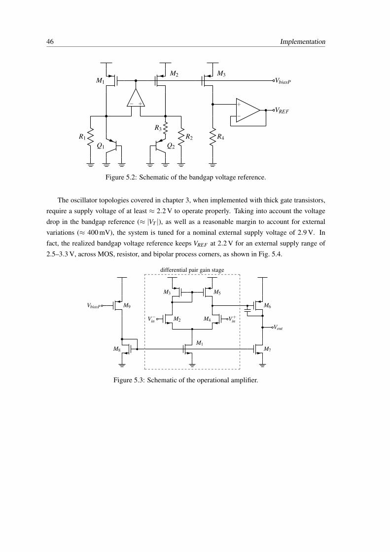
46 Implementation
− +
M1
M2
R1Q1
R2Q2
R3
M3
R4
−
+VREF
VbiasP
Figure 5.2: Schematic of the bandgap voltage reference.
The oscillator topologies covered in chapter 3, when implemented with thick gate transistors,
require a supply voltage of at least ≈ 2.2 V to operate properly. Taking into account the voltage
drop in the bandgap reference (≈ |VT |), as well as a reasonable margin to account for external
variations (≈ 400 mV), the system is tuned for a nominal external supply voltage of 2.9 V. In
fact, the realized bandgap voltage reference keeps VREF at 2.2 V for an external supply range of
2.5–3.3 V, across MOS, resistor, and bipolar process corners, as shown in Fig. 5.4.
M1
M2V−in
M3
M4 V+in
M5
M6
M7
Vout
M8
M9VbiasP
differential pair gain stage
Figure 5.3: Schematic of the operational amplifier.

5.2 Temperature and process compensation 47
V RE
F(V
)
Temperature (C)
TT
2.16
2.17
2.18
2.19
2.2
2.21
2.22
2.23
-40 -20 0 20 25 40 60 80 100 125
Figure 5.4: Simulation results of the bandgap output voltage VREF across supply and MOS, resistorand bipolar process corners.
5.2 Temperature and process compensation
M1VbiasP
R1
Q1
−+ R2
R3−+ Vthrm
M2
M3
M4
Vproc
−+
VCT RL
R4
R5R6
M5
thermal compensation process compensation gain/offset adjust
Figure 5.5: Schematic of TPC circuit.
The temperature and process compensation circuit is based on thermal compensation stage,
followed by a process sensor, and a final gain adjustment to set the nominal voltage to the required
levels. In the first stage, a CTAT voltage is generated through current biasing of Q1, with the output
level defined by R1. This voltage was set at 1.6 V to ensure correct operation of the following stage.
This voltage is buffered to generate the Vthrm voltage that feeds into the next stage. The feedback
resistors R2 and R3 can be used to attenuate the temperature dependent voltage, changing the TC
as required. The process sensor stage uses the quasi-orthogonal compensation circuit introduced
in chapter 4 , which imposes a voltage drop on Vthrm that is equal to the threshold voltage VT . In
the last stage, an amplifier isolates the process compensation stage output, and a feedback loop
allows gain and offset adjustment to the required nominal level of VCT RL.

48 Implementation
To tune the TPC block for 25 MHz, a straightforward approach is taken, since the tuning points
are nearly orthogonal. The value of R1 and the amplifier gain in the thermal compensation stage
are used to set the TC and nominal level of Vthrm, and the offset and gain of the output stage are
tuned to the required VCT RL levels.
5.3 Oscillator and output stage
M3
M4
M5
M6
M7
M8M2
M1VCT RL
Vout
VREF
current starved ring oscillator output buffer
Figure 5.6: Schematic of oscillator block and output buffer circuits.
The oscillator stage comprises a current starved ring oscillator controlled by the VCT RL voltage
generated in the TPC block. At the oscillator output a pair of inverters isolates the output signal
and restores the voltage to VDD levels.
5.4 Results
The final implementation of the circuit was simulated across MOS, resistor and bipolar process
corners as well as temperature variations. Over a range of -40–125C and across corner variations,
the worst case frequency deviation is 5.5%, with an average power draw of 164 µW, for a nominal
frequency of 24.8 MHz. The behaviour over temperature across is shown in Fig. 5.7 and the
simulated output waveform in Fig. 5.8.
In table 5.1, a brief comparison with other PVT insensitive oscillators using open-loop com-
pensation techniques is presented. When compared to other similar works, the proposed imple-
mentation targets a smaller process node, where greater process variability is expected, and real-
izes a fully self-sufficient system, including on-ship voltage supply. Furthermore, it achieves the
lowest power consumption when compared with other works implementing on-chip supplies. It
should also be noted that the experimental measurements are a more realistic metric of the typical
process variation, where as a worst case corner measurement is a inherently pessimistic figure of
merit.

5.4 Results 49
Freq
uenc
yde
viat
ion
(%)
Temperature (C)
TT
-8
-6
-4
-2
0
2
4
6
-40 -20 0 20 25 40 60 80 100 125
Figure 5.7: Simulation results of the compensated oscillator across MOS, resistor and bipolarprocess corners.
Volta
ge(V
)
Time (ns)
0
1
2
3
0 50 100 150 200
Figure 5.8: Simulation results of output waveform of the compensated oscillator.
Table 5.1: Comparison of open-loop PVT compensated oscillators.
Ref Process Frequency Power VDD On-chip Accuracy Measurement(V) regulation (%)
This work 90 nm 23.6 MHz 129 µW 2.5 Y 8.05 Worst case[8] 0.6 µm 680 kHz 400 µW 4 N 4.7 Experimental[11] 0.25 µm 7 MHz 1.5 mW 2.5 Y 2.64 Experimental[12] 0.18 µm 150 MHz 537 µW 1.8 N 2.29 Worst case[13] 0.18 µm 2 MHz 48 µW 1.8 Y 2.81 Experimental[16] 0.18 µm 20 MHz N/A N/A Y 2.98 Experimental


Chapter 6
Conclusions and Future Work
The design of a PVT insensitive oscillator, specially using open-loop compensation methods,
requires the understanding of each block in the system and how it behaves over process and tem-
perature corners. This becomes the key factor in the compensation scheme, as the compensation
of the blocks requires the realization of a magnitude that opposes the circuit variation over PVT
variations. Moreover, a further step is to tune each block not only for the conventional power-
performance-area trade off, but also from a design for variability perspective. In other words, each
design should be tuned as to lower the compensation effort.
In sum, this work provides a study on the key design considerations for the realization of PVT
insensitive oscillators, and presents the following contributions:
• A study on the performance of oscillator topologies across process and temperature corners
is presented. It comprises four oscillator architectures suitable for use with PVT compensa-
tion circuits, and includes circuit implementations in six process nodes from two foundries,
ranging from 28 nm to 110 nm.
• Study of the TPC circuit proposed by Sundaresan et al. [11] and proposal of a new design
flow, comprising an algorithm for automated circuit tuning and optimization. This proposed
methodology is able to optimize the TPC circuit for different types of oscillators.
• A novel quasi-orthogonal process compensation circuit is proposed, based on the concept of
systems comprising fully independent compensation for process, voltage, and temperature
variations.
• Implementation of a fully integrated PVT compensated oscillator using a novel open-loop
TPC circuit in a deep-submicron process node.
6.1 Future work
The next step in the realization process of the oscillator system would be the complete layout
design in the proposed process node. This would allow the extraction of the parasitic devices to
perform a post-layout simulation, thus validating the feasibility of the circuit for fabrication.
51

52 Conclusions and Future Work
With regards to the analysis of the oscillator blocks, a more comprehensive study on the be-
haviour of each oscillator topology could be performed, as was briefly stated in section 3.5. This
could provide a better insight on how to tune each specific oscillator architecture from a design for
variability perspective.

References
[1] P. Lall, M. G. Pecht, and E. B. Hakim, Influence of Temperature on Microelectronics andSystem Reliability. CRC Press, 1997.
[2] D. Gomez, M. Sroka, and J. Jimenez, “Process and temperature compensation for RF low-noise amplifiers and mixers,” Circuits and Systems I: Regular Papers, IEEE Transactions on,vol. 57, no. 6, pp. 1204–1211, 2010.
[3] B. Stretman, Solid State Electronic Devices, ser. Prentice-Hall electrical engineering series.Pearson Education, Limited, 1972.
[4] H. T. Bui and Y. Savaria, “A generic method for embedded measurement and compensationof process and temperature variations in SOCs,” in System-on-Chip for Real-Time Applica-tions, 2005. Proceedings. Fifth International Workshop on, 2005, pp. 557–562.
[5] I. Filanovsky, “Voltage reference using mutual compensation of mobility and threshold volt-age temperature effects,” in Circuits and Systems, 2000. Proceedings. ISCAS 2000 Geneva.The 2000 IEEE International Symposium on, vol. 5, 2000, pp. 197–200 vol.5.
[6] A. Zjajo, “Random process variation in deep-submicron CMOS,” in Stochastic ProcessVariation in Deep-Submicron CMOS, ser. Springer Series in Advanced Microelectronics.Springer Netherlands, 2014, vol. 48, pp. 17–54.
[7] M. Onabajo and J. Silva-Martinez, “Process variation challenges and solutions approaches,”in Analog Circuit Design for Process Variation-Resilient Systems-on-a-Chip. Springer US,2012, pp. 9–30.
[8] Y.-S. Shyu and J.-C. Wu, “A process and temperature compensated ring oscillator,” in ASICs,1999. AP-ASIC ’99. The First IEEE Asia Pacific Conference on, 1999, pp. 283–286.
[9] H. Banba, H. Shiga, A. Umezawa, T. Miyaba, T. Tanzawa, S. Atsumi, and K. Sakui, “ACMOS bandgap reference circuit with sub-1-V operation,” Solid-State Circuits, IEEE Jour-nal of, vol. 34, no. 5, pp. 670–674, May 1999.
[10] K. Sanborn, D. Ma, and V. Ivanov, “A sub-1-V low-noise bandgap voltage reference,” Solid-State Circuits, IEEE Journal of, vol. 42, no. 11, pp. 2466–2481, Nov 2007.
[11] K. Sundaresan, P. Allen, and F. Ayazi, “Process and temperature compensation in a 7-MHzCMOS clock oscillator,” Solid-State Circuits, IEEE Journal of, vol. 41, no. 2, pp. 433–442,2006.
[12] S. Panyai and A. Thanachayanont, “Design and realization of a process and temperature com-pensated CMOS ring oscillator,” in Electrical Engineering/Electronics, Computer, Telecom-munications and Information Technology (ECTI-CON), 2012 9th International Conferenceon, 2012, pp. 1–4.
53

54 REFERENCES
[13] H. Bhamra and P. Irazoqui, “A 2-MHZ, process and voltage compensated clock oscillator forbiomedical implantable SoC in 0.18- µm CMOS,” in Circuits and Systems (ISCAS), 2013IEEE International Symposium on, 2013, pp. 618–621.
[14] C. Kim, K. Roy, S. Hsu, R. Krishnamurthy, and S. Borkar, “A process variation compensatingtechnique with an on-die leakage current sensor for nanometer scale dynamic circuits,” VeryLarge Scale Integration (VLSI) Systems, IEEE Transactions on, vol. 14, no. 6, pp. 646–649,2006.
[15] J. Maneatis, “Low-jitter process-independent DLL and PLL based on self-biased tech-niques,” Solid-State Circuits, IEEE Journal of, vol. 31, no. 11, pp. 1723–1732, 1996.
[16] C.-C. Wang, G.-N. Sung, P.-C. Chen, and C.-L. Wey, “A transceiver front end for electroniccontrol units in FlexRay-based automotive communication systems,” Circuits and Systems I:Regular Papers, IEEE Transactions on, vol. 57, no. 2, pp. 460–470, 2010.
[17] X. Zhang, M. Mukadam, I. Mukhopadhyay, and A. Apsel, “Process compensation loops forhigh speed ring oscillators in sub-micron CMOS,” Emerging and Selected Topics in Circuitsand Systems, IEEE Journal on, vol. 1, no. 1, pp. 59–70, 2011.
[18] X. Zhang and A. Apsel, “A process compensated 3-GHz ring oscillator,” in Circuits andSystems, 2009. ISCAS 2009. IEEE International Symposium on, 2009, pp. 581–584.
[19] X. Zhang, R. Dokania, M. Mukadam, and A. Apsel, “A successive approximation basedprocess-invariant ring oscillator,” in Circuits and Systems (ISCAS), Proceedings of 2010IEEE International Symposium on, 2010, pp. 1057–1060.
[20] X. Zhang, I. Mukhopadhyay, R. Dokania, and A. Apsel, “A 46- µW self-calibrated gigahertzVCO for low-power radios,” Circuits and Systems II: Express Briefs, IEEE Transactions on,vol. 58, no. 12, pp. 847–851, 2011.
[21] M. McCorquodale, G. Carichner, J. O’Day, S. Pernia, S. Kubba, E. Marsman, J. Kuhn,and R. Brown, “A 25-MHz self-referenced solid-state frequency source suitable for XO-replacement,” Circuits and Systems I: Regular Papers, IEEE Transactions on, vol. 56, no. 5,pp. 943–956, 2009.
[22] X. Zhang and A. Apsel, “A low-power, process-and- temperature- compensated ring oscil-lator with addition-based current source,” Circuits and Systems I: Regular Papers, IEEETransactions on, vol. 58, no. 5, pp. 868–878, 2011.
[23] ——, “A low variation GHz ring oscillator with addition-based current source,” in ESSCIRC,2009. ESSCIRC ’09. Proceedings of, 2009, pp. 216–219.
[24] A. Pappu, X. Zhang, A. Harrison, and A. Apsel, “Process-invariant current source design:Methodology and examples,” Solid-State Circuits, IEEE Journal of, vol. 42, no. 10, pp.2293–2302, 2007.
[25] X. Zhang, A. Pappu, and A. Apsel, “Low variation current source for 90nm CMOS,” inCircuits and Systems, 2008. ISCAS 2008. IEEE International Symposium on, 2008, pp. 388–391.
[26] C.-Y. Yu, J.-Y. Yu, and C.-Y. Lee, “An eCrystal oscillator with self-calibration capability,”in Circuits and Systems, 2009. ISCAS 2009. IEEE International Symposium on, 2009, pp.237–240.

REFERENCES 55
[27] ——, “A low voltage all-digital on-chip oscillator using relative reference modeling,” VeryLarge Scale Integration (VLSI) Systems, IEEE Transactions on, vol. 20, no. 9, pp. 1615–1620, 2012.
[28] J. Maneatis and M. Horowitz, “Precise delay generation using coupled oscillators,” Solid-State Circuits, IEEE Journal of, vol. 28, no. 12, pp. 1273–1282, 1993.
[29] S. Bendhia, Advanced CMOS Cell Design. McGraw-Hill Education (India) Pvt Limited,2006.
[30] N. Sadeghi, A. Sharif-Bakhtiar, and S. Mirabbasi, “A 0.007- mm2 108- p±/ C 1-MHzrelaxation oscillator for high-temperature applications up to 180C in 0.13- µm CMOS,”Circuits and Systems I: Regular Papers, IEEE Transactions on, vol. 60, no. 7, pp. 1692–1701, 2013.
[31] T. Lee, The Design of CMOS Radio-Frequency Integrated Circuits. Cambridge UniversityPress, 2004.