Static Timing Analysis for Level-Clocked
8
IEEE TRANSACTIONS ON COMPUTER-AIDED DESIGN, TO APPEAR. 1 Static Timing Analysis for Level-Clocked Circuits in the Presence of Cross Talk Soha Hassoun, Senior Member, IEEE, , Christopher Cromer, Eduardo Calvillo-G´ amez, member, IEEE ) Abstract— Static timing analysis is instrumental in efficientl y verifying a design’s temporal behavior to ensure correct function- ality at the required frequency. This paper addresses static timing analysis in the presence of cross talk for circuits containing level- sensitive latches, typical in high-performance designs. The paper foc uses on two problems. Firs t, coupl ing in a seque ntial circ uit can occur because of the proximity of a victim’s switching input to any periodic occu rre nce of the aggressor’s input switchi ng windo w. This paper shows that only thre e cons ecuti ve peri odic occurrences of the aggressor’s input switching window must be con sid er ed. Sec ond, an arr iv al time in a se que nti al cir cui t is typically computed relative to a specific clock phase. The paper pro pos es a new phase shi ft operator to ali gn the aggre sso r’ s three relevant switching windows with the victim’s input signals. This paper solves the static analy sis probl em for level- cloc ked cir cuits itera tive ly in polynomi al time, and it shows an upper bound on the number of it er at ions equal to the number of capacitors in the circui t. The contributions of this paper hold for any disc rete ove rlap ping coupl ing mode l. The expe rime ntal results demonstrate that eliminating false coupling allows finding a smaller clock period at which a circuit will run. I. I NTRODUCTION Shrinking process geometries have imposed new challenges in both design and verification. One particular problem is the capacitive coupling among two or more signals in the circuit. Coupling exists due to the proximity of a wire to others that are either in the same layer (lateral coupling), or in different layers (inte r-l ayer coupl ing). Coupl ing creates undes ired noise and delay in the circuit. This phenomenon is commonly referred to as cross talk . Noise on a signal refers to creating voltage deviation from the nominal supply and ground rails when the signals should otherwise have been stable at a high or low value as dictated by the logic and delay of the circuit [21]. Noise greater than the allowed noise margins causes malfunctions. Delay variation due to capacitive coupling refers to either spe edi ng or slowing the point in ti me whe re a swi tch ing net rea che s it s receiving thre shold , thus caus ing rece ivi ng gates in the immediate fanouts to switch sooner or later than exp ect ed. The del ay va ria tio n is dependent on the rel ati ve arrival times of the victim net and the aggressor(s) net that capacitively couple to the victim. If the victim is switching in Manuscript received January 15, 2002; revised August 8, 2002. This work as supported by NSF POWRE and CAREER grants. Soha Hassoun is with the Computer Science Department at Tufts Univer sity , Medford, MA, 02155, U.S.A. Christopher X. Cromer is a senior processor designer at Infineon Technolo- gies Corp., San Jose, CA, 95512, U.S.A. Eduardo Calvillo-G´ amez is a Ph. D. St ude nt in the Compu ter Sci enc e Department at Tufts University, Medford, MA, 02155, U.S.A. the same direction as the aggressor(s), then we have assistive coupling, and the vic tim switches soo ner tha n ant ici pat ed. Delay improvements could potentially cause race-through or double-clocking conditions, and thus circuit failure. With op- posing coupling, the victim net switches later due to opposing transition on the aggressor(s) net(s). Delay degradation cause per for man ce fa ilu re; the circui t will not run at the des ire d frequ ency . Stat ic timi ng anal ysis techn iques , which verify a design’s temporal behavior to ensure correct functionality at the required frequency, thus must consider the effects of cross talk. Several static timing analysis techniques that consider cross tal k have bee n pro pos ed for combin ational cir cui ts. Some are based on itera ti ve tec hni que s [3], [18 ]; some are bas ed on the pro pagation of events [5]; others are based on mor e complex mathematical formulations [10]. The choice of what const itu tes cou pli ng (an y ove rla p of the inputs ’ swi tch ing windows v .s. more detailed coupling condition s) affe ct the complexity of the algorithms. Consideration of the functional cor rel ati on of the victim and the agg res sor s allow fur the r accuracy in ana lys is [25 ], [2] , [4] . The wor st case vic ti m delay can be obtained by driver modeling using reduced order modeling and worst case alignment of the aggressors relative to the victim [7], [9], [22]. This paper addresses cross talk analysis for circuits with lev el-s ensi tiv e latc hes. Lev el-c locke d circ uits are cert ainly dominant in high-performance designs because they can oper- ate at faster clock rates than edge-triggered circuits [8]. This is because, unlike edge-triggered registers, latches allow borrow- ing time across their boundaries. Researchers have efficiently solved the problem of verifying a clock schedule [23], [14], [11]. Howe ver , naiv ely assuming wors t case crosstalk while running these algorithms yields pessimistic clock periods. A clock schedule specifies the clock period, and the relative ti min g and durat ion of eac h of the phase s in the schedule . Given a circuit and a clock schedule, we solve the problem of clock sched ule verifica tion in the presence of cross talk. That is, we answer the question, does the circuit run at the specified clock period given the phase waveforms imposed by the clock schedule? The dif ficulty of clock schedule ver ific ati on proble m is twof ol d. Fi rs t, due to the pe ri odic nature of si gnal s in a sequential circuit, coupling can occur because of the proximity of a victim’s switching input to any periodic occurrence of the aggressor’s input switching window. More than one occurrence of the aggres sor wa vef orm thus mus t be compar ed aga ins t that of the victim. Second, the arrival times in a level-clocked cir cuit are typ ica lly comput ed rel ati ve to a spe cifi c clo ck
-
Upload
matheus-silva -
Category
Documents
-
view
238 -
download
0
Transcript of Static Timing Analysis for Level-Clocked
7/28/2019 Static Timing Analysis for Level-Clocked
http://slidepdf.com/reader/full/static-timing-analysis-for-level-clocked 1/8
IEEE TRANSACTIONS ON COMPUTER-AIDED DESIGN, TO APPEAR. 1
Static Timing Analysis for Level-Clocked Circuits
in the Presence of Cross Talk Soha Hassoun, Senior Member, IEEE,, Christopher Cromer, Eduardo Calvillo-Gamez, member, IEEE
) Abstract— Static timing analysis is instrumental in efficientlyverifying a design’s temporal behavior to ensure correct function-ality at the required frequency. This paper addresses static timinganalysis in the presence of cross talk for circuits containing level-sensitive latches, typical in high-performance designs. The paperfocuses on two problems. First, coupling in a sequential circuitcan occur because of the proximity of a victim’s switching inputto any periodic occurrence of the aggressor’s input switchingwindow. This paper shows that only three consecutive periodicoccurrences of the aggressor’s input switching window must beconsidered. Second, an arrival time in a sequential circuit istypically computed relative to a specific clock phase. The paper
proposes a new phase shift operator to align the aggressor’sthree relevant switching windows with the victim’s input signals.This paper solves the static analysis problem for level-clockedcircuits iteratively in polynomial time, and it shows an upperbound on the number of iterations equal to the number of capacitors in the circuit. The contributions of this paper holdfor any discrete overlapping coupling model. The experimentalresults demonstrate that eliminating false coupling allows findinga smaller clock period at which a circuit will run.
I. INTRODUCTION
Shrinking process geometries have imposed new challenges
in both design and verification. One particular problem is the
capacitive coupling among two or more signals in the circuit.Coupling exists due to the proximity of a wire to others that are
either in the same layer (lateral coupling), or in different layers
(inter-layer coupling). Coupling creates undesired noise and
delay in the circuit. This phenomenon is commonly referred
to as cross talk .
Noise on a signal refers to creating voltage deviation from
the nominal supply and ground rails when the signals should
otherwise have been stable at a high or low value as dictated
by the logic and delay of the circuit [21]. Noise greater than
the allowed noise margins causes malfunctions.
Delay variation due to capacitive coupling refers to either
speeding or slowing the point in time where a switching
net reaches its receiving threshold, thus causing receivinggates in the immediate fanouts to switch sooner or later than
expected. The delay variation is dependent on the relative
arrival times of the victim net and the aggressor(s) net that
capacitively couple to the victim. If the victim is switching in
Manuscript received January 15, 2002; revised August 8, 2002. This work as supported by NSF POWRE and CAREER grants.
Soha Hassoun is with the Computer Science Department at Tufts University,Medford, MA, 02155, U.S.A.
Christopher X. Cromer is a senior processor designer at Infineon Technolo-gies Corp., San Jose, CA, 95512, U.S.A.
Eduardo Calvillo-Gamez is a Ph.D. Student in the Computer ScienceDepartment at Tufts University, Medford, MA, 02155, U.S.A.
the same direction as the aggressor(s), then we have assistive
coupling, and the victim switches sooner than anticipated.
Delay improvements could potentially cause race-through or
double-clocking conditions, and thus circuit failure. With op-
posing coupling, the victim net switches later due to opposing
transition on the aggressor(s) net(s). Delay degradation cause
performance failure; the circuit will not run at the desired
frequency. Static timing analysis techniques, which verify a
design’s temporal behavior to ensure correct functionality at
the required frequency, thus must consider the effects of cross
talk.Several static timing analysis techniques that consider cross
talk have been proposed for combinational circuits. Some
are based on iterative techniques [3], [18]; some are based
on the propagation of events [5]; others are based on more
complex mathematical formulations [10]. The choice of what
constitutes coupling (any overlap of the inputs’ switching
windows v.s. more detailed coupling conditions) affect the
complexity of the algorithms. Consideration of the functional
correlation of the victim and the aggressors allow further
accuracy in analysis [25], [2], [4]. The worst case victim
delay can be obtained by driver modeling using reduced order
modeling and worst case alignment of the aggressors relative
to the victim [7], [9], [22].This paper addresses cross talk analysis for circuits with
level-sensitive latches. Level-clocked circuits are certainly
dominant in high-performance designs because they can oper-
ate at faster clock rates than edge-triggered circuits [8]. This is
because, unlike edge-triggered registers, latches allow borrow-
ing time across their boundaries. Researchers have efficiently
solved the problem of verifying a clock schedule [23], [14],
[11]. However, naively assuming worst case crosstalk while
running these algorithms yields pessimistic clock periods.
A clock schedule specifies the clock period, and the relative
timing and duration of each of the phases in the schedule.
Given a circuit and a clock schedule, we solve the problem
of clock schedule verification in the presence of cross talk.That is, we answer the question, does the circuit run at the
specified clock period given the phase waveforms imposed by
the clock schedule?
The difficulty of clock schedule verification problem is
twofold. First, due to the periodic nature of signals in a
sequential circuit, coupling can occur because of the proximity
of a victim’s switching input to any periodic occurrence of the
aggressor’s input switching window. More than one occurrence
of the aggressor waveform thus must be compared against
that of the victim. Second, the arrival times in a level-clocked
circuit are typically computed relative to a specific clock

7/28/2019 Static Timing Analysis for Level-Clocked
http://slidepdf.com/reader/full/static-timing-analysis-for-level-clocked 2/8
IEEE TRANSACTIONS ON COMPUTER-AIDED DESIGN, TO APPEAR. 2
phase. Translating the arrival times using a common reference
point will be needed to meaningfully compare the switching
windows.
This paper addresses both of these problems. We show that
only three consecutive switching windows of the aggressor’s
input must be compared with the victim’s input switching
window. To determine overlap in switching windows at the
inputs of the victim and aggressor, we propose a phase shift
operator that can translate values from the aggressor’s to the
victim’s time zones. The paper solves the clock schedule
verification problem in the presence of cross talk iteratively
in polynomial time. Furthermore, it shows an upper bound on
the number of iterations equal to the number of capacitors in
the circuit.
Several discrete and continuous coupling models are possi-
ble for representing the change in delay due to coupling. We
choose to use the dynamically bounded delay model [10], an
abstract delay model that allows a gate’s delay to be assigned
one of many values depending on related operating conditions.
While more accurate continuous models are possible, e.g. [6],
the chosen model is a generalization of discrete coupling
models, such as ones that assume a 0X, 1X, or 2X increase in
delay, e.g. [18]. While suffering from inaccuracies compared
to continuous models, discrete models require less computa-
tional complexity. Furthermore, they have proved helpful in
understanding the complex problem of static timing analysis
in the presence of cross talk. Their use in this paper allowed
us to achieve an understanding and develop a solution to the
coupling problem in level-clocked circuits. The framework and
solution proposed here can be easily extended to utilize other
discrete coupling models.
The paper is organized as follows. Section II reviews
recent advances in timing analysis for combinational circuits
in the presence of cross talk and for level-clocked circuits.Section III introduces the clock schedule model, the gate-level
delay model, and the circuit model. An example is presented
in Section IV. Timing equations to model correct circuit
operation and coupling conditions are respectively derived
in Section V and in Section VI. Then, in Section VII, we
present a polynomial algorithm to verify the timing of a level-
clocked circuit when given a clock schedule. We conclude with
experimental results.
I I . RELATED WORK
A. Timing Analysis in the Presence of Cross Talk
Timing analysis techniques for non-cyclic combinational
circuits are based on traversing an acyclic graph in a timelinear in the number of vertices and edges [13]. In the presence
of cross talk, however, such techniques cannot be directly
applied because one net can couple to another anywhere in the
circuit. Mutual dependencies among the signals are created,
effectively creating cycles in the underlying timing graph.
Iterative techniques have been proposed to solve this problem.
An initial solution is first assumed. New solutions are then
iteratively computed from previous ones, until the solution
converges.
Several researchers have proposed such iterative solutions.
Pileggi’s group at CMU model a gate driving an RC load
as a linear time-varying voltage source in series with a
resistance [9]. Their static timing analysis, TACO [3], begins
by maximizing the switching windows for each signal: the
earliest arrival times are set to zero, and the latest arrival times
are set to infinity. Static timing analysis is then run, computing
all arrival times in the circuit assuming worse case alignment
of the aggressors. Analyzing the output of this run, some
aggressors are found to be non-aligned with the victims. The
arrival times for the victims are updated and propagated using
a static timing analysis run. The process repeats to tighten
the windows until the windows stop shrinking. Sapatnekar
also proposes an iterative approach [18]. Whenever switching
windows of wires overlap, then the delays are updated. Zhou,
Shenoy and Nicholls establish a theoretical foundation for
iterative techniques for timing analysis with cross talk [26].
They show that different initial solutions lead to different
convergent solutions. They also show that the optimal fixpoint
(tightest) solution is obtained by starting from the best case
solution that assumes no coupling.
B. Verifying Clock SchedulesThe biggest challenge in formalizing the verification of
clock schedules for level-clocked circuits was creating a
general clock schedule model to reflect borrowing across latch
boundaries. Among first generation timing analysis tools, such
as TA [1], TV [12], Crystal [15], and LEADOUT [24], only
the latter correctly verified borrowing across latch boundaries.
Second generation timing analysis tools, developed in the
early nineties, are based on formalizing the timing constraints
and developing efficient algorithms to solve them. Sakallah,
Mudge, and Olukoton developed the SMO model [16] which
was widely adopted within the timing verification and op-
timization community. Ishii, Leiserson, and Papaefthymiou
also provide a general framework for the timing verification
of 2-phase level-clocked circuits [11]. Schedule verification
algorithms were based on one of two approaches. The Sakallah
et. al approach [17] and the Szymanski and Shenoy ap-
proach [23] advocate computing arrival times using iterative
approaches based on successive relaxation of arrival and depar-
ture times. Szymanski and Shenoy show that clock schedules
can be verified using a simple polynomial time algorithm
modeled after the Bellman-Ford shortest path algorithm [23].
Lockyear’s approach [14] and Ishii et. al’s approach [11], how-
ever, are based on determining the amount of time in which
a computation must complete. This approach also results in
efficient polynomial algorithms for verifying schedules.
III. PRELIMINARIES
A. Clock Schedule Model
Our clock schedule model is based on the SMO
formulation [16]. A n-phase clock schedule is an ordered
collection of n periodic signals,
φ1¡ ¢ ¢ ¢ ¡
φn ¦
, having a common
period π. Because phases are periodic, a local time zone
of width π is associated with each phase. Each phase φi
is characterized by two parameters ei and wi. Parameter eirepresents the absolute time when φi begins (relative to an
arbitrary global time reference). Parameter wi is the length
7/28/2019 Static Timing Analysis for Level-Clocked
http://slidepdf.com/reader/full/static-timing-analysis-for-level-clocked 3/8
IEEE TRANSACTIONS ON COMPUTER-AIDED DESIGN, TO APPEAR. 3
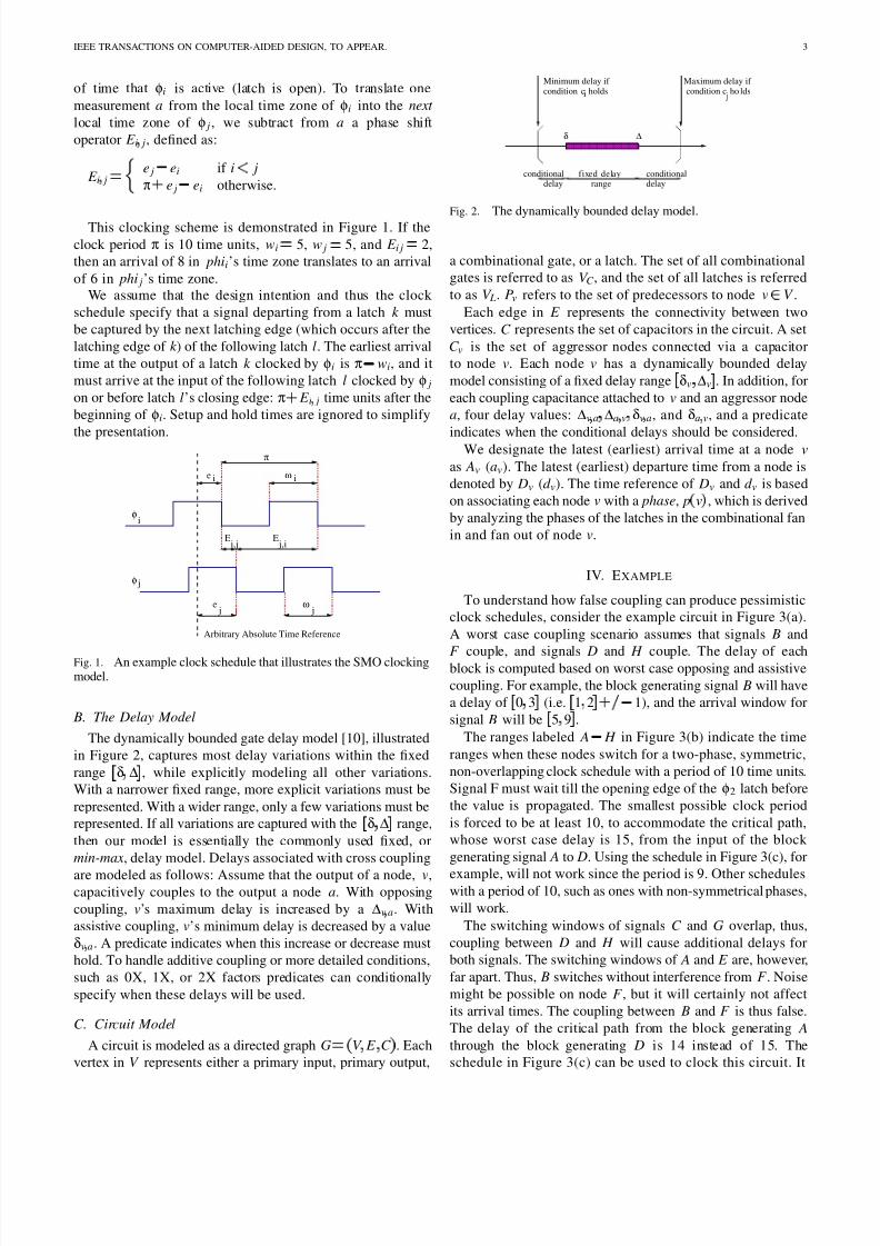
of time that φi is active (latch is open). To translate one
measurement a from the local time zone of φi into the next
local time zone of φ j , we subtract from a a phase shift
operator E i j, defined as:
E ij
¡
¢
e j£
ei if i ¤ j
π ¥ e j £
ei otherwise.
This clocking scheme is demonstrated in Figure 1. If the
clock period π is 10 time units, wi¡ 5, w j
¡ 5, and E i j¡ 2,
then an arrival of 8 in phii’s time zone translates to an arrival
of 6 in phi j’s time zone.
We assume that the design intention and thus the clock
schedule specify that a signal departing from a latch k must
be captured by the next latching edge (which occurs after the
latching edge of k ) of the following latch l. The earliest arrival
time at the output of a latch k clocked by φi is π£
wi, and it
must arrive at the input of the following latch l clocked by φ j
on or before latch l’s closing edge: π ¥ E ij time units after the
beginning of φi. Setup and hold times are ignored to simplify
the presentation.
Arbitrary Absolute Time Reference
j
j,iE
i,jE
φ
φ j
i
π
iω
ω j
e
ie
Fig. 1. An example clock schedule that illustrates the SMO clockingmodel.
B. The Delay Model
The dynamically bounded gate delay model [10], illustrated
in Figure 2, captures most delay variations within the fixed
range ¦ δ¡
Ƥ , while explicitly modeling all other variations.
With a narrower fixed range, more explicit variations must be
represented. With a wider range, only a few variations must be
represented. If all variations are captured with the¦δ
¡
Ƥ
range,
then our model is essentially the commonly used fixed, or
min-max, delay model. Delays associated with cross coupling
are modeled as follows: Assume that the output of a node, v,capacitively couples to the output a node a. With opposing
coupling, v’s maximum delay is increased by a ∆va. With
assistive coupling, v’s minimum delay is decreased by a value
δva. A predicate indicates when this increase or decrease must
hold. To handle additive coupling or more detailed conditions,
such as 0X, 1X, or 2X factors predicates can conditionally
specify when these delays will be used.
C. Circuit Model
A circuit is modeled as a directed graph G ¡
V ¡
E ¡
C ¦
. Each
vertex in V represents either a primary input, primary output,
Minimum delay if condition c holdsi
¨ ¨ ¨ ¨ ¨ ¨ ¨ ¨ ¨ ¨
¨ ¨ ¨ ¨ ¨ ¨ ¨ ¨ ¨ ¨
δ ∆
fixed delayrange
conditionaldelay delay
conditional
condition c ho lds j
Maximum delay if
Fig. 2. The dynamically bounded delay model.
a combinational gate, or a latch. The set of all combinational
gates is referred to as V C , and the set of all latches is referred
to as V L. Pv refers to the set of predecessors to node v V .
Each edge in E represents the connectivity between two
vertices. C represents the set of capacitors in the circuit. A set
C v is the set of aggressor nodes connected via a capacitor
to node v. Each node v has a dynamically bounded delay
model consisting of a fixed delay range ¦ δv ¡
∆v § . In addition, for
each coupling capacitance attached to v and an aggressor node
a, four delay values: ∆v a ¡
∆a v ¡
δv a, and δa v, and a predicate
indicates when the conditional delays should be considered.We designate the latest (earliest) arrival time at a node v
as Av (av). The latest (earliest) departure time from a node is
denoted by Dv (d v). The time reference of Dv and d v is based
on associating each node v with a phase, p
v¦
, which is derived
by analyzing the phases of the latches in the combinational fan
in and fan out of node v.
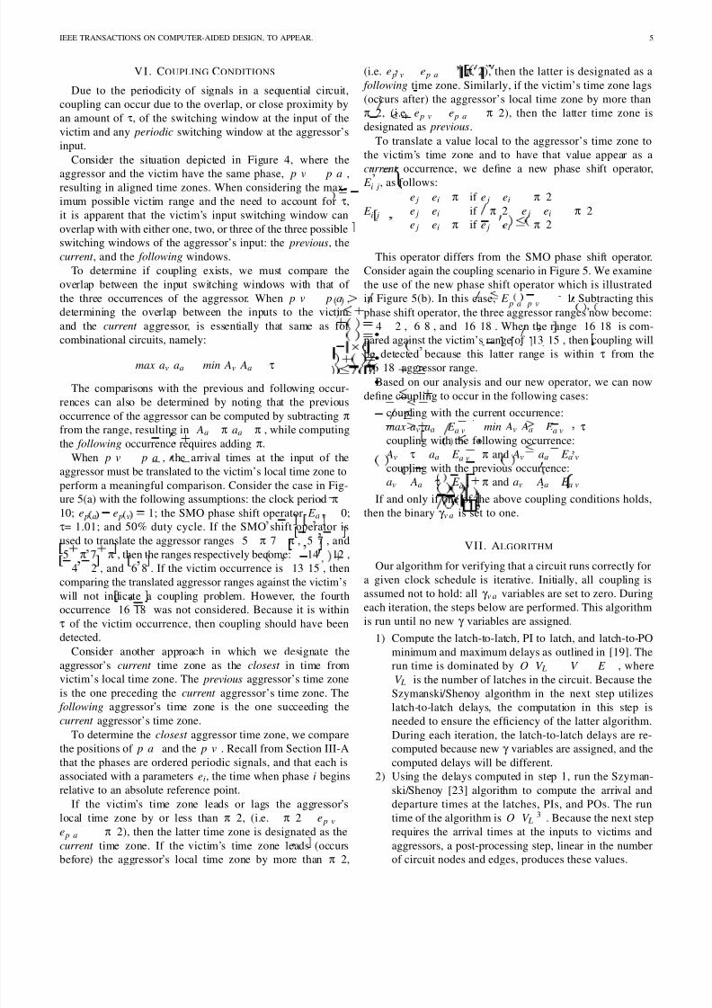
IV. EXAMPLE
To understand how false coupling can produce pessimistic
clock schedules, consider the example circuit in Figure 3(a).
A worst case coupling scenario assumes that signals B and
F couple, and signals D and H couple. The delay of eachblock is computed based on worst case opposing and assistive
coupling. For example, the block generating signal B will have
a delay of ¦0
¡
3§
(i.e.¦1
¡
2§ ¥
£
1), and the arrival window for
signal B will be¦5
¡
9§.
The ranges labeled A£
H in Figure 3(b) indicate the time
ranges when these nodes switch for a two-phase, symmetric,
non-overlapping clock schedule with a period of 10 time units.
Signal F must wait till the opening edge of the φ2 latch before
the value is propagated. The smallest possible clock period
is forced to be at least 10, to accommodate the critical path,
whose worst case delay is 15, from the input of the block
generating signal A to D. Using the schedule in Figure 3(c), for
example, will not work since the period is 9. Other scheduleswith a period of 10, such as ones with non-symmetrical phases,
will work.
The switching windows of signals C and G overlap, thus,
coupling between D and H will cause additional delays for
both signals. The switching windows of A and E are, however,
far apart. Thus, B switches without interference from F . Noise
might be possible on node F , but it will certainly not affect
its arrival times. The coupling between B and F is thus false.
The delay of the critical path from the block generating A
through the block generating D is 14 instead of 15. The
schedule in Figure 3(c) can be used to clock this circuit. It

7/28/2019 Static Timing Analysis for Level-Clocked
http://slidepdf.com/reader/full/static-timing-analysis-for-level-clocked 4/8
IEEE TRANSACTIONS ON COMPUTER-AIDED DESIGN, TO APPEAR. 4
φ1
φ1
φ2
F
G
H
φ2
φ1 φ
1
B
A
C
D
B
A
C
D
5 10 15 20
Absolute Time
5 10 15 20
Absolute Time
E
(a)
(b)
[1,2]+/−1 [1,2]+/−1[1,2] [3,4]
E GF H
Fig. 3. Example circuit and schedules. (a) Circuit under consideration.Each block has a bounded delay model: delays are expressed as arange and the conditional delay due to coupling is ¢ ¡ £ 1. (b) A clock schedule with the smallest allowed period of 10 when assuming allcoupling causes delays. (c) A clock schedule with a period of 9 whenfalse capacitive coupling between B and F is eliminated.
has a smaller period than the one in Figure 3(b). Timinganalysis that eliminates false coupling therefore allows a faster
schedule. In this example, the comparison of the overlapping
switching windows of the victims and the aggressors was done
in absolute time. However, arrival times are computed relative
to a specific latch’s time zone, and we must translate the time
zone of the aggressor to that of the victim (or vice versa) in
order to compare them correctly.
V. TIMING EQUATIONS
The earliest and latest arriving signals at the inputs of
the victim and aggressor must be analyzed to determine if
the switching windows overlap. The latest arrival time at acombinational node v:
Av¡
¢
max¥
k ¦ Pv
Dk £
E p § k p § v ¨
¦
if p
k ¦ ©
¡ p
v¦
max¥
k ¦ Pv Dk if p
k ¦
¡ p
v¦
(1)
If the phases associated with nodes k and v are different, then
the departure time Dk is adjusted by E p § k ¨ p § v ¨
to transfer the
departure time of k to v’s local time zone.
For a latch v with input k :
Av¡ max
Dk £
E p § k p § v ¨
¡
π£
w p § v ¨
¦
(2)
previous current following
p(a)
p(v)
Victim’s input switching windowaggressor’s inputswitching window
local time zonevictim’s
longest possiblevictim range
Time
aggressor’s
previous time zone current time zone
aggressor’s aggressor’s
following time zone
Fig. 4. The aggressor’s and victim’s time zones are aligned. we mustcheck for overlap between the switching windows of the inputs tothe victim and aggressor while considering all switching ranges.
Here the latest arrival time at the latch depends on the relative
arrival time of the signals at its input, Dk , and when the latch
allows the data through, π£
w p § v ¨
. If the input signal k arrives
before the latch is open, then it must wait till the latch opens
before k is passed through.The departure time from a node v, without capacitive
coupling on its output, can be specified as follows:
Dv¡ Av ¥
∆v (3)
To compute Dv, the departure time at v, we augment the latest
arriving input to v by an amount ∆v, the maximum propagation
delay through v.
For a node v with capacitive coupling on its output through
one or more aggressor in C v, the maximum departure time is:
Dv¡ Av ¥
∆v ¥ ∑¥
a
C v
γ va∆v
a (4)
This constraint ensures that the propagation delay of v is
augmented by an amount ∆va when a node v (the victim)
experiences capacitive coupling through an aggressor a. Worst
case opposing coupling between v and a is assumed because
we are not considering the functional/logical behavior of the
circuit. Variable γ v a is binary indicating if the conditions
for capacitive coupling hold. A description of conditions that
cause coupling is provided in Section VI.
We similarly specify constraints for minimum arrival and
departure times. For a combinational node v:
av
¡
¢
min¥
k ¦ Pv
d k £
E p § k p § v ¨
¦
if p
k ¦ ©
¡ p
v¦
min¥
k ¦ Pvd k if p
k ¦
¡
p
v¦
(5)
For a latch v:
av¡ max
d k £
E p § k p § v ¨
¡
π£
w p § v ¨
¦
(6)
The earliest departure time for a node v can be specified
as follows assuming worst case assistive coupling between a
victim node v and an aggressor a.
d v¡ av ¥ δv
£ ∑¥ a C v
γ v aδv a (7)
7/28/2019 Static Timing Analysis for Level-Clocked
http://slidepdf.com/reader/full/static-timing-analysis-for-level-clocked 5/8

7/28/2019 Static Timing Analysis for Level-Clocked
http://slidepdf.com/reader/full/static-timing-analysis-for-level-clocked 6/8
IEEE TRANSACTIONS ON COMPUTER-AIDED DESIGN, TO APPEAR. 6
eep(a)p(v)
p(v) p(a)π/2< e − e <− π/2
p(v)
p(a)
−20 −10 0 10
[13, 15]
−2−4−12−14 6 8
Victim’s
aggressor’s local time zone
5 7
local time zone
(a)
Victim Time
eep(a)p(v)
p(v)
p(a)
−20 −10 0 10
[13, 15]
−2−4 8
Victim’s
aggressor’s local time zone
5 7
6 16 18
local time zone
(b)
Victim Time
Fig. 5. Comparing overlapping windows: (a) Using the SMO shift operator of 9, coupling is not detected. (b) Using the new phase shiftoperator of -1, coupling is detected.
3) Compare the switching windows as outlined in the pre-vious section, and set the appropriate binary γ variables.
The run time is linear in the number of nodes, assuming
a small number of aggressors is associated with each
victim.
Our algorithm is guaranteed to converge. Once a new γ is
assigned, the victim’s window is simply stretched (the Av
becomes larger, and the av becomes smaller). Such a change
in the victim’s window can only cause other windows to
either remain the same or further stretch. The algorithm is
guaranteed to converge in
C
iterations because, in the worst
case, one γ variable is assigned true through each iteration.
Furthermore, once γ is assigned true, it does not change. Once
C
iterations are completed, no switching windows change.
The argument of continually shrinking or expanding switching
windows was used to prove convergence for timing analysis
for combinational circuits [3], [18]. Sapatnekar noted that
C
iterations are needed for convergence [18].
VIII. EXPERIMENTAL RESULTS
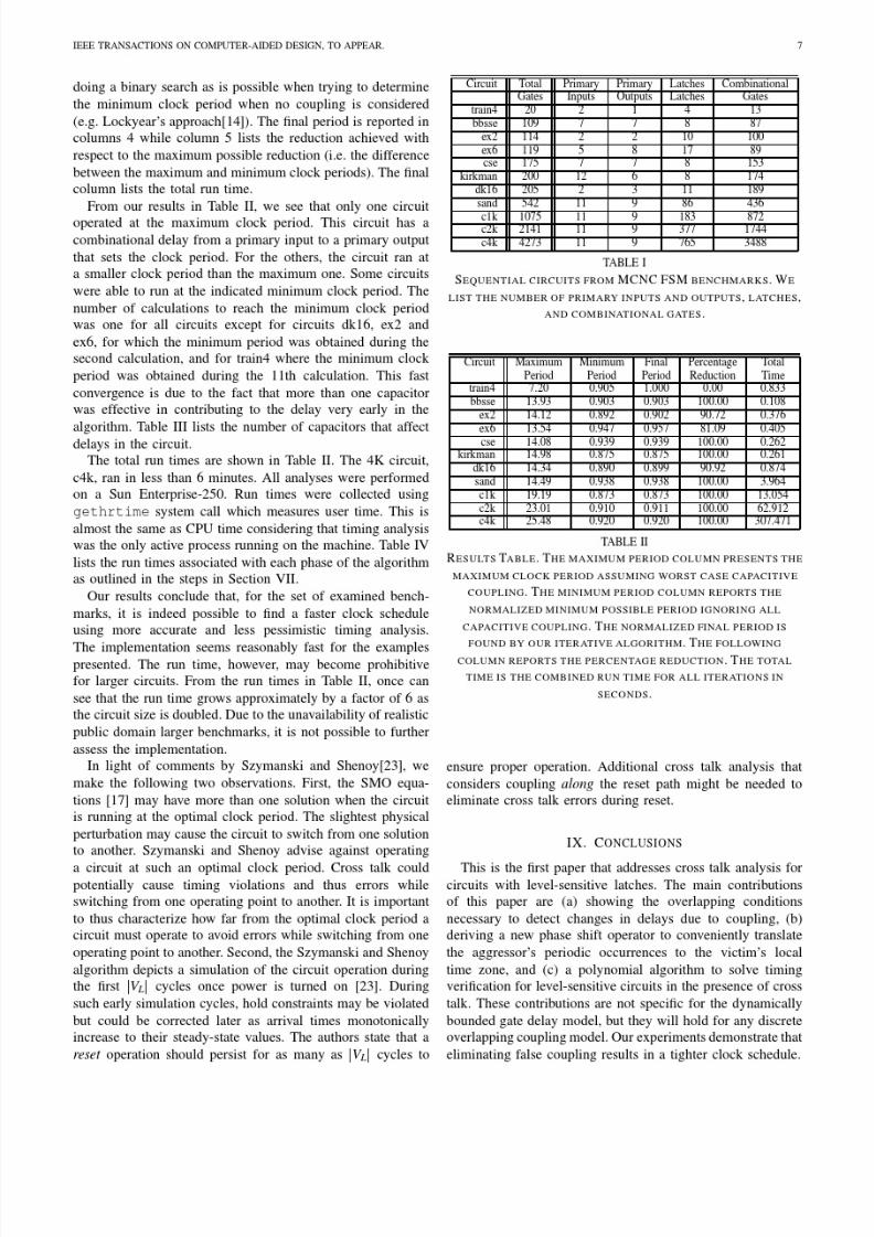
Our experiments evaluate the effectiveness of our algorithm
in verifying clock schedules in the presence of crosstalk. Our
benchmarks are based on a subset of the edge-triggered MCNC
FSM circuits that we convert to circuits with level-clocked
latches. SIS was first used to perform logic optimizationand mapping [20]. We then converted registers to back-to-
back phi1/phi2 latches and used sskew, Lockyear’s retiming
tool [14], to determine an equal, two-phase retiming and an
initial clock schedule. The combinational nodes in the circuit
were initialized with a maximum random delay within 2.5 and
0.5; the minimum delay was then initialized with a random
value that is at most 0.5 less than the maximum delay. We then
added random capacitors equal in number to 10% of the total
circuit nodes. Each capacitor was assigned a random delay
between 0.0 and 1.0. The circuits used are summarized in Ta-
ble VIII. We augmented the circuits with three larger ones: c1k,
c2k, and c4k . These circuit were obtained by stitching together
the mapped sand benchmark, and then generating delays and
capacitors randomly and converting the registers to latches.
We ran sskew to determine the worst and best clock
schedules. Table II lists the maximum period that assumes
worst case capacitive coupling, and the normalized minimum
period , which assumes no coupling, in column 2 and 3
respectively. To find the best clock period with our algorithm,
we search the space starting starting with minimum clock
period, incrementing this period by 10% of the maximum
clock period until we find a period at which the circuit ran.
Because the solution space may not be convex we avoided
7/28/2019 Static Timing Analysis for Level-Clocked
http://slidepdf.com/reader/full/static-timing-analysis-for-level-clocked 7/8

7/28/2019 Static Timing Analysis for Level-Clocked
http://slidepdf.com/reader/full/static-timing-analysis-for-level-clocked 8/8


![Statistical Static-Timing Analysis: From Basic Principles …€¦ · Statistical Static-Timing Analysis: From Basic Principles to State of the Art [1] Vladimir Todorov Moscow-Bavarian](https://static.fdocuments.us/doc/165x107/5b7c163b7f8b9a004b8e1068/statistical-static-timing-analysis-from-basic-principles-statistical-static-timing.jpg)