Spintronic Logic and Memory Devices: Prospects and...
43
Spintronic Logic and Memory Devices: Prospects and Challenges Ian Young Senior Fellow, Technology and Manufacturing Group, Director, Exploratory Integrated Circuits, Components Research Intel Corporation Hillsboro, Oregon 1 C-SPIN Workshop on Heusler Alloys for Spintronic Devices, University of Minnesota, Sept 30-31, 2015
Transcript of Spintronic Logic and Memory Devices: Prospects and...

Spintronic Logic and Memory Devices: Prospects and Challenges
Ian Young
Senior Fellow, Technology and Manufacturing Group,Director, Exploratory Integrated Circuits,
Components Research
Intel CorporationHillsboro, Oregon
1 C-SPIN Workshop on Heusler Alloys for Spintronic Devices, University of Minnesota, Sept 30-31, 2015

0
50
100
150
200
250
300
0.0 0.3 0.6 0.9
CM
OS
Cir
cuit
De
lay
(p
s)
Supply Voltage (V)
Why are we looking beyond CMOS?
Computation Efficiency needs max. performance at lowest supply (Vdd)
• Switching Energy a CVdd2
• At Vdd ≤ Vth , performance suffers significantly
• Lowest Vth is limited by leakage
• Computation efficiency of CMOS limited by 60 mV/dec Id/Vgs
sub-threshold Slope
For ITRS LG=20nmAt 1nW Standby Power
2 C-SPIN Workshop on Heusler Alloys for Spintronic Devices, University of Minnesota, Sept 30-31, 2015

Agenda
1) Introduction
the need for a Beyond-CMOS Logic Device
2) Spintronics and All-Spin Logic
Operation
Modeling
Spin Logic Circuit Simulation
3) Materials and Interfaces to enable scaling
3 C-SPIN Workshop on Heusler Alloys for Spintronic Devices, University of Minnesota, Sept 30-31, 2015

Barriers, Collectives, Thermodynamics
Generic Electronic Switch
source gate drain
e-
Energy
θ0/ 2
Generic Spintronic Switch
-V
+V
kT
Ve
offon eII
kTHVME ks 60~2
10kTVNeE 4000~
Generic Electronic Switch Generic Spintronic Switch
Barrier 20 kT at Vdd = 0.5 V 60 kT (Non-volatile)
Voltage 0.5 – 1 V 10-100 mV
Switching Energy N*20kT, N=200 electrons 60-80 kT
Phenomenon Non collective Collective
e-
4 C-SPIN Workshop on Heusler Alloys for Spintronic Devices, University of Minnesota, Sept 30-31, 2015

2. Spin Logic and Circuit Exploration
5 C-SPIN Workshop on Heusler Alloys for Spintronic Devices, University of Minnesota, Sept 30-31, 2015

Nature Physics 4, 851 - 854 (2008)
Spin logic device based on spin torque
Injected current
x
yz
Vsp
FM1 FM2
Output
ASL-Purdue, STMG-Intel
Proposed all spin logic device
C-SPIN Workshop on Heusler Alloys for Spintronic Devices, University of Minnesota, Sept 30-31, 2015
6

Metal Gnd
LGOxide
Vσp Supply Voltage Plane
LC
Tm
Tc
Side View
Lm
An example Spin logic device schematic
Copper
Copper
CopperCoFeB CoFeB
Vσp < 0, Non-Inverting Gate
The dominant magnet injects net spin into the output forcing output to align
C-SPIN Workshop on Heusler Alloys for Spintronic Devices, University of Minnesota, Sept 30-31, 2015
7

Exploring Spin Logic Devices
1. Modeling the spin devices and circuits
2. Extracting the scaling methods for spin logic (using 1)
3. Realizing the materials and interfaces (guided by 2)
C-SPIN Workshop on Heusler Alloys for Spintronic Devices, University of Minnesota, Sept 30-31, 2015
8

Describing Spin currents, Voltages, Conductances
N1 N2
1V 2V
B12
Vector spin current is the net flow of vector magnetic moment between the
nodes
Spin voltage is proportional to the net spin population
21
21
21
21
....
....
....
....
szsz
sysy
sxsx
sz
sy
sx
c
VV
VV
VV
VV
I
I
I
IA spin conductance relates vector spin
voltages to vector spin currents
Spin circuit theory is simply the book keeping of spin currents imposed by spin transport
C-SPIN Workshop on Heusler Alloys for Spintronic Devices, University of Minnesota, Sept 30-31, 2015
9

1 2
3
V3 3 0 1RF1 1 3 GF1RF2 2 3 GF2Rst1 1 4 GsetRst1 4 6 GsetRsft 4 0 GsftRst1 2 5 GsetRst1 5 6 GsetRsft 5 0 GsftRst1 6 7 GsetGRstsft1 7 0 GfttG0
Spin net list
spsp I
V
V
V
V
V
V
V
V
O
O
O
O
O
O
O
7
6
5
4
3
2
1
DC
BG
Current Sources
Voltage Sources
Node Voltages
Manipatruni, S., Nikonov, D. E., & Young, I. A. (2012). Modeling and Design of Spintronic Integrated Circuits. Circuits and Systems I: Regular Papers, IEEE Transactions on, 59(12), 2801-2814.
Inverting/Non-inverting Gate : “spin-SPICE” Example
C-SPIN Workshop on Heusler Alloys for Spintronic Devices, University of Minnesota, Sept 30-31, 2015
10

Inverting Gate : “spin-SPICE” Results
10 mV
Delay = 0.5 nsEnergy = 7.2 fJE x D = 3.6 fJ.ns, ~0 leakage7 year retention time
C-SPIN Workshop on Heusler Alloys for Spintronic Devices, University of Minnesota, Sept 30-31, 2015
11

Majority Logic input [1 1 0] Output [1]
In1 In2 In3 Major Minor
1 1 1 1 0
1 1 0 1 0
1 0 1 1 0
1 0 0 0 1
0 1 1 1 0
0 1 0 0 1
0 0 1 0 1
0 0 0 0 1
Spin Logic is compatible with high fan in logic
-V
+V
Calayir, V., Nikonov, D., Manipatruni, S., & Young, I. A. TCAS 2013
C-SPIN Workshop on Heusler Alloys for Spintronic Devices, University of Minnesota, Sept 30-31, 2015
12

Spin State Elements and Machines
Spin State
Register
OutputLogic
All Spin Combinatorial
Logic
Clock (Synchronous Circuits)Logic (Asynchronous Circuits)
Outputs (Λ)
Spin Currents
Spin Currents
Spin Currents
Spin Currents
SpinCurrents
Inputs (Σi)
States (S)
Output (G: Si-1 X Σi-> Λi) Mealy Machine
(G: Si-1 -> Λi) Moore MachineTransition (T: Si-1 X Σ-> Si)
All Spin State Machine
State element is an essential but often overlooked component.
C-SPIN Workshop on Heusler Alloys for Spintronic Devices, University of Minnesota, Sept 30-31, 2015
13

Spin State Elements
Vσp
Gnd
FM2 FM3
Output
FM1
PM
SSL
Input
Control (Magnetic)
SSE Disabled FM1 = [-1 0 0]
SSE enabled FM1 = [1 0 0]
State elements combined with combinatorial logic and interconnectsform a full synchronous compute family.
C-SPIN Workshop on Heusler Alloys for Spintronic Devices, University of Minnesota, Sept 30-31, 2015
14

Exploring Spin Logic Devices
1. Modeling the spin devices and circuits
2. Extracting the scaling methods for spin logic (using 1)
3. Realizing the materials and interfaces (guided by 2)
C-SPIN Workshop on Heusler Alloys for Spintronic Devices, University of Minnesota, Sept 30-31, 2015
15

Method 1: Scaling with PMA for Spin Logic Devices
Vsp
Gnd
FM1FM2
Vsp
Gnd
FM1FM2
PMA
Inplane
Perpendicular magnetic materials are a wide class of materials with promising performance improvement for area and Energy-Delay
Manipatruni, Sasikanth, Dmitri E. Nikonov, and Ian A. Young. "Material Targets for Scaling All Spin Logic." arXiv preprint arXiv:1212.3362 (2012).
C-SPIN Workshop on Heusler Alloys for Spintronic Devices, University of Minnesota, Sept 30-31, 2015
16
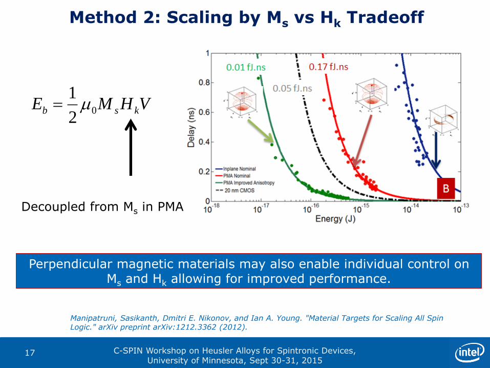
Method 2: Scaling by Ms vs Hk Tradeoff
Perpendicular magnetic materials may also enable individual control on Ms and Hk allowing for improved performance.
VHME ksb 02
1
Decoupled from Ms in PMA
Manipatruni, Sasikanth, Dmitri E. Nikonov, and Ian A. Young. "Material Targets for Scaling All Spin Logic." arXiv preprint arXiv:1212.3362 (2012).
C-SPIN Workshop on Heusler Alloys for Spintronic Devices, University of Minnesota, Sept 30-31, 2015
17

Method 3: Scaling by Interface Engineering
Interface properties play a very critical role in the net performance of the device.
Manipatruni, Sasikanth, Dmitri E. Nikonov, and Ian A. Young. "Material Targets for Scaling All Spin Logic." arXiv preprint arXiv:1212.3362 (2012).
C-SPIN Workshop on Heusler Alloys for Spintronic Devices, University of Minnesota, Sept 30-31, 2015
18

Opportunity for material exploration : ASL Material Scaling Methods
Reference: Manipatruni, Sasikanth, Dmitri E. Nikonov, and Ian A. Young. "Material Targets for Scaling All Spin Logic." arXiv preprint arXiv:1212.3362 (2012).
C-SPIN Workshop on Heusler Alloys for Spintronic Devices, University of Minnesota, Sept 30-31, 2015
19

Delay, ps100 101 102 103 104
Energ
y,f
J
10-4
10-3
10-2
10-1
100
101
CMOS HP
CMOS LV
ITFET
FEFET
Inpl ASL
STT/DW
SMG
STOlogic
SWD
NML
NAND2
CMOS LP
PMA ASL
PMA imp Anis
PMA imp Anis+Gmix
CMOS ref
Electronic
Spintronic
Ferroelectric
Orbitronic
Straintronic
ASL Imporvement
D. E. Nikonov, I. A. Young, IEEE Journal on Exploratory Solid-State Computational Devices and Circuits, 2015

Exploring Spin Logic Devices
1. Modeling the spin devices and circuits
2. Extracting the scaling methods for spin logic (using 1)
3. Realizing the materials and interfaces (guided by 2)
C-SPIN Workshop on Heusler Alloys for Spintronic Devices, University of Minnesota, Sept 30-31, 2015
21

Materials and Interfaces Play A Critical Role in Spin Devices
Ab-initio models with strong experimental co-ordination is essential to discover and engineer spintronic materials for devices.
Nature Materials 3, 868 - 871 (2004) A. Roy, D. Nikonov, I.A. Young, JAP 2011
Appl. Phys. Lett. 91, 062516 (2007)
Example 1 : Δ1 spin filtering in MgO
C-SPIN Workshop on Heusler Alloys for Spintronic Devices, University of Minnesota, Sept 30-31, 2015
22

Materials And Interfaces Play A Critical Role in Spin Devices
Ab-initio models with strong experimental co-ordination is essential to discover and engineer spintronic materials for devices.
Fe
Co
a=b=c=2.845A
FeCo
a=b=4.034A c = 2.841A
Fe3Co
Example 2 : Sensitivity in Fe-Co Phase diagram
C-SPIN Workshop on Heusler Alloys for Spintronic Devices, University of Minnesota, Sept 30-31, 2015
23

3. Improving All Spin Logic with New Materials
C-SPIN Workshop on Heusler Alloys for Spintronic Devices, University of Minnesota, Sept 30-31, 2015
24

Heusler Alloys : Magnetic Material For Scaled Spin Valves
Heusler alloys enable high intrinsic spin polarization 70 % - ~100%Without the need for tunneling electrodes. Path for highly scaled (10 nm dots) with RA < 0.1 Ohm.um2
Majority band structure
From DFT+U (solid) and EHT (dashed)
Minority band structure
From DFT+U (solid) and EHT (dashed)
EHT Modeling of Transport in Heusler spin devices, G. Shine et al SISPAD 2014
X2YZ
C-SPIN Workshop on Heusler Alloys for Spintronic Devices, University of Minnesota, Sept 30-31, 2015
25

Heusler alloys enable 1. High intrinsic spin polarization -> 70 % - ~100%2. High perpendicular magnetic anisotropy (Hk> 10000 Oe)3. High injection efficiency with no tunnel barrier
EHT Modeling of Transport in Heusler spin devices, G. Shine SISPAD 2014
High PMA due to tetragonal structure
Magnetic moment :VASP* calc. = 1.745 µB
partial magnetic moments (Bohr magnetons): Atom s p d total Mn#1 -0.037 -0.030 -2.692 -2.759 Mn#2 0.018 -0.014 2.224 2.255 x2Ga -0.020 -0.032 0.004 -0.048
Low Ms Due to compensation.
Heusler Alloys: Magnetic Material Mn3Ga For Scaled Spin Valves
* DFT tool
C-SPIN Workshop on Heusler Alloys for Spintronic Devices, University of Minnesota, Sept 30-31, 2015
26

Heusler Alloy Magnetic Devices for Spin Logic
Appl. Phys. Lett. 100, 052405 (2012)
Material GMR/TMR Hk
CoFeB -/100-200% 3000 Oe
Co2FeAl -/650% 1000 Oe
CoFe2Si - 1000 Oe
Co2FeAl0.5Si0.520 %/800% 1000 Oe
Co2Mn1.29Al -/1100 % 1000 Oe
Mn3-xGa - 10000 Oe
Co2FeGe0.5Ga0.540 % 1000 Oe
Co2Mn(Ga0.25 Ge0.75) 12.2 % 1000 Oe
Co2Fe0.4Mn0.6Si 70 % GMR 1000 Oe
Need to integrate Heuslers in MRAM and Spintronics for1. Low Ms and high Hk -> Improved retention / Write Error rate2. Improve spin Polarization -> higher GMR 3. Lower RA to enable voltage scaling VALUE PROPOSITION FOR HEUSLERS
C-SPIN Workshop on Heusler Alloys for Spintronic Devices, University of Minnesota, Sept 30-31, 2015
27
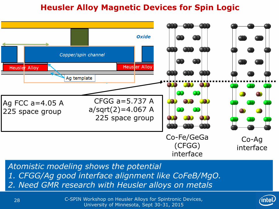
Heusler Alloy Magnetic Devices for Spin Logic
Atomistic modeling shows the potential 1. CFGG/Ag good interface alignment like CoFeB/MgO.2. Need GMR research with Heusler alloys on metals
Ag FCC a=4.05 A225 space group
CFGG a=5.737 A a/sqrt(2)=4.067 A
225 space group
Co-Ag interface
Co-Fe/GeGa(CFGG) interface
C-SPIN Workshop on Heusler Alloys for Spintronic Devices, University of Minnesota, Sept 30-31, 2015
28

An Outlook for scaling MRAM/Spin Logic
For PMA, Dot size sets Hk
volumetHME ksb 02
1 kH
Nominal Ms=106 A/m
RA scaling - Dot Scaling
2
4
d
RAR
round
p
RA
Resistance of MTJ scales with d2 at fixed RA.Write voltage (AP-P) scales as square of dot diameter at fixed RA.
VIVTMRd
RAV drive
round
MTJAp 9.0)(1)(42
Voltage scaling
Polarization loss around 0.9V
C-SPIN Workshop on Heusler Alloys for Spintronic Devices, University of Minnesota, Sept 30-31, 2015
29

A Heusler based Outlook for scaling MRAM/Spin Logic
For PMA, Dot size sets Hk
volumetHME ksb 02
1 knH
RA scaling - Dot Scaling
2
4
d
RAR
round
p
10
TMRGMR
RARA
The above described Heusler alloy scaling path may provide a way to continued scaling.
VIVGMRd
RAV drive
round
MTJAp 1.0)(1)(42
Voltage scaling
Polarization loss around 0.1V
n
M s
C-SPIN Workshop on Heusler Alloys for Spintronic Devices, University of Minnesota, Sept 30-31, 2015
30

Components for all spin logic
Conclusion
• Functional blocks for an all spin logic exist & are verified bysimulations.
• Material optimization may enable ASL energy-delay comparablewith CMOS with added non-volatility & logic efficiency.
• Material and interface understanding with ab-initio models andexperiments are the key to enabling spin logic.
2 aJ.ns
50 aJ.ns 170 aJ.ns
C-SPIN Workshop on Heusler Alloys for Spintronic Devices, University of Minnesota, Sept 30-31, 2015
31

…..and one more thing!
32 C-SPIN Workshop on Heusler Alloys for Spintronic Devices, University of Minnesota, Sept 30-31, 2015

Non-volatility for Embedded Memory and Logic:
C-SPIN Workshop on Heusler Alloys for Spintronic Devices, University of Minnesota, Sept 30-31, 2015
33

Magnetic Energy Landscape and Noise
Origin of the magnetic retention/write/read failure is thermal noise which continuously perturbs the magnet’s internal field.
Energ
y (
kT)
Angle (Degrees)
Energy Barrier
y
x
θ
ab
a>b
C-SPIN Workshop on Heusler Alloys for Spintronic Devices, University of Minnesota, Sept 30-31, 2015
34

Switching Speed of MRAM/STT Comprehending Dynamic Variations
Write Time Distribution
Write Error RateMonte-Carlo & Fokker-Planck
MC
FPA75 kT
65 kT
50 kT
75 kT
65 kT
50 kT
TED 2012 Butler et alDynamic variations set the switching
Speed for MRAM.
C-SPIN Workshop on Heusler Alloys for Spintronic Devices, University of Minnesota, Sept 30-31, 2015
35

Modeling Langevin Noise: Write Error Rates
Langevin Noise model provides a strong variability limitation to MTJ operating speed.
FP Analytical
)(1
][ 1111
1101
s
s
eff ImmeNt
mmHm
t
m
a
NoiseHTH effeff )(
Time (normalized)
Wri
te E
rror
Rate
Butler, Fischer et al TMAG Dec 2012
C-SPIN Workshop on Heusler Alloys for Spintronic Devices, University of Minnesota, Sept 30-31, 2015
36
1
)2ln( 00
cII

Write and Read Error Rates in STT/MRAM
Read Error RateWrite Error Rate
1.9X10⁻⁸ (5.5 σ for 6 MB)
9.9X10⁻¹⁰ (6σ for 120 MB)
Write Pulse Width (normalized) Read Pulse Width (normalized)
Dynamic variations can be a significant factor in the performance of spin logic/memory. Accurate modeling is required to quantify and mitigate.
e.g. Butler, Fischer et al TMAG Dec 2012
C-SPIN Workshop on Heusler Alloys for Spintronic Devices, University of Minnesota, Sept 30-31, 2015
37

Write and Read Error Rates in MRAM
Read Error RateWrite Error Rate
1.9X10⁻⁸ (5.5 σ for 6 MB)
9.9X10⁻¹⁰ (6σ for 120 MB)
Write Pulse Width (normalized) Read Pulse Width (normalized)
Write and read of an MRAM bit is not ideal. A simple reset would not be sufficient. Hence a quantitative scheme for retention error management is necessary.
e.g. Butler, Fischer et al TMAG Dec 2012
C-SPIN Workshop on Heusler Alloys for Spintronic Devices, University of Minnesota, Sept 30-31, 2015
38

Resetting MRAM can enable low retention failure rate
Ideal Scenario with Ideal resetAssuming WER=0, RER=0
Resetting the probability every 1 s
Example failure target
Finite read error rate and finite write error rate complicate the scenarios.
Manipatruni, Nikonov, Young MMM 2015
C-SPIN Workshop on Heusler Alloys for Spintronic Devices, University of Minnesota, Sept 30-31, 2015
39

(Scenario 1) Resetting MRAM: RDR>WER
Case 1 (RDR > WER): read, ECC and Rewrite of all bits is preferred.
RER of 10-12
WER of 10-13
Read Disturb
Write Error
Manipatruni, Nikonov, Young MMM 2015
C-SPIN Workshop on Heusler Alloys for Spintronic Devices, University of Minnesota, Sept 30-31, 2015
40

(Scenario 1) Resetting MRAM: RDR>WER
If (RDR > WER): read, ECC and Rewrite of all bits is preferred. This is highly energy inefficient.
RER of 10-12
WER of 10-13
Read Disturb
Write Error
Manipatruni, Nikonov, Young MMM 2015
C-SPIN Workshop on Heusler Alloys for Spintronic Devices, University of Minnesota, Sept 30-31, 2015
41

(Scenario 2) Resetting MRAM: RDR<WER
Case 2 (RDR<WER) : Read, ECC and Rewrite of the failing bit only is preferred.
If RDR < WER, an energy efficient method for MRAM reset can be implemented.
RER of 10-14
WER of 10-13
Write Error
Read Disturb
Manipatruni, Nikonov, Young MMM 2015
C-SPIN Workshop on Heusler Alloys for Spintronic Devices, University of Minnesota, Sept 30-31, 2015
42

Components for all spin logic
Conclusion
• Functional blocks for an all spin logic exist & are verified bysimulations.
• Material optimization may enable ASL energy-delay comparablewith CMOS with added non-volatility & logic efficiency.
• Material and interface understanding with ab-initio models andexperiments are the key to enabling spin logic.
2 aJ.ns
50 aJ.ns 170 aJ.ns
C-SPIN Workshop on Heusler Alloys for Spintronic Devices, University of Minnesota, Sept 30-31, 2015
43