Optimisation of Heusler Alloy Thin Films for Spintronic ...etheses.whiterose.ac.uk/4501/1/James...
148
Optimisation of Heusler Alloy Thin Films for Spintronic Devices James Sagar Submitted for the Degree of Doctor of Philosophy The University of York Department of Physics July 2013
Transcript of Optimisation of Heusler Alloy Thin Films for Spintronic ...etheses.whiterose.ac.uk/4501/1/James...
Optimisation of Heusler Alloy
Thin Films for Spintronic Devices
James Sagar
Submitted for the Degree of Doctor of Philosophy
The University of York
Department of Physics
July 2013

Abstract
Page 2
Abstract
Heusler alloys are one of the leading candidate material classes for achieving high spin
polarisation. A number of Co-based Heusler alloys are predicted to be half-metallic
ferromagnets that would theoretically provide 100% spin polarisation at the Fermi
energy. However, there are yet to be any reports of this 100% spin polarisation
experimentally. To develop these materials as a viable spin source their magnetic and
structural properties must be fully characterised and optimised.
In this study both epitaxial and polycrystalline thin films have been deposited
and their structural and magnetic properties studied in detail using a wide variety of
magnetometry and electron microscopy techniques. The polycrystalline films form an
amorphous matrix in the as-deposited state which crystallises into ordered grains
after annealing at 235°C. These films have a wide range of magnetic and structural
properties due to the crystallisation processes. Films are found to exhibit
magnetisation reversal by both single domain particle rotation and domain wall
processes which lead to coercivities ranging from 100 Oe to 2000 Oe. The individual
grains themselves are found to be highly ordered into the B2 or L21 crystal phases. In
the single crystal films long range L21 ordering is observed, the extent of which
increases monotonically with annealing temperature. These films also show extremely
low coercivities <30 Oe. The magnetisation reversal is controlled by a series of misfit
dislocations at the film substrate interface which could make these films potentially
unsuitable for device applications.
To control the magnetic and structural properties a number of seed layers
have been tested. Ag seed layers were found to reduce the coercivity of the
polycrystalline films to similar values to those found for the singe crystal films (Hc <50
Oe). The Ag seed layer exhibits island growth resulting in Co2FeSi grain segregation
which reduces the loop squareness. The island growth can be removed and the
squareness restored through the use of Cr buffer layers before the Ag layers. This
reduces film roughness to sub 1 nm therefore approaching the conditions that are
required for device fabrication.

Contents
Page 3
Contents
Abstract ............................................................................................................................................................ 2
Contents ............................................................................................................................................................ 3
List of Figures ................................................................................................................................................. 7
Acknowledgments ....................................................................................................................................... 10
Declaration .................................................................................................................................................... 11
Chapter 1. Introduction .................................................................................................................... 12
1.1. Spintronics ................................................................................................................................. 12
1.2. Magnetoresistance ................................................................................................................. 14
1.3. Spin Transfer Torques .......................................................................................................... 16
1.4. Half Metallic Ferromagnets ................................................................................................ 18
1.5. Heusler Alloys in Magnetoresistive Devices ................................................................ 19
1.6. Notes on Units and Errors ................................................................................................... 20
Chapter 2. Magnetism of Heusler Alloy Thin Films ............................................................... 21
2.1. Exchange Interactions .......................................................................................................... 21
2.1.1. Direct Exchange ............................................................................................................. 21
2.1.2. Indirect Exchange.......................................................................................................... 23
2.2. Magnetic Anisotropies .......................................................................................................... 25
2.2.1. Magnetocrystalline Anisotropy ............................................................................... 25
2.2.2. Shape Anisotropy .......................................................................................................... 26
2.3. Magnetic Domains and Single Domain Particles ........................................................ 28
2.3.1. Domain Formation ........................................................................................................ 28
2.3.2. Domain Walls .................................................................................................................. 29
2.3.3. Formation of Single Domain Particles .................................................................. 31
2.4. Magnetisation Reversal Processes................................................................................... 31
2.4.1. Domain Wall Motion .................................................................................................... 31
2.4.2. Hindrances to Domain Wall Motion ...................................................................... 33
Contents
Page 4
2.4.3. Magnetisation Rotation .............................................................................................. 34
2.5. Magnetic Activation Volumes ............................................................................................ 36
2.5.1. Magnetic Viscosity ........................................................................................................ 36
2.5.2. The Fluctuation Field and the Activation Volume ........................................... 37
2.5.3. The Activation Volume in Heusler Alloy Thin Films ....................................... 38
Chapter 3. Co-Based Heusler Alloys ............................................................................................ 39
3.1. The Heusler Structure and the Origins of Magnetism ............................................. 39
3.1.1. Crystal Structure and Disordered Phases ........................................................... 39
3.1.2. The Origin of Half Metallicity ................................................................................... 40
3.1.3. Generalised Slater Pauling Behaviour in Heusler Alloys .............................. 43
3.2. The Effects of Structural Disorder in Heusler Alloys ............................................... 45
3.2.1. Magnetic Properties ..................................................................................................... 45
3.2.2. Half-Metallicity ............................................................................................................... 46
3.3. The Effects of Surfaces and Interfaces on Half Metallicity ..................................... 49
3.4. Experimental Observations of Heusler Alloy Spin Polarisation .......................... 51
Chapter 4. Growth and Structural Characterisation ............................................................. 53
4.1. Techniques for Heusler Alloy Growth ............................................................................ 53
4.1.1. High Target Utilisation Sputtering ......................................................................... 53
4.1.2. Heusler Alloy Growth .................................................................................................. 55
4.1.3. Magnetron Sputtering ................................................................................................. 56
4.2. Structural Characterisation ................................................................................................ 57
4.2.1. Transmission Electron Microscopy (TEM) ......................................................... 57
4.2.2. Selected Area Electron Diffraction (SAED) ......................................................... 61
4.2.3. High Resolution TEM with Aberration Correction .......................................... 63
4.2.4. Scanning TEM (STEM) and its Application for Heusler Alloys. .................. 65
4.2.5. X-Ray Diffraction and its Applications for Heusler Alloys ............................ 68
Chapter 5. Magnetic Characterisation ......................................................................................... 70

Contents
Page 5
5.1. The Alternating Gradient Force Magnetometer (AGFM) ........................................ 70
5.1.1. Background ...................................................................................................................... 70
5.1.2. The Effect of Gradient Coils ....................................................................................... 73
5.1.3. AGFM Measurement Techniques ............................................................................ 75
5.2. Vibrating Sample Magnetometer (VSM) ....................................................................... 80
Chapter 6. The Effect of Structure on Magnetisation Reversal ......................................... 82
6.1. Film Growth and Sample Preparation ............................................................................ 82
6.2. Structural Characterisation ................................................................................................ 83
6.2.1. Polycrystalline Films .................................................................................................... 83
6.2.2. Epitaxially Sputtered Films ....................................................................................... 93
6.3. Magnetic Properties ............................................................................................................... 97
6.3.1. Hysteresis ......................................................................................................................... 97
6.3.2. DCD Curves ................................................................................................................... 103
6.3.3. Activation Volumes .................................................................................................... 105
6.4. Comparison of Structural and Magnetic Phenomena ........................................... 108
Chapter 7. The Effect of Seed Layers on Polycrystalline Films ...................................... 111
7.1. Film Preparation .................................................................................................................. 111
7.2. Magnetic Characterisation ............................................................................................... 112
7.3. The Effect of Seed Layers on Film Structure ............................................................. 115
7.3.1. Grain Size and Structural Ordering ..................................................................... 115
7.3.2. Island Growth of Ag Seed Layers ......................................................................... 117
7.4. Control of Island growth with Cr Buffer Layers ...................................................... 119
7.5. Antiferromagnetic Seed Layers ...................................................................................... 124
7.5.1. Exchange Bias .............................................................................................................. 124
7.5.2. Film Structure .............................................................................................................. 125
7.5.3. Magnetic Measurements ......................................................................................... 126
7.5.4. Interfacial Mn Doping ............................................................................................... 128

Contents
Page 6
Chapter 8. Conclusions and Further Work ............................................................................ 131
8.1. Conclusions ............................................................................................................................ 131
8.2. Future Work ........................................................................................................................... 133
8.2.1. Observation of Domain Structures ..................................................................... 133
8.2.2. Device Fabrication ..................................................................................................... 134
List of Symbols ........................................................................................................................................... 136
List of Abbreviations ............................................................................................................................... 137
References ................................................................................................................................................... 139
List of Publications .................................................................................................................................. 146
List of Presentations ................................................................................................................................ 147

List of Figures
Page 7
List of Figures
Figure 1.1. Schematic diagram of Datta-Das Spin-FET. [8].......................................................................... 13
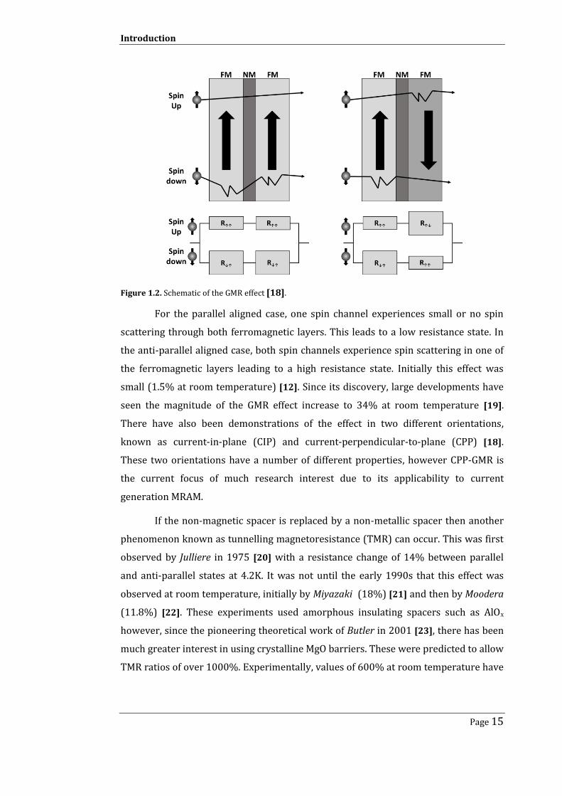
Figure 1.2. Schematic of the GMR effect [18]. .................................................................................................... 15
Figure 1.3. Schematic of the TMR effect. .............................................................................................................. 16
Figure 1.4. Schematic diagram of the spin transfer torque effect on magnetisation in a
FM/NM/FM junction. ................................................................................................................................................... 17
Figure 1.5. Schematic of the band structures for a ferromagnet and a half-metallic ferromagnet.
................................................................................................................................................................................................ 18
Figure 2.1. Dependence of the exchange integral Jex on the atomic separation ra. ............................ 22
Figure 2.2. The dependence of indirect exchange coupling on the thickness of a Cr interlayer
separating two ferromagnetic layers. ................................................................................................................... 24
Figure 2.3. Magnetised prolate spheroid. ............................................................................................................ 27
Figure 2.4. Variation of the shape anisotropy constant as a function of axial ratio for a prolate
spheroid of Co2FeSi. ...................................................................................................................................................... 27
Figure 2.5. Domain structure in a uniaxial single crystal. ............................................................................ 28
Figure 2.6. Domain structures in cubic materials ............................................................................................ 29
Figure 2.7. Schematic diagrams of 180° Bloch and Néel domain walls. ................................................ 30
Figure 2.8. Domain wall energy landscape and its effect on magnetic hysteresis. ........................... 32
Figure 2.9. Schematic of the Stoner-Wohlfarth problem for an elongated single domain particle.
................................................................................................................................................................................................ 34
Figure 2.10. Hysteresis loops for prolate spheroids with a field applied at an angle α to the easy
axis ........................................................................................................................................................................................ 35
Figure 3.1. Types of order and disorder occurring in Heusler structures ............................................ 40
Figure 3.2. Possible hybridisations between d orbitals for the minority states in the compound
Co2MnGe. ............................................................................................................................................................................ 41
Figure 3.3. Total density of states for Co2FeSi ................................................................................................... 42
Figure 3.4. The Slater-Pauling relationship ........................................................................................................ 44
Figure 3.5. Variation in the spin dependent density of states for Co2FeSi with different
quantities of disorder.. ................................................................................................................................................. 47
Figure 3.6. The effect of the lattice parameter on the minority band gap for Co2FeSi. ................... 48
Figure 3.7. Local density of states for each atom at the GaAs(110)/Co2FeSi(110) interface and
schematic of the interface .......................................................................................................................................... 49
Figure 4.1. Schematic diagram of the HiTUS system. ..................................................................................... 53
Figure 4.2. Schematic diagram of a conventional magnetron sputtering system. ............................ 56
Figure 4.3. Ray diagrams for typical TEM configurations. ........................................................................... 58
Figure 4.4. Signals generated through electron interactions with a thin specimen in a TEM. .... 59

List of Figures
Page 8
Figure 4.5. TEM images showing the interface between an epitaxially sputtered Co2FeSi film
and MgO substrate ......................................................................................................................................................... 60
Figure 4.6. SAED diffraction patterns for Heusler alloy films. ................................................................... 62
Figure 4.7. Schematic diagrams of spherical aberration from a converging lens and the effect of
using a second diverging lens to correct the aberration. ............................................................................. 64
Figure 4.8. Schematic of a STEM probe and specimen with resulting interactions ........................ 66
Figure 4.9. Bright field and HAADF STEM images of an Fe3Si/Ge interface and filtered high
resolution HAADF STEM image of a Co2FeSi film cross section ................................................................ 67
Figure 4.10. Schematic of geometries and associated angles for XRD measurements. .................. 68
Figure 5.1. Schematic diagram of a typical AGFM. .......................................................................................... 71
Figure 5.2. Noise base measurement of a typical AGFM probe. ................................................................ 73
Figure 5.3. The effect of the AC field gradient on coercivity and hysteresis loops for Co2FeSi
polycrystalline thin films taken at different alternating field gradients ............................................... 74
Figure 5.4: Coercivity of a magnetic system described through a distribution of energy barriers.
................................................................................................................................................................................................ 76
Figure 5.5. Schemetaic diagram of DC demagnetised (DCD) remanence and isothermal
remanence (IRM) curves in the context of the hysteresis loop. ................................................................ 77
Figure 5.6. Example time dependence curves. .................................................................................................. 78
Figure 5.7. The effect of pole piece separation on the AC-gradient field in the PMC micromag
2100 AGFM. ...................................................................................................................................................................... 79
Figure 5.8. Schematic diagram of ADE model 10 VSM .................................................................................. 80
Figure 6.1. Digital diffractograms from HRTEM images as well as EDX spectra for as-deposited
Co2FeSi thin films ........................................................................................................................................................... 84
Figure 6.2. Bright field TEM images and SAED patterns showing Co2FeSi grain growth at 235°C
for up to 3 hours ............................................................................................................................................................. 85
Figure 6.3. Crystallite growth process in HiTUS sputtered Co2FeSi thin films ................................... 86
Figure 6.4. Montage of bright field TEM images showing change in film structure with VB and
annealing time. ................................................................................................................................................................ 88
Figure 6.5. Grain size distributions and example TEM images for HiTUS deposited Co2FeSi
films. ..................................................................................................................................................................................... 89
Figure 6.6 TEM image of single Co2FeSi grain and schematic diagram of the [112] and [101]
faces of Co2FeSi ............................................................................................................................................................... 92
Figure 6.7. XRD scans for epitaxially sputtered Co2FeSi films. .................................................................. 93
Figure 6.8. HRSTEM image of Co2FeSi epitaxial film showing atomic ordering. ............................... 95
Figure 6.9. TEM and STEM images of a Co2FeSi/MgO interface ................................................................ 96
Figure 6.10. Hysteresis loops for polycrystalline Co2FeSi films ................................................................ 98
Figure 6.11. Schematic of the epitaxial relationship between MgO and Co2FeSi .......................... 101

List of Figures
Page 9
Figure 6.12. Hysteresis loops for epitaxially sputtered Co2FeSi thin films. ...................................... 102
Figure 6.13. Hysteresis loops and DCD remanence curves for polycrystalline and epitaxially
sputtered Co2FeSi films ............................................................................................................................................ 104
Figure 6.14. S(H) and χirr(H) curves for polycrystalline Co2FeSi sample ........................................... 106
Figure 6.15. S(H) and χirr(H) for single crystal Co2FeSi sample .............................................................. 107
Figure 6.16. Dm and Dact displayed as a function of annealing time for polycrystalline Co2FeSi
films ................................................................................................................................................................................... 108
Figure 6.17. DXRD, Dact and Ddefect displayed as a function of annealing temperature for epitaxial
Co2FeSi films. ................................................................................................................................................................. 109
Figure 7.1. Typical M-H hysteresis loops for specimens deposited with VB=250 V and VB=700 V
............................................................................................................................................................................................. 112
Figure 7.2 Variation in Hc with VB and Ms with VB for Co2FeSi films with Ag seed layers ........... 113
Figure 7.3. Graphs showing the variation of Ms and Hc with annealing time ................................... 114
Figure 7.4. Bright field TEM images and SAED pattern ............................................................................. 115
Figure 7.5. Comparison of polycrystalline Co2FeSi thin films with and without an Ag seed layer
............................................................................................................................................................................................. 116
Figure 7.6. Cross-sectional STEM image, showing island growth of Ag seed layer and Co2FeSi
film ..................................................................................................................................................................................... 117
Figure 7.7. Schematic diagram of possible epitaxial growth modes .................................................... 117
Figure 7.8. Bright field TEM image a film cross section for Cr (3 nm)/Ag (6 nm) dual seed layer
film ..................................................................................................................................................................................... 120
Figure 7.9. Hysteresis loops of polycrystalline samples with Cr/Ag seed layer and just Ag seed
layer .................................................................................................................................................................................. 121
Figure 7.10. Schematic diagram showing the difference between pinned and unpinned domain
wall motion. ................................................................................................................................................................... 122
Figure 7.11. The change in Hc with annealing time and Mr/Ms with Ag layer thickness for Cr/Ag
seed layer polycrystalline Co2FeSi films ........................................................................................................... 123
Figure 7.12. Schematic showing the directional pining of ferromagnetic spins at the F/AF
interface.. ........................................................................................................................................................................ 124
Figure 7.13. HRTEM images exchange biased Co2FeSi thin films with FFTs of Co2FeSi and IrMn
grains. ............................................................................................................................................................................... 125
Figure 7.14. Hysteresis loops of films with IrMn deposited at VB = 500 V and VB = 990 V ........ 127
Figure 7.15. Schematic of the effect of VB in the York Model of exchange bias ............................... 128
Figure 7.16. The effect of Mn interface doping on Hex ................................................................................ 129
Figure 7.17. HRSTEM images of IrMn/Co2FeSi interface .......................................................................... 130
Figure 8.1. TEM image of a potential device film .......................................................................................... 135

Acknowledgments
Page 10
Acknowledgments
This thesis and the work within would never have been possible without the help and
support of a large number of people. First and foremost I would like to acknowledge
my supervisors Dr. Atsufumi Hirohata and Prof. Kevin O’Grady. Their guidance and
support has made this all possible.
I would also like to thank the JST and EPSRC for funding the last three years.
This collaborative research grant has given me the opportunity to visit the magnetic
materials unit at the National Institute for Materials Science (NIMS) in Tsukuba. My
visits there proved fruitful and were made all the more memorable by my supervisor
there Dr. Seiji Mitani, as well as Dr. Hiroaki Sukegawa who helped to carry out all the
work there.
I have also had a lot of support from other researchers at York, particularly Dr.
Vlado Lazarov and Dr. Leonardo Lari without whom much of my microscopy would
not have been possible.
I must also thank all the residents of S/020 past and present who have made
the last three years so enjoyable. There are too many people to name them all
individually however I must make special mention to Luke who taught me how to use
most of the kit in the lab and to Ben who is always willing to join me in the pub after a
hard day.
Most of all I want to thank Laura who is there for me whenever I need her
despite being at the opposite end of the east coast mainline. She is always the voice of
reason that makes sure I keep going in the right direction. Her continued support has
given me the drive to make this possible.
Thank you all so much!
Declaration
Page 11
Declaration
I declare that the work presented in this thesis is based purely on my own research,
unless otherwise stated, and has not been submitted for a degree in this or any other
university
Signed
James Sagar
July 2013

Introduction
Page 12
Chapter 1. Introduction
Since the discovery of giant magnetoresistance (GMR) spintronics has become a field
of intense commercial and research interest. A magnetoresistive sensor can be found
in the read head of every hard disk drive sold every year. The field of spintronics
continues to grow with renewed interest and vigour as second generation magnetic
random access memory (MRAM) becomes commercially viable. All spintronic devices
need a source of spins. This is usually in the form of a ferromagnet. However, these
typical transition metal ferromagnets have low spin polarisation or low spin injection
efficiency, typically less than 50%. Half-metallic ferromagnets are a leading candidate
to replace current materials and offer much greater spin polarisation, possibly up to
100%. However there are a number of key issues that must be overcome before these
films can be used in commercial devices.
1.1. Spintronics
Today the integrated circuit and semiconductors are the backbone of modern
technology. Complementary metal-oxide-semiconductor (CMOS) and metal-oxide-
semiconductor field effect transistor (MOSFET) technologies form the building blocks
of this backbone [1]. In recent years there have been a number of astonishing
advances in this technology, driven by advances in the scalability of these devices. The
drive towards the current state of technology is due to Moore’s law [2] which states
that the number of transistors on a single chip doubles every 18 months. This has held
true for over 30 years to the point where today’s most advanced home computer
components have 7.1bn transistors per chip [3]. However, this trend cannot continue.
We are approaching the physical limit where these devices can function, either due to
high leakage currents [4] or simply the limitations of lithography to pattern them. This
technological advancement is mirrored in the magnetic storage industry where the

Introduction
Page 13
same trend is seen for areal density, information stored per unit area. However this is
beginning to plateau due to material limitations in both the hard disk and the read
head sensor. New technologies are required to overcome these difficulties and
continue the technological advance.
Spin-electronics is a promising candidate to allow further development of
current semiconductor technologies as it is widely used in the hard disk industry for
read head sensors. This means that the processes for commercialising spintronics are
already in-place. To improve spintronic devices beyond their current limitations new
materials and device technologies must be implemented. Spintronics is a field
comprising many sub disciplines although these can be broadly divided up into
semiconductor spintronics [5] and magnetoelectronics [6,7]. The latter is concerned
with all metallic systems such as magnetoresistive devices and will form most of the
foundation of this work.
Figure 1.1. Schematic diagram of Datta-Das SpinFET. [8]
Spintronics is based around the concept of using quantised angular
momentum, spin, of an electron instead of or as well as its charge. Although the effects
of the spin of the electron had been observed experimentally in the late 19th century it
was not defined until the early 20th century by Dirac. In 1857 Lord Kelvin (formally W.
Thomson) observed anisotropic magnetoresistance (AMR) [9] . AMR is the directional
dependence of the resistivity of a material relative to a magnetic field. AMR is one of
many forms of magnetoresistance which shall be discussed more thoroughly in the
next section. Since these early observations of spin dependent electron transport

Introduction
Page 14
many different devices have been designed and fabricated all using slightly different
spin dependent phenomena. The most basic and best example of the requirements of a
spintronic device is the spin field effect transistor (SpinFET) as designed by Datta and
Das [8], shown in Figure 1.1.
This work is primarily concerned with the spin source where a high spin
polarisation is required. The simplest spin source is a typical ferromagnet interfaced
with non-magnetic metal or semiconductor. The Heusler alloys used in this work are
intended for use in such a spin source. However spin generation has also been
achieved through the manipulation of magnetisation dynamics, resulting in a
phenomenon known as spin pumping [10].
1.2. Magnetoresistance
Although AMR was discovered in 1857 it was mainly of academic importance due to it
only having a small effect (a few per cent). It was used for a number of early hard disk
designs until superseded by the discovery of other magnetoresistive effects such as
giant magnetoresistance (GMR).
GMR was discovered in 1988 through electrical magnetotransport
measurements of ferromagnetic/non-magnetic/ferromagnetic multi-layered systems.
This was an attempt to further understand the dependence of interlayer exchange
coupling on the spacer thickness in thin film multilayers [11]. Grünberg [12] and Fert
[13] discovered the effect simultaneously while measuring Fe/Cr/Fe superlattices
spaced sufficiently to induce antiferromagnetic coupling between the two Fe layers.
The pair received the Nobel prize in Physics for their discovery in 2007. In their initial
publications both observed a large change in resistance for the structures when the
spaced magnetic layers were changed from anti-parallel to parallel alignment.
This was explained using the two current model initially proposed by Mott in
1936 [14,15]. Simply that the current through a transition metal can be separated into
two spin channels. This model has since been extended by Campbell [16]and Fert [17]
to include a large number of different electron scattering terms that provide better
agreement with the experimental data. This effect in a GMR multilayer is often best
explained pictorially as shown in Figure 1.2.
Introduction
Page 15
Figure 1.2. Schematic of the GMR effect [18].
For the parallel aligned case, one spin channel experiences small or no spin
scattering through both ferromagnetic layers. This leads to a low resistance state. In
the anti-parallel aligned case, both spin channels experience spin scattering in one of
the ferromagnetic layers leading to a high resistance state. Initially this effect was
small (1.5% at room temperature) [12]. Since its discovery, large developments have
seen the magnitude of the GMR effect increase to 34% at room temperature [19].
There have also been demonstrations of the effect in two different orientations,
known as current-in-plane (CIP) and current-perpendicular-to-plane (CPP) [18].
These two orientations have a number of different properties, however CPP-GMR is
the current focus of much research interest due to its applicability to current
generation MRAM.
If the non-magnetic spacer is replaced by a non-metallic spacer then another
phenomenon known as tunnelling magnetoresistance (TMR) can occur. This was first
observed by Julliere in 1975 [20] with a resistance change of 14% between parallel
and anti-parallel states at 4.2K. It was not until the early 1990s that this effect was
observed at room temperature, initially by Miyazaki (18%) [21] and then by Moodera
(11.8%) [22]. These experiments used amorphous insulating spacers such as AlOx
however, since the pioneering theoretical work of Butler in 2001 [23], there has been
much greater interest in using crystalline MgO barriers. These were predicted to allow
TMR ratios of over 1000%. Experimentally, values of 600% at room temperature have
Introduction
Page 16
been achieved by Ikeda et al. using CoFeB/MgO/CoFeB multilayer films [24]. Although
similar in many ways to GMR, TMR is fundamentally quite different.
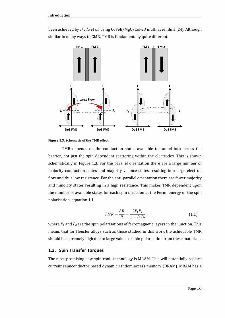
Figure 1.3. Schematic of the TMR effect.
TMR depends on the conduction states available to tunnel into across the
barrier, not just the spin dependent scattering within the electrodes. This is shown
schematically in Figure 1.3. For the parallel orientation there are a large number of
majority conduction states and majority valance states resulting in a large electron
flow and thus low resistance. For the anti-parallel orientation there are fewer majority
and minority states resulting in a high resistance. This makes TMR dependent upon
the number of available states for each spin direction at the Fermi energy or the spin
polarisation, equation 1.1.
(1.1)
where P1 and P2 are the spin polarisations of ferromagnetic layers in the junction. This
means that for Heusler alloys such as those studied in this work the achievable TMR
should be extremely high due to large values of spin polarisation from these materials.
1.3. Spin Transfer Torques
The most promising new spintronic technology is MRAM. This will potentially replace
current semiconductor based dynamic random access memory (DRAM). MRAM has a
Introduction
Page 17
large number of advantages, most importantly it is non-volatile. This means that when
the power is turned off the information is retained. 1st generation MRAM used the
Oersted field generated by a current carrying wire to write information to an array of
magnetic spin valves. The 2nd generation of MRAM will use a phenomenon known as
spin-transfer-torque (STT) as a much more efficient way to write data.
STT was first considered as a way to reverse the magnetisation in a magnetic
multilayer by Slonczewski [25]. However the effect of spin transfer had been
introduced by Berger 12 years earlier [26]. STT is easiest to consider in the case of a
ferromagnetic/non-magnetic/ferromagnetic junction like those used for GMR. The
two ferromagnetic layers have their magnetisations aligned at an angle to one
another. When electrons flow into the junction they are initially aligned or polarised
to the direction of the magnetisation in the first ferromagnetic layer. When the
electrons then travel to the second ferromagnetic layer their spins align with the
magnetisation of that layer. However as the spins align to the new direction of
magnetisation they exert a torque on that magnetisation. This is the spin transfer
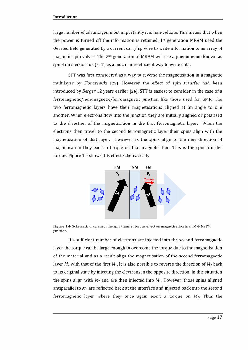
torque. Figure 1.4 shows this effect schematically.
Figure 1.4. Schematic diagram of the spin transfer torque effect on magnetisation in a FM/NM/FM junction.
If a sufficient number of electrons are injected into the second ferromagnetic
layer the torque can be large enough to overcome the torque due to the magnetisation
of the material and as a result align the magnetisation of the second ferromagnetic
layer M2 with that of the first M1. It is also possible to reverse the direction of M2 back
to its original state by injecting the electrons in the opposite direction. In this situation
the spins align with M2 and are then injected into M1. However, those spins aligned
antiparallel to M1 are reflected back at the interface and injected back into the second
ferromagnetic layer where they once again exert a torque on M2. Thus the

Introduction
Page 18
magnetisation in one ferromagnetic layer can be switched by changing the polarity of
the applied voltage. The form of the spin transfer torque is given by equation 1.2 [10]:
( )
(1.2)
Here the cross products of the magnetisations M1 and M2 give the direction of the
torque. The magnitude of the torque is then dictated by the spin polarisation of the
ferromagnets P, the saturation magnetisation Ms, the volume of the magnetic layer on
which the torque is acting V and the current applied to the junction I. γgm is the
gyromagnetic ratio. The dependence of STT on the spin polarisation of the electrodes
makes Heusler alloys a promising candidate for use in these devices due to their high
spin polarisation. A detailed examination of spin transfer torques in a large number of
systems can be found in Maekawa [27].
1.4. Half Metallic Ferromagnets
Half metallic ferromagnets (HMF) are a possible route to highly spin polarised
materials. This class of materials was initially proposed by de Groot et al. [28] in the
early 1980s. In conventional ferromagnets, the spin polarisation arises from an im-
balance in the density of states for up (majority) and down (minority) spin electrons.
In HMFs the conduction properties for the minority channel are completely different
to that of the majority spin channel. The majority band has filled electron states up to
the Fermi energy giving metallic conduction while the minority states have a band gap
resembling a semiconductor. This is shown schematically in Figure 1.5.
Figure 1.5. Schematic diagrams of the band structures for a ferromagnet and a half-metallic ferromagnet.
Introduction
Page 19
Since the original studies of half-metallic ferromagnetism on NiMnSb [28] a
large number of compounds have been found to be half metallic. Many of these are
complex alloys, predominantly Heusler alloys [29-31] although half-metallic
ferromagnetism has been shown in CrO2 [32] and even predicted in graphene [33].
Because of these unusual conduction properties HMFs could potentially provide a
material with 100% spin polarisation. This would provide extremely high values of
TMR and GMR (TMR 832% [34] and GMR of 80% [19]) as well as large spin transfer
torques for future spintronic devices. A more detailed discussion of the origin of this
half metallicity in Co-based Heusler alloys can be found in chapter 3.
1.5. Heusler Alloys in Magnetoresistive Devices
Since the discovery of half metallic ferromagnetism in a number of Heusler alloys they
have been a field of great research interest for spintronic devices. Co-based Heusler
alloys are of particular interest due to their high magnetic moment and Curie
temperature, as well as their predicted 100% spin polarisation. Alloys of Co2(Mn1-
xFex)Si [35], Co2Fe(Al1-x,Six)[34] and Co2MnGe [36] have found application in many
different devices. The majority of the work in this thesis will be focused towards
Co2Fe(Al1-x,Six) alloys so this discussion will be focused primarily on devices using
these alloys.
The properties of Heusler alloy devices are extremely dependent upon their
structure. This includes the Heusler film itself as well as any effects from those films
around it. As such, many different structures and growth methods have been used to
optimise these properties. Initially, Co2FeSi films deposited on V buffered Si substrates
resulted in reasonable values of TMR of up to 52% at 16K (28% at room temperature)
[37]. However this has been improved using Co2FeSi/Co2MnSi multi-layered
electrodes [37]. Improved values from single layer Co2FeSi electrodes have been
achieved using MgO substrates and crystalline MgO tunnel barriers (TMR = 42% at
RT) [38]. The real improvements to these values have occurred since the optimisation
of the alloy composition to Co2FeAl0.5Si0.5.
Co2FeAl0.5Si0.5 is optimised so that the Fermi energy lies in the middle of the
minority band gap resulting in much improved spin polarisation (90%) [39,40].
Optimisation of both the alloy and the deposition conditions has led to the highest
reported value of TMR in a Heusler alloy system, 832% at 9K and 386% at 300K [34].

Introduction
Page 20
GMR structures have also been created using Co2FeAl0.5Si0.5 electrodes with both Ag
[41,42] and Cr [43] spacers. Extremely high values of GMR, 80% at 14K (34% at room
temperature), have been achieved in these systems [41]. Magnetisation switching
through spin transfer torque has also been observed in these structures with critical
current densities for switching as low as 106 A/cm2 [42]. However, all these devices
have a number of flaws for commercial applications. The main problems are the high
temperatures required to crystallise the Heusler alloy electrodes as well as the UHV
deposition conditions. In this work polycrystalline Co2FeSi films have been
characterised as a route to potentially overcoming these problems. Recently,
polycrystalline films have been used in device structures resulting in GMR values of up
to 10% at room temperature. These films have significant advantages of reduced
fabrication temperatures as well as much lower resistance values (30mΩμm2) [44].
1.6. Notes on Units and Errors
The cgs unit system has been used almost entirely throughout this thesis. There are
however a number of instances where the metric international system (SI) units have
been used although these are clearly stated. The cgs system is used throughout the
magnetic recording industry therefore due to the overlap between the work in this
thesis and that industry it was deemed more appropriate.
Where possible, the numerical data in graphs and tables is quoted with its
error. These errors have been calculated using standard Gaussian error techniques
[45] unless otherwise stated in the text. Where values from the literature are quoted
without error it is because that error is unknown.

Magnetism of Heusler Alloy Thin Films
Page 21
Chapter 2. Magnetism of Heusler Alloy Thin Films
The films studied in this work show a wide range of magnetic properties. It is
therefore important to understand the physical principles upon which these
properties are based. The magnetisation reversal process in thin films is system
dependent. Whether the film reverses through domain wall motion or single domain
particle rotation it is important to understand the effects that dominate these
processes. Primarily the exchange interactions and anisotropies in the system. The
exchange interactions are essential to the magnetism of a material but can also control
the reversal processes due to the interaction being inherently short ranged. Heusler
alloys in bulk exhibit cubic anisotropy. However, in thin films, the anisotropy is known
to be film structure dependent [46]. This has a large effect on the magnetic domain
structure in the thin films which controls magnetisation reversal.
2.1. Exchange Interactions
2.1.1. Direct Exchange
Direct exchange is the mechanism by which the spins of the electrons associated with
neighbouring atoms interact when their quantum mechanical wave functions overlap.
The electrons become indistinguishable in this overlapping region and the atoms can
‘exchange’ electrons [47]. The energy associated with this exchange is given by
equation 2.1
(2.1)
where Si and Sj are the spin angular momentum vectors of two atoms i and j. Jex is the
exchange integral. This describes the direction and strength of the alignment of the
spins. The alignment is described by the sign of Jex, where a negative value gives
Magnetism of Heusler Alloy Thin Films
Page 22
antiparallel (antiferromagnetic) alignment whilst a positive value gives parallel
(ferromagnetic) alignment [48]. In metallic systems where the electrons form a band
structure the magnetic moment of the material is determined by the energy cost of
aligning spins parallel or antiparallel in specific bands near the Fermi energy (EF). The
condition for ferromagnetism is then defined by the Stoner criterion, equation 2.2.
[49]
( ) ( ) (2.2)
For ferromagnetism, a large exchange integral Jex(EF) and density of states n(EF) at the
Fermi energy is favourable. A full explanation of the direct exchange interaction in
transition metals and alloys can be found in the comprehensive texts by O’Handley
[49] and Morrish [50].
Jex itself is dependent upon the separation of atoms in the material or, more
importantly, the separation of the d orbitals of the localised electrons. The variation in
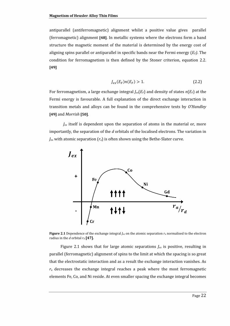
Jex with atomic separation (ra) is often shown using the Bethe-Slater curve.
Figure 2.1 Dependence of the exchange integral Jex on the atomic separation ra normalised to the electron
radius in the d orbital rd [47].
Figure 2.1 shows that for large atomic separations Jex is positive, resulting in
parallel (ferromagnetic) alignment of spins to the limit at which the spacing is so great
that the electrostatic interaction and as a result the exchange interaction vanishes. As
ra decreases the exchange integral reaches a peak where the most ferromagnetic
elements Fe, Co, and Ni reside. At even smaller spacing the exchange integral becomes

Magnetism of Heusler Alloy Thin Films
Page 23
negative and antiferromagnetic order dominates. At extremely small spacing the
electrons can be regarded as having the same spatial co-ordinates. Here the Pauli
exclusion principle dominates forcing the spins to align antiparallel. At larger spacing
the electrons inhabit separate spatial co-ordinates but exhibit the same wave function
resulting in favourable parallel alignment [49]. This model correctly predicts the
magnetic properties for elements. However for alloyed systems such as Co-based
Heusler alloys this model must be extended to consider the hybridisation of orbitals
between different elements and how this affects the number of electrons that
contribute to the magnetic properties. Discussion of this extended model and its
relevance to Co-based Heusler alloys can be found in section 3.1.3.
2.1.2. Indirect Exchange
Indirect exchange coupling occurs when localised but separated magnetic moments in
metallic systems are coupled by conduction electrons. It was proposed and developed
by Ruderman and Kittel [51], Kasuya [52] and Yosida [53] to explain the coupling of
nuclear spins to s-electrons. This type of exchange interaction is often known as the
RKKY interaction.
This model has subsequently been used to describe the magnetic moments of
rare earth metals [54] as well as intergranular exchange coupling and the coupling
between magnetic layers separated by non-magnetic spacers [55]. When a localised
magnetic impurity is placed in a typical electron gas, that is a system of electrons free
from their ions which are treated as a non-interacting gas [56], the wave functions
change to accommodate the impurity. This effectively adds more possible states for
the conduction electrons when their spins are aligned with that of the magnetic
impurity. This also forms a series of charge oscillations. These oscillations are all in
phase at the impurity but as the electrons have different energies and therefore
wavelengths, these charge oscillations interfere at some distance from the impurity
[49]. These electrons all contain information about the initial spin state of the
magnetic impurity so these oscillations in charge are also oscillations in the spin
density. Therefore if a second localised magnetic moment is placed within the range of
these oscillations it will become coupled either ferromagnetically or
antiferromagnetically to the initial atom depending upon the spin density at its
position in the system [57].

Magnetism of Heusler Alloy Thin Films
Page 24
The dependence on the position of the coupled atoms makes this exchange
extremely susceptible to any change in the distance between local moments. This was
shown experimentally by Parkin et al. in a series of experiments using different
transition metal spacer layers of varying thickness to separate two ferromagnetic
layers [11,55,58]. Figure 2.2 shows clearly the oscillatory nature of the coupling of two
ferromagnetic layers on their separation. The strength and nature of the exchange
coupling is represented by the magnitude of the applied field at which the sample
saturates. Antiferromagnetic coupling requires a large field to saturate while
ferromagnetic coupling requires a lower saturating field.
Figure 2.2. The dependence of indirect exchange coupling on the thickness of a Cr interlayer separating
two ferromagnetic layers. The symbols represent three different films of the same structure. [55].
The other point to note about Figure 2.2 is the range over which the interaction
can take place. The coupling extends to a range of about 4 nm . This means that the
coupling can occur across grain boundaries making the RKKY interaction particularly
important in granular thin films. Individual grains can become exchange coupled and
reverse their magnetisation as if they were a single entity. This process is well
documented in thin film granular media [59]. This makes intergranular exchange an
important consideration when studying the polycrystalline Heusler alloy films in this
work.
Magnetism of Heusler Alloy Thin Films
Page 25
2.2. Magnetic Anisotropies
2.2.1. Magnetocrystalline Anisotropy
Anisotropy is the term used to describe the directional dependence of the properties
of a system. Magnetocrystalline anisotropy is the dependence of the ease of
magnetisation of a magnetic medium relative to the orientation of specific lattice
planes of the crystal. This results from the coupling of the local spin magnetic
moments to the shape and orientation of the electronic orbitals of the atoms in a
crystal. It is also controlled by the symmetry of the crystal field, or the electric field
created by the chemical bonding of atoms within the lattice [49]. This quenches the
direction of the orbitals along the crystal bonds. The electron spins align along these
orbitals, promoting a single or several preferential axes of spin alignment.
The result of this is one, or a set of, crystallographic directions (easy axes)
along which it is easier for magnetisation to align than other directions. The axis that
is hardest to magnetise is known as the hard axis. The crystallographic directions
away from the easy axes are harder to magnetise as aligning the spins requires the
breaking of the spin-orbit interaction. This requires energy expenditure from the
external field. When saturation is achieved along an axis other than an easy axis the
energy required to achieve this is stored in the crystal as the magnetocrystalline
anisotropy energy, EK. For the Heusler alloys studied in this thesis, the majority of the
spin (localised) contribution to the magnetisation comes from the Co atoms. These
exhibit octahedral symmetry, resulting in cubic-like magnetocrystalline anisotropy.
The anisotropy energy is given by equation 2.3:
( ) ( ) (2.3)
Where K0, K1 and K2 are the anisotropy constants for a given material and α1, α2 and α3
are the cosines of the angles made between the saturation direction and the [100],
[010], and [001] crystal axes respectively [47]. For a material with uniaxial anisotropy,
for example hcp Co where the easy axis lies along the c-axis, EK is given by [47]:
(2.4)
where θ is the angle between the easy axis and the magnetisation of the system. What
is evident from both equations is that the K0 term is independent of the angle, has no
Magnetism of Heusler Alloy Thin Films
Page 26
influence on the easy axis of magnetisation and therefore can be ignored. K1 is the
term of most importance as it is generally much larger than K2, thus we can generally
ignore K2. The sign of K1 and K2 can however be important, for positive K1 the easy axis
most likely lies along a cube edge (e.g. [100]). For materials with negative K1 (such as
Ni) the easy direction lies along the body diagonal (e.g. [111]) [57].
For Heusler alloy thin films the anisotropy constants are found to be greatly
system dependent, being affected by deposition technique as well as the substrate
onto which the film is deposited [46,60]. For single crystal films of Co2FeSi similar to
those characterised in this work the values of K1 have been measured in the range 1.8
to 4 x10⁴ ergs/cm3 [46]. The nature of the magnetocrystalline anisotropy itself is also
discussed and is found again to be heavily system dependent. Due to the L21 structure
being cubic it is expected that the magnetocrystalline anisotropy would be three-fold
cubic (see section 3.1.1 for details). However in experiments it is found that in the
single crystal films there is often an overlaid uniaxial anisotropy [46,61-63]. The origin
of this is not entirely understood. It has been hypothesised that this effective uniaxial
anisotropy arises from the substrate/film bonding [62] as previously reported for
Fe/GaAs [64].
2.2.2. Shape Anisotropy
In the polycrystalline films the dominant anisotropy is unlikely to be
magnetocrystalline. Shape anisotropy is more likely to be dominant. This arises from
the effect of the demagnetising field, Hd, if a magnetic grain is not spherical. If a grain is
elongated in any way then Hd along the short axis will be greater than Hd along the
long axis. A full description of the effect of shape on Hd and how this affects magnetic
anisotropy can be found in Cullity [47]. In essence, the quantitative treatment uses the
magnetostatic energy of the grain, Ems, and how this changes with the direction of an
applied field relative to the magnetisation, M, equation 2.5.
(2.5)
Nd is the shape demagnetising factor which expresses how the demagnetising field
changes with grain shape, . The example case that will be most applicable
to the specimens in a film is a prolate spheroid. This is shown in Figure 2.3 with a
major axis c and a minor axis a magnetised to M at an angle θ to the major axis.

Magnetism of Heusler Alloy Thin Films
Page 27
Figure 2.3. Magnetised prolate spheroid.
The condition depicted in Figure 2.3 is considered in terms of equation 2.5
when the axis dependent shape demagnetising factors Nc and Na for Ems are defined.
The term for the second factor is angle dependent and takes exactly the same form as
that for K1 in the uniaxial case (equation 2.4). It is possible to express the shape
anisotropy constant Ks as
( )
(2.6)
Equation 2.6 shows that the magnitude of the shape anisotropy is a function of both
the axial ratio c/a as well as the magnetisation of a sample. For Co2FeSi at saturation,
Ms = 1140 emu/cm3. The variation in the shape anisotropy with the axial ratio of a
prolate spheroid has been calculated using the shape demagnetising factors from
reference [65] and the value of Ms above.
Figure 2.4. Variation of the shape anisotropy constant as a function of axial ratio for a prolate spheroid of Co2FeSi. The magnetocrystalline anisotropy K1 is shown by the red line.
It is shown in Figure 2.4 that this effect is quite significant. For single crystal
Co2FeSi the value of K1 is quoted as having a maximum of 4x10⁴ ergs/cm3 [46], which
is achieved through the shape anisotropy with an axial ratio of just 1.1. That is to say
that a prolate spheroid of Co2FeSi with no magnetocrystalline anisotropy and an axial

Magnetism of Heusler Alloy Thin Films
Page 28
ratio of 1.1 has the same uniaxial anisotropy as a spherical particle of Co2FeSi with the
measured uniaxial anisotropy as reported in reference [46]. More important in the
context of the polycrystalline films measured in this work is that a Co2FeSi grain with
an axial ratio of just 1.5 has shape anisotropy 4 times larger than the
magnetocrystalline anisotropy. This means that any elongation of Co2FeSi grains
means that shape anisotropy become the dominant term in the magnetisation reversal
process.
2.3. Magnetic Domains and Single Domain Particles
2.3.1. Domain Formation
Initially proposed by Weiss in 1906 domain theory is now central to understanding
the magnetisation processes in magnetic materials. Domains form to reduce the
magnetostatic energy of a magnetic material, the energy stored in the field which
attempts to demagnetise the sample. This process is shown schematically in Figure 2.5
for a material with strong uniaxial anisotropy (e.g. Co) [66].
Figure 2.5. Domain structure in a uniaxial single crystal [66].
The schematic shows that when a magnetic material is saturated in one
direction an opposing field is created, this is the demagnetising field HD which stores
the magnetostatic energy Ems (equation 2.5). The magnetostatic energy is dependent
primarily on the magnitude of the magnetisation of the sample. To reduce this
magnetisation, and therefore Ems, a magnetic material breaks into domains [66]. Each
domain contains magnetic moments aligned parallel to each other. Their magnetic
moments preferentially lie along the easy axes of the material. In the uniaxial material
in Figure 2.5, the domains form with magnetisation aligned anti-parallel along the
easy axis, reducing the demagnetising field and Ems. It is also possible for the material
Magnetism of Heusler Alloy Thin Films
Page 29
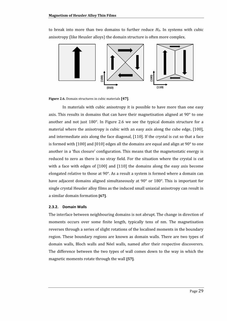
to break into more than two domains to further reduce HD. In systems with cubic
anisotropy (like Heusler alloys) the domain structure is often more complex.
Figure 2.6. Domain structures in cubic materials [47].
In materials with cubic anisotropy it is possible to have more than one easy
axis. This results in domains that can have their magnetisation aligned at 90° to one
another and not just 180°. In Figure 2.6 we see the typical domain structure for a
material where the anisotropy is cubic with an easy axis along the cube edge, [100],
and intermediate axis along the face diagonal, [110]. If the crystal is cut so that a face
is formed with [100] and [010] edges all the domains are equal and align at 90° to one
another in a ‘flux closure’ configuration. This means that the magnetostatic energy is
reduced to zero as there is no stray field. For the situation where the crystal is cut
with a face with edges of [100] and [110] the domains along the easy axis become
elongated relative to those at 90°. As a result a system is formed where a domain can
have adjacent domains aligned simultaneously at 90° or 180°. This is important for
single crystal Heusler alloy films as the induced small uniaxial anisotropy can result in
a similar domain formation [67].
2.3.2. Domain Walls
The interface between neighbouring domains is not abrupt. The change in direction of
moments occurs over some finite length, typically tens of nm. The magnetisation
reverses through a series of slight rotations of the localised moments in the boundary
region. These boundary regions are known as domain walls. There are two types of
domain walls, Bloch walls and Néel walls, named after their respective discoverers.
The difference between the two types of wall comes down to the way in which the
magnetic moments rotate through the wall [57].

Magnetism of Heusler Alloy Thin Films
Page 30
As shown in Figure 2.7, Bloch walls change the direction of the magnetisation
through confinement of the rotation of magnetic moments to the plane parallel to the
domain wall. Bloch walls occur when the magnetic moments rotate perpendicular to
the plane of the domain wall. Bloch walls occur in bulk samples. However, in thin films
they create free poles at the sample surface which contribute significant
magnetostatic energy to the system. To reduce this energy, Néel walls form which
rotate in the plane so that free poles don’t appear at the film surface [47].
Figure 2.7. Schematic diagrams of 180° a) Bloch and b) Néel domain walls.
Domain walls have a finite width, δ. The width of the domain wall results from
a balance of the anisotropy energy EK and exchange energy Eex in a magnetic material.
( ) (2.7)
where f is the function describing the anisotropy of the system, as per equations 2.3
and 2.4. ϕ is the angle that the magnetisation vector at a specific point in the wall
makes with the easy axis of the system.
(
)
(2.8)
where Aex is the exchange stiffness constant and x is the position of the moment within
the wall. Aex is a function of the exchange integral, the magnitude of the spin moment
and the number of spins per unit area of wall. The domain wall energy is the sum
equations 2.7 and 2.8, which when minimised, can give an expression for the effective
domain wall width, equation 2.9 [66].
√
(2.9)

Magnetism of Heusler Alloy Thin Films
Page 31
The width of the domain wall is thus controlled by the lowest energy state which is a
function of both the exchange coupling between spins in the wall and the anisotropy
constant of the system, whether that is cubic or uniaxial.
2.3.3. Formation of Single Domain Particles
If a magnetic material is not a single crystal and is instead made of fine particles or
grains then it is possible that some of these grains will only contain a single domain.
The phenomenological interpretation would suggest that if the width of the domain
wall is greater than the size of the grain then it is impossible to fit two domains and
the wall in the particle. More accurately this should be considered in terms of the
various energy contributions and how the energy in the grain would be minimised.
The magnetostatic energy will vary with the volume, D3, of the grain as Ems ∝ M2. The
domain wall energy will vary as a function of the grain cross section, D2 [47].
Therefore, at some point, there is a diameter of grain at which it becomes
energetically favourable for the grain to be in a single domain state. If a spherical
particle is taken as an example, then the critical radius, rc, at which the single domain
state becomes favourable is given by [49]:
( )
⁄
(2.10)
Equation 2.10 is an approximation and only holds in the limit of large values of K.
O’Handley [49] gives an extensive discussion of the effect of grain parameters on the
critical radius for single domain particle behaviour. This single domain behaviour and
the limiting cases are extremely important for the evaluation of the polycrystalline
films studied in this work. In polycrystalline films the grain size is distributed. As such
it is possible for there to be both single and polydomain particles in the film. This can
have a large effect on the magnetisation reversal mechanism in these films.
2.4. Magnetisation Reversal Processes
2.4.1. Domain Wall Motion
When an external field is applied to a magnetic material the domains aligned with the
field will grow. If the material is initially saturated, a field applied opposite to this
saturation direction will nucleate a domain with its magnetisation aligned with the
field. This nucleation occurs through the rotation of a small number of moments in the
film. Magnetisation reversal through rotation will be discussed in section 2.4.3. If a
Magnetism of Heusler Alloy Thin Films
Page 32
sufficiently large field is applied, the material will saturate in the direction of the
applied field. The growth of domains requires the motion of the domain walls. This
motion is not smooth and the domain walls move through a series of jerky steps
known as Barkhausen jumps [47]. These jumps are the result of continuous pinning
and de-pinning of the domain wall as it moves through the material. The domain wall
must move through an energy landscape with a series of peaks and troughs. The peaks
in this landscape are pinning sites where the domain wall requires extra energy to
overcome this pinning energy, usually in the form of an applied field. This is shown
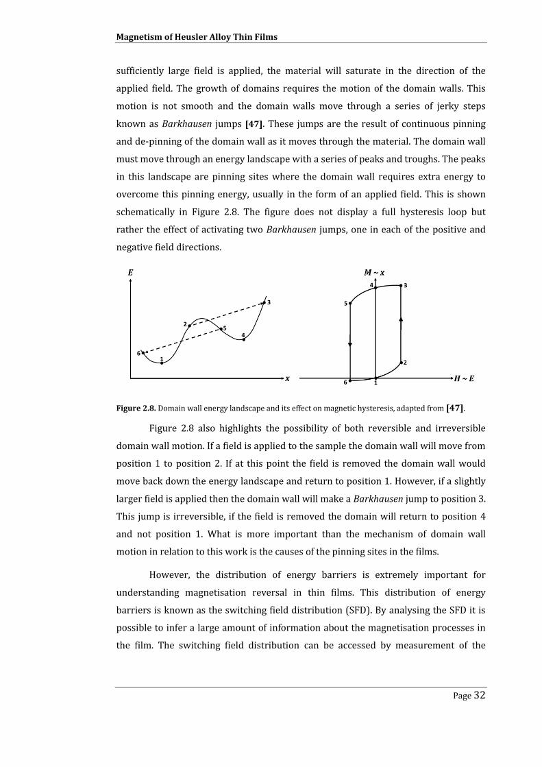
schematically in Figure 2.8. The figure does not display a full hysteresis loop but
rather the effect of activating two Barkhausen jumps, one in each of the positive and
negative field directions.
Figure 2.8. Domain wall energy landscape and its effect on magnetic hysteresis, adapted from [47].
Figure 2.8 also highlights the possibility of both reversible and irreversible
domain wall motion. If a field is applied to the sample the domain wall will move from
position 1 to position 2. If at this point the field is removed the domain wall would
move back down the energy landscape and return to position 1. However, if a slightly
larger field is applied then the domain wall will make a Barkhausen jump to position 3.
This jump is irreversible, if the field is removed the domain will return to position 4
and not position 1. What is more important than the mechanism of domain wall
motion in relation to this work is the causes of the pinning sites in the films.
However, the distribution of energy barriers is extremely important for
understanding magnetisation reversal in thin films. This distribution of energy
barriers is known as the switching field distribution (SFD). By analysing the SFD it is
possible to infer a large amount of information about the magnetisation processes in
the film. The switching field distribution can be accessed by measurement of the
Magnetism of Heusler Alloy Thin Films
Page 33
irreversible susceptibility χirr. This is found from the differential of the DC
Demagnetised (DCD) remanence curve which will be discussed in greater detail in
chapter 5. The irreversible susceptibility is a measurement of purely the irreversible
components of the reversal process, such as Barkhausen jumps or in granular films the
rotation of magnetisation through the grain.
2.4.2. Hindrances to Domain Wall Motion
The motion of a domain wall requires an energy input, therefore any regions of the
film that increase this energy cost act as domain wall pins. Possible causes of these
energy increases include inclusions, surface roughness and microstresses within the
material. A comprehensive discussion of the many possible hindrances to domain wall
motion can be found in Cullity [47]. Here there is only an overview of those hindrances
relevant to this work.
Inclusions are areas of the film that have a different magnetisation than the
surrounding material. Essentially, inclusions moderate the exchange interaction
between moments in the wall, increasing the energy. These inclusions can take many
forms. Different phases of an alloy or impurities in the magnetic material are most
relevant to the work in this thesis. Vacancies in the lattice can also act as inclusions. As
Heusler alloys can exhibit many different disordered phases, the effect of these
different phases of the alloy on the magnetic properties is extremely important.
However, as well as hindering domain wall motion, these disordered phases can also
aid domain wall motion. This is due to reduced magnetocrystalline anisotropy when
compared to that of the perfect L21 Heusler structure. A number of the films in this
work are multilayers. Interatomic diffusion between the layers can lead to a build-up
of impurities in the magnetic layers, which can also act as hindrances to domain wall
motion.
Surface roughness can lead to significant domain wall pinning. A domain wall
will always try to reduce its own energy. Surface roughness allows this through
reduction of the domain wall area in the thinner regions of the film. Therefore the
domain walls will always pin in the valleys of the film. The final hindrance to domain
wall motion that is considered here is the effect of microstress. Microstresses arise
from the deformation of lattice planes within the material. This can have a number of
origins although the most common of these are the effects of defects and dislocations.
Microstress hinders domain wall motion as it alters the local anisotropy field through
Magnetism of Heusler Alloy Thin Films
Page 34
a stress anisotropy. This extra anisotropy increases the energy the domain wall has to
overcome to move beyond that point, thus pinning the wall. In epitaxially sputtered
films these microstresses are of particular importance as the lattice match between
most Co-Based Heusler alloys and substrates is not perfect. As a result, misfit
dislocations form at these interfaces to relieve the stress as much as possible. This
does not completely remove the stresses and these dislocations will still deform the
local lattice planes. This can contribute a significant localised stress anisotropy to the
film.
2.4.3. Magnetisation Rotation
It is also possible to change the magnetisation of a magnetic material by rotation of
the moments through the material. This happens to a small extent in domain wall
controlled systems but is most commonly examined in terms of single domain
particles. For domain wall systems this is usually the highest energy part of the
hysteresis loop which occurs when the bulk of the film has already reversed its
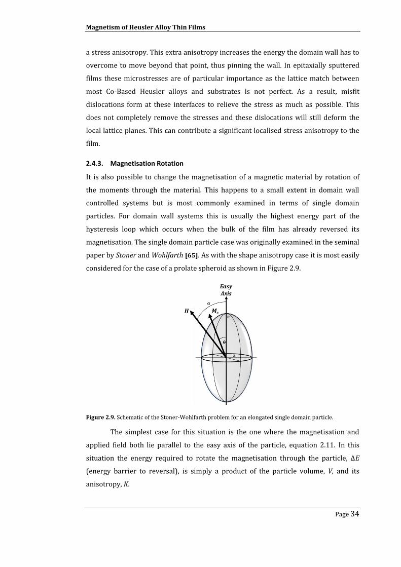
magnetisation. The single domain particle case was originally examined in the seminal
paper by Stoner and Wohlfarth [65]. As with the shape anisotropy case it is most easily
considered for the case of a prolate spheroid as shown in Figure 2.9.
Figure 2.9. Schematic of the Stoner-Wohlfarth problem for an elongated single domain particle.
The simplest case for this situation is the one where the magnetisation and
applied field both lie parallel to the easy axis of the particle, equation 2.11. In this
situation the energy required to rotate the magnetisation through the particle, ΔE
(energy barrier to reversal), is simply a product of the particle volume, V, and its
anisotropy, K.

Magnetism of Heusler Alloy Thin Films
Page 35
(2.11)
The result of this is that the energy of the applied field needed to saturate the particle
is exactly equal to the anisotropy energy. This energy is often expressed in terms of an
anisotropy field HK at T = 0 K.
If the applied field is not aligned with the magnetisation then the energy
barrier to reversal is reduced. This reduction is proportional to the angle between the
easy axis and M. Therefore, the energy required to reverse the magnetisation in the
non-aligned case is a sum of the reduced energy barrier and the energy from the
applied field, equation 2.12.
( ( )) (2.12)
The effect of an applied field angle on the hysteresis of the particle can be seen
in Figure 2.10. The figure shows that for the aligned case the hysteresis loop is square
with the magnetisation reversal taking place at HK. As the applied field angle increases
both the remanent moment and the coercivity decrease.
Figure 2.10. Hysteresis loops for prolate spheroids with a field applied at an angle α to the easy axis
[65].
This type of single particle behaviour is important for a number of films in this
work. However it must be noted that the results of Figure 2.10 only hold at T = 0 K.
This result does however give an excellent basic understanding of the magnetic
properties of single domain particle systems. Importantly, the decrease of both Mr and
Magnetism of Heusler Alloy Thin Films
Page 36
Hc when the particle is misaligned with the field is demonstrated. This is likely to be
the case for the polycrystalline films in this work, where due to the sputtering process
parameters α is likely to be distributed, as are both V and K.
The Stoner-Wohlfarth model makes a number of assumptions that are not true
for many real systems, primarily that the spins in the material all remain parallel
(coherent) whilst rotating. This is not always the case, a number of different models
have been proposed for systems that do not show Stoner-Wohlfarth behaviour. The
two most often observed incoherent modes of rotation are spin fanning and curling.
Spin fanning occurs when an elongated particle essentially breaks into smaller
magnetic entities which reverse out of phase with one another, often called the chain
of spheres model. In the spin curling model the spins ‘curl’ through the particle always
remaining perpendicular to the radius. As a result, the spins are no longer coherent
with one another. Both these mechanisms are most commonly seen in extremely
elongated particles. As a result, it is unlikely that these two reversal mechanism will
be observed in this work. A full description of both processes can be found in the
standard text [47].
2.5. Magnetic Activation Volumes
2.5.1. Magnetic Viscosity
The Stoner-Wohlfarth model only applies at T=0 K. Above this temperature thermal
energy excites fluctuations in the magnetisation of a sample. These fluctuations can
have amplitude sufficient to reverse regions of a thin film. The characteristic time (τ)
that it takes for a magnetic system to lose 37% of its magnetisation due to thermal
activation is described by equation 2.13, an Arrehnius law formalised by Néel [68].
( ( ⁄ )
)
(2.13)
fo is the attempt frequency which is often given the value 109 Hz [69]. In real thin films
the volume of grains is distributed. This leads to a distribution of the energy barriers
to reversal. It was found that when the distribution is wide the decay of magnetisation
follows a ln(t) law [70]:
( ) ( ) ( ⁄ ) (2.14)

Magnetism of Heusler Alloy Thin Films
Page 37
where S is the coefficient of magnetic viscosity. The sign of the second term is
dependent upon whether the magnetisation is deemed to be positive or negative in
the initial state. Equation 2.14 is however the 1st order approximation to a series
expansion in ln(t) which can describe the magnetisation decay in any system.
Equation 2.14 is sufficient to describe a system with a wide energy barrier
distribution ΔE, whose magnetisation varies linearly in ln(t) such as those found in
this work. In systems with distributed energy barriers, S must also be distributed as it
is intrinsically linked as shown by Gaunt through equation 2.15 [71].
( ) ( ( )) (2.15)
where ΔE(H) describes the energy barrier distribution being activated at a specific
applied field. S(H) goes through a maximum at Hc. The coefficients of magnetic
viscosity at different field values can be determined experimentally by measuring a
series of magnetic time dependence curves through the method described fully in
section 5.1.3.
2.5.2. The Fluctuation Field and the Activation Volume
The idea of the fluctuation field (Hf) was initially proposed by Néel in 1951 [72]. Hf is a
fictitious field which is used to couple the effect of thermal energy to a magnetic
system. This extended the ideas of Street [70] . The fluctuation field, equation 2.16,
was considered in more detail by Wohlfarth [73] to understand the observed time
dependence of magnetisation. The constant of proportionality originally used by Néel
was found to have the dimensions of magnetic moment given by MsVact, where Vact is
known as the activation volume of reversal.
(2.16)
For the work in this thesis it is more useful to write this equation in terms of
the activation volume as this is often the parameter to be found. Thus the parameters
to be measured are the fluctuation field and saturation magnetisation at the
measurement temperature. Hf may be determined experimentally through
measurement of the magnetic viscosity coefficients, as well as the irreversible
susceptibility χirr(H) via equation 2.17 as initially proposed by Street et al. [74]. χirr(H)
Magnetism of Heusler Alloy Thin Films
Page 38
can be determined from the differential of a DCD remanence curve as described in
section 5.1.3.
( ) ( )
( )
(2.17)
This determination of the fluctuation field is limited to systems where the
energy barrier distribution is sufficiently wide as to allow linear decay of M with ln(t).
For systems with a narrow energy barrier distribution another formulation of Hf was
proposed by El-Hilo et al. equation 2.18 [75]. This uses the difference in time for
achieving the same value of M at different applied fields.
( ⁄ ) |
(2.18)
A full description of the derivation of this form of Hf can be found in reference [75] but
this will not be reproduced here as the films in this work can all be analysed using the
linear case, equation 2.17 due to them having a sufficiently wide distribution of energy
barriers.
2.5.3. The Activation Volume in Heusler Alloy Thin Films
As the fluctuation field is a fictitious field the activation volume in not a real volume in
the film. It can however give a lot of information about the magnetisation reversal
processes in a thin film. It has been used widely in magnetic recording media to
understand the size of bits [76], where a number of grains may reverse their
magnetisation co-operatively. By applying this technique to Heusler alloy films it is
possible to understand how the reversal mechanisms may affect possible spintronic
devices.
In granular polycrystalline films, the activation volume may be representative
of the magnetisation reversal of a single magnetic grain, multiple magnetic grains or in
certain cases a fraction of a single magnetic grain [77]. In single crystal or epitaxial
films that reverse via domain wall motion the activation volume is analogous to the
volume swept out by a single Barkhausen jump. The size of these reversal events is of
particular importance to nanoscale spintronic devices, such as a magnetoresistive
nanopillar. It is important to understand what fraction of a magnetic nanopillar will
reverse coherently during operation as this can have a large effect on the signal from
the device, especially at high frequency.
Co-Based Heusler Alloys
Page 39
Chapter 3. Co-Based Heusler Alloys
Heusler alloys are an unusual class of materials which number over 3000 compounds
and can comprise of almost every element in the periodic table. These compounds can
have a wide range of properties from being half-metals [29], semiconductors [78]
superconductors [79], topological insulators [80] and many more besides. These
remarkable compounds were initially discovered by Fritz Heusler in 1903 whilst
studying the ferromagnetism of an alloy with composition Cu2MnAl [81]. Heusler
alloys are generally ternary compounds although a number of quaternary compounds
such as Co2Fe(Al,Si) [19,82] and Co2(Cr,Fe)Al [83] are being studied for spintronic
applications. These compounds are usually split into two groups, those with 1:1:1
(Half-Heusler) stoichiometry and those with 2:1:1 (Full-Heusler) stoichiometry. Co-
based full-Heusler alloys are of particular interest for spintronic applications as they
can exhibit half metallic properties above room temperature. These materials also
have high Curie temperatures as well as good lattice matches with widely used III-V
semiconductors and MgO substrates [84].
3.1. The Heusler Structure and the Origins of Magnetism
3.1.1. Crystal Structure and Disordered Phases
Full Heusler alloys with 2:1:1 stoichiometry, often referred to as X2YZ, crystallise in
the cubic L21 structure, where the X and Y are transition metals and the Z is a main
group element. This structure is formed of four interpenetrating fcc sublattices. Two
sublattices are equally occupied by the X element of the compound and the other two
are occupied by the Y and Z elements. The result of this is a rocksalt type structure
formed from the Y and Z elements filling the octahedral positions of the lattice, whilst
the atoms of the X element fill the vacant tetrahedral positions. The structure has also

Co-Based Heusler Alloys
Page 40
been described in terms of a zinc-blende type structure or a superlattice of the CsCl-
like structure [84]. The L21 structure is shown in Figure 3.1.
Figure 3.1. Types of order and disorder occurring in Heusler structures, a) L21 b) B2 c) DO3 and d) A2.
The magnetic and half-metallic properties of Heusler alloys are strongly dependent on
the atomic ordering. It is therefore always important, if not essential, to characterise
the crystal structure of the material. There are a number of common disordered
phases which vary from the L21 Heusler structure. The effect of these disordered
phases will be discussed in more detail later in this chapter. If the Y and Z sites
become interstitially disordered the B2 structure is formed as shown in Figure 3.1.
Disorder between the X and Y sites can also occur which forms the DO3 structure. This
structure can however be the highest ordered phase of certain intermetallic alloys
with Heusler like structure (X = Y) such as Fe3Si [85]. Disorder can also occur among
all atom sites resulting in the totally disordered A2 structure.
3.1.2. The Origin of Half Metallicity
The origin of half-metallicity in full-Heusler alloys was initially described by Galanakis
et al. [86] for the compound Co2MnGe. In the Galanakis interpretation the lattice is
initially treated as just the Co2 positions so the hybridisation of d-orbitals for the
minority states in Co-Co interactions are calculated first. These are shown in Figure

Co-Based Heusler Alloys
Page 41
3.2a. In the figure, d1 to d5 correspond to the and the
orbitals, respectively. The differences between these orbitals are also shown in Figure
3.2a. Between two neighbouring Co atoms in the lattice two hybridised orbitals form
from the d4 and d5 orbitals, forming a low energy bonding eg orbital and a high energy
eu antibonding orbital. The d1, d2 and d3 orbitals hybridise to form a triply degenerate
low energy bonding t2g orbital and a triply degenerate high energy antibonding t1u
orbital. Where t1u, t2g, eg and eu are the chemical nomenclature describing the shape
(angular momentum) of the hybrid orbital.
Figure 3.2. Possible hybridisation between d orbitals for minority states for the compound Co2MnGe by
considering a) the Co-Co interaction and b) the Mn-(Co-Co) interaction [86]. The shapes of the different d orbitals are also shown in a).
The contribution from the Mn atoms in the lattice must also be considered as
well as the Co-Co interaction. The d-orbitals from the Mn atoms hybridise in a similar
way to that seen for Co-Co. Figure 3.2b shows that the d4 and d5 orbitals hybridise
with the double degenerate eg orbital of the Co-Co to form two eg orbitals, one low
energy bonded and one high energy antibonded orbital. The d1, d2, and d3 orbitals
also hybridise with the triple degenerate t2g orbital from the Co-Co to form 6 more t2g
orbitals, three of which are bonding and sit below the Fermi energy and another three
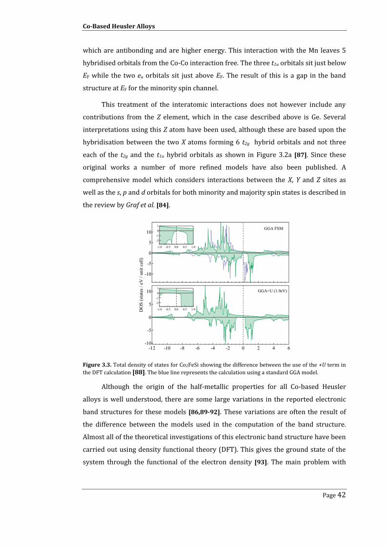
Co-Based Heusler Alloys
Page 42
which are antibonding and are higher energy. This interaction with the Mn leaves 5
hybridised orbitals from the Co-Co interaction free. The three t1u orbitals sit just below
EF while the two eu orbitals sit just above EF. The result of this is a gap in the band
structure at EF for the minority spin channel.
This treatment of the interatomic interactions does not however include any
contributions from the Z element, which in the case described above is Ge. Several
interpretations using this Z atom have been used, although these are based upon the
hybridisation between the two X atoms forming 6 t2g hybrid orbitals and not three
each of the t2g and the t1u hybrid orbitals as shown in Figure 3.2a [87]. Since these
original works a number of more refined models have also been published. A
comprehensive model which considers interactions between the X, Y and Z sites as
well as the s, p and d orbitals for both minority and majority spin states is described in
the review by Graf et al. [84].
Figure 3.3. Total density of states for Co2FeSi showing the difference between the use of the +U term in
the DFT calculation [88]. The blue line represents the calculation using a standard GGA model.
Although the origin of the half-metallic properties for all Co-based Heusler
alloys is well understood, there are some large variations in the reported electronic
band structures for these models [86,89-92]. These variations are often the result of
the difference between the models used in the computation of the band structure.
Almost all of the theoretical investigations of this electronic band structure have been
carried out using density functional theory (DFT). This gives the ground state of the
system through the functional of the electron density [93]. The main problem with
Co-Based Heusler Alloys
Page 43
calculations performed using this method is that the calculation uses the ground state
of the system so that all calculations must be made at T= 0 K, which is unrealistic for
most experimental measurements. The other main downfall of DFT is that the
potentials describing the interactions between electrons are not realistic. This means
that certain approximations must be made. One of these assumptions is that the
valance electrons are itinerant. However, for Heusler alloys this is not true, as the
valence electrons can become strongly localised to the Co d orbitals [86]. Therefore,
additional correction terms must be made to account for this, such as an electron-
electron correlation term, often called the +U term [30,89], the effect of which can be
seen in Figure 3.3.
The densities of states shown in Figure 3.3 have been calculated using the
generalised gradient approximation (GGA) for the energy density. This is a more
accurate approximation than the widely used local density approximation (LDA) as it
uses terms for both the energy density and the gradient of the energy density at a
specific point. The +U term is the DFT formulation of the Hubbard model U term which
describes the electron repulsion term effectively splitting localised d or f electrons
from the itinerant background [94]. The difference in the effect of this term is clear as
it not only changes the position of the Fermi energy in the band gap but also the shape
of the density of states around the minority spin band gap [88].
3.1.3. Generalised Slater Pauling Behaviour in Heusler Alloys
Slater [95] and Pauling [96] both studied the origin of ferromagnetism from the band
theory of transition metals, observing that ferromagnetism in these compounds
results from the intrinsic properties of the bands formed from the 3d orbitals. They
discovered that the magnetic moment of a 3d metal (and also its binary alloys) can be
estimated through the average number of valence electrons (Nv) available per atom.
This results in the curve seen in Figure 3.4, where a peak occurs between Nv = 8 and
Nv = 9 where Fe sits. Below Nv = 8 the magnetism is the result of localised electrons
and these elements would typically exhibit bcc-like structures. Above Nv = 9 the
magnetism is the result of itinerant electrons and the crystal structures are typically
close packed [97]. The Co-based Heusler alloys are found in the former ‘localised’
region of the curve. Although the L21 structure is comprised of 4 fcc lattices, the result
is in effect a supercell made up of 8 bcc CsCl-like unit cells. In this region of the curve
the Slater-Pauling rule can be approximated to [90],

Co-Based Heusler Alloys
Page 44
(3.1)
However, for half metallic ferromagnets, the band gap for the minority states requires
that the number of filled minority states be an integer. For the rule as approximated
above, the number of minority states may be non-integer if the value of the average
number of valence electrons is not an integer value. For these compounds, it is better
to generalise the number of valence electrons per atom to the average number of
valence electrons per formula unit Nf.u. so that for a full Heusler alloy with X2YZ
structure equation 3.1 becomes [90]
(3.2)
This generalised Slater-Pauling rule, equation 3.2, has also been found to hold for
quaternary compounds such as Co2Fe(Al,Si) [84].
Figure 3.4. The dependence of the magnetic moment for 3d elements and compounds on the average
number of valence electrons per formula unit showing the Slater-Pauling relationship [84].
Figure 3.4 also shows that the magnetic moments in Heusler compounds can be
controlled by the valance of the Z atom in the structure. It is clear to see that the
compounds where the Z atom has 4 valence electrons, in this case Si, have a higher
moment than an equivalent compound with 3 valance electrons (Al and Ga). This
unusual behaviour is a result of an increased number of d electrons in the bands
resulting from these Z atoms. This is extremely important for the development of new
Heusler compounds as it means that the alloy can be engineered to provide specific
magnetic characteristics.

Co-Based Heusler Alloys
Page 45
The agreement with the Slater-Pauling curve and the dependence of magnetic
moment on the valence electrons opens up the ability to engineer the properties of
Heusler alloys continuously. By substituting varying amounts of the constituent atoms
it is possible to change both the magnetic moment as well as the band structure. This
technique has been used to engineer quaternary compounds such as Co2FeAlxSi1-x
[39,98] and Co2FexMn1-xSi [99] that show a significant improvement in half-metallic
properties. In fact the properties have been improved to such an extent that the
highest ever published value of TMR (832% at 9K) was acquired using an MTJ with
Co2FeAl0.5Si0.5 electrodes [34].
3.2. The Effects of Structural Disorder in Heusler Alloys
3.2.1. Magnetic Properties
Any variation away from Heusler stoichiometry or changes in the Heusler structure
can have a large effect on the magnetic properties of the compound. In the previous
section it was shown that the magnetism in the Heusler alloys is the result of the
complex hybridisation of the atomic orbitals in the compound. As a direct result of
this, any atomic swaps change this local hybridisation and as a result the band
structure of the compound. Because the magnetic moments in Heusler compounds
come from spin moments of valance electrons localised to the d orbitals of the Co
atoms, any changes to the interatomic spacing also has a large effect on this
localisation. In other words, any changes to the lattice constant in these materials can
also have a dramatic effect on the magnetism. Because of the large variety of Heusler
compounds it is impossible to describe how disorder affects all Co-based Heusler
alloys. Therefore, Co2FeSi will be the focus of this discussion due to it being the
material of choice for experiments in this work.
Firstly, we consider the effect of disorder in the Heusler structure. The
possible atomic swaps that disorder the L21 crystal can be reduced to Fe-Si (B2
disorder), Co-Fe (DO3 disorder) and Co-Fe-Si (A2 disorder). The fully ordered L21 unit
cell should result in a moment of 6 μB/f.u. In cgs units this equates to 1140 emu/cm3
[89]. The effect of these atomic swaps has been calculated by Li et al. [100] using DFT.
Their model predicts that Co-Fe swaps reduce the moment per formula unit to 5.5 μB
with just 10% atomic disorder. The Co-Si swaps with the same amount of disorder are
surprisingly predicted to result in an increase in the moment to 6.05 μB/f.u. This is due

Co-Based Heusler Alloys
Page 46
to the resulting environment of the Co atom changing the symmetry of the interatomic
bonds and promoting an increased atomic moment for the Co site. The Fe-Si swaps
forming B2 disordered structures were found to retain the 6 μB moment predicted for
the L21 structure up to 10% disorder. This is however contrary to a number of
experimental studies which show a decrease in magnetic moment with increasing B2
ordering [90,101,102]. This is most likely due to the effect of widespread disordered
regions in the materials and not to just atomic swapping localised to the unit cell.
Variation in the lattice parameter of Co2FeSi has also been shown to affect the
magnetic moment. The lattice parameter of bulk Co2FeSi is reported to be 5.64Å
[90,103]. However, in thin films, the lattice parameter has been shown to expand and
contract dependent upon the growth mechanism and factor such as choice of
substrate and buffer layers [104]. These variations in lattice parameter can either
increase or decrease the intensity of the magnetic moment. Compression of the lattice
parameter by 6% has been shown to give a reduction of the magnetic moment from
the bulk value of 6 μB to 5 μB [89]. However, an increase in the lattice parameter of up
to 10% is shown to provide only small variations ±0.15 μB [89]. These variations in
magnetic properties are small when compared with the effect that structural variation
and disorder have on the half-metallicity and, as a result, spin polarisation of these
materials.
3.2.2. Half-Metallicity
The effect of disorder on the half-metallic nature of Heusler alloys is
considerably larger than that induced by lattice changes. This is due to the sensitivity
of the band gap for minority spin states to changes in the hybridisation of atomic
orbitals due to changes in atomic positions [105,106]. In the experimental results it is
extremely hard to quantify the effect of different types of disorder as they are often
randomly distributed throughout a system, as well as being specific to the particular
experiment. To give some understanding a number of atomic swap type disorders are
considered in the literature. Fe-Si (B2) and Co-Fe-Si (A2) [91] disorders are most
widely studied with some consideration for Co-Fe (DO3) [107]. Unfortunately the
models used to calculate the extent of disorder are often limited by the size of the
initial unit cell considered. For example, one on the most extensive studies on the
effect of disorder in Co2FeSi-based alloys by Gercsi and Hono [91] only used a sixteen
atom unit cell, which limits the minimum amount of disorder to 25% for B2 type and

Co-Based Heusler Alloys
Page 47
12.5% for the A2 and DO3 types. However, this is enough to acquire some
understanding of how these disorders affect the half-metallicity.
Figure 3.5. Variation in the spin dependent density of states for Co2FeSi with different quantities of a) B2,
b) DO3 and c) A2 disorder. The L21 spin density of states is shown in grey as a reference [91].
As can be seen in Figure 3.5, the different disorders affect the density of states
in different ways. The B2 type disorder is seen to retain the minority state band gap
and as a result the half-metallic conduction properties even at 25% disorder. This
maintenance of the band gap for the B2 ordering is because of the lack of the disorder
to the Co-Co symmetry in the lattice. It has been shown that the band gap is
constructed of 3d states localised to the Co atoms [108]. Therefore, if these states are
not altered by the disorder, the half-metallic electronic properties should remain. For
the DO3 disorder, the band gap is reduced and moves relative to EF, producing a small
but finite number of states for the minority channel at EF. However with, the A2
disorder the band gap is completely destroyed and there is an increase in states for
the minority channel resulting in a small inverse spin polarisation. The inversion of
spin polarisation has been identified experimentally [109].
As with the magnetic moment, the size of the unit cell can have an effect on the
calculation of the spin polarisation. This effect is especially prevalent in DFT
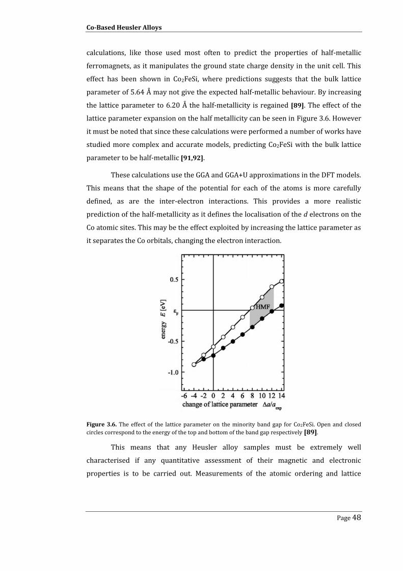
Co-Based Heusler Alloys
Page 48
calculations, like those used most often to predict the properties of half-metallic
ferromagnets, as it manipulates the ground state charge density in the unit cell. This
effect has been shown in Co2FeSi, where predictions suggests that the bulk lattice
parameter of 5.64 Å may not give the expected half-metallic behaviour. By increasing
the lattice parameter to 6.20 Å the half-metallicity is regained [89]. The effect of the
lattice parameter expansion on the half metallicity can be seen in Figure 3.6. However
it must be noted that since these calculations were performed a number of works have
studied more complex and accurate models, predicting Co2FeSi with the bulk lattice
parameter to be half-metallic [91,92].
These calculations use the GGA and GGA+U approximations in the DFT models.
This means that the shape of the potential for each of the atoms is more carefully
defined, as are the inter-electron interactions. This provides a more realistic
prediction of the half-metallicity as it defines the localisation of the d electrons on the
Co atomic sites. This may be the effect exploited by increasing the lattice parameter as
it separates the Co orbitals, changing the electron interaction.
Figure 3.6. The effect of the lattice parameter on the minority band gap for Co2FeSi. Open and closed
circles correspond to the energy of the top and bottom of the band gap respectively [89].
This means that any Heusler alloy samples must be extremely well
characterised if any quantitative assessment of their magnetic and electronic
properties is to be carried out. Measurements of the atomic ordering and lattice
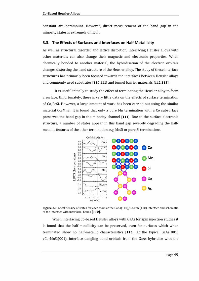
Co-Based Heusler Alloys
Page 49
constant are paramount. However, direct measurement of the band gap in the
minority states is extremely difficult.
3.3. The Effects of Surfaces and Interfaces on Half Metallicity
As well as structural disorder and lattice distortion, interfacing Heusler alloys with
other materials can also change their magnetic and electronic properties. When
chemically bonded to another material, the hybridisation of the electron orbitals
changes distorting the band structure of the Heusler alloy. The study of these interface
structures has primarily been focused towards the interfaces between Heusler alloys
and commonly used substrates [110,111] and tunnel barrier materials [112,113].
It is useful initially to study the effect of terminating the Heusler alloy to form
a surface. Unfortunately, there is very little data on the effects of surface termination
of Co2FeSi. However, a large amount of work has been carried out using the similar
material Co2MnSi. It is found that only a pure Mn termination with a Co subsurface
preserves the band gap in the minority channel [114]. Due to the surface electronic
structure, a number of states appear in this band gap severely degrading the half-
metallic features of the other termination, e.g. MnSi or pure Si terminations.
Figure 3.7. Local density of states for each atom at the GaAs(110)/Co2FeSi(110) interface and schematic
of the interface with interfacial bonds [110].
When interfacing Co-based Heusler alloys with GaAs for spin injection studies it
is found that the half-metallicity can be preserved, even for surfaces which when
terminated show no half-metallic characteristics [115]. At the typical GaAs(001)
/Co2MnSi(001), interface dangling bond orbitals from the GaAs hybridise with the

Co-Based Heusler Alloys
Page 50
Heusler alloy and create interfacial states at the Fermi energy thus destroying the
half-metallicity. If the interface is constructed of two (110) surfaces the orbitals in the
Heusler alloy hybridise in such a way as to force the GaAs localised state away from EF
thus preserving the half-metallicity. This interface also has no Co-As bonds which
contribute localised states at the Fermi energy. The GaAs/Co2MnSi interface and the
local density of states for each atom are shown in Figure 3.7. The properties of the
interface between Co-based Heusler alloys and insulating materials such as MgO or
AlOx are again different. These interfaces are extremely important as they can control
the maximum achievable value of TMR for a magnetic tunnel junction, as well as the
temperature dependence of that value [115]. Extremely high values of TMR (>500%)
have been measured for systems with AlOx [116] but this can be improved by using
crystalline MgO barriers.
By using a crystalline MgO barrier the coherent tunnelling effect can be
exploited. This was initially observed in Fe/MgO/Fe(001) junctions [117] after being
theoretically predicted by Butler et al. [23]. Coherent tunnelling occurs when the
electron wavefunction remains coherent through the entire junction. This means that
the same electron band symmetry is preserved though the entire junction. In
Fe/MgO/Fe(001) junctions this occurs for the Δ1 band in the majority spins states but
not for the minority states resulting in a prediction of half-metallic conduction [23].
The same situation arises for Co-based Heusler alloy MTJ’s with crystalline MgO
barriers [115]. Once again taking Co2MnSi as the example, it was found that the
interfacial bonding can also result in the creation of interfacial states in the minority
band gap. This effectively destroys the half metallicity and therefore spin polarisation
of the electrode, therefore reducing the maximum TMR ratio if considered in terms of
the initial Julliere model, equation 3.3 [20]. P1 and P2 are the value of spin polarisation
for the top and bottom electrodes respectively.
(3.3)
As well as being affected by the reduction of spin polarisation of the electrodes
the TMR ratio in these films also shows large temperature dependence. This has been
suggested to result from an increased contribution from the interfacial states at higher
temperature. At low temperature there are relatively few spin-flip transitions which
allow conduction from the minority band. However, at higher temperatures the

Co-Based Heusler Alloys
Page 51
probability of these spin-flip transitions increases. This increases the contribution to
the conductance from electrons in the minority states resulting in a further and
accelerated decrease in the TMR value with increasing temperature [118]. The same
temperature dependence is not seen in MTJ’s with typical ferromagnetic (Fe or
CoFeB) electrodes [119].
3.4. Experimental Observations of Heusler Alloy Spin Polarisation
Many observations have been made of large spin polarisation in spintronic devices
using Co-based Heusler alloy ferromagnetic layers. The devices primarily fall into the
categories of MTJ’s [34,82] or spin valves [19,41], although some devices such as spin
LED’s [109] have been used to measure directly the spin polarisation. As well as many
different device geometries, there has also been a broad study of Co-based Heusler
alloys. For the sake of clarity, Co2FeAl1-xSix alloys will be the focus of this discussion
particularly the limiting case Co2FeSi. Typically, Heusler alloy magnetoresistive
devices have very similar basic properties. The films are predominantly grown
epitaxially onto MgO(001) substrates, which are usually buffered with some
combination of Cr and Ag, to form a bottom electrode [41,82,120]. Devices are then
fabricated using a combination of electron beam and photolithography. The main
variables then become the non-magnetic spacer layer, typically Ag for GMR junctions
[41,42] and MgO for MTJ’s [38,82], and the annealing temperatures to form the L21
phase of the alloys.
In the context of later results, those for Co2FeSi tunnel junctions are relatively
poor, with a maximum reported value of 60% at 5K for electrodes of entirely Co2FeSi
[38]. This value has been increased by the use of multi-layered Co2FeSi and Co2MnSi to
a maximum of 114% at 17K [60]. This relatively low value of TMR is most likely due to
the destruction of the half-metallic state in the junction from the interface states, as
well as deformation of the lattice at these interfaces [38]. As discussed earlier in this
section it is debated as to whether Co2FeSi is half-metallic at all. As a result of the
differences in assumptions made and parameters used in different theoretical models,
there are contradicting reports of the extent of the bad-gap for minority states in
Co2FeSi. Much more impressive results have been found using Co2FeAl0.5Si0.5. The
largest ever TMR ratio (836% at 8K [34]) has been observed using epitaxially
evaporated Co2FeAl0.5Si0.5 electrodes. Extremely high GMR ratios (80% at 14K [41])
have also been observed using sputtered films. These devices show that for

Co-Based Heusler Alloys
Page 52
Co2FeAl0.5Si0.5, a much higher spin polarisation is recovered due to the engineering of
the position of the minority band gap about EF. All these results have a number of
problems when considering the application to commercial devices. They all require
UHV deposition and high temperature (>400°C) annealing. These possible problems
may be overcome by using polycrystalline films, which will make up the bulk of this
work. These films have recently been shown to give reasonably high GMR ratios
(>10% at RT) while also having a lower resistance area product (3μΩm2) and being
formed at much lower temperatures (<400°C) [44]. This makes devices fabricated
from these types of films potentially more efficient and commercially viable.
To measure the spin polarisation directly, Bruski et al. [109] fabricated Co2FeSi
based Spin LED’s. By using electroluminescence measurements, the degree of circular
polarisation of emitted light is measured. This circular polarisation is directly
proportional to the spin polarisation. A maximum value of 57% spin polarisation was
achieved in these films. This is attributed to mixing of L21 and B2 phases due to low
annealing temperature. One unusual result from this study is that in a film exhibiting
long range B2 ordering a spin polarisation inversion of 27% is observed. This
variation in properties occurs due to annealing the film at 300°C or not annealing it
respectively. This highlights the need for extremely good characterisation of Heusler
alloy film structure when creating devices.
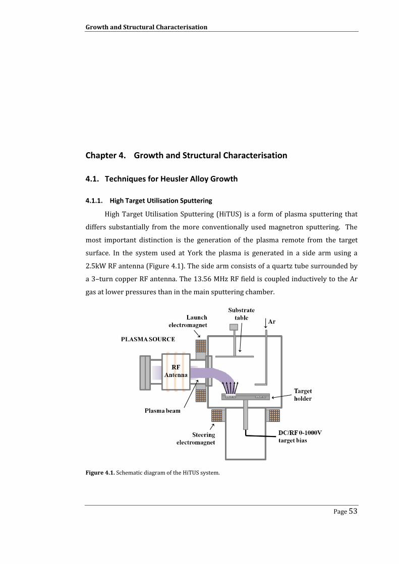
Growth and Structural Characterisation
Page 53
Chapter 4. Growth and Structural Characterisation
4.1. Techniques for Heusler Alloy Growth
4.1.1. High Target Utilisation Sputtering
High Target Utilisation Sputtering (HiTUS) is a form of plasma sputtering that
differs substantially from the more conventionally used magnetron sputtering. The
most important distinction is the generation of the plasma remote from the target
surface. In the system used at York the plasma is generated in a side arm using a
2.5kW RF antenna (Figure 4.1). The side arm consists of a quartz tube surrounded by
a 3–turn copper RF antenna. The 13.56 MHz RF field is coupled inductively to the Ar
gas at lower pressures than in the main sputtering chamber.
Figure 4.1. Schematic diagram of the HiTUS system.
Growth and Structural Characterisation
Page 54
The plasma is then launched into the sputtering chamber and steered onto the 5
cm diameter water cooled target by two electromagnets. The two magnets apply
different strength fields allowing the ions in the plasma to follow the flux lines of the
launch electromagnet into the chamber where the higher field steering electromagnet
overcomes the field from the launch electromagnet, steering the ions towards the
target surface. The ions of the Ar plasma follow field lines through a process of
ambipolar diffusion. The resulting plasma beam has a high ion density (1012 -1013
ions/cm3) [121] which allows sputtering at a high rate (0.8 Å/s). The plasma beam at
the target surface is composed of low energy ions (<10 eV) which are not of sufficient
energy to sputter material. The plasma beam is therefore coupled to a DC bias voltage
applied to the target which allows an increase of ion energy to a value above the
threshold required for sputtering. The bias voltage can be varied above this threshold
resulting in highly controlled sputtering of the target material. The separation of
plasma generation from the sputtering chamber is the key element in achieving
deposition with a wide range of controlled process parameters. It is also possible to
turn off the second electromagnet, resulting in a plasma of low energy ions (<30 eV)
surrounding the substrate holder. These low energy ions can be used to remove
surface contaminants from the substrates before film deposition [122].
Controllable parameters include the Ar ion energy at the target surface through
the applied bias to the target, the Ar ion density through control of the Ar gas flow rate
during deposition and the initial ion energy through variation of the RF power
supplied through the antenna. Variation of each of these parameters results in varying
degrees of control over the grain size distribution within the sputtered films [122].
Bias voltage, process pressure and RF power all give a monotonic increase in mean
grain diameter. As a result of this wide ranging variation in grain size with process
parameters, it is important to control a number of these parameters so that the
deposited films are comparable. The deposition of thin films in this work was carried
out at a constant process pressure (2.5×10⁻³ mbar) and RF power (1.5 kW). The grain
size or structure of the as-deposited films was therefore controlled through variation
of the DC bias voltage applied to the target. The process pressure is controlled by a
dedicated mass flow controller with the possibility to use set points for gas flow or
chamber pressure. A chamber pressure set point of 2.5×10⁻³ mbar was used which
results in an average Ar flow rate of 29.5 sccm. The RF power is controlled as a

Growth and Structural Characterisation
Page 55
percentage of the maximum power of the supply (2.5 kW) allowing 100 discreet
settings.
The HiTUS system at York also has a number of other features that make it
applicable for the deposition of a wide range of thin film structures. The sputter
targets are held in an 8 target carousel. This means that complex multi-layered
structures can be created from up to 8 eight different elements or alloys without
breaking vacuum. Due to the HiTUS eroding material from the entire target surface, it
is particularly suitable for the sputtering of alloyed targets. This feature also allows
the use of composite targets where the surface composition of the target can be varied
to change the sputtered film structure. The substrates onto which the films are
deposited are also held within a 6 substrate carousel allowing 6 samples of variable
composition to be created without breaking vacuum. Each substrate holder can hold a
maximum of one 20 × 20 mm substrate. Another important feature of the HiTUS is
that the substrate carousel is held 30 cm above the target and therefore out of the
plasma beam. The result of this is no re-sputtering from the substrate or target during
deposition, removing any unusual substrate dependent growth parameters. This
target-to-substrate distance also results in a relatively slow growth rate so that the
deposited films show excellent uniformity across the entire sample with low surface
roughness (<2 nm peak to peak).
4.1.2. Heusler Alloy Growth
The HiTUS system has recently been used for the deposition of Heusler alloy
films [123]. The group at York are the only group to use this technique for Heusler
alloy growth. Heusler alloy films deposited through HiTUS sputtering are quite unlike
any of those deposited by magnetron sputtering or MBE growth. Unlike commonly
used epitaxial films, these HiTUS grown films exhibit little or no structural ordering in
the “as-deposited state”. Through annealing, large crystals or grains begin to form out
of the as-deposited amorphous matrix. After heating for up to 6 hours, films show a
remarkable distribution in grain size with median grain diameters ranging from 30
nm to 250 nm depending upon the deposition bias voltage [124]. These films also
show a large variation in crystallographic orientation, with grains observed with
[100], [111], and [112] projections out of the plane of the film. Fleet et al. suggest that
this is a result of initial nano-crystal nucleation sites in the as-deposited matrix, with a
layer-by-layer crystallisation mechanism for those films found with [112] orientation.

Growth and Structural Characterisation
Page 56
For films annealed for longer than 6 hours, a decrease is seen in the median grain
diameters for all films. This is explained by a process of Si-segregation out of the bulk
of the ordered grains [123].
4.1.3. Magnetron Sputtering
Magnetron sputtering is one of the most widely used techniques for the
deposition of magnetic thin films, having found widespread application in the
magnetic storage industry. In the magnetron process, a glow discharge plasma is
achieved above the target and the energetic ions are accelerated towards the target
surface by a cathode situated below, to which a negative potential of a few hundred
volts is applied [125]. The bombardment of the target by ions erodes material from
the target. The rate at which material is eroded depends upon the energy and mass of
the ions, as well as the number of ions incident on the target. This ion bombardment
also leads to the emission of secondary electrons which cause further ionisation
events, helping to maintain the plasma. By applying a magnetic field parallel to the
target surface as shown in Figure 4.2, the secondary electrons can be confined near
the target surface. This increases the number of ionisation events in this region
leading to a higher density plasma and increased sputtering rates. Below the confined
electrons there is a region of increased erosion leading to a characteristic ‘race-track’
appearing on the target surface. This limits target lifetime and prevents the use of
composite targets.
Figure 4.2. Schematic diagram of a conventional magnetron sputtering system.
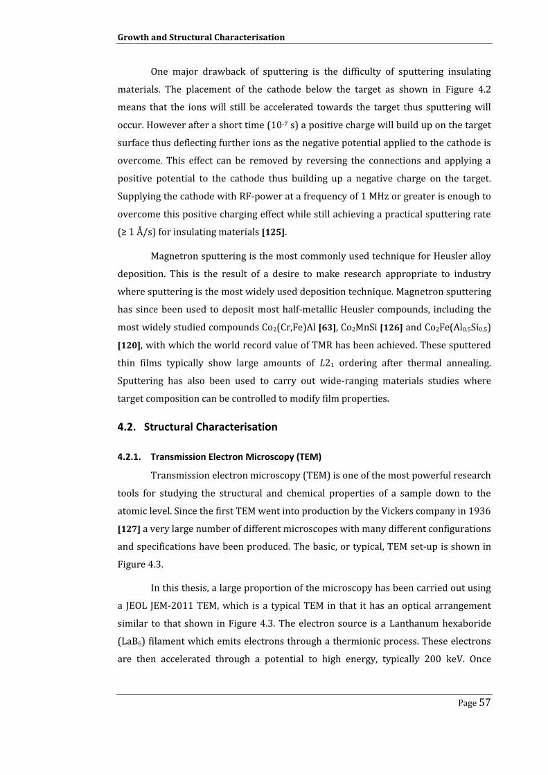
Growth and Structural Characterisation
Page 57
One major drawback of sputtering is the difficulty of sputtering insulating
materials. The placement of the cathode below the target as shown in Figure 4.2
means that the ions will still be accelerated towards the target thus sputtering will
occur. However after a short time (10-7 s) a positive charge will build up on the target
surface thus deflecting further ions as the negative potential applied to the cathode is
overcome. This effect can be removed by reversing the connections and applying a
positive potential to the cathode thus building up a negative charge on the target.
Supplying the cathode with RF-power at a frequency of 1 MHz or greater is enough to
overcome this positive charging effect while still achieving a practical sputtering rate
(≥ 1 Å/s) for insulating materials [125].
Magnetron sputtering is the most commonly used technique for Heusler alloy
deposition. This is the result of a desire to make research appropriate to industry
where sputtering is the most widely used deposition technique. Magnetron sputtering
has since been used to deposit most half-metallic Heusler compounds, including the
most widely studied compounds Co2(Cr,Fe)Al [63], Co2MnSi [126] and Co2Fe(Al0.5Si0.5)
[120], with which the world record value of TMR has been achieved. These sputtered
thin films typically show large amounts of L21 ordering after thermal annealing.
Sputtering has also been used to carry out wide-ranging materials studies where
target composition can be controlled to modify film properties.
4.2. Structural Characterisation
4.2.1. Transmission Electron Microscopy (TEM)
Transmission electron microscopy (TEM) is one of the most powerful research
tools for studying the structural and chemical properties of a sample down to the
atomic level. Since the first TEM went into production by the Vickers company in 1936
[127] a very large number of different microscopes with many different configurations
and specifications have been produced. The basic, or typical, TEM set-up is shown in
Figure 4.3.
In this thesis, a large proportion of the microscopy has been carried out using
a JEOL JEM-2011 TEM, which is a typical TEM in that it has an optical arrangement
similar to that shown in Figure 4.3. The electron source is a Lanthanum hexaboride
(LaB6) filament which emits electrons through a thermionic process. These electrons
are then accelerated through a potential to high energy, typically 200 keV. Once

Growth and Structural Characterisation
Page 58
accelerated into the microscope column the electrons are focused into a small (2-3
μm) coherent electron beam by the condenser lens. Consisting of a number of
electromagnetic lenses and apertures, this system controls the intensity and spot size
of the beam incident on the specimen. The size of the beam can then be further
restricted by a user selectable condenser aperture. This condenser aperture removes
higher angle electrons from the beam increasing the uniformity of radiation
illuminating the specimen. These apertures can also be used to limit the beam
intensity for imaging of specimens that are highly susceptible to beam damage. The
electrons then reach and interact with the specimen. This interaction happens
through a large variety of mechanisms shown schematically in Figure 4.4. Due to the
large number of interactions a number of different imaging modes can be used.
Figure 4.3. Ray diagrams for typical TEM configurations showing mechanism for the formation of images
(left) and diffraction patterns (right) [127].
The sample itself sits within the pole pieces of the objective lens. This lens
focuses the scattered transmitted electrons to form an intermediate image between
the objective and intermediate lenses. In the back focal plane of the objective lens is a

Growth and Structural Characterisation
Page 59
set of objective apertures. These allow selection of electrons scattered to specific
positions in the diffraction pattern so that different imaging modes or improved
contrast can be used. The intermediate image formed from the objective lens is
further focused and magnified by the intermediate lens. This intermediate lens is of
variable strength, which allows for the projection of either an image or a diffraction
pattern as shown in Figure 4.3. The image is then further magnified by a number of
projector lenses, not shown in the diagram, which eventually focus the image onto
either a fluorescent screen or a charge-couple device (CCD) camera.
Figure 4.4. Signals generated through electron interactions with a thin specimen in a TEM [127].
The large number of interactions between the electron beam and the specimen
allow for the use of many different imaging techniques. The most commonly used
imaging mode is bright-field imaging. In this mode, an objective aperture is inserted
into the back focal plane of the objective lens blocking electrons scattered to higher
angles, allowing only the main electron beam to pass.
Another commonly used technique is dark-field imaging. In this mode, the
objective aperture is positioned to allow only the passage of electrons scattered to a
specific position while blocking out the main beam. This technique is used for the
grain size analysis in this work as it allows imaging of grains diffracting to a specific
part of the diffraction pattern. This reduces the error associated with measuring
separate grains of similar bright field contrast as a single grain. Both these techniques
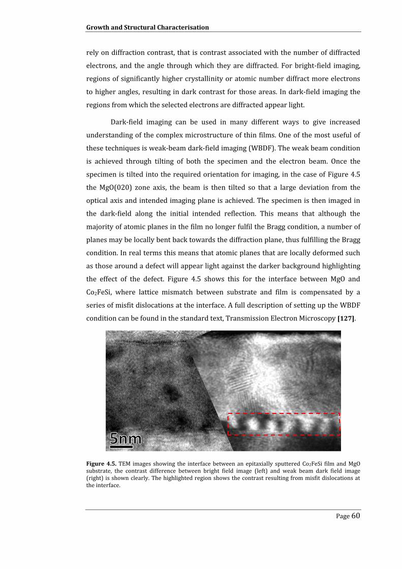
Growth and Structural Characterisation
Page 60
rely on diffraction contrast, that is contrast associated with the number of diffracted
electrons, and the angle through which they are diffracted. For bright-field imaging,
regions of significantly higher crystallinity or atomic number diffract more electrons
to higher angles, resulting in dark contrast for those areas. In dark-field imaging the
regions from which the selected electrons are diffracted appear light.
Dark-field imaging can be used in many different ways to give increased
understanding of the complex microstructure of thin films. One of the most useful of
these techniques is weak-beam dark-field imaging (WBDF). The weak beam condition
is achieved through tilting of both the specimen and the electron beam. Once the
specimen is tilted into the required orientation for imaging, in the case of Figure 4.5
the MgO(020) zone axis, the beam is then tilted so that a large deviation from the
optical axis and intended imaging plane is achieved. The specimen is then imaged in
the dark-field along the initial intended reflection. This means that although the
majority of atomic planes in the film no longer fulfil the Bragg condition, a number of
planes may be locally bent back towards the diffraction plane, thus fulfilling the Bragg
condition. In real terms this means that atomic planes that are locally deformed such
as those around a defect will appear light against the darker background highlighting
the effect of the defect. Figure 4.5 shows this for the interface between MgO and
Co2FeSi, where lattice mismatch between substrate and film is compensated by a
series of misfit dislocations at the interface. A full description of setting up the WBDF
condition can be found in the standard text, Transmission Electron Microscopy [127].
Figure 4.5. TEM images showing the interface between an epitaxially sputtered Co2FeSi film and MgO substrate, the contrast difference between bright field image (left) and weak beam dark field image (right) is shown clearly. The highlighted region shows the contrast resulting from misfit dislocations at the interface.

Growth and Structural Characterisation
Page 61
4.2.2. Selected Area Electron Diffraction (SAED)
Electron diffraction allows some of the most detailed structural analysis that
can be performed in a TEM. If a crystal structure is present in the specimen then
electrons passing through will be diffracted by the atomic potentials to particular
conditions that satisfy the Laue condition for constructive interference, equation 4.1.
(4.1)
where L is the vector describing the difference between the incident and exit electron
beam due to diffraction, and g is the vector describing the reciprocal space positions
of an atomic plane. However these are often simplified to the Bragg condition
equation 4.2 for specific atomic positions.
(4.2)
where λe is the de Broglie wavelength of the electron, θB is the angle between the
incident electron beam and the diffracting lattice planes which satisfies the Bragg
condition and dhkl is the spacing of lattice planes given by equation 4.3
√
(4.3)
For cubic crystals a is the lattice parameter and h, k, and l are the Miller indices
corresponding to the particular diffracting plane [127]. Electron reflections that
satisfy these conditions result in bright spots or rings dependent upon the specimen.
The diffraction pattern can then be analysed to give information about the
crystallinity of a sample (whether it is mono or polycrystalline) and if there are
multiple phases of material in the specimen. This last point is particularly useful for
Heusler alloys where a number of different disordered phases may exist in a single
specimen. Diffraction can also give extremely important information about the
epitaxial relationship between different layers in a film.
These parameters are true for any TEM beam size. However, for various
reasons it is often unsuitable to take a diffraction pattern from a large area, most
notably that the specimen may often be buckled giving a confused pattern. This can be
overcome by a number of techniques, including converging the beam to a small spot
(CBED) but most easily and usually through the use of selected area electron
diffraction (SAED). In this technique an aperture is inserted exactly into the image

Growth and Structural Characterisation
Page 62
plane of one of the lenses subsequent to the specimen, thus creating a virtual aperture
at the specimen plane. It is important to focus the diffracting beam correctly so that
the aperture is exactly conjugate with the specimen. Then any electron hitting the
specimen outside the defined aperture also hits the real aperture as well [127].
Figure 4.6. a) SAED diffraction pattern from a Fe3Si interface showing monocrystalline diffraction pattern. b) SAED diffraction pattern of polycrystalline Co2FeSi film.
Figure 4.6 shows typical SAED patterns for monocrystalline and
polycrystalline thin films. The monocrystalline pattern shows spots in specific
positions depending on the reflections that obey the Bragg conditions. This can be
used to easily evaluate the epitaxial relationship between film and substrate. The
intensity of spots in these diffraction patterns can in principle give quantitative
information about ordering in the film. However, this is difficult to achieve as
thickness variation and sample tilt can result in increased or reduced intensities
across the diffraction pattern. The appearance of particular allowed reflections due to
different material phases is however easily observed, which makes SAED diffraction of
this type useful for identifying B2 and L21 ordered Heusler alloy films. The random
orientation of grains in the polycrystalline specimen results in a rotation of the
reciprocal lattice through all axes producing a ring pattern as seen in Figure 4.6b. This
is analogous to X-ray diffraction as described in section 4.2.5. The radial separation of
the rings from the main beam is the result of specific reflections. However, due to the
complex structure of the polycrystalline films in this study, these rings are widened or
smoothed resulting in hard to analyse patterns. Some of the rings are made of
discrete spots due to the large grains in the specimen [127].

Growth and Structural Characterisation
Page 63
4.2.3. High Resolution TEM with Aberration Correction
A large amount of work in this thesis is focused towards the characterisation
of the crystallographic structure of the various samples. In order to image this
crystallographic (or even atomic) structure, resolution in the sub angstrom regime
must be achieved. In situations like this, a typical microscope such as the JEOL JEM-
2011 used in some of this work may not be enough. The accessible resolution in a
TEM image is the result of the Fourier transform of the accessible spatial frequencies
resulting from the diffracted electron beam after transmission through the sample.
For high resolution imaging, high spatial frequencies must be accessed. There are two
main contributing factors to the resolution limit in TEM. One term from the
microscope and one term from the specimen itself. The term from the specimen can
be summed up as a specimen thickness term. If the specimen is thin enough that the
amplitude of the project potential of the specimen is linearly related to the amplitude
of the transmitted wave, this is known as the weak phase approximation.
The term from the microscope is described by what is often called the contrast
transfer function of the microscope T(u), where u is the spatial frequency [127].
( ) ( ) ( ) ( ) (4.4)
Here A(u) is the aperture term, which is simply adjustable dependent on the radius of
aperture used while imaging. The two more complex terms are the envelope term
E(u) and the aberration term B(u). First let us address the envelope term, which forms
a damping term and a cut-off point for the accessible spatial frequencies. The largest
contribution to this envelope term comes from the spatial coherence of the
illumination, or what is also known as chromatic aberration. To reduce this aberration
the energy spread of the electrons from the gun must be controlled. The JEOL JEM-
2011 typically uses a LaB6 filament and thermionic emission to form the electron
beam. The typical energy spread from such a source is ~1.5 eV (at FWHM). The JEOL
JEM-2200FS also used in this work uses a field emission gun with a typical energy
spread of 0.3 eV or 5 times smaller than that of hot emission guns [127]. The change of
gun instantly improves the range of accessible spatial frequencies.
The final term in equation 4.4 is the aberration term, which is most commonly
expressed in terms of an exponential with the exponent 𝜂(u) [127].
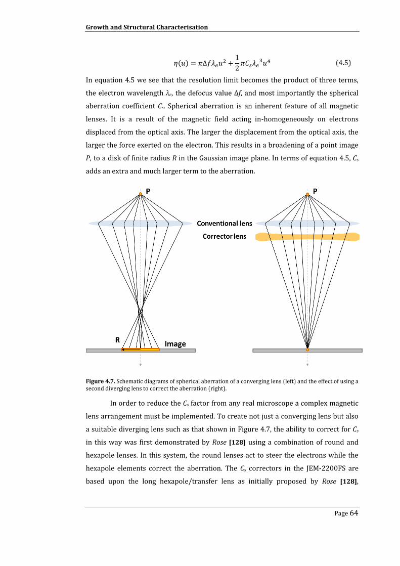
Growth and Structural Characterisation
Page 64
In equation 4.5 we see that the resolution limit becomes the product of three terms,
the electron wavelength λe, the defocus value Δf, and most importantly the spherical
aberration coefficient Cs. Spherical aberration is an inherent feature of all magnetic
lenses. It is a result of the magnetic field acting in-homogeneously on electrons
displaced from the optical axis. The larger the displacement from the optical axis, the
larger the force exerted on the electron. This results in a broadening of a point image
P, to a disk of finite radius R in the Gaussian image plane. In terms of equation 4.5, Cs
adds an extra and much larger term to the aberration.
Figure 4.7. Schematic diagrams of spherical aberration of a converging lens (left) and the effect of using a second diverging lens to correct the aberration (right).
In order to reduce the Cs factor from any real microscope a complex magnetic
lens arrangement must be implemented. To create not just a converging lens but also
a suitable diverging lens such as that shown in Figure 4.7, the ability to correct for Cs
in this way was first demonstrated by Rose [128] using a combination of round and
hexapole lenses. In this system, the round lenses act to steer the electrons while the
hexapole elements correct the aberration. The Cs correctors in the JEM-2200FS are
based upon the long hexapole/transfer lens as initially proposed by Rose [128],
𝜂( )
(4.5)

Growth and Structural Characterisation
Page 65
allowing correction of spherical aberration out to the third order. This however means
that a fifth order term of the aberration remains. The microscope must therefore be
carefully and correctly aligned to minimise this fifth order term.
The coefficients for the aberration are calculated using a tableau of
diffractograms from an amorphous sample, through an extension of the method
proposed by Zemlin et al. [129]. By analysing the digital diffractograms of images
taken at various beam tilts the spherical aberration coefficients can be derived. From
these coefficients, the currents required by the corrector lenses are calculated by
software developed by Corrected Electron Optical Systems (CEOS). This process is
repeated until the aberration coefficients are sufficiently low.
4.2.4. Scanning TEM (STEM) and its Application for Heusler Alloys.
Although initially developed in the 1930s, it was not until the late 1960s that
Scanning Transmission Electron Microscopy (STEM) became widely used due to the
development of field emission sources [129]. This is because of the increased current
densities ( A/m2) over the conventional thermionic filaments. This high current
density allows large signals to be collected from a thin specimen whilst maintaining an
extremely small probe size.
The STEM varies from the conventional TEM in a number of ways, primarily
the imaging mode. In the STEM the electron beam is focused to a small probe on the
specimen and then raster scanned to collect the information for the image as opposed
to parallel illumination of the entire imaged region. With this optical arrangement
High Angle Annular Dark Field detectors (HAADF) can be used. HAADF detectors
collect electrons scattered elastically from the specimen, the result of which is an
image contrast formed from the atomic numbers of elements in the specimen (z-
contrast). This technique is particularly useful for the structural analysis of Heusler
alloys where the z-contrast allows direct analysis of atomic elements in the lattice
[35]. A schematic of the STEM set up can be seen in Figure 4.8.
STEM can also be used in bright-field mode, where the signal is similar to
those seen in conventional TEM. Both HAADF and bright field images taken with the
JEOL JEM-2200FS can be seen in Figure 4.9a. The contrast difference is distinctive. In
HAADF mode the elements of higher z scatter more electrons to higher angles and
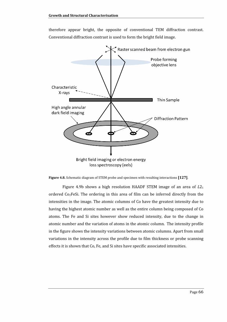
Growth and Structural Characterisation
Page 66
therefore appear bright, the opposite of conventional TEM diffraction contrast.
Conventional diffraction contrast is used to form the bright field image.
Figure 4.8. Schematic diagram of STEM probe and specimen with resulting interactions [127].
Figure 4.9b shows a high resolution HAADF STEM image of an area of L21
ordered Co2FeSi. The ordering in this area of film can be inferred directly from the
intensities in the image. The atomic columns of Co have the greatest intensity due to
having the highest atomic number as well as the entire column being composed of Co
atoms. The Fe and Si sites however show reduced intensity, due to the change in
atomic number and the variation of atoms in the atomic column. The intensity profile
in the figure shows the intensity variations between atomic columns. Apart from small
variations in the intensity across the profile due to film thickness or probe scanning
effects it is shown that Co, Fe, and Si sites have specific associated intensities.

Growth and Structural Characterisation
Page 67
Figure 4.9. a) Bright field and HAADF STEM images of an Fe3Si/Ge interface. b) Filtered high resolution HAADF STEM image of a Co2FeSi film cross section. Intensity profile along the [001] plane shows z-contrast of atoms in the alloy. Atoms are highlighted for reference, Blue (Co), Green (Fe) and Red (Si).
Another advantage of using a focused probe for electron microscopy is high
resolution elemental mapping through energy dispersive x-ray (EDX) spectroscopy.
Using the rastered electron beam, elemental maps of entire regions or line scans
through multilayer films can be acquired. The information from these is difficult to
quantify. This difficulty arises for a number of reasons. One of the most prevalent is
specimen drift during the measurement. The extremely long exposure times involved
in these measurements also results in increased specimen damage and contamination.
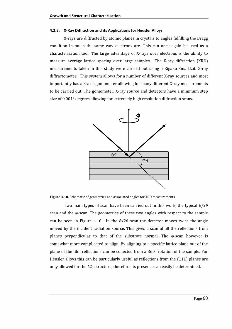
Growth and Structural Characterisation
Page 68
4.2.5. X-Ray Diffraction and its Applications for Heusler Alloys
X-rays are diffracted by atomic planes in crystals to angles fulfilling the Bragg
condition in much the same way electrons are. This can once again be used as a
characterisation tool. The large advantage of X-rays over electrons is the ability to
measure average lattice spacing over large samples. The X-ray diffraction (XRD)
measurements taken in this study were carried out using a Rigaku SmartLab X-ray
diffractometer. This system allows for a number of different X-ray sources and most
importantly has a 3-axis goniometer allowing for many different X-ray measurements
to be carried out. The goniometer, X-ray source and detectors have a minimum step
size of 0.001° degrees allowing for extremely high resolution diffraction scans.
Figure 4.10. Schematic of geometries and associated angles for XRD measurements.
Two main types of scan have been carried out in this work, the typical θ/2θ
scan and the φ-scan. The geometries of these two angles with respect to the sample
can be seen in Figure 4.10. In the θ/2θ scan the detector moves twice the angle
moved by the incident radiation source. This gives a scan of all the reflections from
planes perpendicular to that of the substrate normal. The φ-scan however is
somewhat more complicated to align. By aligning to a specific lattice plane out of the
plane of the film reflections can be collected from a 360° rotation of the sample. For
Heusler alloys this can be particularly useful as reflections from the (111) planes are
only allowed for the L21 structure, therefore its presence can easily be determined.

Growth and Structural Characterisation
Page 69
The full width half maximum (FWHM) of a peak can be used to estimate the
crystallite size within a film using the Scherrer relationship, equation 4.6.
where DXRD is the crystallite size , λx is the wavelength of the incident X-ray radiation, β
is the FWHM and θB is the Bragg angle of the peak [130]. This is used in this work to
estimate the size of L21 ordered regions in films. It should be noted however that for
large particles this equation will provide an underestimate. This is due to the effect of
lattice strain on the diffraction patterns for these particles.
(4.6)
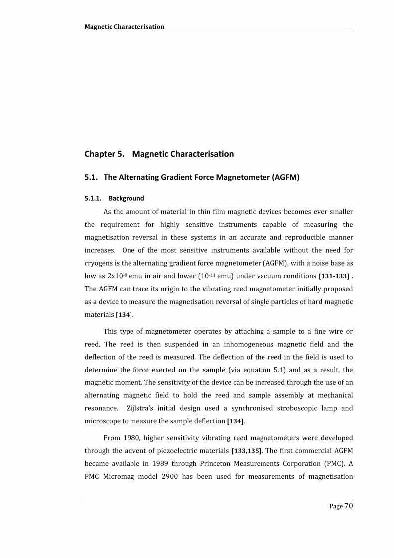
Magnetic Characterisation
Page 70
Chapter 5. Magnetic Characterisation
5.1. The Alternating Gradient Force Magnetometer (AGFM)
5.1.1. Background
As the amount of material in thin film magnetic devices becomes ever smaller
the requirement for highly sensitive instruments capable of measuring the
magnetisation reversal in these systems in an accurate and reproducible manner
increases. One of the most sensitive instruments available without the need for
cryogens is the alternating gradient force magnetometer (AGFM), with a noise base as
low as 2x10⁻⁸ emu in air and lower (10-11 emu) under vacuum conditions [131-133] .
The AGFM can trace its origin to the vibrating reed magnetometer initially proposed
as a device to measure the magnetisation reversal of single particles of hard magnetic
materials [134].
This type of magnetometer operates by attaching a sample to a fine wire or
reed. The reed is then suspended in an inhomogeneous magnetic field and the
deflection of the reed is measured. The deflection of the reed in the field is used to
determine the force exerted on the sample (via equation 5.1) and as a result, the
magnetic moment. The sensitivity of the device can be increased through the use of an
alternating magnetic field to hold the reed and sample assembly at mechanical
resonance. Zijlstra’s initial design used a synchronised stroboscopic lamp and
microscope to measure the sample deflection [134].
From 1980, higher sensitivity vibrating reed magnetometers were developed
through the advent of piezoelectric materials [133,135]. The first commercial AGFM
became available in 1989 through Princeton Measurements Corporation (PMC). A
PMC Micromag model 2900 has been used for measurements of magnetisation
Magnetic Characterisation
Page 71
reversal of continuous thin film samples in this work. The AGFM is a force based
instrument. The AGFM arrangement of the PMC system is shown schematically in
Figure 5.1.
Figure 5.1. Schematic diagram of a typical AGFM.
The alternating gradient field produced by the small coils attached to the pole
pieces induces small deflections (~nm) in the sample and as a result a stress upon the
sample mounting assembly. This assembly is in turn attached to a silver-coated lead-
zirconate-titanate (PZT) piezoelectric bimorph. This bimorph converts the stress
exerted on it by the sample deflection into a measurable voltage. The force exerted on
the sample by the gradient field is given by:
( )
(5.1)
where i is an arbitrary direction along which all components of the equations are
measured (i= x, y, z) and μi and (dH/di) are the magnetic moment and field gradient
measured along i respectively. As previously discussed, the sensitivity of the AGFM
can be maximised by operating at the mechanical resonance of the sample mounting
assembly. This mounting assembly consists of two tubular quartz legs, roughly 25 mm

Magnetic Characterisation
Page 72
long with 0.4 mm outer diameter, attached to a quartz glass plate of similar size to the
sample. Equation 5.2 gives the resonant frequency (νres)
(
)
⁄
(5.2)
Where the variables refer to the dimensions and properties of the quartz legs and
mounting plate, the width w, the length l and density ρ and Young’s modulus Y.
Operating at νres should give a high mechanical Q-factor (25-250) [131], although the
Q-factors of probes used in this work varied between 25 and 74. A measurement of
the noise base of a typical probe is shown in Figure 5.2. The standard deviation in
1000 measurements of a moment of 3.56x10⁻⁴ emu over 100 seconds is 1x10⁻⁶ emu
whilst using a field gradient of 0.4 Oe/mm. The noise base is somewhat higher than
that previously quoted from the reference[132]. This is due to the use of a much
smaller field gradient, 0.4 Oe/mm instead of 4 Oe/mm, resulting in smaller deflections
of the probe. The resonant frequency of the combined assembly and sample is
determined before taking measurements by sweeping the gradient field through a
frequency range, typically 100-1000 Hz, and measuring the output voltage, which
peaks at vres.
Once νres has been determined the magnetic properties of the sample can be
measured. A wide range of magnetic measurements can be performed with this
instrument, most commonly hysteresis loops, DC demagnetised (DCD) and isothermal
remanence curves (IRM) as well as measurements of magnetic time dependence. The
PMC Micromag model 2900 AGFM is equipped with a water-cooled low impedance
electromagnet, producing a maximum field of 24 kOe at a pole spacing of 10 mm with
a high sweep rate. The typical measurement time for a simple symmetric hysteresis
loop between ±5 kOe is 90 seconds. It is also possible to adapt the system for use with
a continuous-flow cryostat allowing measurement at temperatures between 4 and
300K although this is known to raise the noise base of the system to 2×10⁻⁵ emu with a
field gradient of 4 Oe/mm at 5 K [132].
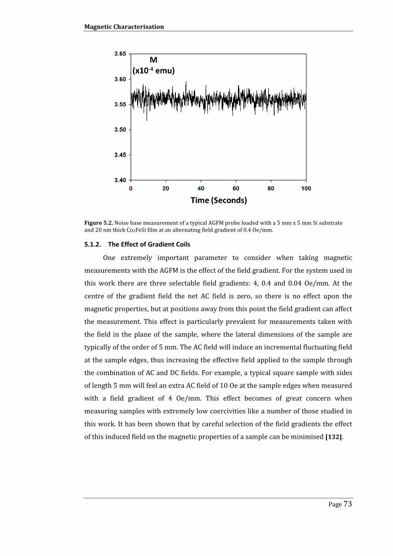
Magnetic Characterisation
Page 73
Figure 5.2. Noise base measurement of a typical AGFM probe loaded with a 5 mm x 5 mm Si substrate and 20 nm thick Co2FeSi film at an alternating field gradient of 0.4 Oe/mm.
5.1.2. The Effect of Gradient Coils
One extremely important parameter to consider when taking magnetic
measurements with the AGFM is the effect of the field gradient. For the system used in
this work there are three selectable field gradients: 4, 0.4 and 0.04 Oe/mm. At the
centre of the gradient field the net AC field is zero, so there is no effect upon the
magnetic properties, but at positions away from this point the field gradient can affect
the measurement. This effect is particularly prevalent for measurements taken with
the field in the plane of the sample, where the lateral dimensions of the sample are
typically of the order of 5 mm. The AC field will induce an incremental fluctuating field
at the sample edges, thus increasing the effective field applied to the sample through
the combination of AC and DC fields. For example, a typical square sample with sides
of length 5 mm will feel an extra AC field of 10 Oe at the sample edges when measured
with a field gradient of 4 Oe/mm. This effect becomes of great concern when
measuring samples with extremely low coercivities like a number of those studied in
this work. It has been shown that by careful selection of the field gradients the effect
of this induced field on the magnetic properties of a sample can be minimised [132].
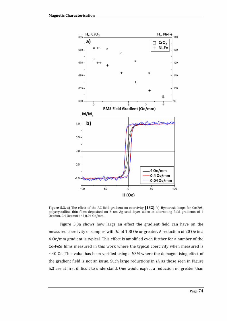
Magnetic Characterisation
Page 74
Figure 5.3. a) The effect of the AC field gradient on coercivity [132]. b) Hysteresis loops for Co2FeSi polycrystalline thin films deposited on 6 nm Ag seed layer taken at alternating field gradients of 4 Oe/mm, 0.4 Oe/mm and 0.04 Oe/mm.
Figure 5.3a shows how large an effect the gradient field can have on the
measured coercivity of samples with Hc of 100 Oe or greater. A reduction of 20 Oe in a
4 Oe/mm gradient is typical. This effect is amplified even further for a number of the
Co2FeSi films measured in this work where the typical coercivity when measured is
~40 Oe. This value has been verified using a VSM where the demagnetising effect of
the gradient field is not an issue. Such large reductions in Hc as those seen in Figure
5.3 are at first difficult to understand. One would expect a reduction no greater than
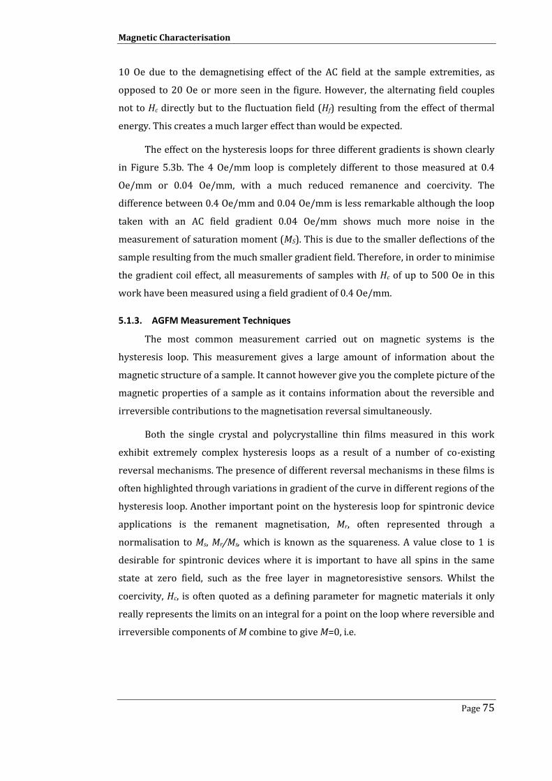
Magnetic Characterisation
Page 75
10 Oe due to the demagnetising effect of the AC field at the sample extremities, as
opposed to 20 Oe or more seen in the figure. However, the alternating field couples
not to Hc directly but to the fluctuation field (Hf) resulting from the effect of thermal
energy. This creates a much larger effect than would be expected.
The effect on the hysteresis loops for three different gradients is shown clearly
in Figure 5.3b. The 4 Oe/mm loop is completely different to those measured at 0.4
Oe/mm or 0.04 Oe/mm, with a much reduced remanence and coercivity. The
difference between 0.4 Oe/mm and 0.04 Oe/mm is less remarkable although the loop
taken with an AC field gradient 0.04 Oe/mm shows much more noise in the
measurement of saturation moment (MS). This is due to the smaller deflections of the
sample resulting from the much smaller gradient field. Therefore, in order to minimise
the gradient coil effect, all measurements of samples with Hc of up to 500 Oe in this
work have been measured using a field gradient of 0.4 Oe/mm.
5.1.3. AGFM Measurement Techniques
The most common measurement carried out on magnetic systems is the
hysteresis loop. This measurement gives a large amount of information about the
magnetic structure of a sample. It cannot however give you the complete picture of the
magnetic properties of a sample as it contains information about the reversible and
irreversible contributions to the magnetisation reversal simultaneously.
Both the single crystal and polycrystalline thin films measured in this work
exhibit extremely complex hysteresis loops as a result of a number of co-existing
reversal mechanisms. The presence of different reversal mechanisms in these films is
often highlighted through variations in gradient of the curve in different regions of the
hysteresis loop. Another important point on the hysteresis loop for spintronic device
applications is the remanent magnetisation, Mr, often represented through a
normalisation to Ms, Mr/Ms, which is known as the squareness. A value close to 1 is
desirable for spintronic devices where it is important to have all spins in the same
state at zero field, such as the free layer in magnetoresistive sensors. Whilst the
coercivity, Hc, is often quoted as a defining parameter for magnetic materials it only
really represents the limits on an integral for a point on the loop where reversible and
irreversible components of M combine to give M=0, i.e.

Magnetic Characterisation
Page 76
∫ ( ) ( ) ∫ ( ) ∫ ( )
(5.2)
where g(H) is the Langevin function describing the reversible component, f(ΔE) is the
distribution of energy barriers in the system and ΔEc is the critical energy barrier that
is undergoing thermal activation at the measurement time.
Figure 5.4. Coercivity of a magnetic system described through a distribution of energy barriers.
This expansion of integrals in equation 5.2 describes the coercive mechanism
through a distribution of energy barriers shown schematically in Figure 5.4. The
coercivity is the point where the volume of reversible and irreversible energy barriers
in one magnetisation direction balances the irreversible component in the opposite
direction resulting in a net magnetisation of zero. The reversible component can be
due to thermal energy or misalignment of the easy axes which gives the dependence
of Hc on measurement parameters. As a result, it is often more important to measure
the irreversible components of the magnetisation, which can be achieved through
measurements of remanence curves.
Measurements of Mr provide an important understanding of a number of
properties of magnetic thin films, through which it is possible to determine both the
reversible and irreversible components of the magnetisation. These measurements
are one route to determine Hf and as a result the magnetic activation volume (section
2.5). Remanence can be measured either by taking the system from an initially
demagnetised state to positive saturation in an isothermal remanence (IRM) curve, or
from positive saturation to negative saturation known as a DC demagnetisation (DCD)
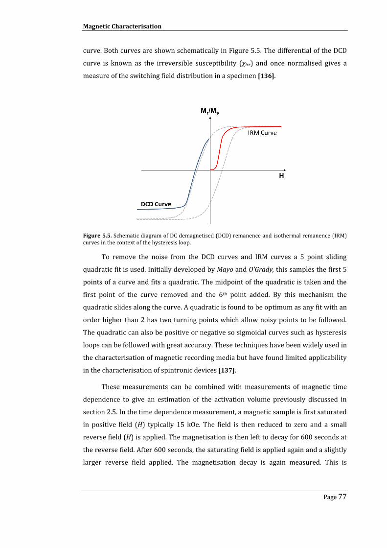
Magnetic Characterisation
Page 77
curve. Both curves are shown schematically in Figure 5.5. The differential of the DCD
curve is known as the irreversible susceptibility (χirr) and once normalised gives a
measure of the switching field distribution in a specimen [136].
Figure 5.5. Schematic diagram of DC demagnetised (DCD) remanence and isothermal remanence (IRM) curves in the context of the hysteresis loop.
To remove the noise from the DCD curves and IRM curves a 5 point sliding
quadratic fit is used. Initially developed by Mayo and O’Grady, this samples the first 5
points of a curve and fits a quadratic. The midpoint of the quadratic is taken and the
first point of the curve removed and the 6th point added. By this mechanism the
quadratic slides along the curve. A quadratic is found to be optimum as any fit with an
order higher than 2 has two turning points which allow noisy points to be followed.
The quadratic can also be positive or negative so sigmoidal curves such as hysteresis
loops can be followed with great accuracy. These techniques have been widely used in
the characterisation of magnetic recording media but have found limited applicability
in the characterisation of spintronic devices [137].
These measurements can be combined with measurements of magnetic time
dependence to give an estimation of the activation volume previously discussed in
section 2.5. In the time dependence measurement, a magnetic sample is first saturated
in positive field (H) typically 15 kOe. The field is then reduced to zero and a small
reverse field (H) is applied. The magnetisation is then left to decay for 600 seconds at
the reverse field. After 600 seconds, the saturating field is applied again and a slightly
larger reverse field applied. The magnetisation decay is again measured. This is
Magnetic Characterisation
Page 78
repeated through the entire reversal curve of the hysteresis loop from remanence to
negative saturation. The result of this is a series of decay curves at different values of
reverse field such as those shown in Figure 5.6. It is shown that in this case M ∝ ln(t).
Figure 5.6. Time dependence curves taken every 5 Oe showing variation of M with ln(time) for polycrystalline Co2FeSi film deposited at 800 V and annealed at 500°C for 6 hours.
( ) ( ) ( ) ( )
(5.3)
Plotting the decay curves versus ln(t) allows access to the magnetic viscosity
coefficients, S(H), needed for the estimation of the activation volume. In some
magnetic systems however the simple linear case may not be applied. S(H) is
intrinsically linked to the energy barrier distribution. For systems with a very narrow
energy barrier distribution variation of M with ln(t) becomes non-linear. In these
situations the decay of M is more accurately described by the series expansion of
equation 5.3 [138].
( ) ( ) ( ) ( ) ( )[ ( )]
(5.4)
From the values of S(H) and the irreversible susceptibility it is possible to find
an estimation for Hf which is essential for any calculations of the activation volume
(Vact). It is also possible to acquire a value of Hf directly from the magnetisation decay
curves using the waiting time method [75]. With a series of magnetisation decay

Magnetic Characterisation
Page 79
curves closely spaced in H it is possible to select a point of constant magnetisation
which has a number of intercepts from which Hf can be determined [77].
Figure 5.7. The effect of pole piece separation on the AC-gradient field in the PMC micromag 2100 AGFM.
Unfortunately, for samples with extremely low coercivities like the epitaxial
films measured in this work, it is impossible to acquire decay curves with sufficient
resolution to perform a waiting time measurement (or even a high resolution
calculation of Hf using the S(H) and χirr method). This is due to the limit of
controllability of the DC field from the AGFM. It is possible to improve this resolution
by separating the pole pieces of the magnet so that each incremental current step
produces a smaller step in field. However, this also results in a reduction of the
gradient field from the calibrated 4 Oe/mm at 11 mm spacing.
The effect of pole spacing on AC field magnitude was then measured. A 620 turn
coil was fixed between the pole pieces and connected to a digital oscilloscope through
a lock-in amplifier. A sine wave from a signal generator was used as the reference with
a frequency set to the operating frequency of the AGFM probes used for
measurements. The peak-peak (p-p) voltage induced in the coil could then be
measured to high accuracy. By using the initial PMC calibration this p-p voltage could
be converted to a field gradient value in Oe/mm. The effect of pole spacing on the
gradient field can be seen in Figure 5.7, where the field gradient drops off as the
square of the pole piece separation. To maintain reproducibility of the measurements
the spacing was set so that the relative gradient 1 setting in the AGFM software now
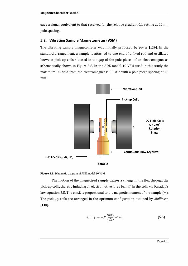
Magnetic Characterisation
Page 80
gave a signal equivalent to that received for the relative gradient 0.1 setting at 11mm
pole spacing.
5.2. Vibrating Sample Magnetometer (VSM)
The vibrating sample magnetometer was initially proposed by Foner [139]. In the
standard arrangement, a sample is attached to one end of a fixed rod and oscillated
between pick-up coils situated in the gap of the pole pieces of an electromagnet as
schematically shown in Figure 5.8. In the ADE model 10 VSM used in this study the
maximum DC field from the electromagnet is 20 kOe with a pole piece spacing of 40
mm.
Figure 5.8. Schematic diagram of ADE model 10 VSM.
The motion of the magnetised sample causes a change in the flux through the
pick-up coils, thereby inducing an electromotive force (e.m.f.) in the coils via Faraday’s
law equation 5.5. The e.m.f. is proportional to the magnetic moment of the sample (m).
The pick-up coils are arranged in the optimum configuration outlined by Mallinson
[140].
(
)
(5.5)
Magnetic Characterisation
Page 81
where N is the number of turns in the pickup coils and ⁄ is the rate of change of
the flux in the coil. The voltage induced is measured using a lock-in amplifier.
The advantage of the VSM over the AGFM is the lack of the gradient field, thus
removing the demagnetising effect and allowing for more precise measurements of
the coercivity in magnetically soft materials. The ADE model 10 also has a number of
other significant advantages over the AGFM, predominantly the ability to work at a
range of temperatures. In the ADE model 10 the pick-up coils are mounted inside a
continuous flow cryostat, which allows measurements to be made between 100K and
770K with a temperature stability of ±1K over 60 minutes. The other large advantage
is the ability to rotate the DC field coils through 270° about the sample centre,
allowing for directional dependent measurements of the magnetic moments. To aid
this ability two different sample rod designs are available, the ‘steering wheel’ where
the sample plane is fixed perpendicular to the vibration direction and the ‘lollipop’
where the sample plane is fixed parallel to the vibration direction. These allow for the
magnetic properties of the sample to be probed 270° around the plane of the sample,
and 180° out of the plane of the sample. The ability to probe the magnetic properties
around the plane of the sample is particularly useful for measurement of the easy axis
in single crystal films like the ones measured in this thesis.

The Effect of Structure on Magnetisation Reversal
Page 82
Chapter 6. The Effect of Structure on Magnetisation Reversal
The structure of magnetic thin films has long been known to have a significant effect
on magnetisation reversal [47]. The volumes of the particles within a film, as well as
any defects within those particles, all control the magnetisation reversal of the film.
Reversal is dominated by the exchange interaction between neighbouring spins, any
local structural anomalies can have a profound effect on the reversal process. This can
be in the form of domain wall pinning, reduced nucleation fields and even the point at
which particles begin to exhibit single domain behaviour. It is important to
understand how changes in the structure of Heusler alloy thin films affect the
magnetic reversal characteristics. Whether that is the change from polycrystalline to
epitaxial films, the differences between L21 and B2 ordering or the appearance of
defects in the crystal structure. A wide range of structural and magnetic
characterisation has been carried out on epitaxially sputtered and polycrystalline thin
films, sputtered using the HiTUS system, to compare the differences in magnetisation
reversal in the context of their different structures.
6.1. Film Growth and Sample Preparation
Magnetic and structural characterisation has been carried out on Co2FeSi thin
films deposited via HiTUS and UHV magnetron sputtering. 20 nm thick Co2FeSi films
were deposited and capped with a 3 nm thick Ta layer. HiTUS sputtered samples were
deposited onto both Si and MgO substrates as well as carbon coated Cu and SiN TEM
grids. The magnetron sputtered films were deposited onto MgO (001) substrates at an
average deposition rate of 0.3 Å/s. Before the Heusler layer deposition the MgO(001)
substrates were annealed for 30 minutes at 800°C to out-gas. A 10 nm MgO buffer
layer was deposited using e-beam evaporation to improve surface roughness.
Magnetron sputtered films were post-deposition annealed for 1 hour under vacuum of
The Effect of Structure on Magnetisation Reversal
Page 83
5x10⁻⁵ Pa at temperatures of 500°C and 600°C. This allows recrystallisation of the film
from the as-deposited state, which is predominantly B2 ordered, to a state with
increased L21 ordering. Samples grown using the HiTUS system were post-deposition
annealed at 500°C in an Ar atmosphere. Specimens were annealed for increasing
periods of time from 1 hour to 9 hours. This allows crystallisation of grains from the
as-deposited matrix. The films deposited onto SiN TEM grids have been annealed
inside the JEOL JEM-2200FS to observe the grain crystallisation and development
process.
6.2. Structural Characterisation
6.2.1. Polycrystalline Films
6.2.1.1. In-Situ Observation of Grain Formation
After deposition using the HiTUS system, the films were annealed in the HRTEM
to facilitate the growth of Co2FeSi grains from the nano-crystalline matrix. To
characterise the as-deposited matrix, TEM images were taken at a magnification of
x106. These images were then Fourier transformed to form the digital diffractograms
which are shown in Figure 6.1. The images show crystalline diffraction spots with
increasing intensity within the disk associated with an amorphous film. Although
these spots are present in the sample deposited with a DC bias (VB) of 500 V, their
intensity and number are shown to increase in the diffractograms of the films
deposited using a higher bias of 750 V and 990 V. This is evidence that the
crystallographic ordering in the as-deposited matrix increases with sputtering bias
voltage (VB). It also suggests that the initial crystallites in the matrix are larger when
samples are grown at higher VB. Electron dispersive X-ray spectroscopy (EDX) was
used to analyse the elemental composition of the as deposited matrix. The EDX
spectra show no significant variation in elemental composition of the matrix with VB,
thus the increased intensity of diffraction spots is purely due to the variation in film
structure and initial crystallite size induced by VB.
VB alters the initial state of the film indirectly. The voltage applied to the target
during sputtering accelerates the Ar+ ions towards the target. Higher VB therefore
leads to higher ion velocity at the target surface. This higher velocity means that the
material sputtered from the target has an increased initial energy. Because of this the
adatoms of material sputtered at higher VB will have an increased energy and

The Effect of Structure on Magnetisation Reversal
Page 84
therefore mobility upon reaching the substrate. The increased mobility results in
more of the deposited atoms forming energetically favourable ordered structures
within the film. The result of this is an increased size and number of crystallites in the
as-deposited film as shown in Figure 6.1.
Figure 6.1. Digital diffractograms from HRTEM images as well as EDX spectra for as-deposited Co2FeSi thin films with DC bias voltages of 500V, 750V and 990V.
To observe the crystallisation process induced by annealing, HRTEM with an in-
situ heating stage was used. Initial crystallisation occurs above 235°C with further
grain growth occurring after continued heating either at 235°C or higher
temperatures. Figure 6.2a shows the process of crystallisation whilst holding the
specimen at 235°C for 3 hours. It is worth noting that this experiment was carried out
with the sample continuously exposed to the electron beam during heating. However
the experiment was repeated with the beam isolation valve only opened
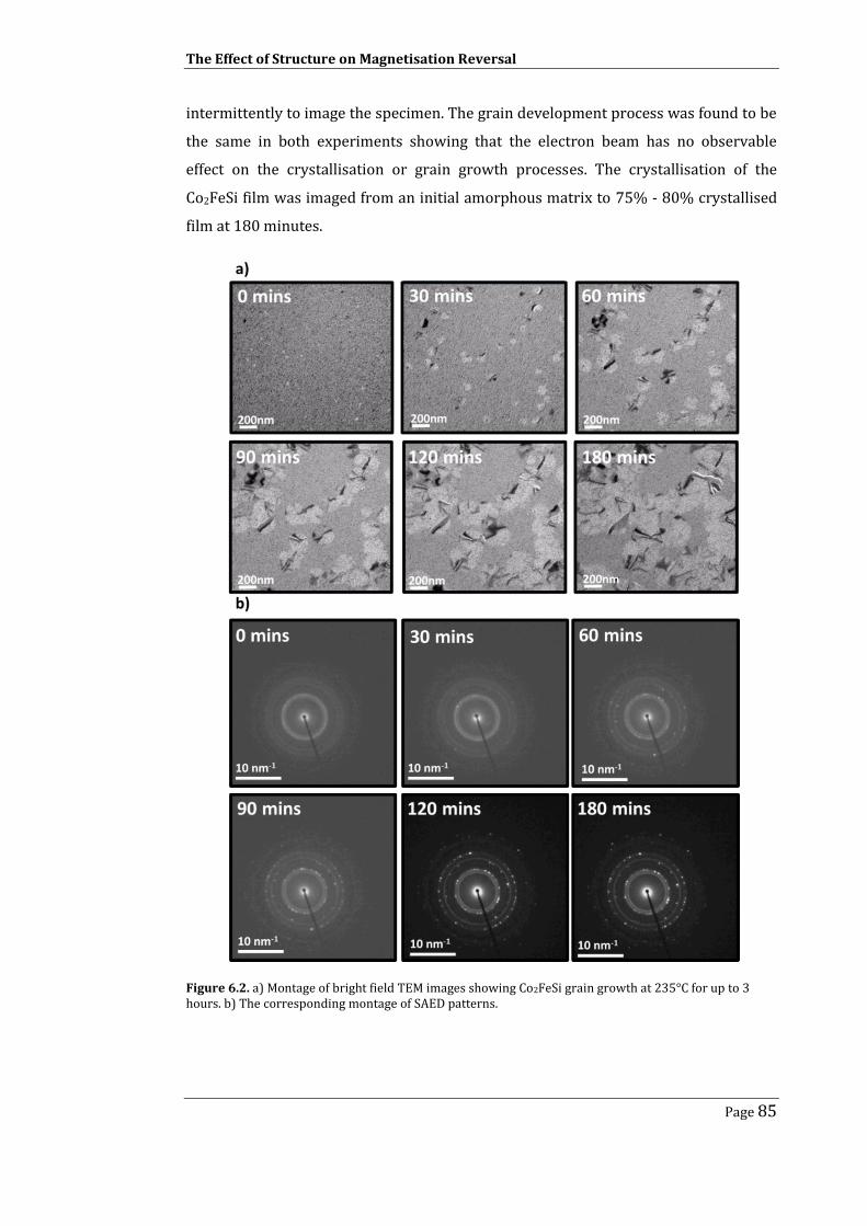
The Effect of Structure on Magnetisation Reversal
Page 85
intermittently to image the specimen. The grain development process was found to be
the same in both experiments showing that the electron beam has no observable
effect on the crystallisation or grain growth processes. The crystallisation of the
Co2FeSi film was imaged from an initial amorphous matrix to 75% - 80% crystallised
film at 180 minutes.
Figure 6.2. a) Montage of bright field TEM images showing Co2FeSi grain growth at 235°C for up to 3 hours. b) The corresponding montage of SAED patterns.

The Effect of Structure on Magnetisation Reversal
Page 86
The grains in the film are easily visible due to the large contrast change between
the amorphous matrix and the crystallised region, as seen in Figure 6.2. After an hour
of heating, fringes of contrast within the grains themselves also appear. There are two
likely causes for this contrast variation. The first is re-crystallisation within the grains.
This warps the atomic planes affecting the diffraction contrast. The second possibility
is 3 dimensional growth of the grains leading to changes in height from region to
region within the grains. This results in changes of the defocus value and as a result
the contrast across the grains. The same experiment has also been carried out with
the TEM in diffraction mode allowing observation of the crystallisation through
change in the diffraction pattern, Figure 6.2b.
Figure 6.3. Schematic diagram illustrating the crystallite growth process in HiTUS sputtered Co2FeSi thin
films [141].
A similar crystal growth mechanism has been observed for Ni80P20 alloys [141],
where a few extremely small regions within the homogenous matrix display a
heterogeneous structure and act as a scaffold for the development of larger crystals.
The crystals develop as shown in Figure 6.3, where the crystal front moves forward by
two processes; either single atoms jumping from the amorphous matrix or already
formed clusters depositing on the front of the crystal and assuming the crystalline
orientation of the larger crystallite. With enough energy it is also possible to nucleate
nanocrystals from a totally disordered matrix, although the energy required will be
much greater. This crystallisation mechanism can be described using classical phase
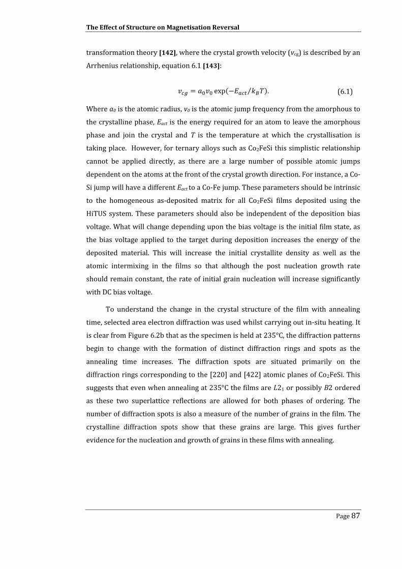
The Effect of Structure on Magnetisation Reversal
Page 87
transformation theory [142], where the crystal growth velocity (vcg) is described by an
Arrhenius relationship, equation 6.1 [143]:
( ⁄ ) (6.1)
Where a0 is the atomic radius, v0 is the atomic jump frequency from the amorphous to
the crystalline phase, Eact is the energy required for an atom to leave the amorphous
phase and join the crystal and T is the temperature at which the crystallisation is
taking place. However, for ternary alloys such as Co2FeSi this simplistic relationship
cannot be applied directly, as there are a large number of possible atomic jumps
dependent on the atoms at the front of the crystal growth direction. For instance, a Co-
Si jump will have a different Eact to a Co-Fe jump. These parameters should be intrinsic
to the homogeneous as-deposited matrix for all Co2FeSi films deposited using the
HiTUS system. These parameters should also be independent of the deposition bias
voltage. What will change depending upon the bias voltage is the initial film state, as
the bias voltage applied to the target during deposition increases the energy of the
deposited material. This will increase the initial crystallite density as well as the
atomic intermixing in the films so that although the post nucleation growth rate
should remain constant, the rate of initial grain nucleation will increase significantly
with DC bias voltage.
To understand the change in the crystal structure of the film with annealing
time, selected area electron diffraction was used whilst carrying out in-situ heating. It
is clear from Figure 6.2b that as the specimen is held at 235°C, the diffraction patterns
begin to change with the formation of distinct diffraction rings and spots as the
annealing time increases. The diffraction spots are situated primarily on the
diffraction rings corresponding to the [220] and [422] atomic planes of Co2FeSi. This
suggests that even when annealing at 235°C the films are L21 or possibly B2 ordered
as these two superlattice reflections are allowed for both phases of ordering. The
number of diffraction spots is also a measure of the number of grains in the film. The
crystalline diffraction spots show that these grains are large. This gives further
evidence for the nucleation and growth of grains in these films with annealing.
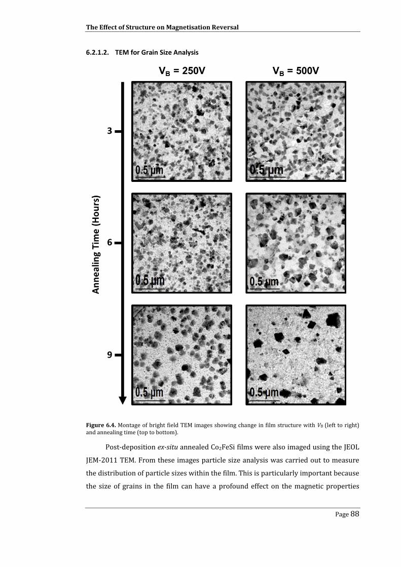
The Effect of Structure on Magnetisation Reversal
Page 88
6.2.1.2. TEM for Grain Size Analysis
Figure 6.4. Montage of bright field TEM images showing change in film structure with VB (left to right) and annealing time (top to bottom).
Post-deposition ex-situ annealed Co2FeSi films were also imaged using the JEOL
JEM-2011 TEM. From these images particle size analysis was carried out to measure
the distribution of particle sizes within the film. This is particularly important because
the size of grains in the film can have a profound effect on the magnetic properties

The Effect of Structure on Magnetisation Reversal
Page 89
[47]. The films deposited onto the carbon coated Cu TEM grids were imaged after
annealing at 500°C for 3, 6 and 9 hours. The change in the film structures with
deposition bias voltage and annealing time can be seen in Figure 6.4. It is clearly
observable, even without detailed analysis, that the films deposited at higher VB have
an increased average grain size. There is also a clear development of the grains with
annealing time. These films do however look significantly different to those annealed
in-situ. This is due to the difference in the annealing environment between the vacuum
of the TEM and the Ar atmosphere, as well as the rates of heating. The annealing
temperature was considered as the possible reason for this variation in film structure
but further studies of in-situ films showed that annealing at 500°C still did not
produce films similar to those shown in Figure 6.4.
Figure 6.5. Grain size distributions and example TEM images for HiTUS deposited Co2FeSi films with VB=250 V.

The Effect of Structure on Magnetisation Reversal
Page 90
It is immediately clear from the TEM images that the grain size of the Co2FeSi is
large when compared with typical films deposited using the HiTUS system [121]. The
images were all taken at a magnification of x12k. This is an extremely low
magnification for conventional TEM and a factor of 10 lower than that typically used
to image films deposited using the HiTUS system [122]. This means that the grains
have a diameter an order of magnitude larger, with grain sizes in the region of 40 nm –
200 nm. This immediately removes the majority of the grains from the single domain
particle regime which has a profound effect on the magnetisation reversal of these
films.
Figure 6.4 also shows a difference in how the films vary with annealing time.
After 3 hours of annealing the films look similar but after 9 hours of annealing they
are very different. For the sample grown with VB = 500 V there are a small number of
extremely large grains (~180 nm) which have most likely formed through coalescence
of neighbouring grains. The grains in the sample grown at a bias voltage of 250 V
however have a much greater number of grains with a smaller average diameter than
those seen in the sample grown at VB = 500 V. This is the result of the increase in the
number of initial crystallites in the film deposited with VB = 500 V. The initial
crystallite density in this film is greater so neighbouring grains coalesce. In the film
deposited with VB = 250 V the initial crystallite density is lower so the grain are too
sparsely distributed to coalesce.
Particle size analysis was performed on all the specimens. The diameters of over
800 grains were measured for each sample using an equivalent area method [144].
This was carried out using a Zeiss particle analyser, where a variable diameter light
spot can be fitted to the approximate area of each grain. The diameter of the light spot
is recorded as a voltage supplied to the bulb using a LabView VI routine. The
distribution of particle diameters can then be fitted to a lognormal distribution
function, described by equation 6.2, using the method outlined by O’Grady and
Bradbury [144].
( )
√ (
( ( ) )
)
(6.2)
where D is the measured particle diameter, and are the standard deviation
and the mean value of ln(D). The particle size analysis shows that the median particle
diameter in the film deposited with VB=250 V increases with annealing time. However

The Effect of Structure on Magnetisation Reversal
Page 91
an unusual trend is seen in the standard deviation. The decrease in to 0.26 after
annealing for 6 hours and subsequent increase to 0.36 after 9 hours is unusual. This
can be explained by a two stage growth mechanism. Up to 6 hours, new particles are
nucleating and previously nucleated particles are using material from the surrounding
matrix of Co, Fe and Si to continue growth via the process outlined in section 6.2.1.1
[143]. After 6 hours the majority of the film is crystallised and any subsequent growth
is facilitated by coalescence of neighbouring grains. This leads to the formation of
some extremely large grains and a number of much smaller grains remaining from
particles unable to coalesce. This would lead to an increased width of the distribution
as shown in Figure 6.5. A summary of the particle size analysis for the films grown at
different bias voltages is shown in Table 6.1.
Table 6.1. Summary of particle size analysis data for HiTUS deposited Co2FeSi thin films.
VB (V)
TA (Hours)
Dm (± 1 nm)
σlnD
(±0.05)
3 54 0.34 250 6 60 0.26
9 63 0.36
3 78 0.46 500 6 75 0.32
9 72 0.40
3 79 0.44 750 6 84 0.35
9 75 0.35
A general trend of increasing grain size with VB is immediately observable,
particularly for the films annealed for 6 hours. This confirms that the initial film
deposition conditions have a larger effect on the final structure of the film than any
annealing carried out, beyond that which facilitates the initial crystallisation of the as-
deposited film. This is due to the mobility of the constituent elements to form the
complex L21 phase. The data in Table 6.1 also shows that for the samples deposited at
750 V the grain size begins to decrease when the samples are annealed for 9 hours. In
Co2MnSi films created under similar conditions this has been explained as being due
to Si segregation from the ordered grains [123]. It can however be seen that for the
film deposited with VB = 250 V, this trend is not followed. The grain size in these films
is still much smaller than that for the films deposited with VB=500 V and VB = 750 V.
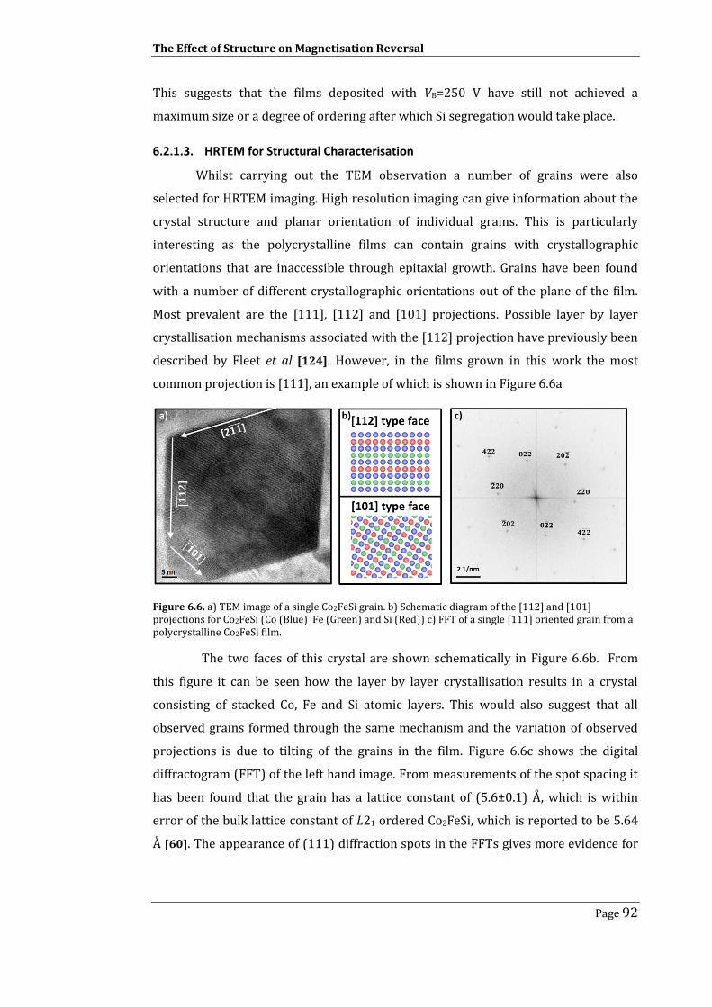
The Effect of Structure on Magnetisation Reversal
Page 92
This suggests that the films deposited with VB=250 V have still not achieved a
maximum size or a degree of ordering after which Si segregation would take place.
6.2.1.3. HRTEM for Structural Characterisation
Whilst carrying out the TEM observation a number of grains were also
selected for HRTEM imaging. High resolution imaging can give information about the
crystal structure and planar orientation of individual grains. This is particularly
interesting as the polycrystalline films can contain grains with crystallographic
orientations that are inaccessible through epitaxial growth. Grains have been found
with a number of different crystallographic orientations out of the plane of the film.
Most prevalent are the [111], [112] and [101] projections. Possible layer by layer
crystallisation mechanisms associated with the [112] projection have previously been
described by Fleet et al [124]. However, in the films grown in this work the most
common projection is [111], an example of which is shown in Figure 6.6a
Figure 6.6. a) TEM image of a single Co2FeSi grain. b) Schematic diagram of the [112] and [101] projections for Co2FeSi (Co (Blue) Fe (Green) and Si (Red)) c) FFT of a single [111] oriented grain from a polycrystalline Co2FeSi film.
The two faces of this crystal are shown schematically in Figure 6.6b. From
this figure it can be seen how the layer by layer crystallisation results in a crystal
consisting of stacked Co, Fe and Si atomic layers. This would also suggest that all
observed grains formed through the same mechanism and the variation of observed
projections is due to tilting of the grains in the film. Figure 6.6c shows the digital
diffractogram (FFT) of the left hand image. From measurements of the spot spacing it
has been found that the grain has a lattice constant of (5.6±0.1) Å, which is within
error of the bulk lattice constant of L21 ordered Co2FeSi, which is reported to be 5.64
Å [60]. The appearance of (111) diffraction spots in the FFTs gives more evidence for

The Effect of Structure on Magnetisation Reversal
Page 93
the grains in the film being L21 ordered as these spots are known to diminish for
disordered phases of Co2FeSi [145].
6.2.2. Epitaxially Sputtered Films
6.2.2.1. X-ray Diffraction
Detailed structural analysis has been carried out on the epitaxial sputtered
films using X-ray diffraction (XRD). 2θ/ω (out of plane) and φ ((111) plane) scans
have been carried out for all the epitaxial films and are shown in Figure 6.7. The 2θ/ω
scan can give an indication of increasing L21 ordering but this cannot be confirmed
without the φ scan, as the [200] and [400] superlattice reflections observable in
Figure 6.7a are common to both the L21 and B2 phases of Co2FeSi. The (111) reflection
is only allowed for L21 ordering [145].
Figure 6.7. a) 2θ/ω and b) φ ((111) plane) XRD scans for epitaxially sputtered Co2FeSi films deposited on MgO(001) substrates.

The Effect of Structure on Magnetisation Reversal
Page 94
Figure 6.7a shows increasing intensity of both the (002) and (004)
superlattice reflections with annealing temperature. These peaks are also seen to
become sharper with annealing which means that not only is there a larger degree of
B2 or L21 ordering but that the size of these regions is increasing. Figure 6.7b confirms
the presence of L21 ordering in these films due to the presence of (111) diffraction
peaks. The intensity and sharpness of these peaks is seen to increase dramatically
with annealing temperature, showing that the film is becoming predominantly L21
ordered. Widespread L21 ordering is observed in the films annealed at 600°C. To
quantify the extent of this ordering, an approximation of the size of the ordered
regions has been made using Scherrer’s formula (equation 4.6) using the FWHM of the
(111) peaks in the φ scan [130]. In the as-deposited films, it was found that the L21
ordered regions extended an average of (70±15) nm without a change of phase. This
increased to (180±10) nm for the sample annealed at 500°C and reached (374±8) nm
for the sample annealed at 600°C. The decreasing error on these measurements is an
estimation of the accuracy to which the FWHM can be measured. This final result for
the sample annealed at 600°C is particularly important as the grain size is much
greater than the typical dimensions for a nano-pillar device, typically 75 - 200 nm
diameter [42]. As a result, devices made from films such as these are unlikely to have
any changes of ordering within the volume of the Co2FeSi layers. This would mean
that the bulk spin polarisation and magnetic characteristics are constant in each of the
ferromagnetic layers of the device.
6.2.2.2. HRSTEM Observation of Atomic Ordering and Film Interfaces
To confirm the degree and nature of the ordering a large amount of TEM and
STEM analysis was performed. Specimens were imaged at high magnification after
preparing film cross sections using the mechanical thinning method described in [35].
The specimens were then imaged using the JEOL JEM-2200FS STEM. This allows
direct imaging of the ordering in the film. This is shown in Figure 6.8a.
The film was imaged along the (100) plane resulting in an image of the (110)
face of the Co2FeSi. A schematic of the atomic structure of this face is shown overlaid
on the image. When compared to the HRSTEM image it is clear that this region of the
film is L21 ordered. The brightest spots correspond to the rows of Co, whilst the
alternating bright and dark spots correspond to the Fe and Si respectively. The
intensity of the Fe spots is diminished from that of the Co due to the alternating Fe and
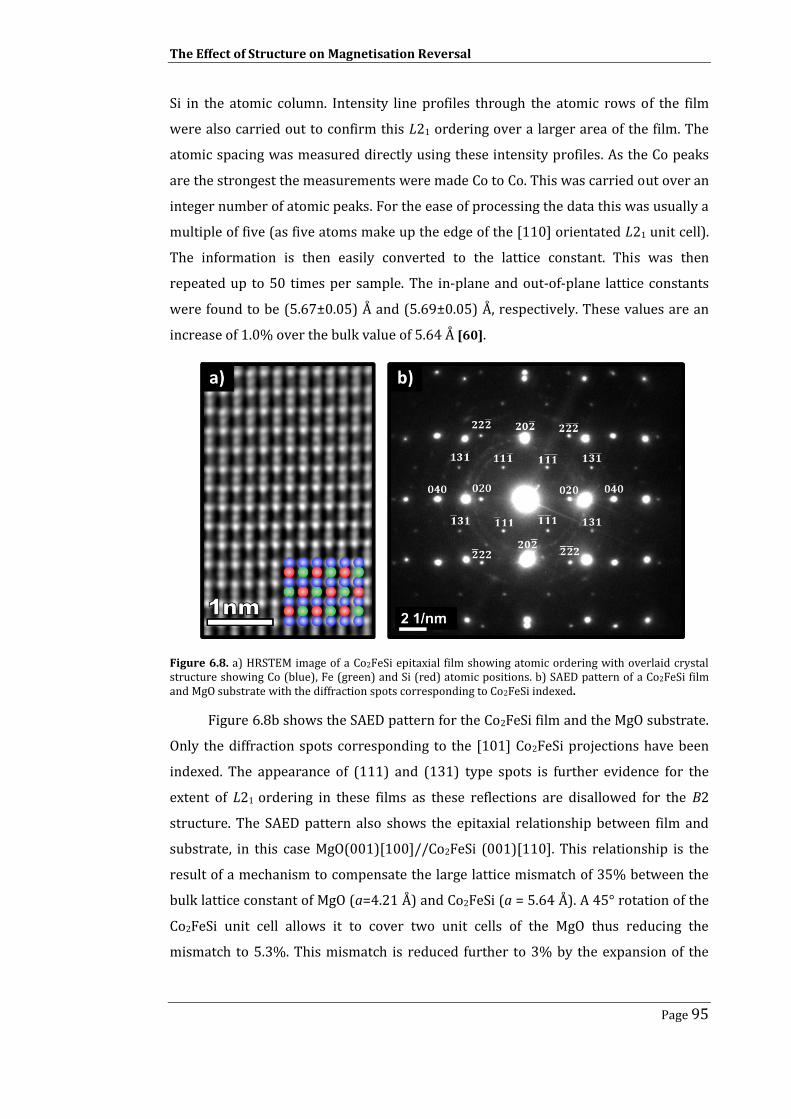
The Effect of Structure on Magnetisation Reversal
Page 95
Si in the atomic column. Intensity line profiles through the atomic rows of the film
were also carried out to confirm this L21 ordering over a larger area of the film. The
atomic spacing was measured directly using these intensity profiles. As the Co peaks
are the strongest the measurements were made Co to Co. This was carried out over an
integer number of atomic peaks. For the ease of processing the data this was usually a
multiple of five (as five atoms make up the edge of the [110] orientated L21 unit cell).
The information is then easily converted to the lattice constant. This was then
repeated up to 50 times per sample. The in-plane and out-of-plane lattice constants
were found to be (5.67±0.05) Å and (5.69±0.05) Å, respectively. These values are an
increase of 1.0% over the bulk value of 5.64 Å [60].
Figure 6.8. a) HRSTEM image of a Co2FeSi epitaxial film showing atomic ordering with overlaid crystal structure showing Co (blue), Fe (green) and Si (red) atomic positions. b) SAED pattern of a Co2FeSi film and MgO substrate with the diffraction spots corresponding to Co2FeSi indexed.
Figure 6.8b shows the SAED pattern for the Co2FeSi film and the MgO substrate.
Only the diffraction spots corresponding to the [101] Co2FeSi projections have been
indexed. The appearance of (111) and (131) type spots is further evidence for the
extent of L21 ordering in these films as these reflections are disallowed for the B2
structure. The SAED pattern also shows the epitaxial relationship between film and
substrate, in this case MgO(001)[100]//Co2FeSi (001)[110]. This relationship is the
result of a mechanism to compensate the large lattice mismatch of 35% between the
bulk lattice constant of MgO (a=4.21 Å) and Co2FeSi (a = 5.64 Å). A 45° rotation of the
Co2FeSi unit cell allows it to cover two unit cells of the MgO thus reducing the
mismatch to 5.3%. This mismatch is reduced further to 3% by the expansion of the

The Effect of Structure on Magnetisation Reversal
Page 96
Co2FeSi in-plane lattice spacing to the previously measured (5.67±0.05) Å and a
contraction of the MgO lattice constant to (4.13±0.05) Å at the interface, as found from
the HRSTEM.
The effect of this mismatch at the interface has been further investigated using
weak-beam dark-field imaging in the JEOL JEM-2010. By imaging selectively from the
MgO(020) diffraction spots, it is possible to highlight a periodic contrast variation at
the film/substrate interface (Figure 6.9a). This is a result of atomic planes bending
away from the imaging axis around misfit dislocation cores which appear to relieve
the stress caused by the remaining 3% lattice mismatch. Using the HRSTEM it is
possible to resolve these misfit dislocations and their effect on the structure of the
film/substrate interface. Figure 6.9b shows this HRSTEM image of the interface whilst
Figure 6.9c is a filtered image showing only the (020) planes. Superimposed onto this
is a strain map created using geometric phase analysis (GPA) from the FRWRtools
digital micrograph plug-in [146].
Figure 6.9. a) Weak-beam dark-field image of the Co2FeSi/MgO interface. b) HRSTEM image of a similar region of the Co2FeSi/MgO interface. c) Co2FeSi/MgO interface image filtered using the (020) spots in the FFT, with superimposed strain map and highlighted dislocation cores.
GPA is based on the analysis of the phase components of the spatial frequencies
which form HRSTEM images. By masking two selected Bragg spots in the Fourier
transform the phases of the selected spatial frequencies can be measured. The phases
of the two images can then be compared relative to one another to create a strain map

The Effect of Structure on Magnetisation Reversal
Page 97
across the image. An area in the image is selected as a reference from which the
relative distortion of spatial frequencies can be measured. A full discussion of the
theoretical foundation of GPA can be found in reference [147]. To form Figure 6.9c, a
region of the MgO away from the interface was chosen as the reference. This strain
map highlights the cores of the dislocations at the interface and shows that these
occur due to the epitaxy missing a single plane of every 20-25 MgO atomic planes. The
GPA also shows that away from the interface the Co2FeSi film becomes fully relaxed
with a lattice mismatch of (4.4±1.0)% relative to the MgO substrate.
These films have been shown to have a considerably different structure to that
found in the polycrystalline thin films. Samples annealed at 600°C show long range
L21 ordering in the XRD measurements. This was confirmed using HRSTEM to image
directly the atomic ordering. This is in contrast to the granular structure found in the
polycrystalline films. The single crystal films also have a specific planar orientation
defined by the epitaxy between substrate and film unlike the distributed orientations
seen in the granular films. This epitaxy relationship does however result in a periodic
array of misfit dislocation at the film/substrate interface which could potentially act
as domain wall pins.
6.3. Magnetic Properties
6.3.1. Hysteresis
The measurement that allows the most obvious comparison of the magnetic
properties of the magnetron and HiTUS sputtered films is the hysteresis loop. This
allows for a comparison of coercivity (Hc), remanence (Mr) and nucleation field (Hn). A
relative comparison can also be drawn for saturation magnetisation (Ms), although as
these measurements are taken using the AGFM this value is dependent upon the
characteristics of the probe and the sample dimensions, as discussed in section 5.1.1.
The error in the reproducibility of a single measurement of Ms for a specific sample
was shown by Lewis [148] to be 5.4%. This does not include any factors arising from
the variation in shape, size and mass of samples or probes. Hence, it should be
considered impossible to measure Ms with an accuracy of better than 10%. Therefore,
most measurements are shown with the normalised or reduced moment M/Ms. any
direct measurements of Ms have been carried out using the VSM as these

The Effect of Structure on Magnetisation Reversal
Page 98
measurements are not probe dependent, although they are made relative to a
calibration sample.
As previously discussed (section 4.1.1), the HiTUS system controls film
deposition through the strength of a DC bias applied to the sputter target. This
changes the deposition rate and film structure which has an extremely large effect on
the hysteresis of the films. Thus, the films have been characterised both by VB and
annealing time (TA) as shown in Figure 6.10.
Figure 6.10. Hysteresis loops for polycrystalline Co2FeSi films deposited at DC bias voltages of 250 V and 750 V, annealed at 500°C for 3, 6, and 9 hours.

The Effect of Structure on Magnetisation Reversal
Page 99
It is shown quite clearly that VB has a larger effect on the magnetic properties
of the thin film than the annealing time, where increasing VB results in a monotonic
increase in Hc. Annealing time also shows a somewhat different variation in magnetic
properties. The main difference seen in Figure 6.10 is in the shape of the hysteresis
loops. The magnetisation reversal of specimens grown with a DC bias of 250 V is
dominated by a single process. In contrast, the film deposited with the higher bias of
750 V shows a clearly defined two stage reversal process. Importantly the hysteresis
loops for the specimen deposited with VB =250 V and annealed for 3 and 9 hours have
Mr/Ms = 0.85 and 0.87. This suggests that the grains in these films exhibit a cubic
structure with a 3D random distribution of easy axes. Hysteresis loops for such
systems were initially modelled by Gans [149]. The model was extended to include the
entire reversal process by Joffe and Heuberger [150]. This model is based upon the
assumption that the magnetisation reversal process takes place through coherent
rotation of the spins through the material. If the reversal process becomes incoherent
this model breaks down. Both these references predict Mr/Ms = 0.83 - 0.87 dependent
upon the magneto-crystalline anisotropy of the material, which is in good agreement
with the results presented here. The intermediate stage of annealing at 6 hours
represents an intermediate step in grain development where growth and re-
crystallisation result in a decrease in Mr and an increase in Hc. This is due to
hindrances to the rotation of spins through the cubic crystals occurring as a result of
the re-crystallisation process.
The hysteresis loops for the sample deposited with VB = 750 V are very
different, with the initial reversal taking place at a relatively small reverse field (~400
Oe) and reversing almost 70% of the material, the remaining 30% then takes a much
larger reverse field to fully saturate (HMs = 4500 Oe). This two stage reversal can be
seen in all samples to varying degrees. The amount of material reversing via the
second process increases with annealing time. These films also show lower values of
Mr/Ms. This is an indication that the structure within the grains has changed to
prevent coherent reversal of the magnetisation. This, as well as the increasing
secondary reversal stage, is most likely due to increased grain volume allowing the
formation of domain walls within the grain. A summary of the measured quantities
from all the samples studied is shown in Table 6.2.
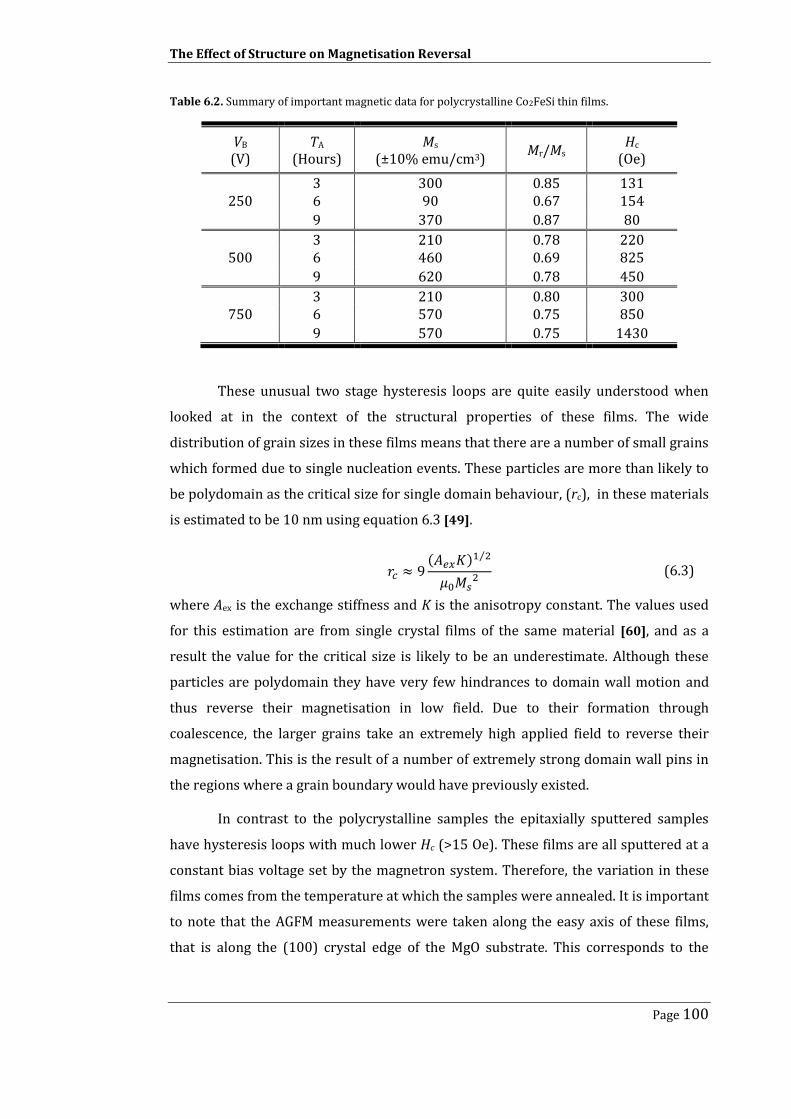
The Effect of Structure on Magnetisation Reversal
Page 100
Table 6.2. Summary of important magnetic data for polycrystalline Co2FeSi thin films.
VB (V)
TA (Hours)
Ms (±10% emu/cm3)
Mr/Ms Hc
(Oe)
3 300 0.85 131 250 6 90 0.67 154
9 370 0.87 80
3 210 0.78 220 500 6 460 0.69 825
9 620 0.78 450
3 210 0.80 300 750 6 570 0.75 850
9 570 0.75 1430
These unusual two stage hysteresis loops are quite easily understood when
looked at in the context of the structural properties of these films. The wide
distribution of grain sizes in these films means that there are a number of small grains
which formed due to single nucleation events. These particles are more than likely to
be polydomain as the critical size for single domain behaviour, (rc), in these materials
is estimated to be 10 nm using equation 6.3 [49].
( )
⁄
(6.3)
where Aex is the exchange stiffness and K is the anisotropy constant. The values used
for this estimation are from single crystal films of the same material [60], and as a
result the value for the critical size is likely to be an underestimate. Although these
particles are polydomain they have very few hindrances to domain wall motion and
thus reverse their magnetisation in low field. Due to their formation through
coalescence, the larger grains take an extremely high applied field to reverse their
magnetisation. This is the result of a number of extremely strong domain wall pins in
the regions where a grain boundary would have previously existed.
In contrast to the polycrystalline samples the epitaxially sputtered samples
have hysteresis loops with much lower Hc (>15 Oe). These films are all sputtered at a
constant bias voltage set by the magnetron system. Therefore, the variation in these
films comes from the temperature at which the samples were annealed. It is important
to note that the AGFM measurements were taken along the easy axis of these films,
that is along the (100) crystal edge of the MgO substrate. This corresponds to the

The Effect of Structure on Magnetisation Reversal
Page 101
(110) direction of Co2FeSi as per the epitaxial relationship shown in Figure 6.11. It
should therefore follow that taking a measurement at 90° to this direction would also
produce an easy axis loop. By measuring Mr/Ms as a function of the applied field angle
it can be seen that the easy axis corresponds to the (110) direction of Co2FeSi,
however at 90° a value of Mr/Ms = 1 is not achieved. This is due to the presence of a
small applied field (<100 Oe) during the annealing process from the remanent
magnetisation of the pole pieces of the magnet in which the furnace was situated.
Figure 6.11 Schematic diagram of epitaxial relationship between MgO and Co2FeSi with the resulting crystallographic directions and the effect on the anisotropy.
This applied field during annealing induces an extra anisotropy in the
direction of the field (110) which must be overcome when measuring along the ( )
direction. This applied magnetic field during annealing results in a change in the cubic
symmetry of the exchange interaction in the lattice. This results in an offset of domain
wall energy therefore stabilising the domain walls in the easy direction. This induced
anisotropy behaviour has been documented in cubic materials since 1955 [151]. This
stabilisation results in the change in remanence observed between the measurements
along the (110) and ( ) directions, as the increased anisotropy reduces the
susceptibility of the film to nucleation of reverse domains due to thermal activation.
Costa-Kramer et al. [152] observed similar behaviour in 20 nm thick Fe films grown on
MgO(001) which was explained by a change of domain wall type in the films. The
magnetisation reversal along the induced easy axis (110) is through the nucleation
and propagation of 180° domain walls, whilst along the ( ) direction the reversal
process is facilitated through the nucleation and propagation of 90° domain walls.
Another feature of the angular dependence is a small peak at an applied field angle of
45°, corresponding to the (100) direction of the Co2FeSi. This result is analogous to
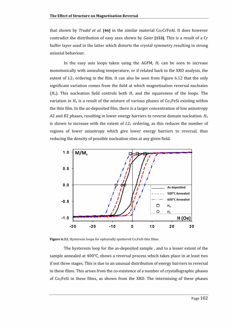
The Effect of Structure on Magnetisation Reversal
Page 102
that shown by Trudel et al. [46] in the similar material Co2CrFeAl. It does however
contradict the distribution of easy axes shown by Gaier [153]. This is a result of a Cr
buffer layer used in the latter which distorts the crystal symmetry resulting in strong
uniaxial behaviour.
In the easy axis loops taken using the AGFM, Hc can be seen to increase
monotonically with annealing temperature, or if related back to the XRD analysis, the
extent of L21 ordering in the film. It can also be seen from Figure 6.12 that the only
significant variation comes from the field at which magnetisation reversal nucleates
(Hn). This nucleation field controls both Hc and the squareness of the loops. The
variation in Hn is a result of the mixture of various phases of Co2FeSi existing within
the thin film. In the as-deposited film, there is a larger concentration of low anisotropy
A2 and B2 phases, resulting in lower energy barriers to reverse domain nucleation. Hn
is shown to increase with the extent of L21 ordering, as this reduces the number of
regions of lower anisotropy which give lower energy barriers to reversal, thus
reducing the density of possible nucleation sites at any given field.
Figure 6.12. Hysteresis loops for epitaxially sputtered Co2FeSi thin films.
The hysteresis loop for the as-deposited sample , and to a lesser extent of the
sample annealed at 400°C, shows a reversal process which takes place in at least two
if not three stages. This is due to an unusual distribution of energy barriers to reversal
in these films. This arises from the co-existence of a number of crystallographic phases
of Co2FeSi in these films, as shown from the XRD. The intermixing of these phases

The Effect of Structure on Magnetisation Reversal
Page 103
results in areas of the film with lower magneto-crystalline anisotropy which reduces
the energy barrier to reversal so reverse domains can nucleate at lower reverse field.
These regions have such low energy barriers that they are thermally unstable at room
temperature. This is shown by values of Mr/Ms that are less than 1 for these films.
The distribution of reversible and irreversible magnetisation reversal steps for
the as-deposited film and the film annealed at 500°C would be distinctly bi-modal. The
first peak is due to disordered material where reverse domains can nucleate easily,
while the larger second peak is the reversal of the remaining well-ordered film by
domain wall motion. For the bi-modal distributions, the blocking temperature (TB) for
these films lies within the distribution. TB is the temperature above which magnetic
entities will become superparamagnetic. For uniaxial single domain particles this is
given by equation 6.4 [47]:
( ⁄ )
(6.4)
Where K is the anisotropy constant for the material and V is the volume of the particle.
The factor 25 is a direct result of the typical measurement time of 100 seconds. For
epitaxially sputtered single crystal cubic films such as these this will not hold exactly.
However, it does show that this superparamagnetic behaviour of the regions within
this film will be controlled by both the volume of the region and the anisotropy.
Therefore, any regions of the low anisotropy A2 phase of Co2FeSi or the amorphous
as-deposited matrix will most likely result in superparamagnetic regions in the film.
This is due to both the low anisotropy and the small volume of these regions.
6.3.2. DCD Curves
As the first stage to understanding the reversal processes in both the
polycrystalline and epitaxial films, DC demagnetised (DCD) remanence curves have
been measured for all the specimens. As previously discussed in chapters 2 and 5
remanence curves give a great detail of understanding about the fundamentals of the
magnetisation reversal process as they measure only the irreversible component of
the magnetisation at any given field. Because of the need to differentiate these curves
to find χirr, which is needed for the estimation of Vact, it is crucial that the noise in the
measurement is limited as it will be amplified when taking the gradient between two
points. To remove any noise from the measurement, the data is smoothed using a five
point moving quadratic as described in section 5.1.3. The DCD curves for an epitaxial

The Effect of Structure on Magnetisation Reversal
Page 104
film and a polycrystalline film are shown in Figure 6.13. Both DCD curves are shown
with the specimens’ hysteresis loop for ease of comparison.
The data in Figure 6.13 shows that the two film structures have fundamentally
different reversal mechanisms. Figure 6.13a shows the DCD curve from the
polycrystalline film. Here the DCD curve follows the hysteresis loop until 800 Oe at
which point the DCD curve diverges from the hysteresis loop at a much greater rate.
This suggests that there are two different mechanisms in the reversal process. At
fields below 800 Oe the magnetisation reversal is controlled by domain nucleation
and growth within the ordered cores of the grains which nucleated during the initial
annealing process. Above 800 Oe much stronger domain wall pins exist which require
much greater fields to overcome. These domain wall pins most likely form during the
coalescence phase of the grain growth. The film also contains a large number of
thermally unstable grains, shown by the difference in moment between the hysteresis
loop at saturation and the DCD curve at the same field. Almost 25% of the saturation
moment can be attributed to these grains, which consist of the material from the as
deposited matrix which has failed to crystallise.
Figure 6.13. Hysteresis loops (black) and DCD remanence curves (red) for a) a polycrystalline Co2FeSi film deposited with VB=750 V and annealed at 500°C for 6 hours and b) an epitaxially sputtered Co2FeSi film annealed at 600°C for 1 hour.
In Figure 6.13b, for the epitaxially sputtered film the DCD curve follows the
hysteresis almost exactly, suggesting a single reversal mechanism consisting of
entirely irreversible processes. This behaviour is consistent with a series of
periodically spaced low energy domain wall pins which must be overcome in turn to
reverse the magnetisation of the entire sample. The previously discussed misfit

The Effect of Structure on Magnetisation Reversal
Page 105
dislocations at the film/substrate interface are a possible origin of this periodic
pinning.
6.3.3. Activation Volumes
Measurements of magnetic time dependence have been made for all the
samples, allowing access to the magnetic viscosity coefficients which are needed for
calculation of the activation volume (Vact). The decay of magnetisation was measured
at 150 points over 600 seconds for each field step. All the decay curves have been
found to be linear in ln(t), a small selection of these can be seen in Figure 6.14b.
Because of this, the fluctuation field (Hf) and hence Vact can be obtained through the
S(H)/χirr(H) method using equations 6.5 and 6.6 [154].
(6.5)
( )
( )
(6.6)
Figure 6.14a shows the S(H) and χirr curves for a polycrystalline Co2FeSi film
annealed for 9 hours. The χirr curve is noticeably bi-model as is the S(H) curve. This is
a result of the previously discussed two phase reversal process. It must also be noted
that not all the polycrystalline specimens exhibit such behaviour. It is therefore
important to remain consistent when describing the activation volume. As all the
samples exhibit the initial nucleation phase of the reversal the measurement of the
activation volume will take place in this part of the process indicated by the first peak
in the χirr curve shown in Figure 6.14a.
Vact calculated in this way, (for all polycrystalline specimens) can be seen in
Table 6.3. The measured value of saturation moment has been used for each sample
after calibrating the AGFM probe before each measurement. The saturation
magnetisation has been calculated by setting the volume of the film equal to the film
thickness multiplied by the area of substrate covered by the film. In the case of these
specimens the film covered 100% of the substrate surface.

The Effect of Structure on Magnetisation Reversal
Page 106
Figure 6.14. a) S(H)(black circles) and χirr(H) (red line) curves for a polycrystalline Co2FeSi sample deposited at VB=750 V and annealed at 500°C for 9 hours. b) The magnetisation decay curves for the highlighted region (dashed box) in S(H) above.
For ease of comparison Vact has been converted to an activation diameter
(Dact). Dact is calculated by modelling Vact as a cylinder through the film thickness. It is
immediately clear that the values of Dact remain almost constant with both VB and TA.
This suggests that the initial nucleation process in each film takes place from the same
volume of magnetic material. Where the films then begin to differ is in the subsequent
reversal process, resulting in the extremely large coercivities (Hc) and saturation
fields (HMS) seen for some films (Table 6.2), whilst others remain very low.

The Effect of Structure on Magnetisation Reversal
Page 107
Table 6.3. Summary of activation volume data for polycrystalline Co2FeSi thin films.
VB (V)
TA (Hours)
Ms (±10%
emu/cm3)
χirr(H) (±0.1 x 10⁻⁷)
S(H) (±1 x 10⁻⁷)
Vact (x10-18 cm3)
Dact (±2 nm)
3 300 11 46 33 45 250 6 90 3 28 53 58
9 370 19 80 26 41
3 210 5 33 29 43 500 6 460 4 8 43 52
9 620 10 16 43 53
3 210 7 42 34 47 750 6 570 6 9 52 58
9 570 4 10 31 45
For the epitaxially sputtered films, the activation volumes have been found to
be much smaller with Dact ~5 nm for all films irrespective of annealing time. The
magnetic viscosity and χirr curves also show significantly different trends to those in
the polycrystalline films. Both χirr and S(H) exhibit a strong peaked behaviour as
shown in Figure 6.15. None of the samples show bimodal behaviour of χirr(H) as one
may expect from simply observing the hysteresis loops. This means that the two stage
reversal shown in the hysteresis loops (Figure 6.12) is a product of reversible
processes in the film.
Figure 6.15. S(H) (red line) and χirr(H) (black circles) for an epitaxially sputtered Co2FeSi sample annealed at 600°C.
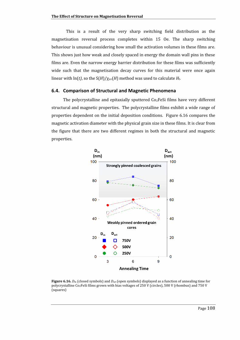
The Effect of Structure on Magnetisation Reversal
Page 108
This is a result of the very sharp switching field distribution as the
magnetisation reversal process completes within 15 Oe. The sharp switching
behaviour is unusual considering how small the activation volumes in these films are.
This shows just how weak and closely spaced in energy the domain wall pins in these
films are. Even the narrow energy barrier distribution for these films was sufficiently
wide such that the magnetisation decay curves for this material were once again
linear with ln(t), so the S(H)/χirr(H) method was used to calculate Hf.
6.4. Comparison of Structural and Magnetic Phenomena
The polycrystalline and epitaxially sputtered Co2FeSi films have very different
structural and magnetic properties. The polycrystalline films exhibit a wide range of
properties dependent on the initial deposition conditions. Figure 6.16 compares the
magnetic activation diameter with the physical grain size in these films. It is clear from
the figure that there are two different regimes in both the structural and magnetic
properties.
Figure 6.16. Dm (closed symbols) and Dact (open symbols) displayed as a function of annealing time for polycrystalline Co2FeSi films grown with bias voltages of 250 V (circles), 500 V (rhombus) and 750 V (squares)

The Effect of Structure on Magnetisation Reversal
Page 109
The films deposited using a DC bias voltage of 250 V have grain volumes roughly
equal to the magnetic activation volumes. This suggests that these particles exhibit
either single domain particle behaviour, where the reversal occurs through rotation of
the magnetisation in the grain, or more likely, that reverse domains nucleate in the
film, and the ordered grains can switch coherently due to very few domain wall pins.
For the films grown at high VB the same nucleation event occurs in these ordered
‘core’ grains. However, due to the large proportion of coalesced grains, there are a
much higher density of strong domain wall pins at the grain boundaries where
material becomes magnetically disordered. A much larger reverse field is then
required to sweep out these domain wall pins.
Figure 6.17. DXRD (squares), Dact (rhombuses) and Ddefect (circles) displayed as a function of annealing temperature for epitaxially sputtered Co2FeSi films.
The story for the epitaxial films is much different. From the XRD results it is
shown that these films are well ordered over extremely long ranges (>80 nm).
Furthermore, the size of ordered regions increases with annealing temperature.
However, the activation volumes are considerably smaller than the ordered regions
and show very little temperature dependence. This means that the initial nucleation
event is controlled by a number of magnetically soft disordered regions in the film,
The Effect of Structure on Magnetisation Reversal
Page 110
whilst the subsequent reversal mechanism is controlled by another structural
property. By converting the activation volumes to an activation diameter more insight
into the source of this domain wall pinning can be found. This is shown in Figure 6.17
where the size of the ordered regions (DXRD) and Dact are shown relative to one
another. Dact is coincident within error of the mean spacing of misfit dislocation at the
film/substrate interface. This suggests that the reversal mechanism in these epitaxial
films is controlled by the distribution of structural defects.
It has been shown that the structure of these Co2FeSi films have a profound
effect on their magnetisation reversal. The polycrystalline films show a magnetisation
reversal process dominated by the initial deposition conditions which control the
number of ordered grain nucleation events, subsequently controlling the grain
development process and amount and strength of domain wall pins in the material.
The epitaxial films however have a magnetisation reversal process controlled by the
defects that occur due to epitaxial growth. This is of particular importance as this
domain wall pinning limits the rate at which magnetisation switching can occur. This
may make epitaxial tunnel barrier devices unsuitable for high frequency applications.
However, the effect of this could be removed by choosing specific material systems
with no lattice mismatch, thus removing the majority of these misfit dislocations.

The Effect of Seed Layers on Polycrystalline Films
Page 111
Chapter 7. The Effect of Seed Layers on Polycrystalline Films
By depositing layers between the substrate and subsequent magnetic layers the
crystallographic structure and growth processes of thin films can be controlled. The
effect that these seed layers have on the structure and magnetic properties of Co2FeSi
polycrystalline films has been studied. Initially, Ag seed layers have been tested
because Ag is commonly used as the bottom electrode in nanopillar devices. This
study has then been extended to multiple seed layers, as well as antiferromagnetic
seed layers to induce an exchange bias in the Heusler alloy films.
7.1. Film Preparation
Thin film samples with structure Ag (6 nm)/Co2FeSi (20 nm)/Ru (3 nm) were
deposited onto single crystal Si and MgO (001) substrates as well as carbon coated
copper TEM grids, using a HiTUS sputtering system with a base pressure better than
4x10⁻⁵ Pa. Films have been deposited using DC bias voltages of 250 V, 400 V, 550 V,
700 V, 850 V and 990 V. The bias voltage in the HiTUS system controls the energy of
ions bombarding the sputter target, this changes the growth rate and subsequent
grain size in the sputtered films [122]. The films have been post-deposition ex-situ
annealed for 3, 6 and 9 hours at 300°C in a vacuum better than 3x10⁻³ Pa. As with the
specimens described in the previous chapter, the post deposition annealing facilitates
the growth of grains from the as-deposited matrix. However, due to the Ag seed layer,
this initial as-deposited state is no longer superparamagnetic. A number of regions
form larger initial crystallites which contribute to a small magnetic hysteresis of Hc ≤
10 Oe for all specimens.

The Effect of Seed Layers on Polycrystalline Films
Page 112
7.2. Magnetic Characterisation
Hysteresis loops have been measured for all specimens after annealing. These
specimens all show low coercivities of less than 40 Oe. This result is itself significant
over the previously studied films deposited without seed layers. For spintronic
devices where fast, coherent, magnetisation reversal is required, a low coercivity is
essential. In the previous study no film exhibited a coercivity of less than 80 Oe. Two
examples of the hysteresis loops for these films are shown in Figure 7.1. It is
immediately apparent that these films have a very different magnetic reversal process
than those previously discussed. These hysteresis loops are extremely square in shape
suggesting that the reversal process is dominated by a single nucleation event which
reverses the majority of the material in the film.
Figure 7.1. Typical M-H hysteresis loops for specimens deposited with VB=250 V (solid line) and VB=700 V (dashed line).
Figure 7.2 shows that increasing the deposition bias voltage results in an
increase in Hc. This is not a consistent trend since after 700 V there is a drastic
decrease, as shown in Figure 7.2a. At some point the structure of the films changes to
such a degree that the coercivity is reduced to less than 10 Oe. This suggests that for
the specimen deposited with VB = 990 V there is a significant change to either the
crystalline or morphological structure. The same trend however is not echoed in the
data for the saturation magnetisation. Here, there is a monotonic increase in Ms with
VB, which is almost linear as shown in Figure 7.2b. This means that either there is now
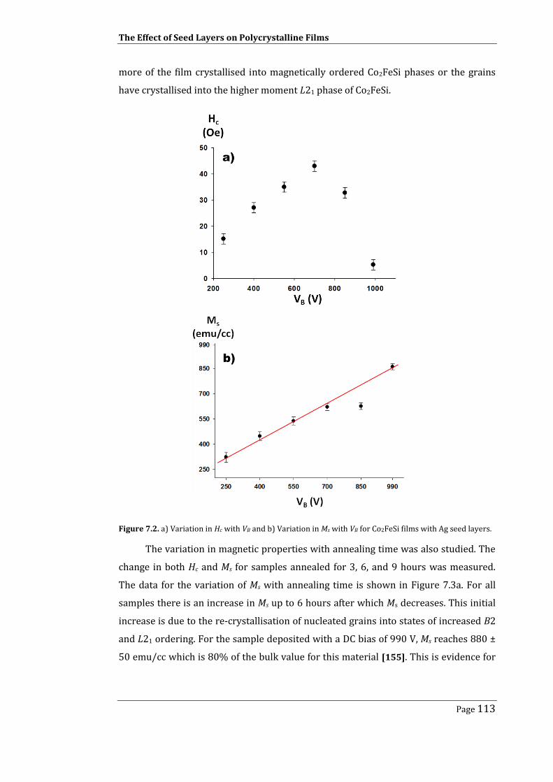
The Effect of Seed Layers on Polycrystalline Films
Page 113
more of the film crystallised into magnetically ordered Co2FeSi phases or the grains
have crystallised into the higher moment L21 phase of Co2FeSi.
Figure 7.2. a) Variation in Hc with VB and b) Variation in Ms with VB for Co2FeSi films with Ag seed layers.
The variation in magnetic properties with annealing time was also studied. The
change in both Hc and Ms for samples annealed for 3, 6, and 9 hours was measured.
The data for the variation of Ms with annealing time is shown in Figure 7.3a. For all
samples there is an increase in Ms up to 6 hours after which Ms decreases. This initial
increase is due to the re-crystallisation of nucleated grains into states of increased B2
and L21 ordering. For the sample deposited with a DC bias of 990 V, Ms reaches 880 ±
50 emu/cc which is 80% of the bulk value for this material [155]. This is evidence for

The Effect of Seed Layers on Polycrystalline Films
Page 114
increasing amounts of L21 and B2 ordering in the grains as the film is unlikely to be
100% crystalline. After 6 hours Ms decreases for all samples. This is due to segregation
of Si from these ordered grains, which was discussed in the previous chapter and
reported for a similar material, Co2MnSi [123].
Figure 7.3. Graphs showing the variation of a) Ms and b) Hc with annealing time for films deposited with VB = 250 V, 700 V and 990 V.
What is more interesting is the lack of variation in Hc shown in Figure 7.3b. This
suggests that the seed layer has constrained the grain size of the Co2FeSi layer such
that the distribution of energy barriers in this film remains constant with annealing
time.
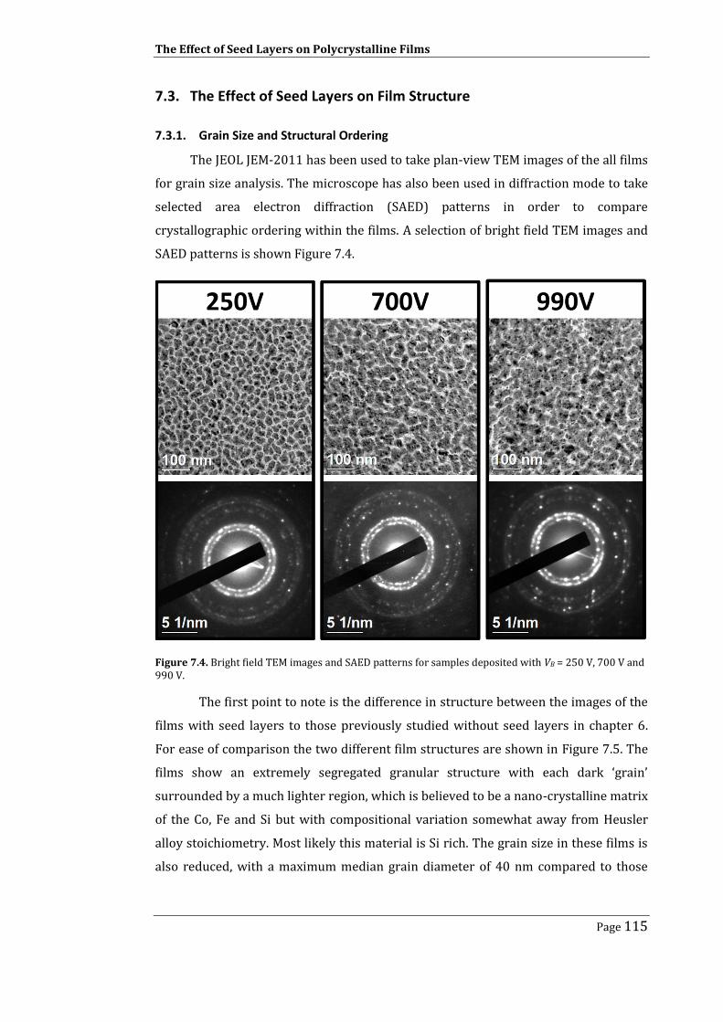
The Effect of Seed Layers on Polycrystalline Films
Page 115
7.3. The Effect of Seed Layers on Film Structure
7.3.1. Grain Size and Structural Ordering
The JEOL JEM-2011 has been used to take plan-view TEM images of the all films
for grain size analysis. The microscope has also been used in diffraction mode to take
selected area electron diffraction (SAED) patterns in order to compare
crystallographic ordering within the films. A selection of bright field TEM images and
SAED patterns is shown Figure 7.4.
Figure 7.4. Bright field TEM images and SAED patterns for samples deposited with VB = 250 V, 700 V and 990 V.
The first point to note is the difference in structure between the images of the
films with seed layers to those previously studied without seed layers in chapter 6.
For ease of comparison the two different film structures are shown in Figure 7.5. The
films show an extremely segregated granular structure with each dark ‘grain’
surrounded by a much lighter region, which is believed to be a nano-crystalline matrix
of the Co, Fe and Si but with compositional variation somewhat away from Heusler
alloy stoichiometry. Most likely this material is Si rich. The grain size in these films is
also reduced, with a maximum median grain diameter of 40 nm compared to those
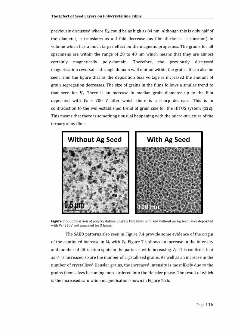
The Effect of Seed Layers on Polycrystalline Films
Page 116
previously discussed where Dm could be as high as 84 nm. Although this is only half of
the diameter, it translates as a 4-fold decrease (as film thickness is constant) in
volume which has a much larger effect on the magnetic properties. The grains for all
specimens are within the range of 28 to 40 nm which means that they are almost
certainly magnetically poly-domain. Therefore, the previously discussed
magnetisation reversal is through domain wall motion within the grains. It can also be
seen from the figure that as the deposition bias voltage is increased the amount of
grain segregation decreases. The size of grains in the films follows a similar trend to
that seen for Hc. There is an increase in median grain diameter up to the film
deposited with VB = 700 V after which there is a sharp decrease. This is in
contradiction to the well-established trend of grain size for the HiTUS system [122].
This means that there is something unusual happening with the micro-structure of the
ternary alloy films.
Figure 7.5. Comparison of polycrystalline Co2FeSi thin films with and without an Ag seed layer deposited with VB=250V and annealed for 3 hours.
The SAED patterns also seen in Figure 7.4 provide some evidence of the origin
of the continued increase in Ms with VB. Figure 7.4 shows an increase in the intensity
and number of diffraction spots in the patterns with increasing VB. This confirms that
as VB is increased so are the number of crystallised grains. As well as an increase in the
number of crystallised Heusler grains, the increased intensity is most likely due to the
grains themselves becoming more ordered into the Heusler phase. The result of which
is the increased saturation magnetisation shown in Figure 7.2b.
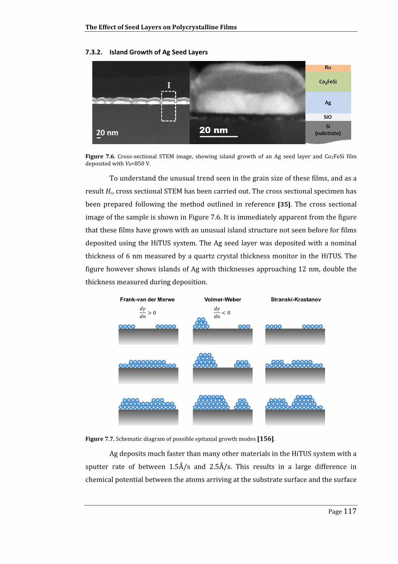
The Effect of Seed Layers on Polycrystalline Films
Page 117
7.3.2. Island Growth of Ag Seed Layers
Figure 7.6. Cross-sectional STEM image, showing island growth of an Ag seed layer and Co2FeSi film deposited with VB=850 V.
To understand the unusual trend seen in the grain size of these films, and as a
result Hc, cross sectional STEM has been carried out. The cross sectional specimen has
been prepared following the method outlined in reference [35]. The cross sectional
image of the sample is shown in Figure 7.6. It is immediately apparent from the figure
that these films have grown with an unusual island structure not seen before for films
deposited using the HiTUS system. The Ag seed layer was deposited with a nominal
thickness of 6 nm measured by a quartz crystal thickness monitor in the HiTUS. The
figure however shows islands of Ag with thicknesses approaching 12 nm, double the
thickness measured during deposition.
Figure 7.7. Schematic diagram of possible epitaxial growth modes [156].
Ag deposits much faster than many other materials in the HiTUS system with a
sputter rate of between 1.5Å/s and 2.5Å/s. This results in a large difference in
chemical potential between the atoms arriving at the substrate surface and the surface
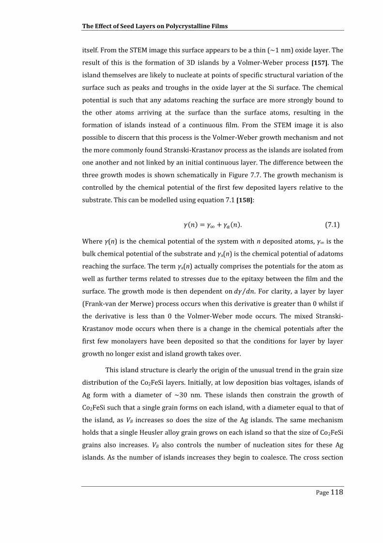
The Effect of Seed Layers on Polycrystalline Films
Page 118
itself. From the STEM image this surface appears to be a thin (~1 nm) oxide layer. The
result of this is the formation of 3D islands by a Volmer-Weber process [157]. The
island themselves are likely to nucleate at points of specific structural variation of the
surface such as peaks and troughs in the oxide layer at the Si surface. The chemical
potential is such that any adatoms reaching the surface are more strongly bound to
the other atoms arriving at the surface than the surface atoms, resulting in the
formation of islands instead of a continuous film. From the STEM image it is also
possible to discern that this process is the Volmer-Weber growth mechanism and not
the more commonly found Stranski-Krastanov process as the islands are isolated from
one another and not linked by an initial continuous layer. The difference between the
three growth modes is shown schematically in Figure 7.7. The growth mechanism is
controlled by the chemical potential of the first few deposited layers relative to the
substrate. This can be modelled using equation 7.1 [158]:
( ) ( )
(7.1)
Where γ(n) is the chemical potential of the system with n deposited atoms, γ∞ is the
bulk chemical potential of the substrate and γa(n) is the chemical potential of adatoms
reaching the surface. The term γa(n) actually comprises the potentials for the atom as
well as further terms related to stresses due to the epitaxy between the film and the
surface. The growth mode is then dependent on ⁄ . For clarity, a layer by layer
(Frank-van der Merwe) process occurs when this derivative is greater than 0 whilst if
the derivative is less than 0 the Volmer-Weber mode occurs. The mixed Stranski-
Krastanov mode occurs when there is a change in the chemical potentials after the
first few monolayers have been deposited so that the conditions for layer by layer
growth no longer exist and island growth takes over.
This island structure is clearly the origin of the unusual trend in the grain size
distribution of the Co2FeSi layers. Initially, at low deposition bias voltages, islands of
Ag form with a diameter of ~30 nm. These islands then constrain the growth of
Co2FeSi such that a single grain forms on each island, with a diameter equal to that of
the island, as VB increases so does the size of the Ag islands. The same mechanism
holds that a single Heusler alloy grain grows on each island so that the size of Co2FeSi
grains also increases. VB also controls the number of nucleation sites for these Ag
islands. As the number of islands increases they begin to coalesce. The cross section

The Effect of Seed Layers on Polycrystalline Films
Page 119
image shown in Figure 7.6 is from the film deposited at 850 V and it shows that a
number of the Ag islands are coalescing to form much larger islands. For the film
deposited with VB =990 V this coalescence has occurred to such an extent that the seed
layer could be considered as being quasi-continuous. The much reduced grain
segregation in Figure 7.4 also shows this. The continuity of the seed layer changes the
growth process of the Co2FeSi, whose structure is now controlled by single grain
nucleation events with limited constraint from the seed layer. This results in much
smaller grains and as a consequence a much reduced energy barrier to magnetisation
reversal. The effect of this is the extremely small coercivity in the films deposited at a
DC bias of 990 V.
7.4. Control of Island Growth with Cr Buffer Layers
To stop the Volmer-Weber process seen in the previous films, a layer of Cr was
deposited to chemically wet the substrate before Ag deposition. Cr deposited using the
HiTUS system is known to grow as a continuous film, even with layer thicknesses of
less than 3 nm, due to its low deposition rate [121]. Cr also has a much better lattice
match with Ag than either crystalline Si or the oxides at the substrate surface, again
reducing any energy contribution from strain and dislocations between the two
layers.
Films have been deposited under the same conditions as those previously
used for the samples with just Ag seed layers. This time however, a 3 nm Cr buffer
layer was deposited before the 6 nm of Ag. The result of this thin layer of Cr is
dramatic. Figure 7.8 shows a bright field TEM image of the specimen in cross section.
From the image it is clear that the Cr buffer layer has prevented the island formation
in the Ag layer producing a film with a peak to peak surface roughness of < 1 nm. All
these films have been grown at a deposition bias voltage of 850 V and the thickness of
the Ag seed layer has been varied between 6 and 30 nm. This was carried out to
observe the effect of Ag thickness. The use of Ag seed layers as a bottom electrode in
STT-MRAM type devices would require a film thickness of greater than 50 nm to
achieve a uniform current density perpendicular to the pillar. It is therefore important
to understand how polycrystalline buffer layers of that thickness influence the
magnetic and structural properties of the Heusler films. The second consideration in
the use of Ag is that it acts as a barrier to Cr diffusion into the Co2FeSi layer, which has
been reported to lead to increased coercivities through structural disorder [159].

The Effect of Seed Layers on Polycrystalline Films
Page 120
Figure 7.8. Bright field TEM image of a film cross section for a Cr (3 nm)/Ag (6 nm) dual seed layer film deposited with VB=850 V.
Magnetically, these specimens are quite different to those deposited with just
an Ag seed layer. The samples were post deposition annealed at 300°C for up to 5
hours under a vacuum of better than 3x10⁻³ Pa. Figure 7.9 shows a typical hysteresis
loop for a Cr buffered film, annealed for 3 hours. It is immediately apparent that the
shape of the hysteresis loop has changed. The squareness of the loop (Mr/Ms) has
increased from 0.61 to 0.85 and the field at which saturation of the magnetisation
occurs has decreased from 1000 Oe to 44 Oe. This means that the magnetisation
reversal mechanism in these films is very different. The coercivity does not change,
which is understandable if thought of in terms of the energy barrier distribution
discussed in section 5.1.3. The energy barrier for the Cr buffered films will show a
substantial peak at the energy corresponding to Hc, whereas those with no Cr buffer
layer will have a much wider and flatter distribution. This accounts for both the low
remanence and increased saturation field. However, the distribution is balanced at the
same point as that for the Cr buffered sample, resulting in similar values for Hc.
The change in behaviour is also symptomatic of a change in the inter-granular
exchange coupling in the films. For the films with only an Ag seed layer the Co2FeSi
grains are almost 100% exchange decoupled. This means that the grains within the
sample must reverse their magnetisation through independent nucleation events. As a
result, this process becomes controlled by the distribution of particle sizes in the film
which in these films is large, with a standard deviation of 0.37. On the other hand, the
films with the Cr buffer layer have a hysteresis loop typical of a film with strong
exchange coupling with high remanent magnetisation, Mr/Ms = 0.88. The reversal is
not entirely exchange controlled as there is not a well-defined nucleation field. This
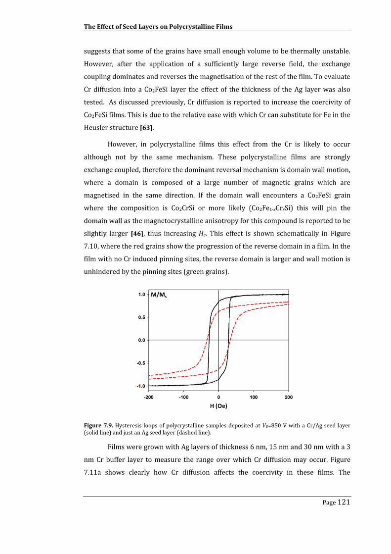
The Effect of Seed Layers on Polycrystalline Films
Page 121
suggests that some of the grains have small enough volume to be thermally unstable.
However, after the application of a sufficiently large reverse field, the exchange
coupling dominates and reverses the magnetisation of the rest of the film. To evaluate
Cr diffusion into a Co2FeSi layer the effect of the thickness of the Ag layer was also
tested. As discussed previously, Cr diffusion is reported to increase the coercivity of
Co2FeSi films. This is due to the relative ease with which Cr can substitute for Fe in the
Heusler structure [63].
However, in polycrystalline films this effect from the Cr is likely to occur
although not by the same mechanism. These polycrystalline films are strongly
exchange coupled, therefore the dominant reversal mechanism is domain wall motion,
where a domain is composed of a large number of magnetic grains which are
magnetised in the same direction. If the domain wall encounters a Co2FeSi grain
where the composition is Co2CrSi or more likely (Co2Fe1-xCrxSi) this will pin the
domain wall as the magnetocrystalline anisotropy for this compound is reported to be
slightly larger [46], thus increasing Hc. This effect is shown schematically in Figure
7.10, where the red grains show the progression of the reverse domain in a film. In the
film with no Cr induced pinning sites, the reverse domain is larger and wall motion is
unhindered by the pinning sites (green grains).
Figure 7.9. Hysteresis loops of polycrystalline samples deposited at VB=850 V with a Cr/Ag seed layer (solid line) and just an Ag seed layer (dashed line).
Films were grown with Ag layers of thickness 6 nm, 15 nm and 30 nm with a 3
nm Cr buffer layer to measure the range over which Cr diffusion may occur. Figure
7.11a shows clearly how Cr diffusion affects the coercivity in these films. The
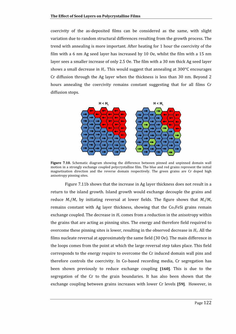
The Effect of Seed Layers on Polycrystalline Films
Page 122
coercivity of the as-deposited films can be considered as the same, with slight
variation due to random structural differences resulting from the growth process. The
trend with annealing is more important. After heating for 1 hour the coercivity of the
film with a 6 nm Ag seed layer has increased by 10 Oe, whilst the film with a 15 nm
layer sees a smaller increase of only 2.5 Oe. The film with a 30 nm thick Ag seed layer
shows a small decrease in Hc. This would suggest that annealing at 300°C encourages
Cr diffusion through the Ag layer when the thickness is less than 30 nm. Beyond 2
hours annealing the coercivity remains constant suggesting that for all films Cr
diffusion stops.
Figure 7.10. Schematic diagram showing the difference between pinned and unpinned domain wall motion in a strongly exchange coupled polycrystalline film. The blue and red grains represent the initial magnetisation direction and the reverse domain respectively. The green grains are Cr doped high anisotropy pinning sites.
Figure 7.11b shows that the increase in Ag layer thickness does not result in a
return to the island growth. Island growth would exchange decouple the grains and
reduce Mr/Ms by initiating reversal at lower fields. The figure shows that Mr/Ms
remains constant with Ag layer thickness, showing that the Co2FeSi grains remain
exchange coupled. The decrease in Hc comes from a reduction in the anisotropy within
the grains that are acting as pinning sites. The energy and therefore field required to
overcome these pinning sites is lower, resulting in the observed decrease in Hc. All the
films nucleate reversal at approximately the same field (30 Oe). The main difference in
the loops comes from the point at which the large reversal step takes place. This field
corresponds to the energy require to overcome the Cr induced domain wall pins and
therefore controls the coercivity. In Co-based recording media, Cr segregation has
been shown previously to reduce exchange coupling [160]. This is due to the
segregation of the Cr to the grain boundaries. It has also been shown that the
exchange coupling between grains increases with lower Cr levels [59]. However, in
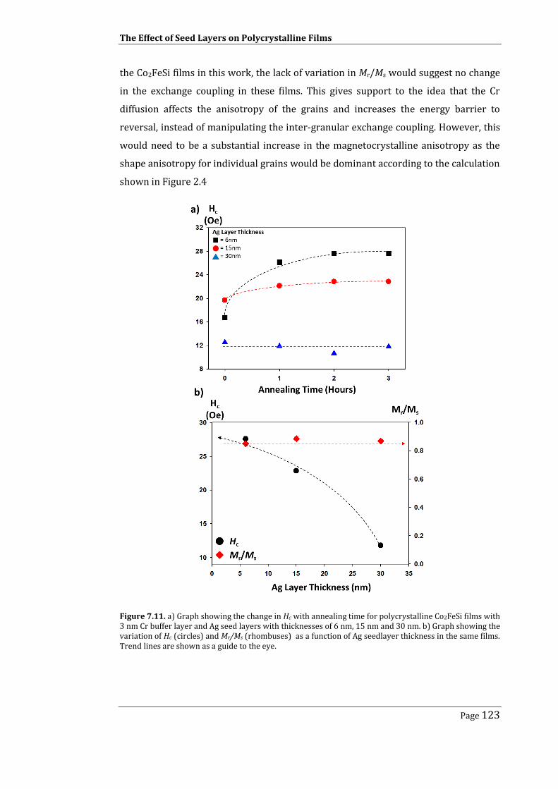
The Effect of Seed Layers on Polycrystalline Films
Page 123
the Co2FeSi films in this work, the lack of variation in Mr/Ms would suggest no change
in the exchange coupling in these films. This gives support to the idea that the Cr
diffusion affects the anisotropy of the grains and increases the energy barrier to
reversal, instead of manipulating the inter-granular exchange coupling. However, this
would need to be a substantial increase in the magnetocrystalline anisotropy as the
shape anisotropy for individual grains would be dominant according to the calculation
shown in Figure 2.4
Figure 7.11. a) Graph showing the change in Hc with annealing time for polycrystalline Co2FeSi films with 3 nm Cr buffer layer and Ag seed layers with thicknesses of 6 nm, 15 nm and 30 nm. b) Graph showing the variation of Hc (circles) and Mr/Ms (rhombuses) as a function of Ag seedlayer thickness in the same films. Trend lines are shown as a guide to the eye.

The Effect of Seed Layers on Polycrystalline Films
Page 124
7.5. Antiferromagnetic Seed Layers
7.5.1. Exchange Bias
By using an antiferromagnetic seed layer the Co2FeSi film can be exchange
biased. Exchange bias is described as the pinning of the magnetisation of a
ferromagnetic (F) layer in one direction due to the effect of an adjacent
antiferromagnetic (AF) layer after field annealing. Initially discovered in 1956 [161],
exchange bias was little more than a curiosity until the discovery of the GMR effect
[12,13], after which it became widely researched due to its technological importance
in spin-valve sensors.
In essence, exchange bias is a product of exchange coupling between the
ferromagnetic and antiferromagnetic layers when the system is field annealed. The AF
layer contributes an extra unidirectional anisotropy field to the F layer, the result of
which is the pinning of the F layer in the direction in which that anisotropy acts. This
is shown schematically in Figure 7.12. Experimentally, this can be achieved by heating
the bilayer through the Néel temperature of the AF layer, then field cooling the stack
back below the ordering temperature. This sets the direction of the AF layer and as a
result the additive anisotropy to the F layer. In practice however it is often unfeasible
to achieve heating through the Néel temperature. In this situation the direction of the
AF layer is set by the thermal activation of a fraction of grains in the film. The
observable effect of this is a shift in the hysteresis loop away from the symmetry
about zero field.
Figure 7.12. Schematic showing the directional pining of ferromagnetic spins at the F/AF interface. The
effect of this pinning on the hysteresis loop of this bilayer is also shown [47].

The Effect of Seed Layers on Polycrystalline Films
Page 125
If polycrystalline Heusler alloys are going to be commercially viable in either
hard drive read heads or STT-MRAM bits then one layer must have the magnetisation
direction pinned. In single crystal films the effective uniaxial anisotropy is enough to
pin one layer once nanoscale features are patterned. For the polycrystalline films this
is not the case. As shown earlier in this chapter these display a 2D random anisotropy.
This must therefore be made uni-directional by exchange biasing.
7.5.2. Film Structure
To induce the maximum exchange bias effect, IrMn with a NiCr seed layer was
deposited before the Co2FeSi. IrMn with a NiCr seed layer has previously been shown
to produce exchange biased films with extremely well controlled parameters
[162,163]. This is because the IrMn is forced to grow with the (111) planes parallel to
the substrate. As it is these (111) planes that couple antiferromagnetically in IrMn,
keeping them within the plane of the film is crucial to providing a large exchange bias.
Figure 7.13. Cross section HRTEM images of exchange biased Co2FeSi thin films with FFTs of Co2FeSi and IrMn grains.

The Effect of Seed Layers on Polycrystalline Films
Page 126
To check this alignment of the IrMn specimens were deposited using the
HiTUS system with a constant VB of 850 V for all layers. The films were then imaged in
cross section using HRTEM. As previously found for the Cr/Ag seed layer the films
have only a small surface roughness (< 1 nm) with an interface roughness of the same
order. From FFTs of the individual layers it was found that both the NiCr and IrMn
layers are strongly textured with their (111) planes in the plane of the film. The
Co2FeSi film however has a distribution of orientations. Growth with the (010) planes
textured into the plane of the substrate appears most commonly. The fast Fourier
FFTs of single grains in the film show the diffraction pattern of the (111) orientation
for IrMn and the diffraction pattern of the (010) planes for Co2FeSi.
To understand the effect of this seed layer on the exchange bias another set of
specimens were grown, with variation of the deposition bias voltage to the NiCr and
IrMn layers. NiCr/IrMn seed layers were deposited with sputter bias voltages of 500 V
and 990 V. This resulted in a median grain diameter of (7.5 ± 0.3) nm for the film
deposited with VB = 500 V and (10.5 ± 0.3) nm with VB = 990 V. These median
diameters were calculated by measuring the lateral diameters of 100 grains in the
cross section images like those in Figure 7.13. This method is not as accurate as using
the Zeiss Particle analyser as was previously used for plan view samples. This method
does have the advantage of being able to measure only the grains in specific layers.
This is of particular interest in these films due to the change of bias voltage for some
layers, whilst the Co2FeSi layer was always deposited with VB = 990 V. This resulted in
a typical grain diameter of 18 nm, however, the statistics could not be performed on
these grains due to their increased size and thus reduced number in the observable
areas of the film cross-section.
7.5.3. Magnetic Measurements
The variation in seed layer grain size has a strong effect on the magnetic properties of
the thin films. All films show the characteristic exchange biased loop shift. However,
the film with the IrMn layer deposited with VB = 990 V shows an exchange bias (Hex)
four times that of the film with the IrMn deposited with VB=500 V. This is shown in
Figure 7.14a.
Figure 7.14b shows how these values of Hex vary as a function of both the IrMn
layer thickness and the temperature at which the film was set. There is a monotonic
increase in Hex with the setting temperature, whilst the variation in Hex with film

The Effect of Seed Layers on Polycrystalline Films
Page 127
thickness is more complex. Hex peaks for an IrMn film thickness of 7 nm and then
gradually decreases. Both the temperature dependence and thickness dependence of
the exchange bias can be explained using the York Model of exchange bias [164]
Figure 7.14. a) Hysteresis loops of thin films with IrMn deposited at VB = 500 V (dashed line) and VB = 990 V (solid line). b) Variation of Hex with IrMn thickness for specimens deposited with VB =990 V.
The York Model of exchange bias describes Hex as being due to the fraction of
antiferromagnetic grains which are ‘set’ in the exchange biasing direction. The fraction
comes from grains whose volumes lie between the limits of the integral in equation
7.2.
∫ ( )
V (7.2)
Vc is the critical volume below which the grains are thermally unstable and Vset is the
volume above which it is impossible to set the grains at a given temperature or field.
The coefficient C* is the interfacial exchange stiffness and contains information about
the exchange coupling between the antiferromagnet and the ferromagnet as well as
the strength of the uniaxial anisotropy induced by the exchange bias. It is assumed
that for these samples C* remains constant and only the grain volume distribution is
affected. The effect of the sputtering bias is shown schematically in Figure 7.15.
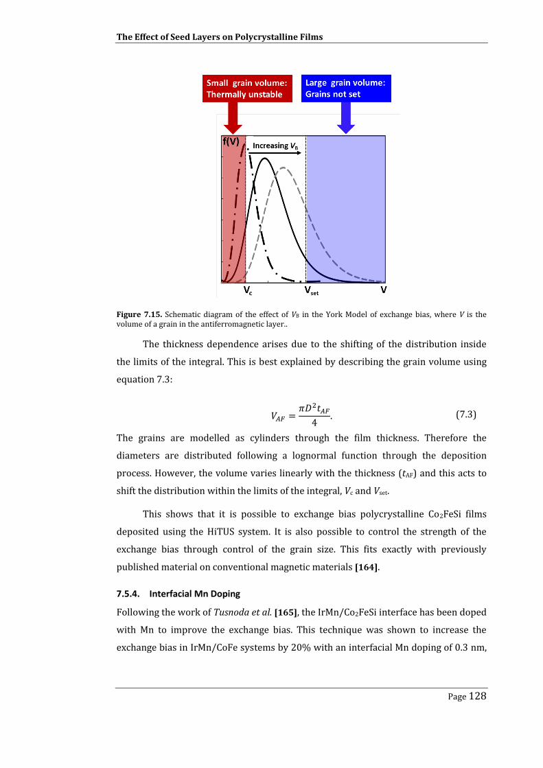
The Effect of Seed Layers on Polycrystalline Films
Page 128
Figure 7.15. Schematic diagram of the effect of VB in the York Model of exchange bias, where V is the volume of a grain in the antiferromagnetic layer..
The thickness dependence arises due to the shifting of the distribution inside
the limits of the integral. This is best explained by describing the grain volume using
equation 7.3:
(7.3)
The grains are modelled as cylinders through the film thickness. Therefore the
diameters are distributed following a lognormal function through the deposition
process. However, the volume varies linearly with the thickness (tAF) and this acts to
shift the distribution within the limits of the integral, Vc and Vset.
This shows that it is possible to exchange bias polycrystalline Co2FeSi films
deposited using the HiTUS system. It is also possible to control the strength of the
exchange bias through control of the grain size. This fits exactly with previously
published material on conventional magnetic materials [164].
7.5.4. Interfacial Mn Doping
Following the work of Tusnoda et al. [165], the IrMn/Co2FeSi interface has been doped
with Mn to improve the exchange bias. This technique was shown to increase the
exchange bias in IrMn/CoFe systems by 20% with an interfacial Mn doping of 0.3 nm,
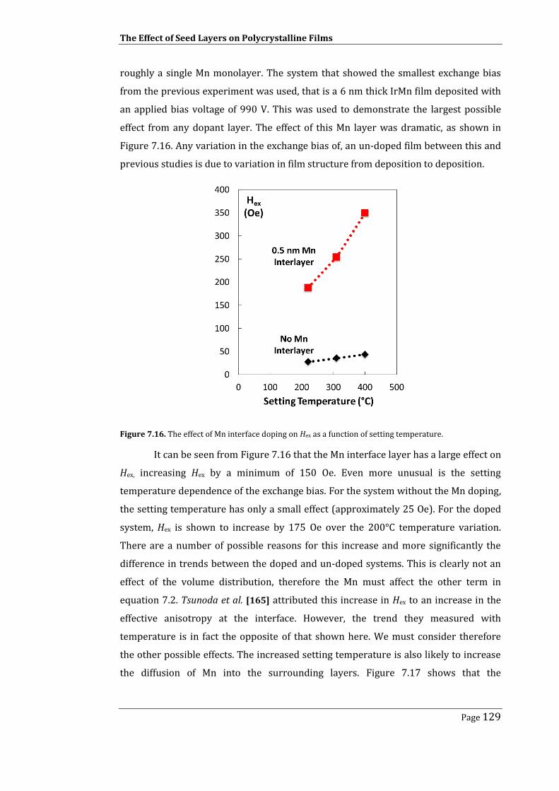
The Effect of Seed Layers on Polycrystalline Films
Page 129
roughly a single Mn monolayer. The system that showed the smallest exchange bias
from the previous experiment was used, that is a 6 nm thick IrMn film deposited with
an applied bias voltage of 990 V. This was used to demonstrate the largest possible
effect from any dopant layer. The effect of this Mn layer was dramatic, as shown in
Figure 7.16. Any variation in the exchange bias of, an un-doped film between this and
previous studies is due to variation in film structure from deposition to deposition.
Figure 7.16. The effect of Mn interface doping on Hex as a function of setting temperature.
It can be seen from Figure 7.16 that the Mn interface layer has a large effect on
Hex, increasing Hex by a minimum of 150 Oe. Even more unusual is the setting
temperature dependence of the exchange bias. For the system without the Mn doping,
the setting temperature has only a small effect (approximately 25 Oe). For the doped
system, Hex is shown to increase by 175 Oe over the 200°C temperature variation.
There are a number of possible reasons for this increase and more significantly the
difference in trends between the doped and un-doped systems. This is clearly not an
effect of the volume distribution, therefore the Mn must affect the other term in
equation 7.2. Tsunoda et al. [165] attributed this increase in Hex to an increase in the
effective anisotropy at the interface. However, the trend they measured with
temperature is in fact the opposite of that shown here. We must consider therefore
the other possible effects. The increased setting temperature is also likely to increase
the diffusion of Mn into the surrounding layers. Figure 7.17 shows that the
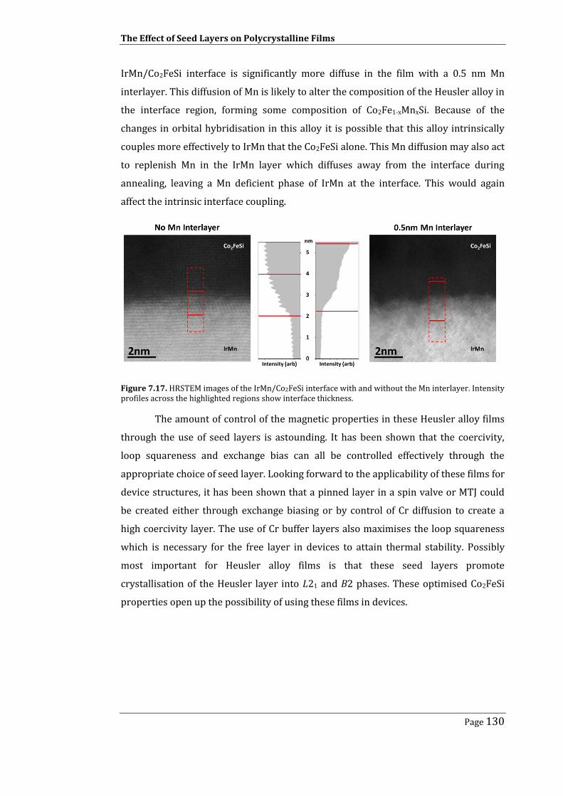
The Effect of Seed Layers on Polycrystalline Films
Page 130
IrMn/Co2FeSi interface is significantly more diffuse in the film with a 0.5 nm Mn
interlayer. This diffusion of Mn is likely to alter the composition of the Heusler alloy in
the interface region, forming some composition of Co2Fe1-xMnxSi. Because of the
changes in orbital hybridisation in this alloy it is possible that this alloy intrinsically
couples more effectively to IrMn that the Co2FeSi alone. This Mn diffusion may also act
to replenish Mn in the IrMn layer which diffuses away from the interface during
annealing, leaving a Mn deficient phase of IrMn at the interface. This would again
affect the intrinsic interface coupling.
Figure 7.17. HRSTEM images of the IrMn/Co2FeSi interface with and without the Mn interlayer. Intensity profiles across the highlighted regions show interface thickness.
The amount of control of the magnetic properties in these Heusler alloy films
through the use of seed layers is astounding. It has been shown that the coercivity,
loop squareness and exchange bias can all be controlled effectively through the
appropriate choice of seed layer. Looking forward to the applicability of these films for
device structures, it has been shown that a pinned layer in a spin valve or MTJ could
be created either through exchange biasing or by control of Cr diffusion to create a
high coercivity layer. The use of Cr buffer layers also maximises the loop squareness
which is necessary for the free layer in devices to attain thermal stability. Possibly
most important for Heusler alloy films is that these seed layers promote
crystallisation of the Heusler layer into L21 and B2 phases. These optimised Co2FeSi
properties open up the possibility of using these films in devices.
Conclusions and Further Work
Page 131
Chapter 8. Conclusions and Further Work
8.1. Conclusions
In this work the magnetic properties of Co-based Heusler alloy compounds have been
correlated with their complex microstructure. Both polycrystalline and epitaxial films
have been grown using HiTUS and magnetron sputtering.
The films deposited using a HiTUS system were found to be polycrystalline
with large grains forming out of an as-deposited amorphous or nano-crystalline
matrix of the atomic components of the alloy after heating. These films have a wide
range of magnetic properties due to the large distribution of structural properties,
primarily grain sizes and phases of ordering. The polycrystalline films have a range of
median diameters from 30 nm to 100 nm. In contrast, the activation volume in these
films shows very little variation, typically giving activation volumes with an equivalent
activation diameter of 40 - 50 nm. As a result, the polycrystalline films change from a
system where magnetisation reversal is controlled by rotation of the magnetisation
through the grain volume to a situation where multiple magnetic domains exist in a
grain, and the magnetisation reversal mechanism is domain wall motion. The
transition between these two regimes results in a number of oddly shaped hysteresis
loops which exhibit two phases of magnetisation reversal.
From SAED and HRTEM it is found that these grains show extremely good
crystalline ordering. However, due to the crystal growth mechanisms, the large grains
in these films result from the coalescence of two or more grains. This results in
regions of structural disorder in the grains which act as domain wall pins. The effect of
this is seen in the hysteresis loops of the films with an increased fraction of larger
grains, where the increased coercivity is the result of pinned domain wall motion. The
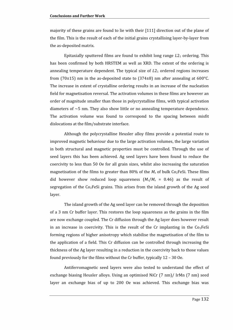
Conclusions and Further Work
Page 132
majority of these grains are found to lie with their [111] direction out of the plane of
the film. This is the result of each of the initial grains crystallising layer-by-layer from
the as-deposited matrix.
Epitaxially sputtered films are found to exhibit long range L21 ordering. This
has been confirmed by both HRSTEM as well as XRD. The extent of the ordering is
annealing temperature dependent. The typical size of L21 ordered regions increases
from (70±15) nm in the as-deposited state to (374±8) nm after annealing at 600°C.
The increase in extent of crystalline ordering results in an increase of the nucleation
field for magnetisation reversal. The activation volumes in these films are however an
order of magnitude smaller than those in polycrystalline films, with typical activation
diameters of ~5 nm. They also show little or no annealing temperature dependence.
The activation volume was found to correspond to the spacing between misfit
dislocations at the film/substrate interface.
Although the polycrystalline Heusler alloy films provide a potential route to
improved magnetic behaviour due to the large activation volumes, the large variation
in both structural and magnetic properties must be controlled. Through the use of
seed layers this has been achieved. Ag seed layers have been found to reduce the
coercivity to less than 50 Oe for all grain sizes, whilst also increasing the saturation
magnetisation of the films to greater than 80% of the Ms of bulk Co2FeSi. These films
did however show reduced loop squareness (Mr/Ms = 0.46) as the result of
segregation of the Co2FeSi grains. This arises from the island growth of the Ag seed
layer.
The island growth of the Ag seed layer can be removed through the deposition
of a 3 nm Cr buffer layer. This restores the loop squareness as the grains in the film
are now exchange coupled. The Cr diffusion through the Ag layer does however result
in an increase in coercivity. This is the result of the Cr implanting in the Co2FeSi
forming regions of higher anisotropy which stabilise the magnetisation of the film to
the application of a field. This Cr diffusion can be controlled through increasing the
thickness of the Ag layer resulting in a reduction in the coercivity back to those values
found previously for the films without the Cr buffer, typically 12 – 30 Oe.
Antiferromagnetic seed layers were also tested to understand the effect of
exchange biasing Heusler alloys. Using an optimised NiCr (7 nm)/ IrMn (7 nm) seed
layer an exchange bias of up to 200 Oe was achieved. This exchange bias was

Conclusions and Further Work
Page 133
improved through the use of Mn interfacial doping. By inserting a 0.5 nm Mn layer at
the IrMn/Co2FeSi interface the exchange bias was increased to 375 Oe. From cross
sectional STEM it was found that this Mn layer increases the interface roughness,
showing diffusive contrast out to 10 monolayers, whereas the film without the Mn
interlayer only showed this diffusion up to 4 monolayers. Although this roughness
may affect the exchange bias, it is more likely that this inter-diffusion changes the
atomic composition at the interface, thus increasing the AF/F exchange coupling and
as a result the exchange bias.
Through the use of seed layers it was possible to tailor both the structure and
magnetic properties of polycrystalline Heusler alloys. It was possible to achieve values
of saturation magnetisation up to 90% of that of bulk Co2FeSi. The ordered grains in
these films also appear to be L21 or B2 ordered from SAED and HRTEM. However, the
degree of spin polarisation achievable from these films remains uncertain as devices
through which this could be measured have not been fabricated.
8.2. Future Work
8.2.1. Observation of Domain Structures
In order to truly understand the reversal mechanisms in both the single
crystal and polycrystalline films the domain mechanisms must be observed directly.
There are a number of techniques that allow this, principally Kerr effect microscopy,
magnetic force microscopy (MFM) and Lorentz TEM. Each of these techniques has
their own distinct advantages and disadvantages. However, a combination of these
techniques would give a more complete picture of the complex magnetisation reversal
processes in these films. Kerr microscopy has previously been carried out on single
crystal films of the similar alloy Co2CrFeAl [67]. By taking images at different points
along the hysteresis loop it was possible to image the progress of domain wall motion.
However, this was not a dynamic measurement and the resolution is limited such that
the Barkhausen jumps that define the activation volume may be below both the optical
and time resolution limit. Kerr microscopy may however be able to shed some light on
the origin of the uniaxial anisotropy in the single crystal films measured in this work,
as was previously demonstrated in [67].
To achieve the resolution necessary to image the 5 nm activation diameters
Lorentz TEM must be considered. MFM has not been widely used in Heusler systems,

Conclusions and Further Work
Page 134
but demonstrations in other systems would suggest that this technique could be
applicable to the thin films in this work. MFM has been demonstrated at a resolution
of below 30 nm, making it potentially able to image the domain structure of single
grains in the polycrystalline films in this work. Unfortunately, it is not usually possible
to apply large fields in conventional MFM systems, which may make certain parts of
the hysteresis loops difficult to access.
Lorentz TEM may provide the best possible technique for the direct
observation of magnetisation reversal processes due to its high resolution (<10 nm).
This has been demonstrated in a number of systems, though recently it has primarily
been used to observe domain processes in nanowires for racetrack memory [166].
New advances in microscope technology may also allow nanometre resolution for
Lorentz TEM, although as yet nothing has been published on these systems. For the
polycrystalline films, this technique should be immediately applicable due to the
previously demonstrated grain growth in these films when deposited onto TEM grids.
For single crystal films, this technique is potentially much more difficult because the
films must be thinned. This will change the magnetic properties of the films
dramatically. This would make it difficult to correlate the Lorentz TEM results with
the magnetic measurements.
8.2.2. Device Fabrication
The next step in this work would be the fabrication of nano-pillar GMR devices
to perform measurements of magnetoresistance, as well as to demonstrate spin
transfer torque induced switching in these materials. Recently, fabrication of pseudo-
spin valves has been reported in polycrystalline Heusler alloy systems. These systems
demonstrated CPP-GMR in both Co2Fe(Al0.5,Si0.5) and Co2Fe(Ga0.5Ge0.5) based devices
[44]. Relatively high GMR values of up to 10% at room temperature were reported.
The devices also had low resistance when compared to previous Heusler alloy based
devices [44]. The other important step in this study was the use of low annealing
temperatures, typically 235°C but with a maximum of 350°C. This demonstrated the
feasibility of the use polycrystalline Heusler alloys for commercial applications such as
hard disk drive read heads. Although exceptionally high TMR values were previously
demonstrated using single crystal films these required much higher annealing
temperatures of above 500°C [34].
Conclusions and Further Work
Page 135
Figure 8.1. TEM image of a potential device film.
As a step towards creating a device, films have been deposited using the
HiTUS system with structures similar to those used in these devices. Cross-section
TEM images of these films are shown in Figure 8.1. The figure shows that these films
are approaching the required properties for device structures. The interfaces in the
film have low roughness, <1 nm, whilst also demonstrating single step magnetisation
reversal. Figure 8.1 also shows that the 2.5 nm thick free layer remains continuous
over the entire area imaged. After imaging a number of areas it was found that this
layer was continuous across the entire film. These films have yet to be patterned into
devices and their electronic properties measured.

List of Symbols
Page 136
List of Symbols
a Lattice constant for cubic material ao Atomic radius Aex Exchange stiffness coefficient A(u) Aperture term in the contrast transfer function B(u) Aberration term in the contrast transfer function β Full width half maxima of diffraction peak Cs Spherical aberration coefficient γ(n) Chemical potential of a system with n atoms γ∞ Chemical potential of a substrate γa Chemical potential of an adatom γgm Gyromagnetic ratio χirr Irreversible susceptibility dhkl Reciprocal space atomic plane spacing Dact Magnetic activation diameter Dm Median grain diameter DXRD Crystallite size from X-ray diffraction δ Domain wall width Eact Bonding activation energy EF Fermi Energy Eex Exchange energy EK Anisotropy energy Ems Magnetostatic energy E(u) Envelope term in the contrast transfer function ΔE Energy barrier to reversal 𝜂(u) Exponent solution to the contrast transfer function f0 Attempt frequency Δf Defocus value Fi Force exerted in direction i g Laue vector for reciprocal space atomic plane
gB Laue vector for reciprocal space atomic plane meeting the Bragg condition
h,k,l Miller indices Hc Coercive Field Hex Exchange bias field Hf Fluctuation field Hi External magnetic field in direction i HK Anisotropy field Hn Reverse domain nucleation field Jex Exchange integral K0,1,2 Magnetocrystalline anisotropy constants Ks Shape anisotropy constant
L Laue vector describing difference between incident and exit radiation
LB Laue vector for radiation meeting the Bragg condition M Magnetisation Mr Remanent magnetisation Ms Saturation magnetisation m* Effective electron mass

List of Abbreviations
Page 137
Nd Shape demagnetising factor Nv Number of valence electrons Nf.u. Number of valence electrons per formula unit λe Electron wavelength λX X-ray wavelength Φ Magnetic flux P1 (2) Spin polarisation of device electrode 1 (2) ρ↑(↓) Resistivity of spin up (down) charge carriers ρP(T) Thermal resistivity ρ↑↓ Thermal spin scattering resistivity ra Atomic separation rd Radius of an electron d orbital Si(j) Spin angular momentum of atom i (j) S1(H) 1st Order magnetic viscosity coefficient S2(H) 2nd Order magnetic viscosity coefficient s↑(↓) Fraction of electrons with spin up (down) σlnD Standard deviation of ln(D) T(u) Contrast transfer function (CTF) tA Annealing time Τ Magnetisation relaxation time τSTT Spin transfer toque θB Bragg angle Θ Debye temperature U Spatial frequency μi Magnetic moment in direction i νres Resonant frequency vcg Crystal growth velocity vo Atomic jump frequency Vact Magnetic activation volume VB HiTUS sputtering bias voltage
Mean of ln(D)
List of Abbreviations
AGFM Alternating gradient force magnetometer AMR Anisotropic magnetoresistance CIP Current-in-plane CMOS Complementary metal-oxide-semiconductor CPP Current-perpendicular-to-plane DCD DC demagnetised DRAM Dynamic random access memory EDX Electron dispersive X-ray spectroscopy fcc Face centred cubic FFT Fast Fourier transform FWHM Full width half maximum GMR Giant magnetoresistance hcp Hexagonal close packed HiTUS High target utilisation sputtering
Page 138
HMF Half metallic ferromagnet (HR)STEM (High resolution) Scanning transmission electron microscopy (HR)TEM (High resolution) Transmission electron microscopy IRM Isothermal remanence MOSFET Metal-oxide-semiconductor field effect transistor MRAM Magnetic random access memory MTJ Magnetic tunnel junction RKKY Ruderman Kittel Kasuya Yoshida Spin-FET Spin field effect transistor STT Spin transfer torque TMR Tunnelling magnetoresistance VSM Vibrating sample magnetometer WBDF Weak-beam dark-field XRD X-ray diffraction

References
Page 139
References
1 Sze, S. M. & Ng, K. K. Physics of Semiconductor Devices. Wiley, (2006). 2 Moore, G. E. Proceedings of the IEEE 86, 82-85, (1998). 3 Rizzo, B. D. NVIDIA Introduces GeForce GTX TITAN: DNA Of The World's Fastest
Supercomputer, Powered By World's Fastest GPU, <http://nvidianews.nvidia.com/Releases/NVIDIA-Introduces-GeForce-GTX-TITAN-DNA-of-the-World-s-Fastest-Supercomputer-Powered-by-World-s-Fa-925.aspx> (2013).
4 Kim, N. S., Austin, T., Baauw, D., Mudge, T., Flautner, K., Hu, J. S., Irwin, M. J., Kandemir, M. & Narayanan, V. Computer 36, 68-75, (2003).
5 Awschalom, D. D. & Flatte, M. E. Nature Physics 3, 153-159, (2007). 6 Prinz, G. A. Science 282, 1660-1663, (1998). 7 Prinz, G. A. Journal of Magnetism and Magnetic Materials 200, 57-68, (1999). 8 Datta, S. & Das, B. Applied Physics Letters 56, 665-667, (1990). 9 Thomson, W. Proceedings of the Royal Society of London 8, 546-550, (1856). 10 Brataas, A., Kent, A. D. & Ohno, H. Nature Materials 11, 372-381, (2012). 11 Parkin, S. S. P. Physical Review Letters 67, 3598-3601, (1991). 12 Binasch, G., Grünberg, P., Saurenbach, F. & Zinn, W. Physical Review B 39, 4828-
4830, (1989). 13 Baibich, M. N., Broto, J. M., Fert, A., Van Dau, F. N., Petroff, F., Etienne, P.,
Creuzet, G., Friederich, A. & Chazelas, J. Physical Review Letters 61, 2472-2475, (1988).
14 Mott, N. F. Proceedings of the Royal Society of London. Series A, Mathematical and Physical Sciences 153, 699-717, (1936).
15 Mott, N. F. Proceedings of the Royal Society of London. Series A, Mathematical and Physical Sciences 156, 368-382, (1936).
16 Campbell, I. A., Fert, A. & Pomeroy, R. Philosophical Magazine 15, 977-983, (1967).
17 Fert, A. & Campbell, I. A. Physical Review Letters 21, 1190-1192, (1968). 18 Thompson, S. M. Journal of Physics D: Applied Physics 41, 093001, (2008). 19 Nakatani, T. M., Furubayashi, T. & Hono, K. Journal of Applied Physics 109,
07B724-723, (2011). 20 Julliere, M. Physics Letters A 54, 225-226, (1975). 21 Miyazaki, T. & Tezuka, N. Journal of Magnetism and Magnetic Materials 139, 231-
234, (1995). 22 Moodera, J. S., Kinder, L. R., Wong, T. M. & Meservey, R. Physical Review Letters
74, 3273-3276, (1995). 23 Butler, W. H., Zhang, X. G., Schulthess, T. C. & MacLaren, J. M. Physical Review B
63, 054416, (2001). 24 Ikeda, S., Hayakawa, J., Ashizawa, Y., Lee, Y. M., Miura, K., Hasegawa, H., Tsunoda,
M., Matsukura, F. & Ohno, H. Applied Physics Letters 93, 082508-082503, (2008). 25 Slonczewski, J. C. Journal of Magnetism and Magnetic Materials 159, 1-7, (1996). 26 Berger, L. Journal of Applied Physics 55, 1954-1956, (1984). 27 Maekawa, S., Valenzuela, S. O., Saitoh, E. & Kimura, T. Spin Current. OUP Oxford,
(2012). 28 de Groot, R. A., Mueller, F. M., Engen, P. G. v. & Buschow, K. H. J. Physical Review
Letters 50, 2024-2027, (1983). 29 Felser, C. & Hilllebrands, B. Journal of Physics D: Applied Physics 40, (2007).

References
Page 140
30 Kandpal, H. C., Fecher, G. H. & Felser, C. Journal of Physics D: Applied Physics 40, 1507, (2007).
31 Blum, C. G. F., Jenkins, C. A., Barth, J., Felser, C., Wurmehl, S., Friemel, G., Hess, C., Behr, G., Buchner, B., Reller, A., Riegg, S., Ebbinghaus, S. G., Ellis, T., Jacobs, P. J., Kohlhepp, J. T. & Swagten, H. J. M. Applied Physics Letters 95, 161903-161903, (2009).
32 Keizer, R. S., Goennenwein, S. T. B., Klapwijk, T. M., Miao, G., Xiao, G. & Gupta, A. Nature 439, 825-827, (2006).
33 Son, Y.-W., Cohen, M. L. & Louie, S. G. Nature 444, 347-349, (2006). 34 Tezuka, N., Ikeda, N., Mitsuhashi, F. & Sugimoto, S. Applied Physics Letters 94,
162504-162503, (2009). 35 Lazarov, V. K., Yoshida, K., Sato, J., Hasnip, P. J., Oogane, M., Hirohata, A. & Ando,
Y. Applied Physics Letters 98, 242508-242503, (2011). 36 Ambrose, T., Krebs, J. J. & Prinz, G. A. Applied Physics Letters 76, 3280-3282,
(2000). 37 Ebke, D., Schmalhorst, J., Liu, N. N., Thomas, A., Reiss, G. & Hutten, A. Applied
Physics Letters 89, 162506-162503, (2006). 38 Inomata, K., Okamura, S., Miyazaki, A., Kikuchi, M., Tezuka, N., Wojcik, M. &
Jedryka, E. Journal of Physics D: Applied Physics 39, 816, (2006). 39 Nakatani, T. M., Rajanikanth, A., Gercsi, Z., Takahashi, Y. K., Inomata, K. & Hono, K.
Journal of Applied Physics 102, 033916-033918, (2007). 40 Shan, R., Sukegawa, H., Wang, W. H., Kodzuka, M., Furubayashi, T., Ohkubo, T.,
Mitani, S., Inomata, K. & Hono, K. Physical Review Letters 102, 246601, (2009). 41 Nakatani, T. M., Furubayashi, T., Kasai, S., Sukegawa, H., Takahashi, Y. K., Mitani, S.
& Hono, K. Applied Physics Letters 96, 212501-212503, (2010). 42 Sukegawa, H., Kasai, S., Furubayashi, T., Mitani, S. & Inomata, K. Applied Physics
Letters 96, 042508-042503, (2010). 43 Furubayashi, T., Kodama, K., Goripati, H. S., Takahashi, Y. K., Inomata, K. & Hono,
K. Journal of Applied Physics 105, 07C305-303, (2009). 44 Nakatani, T. M., Du, Y., Takahashi, Y. K., Furubayashi, T. & Hono, K. Acta
Materialia 61, 3695-3702, (2013). 45 Good, P. I. & Hardin, J. W. Common Errors in Statistics (and How to Avoid Them).
Wiley, (2009). 46 Trudel, S., Gaier, O., Hamrle, J. & Hillebrands, B. Journal of Physics D: Applied
Physics 43, 193001, (2010). 47 Cullity, B. D. & Graham, C. D. Introduction to Magnetic Materials. Wiley, (2009). 48 Heisenberg, W. Z. Physik 38, 411-426, (1926). 49 O'Handley, R. C. Modern Magnetic Materials: Principles and Applications. Wiley,
(1999). 50 Morrish, A. H. & Society, I. M. The Physical Principles of Magnetism. Wiley, (1965). 51 Ruderman, M. A. & Kittel, C. Physical Review 96, 99-102, (1954). 52 Kasuya, T. Prog. Theor. Phys. 16, 45-57, (1956). 53 Yosida, K. Physical Review 106, 893-898, (1957). 54 Campbell, I. A. Journal of Physics F: Metal Physics 2, L47, (1972). 55 Parkin, S. S. P., More, N. & Roche, K. P. Physical Review Letters 64, 2304-2307,
(1990). 56 Ashcroft, N. & Mermin, D. Solid State Physics. Thomson Learning, (1976). 57 Crangle, J. Solid-State Magnetism. Van Nostrand Reinhold, (1991).
References
Page 141
58 Parkin, S. S. P., Bhadra, R. & Roche, K. P. Physical Review Letters 66, 2152-2155, (1991).
59 O'Grady, K., Chantrell, R. & Sanders, I. IEEE Transactions on Magnetics 29, 286-291, (1993).
60 Hirohata, A. & Otani, Y. in Epitaxial Ferromagnetic Films and Spintronic Applications (eds A. Hirohata & Y Otani) Ch. 9, 207-235 Research Signpost, (2009).
61 Trudel, S., Wolf, G., Hamrle, J., Hillebrands, B., Klaer, P., Kallmayer, M., Elmers, H.-J., Sukegawa, H., Wang, W. & Inomata, K. Physical Review B 83, 104412, (2011).
62 Hashimoto, M., Herfort, J., Schonherr, H. P. & Ploog, K. H. Applied Physics Letters 87, 102506-102503, (2005).
63 Hirohata, A., Kurebayashi, H., Okamura, S., Tezuka, N. & Inomata, K. IEEE Transactions on Magnetics 41, 2802-2804, (2005).
64 Moosbuhler, R., Bensch, F., Dumm, M. & Bayreuther, G. Journal of Applied Physics 91, 8757-8759, (2002).
65 Stoner, E. C. & Wohlfarth, E. P. Philosophical Transactions of the Royal Society. Section A 240, 599-642, (1948).
66 Jiles, D. Introduction to magnetism and magnetic materials, 2nd ed. Chapman and Hall, (1998).
67 Hamrle, J., Blomeier, S., Gaier, O., Hillebrands, B., Schafer, R. & Jourdan, M. Journal of Applied Physics 100, 103904-103904, (2006).
68 Néel, L. Ann. Geophys. 5, (1949). 69 Suh, H.-J., Heo, C., You, C.-Y., Kim, W., Lee, T.-D. & Lee, K.-J. Physical Review B 78,
064430, (2008). 70 Street, R. & Woolley, J. C. Proceedings of the Physical Society. Section A 62, 562-
572, (1949). 71 Gaunt, P. Journal of Applied Physics 59, 4129-4132, (1986). 72 Néel, L. J. Phys. Radium 12, 339-351, (1951). 73 Wohlfarth, E. P. Journal of Physics F: Metal Physics 14, 155, (1984). 74 Street, R., Woolley, J. C. & Smith, P. B. Proceedings of the Physical Society. Section
B 65, 679, (1952). 75 El-Hilo, M., O’Grady, K. & Chantrell, R. W. Journal of Magnetism and Magnetic
Materials 248, 360-373, (2002). 76 Mee, C. D. & Daniel, E. D. Magnetic recording technology. McGraw-Hill, (1996). 77 Dutson, J. D., O'Grady, K., Bin, L., Kubota, Y. & Platt, C. L. IEEE Transactions on
Magnetics 39, 2344-2346, (2003). 78 Nishino, Y., Kato, M., Asano, S., Soda, K., Hayasaki, M. & Mizutani, U. Physical
Review Letters 79, 1909-1912, (1997). 79 Wernick, J. H., Hull, G. W., Geballe, T. H., Bernardini, J. E. & Waszczak, J. V.
Materials Letters 2, 90-92, (1983). 80 König, M., Wiedmann, S., Brüne, C., Roth, A., Buhmann, H., Molenkamp, L. W., Qi,
X.-L. & Zhang, S.-C. Science 318, 766-770, (2007). 81 Heusler, F. S., W.; Haupt, E. . Verhandlungen der Deutschen Physikalischen
Gesellschaft 5, 219-223, (1903). 82 Sukegawa, H., Wang, W., Shan, R., Nakatani, T., Inomata, K. & Hono, K. Physical
Review B 79, 184418, (2009). 83 Block, T., Felser, C., Jakob, G., Ensling, J., Mühling, B., Gütlich, P. & Cava, R. J.
Journal of Solid State Chemistry 176, 646-651, (2003).
References
Page 142
84 Graf, T., Felser, C. & Parkin, S. S. P. Prog Solid St Chem 39, 50-50, (2011). 85 Yamada, S., Sagar, J., Honda, S., Lari, L., Takemoto, G., Itoh, H., Hirohata, A., Mibu,
K., Miyao, M. & Hamaya, K. Physical Review B 86, 174406, (2012). 86 Galanakis, I., Dederichs, P. H. & Papanikolaou, N. Physical Review B 66, 174429,
(2002). 87 Fujii, S. I., Shoji, A. S. Journal of the Physical Society of Japan 64, 6, (1995). 88 Meinert, M., Schmalhorst, J.-M., Glas, M., Reiss, G., Arenholz, E., Böhnert, T. &
Nielsch, K. Physical Review B 86, 054420, (2012). 89 Kandpal, H. C., Fecher, G. H., Felser, C. & Schönhense, G. Physical Review B 73,
094422, (2006). 90 Wurmehl, S., Fecher, G. H., Kandpal, H. C., Ksenofontov, V., Felser, C., Lin, H.-J. &
Morais, J. Physical Review B 72, 184434, (2005). 91 Gercsi, Z. & Hono, K. Journal of Physics: Condensed Matter 19, 326216, (2007). 92 Chadov, S., Fecher, G. H., Felser, C., Minar, J., Braun, J. & Ebert, H. Journal of
Physics D: Applied Physics 42, 084002, (2009). 93 Kohn, W. Reviews of Modern Physics 71, 1253-1266, (1999). 94 Vladimir, I. A., Aryasetiawan, F. & Lichtenstein, A. I. Journal of Physics: Condensed
Matter 9, 767, (1997). 95 Slater, J. C. Physical Review 49, 537-545, (1936). 96 Pauling, L. Physical Review 54, 899-904, (1938). 97 Kübler, J. Theory of Itinerant Electron Magnetism. OUP Oxford, (2000). 98 Balke, B., Fecher, G. H. & Felser, C. Applied Physics Letters 90, 242503-242503,
(2007). 99 Kubota, T., Tsunegi, S., Oogane, M., Mizukami, S., Miyazaki, T., Naganuma, H. &
Ando, Y. Applied Physics Letters 94, 122504-122503, (2009). 100 Li, G.-N., Jin, Y.-J. & Lee Jae, I. Chinese Physics B 19, 097102, (2010). 101 Takamura, Y., Nakane, R., Munekata, H. & Sugahara, S. Journal of Applied Physics
103, 07D719-713, (2008). 102 Oogane, M., Shinano, M., Sakuraba, Y. & Ando, Y. Journal of Applied Physics 105,
907C903-903, (2009). 103 Schneider, H., Jakob, G., Kallmayer, M., Elmers, H. J., Cinchetti, M., Balke, B.,
Wurmehl, S., Felser, C., Aeschlimann, M. & Adrian, H. Physical Review B 74, 174426, (2006).
104 Sagar, J., Sukegawa, H., Lari, L., Lazarov, V. K., Mitani, S., O'Grady, K. & Hirohata, A. Applied Physics Letters 101, 102410-102414, (2012).
105 Ksenofontov, V., Wojcik, M., Wurmehl, S., Schneider, H., Balke, B., Jakob, G. & Felser, C. Journal of Applied Physics 107, 09B106-103, (2010).
106 Yang, F. J., Wei, C. & Chen, X. Q. Applied Physics Letters 102, 172403-172404, (2013).
107 Niculescu, V., Budnick, J. I., Hines, W. A., Raj, K., Pickart, S. & Skalski, S. Physical Review B 19, 452-464, (1979).
108 Miura, Y., Nagao, K. & Shirai, M. Physical Review B 69, 144413, (2004). 109 Bruski, P., Erwin, S. C., Ramsteiner, M., Brandt, O., Friedland, K. J., Farshchi, R.,
Herfort, J. & Riechert, H. Physical Review B 83, 140409, (2011). 110 Nagao, K., Miura, Y. & Shirai, M. Physical Review B 73, 104447, (2006). 111 Kazutaka, A., Yoshio, M., Yasunori, S. & Masafumi, S. Journal of Physics:
Condensed Matter 21, 064244, (2009).

References
Page 143
112 Yoshio, M., Hirohisa, U., Yoshihiro, O., Kazutaka, N. & Masafumi, S. Journal of Physics: Condensed Matter 19, 365228, (2007).
113 Saito, T., Katayama, T., Ishikawa, T., Yamamoto, M., Asakura, D., Koide, T., Miura, Y. & Shirai, M. Physical Review B 81, 144417, (2010).
114 Hashemifar, S. J., Kratzer, P. & Scheffler, M. Physical Review Letters 94, 096402, (2005).
115 Shirai, M., ; Miura, Yoshio,; Abe, Kazutaka. in Epitaxial Ferromagnetic Films and Spintronic Applications (ed Atsufumi.; Otani Hirohata, Yoshichika) Ch. 8, 187-205 Research Signpost, (2009).
116 Sakuraba, Y., Hattori, M., Oogane, M., Ando, Y., Kato, H., Sakuma, A., Miyazaki, T. & Kubota, H. Applied Physics Letters 88, 192508-192503, (2006).
117 Yuasa, S., Nagahama, T., Fukushima, A., Suzuki, Y. & Ando, K. Nature Materials 3, 868-871, (2004).
118 Mavropoulos, P., Ležaić, M. & Blügel, S. Physical Review B 72, 174428, (2005). 119 Tsunegi, S., Sakuraba, Y., Oogane, M., Takanashi, K. & Ando, Y. Applied Physics
Letters 93, 112506-112503, (2008). 120 Wang, W., Sukegawa, H., Shan, R., Furubayashi, T. & Inomata, K. Applied Physics
Letters 92, 221912-221913, (2008). 121 Vopsaroiu, M., Fernandez, G. V., Thwaites, M. J., Anguita, J., Grundy, P. J. & Grady,
K. O. Journal of Physics D: Applied Physics 38, 490, (2005). 122 Vopsaroiu, M., Thwaites, M. J., Rand, S., Grundy, P. J. & O'Grady, K. IEEE
Transactions on Magnetics 40, 2443-2445, (2004). 123 Hirohata, A., Ladak, S., Aley, N. P. & Hix, G. B. Applied Physics Letters 95, 252506-
252506-252503, (2009). 124 Fleet, L. R., Cheglakov, G., Yoshida, K., Lazarov, V. K., Nakayama, T. & Hirohata, A.
Journal of Physics D: Applied Physics 45, 032001, (2012). 125 Stuart, R. V. Vacuum Technology, Thin Films, and Spluttering: An Introduction.
Academic, (1983). 126 Geiersbach, U., Bergmann, A. & Westerholt, K. Journal of Magnetism and
Magnetic Materials 240, 546-549, (2002). 127 Williams, D. B. & Carter, C. B. Transmission Electron Microscopy: A Textbook for
Materials Science. Spectrometry. Plenum Press, (1996). 128 Rose, H. Optik 85, 19-24, (1990). 129 Wall, J., Langmore, J., Isaacson, M. & Crewe, A. V. Proceedings of the National
Academy of Sciences 71, 1-5, (1974). 130 Cullity, B. D. & Stock, S. R. Elements of X-Ray Diffraction (3rd Edition). Prentice
Hall, (2001). 131 Flanders, P. J. Journal of Applied Physics 63, 3940-3945, (1988). 132 O'Grady, K., Lewis, V. G. & Dickson, D. P. E. Journal of Applied Physics 73, 5608-
5613, (1993). 133 Richter, H. J., Hempel, K. A. & Pfeiffer, J. Review of Scientific Instruments 59, 1388-
1393, (1988). 134 Zijlstra, H. Review of Scientific Instruments 41, 1241-1243, (1970). 135 Roos, W., Hempel, K. A., Voigt, C., Dederichs, H. & Schippan, R. Review of
Scientific Instruments 51, 612-613, (1980). 136 Chantrell, R. W. & Grady, K. O. Journal of Physics D: Applied Physics 25, 1, (1992). 137 van de Veerdonk, R. J. M., Xiaowei, W. & Weller, D. IEEE Transactions on
Magnetics 38, 2450-2452, (2002).

References
Page 144
138 El-Hilo, M., O'Grady, K. & Chantrell, R. W. Journal of Magnetism and Magnetic Materials 109, L164-L168, (1992).
139 Foner, S. Review of Scientific Instruments 27, 548-548, (1956). 140 Mallinson, J. Journal of Applied Physics 37, 2514-2515, (1966). 141 Lu, K., Wang, J. T. & Wei, W. D. Journal of Applied Physics 69, 522-524, (1991). 142 Scott, M. & Luborsky, F. Butter-Worths Co. Ltd, London, 151, (1983). 143 Lu, K. & Wang, J. T. Journal of Crystal Growth 94, 448-454, (1989). 144 O'Grady, K. & Bradbury, A. Journal of Magnetism and Magnetic Materials 39, 91-
94, (1983). 145 Hirohata, A., Kikuchi, M., Tezuka, N., Inomata, K., Claydon, J. S., Xu, Y. B. & van der
Laan, G. Current Opinion in Solid State and Materials Science 10, 93-107, (2006). 146 Hÿtch, M. J., Snoeck, E. & Kilaas, R. Ultramicroscopy 74, 131-146, (1998). 147 Rouviere, J.-L. & Sarigiannidou, E. Ultramicroscopy 106, 1-17, (2005). 148 Lewis, V. G. Development and Applications of an Alternating Gradient Force
Magnetometer Doctor of Philosophy Thesis, University of Wales, Bangor, (1995). 149 Gans, R. Annalen der Physik 407, 28-44, (1932). 150 Joffe, I. & Heubergber, R. Philosophical Magazine 29, 1051-1059, (1974). 151 Taniguchi, S. Science reports of the Research Institutes, Tohoku University. Ser. A,
Physics, chemistry and metallurgy 7, 12, (1955). 152 Costa-Kr er, . L., Men nde , . L., Ce ollada, ., Briones, ., Gar a, . &
Hernando, A. Journal of Magnetism and Magnetic Materials 210, 341-348, (2000). 153 Gaier, O. A Study of Exchange Interaction, Magnetic Anisotropies, and Ion Beam
Induced Effects in Thin Films of Co2-Based Heusler Compounds PhD Thesis, Technischen Universitat Kaiserslautern, (2009).
154 El-Hilo, M., O'Grady, K., Chantrell, R. W. & Dickson, D. P. E. Journal of Magnetism and Magnetic Materials 123, 30-34, (1993).
155 Zander, M., Herfort, J., Kumakura, K., Scöhnherr, H. P. & Trampert, A. Journal of Physics D: Applied Physics 43, 305004, (2010).
156 Herman, M. A., Richter, W. & Sitter, H. Epitaxy: Physical Principles and Technical Implementation. Springer, (2004).
157 Bauer, E. Zeitschrift für Kristallographie - Crystalline Materials 110, 372-394, (1958).
158 Markov, I. V. Crystal Growth for Beginners: Fundamentals of Nucleation, Crystal Growth and Epitaxy (2nd Edition). World Scientific, (2003).
159 Oogane, M., Yilgin, R., Shinano, M., Yakata, S., Sakuraba, Y., Ando, Y. & Miyazaki, T. Journal of Applied Physics 101, 09J501-503, (2007).
160 Futamoto, M., Inaba, N., Hirayama, Y., Ito, K. & Honda, Y. MRS Online Proceedings Library 517, null-null, (1998).
161 Meiklejohn, W. H. & Bean, C. P. Physical Review 102, 1413-1414, (1956). 162 Aley, N. P., Vallejo-Fernandez, G., Kroeger, R., Lafferty, B., Agnew, J., Lu, Y. &
O'Grady, K. IEEE Transactions on Magnetics 44, 2820-2823, (2008). 163 Aley, N. P., Bowes, M., Kroger, R. & O'Grady, K. Journal of Applied Physics 107,
09D722-723, (2010). 164 O’Grady, K., ernande -Outon, L. E. & Vallejo-Fernandez, G. Journal of Magnetism
and Magnetic Materials 322, 883-899, (2010). 165 Yagami, K., Tsunoda, M. & Takahashi, M. Journal of Applied Physics 89, 6609-
6611, (2001).

References
Page 145
166 Basith, M. A., McVitie, S., McGrouther, D. & Chapman, J. N. Applied Physics Letters 100, 232402-232405, (2012).
List of Publications
Page 146
List of Publications
1. “Heusler-Alloy Films for Spintronic Devices (Invited)”
A. Hirohata, J. Sagar, L. Lari, L. R. Fleet, and V. K. Lazarov
Appl. Phys. A. 111, 2, pp 423-430 (2013)
2. “Room-Temperature Structural Ordering of a Heusler Compound Fe3Si”
S. Yamada, J. Sagar, S. Honda, L. Lari, G. Takemoto, H. Itoh, A. Hirohata, K. Mibu, M. Miyao, and K. Hamaya
Phys. Rev. B. 86, 174406 (2012)
3. “The Effect of Seed Layers on Polycrystalline Co2FeSi Thin Films”
J. Sagar, C. N. T. Yu, C. Pelter, J. Wood, L. Lari, A. Hirohata, and K. O’Grady
IEEE. Trans. Magn. 48, 11, pp 4006-4009 (2012)
4. “The Effect of Interface Structure on Exchange Biased Heusler Alloy Films”
H. Endo, A. Hirohata, J. Sagar, L. R. Fleet, T. Nakayama, and K. O’Grady
IEEE. Trans. Magn. 48, 11, pp 2896-2898 (2012)
5. “The Effect of Interfaces on Magnetic Activation Volumes in Single Crystal Co2FeSi Heusler Alloy Thin Films”
J. Sagar, H. Sukegawa, L. Lari, V. K. Lazarov, S. Mitani, L. O’Grady, and A. Hirohata
Appl. Phys. Lett. 101, 102410 (2012)
6. “Activation Volumes in Heusler Alloy Thin Films”
J. Sagar, L. R. Fleet, A. Hirohata, and K. O’Grady
IEEE. Trans. Magn. 47, 10, pp 2440-2443 (2011)
7. “The Effect of Grain Size on Exchange-Biased Heusler Alloys”
H. Endo, A. Hirohata, J. Sagar, L. R. Fleet, T. Nakayama and K. O’Grady
J. Phys. D: Appl. Phys. 44, 345003 (2011)

List of Presentations
Page 147
List of Presentations
1. J. Sagar, L.R. Fleet, K. O’Grady and A. Hirohata
“Activation Volumes in Heusler Alloy Thin Films”
Presented at Intermag Conference 2011, Taipei, Taiwan (AO-09)
2. H. Endo, A. Hirohata, J. Sagar, L. R. Fleet, T. Nakayama and K. O’Grady
“Effect of Grain Size on Exchange-Biased Heusler Alloys”
Presented at Intermag Conference 2011, Taipei, Taiwan (AO-09)
3. J. Sagar, L. R. Fleet, A. Hirohata and K. O’Grady
“Magnetic and Structural Characterisation of Co2FeSi Polycrystalline Thin Films”
Presentated at Spintech6 conference 2011, Matsue, Japan (FP-19)
4. J.Sagar, H. Sukegawa, M. Hazenberg, L. Lari, V. K. Lazarov, S.Mitani, K. O’Grady
and A. Hirohata
“Activation Volumes in Epitaxial Co2FeSi Thin Films”
Presented at 56th MMM conference 2011, Scottsdale, Arizona, USA (CU-01)
5. A. Hirohata, L. R. Fleet, M. J. Walsh, J. Sagar, G. Cheglakov, K. Yoshida, V. K.
Lazarov, Y. Ohba and T. Nakayama
“Crystalline Formation of Polycrystalline Co-Based Full Heusler Alloy Films
Observed by HRTEM with In-Situ Annealing (invited)”
Presented at 56th MMM conference, Scottsdale, Arizona, USA (AA-02)
6. J. Sagar, H. Sukegawa, L. R. Fleet, L. Lari, V. K. Lazarov, S. Mitani and A. Hirohata
“Structure and Compositional Characterisation of Single Crystal and
Polycrystalline Co2FeSi Heusler Alloy Thin Films”
Presented at CMMP 2011 conference, Manchester, UK
7. L. R. Fleet, M. J.Walsh, J. Sagar, T. Nakayama, A. Hirohata
“Low Temperature In-Situ Crystallisation of Co2FeSi Heusler Alloy Thin Films”
Presented at Intermag conference 2012, Vancouver, Canada (EB-09)
8. J. Sagar, C. Yu, C. Pelter, J. Wood, L. Lari, V. K. Lazarov, A. Hirohata, K. O’Grady
“Effect of Seed Layers on Polycrystalline Co2FeSi Thin Films”
Presented at Intermag conference 2012, Vancouver, Canada (FU-06)
List of Presentations
Page 148
9. H. Endo, A. Hirohata, J. Sagar, L. R. Fleet, T. Nakayama, and K. O’Grady
“Effect of Interface Structure on Exchange Biased Heusler Alloy Films”
Presented at Intermag conference 2012, Vancouver, Canada (AR-08)
10. L. R. Fleet, M. J.Walsh, J. Sagar, T. Nakayama, A. Hirohata
“Low Temperature In-Situ Crystallisation of Co2FeSi Heusler Alloy Thin Films”
Presented at ICM conference 2012, Busan, Korea (SK-03)
11. J. Sagar, H. Sukegawa, L. Lari, V. K. Lazarov, S. Mitani and A. Hirohata
“Characterisation of Epitaxial and Polycrystalline Co2FeSi Thin Films”
Presented at ICM conference 2012, Busan, Korea (SK-03)
12. M. Rummey, J. Sagar, A. Vick, L. R. Fleet, Y. Zhang and A. Hirohata
“Structural and magnetic properties of epitaxial Fe:MgO anti-granular films”
Presented at Joint MMM-Intermag conference 2013, Chicago, USA (EV-12)
13. J. Sagar, L. Lari, A. Hirohata and K. O’Grady
“Optimisation of Seed Layers for Polycrystalline Co2FeSi Heusler Alloy Thin
Films”
Presented at Joint MMM-Intermag conference 2013, Chicago, USA (AG-06)
14. J. Sagar, C. Yu, H. Sukegawa, S. Mitani and A. Hirohata
“Control of polycrystalline Co2FeSi grain structure using Ag seed layers and
application to nanopillar devices”
Presented at MML conference 2013, Kyoto, Japan (P-148)
15. J. Sagar, H. Endo, C. N. T. Yu, L. R. Fleet, L. Lari, A. Hirohata and K. O’Grady
“The Effect of Seed Layers on Polycrystalline Co2FeSi Thin Films” (Invited)
Presented at JSPS York-Tohoku Symposium, York, UK