Low-Power, High-Density Spintronic Programmable Logic With...
5
IEEE MAGNETICS LETTERS, Volume 7 (2016) 3102505 Spin Electronics Low-Power, High-Density Spintronic Programmable Logic With Voltage-Gated Spin Hall Effect in Magnetic Tunnel Junctions Hochul Lee 1,2 , Farbod Ebrahimi 1,2 , Pedram Khalili Amiri 1,2* , and Kang L. Wang 1** 1 Department of Electrical Engineering, University of California at Los Angeles, Los Angeles, CA 90095, USA 2 Inston Inc., Los Angeles, CA 90095, USA *Member, IEEE **Fellow, IEEE Received 5 Feb 2016, revised 25 Feb 2016, accepted 1 Mar 2016, published 4 Mar 2016, current version 4 May 2016. Abstract—A non-volatile spintronic programmable logic (SPL), based on a 3-teriminal magnetic tunnel junction (MTJ), is presented and simulated using a compact device model. The SPL structure is compatible with CMOS technology and can be fabricated in the back end of line (BEOL). The proposed SPL exploits gate-voltage-modulated spin Hall effect (V-SHE) switching, which combines the voltage-controlled magnetic anisotropy (VCMA) effect and SHE, as a parallel configuration method. The VCMA modulates the coercivity of the MTJ, reducing the critical current for the SHE to change the state of the MTJs. This allows the SPL to achieve 100 times faster configuration speed due to the parallel configuration, and 32% area reduction because of minimized transistors in the write circuit, compared to programmable logic based on conventional spin-transfer torque memory (STT-RAM). Index Terms—Spin electronics, gate-voltage-modulated spin torque switching, magnetic tunnel junction (MTJ), perpendicular magnetic anisotropy (PMA), spin Hall effect (SHE), tunneling magnetoresistance (TMR), voltage-controlled magnetic anisotropy (VCMA). I. INTRODUCTION Conventional static random access memory (SRAM) technol- ogy has been widely used as cache memory in modern micro- processors, and as the memory element in look-up tables (LUTs) in programmable logic circuits. SRAM has a number of advan- tages such as fast access time (<1 ns) and unlimited endurance (>10 15 ) [Kuon 2007]. However, at present nanometer-scaled CMOS technology-based SRAM cells have become a power-hungry com- ponent in embedded systems, especially in terms of static power dissipation, due to the fact that the leakage current has exponentially increased by continued shrinking of transistors. To alleviate this issue, the implementation of non-volatile memory into systems has been proposed by many researchers, completely eliminating standby power consumption [Liauw 2012, Masui 2003, Suzuki 2012]. A magnetic tunnel junction (MTJ) device, which has discrete two resistance states, is considered a strong candidate to realize non-volatile embedded systems because of its compatibility with con- ventional CMOS processes, extremely high endurance (>10 15 ) [Ikeda 2010, Kanai 2014]. Its density and write energy are scalable, and it can be used with different types of switching mechanisms utilizing spin transfer torque (STT) [Huai 2004], Oersted fields [Tehrani 2003], spin Hall effect (SHE) [Liu 2012], or voltage-controlled magnetic anisotropy (VCMA) [Shiota 2012]. An STT-MTJ-based 6-input non-volatile lookup table (NV-LUT) has been proposed by Suzuki [2012]. The LUT circuit is implemented compactly by replacing SRAM cells with STT-MTJs. In the LUT, a few of the STT-MTJs have a shared write-control transistor, especially for switching from low to high resistance, to reduce the area fur- ther. However, even with the shared transistor, the current controlled Corresponding author: H. Lee ([email protected]). Digital Object Identifier 10.1109/LMAG.2016.2538742 STT-MTJ requires high current (>100 μA) compared to a voltage- controlled MTJ, which in turn limits the scaling down of the access transistor (typically >10 F 2 ). A VCMA-based MTJ, on the other hand, exploits magnetoelec- tric effects, significantly reducing the need for currents to switch the device. In addition to reduced switching energy, the use of elec- tric field for writing provides an advantage in terms of enhanced bit density (∼6 F 2 ) and fast switching (<1 ns) via precessional (i.e., resonant) switching. This type of switching, however, has a non-deterministic feature, where the state of the bit is always reversed regardless of its initial state for a given pulse duration. Therefore, the state of the MTJ needs to be read before writing [Lee 2014]. In this paper, we propose a spintronic programmable logic (SPL) concept, based on a 3-terminal MTJ device that combines both SHE (from spin polarized electrons due to a current) and the VCMA effect (i.e., voltage control), which we refer to as gate-voltage-modulated SHE switching (V-SHE). The SPL can be configured to perform not only any arbitrary combinational logic function but also any sequential logic function. Due to the V-SHE switching, which is deter- ministic, the SPL is able to configure its MTJ devices in a parallel manner, achieving 1ns configuration time and low switching energy (28 fJ/bit). Compared to the conventional 6-input STT-MTJ-based LUT, which writes in a serial manner, the configuration time of the SPL is significantly reduced up to 100 times. In terms of area, the proposed SPL achieves 61% and 32% area reductions compared to SRAM and an STT-MTJ-based LUTs, respectively, when used in the form of a 6-input LUT structure. This paper is organized as follows. Section II presents a brief overview of a 3-terminal MTJ compact model and introduces the gate- voltage modulated SHE switching mechanism. Section III describes an architecture of the SPL and shows its logic function. The perfor- mance of the SPL is discussed in Section IV, before concluding with Section V. 1949-307X © 2016 IEEE. Personal use is permitted, but republication/redistribution requires IEEE permission. See http://www.ieee.org/publications_standards/publications/rights/index.html for more information.
Transcript of Low-Power, High-Density Spintronic Programmable Logic With...

IEEE MAGNETICS LETTERS, Volume 7 (2016) 3102505
Spin Electronics
Low-Power, High-Density Spintronic Programmable Logic With Voltage-GatedSpin Hall Effect in Magnetic Tunnel Junctions
Hochul Lee1,2, Farbod Ebrahimi1,2, Pedram Khalili Amiri1,2*, and Kang L. Wang1**
1Department of Electrical Engineering, University of California at Los Angeles, Los Angeles, CA 90095, USA2Inston Inc., Los Angeles, CA 90095, USA*Member, IEEE**Fellow, IEEE
Received 5 Feb 2016, revised 25 Feb 2016, accepted 1 Mar 2016, published 4 Mar 2016, current version 4 May 2016.
Abstract—A non-volatile spintronic programmable logic (SPL), based on a 3-teriminal magnetic tunnel junction (MTJ), ispresented and simulated using a compact device model. The SPL structure is compatible with CMOS technology and canbe fabricated in the back end of line (BEOL). The proposed SPL exploits gate-voltage-modulated spin Hall effect (V-SHE)switching, which combines the voltage-controlled magnetic anisotropy (VCMA) effect and SHE, as a parallel configurationmethod. The VCMA modulates the coercivity of the MTJ, reducing the critical current for the SHE to change the state of theMTJs. This allows the SPL to achieve 100 times faster configuration speed due to the parallel configuration, and 32% areareduction because of minimized transistors in the write circuit, compared to programmable logic based on conventionalspin-transfer torque memory (STT-RAM).
Index Terms—Spin electronics, gate-voltage-modulated spin torque switching, magnetic tunnel junction (MTJ), perpendicular magneticanisotropy (PMA), spin Hall effect (SHE), tunneling magnetoresistance (TMR), voltage-controlled magnetic anisotropy (VCMA).
I. INTRODUCTION
Conventional static random access memory (SRAM) technol-ogy has been widely used as cache memory in modern micro-processors, and as the memory element in look-up tables (LUTs)in programmable logic circuits. SRAM has a number of advan-tages such as fast access time (<1 ns) and unlimited endurance(>1015) [Kuon 2007]. However, at present nanometer-scaled CMOStechnology-based SRAM cells have become a power-hungry com-ponent in embedded systems, especially in terms of static powerdissipation, due to the fact that the leakage current has exponentiallyincreased by continued shrinking of transistors. To alleviate this issue,the implementation of non-volatile memory into systems has beenproposed by many researchers, completely eliminating standby powerconsumption [Liauw 2012, Masui 2003, Suzuki 2012].
A magnetic tunnel junction (MTJ) device, which has discretetwo resistance states, is considered a strong candidate to realizenon-volatile embedded systems because of its compatibility with con-ventional CMOS processes, extremely high endurance (>1015) [Ikeda2010, Kanai 2014]. Its density and write energy are scalable, and itcan be used with different types of switching mechanisms utilizingspin transfer torque (STT) [Huai 2004], Oersted fields [Tehrani 2003],spin Hall effect (SHE) [Liu 2012], or voltage-controlled magneticanisotropy (VCMA) [Shiota 2012].
An STT-MTJ-based 6-input non-volatile lookup table (NV-LUT)has been proposed by Suzuki [2012]. The LUT circuit is implementedcompactly by replacing SRAM cells with STT-MTJs. In the LUT, afew of the STT-MTJs have a shared write-control transistor, especiallyfor switching from low to high resistance, to reduce the area fur-ther. However, even with the shared transistor, the current controlled
Corresponding author: H. Lee ([email protected]).Digital Object Identifier 10.1109/LMAG.2016.2538742
STT-MTJ requires high current (>100 μA) compared to a voltage-controlled MTJ, which in turn limits the scaling down of the accesstransistor (typically >10F2).
A VCMA-based MTJ, on the other hand, exploits magnetoelec-tric effects, significantly reducing the need for currents to switchthe device. In addition to reduced switching energy, the use of elec-tric field for writing provides an advantage in terms of enhancedbit density (∼6F2) and fast switching (<1 ns) via precessional(i.e., resonant) switching. This type of switching, however, hasa non-deterministic feature, where the state of the bit is alwaysreversed regardless of its initial state for a given pulse duration.Therefore, the state of the MTJ needs to be read before writing[Lee 2014].
In this paper, we propose a spintronic programmable logic (SPL)concept, based on a 3-terminal MTJ device that combines both SHE(from spin polarized electrons due to a current) and the VCMA effect(i.e., voltage control), which we refer to as gate-voltage-modulatedSHE switching (V-SHE). The SPL can be configured to performnot only any arbitrary combinational logic function but also anysequential logic function. Due to the V-SHE switching, which is deter-ministic, the SPL is able to configure its MTJ devices in a parallelmanner, achieving 1ns configuration time and low switching energy(28 fJ/bit). Compared to the conventional 6-input STT-MTJ-basedLUT, which writes in a serial manner, the configuration time of theSPL is significantly reduced up to 100 times. In terms of area, theproposed SPL achieves 61% and 32% area reductions compared toSRAM and an STT-MTJ-based LUTs, respectively, when used in theform of a 6-input LUT structure.
This paper is organized as follows. Section II presents a briefoverview of a 3-terminal MTJ compact model and introduces the gate-voltage modulated SHE switching mechanism. Section III describesan architecture of the SPL and shows its logic function. The perfor-mance of the SPL is discussed in Section IV, before concluding withSection V.
1949-307X © 2016 IEEE. Personal use is permitted, but republication/redistribution requires IEEE permission.See http://www.ieee.org/publications_standards/publications/rights/index.html for more information.
3102505 IEEE MAGNETICS LETTERS, Volume 7 (2016)
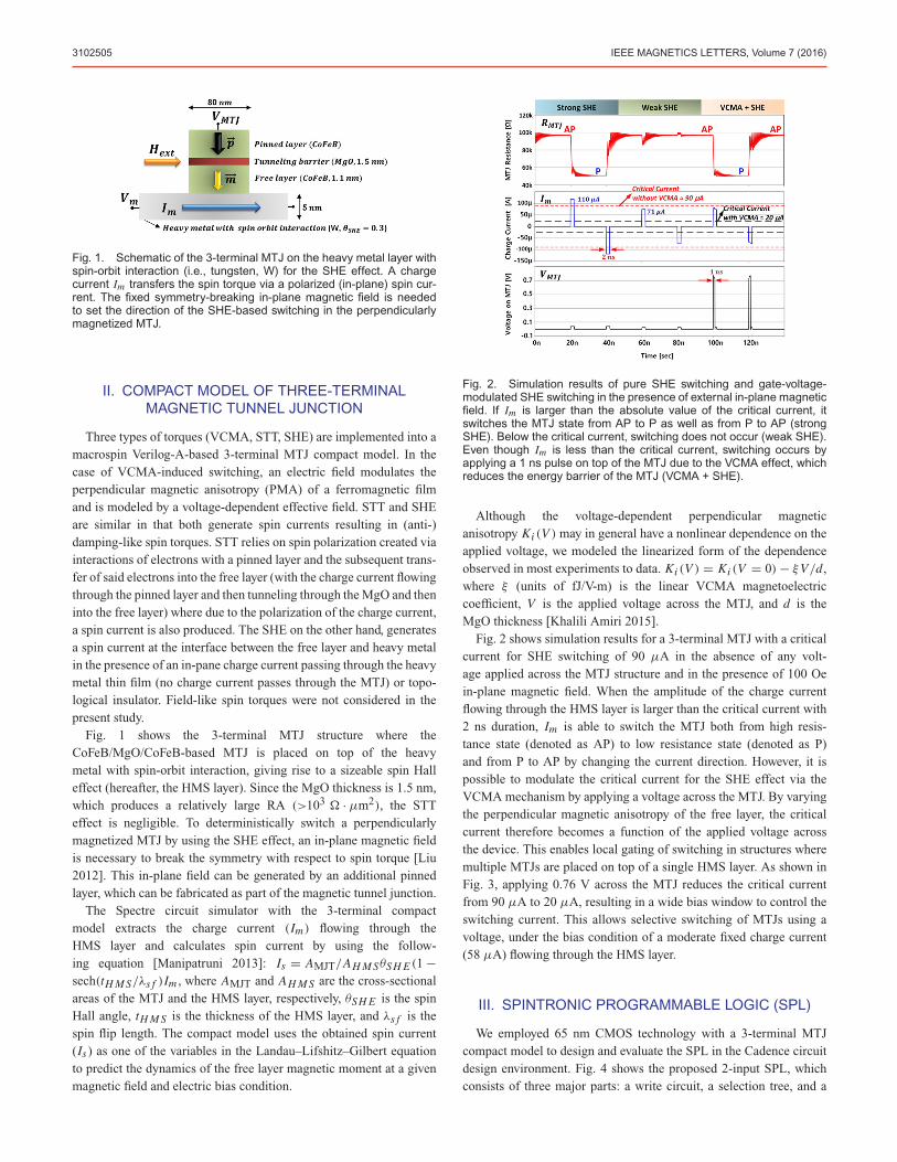
Fig. 1. Schematic of the 3-terminal MTJ on the heavy metal layer withspin-orbit interaction (i.e., tungsten, W) for the SHE effect. A chargecurrent Im transfers the spin torque via a polarized (in-plane) spin cur-rent. The fixed symmetry-breaking in-plane magnetic field is neededto set the direction of the SHE-based switching in the perpendicularlymagnetized MTJ.
II. COMPACT MODEL OF THREE-TERMINALMAGNETIC TUNNEL JUNCTION
Three types of torques (VCMA, STT, SHE) are implemented into amacrospin Verilog-A-based 3-terminal MTJ compact model. In thecase of VCMA-induced switching, an electric field modulates theperpendicular magnetic anisotropy (PMA) of a ferromagnetic filmand is modeled by a voltage-dependent effective field. STT and SHEare similar in that both generate spin currents resulting in (anti-)damping-like spin torques. STT relies on spin polarization created viainteractions of electrons with a pinned layer and the subsequent trans-fer of said electrons into the free layer (with the charge current flowingthrough the pinned layer and then tunneling through the MgO and theninto the free layer) where due to the polarization of the charge current,a spin current is also produced. The SHE on the other hand, generatesa spin current at the interface between the free layer and heavy metalin the presence of an in-pane charge current passing through the heavymetal thin film (no charge current passes through the MTJ) or topo-logical insulator. Field-like spin torques were not considered in thepresent study.
Fig. 1 shows the 3-terminal MTJ structure where theCoFeB/MgO/CoFeB-based MTJ is placed on top of the heavymetal with spin-orbit interaction, giving rise to a sizeable spin Halleffect (hereafter, the HMS layer). Since the MgO thickness is 1.5 nm,which produces a relatively large RA (>103 � · μm2), the STTeffect is negligible. To deterministically switch a perpendicularlymagnetized MTJ by using the SHE effect, an in-plane magnetic fieldis necessary to break the symmetry with respect to spin torque [Liu2012]. This in-plane field can be generated by an additional pinnedlayer, which can be fabricated as part of the magnetic tunnel junction.
The Spectre circuit simulator with the 3-terminal compactmodel extracts the charge current (Im) flowing through theHMS layer and calculates spin current by using the follow-ing equation [Manipatruni 2013]: Is = AMJT/AH M SθSH E (1 −sech(tH M S/λs f )Im , where AMJT and AH M S are the cross-sectionalareas of the MTJ and the HMS layer, respectively, θSH E is the spinHall angle, tH M S is the thickness of the HMS layer, and λs f is thespin flip length. The compact model uses the obtained spin current(Is ) as one of the variables in the Landau–Lifshitz–Gilbert equationto predict the dynamics of the free layer magnetic moment at a givenmagnetic field and electric bias condition.
Fig. 2. Simulation results of pure SHE switching and gate-voltage-modulated SHE switching in the presence of external in-plane magneticfield. If Im is larger than the absolute value of the critical current, itswitches the MTJ state from AP to P as well as from P to AP (strongSHE). Below the critical current, switching does not occur (weak SHE).Even though Im is less than the critical current, switching occurs byapplying a 1 ns pulse on top of the MTJ due to the VCMA effect, whichreduces the energy barrier of the MTJ (VCMA + SHE).
Although the voltage-dependent perpendicular magneticanisotropy Ki (V ) may in general have a nonlinear dependence on theapplied voltage, we modeled the linearized form of the dependenceobserved in most experiments to data. Ki (V ) = Ki (V = 0) − ξV/d ,where ξ (units of fJ/V-m) is the linear VCMA magnetoelectriccoefficient, V is the applied voltage across the MTJ, and d is theMgO thickness [Khalili Amiri 2015].
Fig. 2 shows simulation results for a 3-terminal MTJ with a criticalcurrent for SHE switching of 90 μA in the absence of any volt-age applied across the MTJ structure and in the presence of 100 Oein-plane magnetic field. When the amplitude of the charge currentflowing through the HMS layer is larger than the critical current with2 ns duration, Im is able to switch the MTJ both from high resis-tance state (denoted as AP) to low resistance state (denoted as P)and from P to AP by changing the current direction. However, it ispossible to modulate the critical current for the SHE effect via theVCMA mechanism by applying a voltage across the MTJ. By varyingthe perpendicular magnetic anisotropy of the free layer, the criticalcurrent therefore becomes a function of the applied voltage acrossthe device. This enables local gating of switching in structures wheremultiple MTJs are placed on top of a single HMS layer. As shown inFig. 3, applying 0.76 V across the MTJ reduces the critical currentfrom 90 μA to 20 μA, resulting in a wide bias window to control theswitching current. This allows selective switching of MTJs using avoltage, under the bias condition of a moderate fixed charge current(58 μA) flowing through the HMS layer.
III. SPINTRONIC PROGRAMMABLE LOGIC (SPL)
We employed 65 nm CMOS technology with a 3-terminal MTJcompact model to design and evaluate the SPL in the Cadence circuitdesign environment. Fig. 4 shows the proposed 2-input SPL, whichconsists of three major parts: a write circuit, a selection tree, and a

IEEE MAGNETICS LETTERS, Volume 7 (2016) 3102505
Fig. 3. Switching probability as a function of current (Im ) amplitudeand applied voltage (VMJT). The switching probability for each condi-tion was extracted from 1,000 attempts based on the 3-terminal MTJcompact model simulation. As the applied voltage (VMJT) increases,less current (Im ) is necessary to switch the MTJ state.
Fig. 4. Schematic of the proposed 2-input spintronic programmablelogic (SPL). The truth table of a 2-input function is stored into 4 DataMTJs (MJT1∼MJT4). In the write mode, M1 and M2 turn on to generatecurrent Im for SHE and VMJT is applied for the VCMA effect throughBLs. In the logic operation mode, one of the Data MTJs is selectedbased on the input signal A and B. The state of the selected MTJ isdetected by a current conveyer, generating a stable logic value “high”(AP) or “low” (P).
current conveyer. The write circuit is used to configure the data MTJs(MJT1∼MJT4). For instance, to configure the XOR logic function a58 μA charge current (Im ), provided by the write circuit (M1, M2),flows through the HMS layer to generate the SHE and a ∼0.5 V pulse(VMJT) is simultaneously applied on the BL2 and the BL3, chang-ing MTJ2 and MTJ3 from AP to P via the gate-voltage-modulatedSHE switching, hence realizing a parallel write configuration. Thewrite (configuration) operation is followed by two logic operationsseparated by the standby mode (power off) as shown in Fig. 5.
The selection tree is used for the logic operation to choose one ofthe current paths, selecting an MTJ associated with the input bits of Aand B. The current conveyers, composed of two transistors (M4, M5)and two AP state MTJs (MTJ5, MTJ6), increase the sensing marginby using the feedback loop. The detailed operation is described inSection IV.
Based on the configuration of MJT1∼MJT4, the SPL can performany type of combinational and sequential logic functions by combin-ing a flip-flop. One can increase the number of inputs of the SPL byadding more MTJs, realizing more sophisticated logic functions. It is
Fig. 5. Write and logic operation of the proposed 2-input SPL. TheMTJ2 and MTJ3 are switched from AP to P due to the 2 ns durationof the charge current Im ≈58 μA with 0.44 V pulse on BL2 and BL3.During the logic operation, MTJs are consecutively selected based ontwo inputs, A and B, and an OUT, which corresponds with the storeddata in MTJs, is available at the rising edge of CLK. After power off andon, the same logic function is realized due to the non-volatile nature ofMTJs.
noteworthy that the same logic operation can be resumed after return-ing from the standby mode (power off) due to non-volatile MTJs,thus achieving zero standby power and instant-on recovery withoutnecessitating a data fetch from external memory.
IV. PERFORMANCE
A. Sensing Margin
The sensing margin is limited by intrinsic characteristics of theMTJs (in particular the tunnel magnetoresistance, TMR), as well asby circuit design parameters and the sensing scheme used. Previousworks have shown that 0.18 V sensing margin can be achieved basedon 1T-1MTJ topology with 200% TMR and a 65 nm technology [Song2011]. In the proposed circuit, as shown in Fig. 4, the sensing mar-gin is defined by the voltage difference between the REF node andthe SENS node. To maximize the sensing margin, a modified versionof the current conveyer circuit is implemented into the SPL [Koike2011]. Based on an achieved TMR of 100%, the SPL achieves a 0.8 Vsensing margin in this work.
The logic operation based on the current conveyer circuit is as fol-lows: the R_Enable rises up to 1.0 V and pre-charges the REF nodeand the SENS node at a certain voltage level, which slightly turns M4and M5 on. Simultaneously, both REF and SENS nodes become virtu-ally shorted by turning M3 on, as shown in Fig. 6. Once M3 is turnedoff, the potential of the REF node and SENS node are determinedby the strength of the pull-up and pull-down paths. If the selectedMTJ has AP, which is higher than Rre f , the SENS node is dischargedmuch faster than the REF node. The reduced potential of the SENSnode leads M5 to the subthreshold region, discharging the REF nodeslowly. These events are continuously repeated through the feedbackloop until the circuit clearly distinguishes the state of MTJs; AP andP cause “high” and “low” on PREOUT , respectively, as shown inFig. 6.

3102505 IEEE MAGNETICS LETTERS, Volume 7 (2016)
Fig. 6. Simulation of the sensing margin during the logic operation.Because of the current conveyer (M4, M5), a 0.81 V sensing margin isachieved. To execute logic operation, M3 is turned on by INITIAL for0.5 ns, causing the equipotential between REF and SENS node. Afterturning M3 off, the potential of the SENS node is determined by thestate of the selected MTJ; AP makes SENS node “low”, and P makes it“high”.
Fig. 7. An applied voltage VMJT induces the VCMA effect, causing amodulation of the critical current for spin Hall effect switching. In thisstructure, write energy and time require 28.7 fJ/bit and 2 ns, respec-tively. The amount of dynamic power for the logic operation is below20 μW. The SPL consumes zero power during sleep mode (power-offmode).
B. Power Consumption and Area
The configuration energy depends on various factors: the PMA(Ki = 1.005 × 10⁻³ J/m2), VCMA coefficient (ξ = 37 fJ/Vm), sat-uration magnetization (MS = 1.2 × 10⁶ A/m), spin Hall angle(θSH E = 0.3), and parasitic loading of the circuit. Based on the aboveassumptions with the compact model simulation, the switching energyof an MTJ via gate-voltage-modulated SHE switching was extractedand found to be 28.7 fJ/bit, as shown in Fig. 7.
For dynamic logic operation, the circuit consumes below 20 μWwith 1 GHz speed, which is similar to that of the conventional SRAM-based LUT. However, it can achieve zero power consumption duringsleep mode due to the non-volatility of MTJs. The total power dissipa-tion is thus determined by the duty cycle, i.e., the ratio of sleep modeto active mode.
Fig. 8. Area comparison of different types of LUT. The proposedSPL is the most area-efficient structure compared to both SRAM andSTT-RAM-based LUTs. As the number of inputs increases, the areaefficiency of the proposed SPL also improves.
The 2-input SPL can achieve 35% and 28% area reduction com-pared to SRAM and STT-RAM-based 2-input programmable logic,respectively. This is obtained by replacing a 6-transistor SRAM cellwith an MTJ and using the minimum size of transistors for the writecircuit. For these reasons, as the number of inputs increase, the pro-posed SPL can have more of an advantage in terms of area as shownin Fig. 8.
V. CONCLUSION
In this letter, we have presented an SPL architecture based on 3-terminal MTJs, with combined SHE and VCMA operation for logicapplications, where the logic function is determined by the config-uration of the MTJ states. The configuration step can be executedin a parallel manner via the gate-voltage-modulated spin Hall effectswitching, achieving high speed (×100) and reducing the area for thewrite circuit (up to 61%). The SPL performs data processing withGHz clock speed and achieves zero static power.
ACKNOWLEDGMENT
This work was supported in part by the NSF Nanosystems Engineering ResearchCenter for TANMS. The authors would like to acknowledge the collaboration of thisresearch with KACST via the CEGN.
REFERENCES
Huai Y, Albert F, Nguyen P, Pakala M, Valet T (2004), “Observation of spin-transferswitching in deep submicron-sized and low-resistance magnetic tunnel junctions,”Appl. Phys. Lett., vol. 84, pp. 3118–3120, doi: 10.1063/1.1707228.
Ikeda S, Miura K, Yamamoto H, Mizunuma K, Gan H D, Endo M, Janai S, Hayakawa J,Matsukura F, Ohno H (2010), “A perpendicular-anisotropy CoFeB–MgO magnetictunnel junction,” Nat. Mater., vol. 9, pp. 721–724, doi: 10.1038/nmat2804.
Kanai S, Nakatani Y, Yamanouchi M, Ikeda S, Sato H, Matsukura F, Ohno H (2014),“Magnetization switching in a CoFeB/MgO magnetic tunnel junction by combiningspin-transfer torque and electric field-effect,” Appl. Phys. Lett., vol. 104, 212406, doi:10.1063/1.4880720.
Khalili Amiri P, Alzate J G, Cai X Q, Ebrahimi F, Hu Q, Wong K, Grezes C, Lee H,Yu G, Li X, Akyol M, Shao Q, Katine J A, Langer J, Ocker B, Wang K L (2015),“Electric-field-controlled magnetoelectric RAM: Progress, challenges, and scaling,”IEEE Trans. Magn., vol. 51, 3401507, doi: 10.1109/TMAG.2015.2443124.
Koike H, Endoh T (2011), “A new sensing scheme with high signal margin suitable forspin-transfer torque RAM,” Int. Symp. VLSI Technology, Systems and Applications(VLSI-TSA), Hsinchu, Taiwan, pp. 56–57, doi: 10.1109/VTSA.2011.5872230.

IEEE MAGNETICS LETTERS, Volume 7 (2016) 3102505
Kuon I, Rose J (2007), “Measuring the gap between FPGAs and ASICs,” IEEETrans. Comput.-Aid. Design Integr. Circuits Syst., vol. 26, pp. 203–215, doi:10.1109/TCAD.2006.884574.
Lee H, Alzate J, Dorrance R, Cai X, Markovic D, Khalili Amiri P, Wang K (2014),“Design of a fast and low-power sense amplifier and writing circuit for high-speedMRAM,” IEEE Trans. Magn., vol. 51, 3400507, doi: 10.1109/TMAG.2014.2367130.
Liauw Y Y, Zhang Z, Kim W, El Gamal A, Wong S S (2012), “Nonvolatile 3D-FPGA withmonolithically stacked RRAM-based configuration memory,” 2012 IEEE Int. Solid-State Circuits Conf. (ISSCC) Dig., pp. 406–408, doi: 10.1109/ISSCC.2012.6177067.
Liu L, Lee O J, Gudmundsen T J, Ralph D C, Buhrman R A (2012), “Current-induced switching of perpendicularly magnetized magnetic layers using spintorque from the spin Hall effect,” Phys. Rev. Lett., vol. 109, 096602, doi:10.1103/PhysRevLett.109.096602.
Manipatruni S, Nikonov D E, Young I A (2014), “Energy-delay performance of giant spinHall effect switching for dense magnetic memory,” Appl. Phys. Expr., vol. 7, 103001,doi: 10.7567/APEX.7.103001.
Masui S, Ninomiya T, Oura M, Yokozeki W, Mukaida K, Kawashima S (2003), “Aferroelectric memory-based secure dynamically programmable gate array,” IEEE J.Solid-State Circuits, vol. 38, pp. 715–725, doi: 10.1109/JSSC.2003.810034.
Shiota Y, Nozaki T, Bonell F, Murakami S, Shinjo T, Suzuki Y (2012), “Inductionof coherent magnetization switching in a few atomic layers of FeCo using voltagepulses,” Nat. Mater., vol. 11, pp. 39–43, doi: 10.1038/nmat3172.
Song J-W, Kim J, Kang S H, Yoon S-S, Jung S-O (2011), “Sensing margin trend withtechnology scaling in MRAM,” Int. J. Circuit Theory Applicat., vol. 39, pp. 313–325,doi: 10.1002/cta.635.
Suzuki D, Natsui M, Endoh T, Ohno H, Hanyu T (2012), “Six-input lookup table cir-cuit with 62% fewer transistors using nonvolatile logic-in-memory architecture withseries/parallel-connected magnetic tunnel junctions,” J. Appl. Phys., vol. 111, 07E318,doi: 10.1063/1.3672411.
Tehrani S, Slaughter J M, Deherrera M, Engel B N, Rizzo N D, Salter J, Durlam M,Dave R W, Janesky J, Butcher B, Smith K, Grynkewich G (2003), “Magnetoresistiverandom access memory using magnetic tunnel junctions,” Proc. IEEE, vol. 91,pp. 703–714, doi: 10.1109/JPROC.2003.811804.