SIwave-DC · 2019-08-08 · ANSYS SIwave-DC outfi ts you to confi dently predict DC power and...
4
SIwave-DC Realize Your Product Promise ™
Transcript of SIwave-DC · 2019-08-08 · ANSYS SIwave-DC outfi ts you to confi dently predict DC power and...

SIwave-DC
Realize Your Product Promise™
ANSYSSIwave-DCoutfitsyoutoconfidentlypredictDCpowerandvoltagelossforchip–package–systems.
ANSYS SIwave-DC™ analyzes entire printed circuit boards (PCBs) and integrated circuit (IC) packages prevalent in modern electronic products. SIwave-DC accurately predicts failure risks within a design, such as DC voltage drop and power loss per layer, along with DC resistance of power planes, ground planes and signal traces. These capabilities make it an eff ective tool to perform pre-layout power distribution network analysis and reduce post-layout power delivery problems.
DC AnalysisSIwave-DC employs a specialized 3-D fi nite element fi eld solver with adaptive meshing to compute DC currents and voltages on PCBs and PKGs — including 3-D simulation of vias, wirebonds, solderballs and solderbumps. Power loss is calculated per layer along with a resistive network that can be used to make quick design
tradeoff s. These predictive simulations ensure that the power distribution network (PDN) can source enough current to ICs within the PCB or PKG.
Automatic Adaptive Meshing Automatic adaptive meshing allows users to benefi t from the highly accurate fi nite element method without having to build and refi ne a mesh. The user specifi es only the geometry, material properties and desired output. This proven technology eliminates the meshing process and makes advanced numerical analysis practical for all levels of your organization.
Parametric StudiesUsing SIwave-DC, engineers can perform what-if topology studies to determine proper copper weighting and placement of power/ground planes, via location, via plating thickness and wirebond sizes to ensure an optimal power delivery system.
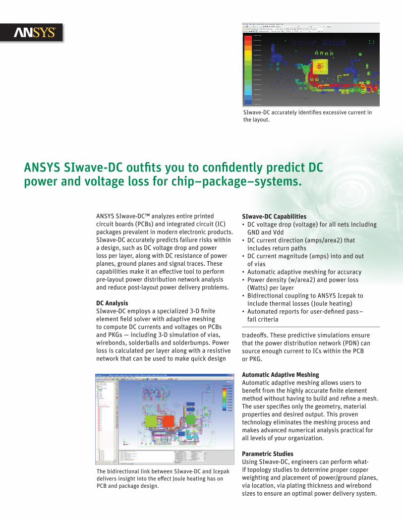
SIwave-DC accurately identifi es excessive current in the layout.
The bidirectional link between SIwave-DC and Icepak delivers insight into the eff ect Joule heating has on PCB and package design.
SIwave-DC Capabilities• DC voltage drop (voltage) for all nets including
GND and Vdd• DC current direction (amps/area2) that
includes return paths • DC current magnitude (amps) into and out
of vias• Automatic adaptive meshing for accuracy• Power density (w/area2) and power loss
(Watts) per layer• Bidirectional coupling to ANSYS Icepak to
include thermal losses (Joule heating)• Automated reports for user-defi ned pass–
fail criteria
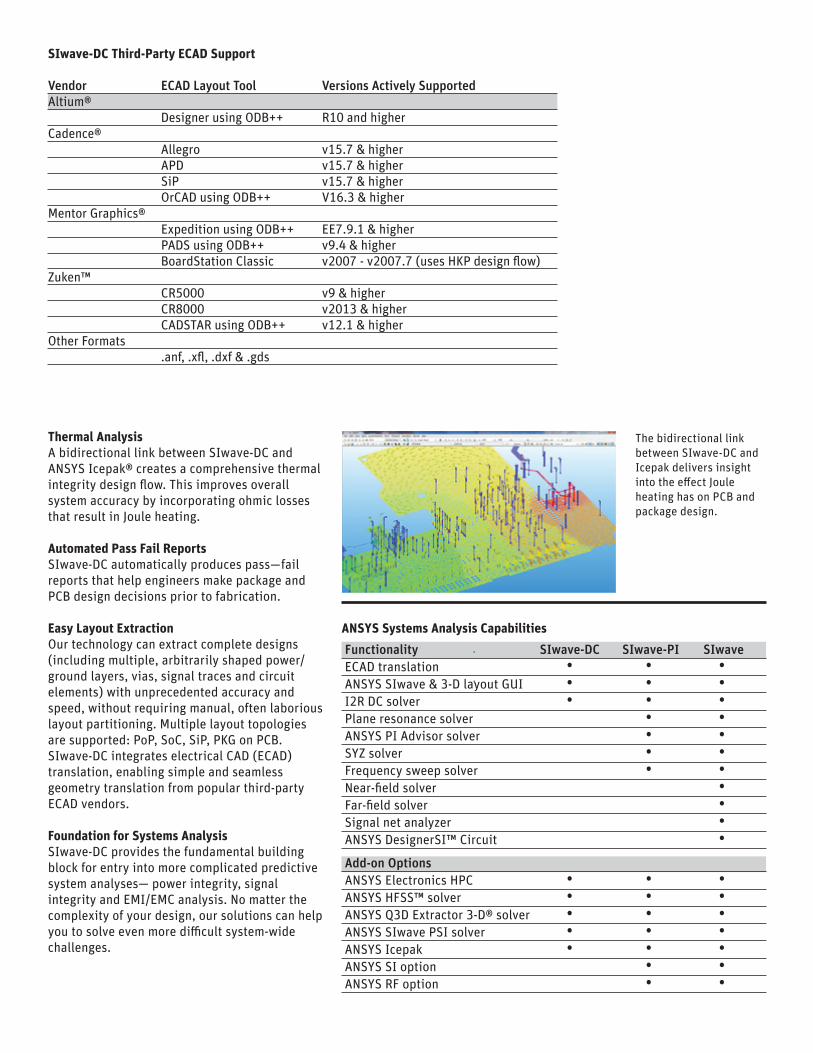
The bidirectional link between SIwave-DC and Icepak delivers insight into the effect Joule heating has on PCB and package design.
SIwave-DC Third-Party ECAD Support
Vendor ECADLayoutTool VersionsActivelySupportedAltium® Designer using ODB++ R10 and higherCadence® Allegro v15.7 & higher APD v15.7 & higher SiP v15.7 & higher OrCAD using ODB++ V16.3 & higherMentor Graphics® Expedition using ODB++ EE7.9.1 & higher PADS using ODB++ v9.4 & higher BoardStation Classic v2007 - v2007.7 (uses HKP design flow)Zuken™ CR5000 v9 & higher CR8000 v2013 & higher CADSTAR using ODB++ v12.1 & higherOther Formats .anf, .xfl, .dxf & .gds
Thermal AnalysisA bidirectional link between SIwave-DC and ANSYS Icepak® creates a comprehensive thermal integrity design flow. This improves overall system accuracy by incorporating ohmic losses that result in Joule heating.
Automated Pass Fail ReportsSIwave-DC automatically produces pass —fail reports that help engineers make package and PCB design decisions prior to fabrication.
Easy Layout ExtractionOur technology can extract complete designs (including multiple, arbitrarily shaped power/ground layers, vias, signal traces and circuit elements) with unprecedented accuracy and speed, without requiring manual, often laborious layout partitioning. Multiple layout topologies are supported: PoP, SoC, SiP, PKG on PCB. SIwave-DC integrates electrical CAD (ECAD) translation, enabling simple and seamless geometry translation from popular third-party ECAD vendors.
Foundation for Systems AnalysisSIwave-DC provides the fundamental building block for entry into more complicated predictive system analyses— power integrity, signal integrity and EMI/EMC analysis. No matter the complexity of your design, our solutions can help you to solve even more difficult system-wide challenges.
ANSYS Systems Analysis CapabilitiesFunctionality SIwave-DC SIwave-PI SIwave ECAD translation • • • ANSYS SIwave & 3-D layout GUI • • • I2R DC solver • • • Plane resonance solver • • ANSYS PI Advisor solver • • SYZ solver • • Frequency sweep solver • • Near-field solver • Far-field solver • Signal net analyzer • ANSYS DesignerSI™ Circuit •Add-onOptions ANSYS Electronics HPC • • • ANSYS HFSS™ solver • • • ANSYS Q3D Extractor 3-D® solver • • • ANSYS SIwave PSI solver • • • ANSYS Icepak • • • ANSYS SI option • • ANSYS RF option • •

ANSYS is dedicated exclusively to developing engineering simulation software that fosters rapid and innovative product design. Our technology enables you to predict with confi dence that your product will thrive in the real world. For more than 40 years, customers in the most demanding markets have trusted our solutions to help ensure the integrity of their products and drive business success through innovation.
ANSYS and any and all ANSYS, Inc. brand, product, service and feature names, logos and slogans are registered trademarks or trademarks of ANSYS, Inc. or its subsidiaries in the United States or other countries. All other brand, product, service and feature names or trademarks are the property of their respective owners.
MKT
ANSYS, [email protected]
© 2014 ANSYS, Inc. All Rights Reserved.

![Ansys Siwave Brochure 14.0[1]](https://static.fdocuments.us/doc/165x107/544b459aaf7959a8438b51aa/ansys-siwave-brochure-1401.jpg)