Using HFSS with SIwave to Optimize PCB Design
24
1 © 2013 ANSYS, Inc. March 30, 2015 ANSYS Confidential © 2013 ANSYS, Inc. March 30, 2015 ANSYS Confidential Using HFSS with SIwave to Optimize Post-Layout PCB Designs Fisayo Adepetun SI/PI Application Engineer
-
Upload
adefisayo-adepetun -
Category
Documents
-
view
431 -
download
17
Transcript of Using HFSS with SIwave to Optimize PCB Design
1 © 2013 ANSYS, Inc. March 30, 2015 ANSYS Confidential© 2013 ANSYS, Inc. March 30, 2015 ANSYS Confidential
Using HFSS with SIwave to Optimize Post-Layout PCB Designs
Fisayo Adepetun
SI/PI Application Engineer
2 © 2013 ANSYS, Inc. March 30, 2015 ANSYS Confidential© 2013 ANSYS, Inc. March 30, 2015 ANSYS Confidential
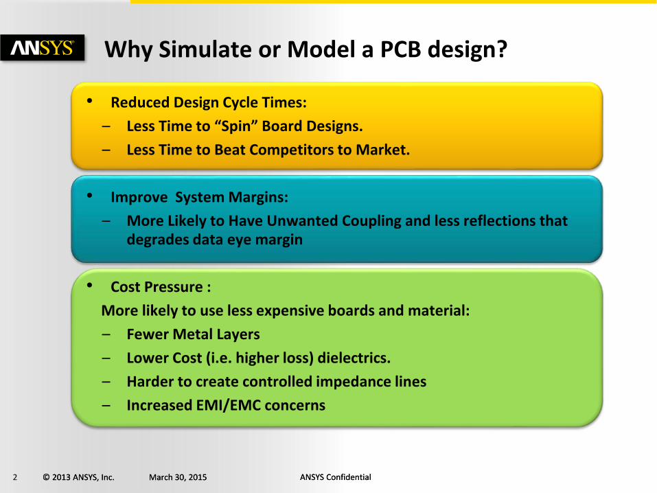
Why Simulate or Model a PCB design?
• Reduced Design Cycle Times:
– Less Time to “Spin” Board Designs.
– Less Time to Beat Competitors to Market.
• Improve System Margins:
– More Likely to Have Unwanted Coupling and less reflections that degrades data eye margin
• Cost Pressure :
More likely to use less expensive boards and material:
– Fewer Metal Layers
– Lower Cost (i.e. higher loss) dielectrics.
– Harder to create controlled impedance lines
– Increased EMI/EMC concerns
3 © 2013 ANSYS, Inc. March 30, 2015 ANSYS Confidential© 2013 ANSYS, Inc. March 30, 2015 ANSYS Confidential
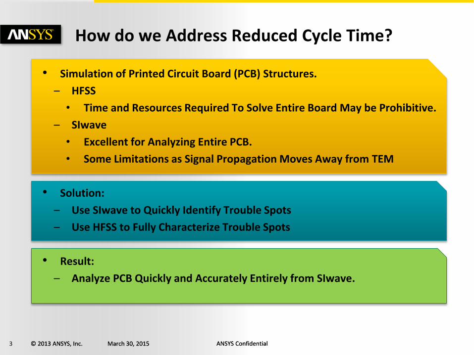
How do we Address Reduced Cycle Time?
• Simulation of Printed Circuit Board (PCB) Structures.
– HFSS
• Time and Resources Required To Solve Entire Board May be Prohibitive.
– SIwave
• Excellent for Analyzing Entire PCB.
• Some Limitations as Signal Propagation Moves Away from TEM
• Solution:
– Use SIwave to Quickly Identify Trouble Spots
– Use HFSS to Fully Characterize Trouble Spots
• Result:
– Analyze PCB Quickly and Accurately Entirely from SIwave.
4 © 2013 ANSYS, Inc. March 30, 2015 ANSYS Confidential© 2013 ANSYS, Inc. March 30, 2015 ANSYS Confidential
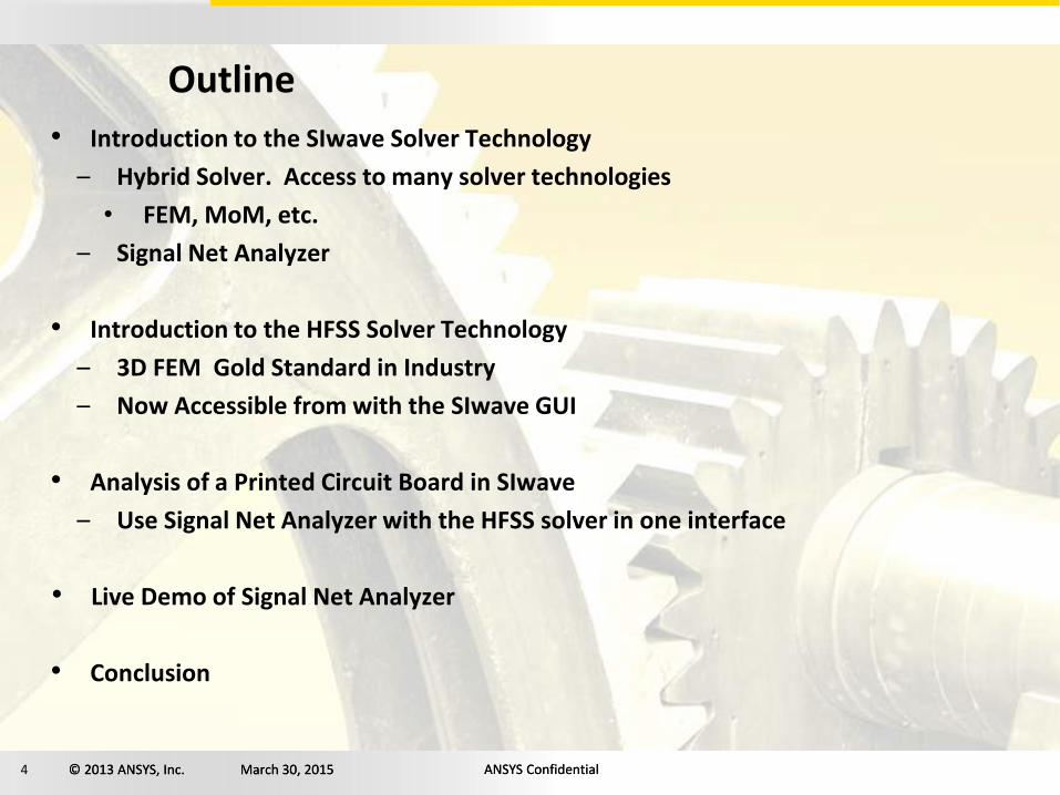
Outline
• Introduction to the SIwave Solver Technology
– Hybrid Solver. Access to many solver technologies
• FEM, MoM, etc.
– Signal Net Analyzer
• Introduction to the HFSS Solver Technology
– 3D FEM Gold Standard in Industry
– Now Accessible from with the SIwave GUI
• Analysis of a Printed Circuit Board in SIwave
– Use Signal Net Analyzer with the HFSS solver in one interface
• Live Demo of Signal Net Analyzer
• Conclusion
5 © 2013 ANSYS, Inc. March 30, 2015 ANSYS Confidential© 2013 ANSYS, Inc. March 30, 2015 ANSYS Confidential
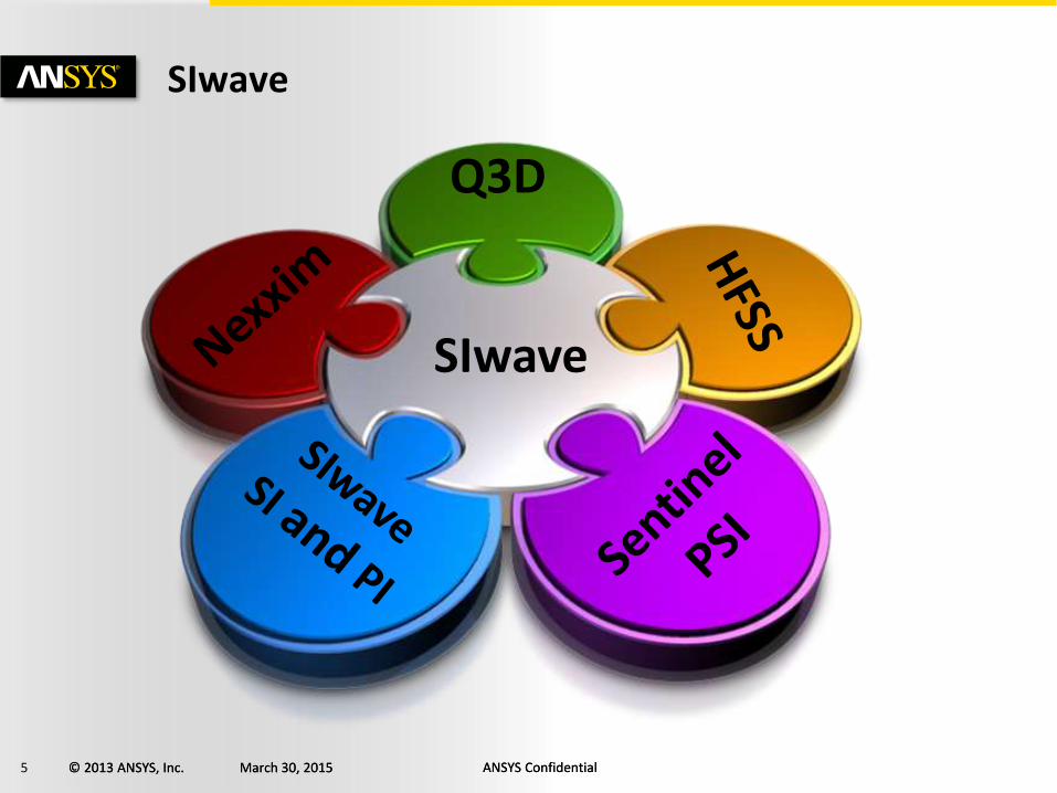
SIwave
SIwave
Q3D
6 © 2013 ANSYS, Inc. March 30, 2015 ANSYS Confidential© 2013 ANSYS, Inc. March 30, 2015 ANSYS Confidential
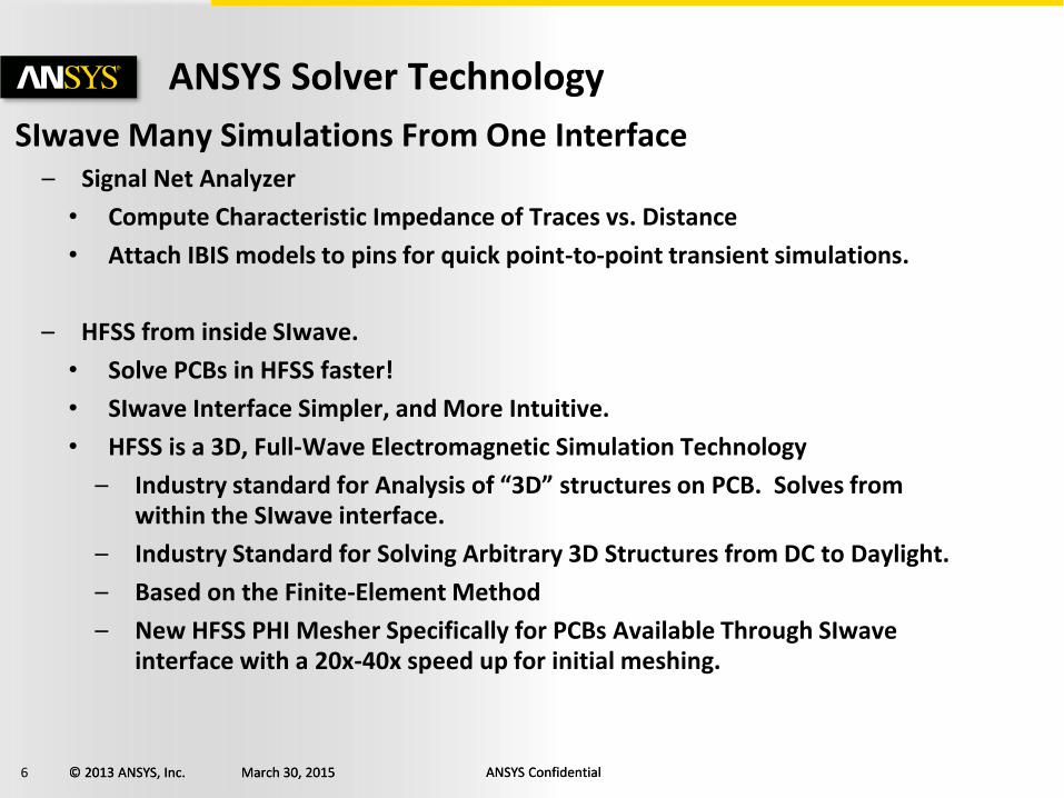
ANSYS Solver Technology
SIwave Many Simulations From One Interface– Signal Net Analyzer
• Compute Characteristic Impedance of Traces vs. Distance
• Attach IBIS models to pins for quick point-to-point transient simulations.
– HFSS from inside SIwave.
• Solve PCBs in HFSS faster!
• SIwave Interface Simpler, and More Intuitive.
• HFSS is a 3D, Full-Wave Electromagnetic Simulation Technology
– Industry standard for Analysis of “3D” structures on PCB. Solves from within the SIwave interface.
– Industry Standard for Solving Arbitrary 3D Structures from DC to Daylight.
– Based on the Finite-Element Method
– New HFSS PHI Mesher Specifically for PCBs Available Through SIwave interface with a 20x-40x speed up for initial meshing.

7 © 2013 ANSYS, Inc. March 30, 2015 ANSYS Confidential© 2013 ANSYS, Inc. March 30, 2015 ANSYS Confidential
Analysis of PCB in Siwave – A DDR3 Case Study
• PCB Layout has DDR3 bus that includes eight (8 bit) byte lanes
• Time and resources prohibit the simulation of all of the byte lanes in HFSS.
• Isolate the worst byte lane to simulate in HFSS using SIwave.
• Need a way to quickly identify the worst case byte lane.

8 © 2013 ANSYS, Inc. March 30, 2015 ANSYS Confidential© 2013 ANSYS, Inc. March 30, 2015 ANSYS Confidential
Analysis of PCB in SIwave
• Close look at Byte group 0: DQ[7:0]
The breakout, open field and dimm field region can be analyzed easily.
9 © 2013 ANSYS, Inc. March 30, 2015 ANSYS Confidential© 2013 ANSYS, Inc. March 30, 2015 ANSYS Confidential
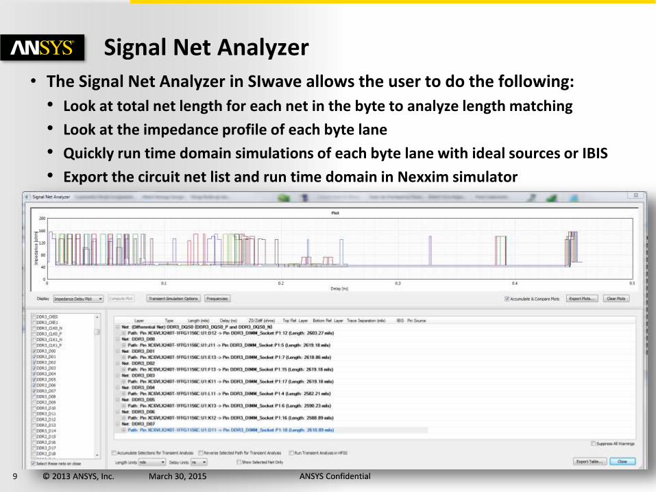
Signal Net Analyzer • The Signal Net Analyzer in SIwave allows the user to do the following:
• Look at total net length for each net in the byte to analyze length matching
• Look at the impedance profile of each byte lane
• Quickly run time domain simulations of each byte lane with ideal sources or IBIS
• Export the circuit net list and run time domain in Nexxim simulator
10 © 2013 ANSYS, Inc. March 30, 2015 ANSYS Confidential© 2013 ANSYS, Inc. March 30, 2015 ANSYS Confidential
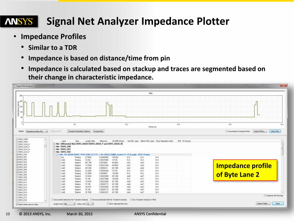
Signal Net Analyzer Impedance Plotter• Impedance Profiles
• Similar to a TDR
• Impedance is based on distance/time from pin
• Impedance is calculated based on stackup and traces are segmented based on their change in characteristic impedance.
Impedance profile of Byte Lane 2
11 © 2013 ANSYS, Inc. March 30, 2015 ANSYS Confidential© 2013 ANSYS, Inc. March 30, 2015 ANSYS Confidential
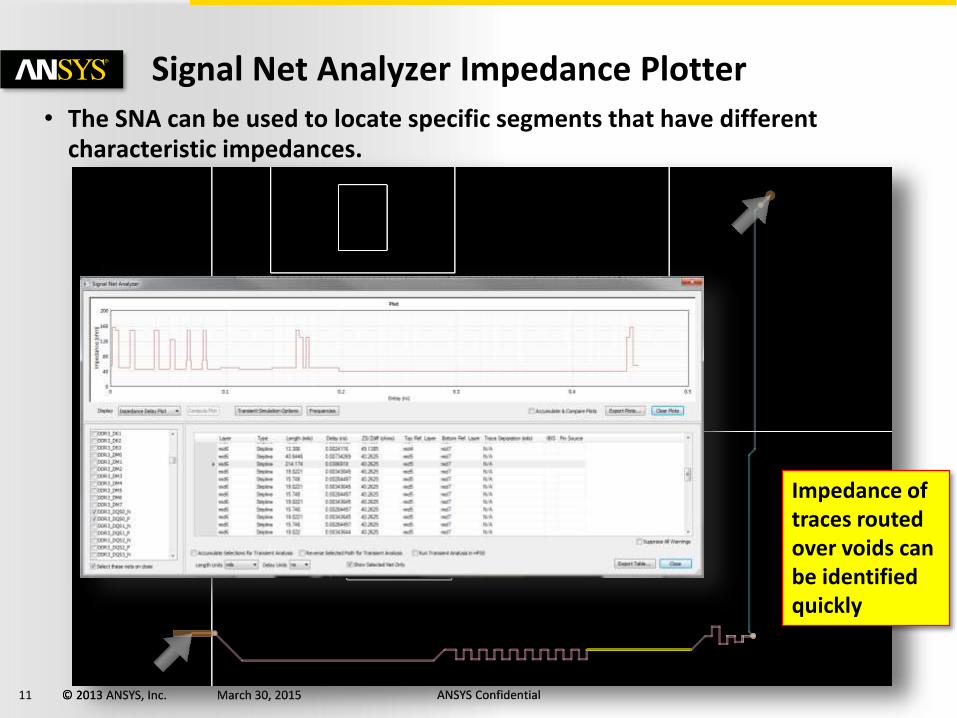
Signal Net Analyzer Impedance Plotter• The SNA can be used to locate specific segments that have different
characteristic impedances.
Impedance of traces routed over voids can be identified quickly

12 © 2013 ANSYS, Inc. March 30, 2015 ANSYS Confidential© 2013 ANSYS, Inc. March 30, 2015 ANSYS Confidential
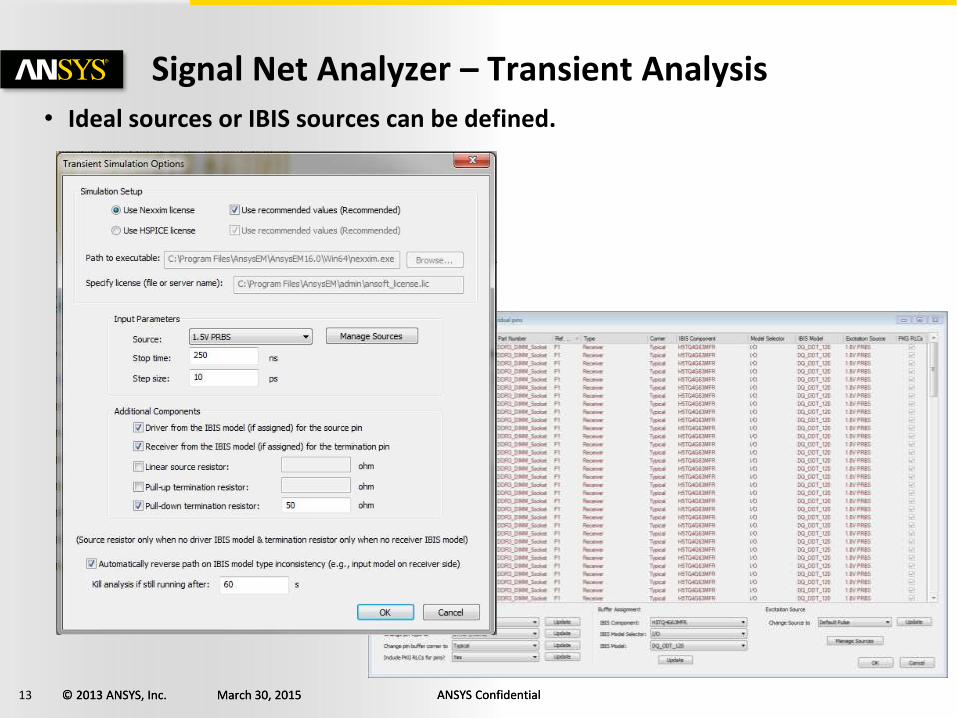
Signal Net Analyzer – Transient Analysis• Quick look at transient response can be run directly from the Signal Net
Analyzer.
Ideal or Ibis sources can be used.
13 © 2013 ANSYS, Inc. March 30, 2015 ANSYS Confidential© 2013 ANSYS, Inc. March 30, 2015 ANSYS Confidential
Signal Net Analyzer – Transient Analysis• Ideal sources or IBIS sources can be defined.
14 © 2013 ANSYS, Inc. March 30, 2015 ANSYS Confidential© 2013 ANSYS, Inc. March 30, 2015 ANSYS Confidential
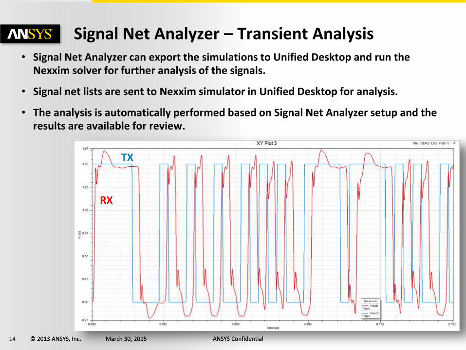
Signal Net Analyzer – Transient Analysis• Signal Net Analyzer can export the simulations to Unified Desktop and run the
Nexxim solver for further analysis of the signals.
• Signal net lists are sent to Nexxim simulator in Unified Desktop for analysis.
• The analysis is automatically performed based on Signal Net Analyzer setup and the results are available for review.
TX
RX
15 © 2013 ANSYS, Inc. March 30, 2015 ANSYS Confidential© 2013 ANSYS, Inc. March 30, 2015 ANSYS Confidential
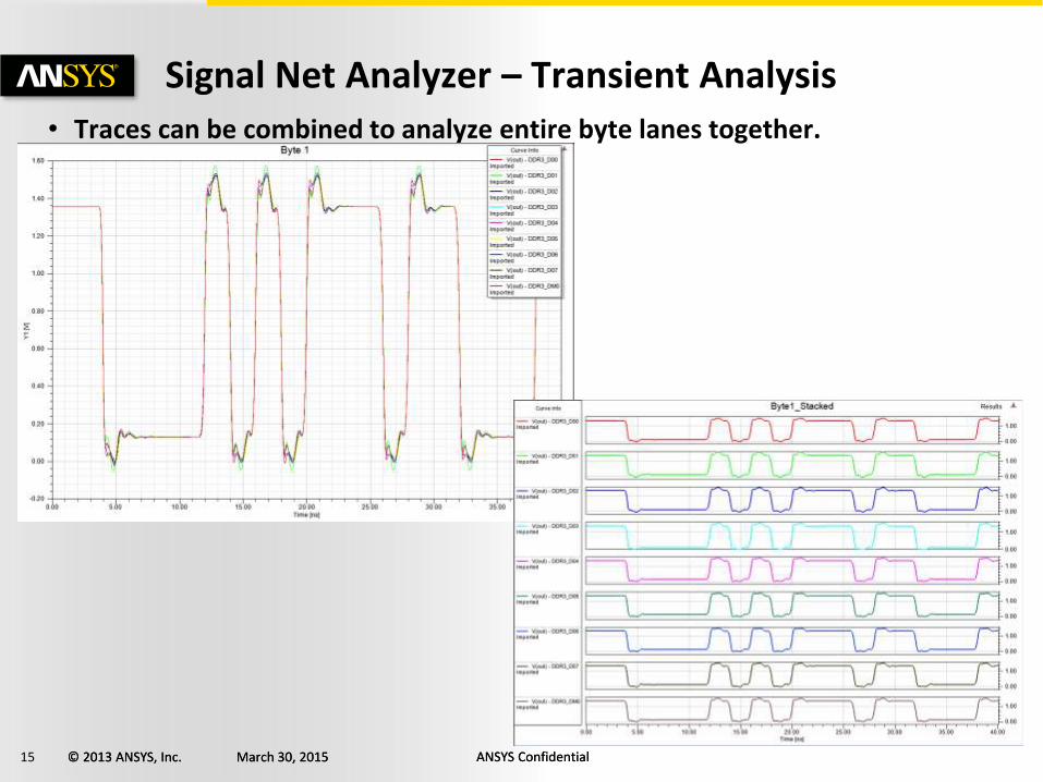
Signal Net Analyzer – Transient Analysis• Traces can be combined to analyze entire byte lanes together.
16 © 2013 ANSYS, Inc. March 30, 2015 ANSYS Confidential© 2013 ANSYS, Inc. March 30, 2015 ANSYS Confidential
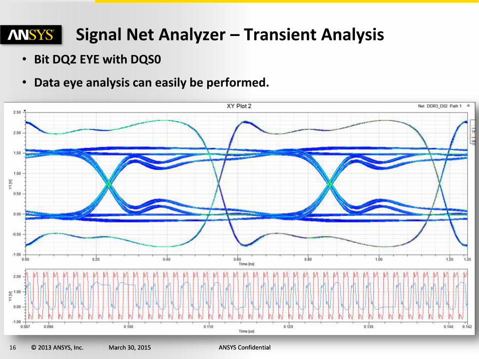
Signal Net Analyzer – Transient Analysis• Bit DQ2 EYE with DQS0
• Data eye analysis can easily be performed.
17 © 2013 ANSYS, Inc. March 30, 2015 ANSYS Confidential© 2013 ANSYS, Inc. March 30, 2015 ANSYS Confidential
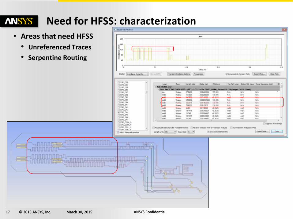
Need for HFSS: characterization• Areas that need HFSS
• Unreferenced Traces
• Serpentine Routing
18 © 2013 ANSYS, Inc. March 30, 2015 ANSYS Confidential© 2013 ANSYS, Inc. March 30, 2015 ANSYS Confidential
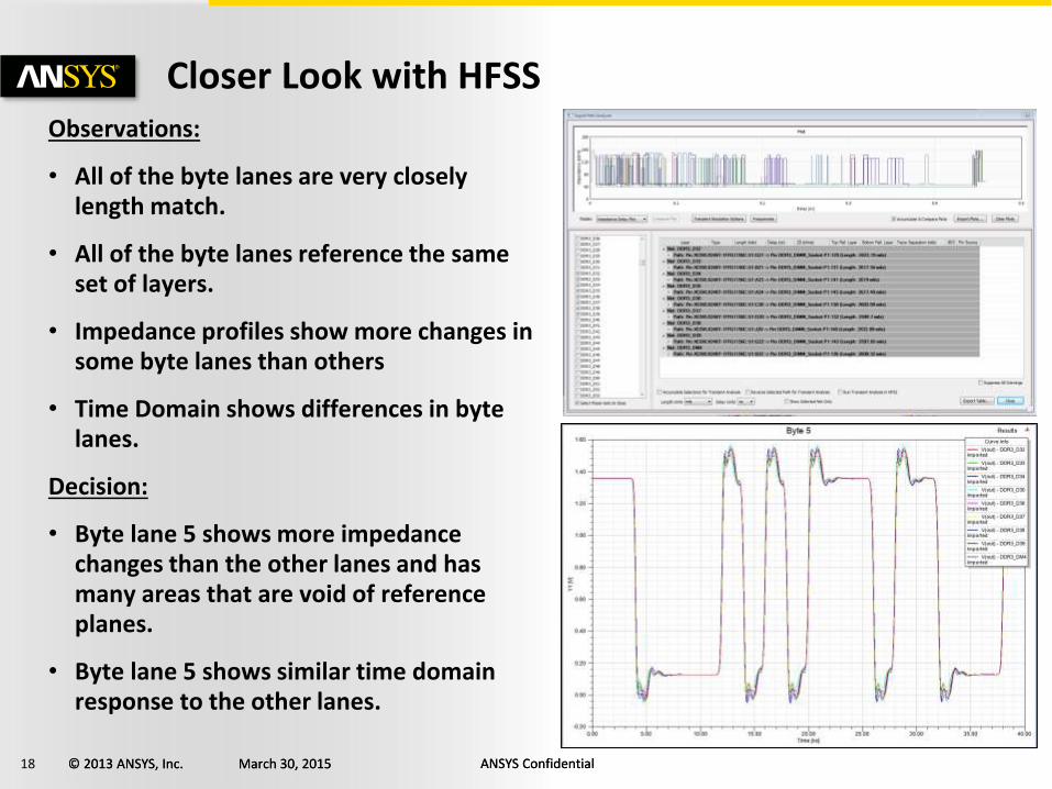
Closer Look with HFSSObservations:
• All of the byte lanes are very closely length match.
• All of the byte lanes reference the same set of layers.
• Impedance profiles show more changes in some byte lanes than others
• Time Domain shows differences in byte lanes.
Decision:
• Byte lane 5 shows more impedance changes than the other lanes and has many areas that are void of reference planes.
• Byte lane 5 shows similar time domain response to the other lanes.
19 © 2013 ANSYS, Inc. March 30, 2015 ANSYS Confidential© 2013 ANSYS, Inc. March 30, 2015 ANSYS Confidential
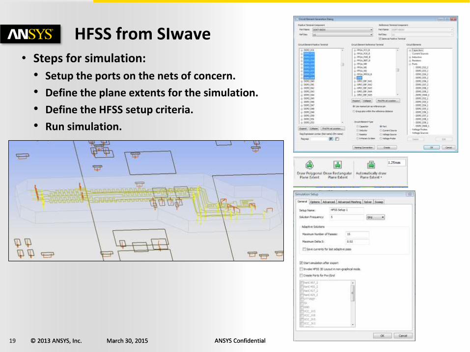
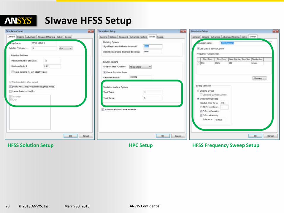
HFSS from SIwave• Steps for simulation:
• Setup the ports on the nets of concern.
• Define the plane extents for the simulation.
• Define the HFSS setup criteria.
• Run simulation.
20 © 2013 ANSYS, Inc. March 30, 2015 ANSYS Confidential© 2013 ANSYS, Inc. March 30, 2015 ANSYS Confidential
SIwave HFSS Setup
HPC SetupHFSS Solution Setup HFSS Frequency Sweep Setup
21 © 2013 ANSYS, Inc. March 30, 2015 ANSYS Confidential© 2013 ANSYS, Inc. March 30, 2015 ANSYS Confidential
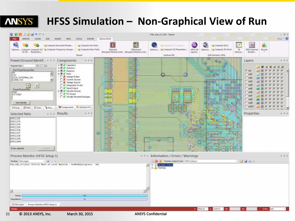
HFSS Simulation – Non-Graphical View of Run
22 © 2013 ANSYS, Inc. March 30, 2015 ANSYS Confidential© 2013 ANSYS, Inc. March 30, 2015 ANSYS Confidential
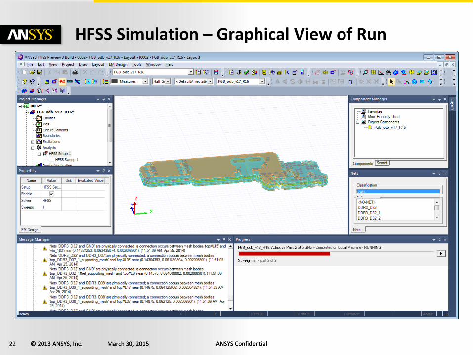
HFSS Simulation – Graphical View of Run
23 © 2013 ANSYS, Inc. March 30, 2015 ANSYS Confidential© 2013 ANSYS, Inc. March 30, 2015 ANSYS Confidential
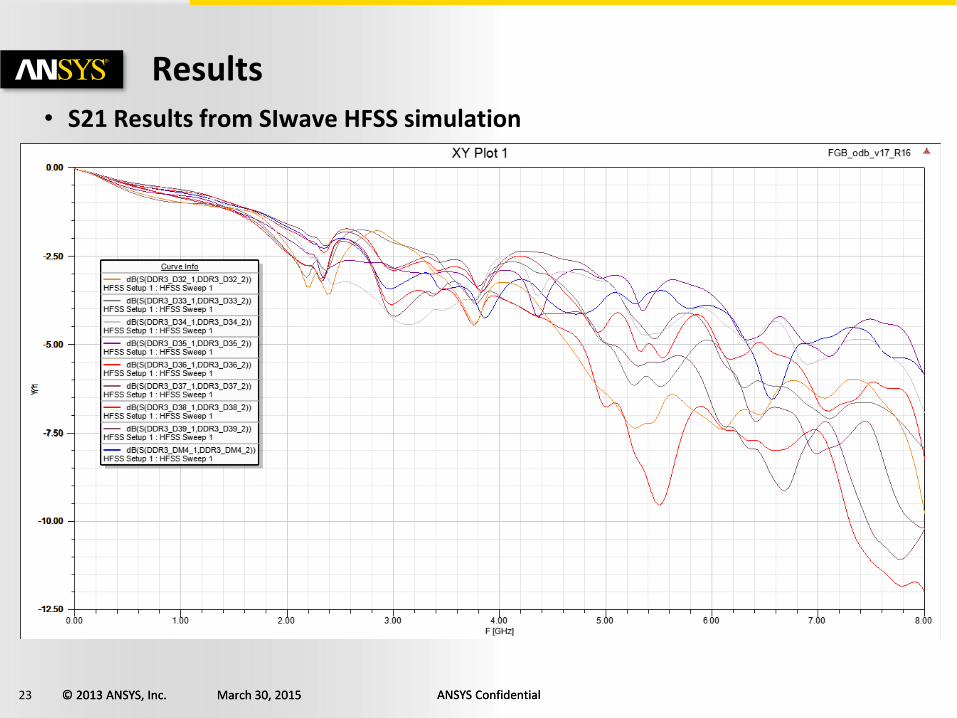
Results• S21 Results from SIwave HFSS simulation
24 © 2013 ANSYS, Inc. March 30, 2015 ANSYS Confidential© 2013 ANSYS, Inc. March 30, 2015 ANSYS Confidential
Conclusion
• Reduced Design Cycle Times Mean Less Time to Get the Design Right.
– Cannot Afford the Time to Spin PCB Many Times.
• Model the PCB Before Manufacturing It
• Use SIwave Signal Net Analyzer to Quickly Identify Trouble Nets
• Use Accuracy of HFSS to Characterize Trouble Nets
– Speed up Simulations with HPC
• Correct Layout Before Manufacturing
• Save Time and Money!
• Be First to Market!