Simple Circuits Inc. SIMPLE SDR...
14
Page 0 Simple Circuits Inc. SIMPLE SDR RECEIVER 80 through 17 Meter General Coverage Receiver © Simple Circuits Inc. 2011 7/8/2011
Transcript of Simple Circuits Inc. SIMPLE SDR...
Page 0
Simple Circuits Inc.
SIMPLE SDR
RECEIVER 80 through 17 Meter General Coverage Receiver
© Simple Circuits Inc. 2011
7/8/2011
Page 1
Simple SDR Receiver
Introduction:
This document describes the installation, how to operate, and theory of operation of the Simple
Circuits Inc. Simple SDR HF radio receiver operating in the 3.5 to 18 MHz range. The receiver
architecture is based on software defined radio techniques and incorporates a Cypress PSoC
CY8C3866 device that contains both analog and digital circuits, thus decreasing the receiver's
component count. This part is far more than just a microcomputer; it also contains software
configurable analog and digital peripherals on a single chip. Cypress calls the family a PSoC in
reference to it being a programmable embedded system-on-chip. The newest series of parts,
which Cypress calls the PSoC 3 family, contains a 67 MHz 8051 class microcomputer, an analog
to digital converter fast enough and with enough resolution for an SDR receiver, and other
valuable functions that are desirable in a receiver design.
The receiver should be used for casual, conversational listening, not a higher performance
receiver for DX use. It was designed to use a minimum number of components, to be physically
small, and easy to operate. An LCD display and controls to select the frequency and modes of
operations was considered, but the design would have fewer parts and cost less if a personal
computer (PC) is used for all user control. Since the PSoC has a USB port, the receiver can
connect to the PC with a USB cable and take power from the PC over the USB cable, saving a
power jack, and external power source. Control of the receiver is accomplished by the receiver
USB port appearing as a standard com port to the PC. The Ham Radio Deluxe (HRD) program
works perfectly to control this receiver.
Page 2
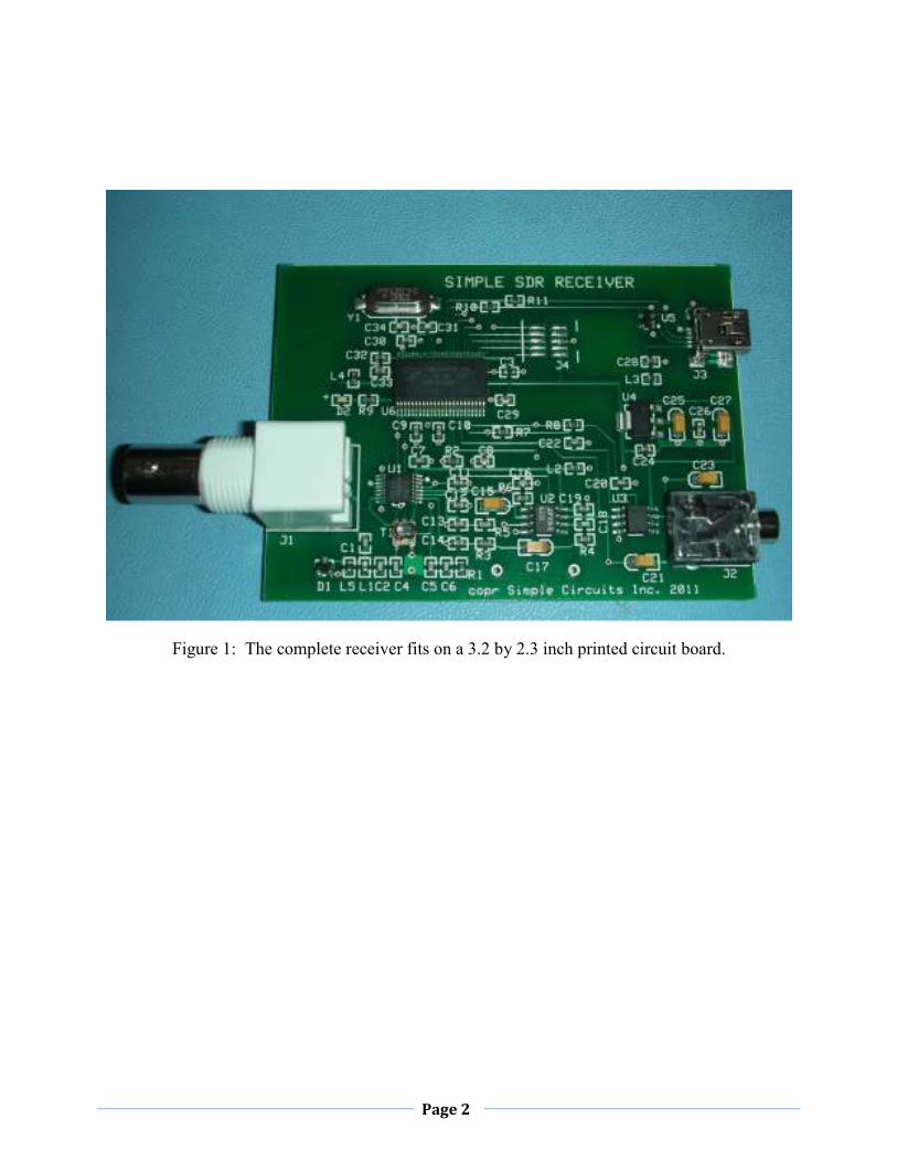
Figure 1: The complete receiver fits on a 3.2 by 2.3 inch printed circuit board.
Page 3
Installation:
Before you connect the USB cable, download the file UARTUSB_CDC.zip and save it on your
computer. Unzip the file, put it in any folder, plug in the USB cable, and the computer will
prompt you to either let it search for the driver, or allow you to specify the driver location. You
will need to specify the location of where you put the file. The receiver has been tested with XP,
Vista, and Windows 7.
Note the com port number that your computer assigned to the receiver. Use that com port
number in Ham Radio Deluxe (HRD). In HRD, add a new radio, and select Elecraft K2 as the
radio type. The speed setting is not important and can be left as the default value.
Operating the Receiver:
To operate the receiver, perform the following steps:
1. Connect the USB cable between a computer USB port and the receiver’s USB connector,
J3. Both power and control are provided by this connection. The PSoC has an internal
USB full speed port. The receiver firmware implements a virtual serial communication
port. When connected to a personal computer, the receiver will look like a serial com
device. Using the standard CDC (communication) drivers that are built into Windows,
the receiver can communicate with Ham Radio Deluxe. The receiver firmware uses the
Elecraft K2 communication protocol.
2. Connect an appropriate antenna to the BNC connector, J1. The antenna should support
the desired receive frequency.
3. Connect an audio amplifier or headset to the audio output connector, J2, of the receiver.
This connector is a stereo connector, but both channels are feed with the same signal.
Therefore, the use of either mono or stereo audio devices are acceptable. The receiver's
audio output will directly drive low impedance headsets. The use of good computer
speakers that have a built-in amplifier and volume adjustment is ideal. There is no
volume control capability in the receiver. Headsets need their own volume adjustments.
The receiver can be continuously tuned from 3.500 MHz to 18.168 MHz (80 through 17 meters).
Using Ham Radio Deluxe to control the radio, the receive frequency, the side band selection, and
audio bandwidth can be selected.
Page 4
There are 4 different receive filter bandwidth selection. Pressing the HRD FILTER button
produces a drop down menu with various options. FL1 is a 2.5 KHz low pass filter, FL2 is a 2.0
KHz low pass filter, FL3 is a 1.5 KHz low pass filter, and FL4 is used for CW and RTTY and is
a 1.0 KHz band pass filter that is 400 Hz wide (+/- 200 Hz).
The attenuator button, ATT will decrease strong stations audio volume by several dB.
Theory of Operation:
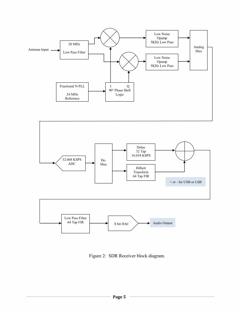
This SDR receiver is built using a quadrature sampling detector, as shown in the block diagram
of figure 2. The quadrature sampling detector is nothing more than a set of analog switches that
are enabled and disabled in the particular sequence that samples the input signal four times for
each cycle of the desired receive frequency. The four samples represent the 0, 90, 180, and 270
degrees of a sine wave. The output of the detector is amplified by a pair of op amp low-pass
filters. After the op amps, the remaining signal processing is performed inside the PSoC
microcomputer using digital processing techniques. The processing will digitize the baseband
signal, remove the undesired sideband from the received signal, limit the bandwidth of the audio,
and then convert the digital samples back into an analog audio signal.
Page 5
Antenna Input
Figure 2: SDR Receiver block diagram.
Low Noise
Opamp
5KHz Low Pass
20 MHz
Low Pass Filter
Analog
Mux
De-
Mux
32.068 KSPS
ADC
Fractional N PLL
24 MHz
Reference
I Q
90° Phase Shift
Logic
Delay
32 Tap
16.034 KSPS
Hilbert
Transform
64 Tap FIR
Low Pass Filter
64 Tap FIR
8 bit DAC
Low Noise
Opamp
5KHz Low Pass
+ or - for USB or LSB
Audio Output
Page 6
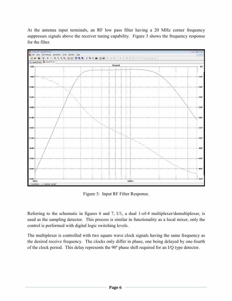
At the antenna input terminals, an RF low pass filter having a 20 MHz corner frequency
suppresses signals above the receiver tuning capability. Figure 3 shows the frequency response
for the filter.
Figure 3: Input RF Filter Response.
Referring to the schematic in figures 6 and 7, U1, a dual 1-of-4 multiplexer/demultiplexer, is
used as the sampling detector. This process is similar in functionality as a local mixer, only the
control is performed with digital logic switching levels.
The multiplexer is controlled with two square wave clock signals having the same frequency as
the desired receive frequency. The clocks only differ in phase, one being delayed by one-fourth
of the clock period. This delay represents the 90º phase shift required for an I/Q type detector.
Page 7
The PSoC has an internal phase lock loop (PLL) circuit that is used to generate higher clock
frequencies from a lower speed clock. The receiver makes use of this circuit to generate the
sampling detector clock signals. An external 24 MHz crystal is connected to the PSoC that is
used as the reference oscillator for the PLL. However, the PSoC PLL only has the ability to
generate frequencies that are integer multiplies of the clock. An additional logic function was
created and added to the programmable digital logic section of the PSoC that modulates the PLL
divider registers. This effectively turns the PLL into a fractional N frequency synthesizer. The
“fractional” term refers to the capability of dividing the PLL feedback signal by a non-integer
number, allowing for a frequency resolution as small as desired. For practical purposes, a 14 bit,
sigma delta modulator constructed as a 2nd order MASH was written in Verilog. This results in a
receiver tuning frequency step size of roughly 50 Hz. When a different frequency is selected, the
PSoC firmware computes a set of PLL values that will be within 50 Hz from the display
frequency.
An external PLL circuit or discrete digital synthesizer chip (DDS) may generate a cleaner clock,
but the advantage of using the internal PLL is obviously component cost savings.
The PLL operates in the 56 to 68 MHz range. A divider function added to the programmable
digital logic section of the PSoC divides the PLL oscillator down to the desired receive
frequency and shifts the phase appropriately between the two output I/Q clocks.
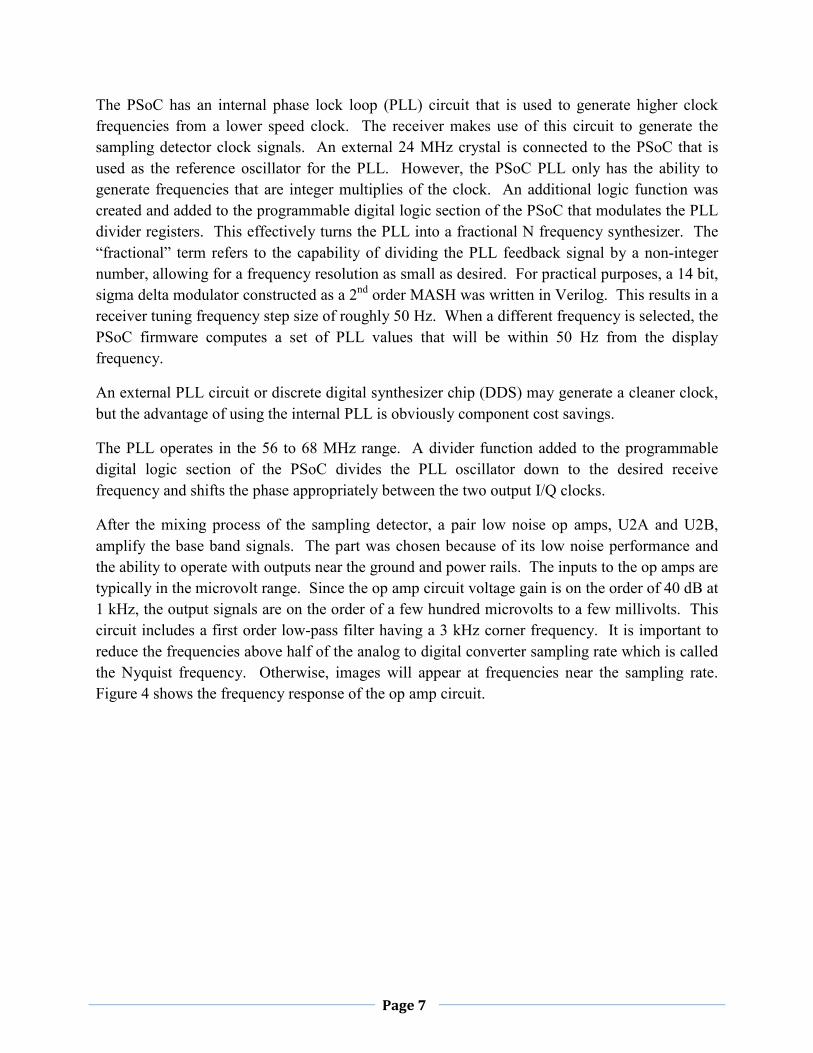
After the mixing process of the sampling detector, a pair low noise op amps, U2A and U2B,
amplify the base band signals. The part was chosen because of its low noise performance and
the ability to operate with outputs near the ground and power rails. The inputs to the op amps are
typically in the microvolt range. Since the op amp circuit voltage gain is on the order of 40 dB at
1 kHz, the output signals are on the order of a few hundred microvolts to a few millivolts. This
circuit includes a first order low-pass filter having a 3 kHz corner frequency. It is important to
reduce the frequencies above half of the analog to digital converter sampling rate which is called
the Nyquist frequency. Otherwise, images will appear at frequencies near the sampling rate.
Figure 4 shows the frequency response of the op amp circuit.
Page 8
Figure 4: Op amp circuit frequency response.
From this point, all of the signal processing is performed in the digital domain, and, specifically,
inside the PSoC, U6.
The PSoC has a single analog to digital converter (ADC). Since there are two base band signals
to process, the I and the Q channels, an analog multiplexer function inside the PSoC is used to
switch one of the two inputs to the ADC input. It is desirable to have a high sample rate and a
high number of bits, but the best tradeoff found was to use the ADC in a 14 bit mode and
sampling at 32,068 samples per second. Since a sample from each input channel is necessary,
the equivalent sample rate per channel is 16,034 samples per second. Therefore, the Nyquist
frequency is almost 8 kHz. The op amp frequency response at 8 kHz is about 10 dB below the
desired passband. This is not great, but leaves room for improvement in a future version.
The PSoC 3 family of parts have an interesting internal hardware feature they call a digital filter
block, or DFB, and it consists of a 24-bit fixed point, programmable limited scope DSP engine.
Page 9
This is a dedicated hardware accelerator block that operates independently of the main 8051
processor. It consists of a dedicated multiplier and accumulator that calculates a 24-bit by 24-bit
multiply 48-bit accumulates in one system clock cycle. It is optimized to implement a direct
form Finite Impulse Response (FIR) filter that approaches a computation rate of one FIR tap for
each clock cycle. This block is used as two independent, 64 tap, digital filters.
Alternating outputs from the ADC are loaded into either a 32 sample long delay line or one of
the two digital filters. This digital filter uses a set of coefficients that form an all-pass filter
having a flat magnitude response, but phase shifts all frequency in its passband by 90°. This is
called a Hilbert filter. Suppressing either the upper or lower sideband is accomplished by phase
shifting the Q channel baseband data and either subtracting or adding the filter output to the
delayed I channel baseband data. The delay is necessary to compensate only for the delays
incurred by the processing of the Hilbert filter. The output of the addition is one of the two
sidebands.
After the removal of the undesired sideband, the data stream is feed into the other half of the
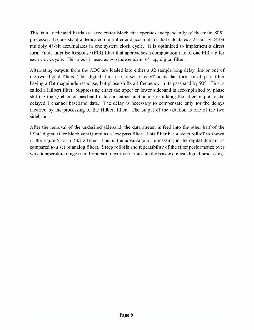
PSoC digital filter block configured as a low-pass filter. This filter has a steep rolloff as shown
in the figure 5 for a 2 kHz filter. This is the advantage of processing in the digital domain as
compared to a set of analog filters. Steep rolloffs and repeatability of the filter performance over
wide temperature ranges and from part to part variations are the reasons to use digital processing.
Page
10
Figure 5: 2 KHz Audio digital low-pass filter response.
The output of the low-pass filter is fed into one of the PSoC’s 8 bit digital to analog converters
(DAC) that converts the data stream back into an analog signal. This signal is buffered with a
unity gain op amp, U3, and passed to the output connector.
Page
11
Performance:
The +5 volt power to the receiver is supplied by the host USB device, and is typically 55 to 60
mA.
The frequency range of operation is controlled by the firmware. The current firmware limits the
tuning to 3.500 MHz to 18.168 MHz. Higher frequencies are beyond the frequency range of the
PSoC internal PLL circuit. Lower frequencies, such as the amateur 160 meter band, were
overloaded from AM broadcast stations.
The minimum discernible signal (MDS) is approximately -117 dBm.
Enclosure Modifications:
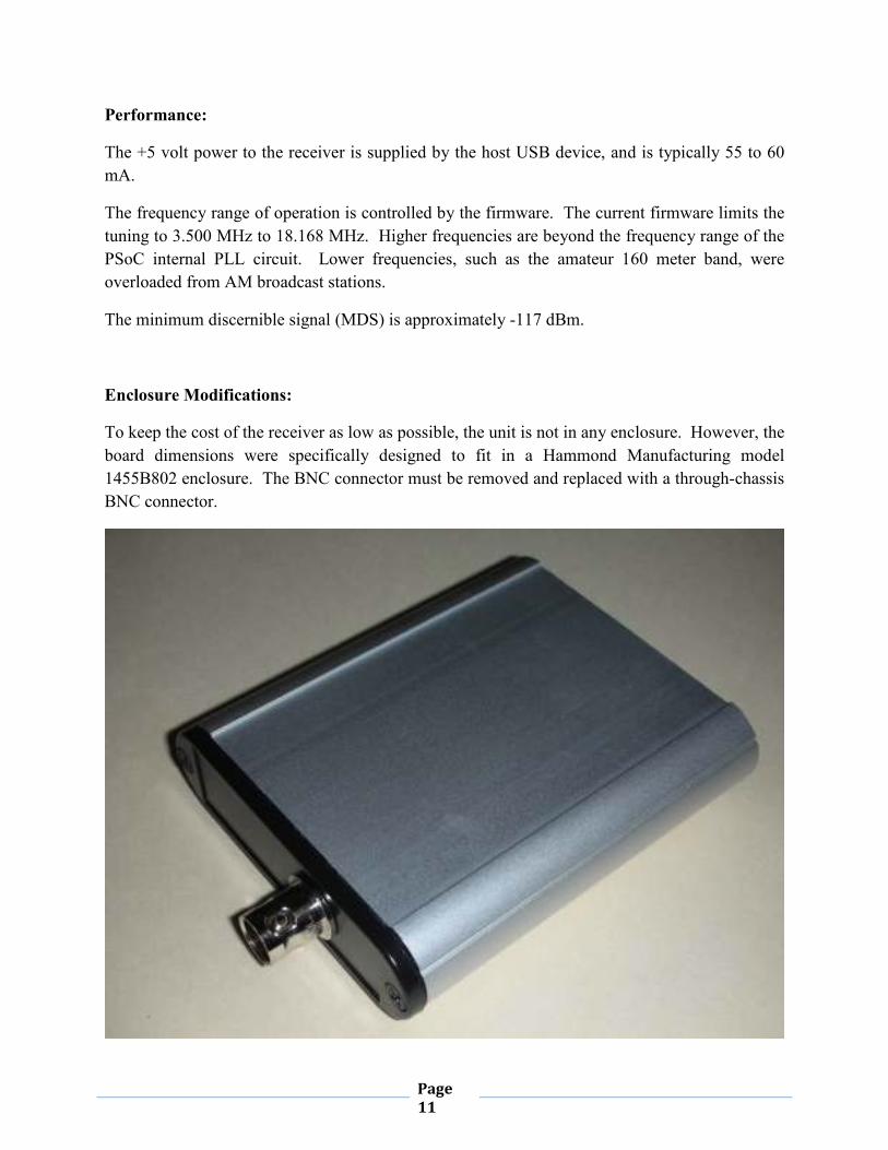
To keep the cost of the receiver as low as possible, the unit is not in any enclosure. However, the
board dimensions were specifically designed to fit in a Hammond Manufacturing model
1455B802 enclosure. The BNC connector must be removed and replaced with a through-chassis
BNC connector.
Page
12
C28
0.1uF
L3
BLM18PG471SN1
J4
CON10A
12
34
56
78
910
3.3V
C3
DNI
3.3V
TP6
TP5
TP3
U6
CY8C3866PVI
P12_2
1
P12_3
2
P0_0
3
P0_1
4
P0_2
5
P0_3
6
VDDIO0
7
P0_4
8
P0_5
9
P0_6
10
P0_7
11
VCCD
12
VSSD
13
VDDD
14
P2_3
15
P2_4
16
VDDIO2
17
P2_5
18
P2_6
19
P2_7
20
VSSB
21
IND
22
VBOOST
23
VBAT
24
P1_1
26
P15_7
35
VDDD
36
VSSD
37
VCCD
38
P15_0
39
P15_1
40
VDDIO3
41
P12_0
42
P12_1
43
P15_2
44
P1_0
25
VCCA
46
VSSA
47
VDDA
48
P1_3
28
P1_5
30
XRES P1_2
27
P1_4
29
P15_3
45
VDDIO1
31
P1_6
32
P1_7
33
P15_6
34
3.3V
ICLK
QCLK
TP1
C30
1.5uF
C10
1.5uF
C29
0.1uF
C9
1.5uF
- +
U3A
LMV358/SO
132
8 4
5V
- +U3B
LMV358/SO
756
8 4
J2
PHONEJACK STEREO
3 2 1
C34
22pF
C20
1000pF
C22
1000pF
R7
33.0K
1%
R8
33.0K
1%
QOUT
IOUT
5V
5V
C31
22pF
3.3V
Title
Size
Document Number
Rev
Date
Sheet
of
File/Schematic Name
Time
Page Name
SIMPLE SDR RECEIVER
Simple Circuits Inc.
San Diego, CA
858-592-0555
12
Monday, April 25, 2011
13:43:34DIGITAL
-B
www.SimpleCircuits.com
DM
DP
C33
1.5uF
L4
BLM18PG471SN1
3.3V
TP2
ICHAN
QCHAN
QOUT
IOUT
© Simple Circuits Inc. 2011
+
C23
22uF 6.3V
+
C21
22uF 6.3V
ADCREF
U5
PRTR5V0U2X
VCC
4
I/O1
2
I/O2
3
GND
1
3.3V
C32
0.1uF
R11
27
R10
27
DP
DM
3.3V
C26
0.1uF
C24
0.1uF
U4
LD1117S33CTR
GND1
VOUT
2VIN
3
+C25
22uF 6.3V
R9
330
D2
RED LED
J3
USB MINI B
VCC
1
DM
2
DP
3
ID4
GND
5SHLD
6
3.3V
3.3V
+C27
22uF 6.3V
3.3VTP4
3.3V
Y1
24MHZ XTAL
TP7
Page
13
R2
3.3K
ICLK
QCLK
L5
2.2uH
VOP
3.3V
C11
0.1uF
C5
1.5uF
10V
C2
470pF
C4
270pF
C6
1000pF
R5
1001%
C14
0.1uF
R3
1001%
R4
33.0K
1%
R1
3.3K
T1
TC4-1T+
432
61
L1
0.47uH
Title
Size
Document Number
Rev
Date
Sheet
of
File/Schematic Name
Tim
e
Page Name
SIMPLE SDR RECEIVER
Simple Circuits Inc.
San Diego, CA
858-592-0555
22
Monday, April 25, 2011
13:43:34RF
B-
www.SimpleCircuits.com
C12
0.1uF
C13
0.1uF
R6
33.0K
1%
C16
2000pF
1.65V
C18
2000pF
+
C15
22uF 6.3V
+
C17
22uF 6.3V
VOP
C7
1000pF
© Simple Circuits Inc. 2011
U1
SN74CBTLV3253PWR
1C0
6
1C1
5
1C2
4
1C3
3
2C0
10
2C1
11
2C2
12
2C3
13
/1G
1
/2G
15
GND8
2Y
9
1Y
7
B2
A14
VCC16
C19
0.1uF
L2
BLM18PG471SN1
C8
1.5uF
10V
ICHAN
ADCREF
QCHAN
-+
U2B
LT6231CS8
5 67
8 4
-+
U2A
LT6231CS8
3 21
8 4
J1
BNC
1
2
VOP
C1
1000pF
D1
BAV99/SOT