A Low-cost and Modular Receiver for MIMO SDR · A Low-cost and Modular Receiver for MIMO SDR ......
5
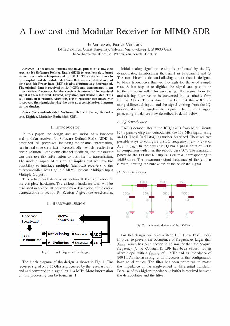
A Low-cost and Modular Receiver for MIMO SDR Jo Verhaevert, Patrick Van Torre INTEC-iMinds, Ghent University, Valentin Vaerwyckweg 1, B-9000 Gent, [email protected],[email protected] Abstract—This article outlines the development of a low-cost receiver for Software Defined Radio (SDR) to receive a data burst on an intermediate frequency of 113 MHz. This data will have to be sampled and demodulated. Constellations are plotted in real time and Bit Error Rate (BER) is also continuously determined. The original data is received on 2.45 GHz and transformed to an intermediate frequency by the receiver front-end. The received signal is then buffered, filtered, amplified and demodulated. This is all done in hardware. After this, the microcontroller takes over to process the signal, showing the data as a constellation diagram on the display. Index Terms—Embedded Software Defined Radio, Demodu- late, Digitize, Modular Embedded SDR. I. I NTRODUCTION In this paper, the design and realization of a low-cost and modular receiver for Software Defined Radio (SDR) is described. All processes, including the channel information, run in real-time on a fast microcontroller, which results in a cheap solution. Employing channel feedback, the transmitter can then use this information to optimize its transmission. The modular aspect of this design implies that we have the possibility to interface multiple (identical) receivers to the microcontroller, resulting in a MIMO-system (Multiple Input Multiple Output). This article will discuss in section II the realization of the complete hardware. The different hardware tests will be discussed in section III, followed by a description of the entire demodulation in section IV. Section V gives the conclusions. II. HARDWARE DESIGN Fig. 1. Block diagram of the design. The block diagram of the design is shown in Fig. 1. The received signal on 2.45 GHz is processed by the receiver front- end and converted to a signal on 113 MHz. More information on this processing can be found in [1]. Initial analog signal processing is performed by the IQ- demodulator, transforming the signal in baseband I and Q. The next block is the anti-aliasing circuit that is designed to block frequencies that are too high for the used sample rate. A last step is to digitize the signal and pass it on to the microcontroller for processing. The signal from the anti-aliasing filter has to be converted into a suitable form for the ADCs. This is due to the fact that the ADCs are using differential inputs and the signal coming from the IQ- demodulator is a single-ended signal. The different signal processing blocks are now described in detail below. A. IQ-demodulator The IQ-demodulator is the JCIQ-176D from Mini-Circuits [2], a passive chip that demodulates the 113 MHz signal using an LO (Local Oscillator), as further described. There are two possible ways to configure the LO frequency: f LO >f RF or f LO <f RF . In the first case, Q has a phase shift of -90 ◦ in comparison with I, in the second case 90 ◦ . The maximum power on the LO and RF inputs is 50 mW, corresponding to 16.99 dBm. The maximum output frequency of this chip is 5 MHz, limiting the bandwidth of the baseband signal. B. Low Pass Filter Fig. 2. Schematic diagram of the LC-Filter. For this design, we need a steep LPF (Low Pass Filter), in order to prevent the occurrence of frequencies larger than f max , which has been chosen to be smaller than the Nyquist frequency f s . A Constant-K LPF has been chosen for its sharp slope, with a f cutof f of 1 MHz and an impedance of 500 Ω. As shown in Fig. 2, all inductors in this configuration have equal values. The filter has been optimized to match the impedance of the single-ended to differential translator. Because of this higher impedance, a buffer is required between the demodulator and the filter.
Transcript of A Low-cost and Modular Receiver for MIMO SDR · A Low-cost and Modular Receiver for MIMO SDR ......
A Low-cost and Modular Receiver for MIMO SDR
Jo Verhaevert, Patrick Van Torre
INTEC-iMinds, Ghent University, Valentin Vaerwyckweg 1, B-9000 Gent,
[email protected], [email protected]
Abstract—This article outlines the development of a low-costreceiver for Software Defined Radio (SDR) to receive a data burston an intermediate frequency of 113 MHz. This data will have tobe sampled and demodulated. Constellations are plotted in realtime and Bit Error Rate (BER) is also continuously determined.The original data is received on 2.45 GHz and transformed to anintermediate frequency by the receiver front-end. The receivedsignal is then buffered, filtered, amplified and demodulated. Thisis all done in hardware. After this, the microcontroller takes overto process the signal, showing the data as a constellation diagramon the display.
Index Terms—Embedded Software Defined Radio, Demodu-
late, Digitize, Modular Embedded SDR.
I. INTRODUCTION
In this paper, the design and realization of a low-cost
and modular receiver for Software Defined Radio (SDR) is
described. All processes, including the channel information,
run in real-time on a fast microcontroller, which results in a
cheap solution. Employing channel feedback, the transmitter
can then use this information to optimize its transmission.
The modular aspect of this design implies that we have the
possibility to interface multiple (identical) receivers to the
microcontroller, resulting in a MIMO-system (Multiple Input
Multiple Output).
This article will discuss in section II the realization of
the complete hardware. The different hardware tests will be
discussed in section III, followed by a description of the entire
demodulation in section IV. Section V gives the conclusions.
II. HARDWARE DESIGN
Fig. 1. Block diagram of the design.
The block diagram of the design is shown in Fig. 1. The
received signal on 2.45 GHz is processed by the receiver front-
end and converted to a signal on 113 MHz. More information
on this processing can be found in [1].
Initial analog signal processing is performed by the IQ-
demodulator, transforming the signal in baseband I and Q.
The next block is the anti-aliasing circuit that is designed
to block frequencies that are too high for the used sample
rate. A last step is to digitize the signal and pass it on
to the microcontroller for processing. The signal from the
anti-aliasing filter has to be converted into a suitable form
for the ADCs. This is due to the fact that the ADCs are
using differential inputs and the signal coming from the IQ-
demodulator is a single-ended signal. The different signal
processing blocks are now described in detail below.
A. IQ-demodulator
The IQ-demodulator is the JCIQ-176D from Mini-Circuits
[2], a passive chip that demodulates the 113 MHz signal using
an LO (Local Oscillator), as further described. There are two
possible ways to configure the LO frequency: fLO > fRF or
fLO < fRF . In the first case, Q has a phase shift of −90
in comparison with I, in the second case 90. The maximum
power on the LO and RF inputs is 50 mW, corresponding to
16.99 dBm. The maximum output frequency of this chip is
5 MHz, limiting the bandwidth of the baseband signal.
B. Low Pass Filter
Fig. 2. Schematic diagram of the LC-Filter.
For this design, we need a steep LPF (Low Pass Filter),
in order to prevent the occurrence of frequencies larger than
fmax, which has been chosen to be smaller than the Nyquist
frequency fs. A Constant-K LPF has been chosen for its
sharp slope, with a fcutoff of 1 MHz and an impedance of
500 Ω. As shown in Fig. 2, all inductors in this configuration
have equal values. The filter has been optimized to match
the impedance of the single-ended to differential translator.
Because of this higher impedance, a buffer is required between
the demodulator and the filter.
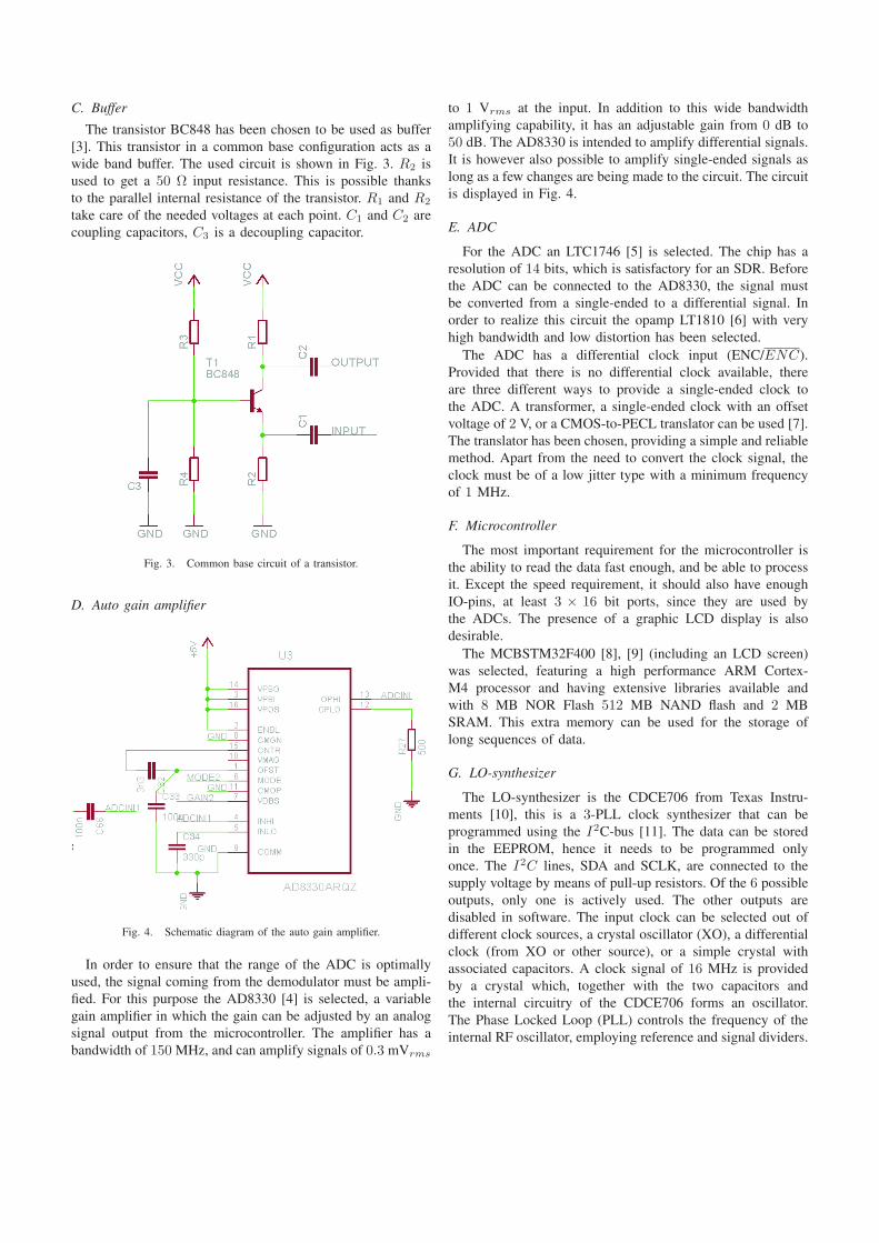
C. Buffer
The transistor BC848 has been chosen to be used as buffer
[3]. This transistor in a common base configuration acts as a
wide band buffer. The used circuit is shown in Fig. 3. R2 is
used to get a 50 Ω input resistance. This is possible thanks
to the parallel internal resistance of the transistor. R1 and R2
take care of the needed voltages at each point. C1 and C2 are
coupling capacitors, C3 is a decoupling capacitor.
Fig. 3. Common base circuit of a transistor.
D. Auto gain amplifier
Fig. 4. Schematic diagram of the auto gain amplifier.
In order to ensure that the range of the ADC is optimally
used, the signal coming from the demodulator must be ampli-
fied. For this purpose the AD8330 [4] is selected, a variable
gain amplifier in which the gain can be adjusted by an analog
signal output from the microcontroller. The amplifier has a
bandwidth of 150 MHz, and can amplify signals of 0.3 mVrms
to 1 Vrms at the input. In addition to this wide bandwidth
amplifying capability, it has an adjustable gain from 0 dB to
50 dB. The AD8330 is intended to amplify differential signals.
It is however also possible to amplify single-ended signals as
long as a few changes are being made to the circuit. The circuit
is displayed in Fig. 4.
E. ADC
For the ADC an LTC1746 [5] is selected. The chip has a
resolution of 14 bits, which is satisfactory for an SDR. Before
the ADC can be connected to the AD8330, the signal must
be converted from a single-ended to a differential signal. In
order to realize this circuit the opamp LT1810 [6] with very
high bandwidth and low distortion has been selected.
The ADC has a differential clock input (ENC/ENC).
Provided that there is no differential clock available, there
are three different ways to provide a single-ended clock to
the ADC. A transformer, a single-ended clock with an offset
voltage of 2 V, or a CMOS-to-PECL translator can be used [7].
The translator has been chosen, providing a simple and reliable
method. Apart from the need to convert the clock signal, the
clock must be of a low jitter type with a minimum frequency
of 1 MHz.
F. Microcontroller
The most important requirement for the microcontroller is
the ability to read the data fast enough, and be able to process
it. Except the speed requirement, it should also have enough
IO-pins, at least 3 × 16 bit ports, since they are used by
the ADCs. The presence of a graphic LCD display is also
desirable.
The MCBSTM32F400 [8], [9] (including an LCD screen)
was selected, featuring a high performance ARM Cortex-
M4 processor and having extensive libraries available and
with 8 MB NOR Flash 512 MB NAND flash and 2 MB
SRAM. This extra memory can be used for the storage of
long sequences of data.
G. LO-synthesizer
The LO-synthesizer is the CDCE706 from Texas Instru-
ments [10], this is a 3-PLL clock synthesizer that can be
programmed using the I2C-bus [11]. The data can be stored
in the EEPROM, hence it needs to be programmed only
once. The I2C lines, SDA and SCLK, are connected to the
supply voltage by means of pull-up resistors. Of the 6 possible
outputs, only one is actively used. The other outputs are
disabled in software. The input clock can be selected out of
different clock sources, a crystal oscillator (XO), a differential
clock (from XO or other source), or a simple crystal with
associated capacitors. A clock signal of 16 MHz is provided
by a crystal which, together with the two capacitors and
the internal circuitry of the CDCE706 forms an oscillator.
The Phase Locked Loop (PLL) controls the frequency of the
internal RF oscillator, employing reference and signal dividers.
III. HARDWARE TESTS
A. LO-synthesizer
Fig. 5 shows the harmonic frequencies of the synthesizer.
The first harmonic frequency (marker 2 in the figure) is
approximately 10 dB below the fundamental frequency. Fig.
6 shows the fundamental frequency of the synthesizer and the
spurious sidebands at least 44 dB below the carrier.
Fig. 5. Harmonic frequencies of LO-Synthesizer.
Fig. 6. 113 MHz center frequency.
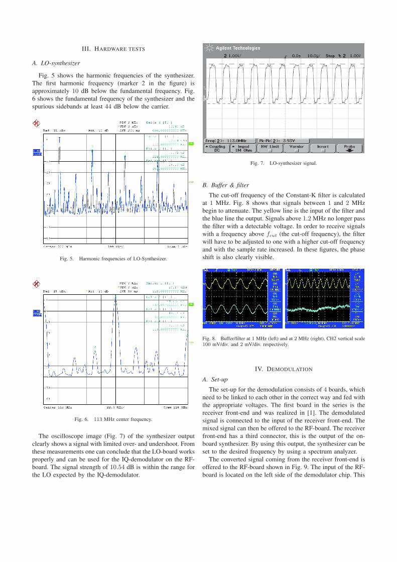
The oscilloscope image (Fig. 7) of the synthesizer output
clearly shows a signal with limited over- and undershoot. From
these measurements one can conclude that the LO-board works
properly and can be used for the IQ-demodulator on the RF-
board. The signal strength of 10.54 dB is within the range for
the LO expected by the IQ-demodulator.
Fig. 7. LO-synthesizer signal.
B. Buffer & filter
The cut-off frequency of the Constant-K filter is calculated
at 1 MHz. Fig. 8 shows that signals between 1 and 2 MHz
begin to attenuate. The yellow line is the input of the filter and
the blue line the output. Signals above 1.2 MHz no longer pass
the filter with a detectable voltage. In order to receive signals
with a frequency above fcut (the cut-off frequency), the filter
will have to be adjusted to one with a higher cut-off frequency
and with the sample rate increased. In these figures, the phase
shift is also clearly visible.
Fig. 8. Buffer/filter at 1 MHz (left) and at 2 MHz (right), CH2 vertical scale100 mV/div. and 2 mV/div. respectively.
IV. DEMODULATION
A. Set-up
The set-up for the demodulation consists of 4 boards, which
need to be linked to each other in the correct way and fed with
the appropriate voltages. The first board in the series is the
receiver front-end and was realized in [1]. The demodulated
signal is connected to the input of the receiver front-end. The
mixed signal can then be offered to the RF-board. The receiver
front-end has a third connector, this is the output of the on-
board synthesizer. By using this output, the synthesizer can be
set to the desired frequency by using a spectrum analyzer.
The converted signal coming from the receiver front-end is
offered to the RF-board shown in Fig. 9. The input of the RF-
board is located on the left side of the demodulator chip. This
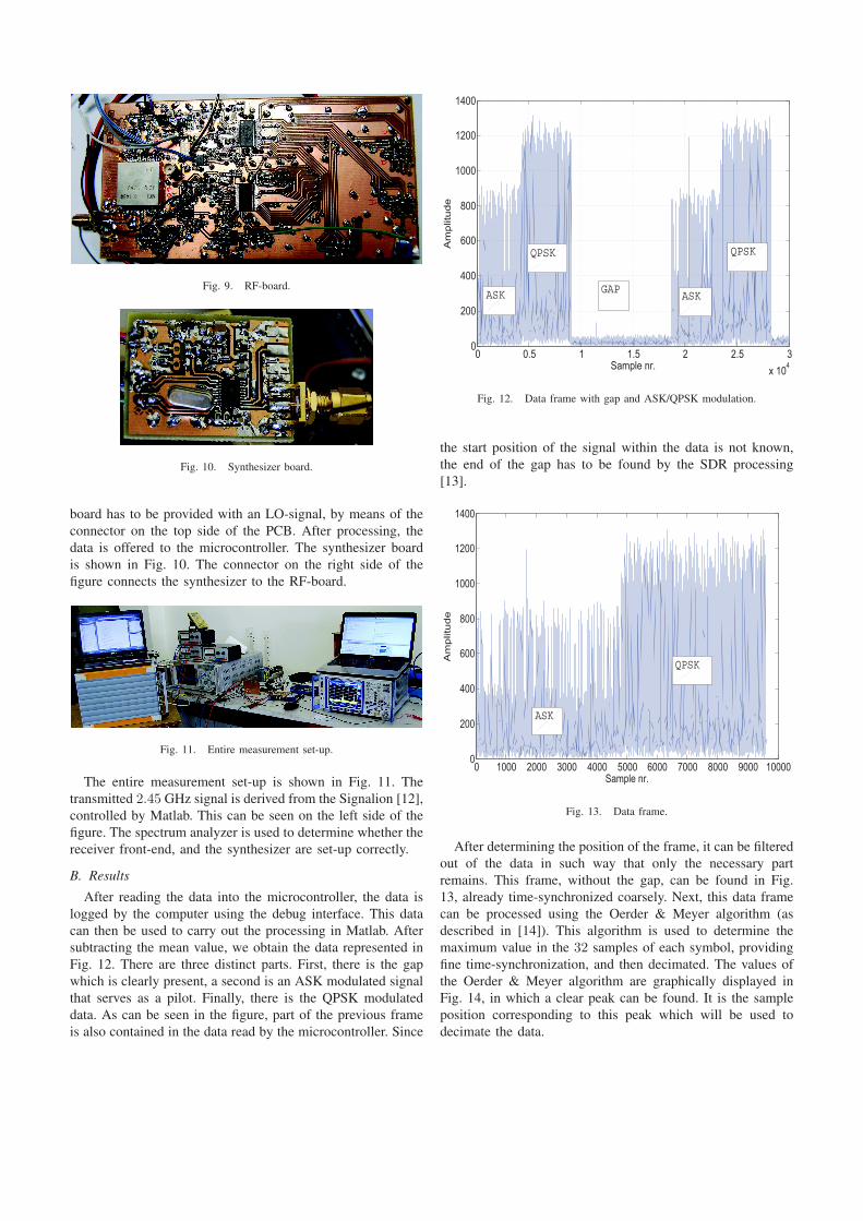
Fig. 9. RF-board.
Fig. 10. Synthesizer board.
board has to be provided with an LO-signal, by means of the
connector on the top side of the PCB. After processing, the
data is offered to the microcontroller. The synthesizer board
is shown in Fig. 10. The connector on the right side of the
figure connects the synthesizer to the RF-board.
Fig. 11. Entire measurement set-up.
The entire measurement set-up is shown in Fig. 11. The
transmitted 2.45 GHz signal is derived from the Signalion [12],
controlled by Matlab. This can be seen on the left side of the
figure. The spectrum analyzer is used to determine whether the
receiver front-end, and the synthesizer are set-up correctly.
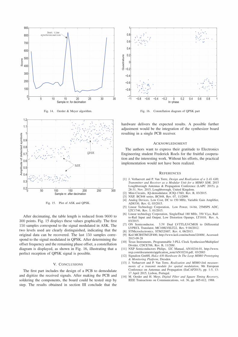
B. Results
After reading the data into the microcontroller, the data is
logged by the computer using the debug interface. This data
can then be used to carry out the processing in Matlab. After
subtracting the mean value, we obtain the data represented in
Fig. 12. There are three distinct parts. First, there is the gap
which is clearly present, a second is an ASK modulated signal
that serves as a pilot. Finally, there is the QPSK modulated
data. As can be seen in the figure, part of the previous frame
is also contained in the data read by the microcontroller. Since
0 0.5 1 1.5 2 2.5 3
x 104
0
200
400
600
800
1000
1200
1400
Sample nr.
Am
plitu
de
GAP
QPSK QPSK
ASKASK
Fig. 12. Data frame with gap and ASK/QPSK modulation.
the start position of the signal within the data is not known,
the end of the gap has to be found by the SDR processing
[13].
0 1000 2000 3000 4000 5000 6000 7000 8000 9000 100000
200
400
600
800
1000
1200
1400
Sample nr.
Am
plitu
de
QPSK
ASK
Fig. 13. Data frame.
After determining the position of the frame, it can be filtered
out of the data in such way that only the necessary part
remains. This frame, without the gap, can be found in Fig.
13, already time-synchronized coarsely. Next, this data frame
can be processed using the Oerder & Meyer algorithm (as
described in [14]). This algorithm is used to determine the
maximum value in the 32 samples of each symbol, providing
fine time-synchronization, and then decimated. The values of
the Oerder & Meyer algorithm are graphically displayed in
Fig. 14, in which a clear peak can be found. It is the sample
position corresponding to this peak which will be used to
decimate the data.
0 5 10 15 20 25 30 350
100
200
300
400
500
600
700
800
900
Sample nr. for decimation
Sco
re
Best time synchronisation
Fig. 14. Oerder & Meyer algorithm.
0 50 100 150 200 250 3000.2
0.3
0.4
0.5
0.6
0.7
0.8
0.9
1
1.1
1.2
Sample nr. after decimation
Am
plitu
de
of
de
tecte
d s
ym
bo
ls
QPSK
ASK
Fig. 15. Plot of ASK and QPSK.
After decimating, the table length is reduced from 9600 to
300 points. Fig. 15 displays these values graphically. The first
150 samples correspond to the signal modulated in ASK. The
two levels used are clearly distinguished, indicating that the
original data can be recovered. The last 150 samples corre-
spond to the signal modulated in QPSK. After determining the
offset frequency and the remaining phase offset, a constellation
diagram is displayed, as shown in Fig. 16, illustrating that a
perfect reception of QPSK signal is possible.
V. CONCLUSIONS
The first part includes the design of a PCB to demodulate
and digitize the received signals. After making the PCB and
soldering the components, the board could be tested step by
step. The results obtained in section III conclude that the
−1 −0.8 −0.6 −0.4 −0.2 0 0.2 0.4 0.6 0.8 1−1
−0.8
−0.6
−0.4
−0.2
0
0.2
0.4
0.6
0.8
1
In−phase
Qu
ad
ratu
re
Fig. 16. Constellation diagram of QPSK part
hardware delivers the expected results. A possible further
adjustment would be the integration of the synthesizer board
resulting in a single PCB receiver.
ACKNOWLEDGMENT
The authors want to express their gratitude to Electronics
Engineering student Frederick Roels for the fruitful coopera-
tion and the interesting work. Without his efforts, the practical
implementation would not have been realized.
REFERENCES
[1] J. Verhaevert and P. Van Torre, Design and Realization of a 2.45 GHz
Transmitter and Receiver as a Modular Unit for a MIMO SDR, 2015Loughborough Antennas & Propagation Conference (LAPC 2015), p.28-31, Nov. 2015, Loughborough, United Kingdom.
[2] Mini-Circuits, IQ-demodulator, JCIQ-176D, Rev. B, 03/2015.[3] NXP, BC848 series, BC848, Rev. 07, 11/2009.[4] Analog Devices, Low Cost, DC to 150 MHz, Variable Gain Amplifier,
AD8330, Rev. G, 03/2015.[5] Linear Technology Corporation, Low Power, 14-bit, 25MSPS ADC,
LTC1746, Rev. 3, 01/2015.[6] Linear technology Corporation, Single/Dual 180 MHz, 350 V/µs, Rail-
to-Rail Input and Output, Low Distortion Opamps, LT1810, Rev. A,03/2015.
[7] ON Semiconductor, 3.3V Dual LVTTL/LVCMOS to DifferentialLVPECL Translator, MC100LVELT22, Rev. 9 04/2012.
[8] STMicroelectronics, STM32f407, Rev. 4, 06/2013.[9] Keil MCBSTM32F400, http://www.keil.com/mcbstm32f400/, Accessed:
2015-09-28[10] Texas Instruments, Programmable 3-PLL Clock Synthesizer/Multiplier/
Divider, CDCE706, Rev. B, 11/200/.[11] NXP Semiconductors Philips, I2C Manual, AN10216-01, http://www.
nxp.com/documents/application note/AN10216.pdf, 03/2003[12] Signalion GmbH, HaLo 430 Hardware In The Loop MIMO Prototyping
& Monitoring Platform, Dresden.[13] J. Verhaevert and P. Van Torre, Realization and MIMO-link measure-
ments of a transmit module for spatial modulation, 9th EuropeanConference on Antennas and Propagation (EuCAP2015), pp. 1-5, 13-17 April 2015, Lisbon, Portugal.
[14] M. Oerder and H. Meyr, Digital Filter and Square Timing Recovery,IEEE Transactions on Communications, vol. 36, pp. 605-612, 1988.