Silicon Photonics: an Industrial Perspective -...
32
Silicon Photonics: an Industrial Perspective Antonio Fincato Advanced Programs R&D, Cornaredo, Italy
Transcript of Silicon Photonics: an Industrial Perspective -...

Silicon Photonics:
an Industrial Perspective
Antonio Fincato
Advanced Programs R&D, Cornaredo, Italy

OUTLINE 2
A. Fincato - Silicon Photonics: an Industrial Perspective 27/10/2016
• Introduction
• Silicon Photonics Concept
• 300mm (12’’) Photonic Process
• Main Silicon Photonics Devices
• Future Evolution
• Conclusion

OUTLINE 3
A. Fincato - Silicon Photonics: an Industrial Perspective 27/10/2016
• Introduction
• Silicon Photonics Concept
• 300mm (12’’) Photonic Process
• Main Silicon Photonics Devices
• Future Evolution
• Conclusion

Silicon Photonics Main Application Areas 4
A. Fincato - Silicon Photonics: an Industrial Perspective 27/10/2016
High Performance Computer Data Center Access Network
Typical Losses of Electrical
Transmission Lines @ 15GHz
RF Cable 1dB/m
Backplane 3 dB/cm
Board 1 dB/cm
Intrachip 1 dB/mm
Typical Losses of Optical Transmission
Lines @ 1310nm
SM Fiber 0.5 dB/km
Si waveguide 0.2-2 dB/cm
SiN waveguide 0.1dB/cm
SiO2 waveguide < 0.1 dB/cm

The Zettabyte Era
• By the end of 2016, global IP traffic will
reach 1.1 ZB per year, or 88.7 EB per
month
• By 2020 global IP traffic will reach 2.3
ZB per year, or 194 EB per month
• Overall, IP traffic will grow at a
compound annual growth rate (CAGR)
of 22% from 2015 to 2020
5
The Zettabyte Era: Trends and Analysis, July 2016 - White Paper - CISCO
http://www.cisco.com/c/en/us/solutions/collateral/service-provider/visual-networking-index-vni/vni-hyperconnectivity-wp.html
A. Fincato - Silicon Photonics: an Industrial Perspective 27/10/2016

Global Data Center IP Traffic:
Three-Fold Increase by 2019 • Annual global data center IP traffic will
reach 10.4 ZB (863 EB per month) by
the end of 2019, up from 3.4 ZB per year
(287 EB per month) in 2014.
• Global data center IP traffic will grow 3-
fold over the next 5 years. Overall, data
center IP traffic will grow at a compound
annual growth rate (CAGR) of 25% from
2014 to 2019.
• By 2019, 86% of workloads will be
processed by cloud data centers; 14%
will be processed by traditional data
centers.
6
Cisco Global Cloud Index: Forecast and Methodology, 2014–2019 - White Paper - CISCO
http://www.cisco.com/c/en/us/solutions/collateral/service-provider/global-cloud-index-gci/Cloud_Index_White_Paper.pdf
A. Fincato - Silicon Photonics: an Industrial Perspective 27/10/2016
Zettabyte per Year

Supercomputing Power Growth
• Exponential growth of
supercomputing power as recorded
by the TOP500 list
7
TOP 500
https://www.top500.org/statistics/perfdevel/
A. Fincato - Silicon Photonics: an Industrial Perspective 27/10/2016

8
A. Fincato - Silicon Photonics: an Industrial Perspective 27/10/2016
International Standard Requests
Speed will increase Size and power will decrease
http://www.ethernetalliance.org/roadmap/

OUTLINE 9
A. Fincato - Silicon Photonics: an Industrial Perspective 27/10/2016
• Introduction
• Silicon Photonics Concept
• 300mm (12’’) Photonic Process
• Main Silicon Photonics Devices
• Future Evolution
• ConclusionTotal internal reflection is a special optical
condition in which optical rays cannot escape
the material in which they are traveling.
John Tyndall

Optical Properties of Silicon in Near IR (1) 10
A. Fincato - Silicon Photonics: an Industrial Perspective 27/10/2016
Indirect Bandgap
No laser source
Centro-Symmetric Crystal
No Electrooptic effect
Momentum
not conserved

Optical Properties of Silicon in Near IR (2) 11
A. Fincato - Silicon Photonics: an Industrial Perspective 27/10/2016
Wavelength (nm)
VISIBLE
Photodetectors
Transparency
Wavelength (nm)
Ab
so
rptio
n c
oe
ffic
ient (c
m-1
)
Silicon Absorption Coefficient

Electronic-Photonic Monolitic Integration (1)
Samsung, OFC 2013IBM, IEDM 2012Luxtera, ISSCC 2006
<100nm
0.1 µm 0.02 µm
<10nm
1 µm
BO
XS
OI
200-500nm
Photonics PD-SOI or SOI-FinFET UTBB-FDSOI Bulk
28nm,14nm,10nm 55nm, 28nm,20nm22,14,10 nm FinFET
SOI 130nm,90nm,45nm
BUT
12
A. Fincato - Silicon Photonics: an Industrial Perspective 27/10/2016
CMOS 130nm CMOS 90nm DRAM

13
Photonics Electronics
Local Photonics Substrate creation
Samsung, OFC 2013,GFP2013Micron, VLSI tech. 2014IHP, GFP 2013
Photonics Electronics
Integrate CMOS on Photonics Substrate
Luxtera, ISSCC 2006,IBM, IEDM 2012
Need a re-development of the CMOS technology Cost issues , especially with Advanced
Technologies (55nm and below)
Electronic-Photonic Monolitic Integration (2)
A. Fincato - Silicon Photonics: an Industrial Perspective 27/10/2016

143D Integration Strategy of ST
A. Fincato - Silicon Photonics: an Industrial Perspective 27/10/2016
Opto-Electronic System = Photonic IC + Electronic IC
Opto-Electronic IC
Electronic IC:CMOS or BiCMOS
Cu pillar
Independent evolution for optimization of technology platform
(process flow & design environment)Opto-Electronic
System
Photonic IC
Cu pillar

15
EIC PIC
EIC
PIC
40µmPIC
EIC
3D integration: F2F Assembly
A. Fincato - Silicon Photonics: an Industrial Perspective 27/10/2016

OUTLINE 16
A. Fincato - Silicon Photonics: an Industrial Perspective 27/10/2016
• Introduction
• Silicon Photonics Concept
• 300mm (12’’) Photonic Process
• Main Silicon Photonics Devices
• Future Evolution
• Conclusion

PIC25G Silicon Photonics Technology Platform 17
A. Fincato - Silicon Photonics: an Industrial Perspective 27/10/2016
Joint Development started 2012
l Type Function
l=1
31
0n
m &
14
90
nm
Optical Passives
Multimode waveguide
Single Mode waveguide
Curved waveguide
Tapered waveguide
90°C Bend (R=40µm)
Directional coupler – Split ratio 1÷99%
Y-junction: Splitter
Fiber (8°) Single Polarization Grating Coupler (TX-out)
Laser (13.2°) Single Polarization Grating Coupler (TX-in)
Dual Polarization Grating Coupler (RX-in)
WG termination
Optical ModulatorsHigh Speed Amplitude Modulator – Vcc=1.8V-2.5V
Phase Modulator – Vcc = 2.5V
Photodiode High Speed PiN PD - Vcc=1.0 ÷ 1.6V

ST Silicon Photonics Platform: PIC25G 18
Back End of Layer stack cross section
Single Mode Waveguide cross-section
A. Fincato - Silicon Photonics: an Industrial Perspective 27/10/2016
F.Boeuf et al., Electron Devices Meeting (IEDM),
2013 IEEE International , 9-11 Dec. 2013

300mm PhotonicsTool Set Portfolio
300mm PHOTONICS Technological Platform
300mm Process Integration 19
Etch
SiGe & Ge epitaxies
193 nm Litho
Low T° DepNi,Co,Pt silicide
193 i
Existing Tools
High volume
Sub-90nm CMOS node tools
193nm/193i photolithography
Improved Process control
A. Fincato - Silicon Photonics: an Industrial Perspective 27/10/2016

Silicon Photonics pros and cons
• Key driving force
• Fabrication based on CMOS technology
High volume production
Low cost [ $/Gbps ]
Small size [ mm3/Gbps ]
• Scalability
Speed
Channel number
Wavelength number
Number of functions
Different kind of modulation
20
• Drawbacks:
• Silicon is an indirect bandgap material
Very inefficient light emitter
• Si Photodetectors not available at
1310nm and 1550nm Telecom
wavelength
• Light modulation or amplification not
possible using direct properties of Silicon
A. Fincato - Silicon Photonics: an Industrial Perspective 27/10/2016
Made possible by CMOS technology
It is possible to overcome those difficulties by means of:
• Monolithic or Hybrid Integration
of different materials
• Dedicated architectures
BUT

OUTLINE 21
A. Fincato - Silicon Photonics: an Industrial Perspective 27/10/2016
• Introduction
• Silicon Photonics Concept
• 300mm (12’’) Photonic Process
• Main Silicon Photonics Devices
• Future Evolution
• Conclusion
Photodiode PhaseModulator SPGC PSGC DC WG

Fiber coupling 22
• Mode mismatch:
• Size 10mm vs 400nm
Spot-size converter
• Polarization problem:
• Only TE mode is propagatedin Si-waveguide
Polarization splitter AND
polarization rotator
10mm
Single-mode Fiber Optical Core
Silicon waveguide
A. Fincato - Silicon Photonics: an Industrial Perspective 27/10/2016
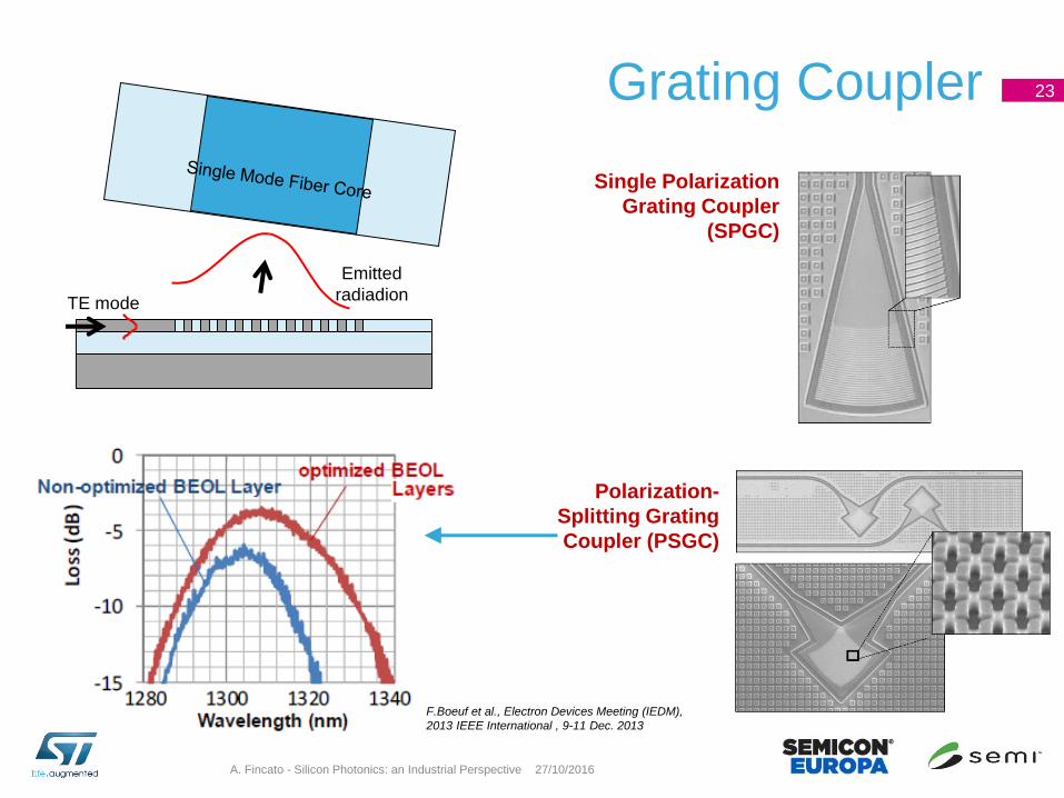
Grating Coupler 23
Single Polarization
Grating Coupler
(SPGC)
Polarization-
Splitting Grating
Coupler (PSGC)
A. Fincato - Silicon Photonics: an Industrial Perspective 27/10/2016
TE mode
Emitted
radiadion
F.Boeuf et al., Electron Devices Meeting (IEDM),
2013 IEEE International , 9-11 Dec. 2013

Carrier Depletion 24
Lightly doped p- and n- regions are realized in the
waveguide to form a p–n diode. The depletion
area of the diode becomes larger with increasing
reverse bias voltage.
PN
PNnnn
he
he
1818
8.01822
100.6105.8
105.8108.8
Real refractive index and absorption coefficient of the
doped Si regions due to the free-carrier dispersion
(R. A. Soref and B. R. Bennett - 1986):
where:
Δne is the refractive index change due to electron
concentration change
Δnh is the refractive index change due to hole
concentration change
ΔN is the electron concentration change in cm-3
ΔP is the hole concentration change in cm-3
Δe (in cm-1) is the absorption coefficient variations
due to ΔN
Δh (in cm-1) is the absorption coefficient variation
due to ΔP
losses of 0.1 dB/cm require ΔN < 2.7x10¹⁵
cm–3 or ΔP < 3.8x1015 cm–3 material
A. Fincato - Silicon Photonics: an Industrial Perspective 27/10/2016

Carrier Depletion Based High-Speed Phase Modulator25
M1
M2
Single mode waveguide
np
Insertion loss vs Phase Shift vs VoltageCut-off frequency measurement
A. Fincato - Silicon Photonics: an Industrial Perspective 27/10/2016

Mach-Zehnder Interferometer Modulator
0
0.5
1
0.00 0.39 0.79 1.18 1.57
Pcross
Pbar
26
LnP
LnP
gbar
gcross
0
2
0
2
sin
cos
l
l
A. Fincato - Silicon Photonics: an Industrial Perspective 27/10/2016

Germanium Photodetector 27
TEM Cross Section
Top view
Ge PiN diode I-V curve(λ=1310nm) Ge PD 3dB Modulation Bandwidth
A. Fincato - Silicon Photonics: an Industrial Perspective 27/10/2016
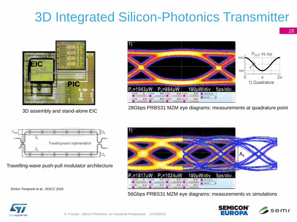
3D Integrated Silicon-Photonics Transmitter28
EIC
PIC
A. Fincato - Silicon Photonics: an Industrial Perspective 27/10/2016
Travelling-wave push-pull modulator architecture
56Gbps PRBS31 MZM eye diagrams: measurements vs simulations
28Gbps PRBS31 MZM eye diagrams: measurements at quadrature point3D assembly and stand-alone EIC
Enrico Temporiti et al., ISSCC 2016

Test Interface:• DC/RF Probes• Optical head with a 16-channel Fiber
Array mounted on 6 axis micro positioner• Use of a capacitive sensor to fine adjust
distance from wafer top
300mm Photonics Testing29
Enable full auto characterization at wafer /lot scale (300mm) of:• All Optical passive devices (Waveguide /
coupler / MZI…)• Electro Optical devices: (photodiode /
modulator…)• Modulation Bandwidth up to 67GHz• BER & Eye Diagram up to 28Gbs/s
Mea
s. C
on
tro
l
Op
tica
l / R
F /
DC
Mea
s.
Fu
ll A
uto
Pro
be
r.
Test Interface
Auto alignement of the fiber array on the grating
coupler & fine positioning with piezoelectric
actuators X
Y
Optical power
A. Fincato - Silicon Photonics: an Industrial Perspective 27/10/2016

OUTLINE 30
A. Fincato - Silicon Photonics: an Industrial Perspective 27/10/2016
• Introduction
• Silicon Photonics Concept
• 300mm (12’’) Photonic Process
• Main Silicon Photonics Devices
• Future Evolution
• Conclusion
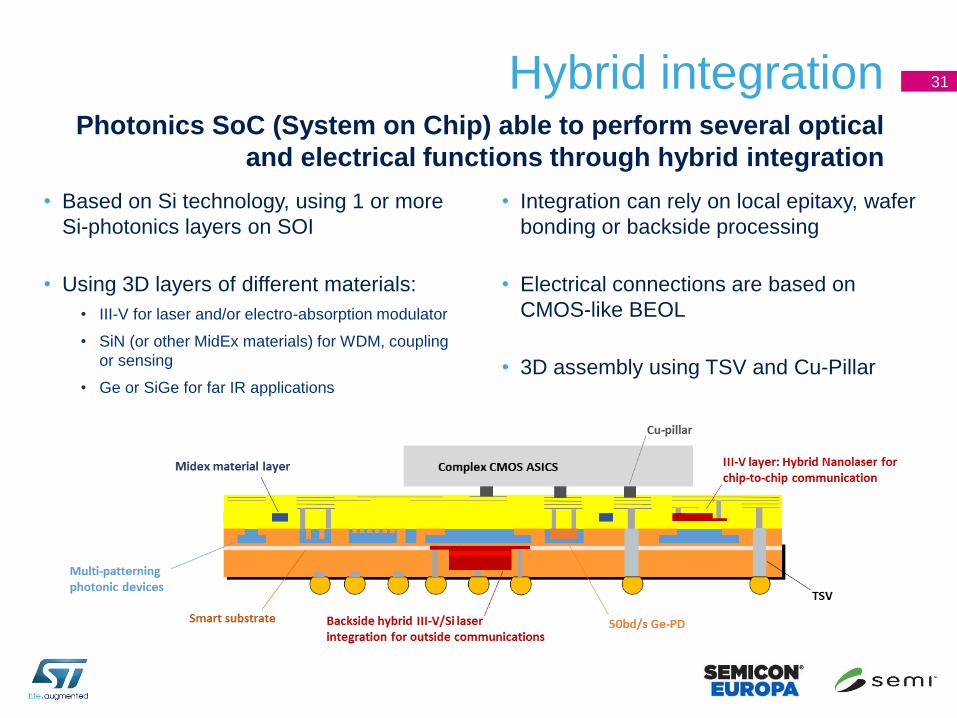
Hybrid integration 31
• Based on Si technology, using 1 or more
Si-photonics layers on SOI
• Using 3D layers of different materials:
• III-V for laser and/or electro-absorption modulator
• SiN (or other MidEx materials) for WDM, coupling
or sensing
• Ge or SiGe for far IR applications
• Integration can rely on local epitaxy, wafer
bonding or backside processing
• Electrical connections are based on
CMOS-like BEOL
• 3D assembly using TSV and Cu-Pillar
Photonics SoC (System on Chip) able to perform several optical
and electrical functions through hybrid integration

Conclusions 32
A. Fincato - Silicon Photonics: an Industrial Perspective 27/10/2016
• After 25 years of research Silicon Photonics has now reached an
industrial maturity for mass production
• Data-center market will be the main driver for the next 5 years
• Scalability, cost reduction and downsizing are key factors making
Silicon Photonics the only technology allowing to address the
requirements of future products for high speed communications
• 3D face-to-face assembly of PIC and EIC allows maximum flexibility
of both photonic and electronic processes
• Photonics on Silicon substrate has the potential to increase his
capabilities thanks to the numerous integration opportunities of
different materials