S3F8S5A Development Kit User Manual
24
S3 Family of Microcontrollers S3F8S5A Development Kit Copyright ©2016 Zilog ® , Inc. All rights reserved. www.zilog.com UM027202-0816 User Manual
Transcript of S3F8S5A Development Kit User Manual

S3 Family of Microcontrollers
S3F8S5A Development Kit
Copyright ©2016 Zilog®, Inc. All rights reserved.www.zilog.com
UM027202-0816
User Manual

S3F8S5A Development KitUser Manual
ii
DO NOT USE THIS PRODUCT IN LIFE SUPPORT SYSTEMS.
LIFE SUPPORT POLICYZILOG’S PRODUCTS ARE NOT AUTHORIZED FOR USE AS CRITICAL COMPONENTS IN LIFE SUPPORT DEVICES OR SYSTEMS WITHOUT THE EXPRESS PRIOR WRITTEN APPROVAL OF THE PRESIDENT AND GENERAL COUNSEL OF ZILOG CORPORATION.
As used hereinLife support devices or systems are devices which (a) are intended for surgical implant into the body, or (b) support or sustain life and whose failure to perform when properly used in accordance with instructions for use provided in the labeling can be reasonably expected to result in a significant injury to the user. A criti-cal component is any component in a life support device or system whose failure to perform can be reason-ably expected to cause the failure of the life support device or system or to affect its safety or effectiveness.
Document Disclaimer©2016 Zilog, Inc. All rights reserved. Information in this publication concerning the devices, applications, or technology described is intended to suggest possible uses and may be superseded. ZILOG, INC. DOES NOT ASSUME LIABILITY FOR OR PROVIDE A REPRESENTATION OF ACCURACY OF THE INFORMATION, DEVICES, OR TECHNOLOGY DESCRIBED IN THIS DOCUMENT. ZILOG ALSO DOES NOT ASSUME LIABILITY FOR INTELLECTUAL PROPERTY INFRINGEMENT RELATED IN ANY MANNER TO USE OF INFORMATION, DEVICES, OR TECHNOLOGY DESCRIBED HEREIN OR OTHERWISE. The information contained within this document has been verified according to the general principles of electrical and mechanical engineering.
S3 and Z8 are trademarks or registered trademarks of Zilog, Inc. All other product or service names are the property of their respective owners.
Warning:
UM027202-0816 Disclaimer

S3F8S5A Development KitUser Manual
iii
Revision HistoryEach instance in this document’s revision history reflects a change from its previous edi-tion. To learn more, refer to the corresponding page(s) or appropriate links furnished in the table below.
DateRevision Level Description Page
Aug 2016
02 Updated for ZDS-S3 version 5.3.0. Removed ISP I support
All
Jul 2015
01 Original issue. n/a
UM027202-0816 Revision History

S3F8S5A Development KitUser Manual
1
OverviewZilog’s S3F8S5A Development Kit, part number S3F8S5A0100ZCOG, allows you to evaluate your S3F8S5A-based designs and applications. The Kit features a Development Board consisting of the following components:
• Four LEDs
• Two pushbuttons
• Buzzer/Speaker
• LCD module
• UART
• 256 byte Serial EEPROM
• Header pins
This user manual provides instructions for setting up and configuring the S3F8S5A Devel-opment Board. It includes schematic diagrams and a discussion of the Board features and ZDS II.
The S3F8S5A Development Board features an S3F8S5A MCU in a 44-pin QFP package, plus an S3 PGM connector to connect the Board to a host development PC using the S3 Flash In-System Programmer II (ISP). To learn more about the S3F8S5A MCU, refer to the S3F8S5A Product Specification (PS0323) and/or the S3 Flash In-System Programmer User Manual (UM0266).
This document guides you through the following tasks:
• Downloading and installing ZDS II software and documentation
• Connecting the S3 Flash ISP II and S3F8S5A Development Board to your PC
• Starting the S3F8S5A Ledblink sample program
Kit ContentsThe S3F8S5A Development Kit contains the following items:
• S3F8S5A Development Board
• S3 Flash ISP II
• 10-circuit ribbon cable
• USB A (male) to Mini-B USB cable (2)
• S3F8S5A Development Kit hardcopy insert
UM027202-0816 Overview

S3F8S5A Development KitUser Manual
2
Figure 1 shows the contents of the S3F8S5A Development Kit.
FeaturesThe S3F8S5A Development Kit includes the following key items.
• S3F8S5A Development Board, which contains the following features:– S3F8S5A 44-pin QFP MCU operating at 12 MHz, with 48KB of internal Flash
memory and 1 KB of internal RAM memory – USB interface to supply power to the board– LCD module– Buzzer/Speaker– UART header at J8– 256 byte Serial EEPROM– Test Points headers for all pins of MCU– MCU current measurement Test Points J4 and J5– Pin P03/AD3 level adjustable with potentiometer R4
• S3 Flash In-System Programmer II
• ZDS II software, samples, and documentation available free for download– Sample programs
Figure 1. The S3F8S5A Development Kit
UM027202-0816 Features

S3F8S5A Development KitUser Manual
3
Supported Host EnvironmentsThe S3F8S5A Development Board supports the following operating systems:
• Microsoft Windows 7 (32-bit/64-bit)
• Microsoft Windows 8 (32-bit/64-bit)
Install the ZDS II Software and DocumentationObserve the following steps to download and install your ZDS II software and documenta-tion.
If you have already installed ZDS II – S3 <version> and have downloaded the software and documentation by following the procedure on the paper insert in your kit (FL0170), skip ahead to the next section.
1. Prior to connecting the S3F8S5A Development Board to your development PC, down-load ZDS II for S3 v5.3.0 (or later) from the Downloadable Software category in the Zilog Store.
2. When the download is complete, unzip the file to your hard drive, then double-click the installation file named ZDS2_S3_<Version>.exe and follow the on-screen instructions.
3. When the ZDS II installation is complete, double-click the installation file named DOCS_S3<version>.exe and follow the on-screen instructions.
4. When these installations are complete, view the S3F8S5A Development Kit User Manual (UM0272); this document will be located in the following path, by default: C:\Zilog\ZDSII_ S3 _<version>\Documentation\Tools_Documentation
Establish a Connection with the PCObserve the following procedure to connect the S3 Flash ISP II and S3F8S5A Develop-ment Board to your PC.
Note:
UM027202-0816 Supported Host Environments

S3F8S5A Development KitUser Manual
4
Disconnect or turn off the power to the S3F8S5A Development Board before connecting or disconnecting the S3 Flash ISP II.
1. Connect the Mini-B side of the USB A (male)-to-Mini-B cable to the S3 Flash ISP II. Connect the other end of this cable to the PC, as shown in Figure 2.
2. Connect the 10p 5x2 ribbon cable to the S3 Flash ISP II, as shown in Figure 3.
3. Connect the other end of the ribbon cable to Debug Connector J1 on the Development Board, shown in Figure 4.
Figure 2. Connecting the S3 Flash ISP II to the Development PC
Figure 3. Connecting the 10-pin Ribbon Cable to the S3 Flash ISP II
Caution:
UM027202-0816 Establish a Connection with the PC

S3F8S5A Development KitUser Manual
5
4. After completing the procedure to connect the S3F8S5A Development Board to the PC, the complete setup appears as shown in Figure 5.
Figure 4. Debug Connector J1
Figure 5. The Completed ISP II and Development Board Assembly
UM027202-0816 Establish a Connection with the PC
S3F8S5A Development KitUser Manual
6
Start the S3F8S5A Ledblink Sample ProgramThe S3F8S5A Development Kit includes a sample program that demonstrates an LED blinking application. To start the S3F8S5A Ledblink sample program, observe the follow-ing procedure.
1. Launch ZDS II by navigating from the Windows Start menu to Programs → Zilog ZDS II – S3 <Version> → ZDS II – S3 <Version>.
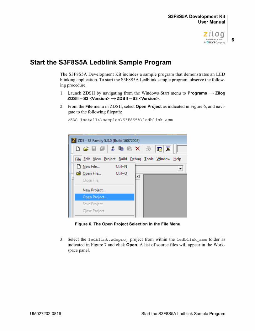
2. From the File menu in ZDS II, select Open Project as indicated in Figure 6, and navi-gate to the following filepath:
<ZDS Install>\samples\S3F8S5A\ledblink_asm
3. Select the ledblink.zdsproj project from within the ledblink_asm folder as indicated in Figure 7 and click Open. A list of source files will appear in the Work-space panel.
Figure 6. The Open Project Selection in the File Menu
UM027202-0816 Start the S3F8S5A Ledblink Sample Program

S3F8S5A Development KitUser Manual
7
4. From the Build menu, select Set Active Configuration to open the Select Configura-tion dialog box.
5. Select Debug, then click OK to close the Select Configuration dialog box.
6. From the Project menu in ZDS II, select Settings to open the Project Settings dialog box. In the Project Settings dialog box, click the Debugger tab.
Figure 7. Select the ledblink.zdsproj Project
UM027202-0816 Start the S3F8S5A Ledblink Sample Program

S3F8S5A Development KitUser Manual
8
7. On the Debugger page, select S3F8S5X_FlashIspII from the Target list, then select S3FlashIspII from the Debug Tool drop-down menu, as indicated in Figure 8.
8. After selecting S3FlashIspII from the Debug Tool drop-down menu, click Setup to select the serial number of the S3 Flash ISP II you are using, as indicated in Figure 9. Click OK to close the Setup USB Communication dialog box.
Figure 8. Select the Target and Debug Tool
UM027202-0816 Start the S3F8S5A Ledblink Sample Program

S3F8S5A Development KitUser Manual
9
The serial number you see on your screen will be different from the serial number shown in Figure 9.
9. After selecting the serial number of the S3 Flash ISP II that you are using, select Setup from the Target field to select the Target Voltage.
10. From the target Configuration dialog, enter “0” on ISP_DBRG_IDX and select the 3.3V by ISP button and Click OK. See Figure 10.
Figure 9. The Setup USB Communication Dialog
Note:
UM027202-0816 Start the S3F8S5A Ledblink Sample Program

S3F8S5A Development KitUser Manual
10
11. Make sure that the Enhanced ISP Debug Library is selected on the debugger win-dow..
12. Click OK to close the Project Settings dialog box.
13. If you are prompted to rebuild any affected files, click Yes. Otherwise, choose Buildfrom the menu bar, then click Rebuild All. The following example message is dis-played:
OUTPUT CHECKSUM
ledblink.hex F834 ledblink.lod F834
0 warning(s 0 error(s) Build succeeded.
Figure 10. The Target Configuration Dialog
Space Base Top Size Used UnusedPage0 P:00 P:05 COH 6H BAH
( 192 6 186 )ROM C:0000 C:1BB7 C000H 1AB8H A548H
( 49152 6840 42312 )
UM027202-0816 Start the S3F8S5A Ledblink Sample Program
S3F8S5A Development KitUser Manual
11
This Output Checksum message is an example and may not match the actual checksum of the project for a particular release of the ZDS installation software.
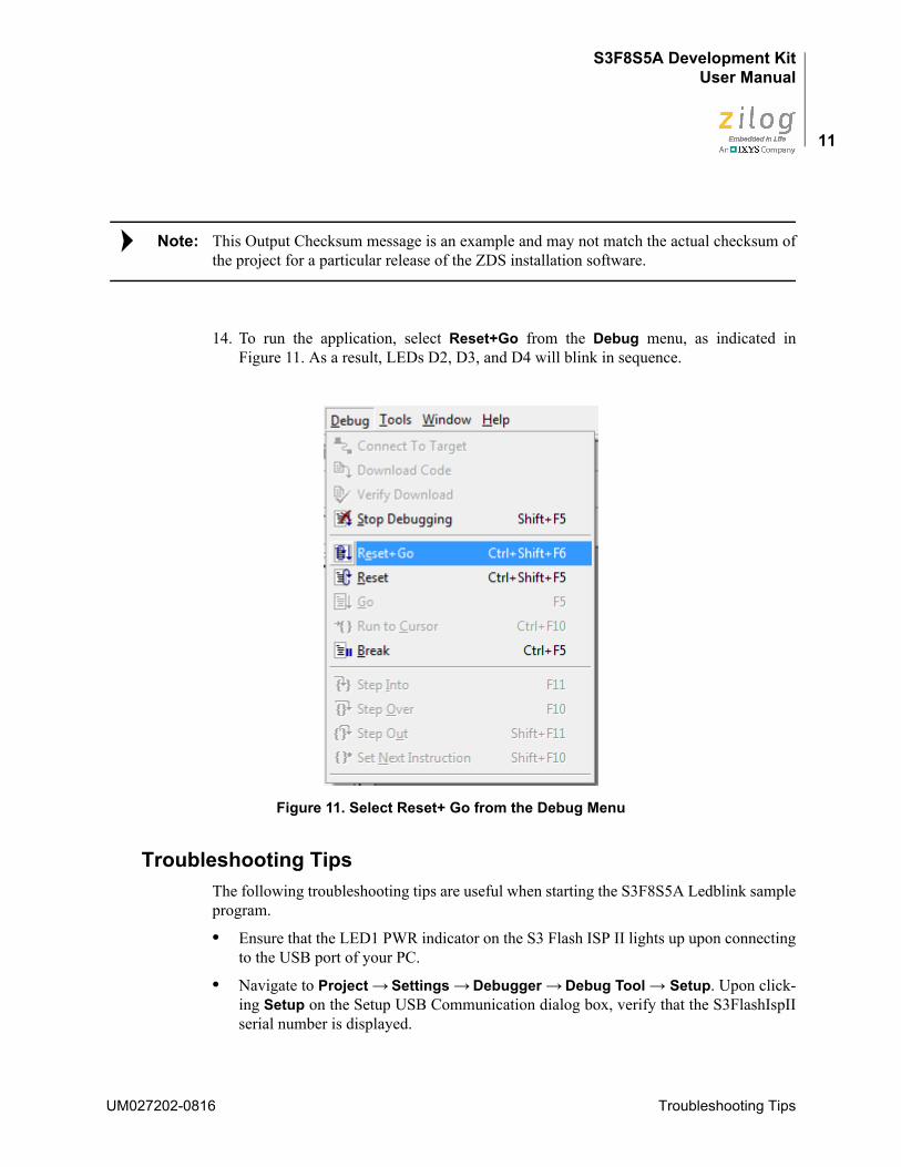
14. To run the application, select Reset+Go from the Debug menu, as indicated in Figure 11. As a result, LEDs D2, D3, and D4 will blink in sequence.
Troubleshooting TipsThe following troubleshooting tips are useful when starting the S3F8S5A Ledblink sample program.
• Ensure that the LED1 PWR indicator on the S3 Flash ISP II lights up upon connecting to the USB port of your PC.
• Navigate to Project → Settings → Debugger → Debug Tool → Setup. Upon click-ing Setup on the Setup USB Communication dialog box, verify that the S3FlashIspII serial number is displayed.
Figure 11. Select Reset+ Go from the Debug Menu
Note:
UM027202-0816 Troubleshooting Tips

S3F8S5A Development KitUser Manual
12
• Remove and reconnect the ISP II on the USB port of your PC.
• Refer to Figure 14 on page 13 to learn more about the operations and power options of the S3F8S5A Development Board.
S3F8S5A Development BoardThe purpose of the S3F8S5A Development Kit is to provide a set of hardware and soft-ware tools for the development of hardware and firmware for applications based on the S3F8S5A microcontroller. An image of the S3F8S5A Development Board is shown in Figure 12; a block diagram is shown in Figure 13.
Figure 12. The S3F8S5A Development Board
UM027202-0816 S3F8S5A Development Board

S3F8S5A Development KitUser Manual
13
Operations and Power OptionsThe operations and power options of the S3F8S5A Development Board are listed in Fig-ure 14.
Figure 13. S3F8S5A Development Board Block Diagram
Figure 14. Operations and Power Options of the S3F8S5A Development Board
UM027202-0816 Operations and Power Options

S3F8S5A Development KitUser Manual
14
S3F8S5A MCUKey features of the S3F8S5A MCU include:
• SAM88RC CPU core
• 48K x 8 bits program memory
• 1024 × 8 bits data memory
• Endurance: 10,000 Erase/Program cycles
• 78 instructions
• 36 normal I/O pins in the 44-pin QFP package
• Eight bit-programmable pins for external interrupts
• One 8-bit basic timer for oscillation stabilization and watchdog functions (system reset)
• Three 8-bit timer/counters and two 16-bit timer/counters with selectable operating modes
• Watch timer for real time
• LCD controller/driver
• A/D converter with 8 selectable input pins
• Synchronous SIO modules
• Two asynchronous UART modules
• Pattern generation module
To learn more about the S3F8S5A MCU, refer to the S3F8S5A Product Specification (PS0323).
Magnetic BuzzerThe CEM1206S magnetic buzzer (U5) manufactured by CUI Inc. is rated at a frequency of 2400 Hz and an operating voltage of 3.0–8.0 V zero-to-peak (V0–P). An image of the CEM1206S device is shown in Figure 15.
UM027202-0816 S3F8S5A MCU

S3F8S5A Development KitUser Manual
15
To learn more about the CEM1206S device, visit http://www.cui.com/product/resource/cem-1206s.pdf.
Reset CircuitThe reset circuit features a 100 KΩ pull-up resistor R3 and SW1. This circuit resets the S3F8S5A MCU when SW1 is pressed. See Figure 16 for a representation of the reset cir-cuit.
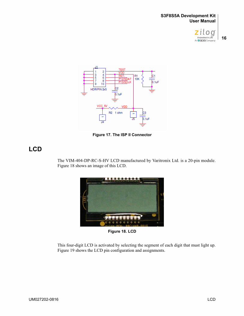
ISP II ConnectorThe ISP II connector (J1) provides an interface between the S3 Flash ISP II tool and the S3F8S5A device. See Figure 17 for an illustration of the ISP II connector.
Figure 15. Magnetic Buzzer
Figure 16. The Reset Circuit
UM027202-0816 Reset Circuit
S3F8S5A Development KitUser Manual
16
LCDThe VIM-404-DP-RC-S-HV LCD manufactured by Varitronix Ltd. is a 20-pin module. Figure 18 shows an image of this LCD.
This four-digit LCD is activated by selecting the segment of each digit that must light up. Figure 19 shows the LCD pin configuration and assignments.
Figure 17. The ISP II Connector
Figure 18. LCD
UM027202-0816 LCD

S3F8S5A Development KitUser Manual
17
Serial EEPROMThe 93C56B is enabled through the Chip Select pin (CS) and accessed via a 3-wire serial interface consisting of Data Input (DI), Data Output (DO), and Shift Clock (SK). Upon receiving a Read instruction at DI, the address is decoded, and the data is clocked out seri-ally on the DO pin. Figure 20 shows the Serial EEPROM schematics.
Figure 19. LCD Pin Configuration and Assignments
Figure 20. Serial EEPROM
UM027202-0816 Serial EEPROM

S3F8S5A Development KitUser Manual
18
ZDS Flash Loader UtilityA Flash Loader utility is included in Zilog Developer Studio II via the Tools menu. Figure 21 shows an image of the Flash Programming screen.
You can program the S3F8S5A MCU directly using the hex code generated from the ZDS IDE tools.
Figure 21. The Flash Programming Screen
UM027202-0816 ZDS Flash Loader Utility

S3F8S5A Development KitUser Manual
19
S3F8S5A Development Kit DocumentationThe documents associated with the S3F8S5A Development Kit are listed in Table 1. Each of these documents can be obtained from the Zilog website by clicking the link associated with its Document Number. Alternatively, navigate to the directory listed in the Location column in your installed application.
S3F8S5A Sample ProjectsTable 2 lists the sample projects developed for this application. Follow the filepath stated in the Location column to access the associated project.
Table 1. S3F8S5A Development Kit Documentation
Document Description LocationUM0272 S3F8S5A Development Kit User Manual Documentation\Tools_DocumentationPS0323 S3F8S5A Product Specification Documentation\Chip_DocumentationUM0266 S3 Flash In-System Programmer User Manual Documentation\Tools_DocumentationFL0170 S3F8S5A0100ZCOG Development Kit Insert Documentation\Tools_DocumentationFL0165 S3 Flash In-System Programmer Insert Documentation\Tools_DocumentationOnline Help ZDS II-S3 IDE, Assembler and C Compiler On-Line
HelpZDS II-S3 >Help >Help Topics
Table 2. S3F8S5A Sample Projects
Project LocationtimerD samples\S3F8S5A\ISP_BL_Demolcd samples\S3F8S5A\LCD_asmlcd samples\S3F8S5A\LCD_cledblink samples\S3F8S5A\ledblink_asmledblink samples\S3F8S5A\ledblink_ceeprom samples\S3F8S5A\EEPROM_c
UM027202-0816 S3F8S5A Development Kit Documentation

UM0272 20
S3F8S5A Development KitUser Manual
Appe
TEST
7 IN - DEFAULT0 IS USED
CKOI
P27/TXD0
P26/RXD0
P36/RXD1
P37/TXD1TXDRXD
P40/INT4/SEG12
VDD
VCC_5V
VDD
J8
1x6 RT-ANGL
123456
SW2B3U-1000P
12
D6LL4148
21
U2
93C56B
CS1
SK2
DI3
DO4
GND5ORG6NC7VCC8
R6 0 ohm
J3
HDR/PIN 1x11
1234567891011
R7 0 ohm
R13
100K
R8 0 ohm
C7
0.1uF
J7
12345678910
R9 0 ohm
02-0816
ndix A. Schematic DiagramsFigure 22 presents schematic diagrams of the S3F8S5A Development Board.
Figure 22. S3F8S5A Development Board Schematic Diagram
Current measurement
BENCH POWER
R6, RUART
VDD
TESTXIN
GNDXOUT
XTINXTOUT
RST-
XOUT
P13/SCLK
VDD
P12/SDATRST-
VCC_5V
XTin
XTout
XIN
RST-
P13/SCLKP12/SDAT
TEST
VDD
P37/TXD1P36/RXD1
P03/AD3
P26/RXD0P27/TXD0
P11/BUZP10/TAPWM
P00/COM0P01/COM1P02/COM2
P30/SEG4P31/SEG5P32/SEG6P33/SEG7P34/SEG8
P40/INT4/SEG12P41/SEG13P42/SEG14P43/SEG15P44/SEG16P45/SEG17P46/SEG18P47/SEG19
P03/AD3
P00/COM0
P01/COM1
P02/COM2
P30/SEG4P31/SEG5P32/SEG6P33/SEG7
P34/SEG8
P42/SEG14P41/SEG13
P43/SEG15P44/SEG16P45/SEG17P46/SEG18P47/SEG19
P25/SCKP24/SOP23/SIP15/EE_SEL
P25/SP24/SP23/S
P15/EE_SEL
P35/TCPWM
P20/TBPWMP21/PWMP22/TD0PWMP14
P10/TAPWM
P20/TBPWM
P35/TCPWM
VCC_5V
P11/BUZ
VDD
VDD
VCC_5V
VCC_5V
VCC_5V
VDD
J4
1
C11
0.01uF
C3
0.1uF
Y232.768KHZ
LED4
YELLOW
2 1
C1
0.1uF
Y1
12MHZ
SW1B3U-1000P
12
R45K
13
2
R2 1 ohm
1
2 3
4
U1
S3F8S5A
P1.0/INT0/TAOUT/TAPWM/SEG201
P1.1/INT1/TACLK/BUZ/SEG212
P1.2/INT2/TACAP/SDAT3
P1.3/INT3/TD1OUT/TD1PWM/SCLK4
VDD5
VSS6
Xout7
Xin8
TEST9
P1.6/XTIN10
P1.7/XTOUT11
/RESET12
P2.0/TBPWM/TD0CLK13
P2.1/PWM/TD0CAP14
P2.2/TD0OUT/TD0PWM/AD415
P1.4/TD1CLK/AD516
P1.5/TD1CAP/AD617
P2.3/AD7/SI18
P2.4/SO/SEG019
P2.5/SCK/SEG120
P2.6/RXD0/SEG221
P2.7/TXD0/SEG322
AVREF23AVSS24P0.0/COM0/AD025P0.1/COM1/AD226P0.2/COM2/AD227P0.3/COM3/AD328P3.0/PG0/SEG429P3.1/PG1/SEG530P3.2/PG2/SEG631P3.3/PG3/SEG732P3.4/PG4/SEG833
P3.5/TCOUT/TCPWM/PG5/SEG934P3.6/RXD1/PG6/SEG1035P3.7/TXD1/PG7/SEG1136P4.0/INT4/SEG1237P4.1/INT5/SEG1338P4.2/INT6/SEG1439P4.3/INT7/SEG1540P4.4/COM4/SEG1641P4.5/COM5/SEG1742P4.6/COM6/SEG1843P4.7/COM7/SEG1944
P1
USB, mini B
VBUS1
DM2
DP3
ID4
GND5
SH16
SH27
SH38
SH49
h110
h211
C418pF
J1
HDR/PIN 2x5
1 23 45 67 89 10
U5
CEM1206S
+1
-2
J9
123
D5
LL4148
21
LED2
GREEN
2 1
R4233.2
C6
18pF
C8
0.1uF
R10
470
J2
123456789
1011
LCD1
VIM-404
NC01
NC12
NC23
1B/1C/1P4
2B/2C/2P5
3B/3C/3P6
4B/4C7
COM38
NC39
NC410
COM1114D/4G/4A124E/4F133D/3G/3A143E/3F152D/2G/2A162E/2F171D/1G/1A181E/1F19COM220
J10
123
R3
100K
R5
470 C10
0.1uF
Q3MMSS8050
3
1
2
L1
FERRITE BEAD
R11
470
C5
0.1uF
R2433.2
LED3
RED
2 1
C9
4.7uF
R110K
J5
1
R12
470
J6
HDR/PIN 1x11
123456789
1011
LED1
GREEN
21
C2
0.1uF

S3F8S5A Development KitUser Manual
21
Customer SupportTo share comments, get your technical questions answered, or report issues you may be experiencing with our products, please visit Zilog’s Technical Support page at http:/support.zilog.com.
To learn more about this product, find additional documentation, or to discover other fac-ets about Zilog product offerings, please visit the Zilog Knowledge Base or consider par-ticipating in the Zilog Forum.
This publication is subject to replacement by a later edition. To determine whether a later edition exists, please visit the Zilog website at http://www.zilog.com/
UM027202-0816 Customer Support