SmartFusion2 Development Kit User Guide - Microsemi
98
SmartFusion2 SoC FPGA Development Kit User’s Guide
Transcript of SmartFusion2 Development Kit User Guide - Microsemi

SmartFusion2 SoC FPGA Development Kit
User’s Guide


SmartFusion2 SoC FPGA Development Kit User’s Guide
SmartFusion2 SoC FPGA Development Kit User’s Guide 3
Table of Contents
1 – Introduction .............................................................................................. 5 Kit Contents ................................................................................................................................ 5 SmartFusion2 SoC FPGA Development Kit Web Resources.................................................... 5 Board Description ....................................................................................................................... 5
2 – Installation and Settings ....................................................................... 11 Software Installation ................................................................................................................. 11 Hardware Installation ............................................................................................................... 11 Power Sources ......................................................................................................................... 22 Testing the Hardware ............................................................................................................... 23
3 – Key Components Description and Operation ..................................... 25 Powering Up the Board ............................................................................................................ 25 Current Measurement .............................................................................................................. 25 Memory Interface ..................................................................................................................... 27 SERDES0 Interface ................................................................................................................. 30 SERDES1 Interface ................................................................................................................. 31 MAX24288−10/100/1000 and Time Stamping ......................................................................... 33 PoE Interface ........................................................................................................................... 34 ADC Interface ........................................................................................................................... 35 RS232 Interface ....................................................................................................................... 35 RS485 Interface ....................................................................................................................... 36 CAN Interface ........................................................................................................................... 36 USB Interface ........................................................................................................................... 37 Marvell PHY (88E1340S) ......................................................................................................... 37 Programming ............................................................................................................................ 39 FTDI Interface .......................................................................................................................... 41 System Reset ........................................................................................................................... 42 Clock Oscillator ........................................................................................................................ 43 Debugging ................................................................................................................................ 43 FMC Connector Pin Out ........................................................................................................... 45
4 – Pin List .................................................................................................... 59
5 – Board Components Placement ............................................................. 85
6 – Demo Design .......................................................................................... 89 SF2-DEV-KIT-PP Board Demo Design.................................................................................... 89
7 – Manufacturing Test ................................................................................ 91 SF2-DEV-KIT-PP Board Testing Procedures .......................................................................... 91
List of Changes ............................................................................................ 93

Table of Contents
4 SmartFusion2 SoC FPGA Development Kit User’s Guide
Product Support .......................................................................................... 95 Customer Service ..................................................................................................................... 95 Customer Technical Support Center ........................................................................................ 95 Technical Support .................................................................................................................... 95 Website .................................................................................................................................... 95 Contacting the Customer Technical Support Center ............................................................... 95 ITAR Technical Support ........................................................................................................... 96

SmartFusion2 SoC FPGA Development Kit User’s Guide 5
1 – Introduction
The SmartFusion®2 SoC FPGA Development Kit (SF2-DEV-KIT-PP) is RoHS compliant and enables designers to develop applications that involve one or more of the following:
• Microprocessor applications • Embedded ARM® Cortex™-M3 processor based systems • Motor control • System management • Time stamping and SyncE applications • Power over Ethernet (PoE) • Industrial automation • High speed I/O applications • Universal serial bus (USB) applications (OTG support)
Kit Contents Table 1 lists the contents of the SmartFusion2 Development Kit.
Table 1. Kit Contents Quantity Description
1 SmartFusion2 Development Board with M2S050T-FGG896
1 FlashPro4 programmer
1 USB A to micro B cable
1 USB Micro A to A cable
1 USB A to mini B cable
1 PCIe edge card ribbon cable
1 12 V power adapter
SmartFusion2 SoC FPGA Development Kit Web Resources SmartFusion2 Development Kit web resources are available: www.microsemi.com/soc/products/hardware/devkits_boards/smartfusion2_dev.aspx#rsc.
Board Description The SmartFusion2 SoC FPGA Development Kit offers a full-featured development board for SmartFusion2 system-on-chip (SoC) FPGAs. This kit inherently integrates reliable flash-based FPGA fabric, a 166 MHz Cortex-M3 processor, advanced security processing accelerators, digital signal processing (DSP) blocks, static random-access memory (SRAM), embedded nonvolatile memory (eNVM), and industry-required high-performance communication interfaces—all on a single chip. The board has numerous standard peripherals such as USB, Philips inter-integrated circuit (I2C), serial peripheral interface (SPI), RS232, controller area network (CAN), Ethernet, and RS485. The board has the option to be powered through PoE, includes a 16-bit analog-to-digital converter (ADC) and has IEEE 1588 packet time-stamping capabilities.
1 – Introduction
6 SmartFusion2 SoC FPGA Development Kit User’s Guide
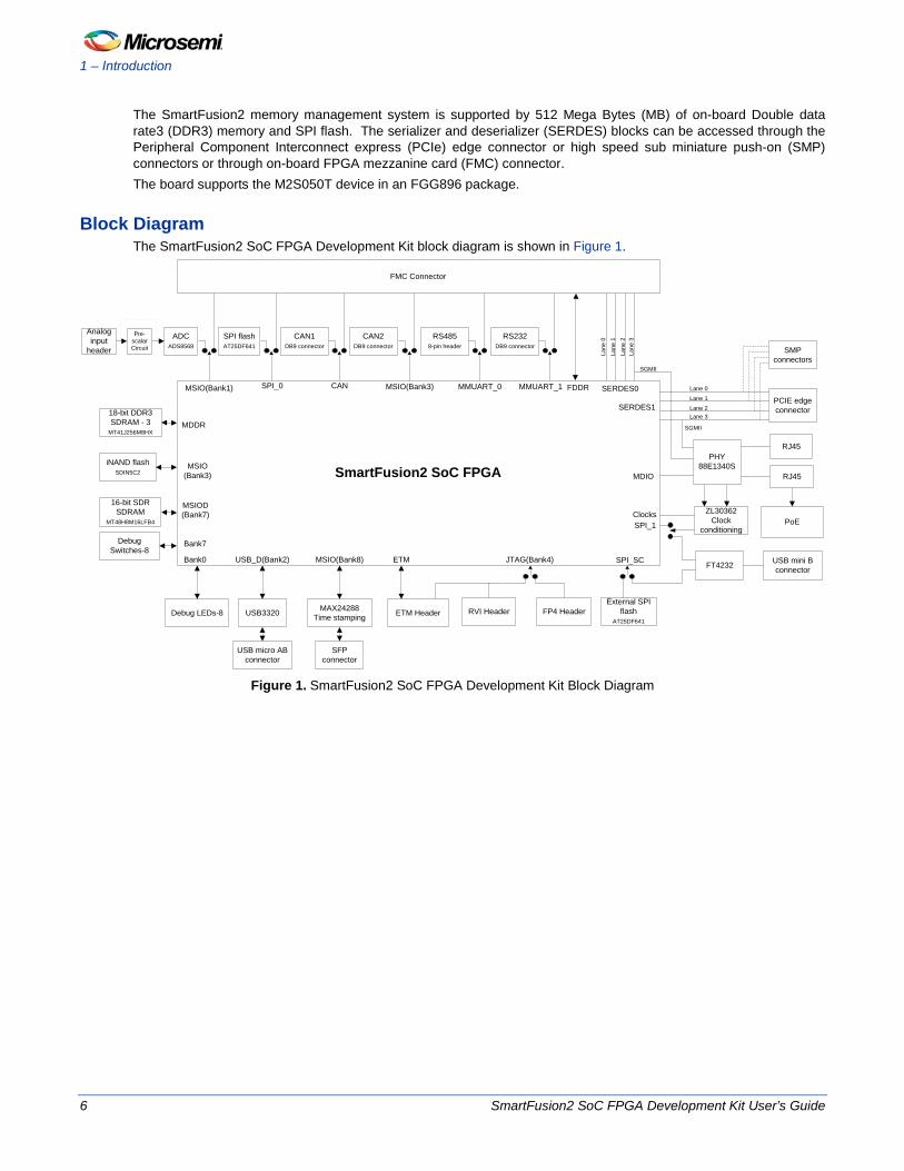
The SmartFusion2 memory management system is supported by 512 Mega Bytes (MB) of on-board Double data rate3 (DDR3) memory and SPI flash. The serializer and deserializer (SERDES) blocks can be accessed through the Peripheral Component Interconnect express (PCIe) edge connector or high speed sub miniature push-on (SMP) connectors or through on-board FPGA mezzanine card (FMC) connector. The board supports the M2S050T device in an FGG896 package.
Block Diagram The SmartFusion2 SoC FPGA Development Kit block diagram is shown in Figure 1.
SmartFusion2 SoC FPGA
FMC Connector
ADCADS8568
PHY88E1340S
RJ45
RJ45
PCIE edge connector
SMP connectors
PoE
FP4 HeaderRVI HeaderETM Header
SFP connector
USB3320
16-bit SDR SDRAM
MT48H8M16LFB4
MAX24288Time stamping
ZL30362Clock
conditioning
FT4232
External SPI flash
AT25DF641
Lane 3Lane 2Lane 1Lane 0
Lane
0La
ne 1
Lane
2La
ne 3
Analog input
header
SPI_0MSIO(Bank1)
MSIO (Bank3)
MSIOD (Bank7)
CAN MSIO(Bank3)
USB_D(Bank2)
MMUART_1MMUART_0
USB micro AB connector
MSIO(Bank8) USB mini B connector
SPI_1
SGMII
SGMII
FDDR SERDES0
SERDES1
CAN1DB9 connector
SPI flashAT25DF641
CAN2DB9 connector
18-bit DDR3 SDRAM - 3
MT41J256M8HXMDDR
RS4858-pin header
RS232DB9 connector
JTAG(Bank4) SPI_SC
Debug LEDs-8
Bank0 ETM
MDIO
Debug Switches-8
Bank7
iNAND flashSDIN5C2
Pre-scalar Circuit
Clocks
Figure 1. SmartFusion2 SoC FPGA Development Kit Block Diagram

1 – Introduction
SmartFusion2 SoC FPGA Development Kit User’s Guide 7
Board Overview Figure 2 shows an overview of the board features.
Figure 2. SmartFusion2 SoC FPGA Development Kit Board Overview
I/O Voltage Rails Table 2. I/O Voltage Rails
SmartFusion2 Bank I/O Rail Voltage
Bank0 VDDIO0_1P5V 1.5 V
Bank1 VDDIO1_3P3V 3.3 V
Bank2 VDDIO2_3P3V 3.3 V
Bank3 VDDIO3_3P3V 3.3 V
Bank4 VDDIO4_3P3V 3.3 V
Bank5 VDDIO5_2P5V 2.5 V
Bank6 VDDIO6_2P5V 2.5 V
Bank7 VDDIO7_1P8V 1.8 V

1 – Introduction
8 SmartFusion2 SoC FPGA Development Kit User’s Guide
SmartFusion2 Bank I/O Rail Voltage
Bank8 VDDIO8_3P3V 3.3 V
Bank9 VDDIO9_2P5V 2.5 V
Table 3 describes SmartFusion2 SoC FPGA Development Kit board components.
Table 3. SmartFusion2 SoC FPGA Development Kit Board Components Name Description
M2S050T-FGG896 Microsemi SmartFusion2 SoC FPGA with hard Cortex-M3 processor.
DDR3 synchronous dynamic random access memory (SDRAM)
• 512 MB (2x256 MB Micron DDR3 memory MT41J256M8HX-15E) for storing the data bits • 256 MB (1x256 MB Micron DDR3 memory MT41J256M8HX-15E) for storing the ECC bits
Single data rate (SDR) SDRAM
16 MB low power mobile SDRAM Micron MT48H8M16LFB4 connected to the SmartFusion2 bank7 I/Os.
iNAND flash 4 GB iNAND flash SanDisk SDIN5C2-4G connected to the SmartFusion2 bank3 I/Os.
SPI flash 8 MB SPI flash Atmel AT25DF641-MWH-T connected to SPI port 0 of the SmartFusion2 SoC FPGA MSS.
ADC 16-bit, 8-channel ADC ADS8568
Ethernet RJ45 connector (Ethernet jack with magnetics) interfacing with Marvell 10/100/1000 BASE-T PHY chip 88E1340S in SGMII mode, interfacing with the Ethernet port of the SmartFusion2 MSS (on-chip MAC and external PHY).
10/100/1000 and Time stamping
MAX24288, the IEEE 1588 clock and time stamper with a serial gigabit media independent interface (SGMII) or 1000BASE-X serial interface and a parallel media independent interface (MII) that can be configured for gigabit media independent interface (GMII), reduced gigabit media independent interface (RGMII), or 10/100 MII.
PoE RJ45 connector (J4) interfacing with IEEE 802.3at compliant Microsemi device PD70201 and step-down transformer to generate the 12 V power supply.
RS485 RS485 with 8-pin connector (J221) interfacing with SN65HVD12D, connected to UART port 0 of the SmartFusion2 MSS.
RS232 RS232 with DB9 female connector interfacing with SN65C3221EPWR, connected to UART port 1 of the SmartFusion2 MSS.
CAN interface1 CAN interface with DB9 male connector (J42) interfacing with MAX3051 CAN transceiver connected to CAN controller of the SmartFusion2 MSS.
CAN interface2 CAN interface with DB9 male connector (J113) interfacing with MAX3051 CAN transceiver connected to four general purpose I/Os (GPIOs) of the SmartFusion2 MSS.
RVI header RVI header for application programming and debug from Keil ULINK or IAR J-Link.
FP4 header Flashpro4 programming header for SmartFusion2 programming and debugging with Microsemi tools.
Future Technology Devices International (FTDI) programmer
FTDI programmer interface (J24) to program the external SPI flash and ZL30362 clock conditioning chip. An FTDI chip is also used to change the JTAG_SEL signal (High or Low) remotely for switching between RVI header and JTAG mode.
Embedded trace macro (ETM) cell header
ETM header for debug.
Small form-factor pluggable (SFP) connector
SFP connector for high speed communication interfaces such as gigabit Ethernet and fibre channel.

1 – Introduction
SmartFusion2 SoC FPGA Development Kit User’s Guide 9
Name Description
PCIe edge connector PCI Express edge connector with 4 lanes
Dual in-line package (DIP) switches
Debug switches for user application.
Light-emitting diodes (LEDs)
8 active High LEDs that are connected to some of the user I/Os for debug.
Push–button reset Push-button system reset for SmartFusion2 system.
Push–button switches 6 push-button switches for test and navigation.
FMC connector FMC header to connect the external daughter boards.
USB interface USB micro AB connector, interfacing with the high speed USB2.0 ULPI transceiver chip USB3320, interfacing with USB-D port of the SmartFusion2 MSS.
Clock conditioning ZL30362 clock conditioning for providing synchronous clocks to Ethernet PHY and time-stamping circuits.
OSC-100 100 MHz clock oscillator (differential output)
OSC-50 50 MHz clock oscillator
OSC-32 32.768 KHz low power oscillator


SmartFusion2 SoC FPGA Development Kit User’s Guide 11
2 – Installation and Settings
Software Installation Download and install the latest release of Microsemi Libero® System-on-Chip (SoC) software v11.0 or later, from the Microsemi website and register for a free Gold license. For instructions on how to install Libero SoC and SoftConsole, refer to the Libero Installation and Licensing Guide, available on the Microsemi website. Refer to the Installing IP Cores and Drivers User’s Guide to download and install Microsemi DirectCores, SGCores, and driver firmware cores. These must be localized on the PC where Microsemi Libero SoC is installed while designing with Microsemi FPGAs and SoCs. Microsemi has partnered with key industry leaders in the microcontroller space to provide a robust SmartFusion2 ecosystem. SmartFusion2 is supported by the latest release of the IAR® Embedded Workbench™ from IAR Systems for ARM. The Microsemi SmartFusion2 SoC FPGA is also supported by the latest release of Keil, the MDK-ARM Microcontroller Development Kit.
Hardware Installation The FlashPro3/FlashPro4 programmer can be used to program the SF2-DEV-KIT-PP board.
Jumpers, Switches, LEDs, and DIP Switch Settings The recommended default jumpers, switches, LEDs, and DIP switch settings are defined in Table 4 through Table 6.
• Table 4. Jumper Settings • Table 5. LEDs • Table 6. Test Points
Connect the jumpers with the default settings to enable the pre-programmed demonstration design to function correctly. Note: Location of all the jumpers and test points are searchable in Figure 27 (page 86) of 5 – Board Components
Placement section. Table 4. Jumper Settings
Jumper Function Default Settings Notes
Power Supply
J2
Jumper to select the power supply option
Pin 1–2 PoE Open
Pin 1–3 External DC Jack Closed
Pin 1–4 PCIe Open
J23
Jumper to select the core voltage (VDD_REG) to either 1.0 V or 1.2 V
Pin 1–2 for 1.0 V core voltage Open
Pin 2–3 for 1.2 V core voltage Closed
J117 Jumper to connect 3P3V_LDO to PLLFDDRVDDA 1–2 Closed
J123 Jumper to connect VDD_REG to PCIExVDD 1–2 Closed
J142 Jumper to connect 3P3V_LDO to PLLPCIExVDDA 1–2 Closed

2 – Installation and Settings
12 SmartFusion2 SoC FPGA Development Kit User’s Guide
Jumper Function Default Settings Notes
J157 Jumper to connect 3P3V_LDO to VPPNVMSA0 1–2 Closed
J160 Jumper to connect VDD_REG to PCIExVDDIOx 1–2 Closed
J167 Jumper to connect 2P5V_LDO to PCIExVDDPLL 1–2 Closed
J225 Jumper to connect 3P3V_LDO to PLLMDDRVDDA 1–2 Closed
J226 Jumper to connect 3P3V_LDO to PLLXVDDA 1–2 Closed
J227 Jumper to connect 3P3V_LDO to VPP 1–2 Closed Programming and Debugging
J38
Jumper to select either Low or High to On_Board_REFLASH
Pin 1-2 High − FLASH_GOLDEN_N for not IAP mode. Open
Pin 2-3 Low − FLASH_GOLDEN_N for IAP mode. Close
J43
Jumper to select On_Board_REFLASH signal or n_FTDI_TRST to SPI_REFLASH (FLASH_GOLDEN_N).
Pin 1-2 n_FTDI_TRST to SPI_REFLASH Open
Pin 2-3 On_Board_REFLASH to SPI_REFLASH Open
J55 Jumper to enable the MUX to pass the SPI flash programming mode signal (to enable the Quad 1-of-2 multiplexer/demultiplexer) Open
J70
Device reset generation selection
Pin 1-2 Reset depends on 3.3 V rail Closed
Pin 2-3 Reset depends on FLASH_GOLDEN pin Open
J71
Jumper to enable or disable the SPI programming mode
Pin 1-2 3.3 V disable Open
Pin 2-3 GND enable Open
J93
JTAG selection jumper to select between RVI header or FP4 header for application debug
Pin 1-2 FP4 for SoftConsole/FlashPro Closed
Pin 2-3 RVI for Keil ULINK™/IAR J-Link® Open
J94
Jumper to select the JTAG reset
Pin 1-2 selects reset from FP4 header/RVI header depending on JTAG selection Closed
Pin 2-3 for SPI flash programming mode Open SFP Connector
J8 Jumper to connect the SFP connector’s clock for serial ID interface to SmartFusion2 I/O (U6). Open
J9 Jumper to connect the SFP connector’s DATA for serial ID interface to SmartFusion2 I/O (T9). Open
J10 Jumper to select the SFP connector optical output (Short 1-2). Open
J11 Jumper to select the bandwidth option for SFP transceiver

2 – Installation and Settings
SmartFusion2 SoC FPGA Development Kit User’s Guide 13
Jumper Function Default Settings Notes
Pin 1-2 3.3 V (High bandwidth) Open
Pin 2-3 GND (reduced bandwidth) Open CAN1
J36 Parallel termination 120Ω for CAN1 signals. Open
J52 CAN1 (DB9 connector) shield to ground connection. Open
J111
Jumper to select between CAN1 bus Rx and FMC_V24
Pin 1-2 CAN1 Open
Pin 2-3 FMC Open
J114
Jumper to select between CAN1 bus Tx and FMC_AA28.
Pin 1-2 CAN1 Open
Pin 2-3 FMC Open
J115
Jumper to select between CAN1 TXEBL and FMC_AA29.
Pin 1-2 CAN1 Open
Pin 2-3 FMC Open CAN2
J109 Parallel termination 120Ω for CAN2 signals. Open
J120 CAN2 (DB9 connector) shield to ground connection. Open
J131
Jumper to select between CAN2 TXEBL and FMC_T27.
Pin 1-2 CAN2 Open
Pin 2-3 FMC Open
J134
Jumper to select between CAN2 bus Rx and FMC_T26.
Pin 1-2 CAN2 Open
Pin 2-3 FMC Open
J232
Jumper to select between CAN2 bus Tx and FMC_U24.
Pin 1-2 CAN2 Open
Pin 2-3 FMC Open SPI_0
J110
Jumper to select between SPI flash SCK and FMC_V22.
Pin 1-2 SPI flash Open
Pin 2-3 FMC Open
J118
Jumper to select between SPI flash SDO and FMC_W27.
Pin 1-2 SPI flash Open
Pin 2-3 FMC Open
J119 Jumper to select between SPI flash SDI and FMC_Y30.
Pin 1-2 SPI flash Open

2 – Installation and Settings
14 SmartFusion2 SoC FPGA Development Kit User’s Guide
Jumper Function Default Settings Notes
Pin 2-3 FMC Open
J121 Jumper to select between SPI flash SS and FMC_W28.
Pin 1-2 SPI flash Open
Pin 2-3 FMC Open SPI_1
J20 Jumper to select between ZL30362 SPI_CS and FT4232 SPI_CS.
Pin 1-2 ZL30362 Open
Pin 2-3 FT4232 Open
J21 Jumper to select between ZL30362 SPI_SCL and FT4232 SPI_SCL.
Pin 1-2 ZL30362 Open
Pin 2-3 FT4232 Open
J22 Jumper to select between ZL30362 SPI_SO and FT4232 SPI_SI.
Pin 1-2 ZL30362 Open
Pin 2-3 FT4232 Open
J25 Jumper to select between ZL30362 SPI_SI and FT4232 SPI_SO.
Pin 1-2 ZL30362 Open
Pin 2-3 FT4232 Open
J54 Jumper to select between ZL30362 reset and FT4232 reset from VSS of SmartFusion2 device.
Pin 1-2 ZL30362 Open
Pin 2-3 FT4232 Open
J129 Jumper to select between FT4232 DD0 and FMC_R29 to SPI_1_SS1.
Pin 1-2 FMC Open
Pin 2-3 FT4232 Open
J133 Jumper to select between FT4232 DD1 and FMC_R24 to SPI_1_SS2.
Pin 1-2 FMC Open
Pin 2-3 FT4232 Open USB
J139 Jumper to select between USB reset and FMC_P24.
Pin 1-2 USB Open
Pin 2-3 FMC Open
J163 Jumper to select the USB mode of operation.
Pin 1-2 On-The-Go (OTG) mode Open
Pin 2-3 Either host or device mode Open
J164 Jumper to provide the VBUS supply to USB when using in Host mode. 1–2 Open

2 – Installation and Settings
SmartFusion2 SoC FPGA Development Kit User’s Guide 15
Jumper Function Default Settings Notes
ADC
J122 Jumper to select between ADS8568_REFEN and FMC_M23.
Pin 1-2 ADS8568_REFEN Open
Pin 2-3 FMC Open
J137 Jumper to enable or disable the generation of HVDD and HVSS.
Pin 1-2 Enable Open
Pin 2-3 Disable Open
J138 Jumper to select between ADC CONVST_D and FMC_P23 from SmartFusion2 I/O P23 pin.
Pin 1-2 ADC CONVST_D Open
Pin 2-3 FMC_P23 Open
J140 Jumper to select between ADC CONVST_C and FMC_N25 from SmartFusion2 I/O N25 pin.
Pin 1-2 ADC CONVST_C Open
Pin 2-3 FMC_N25 Open
J141 Jumper to select between ADC CONVST_B and FMC_N26 from SmartFusion2 I/O N26 pin.
Pin 1-2 ADC CONVST_B Open
Pin 2-3 FMC_N26 Open
J144 Jumper to select between ADC BUSY and FMC_M27 from SmartFusion2 I/O M27 pin.
Pin 1-2 ADC BUSY Open
Pin 2-3 FMC_M27 Open
J146 Jumper to select between ADC DB7 and FMC_L29 from SmartFusion2 I/O L29 pin.
Pin 1-2 ADC DB7 Open
Pin 2-3 FMC_L29 Open
J154 Jumper to select between ADC DB1 and FMC_L30 from SmartFusion2 I/O L30 pin.
Pin 1-2 ADC DB1 Open
Pin 2-3 FMC_L30 Open
J155 Jumper to select between ADC DB2 and FMC_L28 from SmartFusion2 I/O L28 pin.
Pin 1-2 ADC DB2 Open
Pin 2-3 FMC_L28 Open
J158 Jumper to select between ADC DB3 and FMC_K29 from SmartFusion2 I/O K29 pin.
Pin 1-2 ADC DB3 Open

2 – Installation and Settings
16 SmartFusion2 SoC FPGA Development Kit User’s Guide
Jumper Function Default Settings Notes
Pin 2-3 FMC_K29 Open
J159 Jumper to select between ADC DB4 and FMC_K30 from SmartFusion2 I/O K30 pin.
Pin 1-2 ADC DB4 Open
Pin 2-3 FMC_K30 Open
J161 Jumper to select between ADC SEL_CD and FMC_K28 from SmartFusion2 I/O K28 pin.
Pin 1-2 ADC SEL_CD Open
Pin 2-3 FMC_K28 Open
J175 Jumper to select between ADC DB8 and FMC_L26 from SmartFusion2 I/O L26 pin.
Pin 1-2 ADC DB8 Open
Pin 2-3 FMC_L26 Open
J176 Jumper to select the analog input (6th pin of J216 header) to channel B0 of 16-bit ADC with filtering or without filtering.
Pin 1-2 direct analog input Open
Pin 2-3 with pre-scalar circuit Open
J179 Jumper to select between ADC SDI and FMC_H26 from SmartFusion2 I/O H26 pin.
Pin 1-2 ADC SDI Open
Pin 2-3 FMC_H26 Open
J180 Jumper to select the analog input (2nd pin of J216 header) to channel A0 of 16-bit ADC with filtering or without filtering.
Pin 1-2 direct analog input Open
Pin 2-3 with pre-scalar circuit Open
J181 Jumper to select the analog input (4th pin of J216 header) to channel A1 of 16-bit ADC with filtering or without filtering.
Pin 1-2 direct analog input Open
Pin 2-3 with pre-scalar circuit Open
J183 Jumper to select between ADC DB11 and FMC_J30 from SmartFusion2 I/O J30 pin.
Pin 1-2 ADC DB11 Open
Pin 2-3 FMC_J30 Open
J184 Jumper to select between ADC DB0 and FMC_J29 from SmartFusion2 I/O J29 pin.
Pin 1-2 ADC DB0 Open
Pin 2-3 FMC_J29 Open
J187 Jumper to select between ADC serial output pin SDO_A and FMC_J28 from SmartFusion2 I/O J28 pin.

2 – Installation and Settings
SmartFusion2 SoC FPGA Development Kit User’s Guide 17
Jumper Function Default Settings Notes
Pin 1-2 ADC SDO_A Open
Pin 2-3 FMC_J28 Open
J193 Jumper to select the HW/SW pin of 16-bit ADC to High or low.
Pin 1-2 High Open
Pin 2-3 Low Open
J196 Jumper to select between ADC serial output pin SDO_C and FMC_G30 from SmartFusion2 I/O G30 pin.
Pin 1-2 ADC SDO_C Open
Pin 2-3 FMC_G30 Open
J200 Jumper to select between ADC serial output pin SDO_D and FMC_F30 from SmartFusion2 I/O F30 pin.
Pin 1-2 ADC SDO_D Open
Pin 2-3 FMC_F30 Open
J201 Jumper to select between ADC CSN and FMC_M25 from SmartFusion2 I/O M25 pin.
Pin 1-2 ADC CSN Open
Pin 2-3 FMC_M25 Open
J202 Jumper to select between ADC RDN and FMC_K25 from SmartFusion2 I/O K25 pin.
Pin 1-2 ADC RDN Open
Pin 2-3 FMC_K25 Open
J203 Jumper to select the RANGE/XCLK pin of 16-bit ADC to High or Low.
Pin 1-2 High Open
Pin 2-3 Low Open
J204 Jumper to select the analog input (8th pin of J216 header) to channel B1 of 16-bit ADC with filtering or without filtering.
Pin 1-2 direct analog input Open
Pin 2-3 with pre-scalar circuit Open
J212 Jumper to select the analog input (12th pin of J216 header) to channel C1 of 16-bit ADC with filtering or without filtering.
Pin 1-2 direct analog input Open
Pin 2-3 with pre-scalar circuit Open
J214 Jumper to select between ADC RESET and FMC_N23 from SmartFusion2 I/O N23 pin.
Pin 1-2 ADC RESET Open
Pin 2-3 FMC_N23 Open
J215 Jumper to select the parallel or serial interface mode of 16-bit ADC.
Pin 1-2 serial interface Open

2 – Installation and Settings
18 SmartFusion2 SoC FPGA Development Kit User’s Guide
Jumper Function Default Settings Notes
Pin 2-3 parallel interface Open
J217 Jumper to select the analog input (14th pin of J216 header) to channel D0 of 16-bit ADC with filtering or without filtering.
Pin 1-2 direct analog input Open
Pin 2-3 with pre-scalar circuit Open
J218 Jumper to select the analog input (16th pin of J216 header) to channel D1 of 16-bit ADC with filtering or without filtering.
Pin 1-2 direct analog input Open
Pin 2-3 with pre-scalar circuit Open
J222 Jumper to select the analog input (10th pin of J216 header) to channel C0 of 16-bit ADC with filtering or without filtering.
Pin 1-2 direct analog input Open
Pin 2-3 with pre-scalar circuit Open MAX24288 Mode Selection
J103 Jumper to drive the GPO1 of MAX24288 to High or Low.
Pin 1-2 3.3 V Open
Pin 2-3 GND Open
J112 Test purpose of MAX24288
Pin 1-2 3.3 V Open
Pin 2-3 GND Open
J116 Jumper to drive the GPO2 of MAX24288 to High or Low.
Pin 1-2 3.3 V Open
Pin 2-3 GND Open
J132 Test purpose of MAX24288
Pin 1-2 3.3 V Open
Pin 2-3 GND Open
J156 Jumper to drive the GPIO1 of MAX24288 to High or Low.
Pin 1-2 3.3 V Open
Pin 2-3 GND Open
J166 Jumper to drive the GPIO2 of MAX24288 to High or Low.
Pin 1-2 3.3 V Open
Pin 2-3 GND Open
J177 Jumper to drive the GPIO3 of MAX24288 to High or Low.
Pin 1-2 3.3 V Open
Pin 2-3 GND Open

2 – Installation and Settings
SmartFusion2 SoC FPGA Development Kit User’s Guide 19
Jumper Function Default Settings Notes
MMUART_0
J178 Jumper to select between RS485_RE and FMC_J26.
Pin 1-2 RS485 Open
Pin 2-3 FMC Open
J199 Jumper to select between RS485_TX and FMC_H27.
Pin 1-2 RS485 Open
Pin 2-3 FMC Open
J209 Jumper to select between RS485_TE and FMC_M29.
Pin 1-2 RS485 Open
Pin 2-3 FMC Open
J210 Jumper to select between RS485_RX and FMC_L23.
Pin 1-2 RS485 Open
Pin 2-3 FMC Open MMUART_1
J188 Jumper to select between RS232_DIN and FMC_H30.
Pin 1-2 RS232 Open
Pin 2-3 FMC Open
J195 Jumper to select between RS232_INVALIDn and FMC_H28.
Pin 1-2 RS232 Open
Pin 2-3 FMC Open
J197 Jumper to select between RS232_ROUT and FMC_G29.
Pin 1-2 RS232 Open
Pin 2-3 FMC Open I2C_0
J172 Jumper to connect the I2C_0 SDA to pull-Up or FMC_K23.
Pin 1-2 Pull-Up Open
Pin 2-3 FMC Open
J173 Jumper to connect the I2C_0 SCL to pull-Up or FMC_K24.
Pin 1-2 Pull-Up Open
Pin 2-3 FMC Open
I2C_1
J135 Jumper to connect the I2C_1 SDA to pull-Up or FMC_V23.
Pin 1-2 Pull-Up Open
Pin 2-3 FMC Open

2 – Installation and Settings
20 SmartFusion2 SoC FPGA Development Kit User’s Guide
Jumper Function Default Settings Notes
MAX24288 SPI Interface
J151 Jumper to connect MAX24288’s SCLK pin to SmartFusion2 R5 pin Open
J152 Jumper to connect MAX24288’s SDI pin to SmartFusion2 R6 pin. Open
J153 Jumper to connect MAX24288’s SDO pin to SmartFusion2 R8 pin. Open
J182 Jumper to connect MAX24288’s CS_N pin to SmartFusion2 J3 pin. Open Marvell PHY
J33 Jumper to select either PHY_CONFIG1 or SF2_PHY_CONFIG1 for Global hardware configuration CONFIG[1]
Pin 1-2 CONFIG [1] will connect to clock conditioning circuit, HPOUTCLK4.
Open
Pin 2-3 CONFIG [1] will connect to SmartFusion2 MSIO112NB8. Open
J67 Jumper to short AC test points for debugging (datasheet recommends leaving it unconnected)
Open
ZL30362
J29 Jumper to isolate the ground connection to internal connection pin (datasheet recommends leaving it unconnected)
Open
J30 Jumper to select either High or Low to internal connection pin (datasheet recommends leaving it unconnected)
Pin 1-2 Connection to +3.3 V Open
Pin 2-3 Connection to ground Open
J228 DDRIO92NB0/CCC_NW0_I2 connects to ground through this jumper. Open
J229 DDRIO91PB0/GB0/CCC_NW0_I3 connects to ground through this jumper.
Open
Table 5. LEDs LED Comment
DS1 Indicates the 1.8 V rail.
DS2 Indicates the 1.5 V rail.
DS3 Indicates the 3.3_LDO V rail.
DS4 Indicates the 2.5_LDO V rail.
DS5 Indicates the 2.5 V rail.
DS6 Indicates the VDD_REG V rail.
DS7 Indicates the 12 V power supply.
DS8 Indicates the 5.0 V rail.
DS9 Indicates the 3.3 V rail.
DS10 Indicates detection of an IEEE 802.3at compliant (power sourcing equipment) (PSE).
DS11 Indicates that the power rails from PoE are ready.
DS12 Connected to parallel LED output port 0 (P0_LED[0]) of Marvell PHY.

2 – Installation and Settings
SmartFusion2 SoC FPGA Development Kit User’s Guide 21
LED Comment
DS13 Connected to parallel LED output port 0 (P0_LED[1]) of Marvell PHY.
DS14 Connected to parallel LED output port 0 (P0_LED[2]) of Marvell PHY.
DS15 Connected to parallel LED output port 0 (P0_LED[3]) of Marvell PHY.
DS16 Connected to parallel LED output port 1 (P0_LED[0]) of Marvell PHY.
DS17 Connected to parallel LED output port 1 (P0_LED[1]) of Marvell PHY.
DS18 Connected to parallel LED output port 1 (P0_LED[2]) of Marvell PHY.
DS19 Connected to parallel LED output port 1 (P0_LED[3]) of Marvell PHY.
DS20 Indicates receiving on CAN1.
DS21 Indicates transmitting on CAN1.
DS22 Connected to MAX24288. Indicates link status: 0=link down, 1=link up.
DS23 Indicates receiving on CAN2.
DS24 Indicates transmitting on CAN2.
DS25 Indicates the CRS (carrier sense) signal from MAX24288.
Table 6. Test Points Test Point Description
TP1 MODE_0 pin of SFP Connector.
TP2 TX_FAULT pin of SFP Connector.
TP3 VREF5
TP4 USB switch in/out for DP signal.
TP5 USB switch in/out for DM signal.
TP7 to TP14 GND
TP15 VDD_REG
TP16 5 V power supply
TP17 3.3 V
TP18 2.5 V
TP19 3.3 V_LDO
TP20 2.5 V_LDO
TP21 1.5 V
TP22 DDR3_VTT
TP23 1.8 V
TP24 VDD 1.2 V
TP25 PHY 1.0 V
TP26 VDDIO
TP27 HVDD
TP28 HVSS
TP29, TP30 GND

2 – Installation and Settings
22 SmartFusion2 SoC FPGA Development Kit User’s Guide
Power Sources The SmartFusion2 SoC FPGA Development board can be powered from three different sources:
• External DC jack (default) • PoE (will be available in the later version) • PCIe edge connector (will be available in the later version)
SmartFusion2 Power Sources Voltage rails (12 V, 5 V, 3.3 V, 2.5 V, 1.8 V, 1.5 V, 1.2 V, and 1.0 V) provided on the board are shown in Figure 3:
PTH08T230WAZ
NX7102
NX9415CMTR
VDD_REG/6A
5 V / 3 A
3.3 V / 5 A
MIC37102YM
3.3_LDO/ 1 A
MIC37102YM
2.5_LDO/ 1 A
MIC69502WR2.5 V / 5 A
MIC69502WR
DDR3_1P5 / 5 A
TPS51200 DDR3_VTT / 5 A
12 V
MIC69153YME
DVDD12 / 1.5 A
MIC69153YME
1P0_PHY V / 1.5 A
MIC69502WR
1.8 V / 5 A
PLLPCIEXVDDAVPPNVMSAOPLLXVDDA
PLLFDDRVDDAPLLMDDRVDDA
VPP
VDDIO6_2P5VDDIO9_2P5
PCIEXVDDPLL
PCIEXVDDVDD
PCIXVDDIO
VDDIO5_2P5
VDDIO7_1P8
VDDIO0_1P5VDDIO1_3P3VDDIO2_3P3VDDIO3_3P3VDDIO4_3P3VDDIO8_3P3
Figure 3. Voltage Rails in the SmartFusion2 SoC FPGA Development Kit
• PTH08T230WAZ, supplies VDD_REG rails. • NX7102 (5.0 V, 3 A), supplies 5.0 V rails. • NX9415CMTR (3.3 V, 5 A), supplies 3.3 V rails. • MIC37102YM (3.3 V, 1 A), supplies 3.3_LDO V rails. • MIC69502WR (2.5 V, 5 A), supplies 2.5 V rails. • MIC37102YM (2.5 V, 1 A), supplies 2.5_LDO V rails. • MIC69502WR (1.8 V, 5 A), supplies 1.8 V rails. • MIC69502WR (1.5 V, 5 A), supplies 1.5 V rails. • TPS51200 supplies DDR3_VTT rails. • MIC69153YME (1.2 V, 1.5 A), supplies 1.2 V rails.

2 – Installation and Settings
SmartFusion2 SoC FPGA Development Kit User’s Guide 23
• MIC69153YME (1.0 V, 1.5 A), supplies 1.0 V rails.
Testing the Hardware If the board is shipped directly from Microsemi, it contains a test program that determines whether or not the board works properly. If you suspect that the board is damaged, you can rerun the Manufacturing Test to verify the key interfaces of the board functionality. Refer to http://www.microsemi.com/soc/download/rsc/?f=%20SF2-DEV-KIT-PP_Mfg_PF (to be released) for manufacturing test procedures.


SmartFusion2 SoC FPGA Development Kit User’s Guide 25
3 – Key Components Description and Operation
This chapter describes the key component interfaces. For device datasheets, refer to: http://www.microsemi.com/soc/products/hardware/devkits_boards/smartfusion2_dev.aspx
Powering Up the Board The board can be powered by either one of the three 12 V sources, as shown in Figure 4. Currently, External DC Jack (12P0V_Ext) is only supported. To power up using External DC Jack (12P0V_Ext), do the following: External DC Jack (12P0V_Ext):
1. Make sure J2 connector 1 − 3 pads shorted (by default), as shown in Figure 4. 2. Check for Jumper − J23 short pins 2-3 3. Connect 12 V power supply brick to J18 to power the board. 4. Slide the main power switch SW7 to ON position.
1
23
4
12P0V_PoE12P0V_Ext12P0V_PCIe12P0V_IN
J2
2
5
1
3
46
12P0V
ENABLE_FT4232NL
SW7
Figure 4. Powering Up the Board
Current Measurement For applications which require current measurement, current sensing resistors/jumpers are provided on the SmartFusion2 Development Kit. For example, for VDD (1.2V) Voltage rail, the current measurement is performed across the headers J27 and J28 pins, as shown in the Figure 5. Since current measurement requires a high precision equipment, it is recommended to remove the current sense resistor RS1 (0.001 ohms) and measure current with a Fluke multi-meter (for example, 289) in series. Other available multi-meters can also be used. The current sensing circuit for the VDD (1.2 V) voltage rail is shown in Figure 5:
VDD VDD_REG
RS1
0.001
J28 J27
Figure 5. VDD Voltage Rail Current Measurement

3 – Key Components Description and Operation
26 SmartFusion2 SoC FPGA Development Kit User’s Guide
Table 7 lists the jumpers (2 pins) for all available on board power supplies: Table 7. Jumpers for Current Measurement
Power Supply Jumpers for Current Measurement
PLLPCIExVDDA J142
PLLXVDDA J226
PLLFDDRVDDA J117
PLLMDDRVDDA J225
VPP J227
VPPNVMSA0 J157
PCIExVDD J123
PCIExVDDIOx J160
PCIExVDDPLL J167
For the jumpers listed in Table 7, it is recommended to remove the short link at corresponding jumpers to measure the current directly using a regular Fluke multi-meter in series.
Table 8. Sense Resistors for Current Measurement Power Supply Sense Resistors for Current Measurement
VDDIO0_1P5V RS11
VDDIO1_3P3V RS10
VDDIO2_3P3V RS9
VDDIO3_3P3V RS8
VDDIO4_3P3V RS7
VDDIO5_2P5V RS2
VDDIO6_2P5V RS3
VDDIO7_1P8V RS4
VDDIO8_3P3V RS6
VDDIO9_2P5V RS5
For the resistors listed in Table 8, it is recommended to remove the current sense resistors (0.001 ohms) and measure current with a Fluke multi-meter (for example, 289) in series. Refer page 27 of Board Level Schematics document (provided separately). SmartFusion2 Development Kit is validated for current measurement using a Fluke multi-meter and the data correlated with a precision reference from Qual data and test designs. The Qual data is derived with high precision equipment. As shown in Figure 6, Qual Data Vs Data on Dev Kit with removed sense resistors tracks closely.

3 – Key Components Description and Operation
SmartFusion2 SoC FPGA Development Kit User’s Guide 27
Figure 6. Qual Data and Data on Dev Kit
The measurements can be further improved by using higher precision equipment.
Memory Interface Dedicated I/Os are provided for the MSS DRR and fabric DDR for the SmartFusion2 device. Apart from the dedicated I/Os, regular I/Os can also be used to connect to other memory devices. Refer to Figure 5. DDR3 SDRAM An individual chip, 256 MB DDR3 memory is provided as flexible volatile memory for user applications. The DDR3 interface is implemented in banks 0.
• MT41J256M8: 32 Meg x 8 x 8 banks • Density: 256 MB • Clock rate: 800 MHz • Data rate: DDR3 - 1600
Note: For more information, refer to page 3 of Board Level Schematics document (provided separately). Mobile LPSDRAM
• MT48H8M16: 2 Meg x 16 x 4 banks • Density: 16 MB • Clock rate: 133 MHz • Voltage: 1.8 V
Note: For more information, refer to page 8 of Board Level Schematics document (provided separately). SPI Serial Flash
• Density: 8 MB (32 K pages x 256 bytes) • Voltage: 2.7 V - 3.6 V • Frequency: 100 MHz for Rapid S operation and 75 MHz for SPI • Supports: SPI modes 0 and 3 • SmartFusion2 MSS - SPI0 interfaced to either the SPI flash or FMC connector
Jumper Settings for SPI Flash
Short 1-2 pins of jumpers J121, J110, J119, and J118. Note: For more information, refer to page 17 of Board Level Schematics document (provided separately).
100 200 300
Qual Data 0.569 1.096 1.584
Removed RS1 0.64 1.23 1.81
0
1
2
3
4
5
6
7

3 – Key Components Description and Operation
28 SmartFusion2 SoC FPGA Development Kit User’s Guide
i.NAND Flash • Low power consumption • High performance • Plug-and-play integration • Density: 4 GB • Interface: e.MMC 4.41I/F
Note: For more information, refer to page 17 of Board Level Schematics document (provided separately).

3 – Key Components Description and Operation
SmartFusion2 SoC FPGA Development Kit User’s Guide 29
SmartFusion2 SoC FPGA
DDR3 SDRAM 256 MB256MX8
U55
Data DQ[7:0]
Address A[15:0]
Control lines
DDR3 SDRAM 256 MB256MX8
U54
DDR3 SDRAM 256 MB256MX8
U56
MDDR CB[1:0]
Address A[15:0]
Control lines
Single bit error correction and dual bit error
detection (SECDED)
MDDR- Bank0
MDDR- Bank0
MDDR- Bank0
Mobile LPSDRAM
16 MB8MX16
DQ[15:0]
Address A[11:0]
Control linesMSIOD- Bank7
FMC Connector
3.3 V 2.5 V
AtmelSPI Flash
U34
LT
SPI0
MSIO/ Bank-3 U66SandiskiNAND Flash
SDIN5C2-4G
U40
eMMC
CK, CK#
DQS/DQS#
Data DQ[15:8]
Address A[15:0]
Control lines
CK, CK#
DQS/DQS#
CK, CK#
DQS/DQS#
CLK
Jumpers
Figure 7. Memory Interface

3 – Key Components Description and Operation
30 SmartFusion2 SoC FPGA Development Kit User’s Guide
SERDES0 Interface • The SERDES 0 (lane0/1/2) is directly routed to the FMC connector. Lane3 is routed to Marvell PHY
(88E1340S) by default and optionally routed to FMC connector through the resistors. • SERDES0 reference clock 0 is routed from the FMC connector by default and optionally routed from SMP
connectors through the resistors. • SERDES0 reference clock 1 is routed from the clock conditioning circuit (ZL30362) by default and optionally
routed from the 100 MHz differential clock source (LVDS clock oscillator) through the resistors. A high-precision clock signal can be provided to the SmartFusion2 device using differential clock signals through the on-board 50Ω SMP connectors J81 (P)/J82 (N).
Figure 8. SERDES0 Interface
Note: • SERDES0 REFCLK1 and TXD pairs are capacitively coupled to the SmartFusion2 device. Series AC coupling
capacitors are used to set the common mode voltage. • Default components mounted are shown in Red. • Mount R161 and R162 and do not load R159 and R160 to source the clock from SMP connectors to SERDES0
REFCLK 0.
R178
R179
R177
R180
R161
R162 R160
R159
J81
J82
SmartFusion2SoC FPGA
SERDES0 Lane0/1/2 TXD/ RXD
Marvell PHY88E1340S
SERDES0 Lane3/ RXD
SERDES0 Lane3/ TXD
SERDES0 REFCLK 0
C91C92
R175
R172R173
R176
ZL30362
FMC Connector
100 MHZ LVDS clock
sourceSERDES0 REFCLK 1
R530
R531
R528R529

3 – Key Components Description and Operation
SmartFusion2 SoC FPGA Development Kit User’s Guide 31
• The AC coupling capacitors are not provided for SERDES0 REFCLK 0 and SERDES 0 Lanes 0/1/2/3 RXD signals. The mating board (to FMC connector) should have the AC coupling capacitors.
• For more information, refer to page 4 of Board Level Schematics document (provided separately).
SERDES1 Interface • The SERDES1 (lane 0/1/2) is routed to the PCIe edge connector by default and optionally routed to SMP
connectors through the resistors. SERDES1 lane3 is routed to the PCIe edge connector by default and optionally routed to Marvell PHY and SMP connectors through the resistors.
• SERDES1 reference clock 0 is routed from the PCIe edge connector by default and optionally routed from the SMP connectors through the resistors.
• SERDES1 reference clock 1 is routed from the clock conditioning circuit (ZL30362) by default and optionally routed from the 100 MHz differential clock source through the resistors. Refer to Figure 7.

3 – Key Components Description and Operation
32 SmartFusion2 SoC FPGA Development Kit User’s Guide
SmartFusion2 SoC FPGA
SERDES1 Lane0/ RXDR609
R608
R604
R598
J168
J169
SERDES1 Lane1/ RXDR611
R610
R605
R599
J171
J170
SERDES1 Lane2/ RXDR612
R613
R600
R606
J205
J206
SERDES1 Lane3/ RXD R615R614
R602R601
R603 R607
J207
J208
Marvell PHY 88E1340S
PCIe Edge connector
SERDES1 REFCLK 1R521
R522
R526
R527
ZL30362100 MHz Diff clock source
SERDES1 REFCLK 0R213
R215
R212
R217
R607 J219
J220
SERDES1 Lane0/ TXDR279
R278
R267
R269
J147
J148
SERDES1 Lane1/ TXDR277
R276
R280
R281
J149
J150
SERDES1 Lane2/ TXDR275
R274
R268
R270
J189
J190
SERDES1 Lane3/ TXD R283R282
R285R266
R265 R286
J191
J192
Marvell PHY 88E1340S
Figure 9. SERDES1 Interface

3 – Key Components Description and Operation
SmartFusion2 SoC FPGA Development Kit User’s Guide 33
Note: • SERDES1 REFCLK1 and TXD pairs are capacitively coupled to the SmartFusion2 device. Series AC coupling
capacitors are used to set the common mode voltage. • Default components mounted are shown in Red. • Mount R212 and R217 and do not load R213 and R215 to source the clock from SMP connectors to SERDES1
REFCLK 0. • The AC coupling capacitors are not provided for SERDES1 REFCLK 0 and SERDES 1 Lanes 0/1/2/3 RXD signals.
The mating board (to PCIe edge connector) should have the AC coupling capacitors. • For more information, refer to page 5 of Board Level Schematics document (provided separately).
MAX24288−10/100/1000 and Time Stamping Maxim MAX24288 is used for a 10/100/1000 time-stamping application. It is an IEEE 1588 packet time stamper, clock, and 1 Gbps parallel-to-serial GMII converter. The SmartFusion2 device controls and receives status through the MDIO or SPI interface.
MDIO/MDC
Optical InterfaceSFP Module Connector
RDNRDPTDNTDP
MAX24288SmartFusion2 SoC FPGA
Conn1
MSIO
MSIO
MSIO
SPI
GMII
JTAGheaders
JTAG
MSIOJumpers
I2C
Mode
Jumpers
1000BASE-X
RXD[7:0]
RX_CLK/ 125MHz
TXD[7:0]
GTX_CLK/ 125MHz
Figure 10. MAX24288 Interface
MAX24288 connects a MAC (SmartFusion2 device) with a GMII interface to an optical interface. In this case, the MAX24288 provides 1000BASE-X PCS and PMA functions for the optical interface. Through the MDIO interface, system software configures the MAX24288 to match the MAC mode, both of which need to be at a speed of 1000 Mbps. The MAX24288 then auto-negotiates with its link partner. This 1000BASE−X auto-negotiation is primarily to establish the pause functionality of the link. The board contains a small form-factor pluggable (SFP) connector and cage assembly that accepts SFP modules. The SFP interface is connected to bank 8 on the SmartFusion2 FPGA. The SFP module serial ID interface is connected to the SFP I2C bus. The control and status signals for the SFP module are described in Table 7.

3 – Key Components Description and Operation
34 SmartFusion2 SoC FPGA Development Kit User’s Guide
Table 9. Control and Status Signals for the SFP Module SFP Control/Status Signals Board Connection
SFP_TX_FAULT Test point TP2
High – Fault
Low – Normal operation
SFP_TX_DISABLE Jumper J10
Off – SFP disabled
On – SFP enabled
SFP_RATE Jumper J11
Jumper Pins 1&2 – Full Bandwidth
Jumper Pins 2&3 – Reduced Bandwidth
SFP_LOS Connected to SmartFusion2, N8-MSIO101PB8 signal and MAX24288 of ALOS signal.
High – Loss of Receiver signal
Low – Normal Operation
Note: • The SFP_TX_Disable pin is driven by transistor Q10, the base of which is driven by the SmartFusion2 SoC FPGA
signal N2- MSIO111NB8. • For more information, refer to page 11 of Board Level Schematics document (provided separately). • For MAX24288 Jumper Settings, refer to MAX24288 Mode Selection. • For SFP Connector Jumper Settings, refer to SFP Connector.
PoE Interface The PD70201 is used for power over Ethernet (PoE) applications. It is an integrated powered device interface and PWM controllers for a DC/DC converter. A single PD70201 can be used in 4-pair applications that consume up to 47.7 W.
PD70201
Isolated DC- DC Converter External
Component
Power In
Power Out12V/4A
RJ45 Jack+
Magnetics
Bridge Rectifier
Switch Enable
J4
SW6
12P0V_PoE
Figure 11. PoE Interface
SW6 is the enable input for the DC-DC controller. This allows the DC-DC controller to be turned on without power to the PD interface. Note: For more information, refer to page 12 of Board Level Schematics document (provided separately).

3 – Key Components Description and Operation
SmartFusion2 SoC FPGA Development Kit User’s Guide 35
ADC Interface The ADS8568 contains eight low-power, 16-bit, successive approximation register (SAR)-based analog-to-digital converters (ADCs) with true bipolar inputs. These channels are grouped in four pairs, thus allowing simultaneous high speed signal acquisition of up to 500 kSPS. The devices support selectable parallel (CMOS) or serial (SPI) interface with daisy-chain capability. The programmable reference allows handling of analog input signals with amplitudes up to ±12 V.
J216 10 x 2 Header
ANA_xPre-Scalar CircuitCH_AxADS8568SRGCT
Control and Parallel/Serial Data bus
PAR#/SER
3.3 V
SmartFusion2 SoC FPGA
FMC Connector
Level Translator
+3.3 V level
+2.5 V level
TPS65131RGER
5P0V
HVDD HVSS
J215
MSIO Bank-1/2
Jumpers
Jumpers
Figure 12. ADC Interface
Note: • For more information, refer to page 14 and 15 of Board Level Schematics document (provided separately). • For ADC Jumper Settings, refer to ADC.
RS232 Interface An RS232 transceiver is Included on the development board with a DB9 female connector connected to the MMUART1 port of the SmartFusion2 MSS.
• Data rate: 1 Mbps • Operating supply voltage: 3 V to 5.5 V (accepts 5 V logic input with 3.3 V supply) • Supply current: 1mA
DB9
3.3 V 2.5 V FMC Connector
RS232tranceiver
U52 J198
LT
SmartFusion2 SoC FPGA
MMUART1
Jumpers
Figure 13. RS232 Interface
Note: • LT – Level translator • For more information, refer to page 16 of Board Level Schematics document (provided separately). • For MMUART_1 Jumper Settings, refer to MMUART_1.

3 – Key Components Description and Operation
36 SmartFusion2 SoC FPGA Development Kit User’s Guide
RS485 Interface RS485 is available through an 8-pin header interfacing with a 3.3 V RS-485 transceiver IC from Texas instruments, connected to the MMUART0 port of the SmartFusion2 MSS.
• Data rate: 1 Mbps • Operation: Half duplex
FMCConnector
3.3 V 2.5 V
RS485 Transceiver
U62
LT
SmartFusion2SoC FPGA
MMUART0Header
J221Jumpers
Figure 14. RS485 Interface
Note: • For more information, refer to page 16 of Board Level Schematics document (provided separately). • For MMUART_0 Jumper Settings, refer to MMUART_0.
CAN Interface Included on the development board are two controller area network (CAN) interfaces. CAN is an automobile standard, designed to allow microcontrollers and devices to communicate with each other within an automotive system without a host computer. While it is designed for automotive applications, it is also used in other applications such as industrial automation, avionics, and medical equipment.
FMC Connector
DB9Connector
3.3 V 2.5 VLT
CAN Transceiver
U16J42
SmartFusion2 SoC FPGA
CAN
FMC Connector
DB9Connector
3.3 V 2.5 VLT
CAN Transceiver
U35J113
MSIO
Jumpers
JumpersCAN2
CAN1
Figure 15. CAN Interface
Each CAN interface is implemented with a DB9M male connector interfacing with a MAXIM MAX3051 CAN transceiver, connected to the CAN ports of the SmartFusion2 MSS. Note: • For more information, refer to page 18 of Board Level Schematics document (provided separately). • For CAN1 Jumper Settings, refer to CAN1. • For CAN2 Jumper Settings, refer to CAN2.

3 – Key Components Description and Operation
SmartFusion2 SoC FPGA Development Kit User’s Guide 37
USB Interface The SMSC USB3320 is a high speed USB 2.0 ULPI transceiver. It uses the industry standard UTMI+ low pin count to connect the USB transceiver to the link. It includes full support for the optional On-The-Go (OTG) protocol.
SmartFusion2
USB- PHYUSB3300
Control lines
DATA[7:0]
Micro-ABUSB
Connector
ID
DM
DP
VBUS
ESDDiodes
1 K
10 K
Jumper
MAX1823B
5P0VCPEN
USB interface
26 MHz
REFCLK
XO
P1
J163
J164
U43U44
VBUS
VBUS
Figure 16. USB Interface
CPEN: External 5 V supply enables. It controls the external VBUS power switch. Table 10. USB Interface Operating Modes
Operating Mode Terminals
USB - Device only Short J163–2 and 3
USB - OTG capable Short J163–1 and 2
USB - Host Short J163–2 and 3, J164- 1 and 2
Note: • For more information, refer to page 19 of Board Level Schematics document (provided separately). • For USB Jumper Settings, refer to USB.
Marvell PHY (88E1340S) The SmartFusion2 Development Kit utilizes the onboard Marvell Alaska PHY device (88E1340S) for Ethernet communications at 100 or 1000 Mbps. 88E1340S has four independent Gigabit Ethernet transceivers, but the board uses only two transceivers. Each transceiver performs all the physical layer functions for 100BASE-TX and 1000BASE-T full or half duplex Ethernet on CAT5 twisted pair cable. The PHY connection to a user-provided Ethernet cable is through an RJ-45 connector with built-in magnetics. The 88E1340S device supports the quad-serial Gigabit independent interface (SGMII) for direct connection to a SmartFusion2 chip. Refer to Figure 15. The 88E1340S is configured through the CONFIG [3:0] pins and CLK_SEL [1:0]. CLK_SEL [1:0] is used to select the reference clock input option. On-board, the status of CLK_SEL0 is High and CLK_SEL1 is Low. REF_CLK is the 125 MHz reference differential clock’s input. It consists of LVDS differential inputs with a 100Ω differential internal termination resistor.
• RCLK – Gigabit recovered clock • SCLK – 25 MHz synchronous input reference clock

3 – Key Components Description and Operation
38 SmartFusion2 SoC FPGA Development Kit User’s Guide
SGMII
Magnetics/Jack
Magnetics/Jack
P0
P1
0
1
2
3
0
1
2
3
ZL30362Clock Conditioning
Reference I/Ps
SGMII
SERDES_1_REFCLK0_P
SERDES0LANE3
SERDES1LANE3
SmartFusion2 SoC FPGA
FT4232HUSB
Marvell PHY 88E1340S
Configuring the ZL30362 GPIO[6:0]Pull-Up/Pull-Down Option
JTAGHeader1588 REFCLK+
1588 REFCLK-
25 MHz
JTAG
J4
J5
J80
SPI-1
SPISPI
JTAGheaders
Oscillator24.576 MHz
Master Clock
RCLK1Clocks
SCLK
REF_CLKPREF_CLKN
XTAL_INXTAL_OUT
RCLK2
Differential Clocks
SERDES_1_REFCLK0_N
SERDES_0_REFCLK0_P SERDES_0_REFCLK0_N
HP O/P ClocksG4M SyncE
1588_G4M_TRIG
TSEC1_TX_CLK+TSEC1_TX_CLK-
Jumpers
MDC/ MDIO/ INT/ PHY_RST
Figure 17. ZL-Marvell PHY Interface
ZL RST depends on the following signal levels: SW8 - Clock Conditioning Circuit (ZL30362) Reset switch
5. Reset chip-U23 (DS1818) 6. Push-button switch - SW8 7. G4M_ZL_RST (SmartFusion2- N1 pin) 8. FT_ZL_RST (from FT4232H chip)
SW8
DS1818 ZL_RSTZL30362
U910 K
3.3 VG4M_ZL_RSTFT_ZL_RST
J54
Figure 18. ZL-RESET Interface
Note: For more information, refer to page 21 and 22 of Board Level Schematics document (provided separately). Clock Conditioning Circuit (ZL30362):
• Four independent clock channels • Programmable synthesizers generate any clock rate from 1 KHz to 750 MHz • Four reference inputs configurable as single-ended or differential • Eight LVPECL outputs and four LVCMOS outputs • Eight outputs configurable as LVCMOS or LVDS/LVPECL/HCSL

3 – Key Components Description and Operation
SmartFusion2 SoC FPGA Development Kit User’s Guide 39
• Operates from a single crystal resonator or clock oscillator • Configurable through SPI/I2C interface
Note: • For more information, refer to page 20 of Board Level Schematics document (provided separately). • For MAX24288 SPI Interface Jumper Settings, refer to MAX24288 SPI. • For Marvell PHY Jumper Settings, refer to Marvell PHY. • For ZL30362 Jumper Settings, refer to ZL30362.
Programming SmartFusion2 SoC FPGAs support multiple programming interfaces and are able to address a wide variety of platform requirements. A SmartFusion2 device can be programmed through the following dedicated interfaces:
• JTAG • SPI
The dedicated programming SPI port can operate in SPI Slave or SPI Master mode. For more details, refer to the SmartFusion2 Programming User's Guide.

3 – Key Components Description and Operation
40 SmartFusion2 SoC FPGA Development Kit User’s Guide
FT4232H
U29 - MUX C
E# SSE#
FTDI_TRST
3P3V
ExtFlash_G4M
PROG_MODE
3P3VJ71
External Flash
AT25DF641Atmel
FP5
SmartFusion2 SoC FPGA
U31- MUX D
S
RVI HEADER
FP4 Header
JTAG
SC_SPI
I0
I1
I0
I1
I0
I1FP4 Cable
ETM TraceDebugger
Jlink Tracer Cable
I0
I1
3.3 V
3.3 V
S
J38
FTDI_TRST
J43
FLASH_GOLDEN_N
JTAG_SEL
3.3 VJ93
USB_MINI_RECEP
DM
DP
J37
J34
J59
U26 - MUX B
J24
Figure 19. Programming Interface
JTAG_SEL: The JTAG state machine is multiplexed with the CM3 debug port. JTAG_SEL is used to switch between JTAG Programming (High) and CM3 Debug (Low). When using the CM3 debug port, an option is available to switch to the serial wire debug port instead. FLASH_GOLDEN_N: If pulled Low, this indicates that the device is to be reprogrammed from an image in the external SPI flash attached to the SPI interface. If pulled High, the SPI is put into Slave mode.

3 – Key Components Description and Operation
SmartFusion2 SoC FPGA Development Kit User’s Guide 41
Table 11. Programming Modes MUX C MUX B Mode Comments
Prog_Mode FTDI_TRST Ext_Flash FTDI_TRST
Enable Select Select Enable
0 1 X 1 Re-flash By default, the board pull-ups should be configured so that the board is ready under IAP mode if the USB for FTDI is not connected.
0 0 0 0 SPI Slave FTDI USB port must be plugged in.
X 0 1 0 FP5-Mem FTDI USB port must be plugged in.
RVI Header One 10X2 RVI header is provided on the board for debugging. This header allows plugging in the Keil ULINK debugger or IAR J-Link debugger to easily debug or configure the hard Cortex-M3 processor during board power-up. FlashPro4 Programming Header The SmartFusion2 SoC FPGA device on this development kit can be programmed using a FlashPro4 programmer. In addition, FlashPro4 is used for software debugging by SoftConsole. Note: • For more information, refer to page 23 of Board Level Schematics document (provided separately). • For Jumper Settings, refer to Programming and Debugging.
FTDI Interface The FT4232H is a USB 2.0 high speed (480 Mbps) to UART/MPSSE IC.
• Single-chip USB to quad serial ports with a variety of configurations • Entire USB protocol handled on the chip. No USB specific firmware programming required. • USB 2.0 high speed (480 Mbps) and Full Speed (12 Mbps) compatible. • Two MPSSE on channel A and channel B, to simplify synchronous serial protocol (USB to JTAG, I2C, SPI,
or bit-bang) design. • Fully assisted hardware or X-On / X-Off software handshaking • +1.8 V (chip core) and +3.3 V I/O interfacing (+5 V tolerant)
USB_MINI_RECEP
FT4232H
DM
DP
ESDDiodes
Serial EEPROM
OSCI
OSCO12 MHz
EEPROM
UTMI PHY
A
B
C
D
FP5 Programming (available in later version)
SPI
Power Control Remotely
UART
LT FMC2.5 V3.3 V
SmartFusion2 SoC FPGA
MUX- B
SmartFusion2SPI1
ZL30362
MSIO
Jumpers
U26
U9J24
Figure 20. FTDI Interface
3 – Key Components Description and Operation
42 SmartFusion2 SoC FPGA Development Kit User’s Guide
Note: For more information, refer to page 24 of Board Level Schematics document (provided separately).
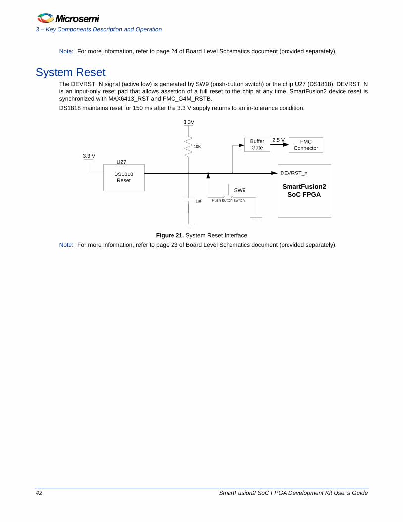
System Reset The DEVRST_N signal (active low) is generated by SW9 (push-button switch) or the chip U27 (DS1818). DEVRST_N is an input-only reset pad that allows assertion of a full reset to the chip at any time. SmartFusion2 device reset is synchronized with MAX6413_RST and FMC_G4M_RSTB. DS1818 maintains reset for 150 ms after the 3.3 V supply returns to an in-tolerance condition.
SmartFusion2 SoC FPGA
DEVRST_nDS1818Reset
10K
1uF
3.3V
Push button switch
3.3 V
SW9
Buffer Gate
FMC Connector
2.5 V
U27
Figure 21. System Reset Interface
Note: For more information, refer to page 23 of Board Level Schematics document (provided separately).

3 – Key Components Description and Operation
SmartFusion2 SoC FPGA Development Kit User’s Guide 43
Clock Oscillator A 50 MHz clock oscillator with +/-50 ppm is available on the board (Figure 20). This clock oscillator is connected to the FPGA fabric to provide a system reference clock. An on-chip SmartFusion2 PLL can be configured to generate a wide range of high precision clock frequencies.
Table 12. 50 MHz Clock SmartFusion2 Dev Kit SmartFusion2- Pkg No SmartFusion2 Pin Name
B7_50MHZ_U7 U7 MSIOD121PB7/CCC_SW0_CLKI0
Osc- 50MHz0
SmartFusion2 SoC FPGA
GND
TRISTATE VDD
OUT
1P8V
B7_50MHz_U7
Figure 22. Clock Oscillator Interface
Note: For more information, refer to page 26 of Board Level Schematics document (provided separately).
Debugging
User LEDs The board provides user access to eight active high LEDs, which are connected to the SmartFusion2 device for debugging applications.
Table 13. LEDs SmartFusion2 Dev Kit SmartFusion2 - Pkg No SmartFusion2 Pin Name
LED1 A18 DDRIO74PB0/MDDR_DQ16
LED2 B18 DDRIO74NB0/MDDR_DQ17
LED3 D18 DDRIO73PB0/MDDR_DQ18
LED4 E18 DDRIO73NB0/MDDR_DQ19
LED5 A20 DDRIO71NB0/MDDR_DQ20
LED6 D20 DDRIO70PB0/MDDR_DQ21
LED7 E20 DDRIO70NB0/MDDR_DQ22
LED8 B20 DDRIO69PB0/MDDR_DQ23
SmartFusion2 SoC FPGA
2 K
499
3.3 V
1 K
Figure 23. LEDs Interface
Note: For more information, refer to page 25 of Board Level Schematics document (provided separately).
3 – Key Components Description and Operation
44 SmartFusion2 SoC FPGA Development Kit User’s Guide
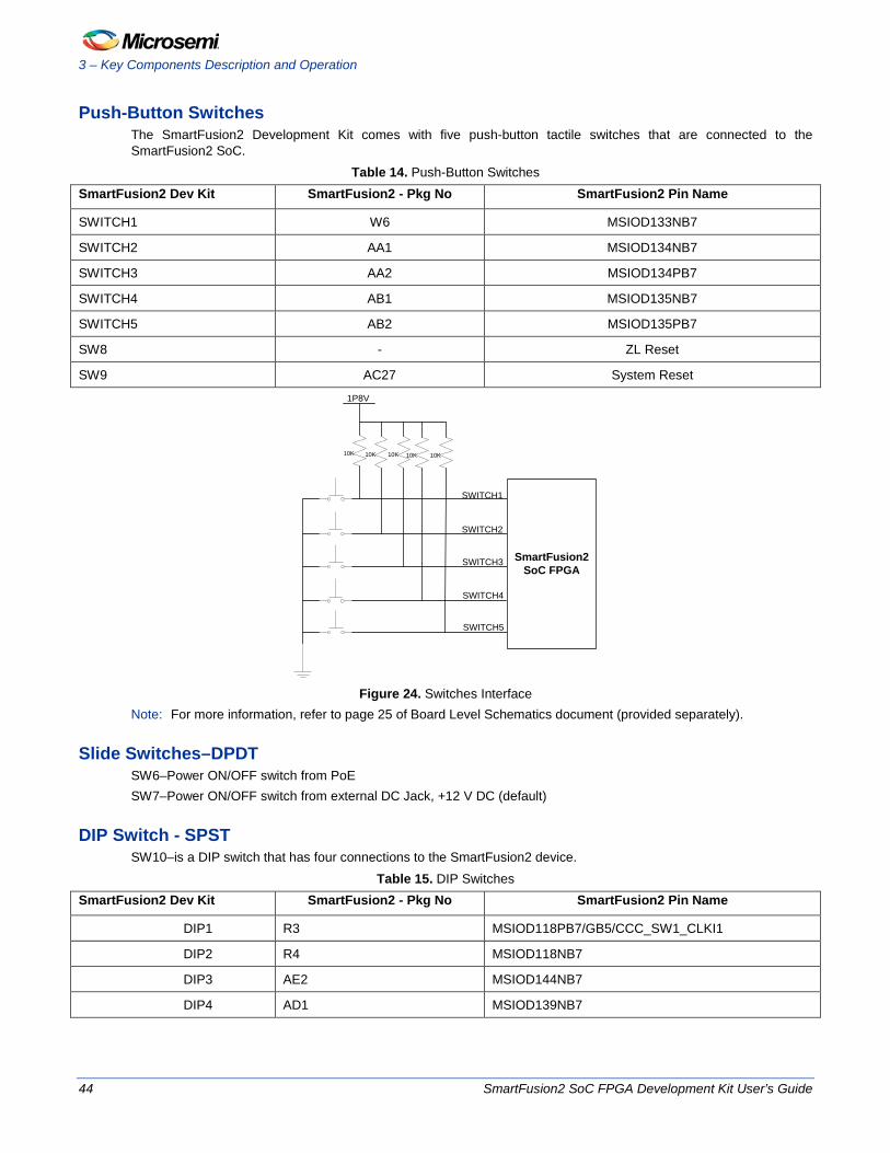
Push-Button Switches The SmartFusion2 Development Kit comes with five push-button tactile switches that are connected to the SmartFusion2 SoC.
Table 14. Push-Button Switches SmartFusion2 Dev Kit SmartFusion2 - Pkg No SmartFusion2 Pin Name
SWITCH1 W6 MSIOD133NB7
SWITCH2 AA1 MSIOD134NB7
SWITCH3 AA2 MSIOD134PB7
SWITCH4 AB1 MSIOD135NB7
SWITCH5 AB2 MSIOD135PB7
SW8 - ZL Reset
SW9 AC27 System Reset
SmartFusion2 SoC FPGA
SWITCH1
SWITCH2
SWITCH3
SWITCH4
SWITCH5
10K
1P8V
10K 10K 10K 10K
Figure 24. Switches Interface
Note: For more information, refer to page 25 of Board Level Schematics document (provided separately).
Slide Switches–DPDT SW6–Power ON/OFF switch from PoE SW7–Power ON/OFF switch from external DC Jack, +12 V DC (default)
DIP Switch - SPST SW10–is a DIP switch that has four connections to the SmartFusion2 device.
Table 15. DIP Switches SmartFusion2 Dev Kit SmartFusion2 - Pkg No SmartFusion2 Pin Name
DIP1 R3 MSIOD118PB7/GB5/CCC_SW1_CLKI1
DIP2 R4 MSIOD118NB7
DIP3 AE2 MSIOD144NB7
DIP4 AD1 MSIOD139NB7

3 – Key Components Description and Operation
SmartFusion2 SoC FPGA Development Kit User’s Guide 45
SmartFusion2 SoC FPGA
4.7K 4.7K 4.7K 4.7K
1P8V
DIP1
DIP2
DIP3
DIP4
SW10
1
Figure 25. SPST Interface Note: For more information, refer to page 25 of Board Level Schematics document (provided separately).
FMC Connector Pin Out The bank 0, bank 1, bank 2, bank 3, bank 5 (FDDR), and bank 6 (SERDES0) signals are routed to the FMC connector for user applications.
FMC Connector
SERDES0 SERDES0
Bank-5 FDDR
3.3V LT 2.5VSPI-0
3.3V LT 2.5VMSIOs
3.3V LT 2.5VMMUART0
3.3V LT 2.5VMMUART1
3.3V LT 2.5VCAN0
3.3V LT 2.5VI2C0
1.5V LT 2.5VDDRIOs
3.3V LT 2.5VI2C1
3.3V LT 2.5VSPI-1
2.5V
3.3V
SmartFusion2 SoC FPGA
Figure 26. FMC Connector

3 – Key Components Description and Operation
46 SmartFusion2 SoC FPGA Development Kit User’s Guide
Table 16. FMC Connector Pin out
FMC Connector – J3 SmartFusion2 – U42 Jumper
Pin No Row – A Pkg No Pin Name
1 GND
2 NC
3 NC
4 GND
5 GND
6 PCIE0_RXP_0 AB8 SERDES_0_RXD0_P
7 PCIE0_RXN_0 AB9 SERDES_0_RXD0_N
8 GND
9 GND
10 PCIE0_RXP_1 AC9 SERDES_0_RXD1_P
11 PCIE0_RXN_1 AC10 SERDES_0_RXD1_N
12 GND
13 GND
14 NC
15 NC
16 GND
17 GND
18 NC
19 NC
20 GND
21 GND
22 NC
23 NC
24 GND
25 GND
26 PCIE0_TXP_0 AJ2 SERDES_0_TXD0_P
27 PCIE0_TXN_0 AK2 SERDES_0_TXD0_N
28 GND
29 GND
30 PCIE0_TXP_1 AJ4 SERDES_0_TXD1_P
31 PCIE0_TXN_1 AK4 SERDES_0_TXD1_N
32 GND
33 GND
34 NC

3 – Key Components Description and Operation
SmartFusion2 SoC FPGA Development Kit User’s Guide 47
FMC Connector – J3 SmartFusion2 – U42 Jumper
Pin No Row – A Pkg No Pin Name
35 NC
36 GND
37 GND
38 NC
39 NC
40 GND
Pin No Row – B Pkg No Pin Name
1 NC
2 GND
3 GND
4 PCIE0_TXP_2 AJ6 SERDES_0_TXD2_P
5 PCIE0_TXN_2 AK6 SERDES_0_TXD2_N
6 GND
7 GND
8 PCIE0_TXP_3 AJ8 SERDES_0_TXD3_P
9 PCIE0_TXN_3 AK8 SERDES_0_TXD3_N
10 GND
11 GND
12 NC
13 NC
14 GND
15 GND
16 NC
17 NC
18 GND
19 GND
20 FMC_PCIE0_REFCLK0_P V9 MSIOD145PB6/SERDES_0_REFCLK0_P R159
21 FMC_PCIE0_REFCLK0_N V10 MSIOD145NB6/SERDES_0_REFCLK0_N R160
22 GND
23 GND
24 PCIE0_RXP_2 AB10 SERDES_0_RXD2_P
25 PCIE0_RXN_2 AB11 SERDES_0_RXD2_N
26 GND
27 GND
28 PCIE0_RXP_3 AD10 SERDES_0_RXD3_P

3 – Key Components Description and Operation
48 SmartFusion2 SoC FPGA Development Kit User’s Guide
FMC Connector – J3 SmartFusion2 – U42 Jumper
Pin No Row – B Pkg No Pin Name
29 PCIE0_RXN_3 AD11 SERDES_0_RXD3_N
30 GND
31 GND
32 NC
33 NC
34 GND
35 GND
36 NC
37 NC
38 GND
39 GND
40 NC
Pin No Row – C Pkg No Pin Name
1 GND
2 FMC_AK12_153_P AK12 DDRIO153PB5/FDDR_DQ0
3 FMC_AJ12_153_N AJ12 DDRIO153NB5/FDDR_DQ1
4 GND
5 GND
6 FMC_AK13_155_P AK13 DDRIO155PB5/FDDR_DQS0
7 FMC_AJ13_155_N AJ13 DDRIO155NB5/FDDR_DQS0_N
8 GND
9 GND
10 FMC_AF23_176_P AF23 DDRIO176PB5/FDDR_DQ30
11 FMC_AG23_176_N AG23 DDRIO176NB5/FDDR_DQ31
12 GND
13 GND
14 FMC_AJ14_158_P AJ14 DDRIO158PB5/FDDR_DQ7
15 FMC_AE14_158_N AE14 DDRIO158NB5/FDDR_TMATCH_OUT1
16 GND
17 GND
18 FMC_AE15_162_P AE15 DDRIO162PB5/FDDR_TMATCH_IN1
19 FMC_AG16_162_N AG16 DDRIO162NB5/FDDR_DM_RQDS1
20 GND
21 GND
22 FMC_AH27_183_P AH27 DDRIO183PB5/FDDR_ADDR1

3 – Key Components Description and Operation
SmartFusion2 SoC FPGA Development Kit User’s Guide 49
FMC Connector – J3 SmartFusion2 – U42 Jumper
Pin No Row – C Pkg No Pin Name
23 FMC_AJ27_183_N AJ27 DDRIO183NB5/FDDR_ADDR2
24 GND
25 GND
26 FMC_AE27_189_P AE27 DDRIO189PB5/FDDR_ADDR12
27 FMC_AF27_189_N AF27 DDRIO189NB5/FDDR_ADDR13
28 GND
29 GND
30 FMC_K24_2P5V K24 MSIO48NB1/I2C_0_SCL/GPIO_31_B/USB_DATA1_C J174
31 FMC_K23_2P5V K23 MSIO48PB1/I2C_0_SDA/GPIO_30_B/USB_DATA0_C J172
32 GND
33 GND
34 FMC_E21_2P5V E21 DDRIO67NB0/MDDR_DQ27
35 12P0V
36 GND
37 12P0V
38 GND
39 3P3V
40 GND
Pin No Row - D Pkg No Pin Name
1 FMC_AE11 AE11 DDRIO147PB5/FDDR_TMATCH_OUT_ECC
2 GND
3 GND
4 FMC_AK11_151_P AK11 DDRIO151PB5/FDDR_DQ_ECC0
5 FMC_AJ11_151_N AJ11 DDRIO151NB5/FDDR_DQ_ECC1
6 GND
7 GND
8 FMC_AG20_169_P AG20 DDRIO169PB5/FDDR_DQ21
9 FMC_AF20_169_N AF20 DDRIO169NB5/FDDR_DQ22
10 GND
11 FMC_AF11_152_P AF11 DDRIO152PB5/GB3/CCC_SW0_CLKI3/FDDR_DQ_ECC2
12 FMC_AG11_152_N AG11 DDRIO152NB5/GB7/CCC_SW1_CLKI2/FDDR_DQ_ECC3
13 GND
14 FMC_AG14_157_P AG14 DDRIO157PB5/FDDR_DQ5
15 FMC_AF14_157_N AF14 DDRIO157NB5/FDDR_DQ6
16 GND

3 – Key Components Description and Operation
50 SmartFusion2 SoC FPGA Development Kit User’s Guide
FMC Connector – J3 SmartFusion2 – U42 Jumper
Pin No Row - D Pkg No Pin Name
17 FMC_AK18_165_P AK18 DDRIO165PB5/FDDR_DQ16
18 FMC_AJ18_165_N AJ18 DDRIO165NB5/FDDR_DQ17
19 GND
20 FMC_AG21_172_P AG21 DDRIO172PB5/FDDR_DQ26
21 FMC_AF21_172_N AF21 DDRIO172NB5/FDDR_DQ27
22 GND
23 FMC_AK23_175_P AK23 DDRIO175PB5/FDDR_DQ28
24 FMC_AJ23_175_N AJ23 DDRIO175NB5/FDDR_DQ29
25 GND
26 FMC_AG27_187_P AG27 DDRIO187PB5/FDDR_ADDR8
27 FMC_AG28_187_N AG28 DDRIO187NB5/FDDR_ADDR9
28 GND
29 NC
30 NC
31 NC
32 3P3V
33 NC
34 NC
35 FMC_D22_2P5V D22 DDRIO65NB0/MDDR_DM_RQDS3
36 3P3V
37 GND
38 3P3V
39 GND
40 3P3V
Pin No Row – E Pkg No Pin Name
1 GND
2 FMC_AK10_149_P AK10 DDRIO149PB5/FDDR_DQS_ECC
3 FMC_AJ10_149_N AJ10 DDRIO149NB5/FDDR_DQS_ECC_N
4 GND
5 GND
6 FMC_L28_2P5V L28 MSIO34PB2/GPIO_3_B J155
7 FMC_L29_2P5V L29 MSIO33NB2/GPIO_2_B J146
8 GND
9 FMC_N25_2P5V N25 MSIO35PB2/GPIO_5_B J140
10 FMC_P23_2P5V P23 MSIO32PB2/GPIO_31_A J138

3 – Key Components Description and Operation
SmartFusion2 SoC FPGA Development Kit User’s Guide 51
FMC Connector – J3 SmartFusion2 – U42 Jumper
Pin No Row – E Pkg No Pin Name
11 GND
12 FMC_V24_2P5V V24 MSIO8PB3/CAN_RX/GPIO_3_A/USB_DATA1_A J111
13 FMC_R24_2P5V R24 MSIO24PB3/SPI_1_SS2/GPIO_15_A J133
14 GND
15 FMC_U24_2P5V U24 MSIO15PB3/SPI_0_SS6/GPIO_21_A J232
16 NC
17 GND
18 NC
19 NC
20 GND
21 FMC_U25_2P5V U25 MSIO19PB3/SPI_1_SS6/GPIO_23_A
22 FMC_U26_2P5V U26 MSIO15NB3/SPI_0_SS7/GPIO_22_A
23 GND
24 FMC_R25_2P5V R25 MSIO23PB3/SPI_0_SS3/GPIO_10_A/USB_DATA7_A
25 FMC_V22_2P5V V22 MSIO12PB3/SPI_0_CLK/USB_XCLK_A J110
26 GND
27 FMC_J29_2P5V J29 MSIO38PB1/MMUART_1_RTS/GPIO_11_B J184
28 FMC_W25_2P5V W25 MSIO4PB3/USB_DATA2_B
29 GND
30 FMC_E11_2P5V E11 DDRIO87PB0/CCC_NW1_CLKI3/MDDR_DQ_ECC2
31 FMC_D11_2P5V D11 DDRIO87NB0/MDDR_DQ_ECC3
32 GND
33 FMC_B21_2P5V B21 DDRIO68NB0/MDDR_DQ25
34 FMC_A21_2P5V A21 DDRIO68PB0/MDDR_DQ24
35 GND
36 FMC_A22_2P5V A22 DDRIO66NB0/MDDR_DQS3_N
37 FMC_E23_2P5V E23 DDRIO63PB0/MDDR_DQ30
38 GND
39 2P5V
40 GND
Pin No Row - F Pkg No Pin Name
1 FMC_G4M_RSTB
2 GND
3 GND

3 – Key Components Description and Operation
52 SmartFusion2 SoC FPGA Development Kit User’s Guide
FMC Connector – J3 SmartFusion2 – U42 Jumper
Pin No Row - F Pkg No Pin Name
4 FMC_K28_2P5V K28 MSIO34NB2/GPIO_4_B J161
5 FMC_K30_2P5V K30 MSIO37PB2/GPIO_9_B J159
6 GND
7 FMC_M26_2P5V M26 MSIO36NB2/GPIO_8_B J145
8 FMC_M27_2P5V M27 MSIO32NB2/GPIO_0_B J144
9 GND
10 FMC_P24_2P5V P24 MSIO31PB2/GPIO_29_A J139
11 FMC_T26_2P5V T26 MSIO21PB3/GPIO_27_A J134
12 GND
13 FMC_R29_2P5V R29 MSIO23NB3/SPI_1_SS1/GPIO_14_A J129
14 FMC_AA28_2P5V AA28 MSIO7NB3/CAN_TX/GPIO_2_A/USB_DATA0_AUU J114
15 GND
16 NC
17 NC
18 GND
19 FMC_W29_2P5V W29 MSIO14PB3/SPI_0_SS4/GPIO_19_A
20 FMC_R28_2P5V R28 MSIO24NB3/SPI_1_SS3/GPIO_16_A
21 GND
22 FMC_V29_2P5V V29 MSIO18PB3/SPI_1_SS4/GPIO_17_A
23 FMC_T30_2P5V T30 MSIO22PB3/SPI_0_SS1/GPIO_8_A/USB_DATA5_AUU
24 GND
25 FMC_W28_2P5V W28 MSIO13NB3/SPI_0_SS0/GPIO_7_A/USB_NXT_A J121
26 FMC_L26_2P5V L26 MSIO39NB1/MMUART_1_DSR/GPIO_14_B J175
27 GND
28 FMC_W27_2P5V W27 MSIO13PB3/SPI_0_SDO/GPIO_6_A/USB_STP_A J118
29 FMC_M23_2P5V M23 MSIO44PB1/MMUART_0_CTS/GPIO_19_B/USB_DATA7_C
J122
30 GND
31 FMC_A19_2P5V A19 DDRIO72PB0/MDDR_DQS2
32 FMC_B19_2P5V B19 DDRIO72NB0/MDDR_DQS2_N
33 GND
34 FMC_D21_2P5V D21 DDRIO67PB0/MDDR_DQ26
35 FMC_B22_2P5V B22 DDRIO66PB0/MDDR_DQS3
36 GND
37 FMC_D23_2P5V D23 DDRIO63NB0/MDDR_DQ31
3 – Key Components Description and Operation
SmartFusion2 SoC FPGA Development Kit User’s Guide 53
FMC Connector – J3 SmartFusion2 – U42 Jumper
Pin No Row - F Pkg No Pin Name
38 FMC_B23_2P5V B23 DDRIO64NB0/MDDR_DQ29
39 GND
40 2P5V
Pin No Row – G Pkg No Pin Name
1 GND
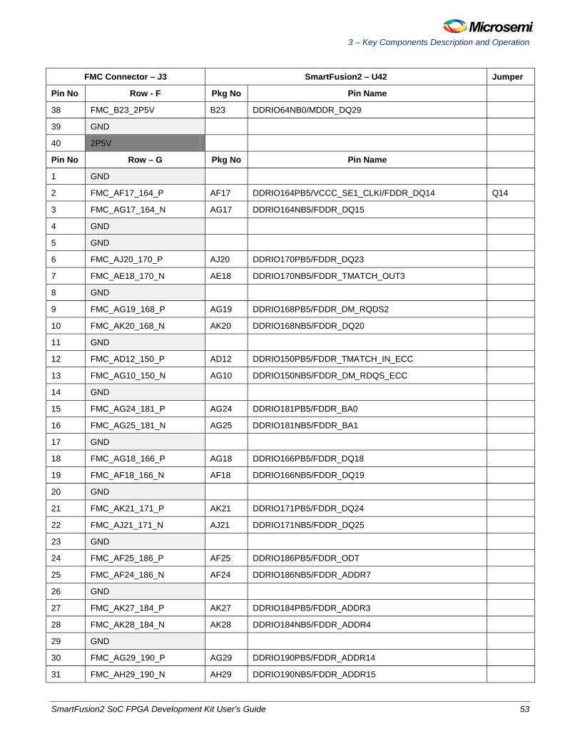
2 FMC_AF17_164_P AF17 DDRIO164PB5/VCCC_SE1_CLKI/FDDR_DQ14 Q14
3 FMC_AG17_164_N AG17 DDRIO164NB5/FDDR_DQ15
4 GND
5 GND
6 FMC_AJ20_170_P AJ20 DDRIO170PB5/FDDR_DQ23
7 FMC_AE18_170_N AE18 DDRIO170NB5/FDDR_TMATCH_OUT3
8 GND
9 FMC_AG19_168_P AG19 DDRIO168PB5/FDDR_DM_RQDS2
10 FMC_AK20_168_N AK20 DDRIO168NB5/FDDR_DQ20
11 GND
12 FMC_AD12_150_P AD12 DDRIO150PB5/FDDR_TMATCH_IN_ECC
13 FMC_AG10_150_N AG10 DDRIO150NB5/FDDR_DM_RDQS_ECC
14 GND
15 FMC_AG24_181_P AG24 DDRIO181PB5/FDDR_BA0
16 FMC_AG25_181_N AG25 DDRIO181NB5/FDDR_BA1
17 GND
18 FMC_AG18_166_P AG18 DDRIO166PB5/FDDR_DQ18
19 FMC_AF18_166_N AF18 DDRIO166NB5/FDDR_DQ19
20 GND
21 FMC_AK21_171_P AK21 DDRIO171PB5/FDDR_DQ24
22 FMC_AJ21_171_N AJ21 DDRIO171NB5/FDDR_DQ25
23 GND
24 FMC_AF25_186_P AF25 DDRIO186PB5/FDDR_ODT
25 FMC_AF24_186_N AF24 DDRIO186NB5/FDDR_ADDR7
26 GND
27 FMC_AK27_184_P AK27 DDRIO184PB5/FDDR_ADDR3
28 FMC_AK28_184_N AK28 DDRIO184NB5/FDDR_ADDR4
29 GND
30 FMC_AG29_190_P AG29 DDRIO190PB5/FDDR_ADDR14
31 FMC_AH29_190_N AH29 DDRIO190NB5/FDDR_ADDR15

3 – Key Components Description and Operation
54 SmartFusion2 SoC FPGA Development Kit User’s Guide
FMC Connector – J3 SmartFusion2 – U42 Jumper
Pin No Row – G Pkg No Pin Name
32 GND
33 FMC_AG30_177_P AG30 DDRIO177PB5/FDDR_RAS_N
34 FMC_AH30_177_N AH30 DDRIO177NB5/FDDR_WE_N
35 GND
36 FMC_AF29_178_P AF29 DDRIO178PB5/FDDR_CKE
37 FMC_AE29_178_N AE29 DDRIO178NB5/FDDR_CS_N
38 GND
39 2P5V
40 GND
Pin No Row - H Pkg No Pin Name
1 NC
2 FMC_J27_2P5V J27 MSIO35NB2/GPIO_6_B J162
3 GND
4 FMC_AK17_163_P AK17 DDRIO163PB5/GB15/VCCC_SE1_CLKI/FDDR_DQ12 Q12
5 FMC_AJ17_163_N AJ17 DDRIO163NB5/FDDR_DQ13
6 GND
7 FMC_AG13_156_P AG13 DDRIO156PB5/FDDR_DM_RQDS0
8 FMC_AK14_156_N AK14 DDRIO156NB5/FDDR_DQ4
9 GND
10 FMC_AE24_185_P AE24 DDRIO185PB5/FDDR_ADDR5
11 FMC_AE23_185_N AE23 DDRIO185NB5/FDDR_ADDR6
12 GND
13 FMC_AG12_154_P AG12 DDRIO154PB5/FDDR_DQ2
14 FMC_AF12_154_N AF12 DDRIO154NB5/FDDR_DQ3
15 GND
16 FMC_AG15_160_P AG15 DDRIO160PB5/VCCC_SE0_CLKI/FDDR_DQ10
17 FMC_AF15_160_N AF15 DDRIO160NB5/FDDR_DQ11
18 GND
19 FMC_AK19_167_P AK19 DDRIO167PB5/FDDR_DQS2
20 FMC_AJ19_167_N AJ19 DDRIO167NB5/FDDR_DQS2_N
21 GND
22 FMC_AE21_174_P AE21 DDRIO174PB5/FDDR_TMATCH_IN3
23 FMC_AG22_174_N AG22 DDRIO174NB5/FDDR_DM_RQDS3
24 GND
25 FMC_AK26_182_P AK26 DDRIO182PB5/FDDR_BA2

3 – Key Components Description and Operation
SmartFusion2 SoC FPGA Development Kit User’s Guide 55
FMC Connector – J3 SmartFusion2 – U42 Jumper
Pin No Row - H Pkg No Pin Name
26 FMC_AJ26_182_N AJ26 DDRIO182NB5/FDDR_ADDR0
27 GND
28 FMC_AJ29_188_P AJ29 DDRIO188PB5/FDDR_ADDR10
29 FMC_AJ28_188_N AJ28 DDRIO188NB5/FDDR_ADDR11
30 GND
31 FMC_AJ22_173_P AJ22 DDRIO173PB5/FDDR_DQS3
32 FMC_AK22_173_N AK22 DDRIO173NB5/FDDR_DQS3_N
33 GND
34 FMC_AK24_179_P AK24 DDRIO179PB5/FDDR_RST_N
35 FMC_AJ24_179_N AJ24 DDRIO179NB5/FDDR_CAS_N
36 GND
37 FMC_AK25_180_P AK25 DDRIO180PB5/FDDR_CLK
38 FMC_AJ25_180_N AJ25 DDRIO180NB5/FDDR_CLK_N
39 GND
40 2P5V
Pin No Row – J Pkg No Pin Name
1 GND
2 FMC_AK16_161_P AK16 DDRIO161PB5/GB11/VCCC_SE0_CLKI/FDDR_DQS1
3 FMC_AJ16_161_N AJ16 DDRIO161NB5/FDDR_DQS1_N
4 GND
5 GND
6 FMC_K29_2P5V K29 MSIO37NB2/GPIO_10_B J158
7 FMC_L30_2P5V L30 MSIO33PB2/GPIO_1_B J154
8 GND
9 FMC_T27_2P5V T27 MSIO21NB3/GPIO_28_A J131
10 FMC_AA29_2P5V AA29 MSIO8NB3/CAN_TX_EN_N/GPIO_4_A/USB_DATA2_A J115
11 GND
12 NC
13 NC
14 GND
15 NC
16 NC
17 GND
18 NC
19 NC

3 – Key Components Description and Operation
56 SmartFusion2 SoC FPGA Development Kit User’s Guide
FMC Connector – J3 SmartFusion2 – U42 Jumper
Pin No Row – J Pkg No Pin Name
20 GND
21 NC
22 NC
23 GND
24 FMC_W30_2P5V W30 MSIO14NB3/SPI_0_SS5/GPIO_20_A
25 FMC_H26_2P5V H26 MSIO47NB1/MMUART_0_CLK/GPIO_29_B/USB_NXT_C J179
26 GND
27 FMC_J30_2P5V J30 MSIO41PB1/GB10/VCCC_SE0_CLKI/USB_XCLK_C J183
28 FMC_H28_2P5V H28 MSIO40NB1/MMUART_1_DCD/GPIO_16_B J195
29 GND
30 FMC_F30_2P5V F30 MSIO45NB1/MMUART_0_DCD/GPIO_22_B J200
31 FMC_H29_2P5V H29 MSIO42PB1/GB14/VCCC_SE1_CLKI/MMUART_1_CLK/GPIO_25_B/USB_DATA4_C
J194
32 GND
33 FMC_D19_2P5V D19 DDRIO71PB0/MDDR_DM_RQDS2
34 FMC_H27_2P5V H27 MSI46NB1/MMUART_0_TXD/GPIO_27_B/USB_DIR_C J199
35 GND
36 FMC_N23_2P5V N23 MSIO39PB1/CCC_NE0_CLKI1/MMUART_1_CTS/GPIO_13_B
J214
37 FMC_V26_2P5V V26 MSIO11NB3/CCC_NE1_CLKI0/I2C_1_SCL/GPIO_1_A/USB_DATA4_A
J213
38 GND
39 2P5V
40 GND
Pin No Row - K Pkg No Pin Name
1 NC
2 GND
3 GND
4 FMC_AK15_159_P AK15 DDRIO159PB5/CCC_SW1_CLKI3/FDDR_DQ8
5 FMC_AJ15_159_N AJ15 DDRIO159NB5/FDDR_DQ9
6 GND
7 FMC_N24_2P5V N24 MSIO36PB2/GPIO_7_B J143
8 FMC_N26_2P5V N26 MSIO31NB2/GPIO_30_A J141
9 GND
10 FMC_Y30_2P5V Y30 MSIO12NB3/SPI_0_SDI/GPIO_5_A/USB_DIR_A J119
11 NC

3 – Key Components Description and Operation
SmartFusion2 SoC FPGA Development Kit User’s Guide 57
FMC Connector – J3 SmartFusion2 – U42 Jumper
Pin No Row - K Pkg No Pin Name
12 GND
13 NC
14 NC
15 GND
16 NC
17 NC
18 GND
19 NC
20 NC
21 GND
22 NC
23 FMC_V23_2P5V V23 MSIO11PB3/CCC_NE0_CLKI0/I2C_1_SDA/GPIO_0_A/USB_DATA3_A
J135
24 GND
25 FMC_J26_2P5V J26 MSIO43NB1/MMUART_0_DTR/GPIO_18_B/USB_DATA6_C
J178
26 FMC_H30_2P5V H30 MSIO41NB1/MMUART_1_TXD/GPIO_24_B/USB_DATA2_C
J188
27 GND
28 FMC_J28_2P5V J28 MSIO38NB1/MMUART_1_DTR/GPIO_12_B J187
29 FMC_G29_2P5V G29 MSIO42NB1/MMUART_1_RXD/GPIO_26_B/USB_DATA3_C
J197
30 GND
31 FMC_G30_2P5V G30 MSIO45PB1/MMUART_0_RI/GPIO_21_B J196
32 FMC_K25_2P5V K25 MSIO44NB1/MMUART_0_DSR/GPIO_20_B J202
33 GND
34 FMC_L23_2P5V L23 MSIO47PB1/MMUART_0_RXD/GPIO_28_B/USB_STP_C J210
35 FMC_M25_2P5V M25 MSIO40PB1/CCC_NE1_CLKI1/MMUART_1_RI/GPIO_15_B
J201
36 GND
37 FMC_M24_2P5V M24 MSIO43PB1/MMUART_0_RTS/GPIO_17_B/USB_DATA5_C
J209
38 FMC_A23_2P5V A23 DDRIO64PB0/MDDR_DQ28
39 GND
40 2P5V


SmartFusion2 SoC FPGA Development Kit User’s Guide 59
4 – Pin List
Pin list for SmartFusion2 M2S050T-FGG896 Devices.
Note: *H27- Pin cannot be used as a fabric output and it is only an Input. However, if it is coming from MSS UART as MMUART_0_TXD, it can be used as Output.
Table 17. Pin List M2S050T Pkg No Datasheet Pin Name LCP Pin Name Board Signal Name
A10 DDRIO90PB0/MDDR_DQS_ECC N1ADP0B90/MECCDQSP MDDR_CBS0_P
A11 DDRIO88PB0/MDDR_DQ_ECC0 N2ADP0B88/MECCD0 MDDR_CB0
A12 DDRIO86PB0/MDDR_DQ0 N3ADP0B86/M0D0 MDDR_DQ0
A13 DDRIO84PB0/MDDR_DQS0 N4ADP0B84/M0DQSP MDDR_DQS0_P
A14 DDRIO83NB0/MDDR_DQ4 N4DDN0B83/M0D4 MDDR_DQ4
A15 DDRIO80PB0/MDDR_DQ8 N6ADP0B80/M1D0 MDDR_DQ8
A16 DDRIO78PB0/GB8/CCC_NE0_CLKI3/MDDR_DQS1 N7ADP0B78/M1DQSP/GN5GC MDDR_DQS1_P
A17 DDRIO76PB0/GB12/CCC_NE1_CLKI2/MDDR_DQ12 N8ADP0B76/M1D4/GN6GC MDDR_DQ12
A18 DDRIO74PB0/MDDR_DQ16 N9ADP0B74/M2D0 LED1
A19 DDRIO72PB0/MDDR_DQS2 N10ADP0B72/M2DQSP FMC_A19_1P5V
A2 SERDES_1_TXD0_N N/PCIE1TXDN0 C_PCIE1_TXN_0
A20 DDRIO71NB0/MDDR_DQ20 N10DDN0B71/M2D4 LED5
A21 DDRIO68PB0/MDDR_DQ24 N12ADP0B68/M3D0 FMC_A21_1P5V
A22 DDRIO66NB0/MDDR_DQS3_N N13BDN0B66/M3DQSN FMC_A22_1P5V
A23 DDRIO64PB0/MDDR_DQ28 N14ADP0B64/M3D4 FMC_A23_1P5V
A24 DDRIO60PB0/MDDR_RST_N N16ADP0B60/MRSTN MDDR_RSTN
A25 DDRIO59PB0/MDDR_CLK N16CDP0B59/MRAMCLKP MDDR_CK_P
A26 DDRIO57PB0/MDDR_BA2 N17CDP0B57/MBS2 MDDR_BA2
A27 DDRIO55PB0/MDDR_ADDR3 N18CDP0B55/MADDR3 MDDR_A3
A28 DDRIO55NB0/MDDR_ADDR4 N18DDN0B55/MADDR4 MDDR_A4
A29 VSS VSS_5 GND
A3 VSS VSS_2 GND
A4 SERDES_1_TXD1_N N/PCIE1TXDN1 C_PCIE1_TXN_1
A5 VSS VSS_3 GND
A6 SERDES_1_TXD2_N N/PCIE1TXDN2 C_PCIE1_TXN_2
A7 VSS VSS_4 GND
A8 SERDES_1_TXD3_N N/PCIE1TXDN3 C_PCIE1_TXN_3
A9 DDRIO91PB0/GB0/CCC_NW0_CLKI3 N0CDP0B91//GN1GC Jumper J229
AA1 MSIOD134NB7 W8CFN7B134 SWITCH2

4 – Pin List
60 SmartFusion2 SoC FPGA Development Kit User’s Guide
M2S050T Pkg No Datasheet Pin Name LCP Pin Name Board Signal Name
AA10 CCC_SW0_PLL_VSSA PLL4VSSA PLL4VSSA
AA11 SERDES_0_L01_VDDAIO PCIE0VDDIOL PCIExVDDIOx
AA12 SERDES_0_L23_VDDAIO PCIE0VDDIOR PCIExVDDIOx
AA13 VDDI5 VDDI5_1 VDDIO5_2P5V
AA14 VDDI5 VDDI5_2 VDDIO5_2P5V
AA15 VDDI5 VDDI5_3 VDDIO5_2P5V
AA16 VDDI5 VDDI5_4 VDDIO5_2P5V
AA17 VDDI5 VDDI5_5 VDDIO5_2P5V
AA18 VDDI5 VDDI5_6 VDDIO5_2P5V
AA19 VDDI5 VDDI5_7 VDDIO5_2P5V
AA2 MSIOD134PB7 W8BFP7B134 SWITCH3
AA20 VDDI5 VDDI5_8 VDDIO5_2P5V
AA21 VDD VDD_1 VDD
AA22 VSS DMA Grounded
AA23 FDDR_PLL_VSSA PLLFDDRVSSA G4_PLLFDDRVSSA
AA24 VDDI4 VDDI4_1 VDDIO4_3P3V
AA25 JTAGSEL EMP4/JTAGSEL JTAG_SEL
AA26 MSIO2PB3/USB_STP_B E1BMP3B2/RGMIITXD1///UBSTP eMMC_DATA2
AA27 MSIO2NB3/USB_NXT_B E1CMN3B2/RGMIITXCTL///UBNXT eMMC_DATA1
AA28 MSIO7NB3/CAN_TX/GPIO_2_A/USB_DATA0_A E5AMN3B7/CANTXBUS//MI2A/UAD0 CANTXBUS1/FMC_AA28
AA29 MSIO8NB3/CAN_TX_EN_N/GPIO_4_A/USB_DATA2_A E5CMN3B8/CANTXEBL//MI4A/UAD2 CANTXEBL1/FMC_AA29
AA3 MSIOD129NB7 W12AFN7B129 SDRAM_A1
AA30 SC_SPI_CLK EMP3B9/G4CSSCK/OCITCK G4M_SPI_SCK
AA4 MSIOD136NB7 W7BFN7B136 SDRAM_DQ4_L0
AA5 MSIOD141NB7 W4AFN7B141 SDRAM_DQ6_L0
AA6 SERDES_0_L01_REXT PCIE0REXTL 1.21K resistor - PCIE0PLLREFRETL
AA7 SERDES_0_PLL_VSSA PLLPCIE0VSSA PLLPCIE0VSSA
AA8 SERDES_0_PLL_VDDA PLLPCIE0VDDA PLLPCIE0VDDA
AA9 SERDES_0_L23_REXT PCIE0REXTR 1.21K resistor - PCIE0PLLREFRETR
AB1 MSIOD135NB7 W8AFN7B135 SWITCH4
AB10 SERDES_0_RXD2_P S/PCIE0RXDP2 PCIE0_RXP_2
AB11 SERDES_0_RXD2_N S/PCIE0RXDN2 PCIE0_RXN_2
AB12 SERDES_0_VDD PCIE0VDD_2 PCIExVDD
AB13 VSS VSS_9 GND
AB14 VSS VSS_10 GND
AB15 VSS VSS_11 GND
AB16 VSS VSS_12 GND
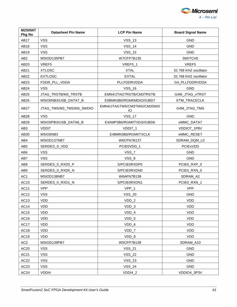
4 – Pin List
SmartFusion2 SoC FPGA Development Kit User’s Guide 61
M2S050T Pkg No Datasheet Pin Name LCP Pin Name Board Signal Name
AB17 VSS VSS_13 GND
AB18 VSS VSS_14 GND
AB19 VSS VSS_15 GND
AB2 MSIOD135PB7 W7CFP7B135 SWITCH5
AB20 VREF5 VREF5_1 VREF5
AB21 XTLOSC XTAL 32.768 KHZ oscillator
AB22 EXTLOSC EXTAL 32.768 KHZ oscillator
AB23 FDDR_PLL_VDDA PLLFDDRVDDA G4_PLLFDDRVDDA
AB24 VSS VSS_16 GND
AB25 JTAG_TRSTB/M3_TRSTB EMN4/JTAGTRSTB/CM3TRSTB G4M_JTAG_nTRST
AB26 MSIO0NB3/USB_DATA7_B E0BMN3B0/RGMIIMDIO///UBD7 ETM_TRACECLK
AB27 JTAG_TMS/M3_TMS/M3_SWDIO EMN4/JTAGTMS/CM3TMS//CM3SWDIO G4M_JTAG_TMS
AB28 VSS VSS_17 GND
AB29 MSIO6PB3/USB_DATA6_B E4AMP3B6/RGMIITXD3///UBD6 eMMC_DATA7
AB3 VDDI7 VDDI7_1 VDDIO7_1P8V
AB30 MSIO6NB3 E4BMN3B6/RGMIITXCLK eMMC_RESET
AB4 MSIOD137NB7 W6CFN7B137 SDRAM_DQM_L0
AB5 SERDES_0_VDD PCIE0VDD_1 PCIExVDD
AB6 VSS VSS_7 GND
AB7 VSS VSS_8 GND
AB8 SERDES_0_RXD0_P S/PCIE0RXDP0 PCIE0_RXP_0
AB9 SERDES_0_RXD0_N S/PCIE0RXDN0 PCIE0_RXN_0
AC1 MSIOD138NB7 W6AFN7B138 SDRAM_A2
AC10 SERDES_0_RXD1_N S/PCIE0RXDN1 PCIE0_RXN_1
AC11 VPP VPP_1 VPP
AC12 VSS VSS_20 GND
AC13 VDD VDD_2 VDD
AC14 VDD VDD_3 VDD
AC15 VDD VDD_4 VDD
AC16 VDD VDD_5 VDD
AC17 VDD VDD_6 VDD
AC18 VDD VDD_7 VDD
AC19 VDD VDD_8 VDD
AC2 MSIOD138PB7 W5CFP7B138 SDRAM_A10
AC20 VSS VSS_21 GND
AC21 VSS VSS_22 GND
AC22 VSS VSS_23 GND
AC23 VSS VSS_24 GND
AC24 VDDI4 VDDI4_2 VDDIO4_3P3V

4 – Pin List
62 SmartFusion2 SoC FPGA Development Kit User’s Guide
M2S050T Pkg No Datasheet Pin Name LCP Pin Name Board Signal Name
AC25 JTAG_TDO/M3_TDO/M3_SWO EMN4/JTAGTDO/CM3TDO//CM3SWO G4M_JTAG_TDO
AC26 JTAG_TCK/M3_TCK EMP4/JTAGTCK/CM3TCK G4M_JTAG_TCK
AC27 DEVRST_N DEVRSTB G4M_RSTB
AC28 MSIO1PB3/USB_XCLK_B E0CMP3B1/RGMIIGTXCLK///UBXCLK eMMC_DATA0
AC29 MSIO1NB3/USB_DIR_B E1AMN3B1/RGMIITXD0///UBDIR eMMC_DATA4
AC3 MSIOD140NB7 W4CFN7B140 SDRAM_DQ3_L0
AC30 MSIO5NB3/USB_DATA5_B E3CMN3B5/RGMIITXD2///UBD5 eMMC_DATA6
AC4 MSIOD143PB7 W2BFP7B143 SDRAM_DQ1_L0
AC5 VSS VSS_18 GND
AC6 VSS VSS_19 GND
AC7 SERDES_0_L01_VDDAPLL PCIE0VDDPLLL PCIE0VDDPLLL
AC8 SERDES_0_L01_REFRET PCIE0PLLREFRETL PCIE0PLLREFRETL
AC9 SERDES_0_RXD1_P S/PCIE0RXDP1 PCIE0_RXP_1
AD1 MSIOD139NB7 W5BFN7B139 DIP4
AD10 SERDES_0_RXD3_P S/PCIE0RXDP3 PCIE0_RXP_3
AD11 SERDES_0_RXD3_N S/PCIE0RXDN3 PCIE0_RXN_3
AD12 DDRIO150PB5/FDDR_TMATCH_IN_ECC S1CDP5B150/FECCFIFOWEIN FMC_AD12_150_P
AD13 VREF5 VREF5_2 VREF5
AD14 VSS VSS_30 GND
AD15 VSS VSS_31 GND
AD16 VREF5 VREF5_3 VREF5
AD17 VSS VSS_32 GND
AD18 VSS VSS_33 GND
AD19 VSS VSS_34 GND
AD2 MSIOD139PB7 W5AFP7B139 SDRAM_DQ5_L0
AD20 VSS VSS_35 GND
AD21 VSS VSS_36 GND
AD22 VSS VSS_37 GND
AD23 VSS VSS_38 GND
AD24 VSS VSS_39 GND
AD25 VSS VSS_40 GND
AD26 VSS VSS_41 GND
AD27 VSS VSS_42 GND
AD28 VSS VSS_43 GND
AD29 VSS VSS_44 GND
AD3 MSIOD143NB7 W2CFN7B143 SDRAM_DQ7_L0
AD30 MSIO5PB3/USB_DATA4_B E3BMP3B5/RGMIIRXD3///UBD4 eMMC_DATA5
AD4 VSS VSS_25 GND
AD5 VSS VSS_26 GND
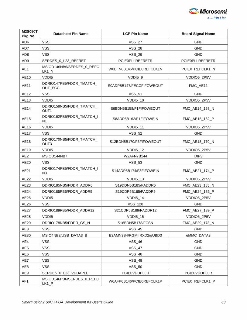
4 – Pin List
SmartFusion2 SoC FPGA Development Kit User’s Guide 63
M2S050T Pkg No Datasheet Pin Name LCP Pin Name Board Signal Name
AD6 VSS VSS_27 GND
AD7 VSS VSS_28 GND
AD8 VSS VSS_29 GND
AD9 SERDES_0_L23_REFRET PCIE0PLLREFRETR PCIE0PLLREFRETR
AE1 MSIOD146NB6/SERDES_0_REFCLK1_N W0BFN6B146/PCIE0REFCLK1N PCIE0_REFCLK1_N
AE10 VDDI5 VDDI5_9 VDDIO5_2P5V
AE11 DDRIO147PB5/FDDR_TMATCH_OUT_ECC S0ADP5B147/FECCFIFOWEOUT FMC_AE11
AE12 VSS VSS_51 GND
AE13 VDDI5 VDDI5_10 VDDIO5_2P5V
AE14 DDRIO158NB5/FDDR_TMATCH_OUT1 S6BDN5B158/F1FIFOWEOUT FMC_AE14_158_N
AE15 DDRIO162PB5/FDDR_TMATCH_IN1 S8ADP5B162/F1FIFOWEIN FMC_AE15_162_P
AE16 VDDI5 VDDI5_11 VDDIO5_2P5V
AE17 VSS VSS_52 GND
AE18 DDRIO170NB5/FDDR_TMATCH_OUT3 S12BDN5B170/F3FIFOWEOUT FMC_AE18_170_N
AE19 VDDI5 VDDI5_12 VDDIO5_2P5V
AE2 MSIOD144NB7 W2AFN7B144 DIP3
AE20 VSS VSS_53 GND
AE21 DDRIO174PB5/FDDR_TMATCH_IN3 S14ADP5B174/F3FIFOWEIN FMC_AE21_174_P
AE22 VDDI5 VDDI5_13 VDDIO5_2P5V
AE23 DDRIO185NB5/FDDR_ADDR6 S19DDN5B185/FADDR6 FMC_AE23_185_N
AE24 DDRIO185PB5/FDDR_ADDR5 S19CDP5B185/FADDR5 FMC_AE24_185_P
AE25 VDDI5 VDDI5_14 VDDIO5_2P5V
AE26 VSS VSS_128 GND
AE27 DDRIO189PB5/FDDR_ADDR12 S21CDP5B189/FADDR12 FMC_AE27_189_P
AE28 VDDI5 VDDI5_15 VDDIO5_2P5V
AE29 DDRIO178NB5/FDDR_CS_N S16BDN5B178/FCSN FMC_AE29_178_N
AE3 VSS VSS_45 GND
AE30 MSIO4NB3/USB_DATA3_B E3AMN3B4/RGMIIRXD2///UBD3 eMMC_DATA3
AE4 VSS VSS_46 GND
AE5 VSS VSS_47 GND
AE6 VSS VSS_48 GND
AE7 VSS VSS_49 GND
AE8 VSS VSS_50 GND
AE9 SERDES_0_L23_VDDAPLL PCIE0VDDPLLR PCIE0VDDPLLR
AF1 MSIOD146PB6/SERDES_0_REFCLK1_P W0AFP6B146/PCIE0REFCLK1P PCIE0_REFCLK1_P

4 – Pin List
64 SmartFusion2 SoC FPGA Development Kit User’s Guide
M2S050T Pkg No Datasheet Pin Name LCP Pin Name Board Signal Name
AF10 VDDI5 VDDI5_16 VDDIO5_2P5V
AF11 DDRIO152PB5/GB3/CCC_SW0_CLKI3/FDDR_DQ_ECC2 S2CDP5B152/FECCD2/GS1GC FMC_AF11_152_P
AF12 DDRIO154NB5/FDDR_DQ3 S3DDN5B154/F0D3 FMC_AF12_154_N
AF13 VDDI5 VDDI5_17 VDDIO5_2P5V
AF14 DDRIO157NB5/FDDR_DQ6 S5DDN5B157/F0D6 FMC_AF14_157_N
AF15 DDRIO160NB5/FDDR_DQ11 S7BDN5B160/F1D3 FMC_AF15_160_N
AF16 VDDI5 VDDI5_18 VDDIO5_2P5V
AF17 DDRIO164PB5/VCCC_SE1_CLKI/FDDR_DQ14 S9ADP5B164/F1D6/GS7V FMC_AF17_164_P
AF18 DDRIO166NB5/FDDR_DQ19 S10BDN5B166/F2D3 FMC_AF18_166_N
AF19 VDDI5 VDDI5_19 VDDIO5_2P5V
AF2 VSS VSS_54 GND
AF20 DDRIO169NB5/FDDR_DQ22 S11DDN5B169/F2D6 FMC_AF20_169_N
AF21 DDRIO172NB5/FDDR_DQ27 S13BDN5B172/F3D3 FMC_AF21_172_N
AF22 VDDI5 VDDI5_20 VDDIO5_2P5V
AF23 DDRIO176PB5/FDDR_DQ30 S15ADP5B176/F3D6 FMC_AF23_176_P
AF24 DDRIO186NB5/FDDR_ADDR7 S20BDN5B186/FADDR7 FMC_AF24_186_N
AF25 DDRIO186PB5/FDDR_ODT S20ADP5B186/FODT FMC_AF25_186_P
AF26 VSS VSS_61 GND
AF27 DDRIO189NB5/FDDR_ADDR13 S21DDN5B189/FADDR13 FMC_AF27_189_N
AF28 VDDI5 VDDI5_22 VDDIO5_2P5V
AF29 DDRIO178PB5/FDDR_CKE S16ADP5B178/FCKE FMC_AF29_178_P
AF3 VSS VSS_55 GND
AF30 VSS VSS_62 GND
AF4 VSS VSS_56 GND
AF5 VSS VSS_57 GND
AF6 VSS VSS_58 GND
AF7 VSS VSS_59 GND
AF8 VSS VSS_60 GND
AF9 FDDR_IMP_CALIB S5/FECCIMPCALIB Grounded
AG1 VSS VSS_63 GND
AG10 DDRIO150NB5/FDDR_DM_RDQS_ECC S1DDN5B150/FECCDM FMC_AG10_150_N
AG11 DDRIO152NB5/GB7/CCC_SW1_CLKI2/FDDR_DQ_ECC3 S2DDN5B152/FECCD3/GS2GC FMC_AG11_152_N
AG12 DDRIO154PB5/FDDR_DQ2 S3CDP5B154/F0D2 FMC_AG12_154_P
AG13 DDRIO156PB5/FDDR_DM_RQDS0 S4CDP5B156/F0DM FMC_AG13_156_P
AG14 DDRIO157PB5/FDDR_DQ5 S5CDP5B157/F0D5 FMC_AG14_157_P
AG15 DDRIO160PB5/VCCC_SE0_CLKI/FDDR_DQ10 S7ADP5B160/F1D2/GS4V FMC_AG15_160_P

4 – Pin List
SmartFusion2 SoC FPGA Development Kit User’s Guide 65
M2S050T Pkg No Datasheet Pin Name LCP Pin Name Board Signal Name
AG16 DDRIO162NB5/FDDR_DM_RQDS1 S8BDN5B162/F1DM FMC_AG16_162_N
AG17 DDRIO164NB5/FDDR_DQ15 S9BDN5B164/F1D7 FMC_AG17_164_N
AG18 DDRIO166PB5/FDDR_DQ18 S10ADP5B166/F2D2 FMC_AG18_166_P
AG19 DDRIO168PB5/FDDR_DM_RQDS2 S11ADP5B168/F2DM FMC_AG19_168_P
AG2 VSS VSS_64 GND
AG20 DDRIO169PB5/FDDR_DQ21 S11CDP5B169/F2D5 FMC_AG20_169_P
AG21 DDRIO172PB5/FDDR_DQ26 S13ADP5B172/F3D2 FMC_AG21_172_P
AG22 DDRIO174NB5/FDDR_DM_RQDS3 S14BDN5B174/F3DM FMC_AG22_174_N
AG23 DDRIO176NB5/FDDR_DQ31 S15BDN5B176/F3D7 FMC_AG23_176_N
AG24 DDRIO181PB5/FDDR_BA0 S17CDP5B181/FBS0 FMC_AG24_181_P
AG25 DDRIO181NB5/FDDR_BA1 S17DDN5B181/FBS1 FMC_AG25_181_N
AG26 VDDI5 VDDI5_21 VDDIO5_2P5V
AG27 DDRIO187PB5/FDDR_ADDR8 S20CDP5B187/FADDR8 FMC_AG27_187_P
AG28 DDRIO187NB5/FDDR_ADDR9 S20DDN5B187/FADDR9 FMC_AG28_187_N
AG29 DDRIO190PB5/FDDR_ADDR14 S22ADP5B190/FADDR14 FMC_AG29_190_P
AG3 VSS VSS_65 GND
AG30 DDRIO177PB5/FDDR_RAS_N S15CDP5B177/FRASN FMC_AG30_177_P
AG4 VSS VSS_66 GND
AG5 VSS VSS_67 GND
AG6 VSS VSS_68 GND
AG7 VSS VSS_69 GND
AG8 VSS VSS_70 GND
AG9 DDRIO147NB5/CCC_SW0_CLKI2 S0BDN5B147//GS0C S0BDN5B147_GS0C
AH1 VSS VSS_71 GND
AH10 VDDI5 VDDI5_23 VDDIO5_2P5V
AH11 VSS VSS_80 GND
AH12 VSS VSS_81 GND
AH13 VDDI5 VDDI5_24 VDDIO5_2P5V
AH14 VSS VSS_82 GND
AH15 VSS VSS_83 GND
AH16 VDDI5 VDDI5_25 VDDIO5_2P5V
AH17 VSS VSS_84 GND
AH18 VSS VSS_85 GND
AH19 VDDI5 VDDI5_26 VDDIO5_2P5V
AH2 VSS VSS_72 GND
AH20 VSS VSS_86 GND
AH21 VSS VSS_87 GND
AH22 VDDI5 VDDI5_27 VDDIO5_2P5V

4 – Pin List
66 SmartFusion2 SoC FPGA Development Kit User’s Guide
M2S050T Pkg No Datasheet Pin Name LCP Pin Name Board Signal Name
AH23 VSS VSS_88 GND
AH24 VSS VSS_89 GND
AH25 VDDI5 VDDI5_28 VDDIO5_2P5V
AH26 VSS VSS_90 GND
AH27 DDRIO183PB5/FDDR_ADDR1 S18CDP5B183/FADDR1 FMC_AH27_183_P
AH28 VDDI5 VDDI5_29 VDDIO5_2P5V
AH29 DDRIO190NB5/FDDR_ADDR15 S22BDN5B190/FADDR15 FMC_AH29_190_N
AH3 VSS VSS_73 GND
AH30 DDRIO177NB5/FDDR_WE_N S15DDN5B177/FWEN FMC_AH30_177_N
AH4 VSS VSS_74 GND
AH5 VSS VSS_75 GND
AH6 VSS VSS_76 GND
AH7 VSS VSS_77 GND
AH8 VSS VSS_78 GND
AH9 VSS VSS_79 GND
AJ1 VSS VSS_92 GND
AJ10 DDRIO149NB5/FDDR_DQS_ECC_N S1BDN5B149/FECCDQSN FMC_AJ10_149_N
AJ11 DDRIO151NB5/FDDR_DQ_ECC1 S2BDN5B151/FECCD1 FMC_AJ11_151_N
AJ12 DDRIO153NB5/FDDR_DQ1 S3BDN5B153/F0D1 FMC_AJ12_153_N
AJ13 DDRIO155NB5/FDDR_DQS0_N S4BDN5B155/F0DQSN FMC_AJ13_155_N
AJ14 DDRIO158PB5/FDDR_DQ7 S6ADP5B158/F0D7 FMC_AJ14_158_P
AJ15 DDRIO159NB5/FDDR_DQ9 S6DDN5B159/F1D1 FMC_AJ15_159_N
AJ16 DDRIO161NB5/FDDR_DQS1_N S7DDN5B161/F1DQSN FMC_AJ16_161_N
AJ17 DDRIO163NB5/FDDR_DQ13 S8DDN5B163/F1D5 FMC_AJ17_163_N
AJ18 DDRIO165NB5/FDDR_DQ17 S9DDN5B165/F2D1 FMC_AJ18_165_N
AJ19 DDRIO167NB5/FDDR_DQS2_N S10DDN5B167/F2DQSN FMC_AJ19_167_N
AJ2 SERDES_0_TXD0_P S/PCIE0TXDP0 C_PCIE0_TXP_0
AJ20 DDRIO170PB5/FDDR_DQ23 S12ADP5B170/F2D7 FMC_AJ20_170_P
AJ21 DDRIO171NB5/FDDR_DQ25 S12DDN5B171/F3D1 FMC_AJ21_171_N
AJ22 DDRIO173PB5/FDDR_DQS3 S13CDP5B173/F3DQSP FMC_AJ22_173_P
AJ23 DDRIO175NB5/FDDR_DQ29 S14DDN5B175/F3D5 FMC_AJ23_175_N
AJ24 DDRIO179NB5/FDDR_CAS_N S16DDN5B179/FCASN FMC_AJ24_179_N
AJ25 DDRIO180NB5/FDDR_CLK_N S17BDN5B180/FRAMCLKN FMC_AJ25_180_N
AJ26 DDRIO182NB5/FDDR_ADDR0 S18BDN5B182/FADDR0 FMC_AJ26_182_N
AJ27 DDRIO183NB5/FDDR_ADDR2 S18DDN5B183/FADDR2 FMC_AJ27_183_N
AJ28 DDRIO188NB5/FDDR_ADDR11 S21BDN5B188/FADDR11 FMC_AJ28_188_N
AJ29 DDRIO188PB5/FDDR_ADDR10 S21ADP5B188/FADDR10 FMC_AJ29_188_P
AJ3 VSS VSS_93 GND
AJ30 VSS VSS_96 GND

4 – Pin List
SmartFusion2 SoC FPGA Development Kit User’s Guide 67
M2S050T Pkg No Datasheet Pin Name LCP Pin Name Board Signal Name
AJ4 SERDES_0_TXD1_P S/PCIE0TXDP1 C_PCIE0_TXP_1
AJ5 VSS VSS_94 GND
AJ6 SERDES_0_TXD2_P S/PCIE0TXDP2 C_PCIE0_TXP_2
AJ7 VSS VSS_95 GND
AJ8 SERDES_0_TXD3_P S/PCIE0TXDP3 C_PCIE0_TXP_3
AJ9 DDRIO148NB5/PROBE_B S0DDN5B148//PRB PRB
AK10 DDRIO149PB5/FDDR_DQS_ECC S1ADP5B149/FECCDQSP FMC_AK10_149_P
AK11 DDRIO151PB5/FDDR_DQ_ECC0 S2ADP5B151/FECCD0 FMC_AK11_151_P
AK12 DDRIO153PB5/FDDR_DQ0 S3ADP5B153/F0D0 FMC_AK12_153_P
AK13 DDRIO155PB5/FDDR_DQS0 S4ADP5B155/F0DQSP FMC_AK13_155_P
AK14 DDRIO156NB5/FDDR_DQ4 S4DDN5B156/F0D4 FMC_AK14_156_N
AK15 DDRIO159PB5/CCC_SW1_CLKI3/FDDR_DQ8 S6CDP5B159/F1D0/GS3C FMC_AK15_159_P
AK16 DDRIO161PB5/GB11/VCCC_SE0_CLKI/FDDR_DQS1 S7CDP5B161/F1DQSP/GS5GV FMC_AK16_161_P
AK17 DDRIO163PB5/GB15/VCCC_SE1_CLKI/FDDR_DQ12 S8CDP5B163/F1D4/GS6GV FMC_AK17_163_P
AK18 DDRIO165PB5/FDDR_DQ16 S9CDP5B165/F2D0 FMC_AK18_165_P
AK19 DDRIO167PB5/FDDR_DQS2 S10CDP5B167/F2DQSP FMC_AK19_167_P
AK2 SERDES_0_TXD0_N S/PCIE0TXDN0 C_PCIE0_TXN_0
AK20 DDRIO168NB5/FDDR_DQ20 S11BDN5B168/F2D4 FMC_AK20_168_N
AK21 DDRIO171PB5/FDDR_DQ24 S12CDP5B171/F3D0 FMC_AK21_171_P
AK22 DDRIO173NB5/FDDR_DQS3_N S13DDN5B173/F3DQSN FMC_AK22_173_N
AK23 DDRIO175PB5/FDDR_DQ28 S14CDP5B175/F3D4 FMC_AK23_175_P
AK24 DDRIO179PB5/FDDR_RST_N S16CDP5B179/FRSTN FMC_AK24_179_P
AK25 DDRIO180PB5/FDDR_CLK S17ADP5B180/FRAMCLKP FMC_AK25_180_P
AK26 DDRIO182PB5/FDDR_BA2 S18ADP5B182/FBS2 FMC_AK26_182_P
AK27 DDRIO184PB5/FDDR_ADDR3 S19ADP5B184/FADDR3 FMC_AK27_184_P
AK28 DDRIO184NB5/FDDR_ADDR4 S19BDN5B184/FADDR4 FMC_AK28_184_N
AK29 VSS VSS_101 GND
AK3 VSS VSS_98 GND
AK4 SERDES_0_TXD1_N S/PCIE0TXDN1 C_PCIE0_TXN_1
AK5 VSS VSS_99 GND
AK6 SERDES_0_TXD2_N S/PCIE0TXDN2 C_PCIE0_TXN_2
AK7 VSS VSS_100 GND
AK8 SERDES_0_TXD3_N S/PCIE0TXDN3 C_PCIE0_TXN_3
AK9 DDRIO148PB5/PROBE_A S0CDP5B148//PRA PRA
B1 VSS VSS_103 GND
B10 DDRIO90NB0/MDDR_DQS_ECC_N N1BDN0B90/MECCDQSN MDDR_CBS0_N
B11 DDRIO88NB0/MDDR_DQ_ECC1 N2BDN0B88/MECCD1 MDDR_CB1

4 – Pin List
68 SmartFusion2 SoC FPGA Development Kit User’s Guide
M2S050T Pkg No Datasheet Pin Name LCP Pin Name Board Signal Name
B12 DDRIO86NB0/MDDR_DQ1 N3BDN0B86/M0D1 MDDR_DQ1
B13 DDRIO84NB0/MDDR_DQS0_N N4BDN0B84/M0DQSN MDDR_DQS0_N
B14 DDRIO81PB0/MDDR_DQ7 N5CDP0B81/M0D7 MDDR_DQ7
B15 DDRIO80NB0/MDDR_DQ9 N6BDN0B80/M1D1 MDDR_DQ9
B16 DDRIO78NB0/MDDR_DQS1_N N7BDN0B78/M1DQSN MDDR_DQS1_N
B17 DDRIO76NB0/MDDR_DQ13 N8BDN0B76/M1D5 MDDR_DQ13
B18 DDRIO74NB0/MDDR_DQ17 N9BDN0B74/M2D1 LED2
B19 DDRIO72NB0/MDDR_DQS2_N N10BDN0B72/M2DQSN FMC_B19_1P5V
B2 SERDES_1_TXD0_P N/PCIE1TXDP0 C_PCIE1_TXP_0
B20 DDRIO69PB0/MDDR_DQ23 N11CDP0B69/M2D7 LED8
B21 DDRIO68NB0/MDDR_DQ25 N12BDN0B68/M3D1 FMC_B21_1P5V
B22 DDRIO66PB0/MDDR_DQS3 N13ADP0B66/M3DQSP FMC_B22_1P5V
B23 DDRIO64NB0/MDDR_DQ29 N14BDN0B64/M3D5 FMC_B23_1P5V
B24 DDRIO60NB0/MDDR_CAS_N N16BDN0B60/MCASN MDDR_CAS_L
B25 DDRIO59NB0/MDDR_CLK_N N16DDN0B59/MRAMCLKN MDDR_CK_N
B26 DDRIO57NB0/MDDR_ADDR0 N17DDN0B57/MADDR0 MDDR_A0
B27 DDRIO56NB0/MDDR_ADDR2 N18BDN0B56/MADDR2 MDDR_A2
B28 DDRIO51NB0/MDDR_ADDR11 N20DDN0B51/MADDR11 MDDR_A11
B29 DDRIO51PB0/MDDR_ADDR10 N20CDP0B51/MADDR10 MDDR_A10
B3 VSS VSS_104 GND
B30 VSS VSS_107 GND
B4 SERDES_1_TXD1_P N/PCIE1TXDP1 C_PCIE1_TXP_1
B5 VSS VSS_105 GND
B6 SERDES_1_TXD2_P N/PCIE1TXDP2 C_PCIE1_TXP_2
B7 VSS VSS_106 GND
B8 SERDES_1_TXD3_P N/PCIE1TXDP3 C_PCIE1_TXP_3
B9 DDRIO91NB0/GB4/CCC_NW1_CLKI2 N0DDN0B91//GN2GC N0DDN0B91_GN2GC
C1 VSS VSS_108 GND
C10 VDDI0 VDDI0_1 VDDIO0_1P5V
C11 VSS VSS_117 GND
C12 VSS VSS_118 GND
C13 VDDI0 VDDI0_2 VDDIO0_1P5V
C14 VSS VSS_119 GND
C15 VSS VSS_120 GND
C16 VDDI0 VDDI0_3 VDDIO0_1P5V
C17 VSS VSS_121 GND
C18 VSS VSS_122 GND
C19 VDDI0 VDDI0_4 VDDIO0_1P5V
C2 VSS VSS_109 GND

4 – Pin List
SmartFusion2 SoC FPGA Development Kit User’s Guide 69
M2S050T Pkg No Datasheet Pin Name LCP Pin Name Board Signal Name
C20 VSS VSS_123 GND
C21 VSS VSS_124 GND
C22 VDDI0 VDDI0_5 VDDIO0_1P5V
C23 VSS VSS_125 GND
C24 VSS VSS_126 GND
C25 VDDI0 VDDI0_6 VDDIO0_1P5V
C26 VSS VSS_127 GND
C27 DDRIO56PB0/MDDR_ADDR1 N18ADP0B56/MADDR1 MDDR_A1
C28 VDDI0 VDDI0_7 VDDIO0_1P5V
C29 DDRIO49NB0/MDDR_ADDR15 N21DDN0B49/MADDR15 MDDR_A15
C3 VSS VSS_110 GND
C30 DDRIO62NB0/MDDR_WE_N N15BDN0B62/MWEN MDDR_WE_L
C4 VSS VSS_111 GND
C5 VSS VSS_112 GND
C6 VSS VSS_113 GND
C7 VSS VSS_114 GND
C8 VSS VSS_115 GND
C9 VSS VSS_116 GND
D1 VSS VSS_129 GND
D10 DDRIO89NB0/MDDR_DM_RDQS_ECC N1DDN0B89/MECCDM MDDR_CBM
D11 DDRIO87NB0/MDDR_DQ_ECC3 N2DDN0B87/MECCD3 FMC_D11_1P5V
D12 DDRIO85PB0/MDDR_DQ2 N3CDP0B85/M0D2 MDDR_DQ2
D13 DDRIO83PB0/MDDR_DM_RQDS0 N4CDP0B83/M0DM MDDR_DQM0
D14 DDRIO82PB0/MDDR_DQ5 N5ADP0B82/M0D5 MDDR_DQ5
D15 DDRIO79PB0/CCC_NE0_CLKI2/MDDR_DQ10 N6CDP0B79/M1D2/GN4C MDDR_DQ10
D16 DDRIO77NB0/MDDR_DM_RQDS1 N7DDN0B77/M1DM MDDR_DQM1
D17 DDRIO75NB0/MDDR_DQ15 N8DDN0B75/M1D7 MDDR_DQ15
D18 DDRIO73PB0/MDDR_DQ18 N9CDP0B73/M2D2 LED3
D19 DDRIO71PB0/MDDR_DM_RQDS2 N10CDP0B71/M2DM FMC_D19_1P5V
D2 VSS VSS_130 GND
D20 DDRIO70PB0/MDDR_DQ21 N11ADP0B70/M2D5 LED6
D21 DDRIO67PB0/MDDR_DQ26 N12CDP0B67/M3D2 FMC_D21_1P5V
D22 DDRIO65NB0/MDDR_DM_RQDS3 N13DDN0B65/M3DM FMC_D22_1P5V
D23 DDRIO63NB0/MDDR_DQ31 N14DDN0B63/M3D7 FMC_D23_1P5V
D24 DDRIO58PB0/MDDR_BA0 N17ADP0B58/MBS0 MDDR_BA0
D25 DDRIO58NB0/MDDR_BA1 N17BDN0B58/MBS1 MDDR_BA1
D26 VDDI0 VDDI0_13 VDDIO0_1P5V
D27 DDRIO52PB0/MDDR_ADDR8 N20ADP0B52/MADDR8 MDDR_A8
D28 DDRIO52NB0/MDDR_ADDR9 N20BDN0B52/MADDR9 MDDR_A9

4 – Pin List
70 SmartFusion2 SoC FPGA Development Kit User’s Guide
M2S050T Pkg No Datasheet Pin Name LCP Pin Name Board Signal Name
D29 DDRIO49PB0/MDDR_ADDR14 N21CDP0B49/MADDR14 MDDR_A14
D3 VSS VSS_131 GND
D30 DDRIO62PB0/MDDR_RAS_N N15ADP0B62/MRASN MDDR_RAS_L
D4 VSS VSS_132 GND
D5 VSS VSS_133 GND
D6 VSS VSS_134 GND
D7 VSS VSS_135 GND
D8 VSS VSS_136 GND
D9 DDRIO92NB0/CCC_NW0_CLKI2 N0BDN0B92//GN0C Jumper J228
E1 MSIOD94NB9/SERDES_1_REFCLK1_N W35CFN9B94/PCIE1REFCLK0N PCIE1_REFCLK0_N
E10 VDDI0 VDDI0_8 VDDIO0_1P5V
E11 DDRIO87PB0/CCC_NW1_CLKI3/MDDR_DQ_ECC2 N2CDP0B87/MECCD2/GN3C FMC_E11_1P5V
E12 DDRIO85NB0/MDDR_DQ3 N3DDN0B85/M0D3 MDDR_DQ3
E13 VDDI0 VDDI0_9 VDDIO0_1P5V
E14 DDRIO82NB0/MDDR_DQ6 N5BDN0B82/M0D6 MDDR_DQ6
E15 DDRIO79NB0/MDDR_DQ11 N6DDN0B79/M1D3 MDDR_DQ11
E16 VDDI0 VDDI0_10 VDDIO0_1P5V
E17 DDRIO75PB0/CCC_NE1_CLKI3/MDDR_DQ14 N8CDP0B75/M1D6/GN7C MDDR_DQ14
E18 DDRIO73NB0/MDDR_DQ19 N9DDN0B73/M2D3 LED4
E19 VDDI0 VDDI0_11 VDDIO0_1P5V
E2 VSS VSS_137 GND
E20 DDRIO70NB0/MDDR_DQ22 N11BDN0B70/M2D6 LED7
E21 DDRIO67NB0/MDDR_DQ27 N12DDN0B67/M3D3 FMC_E21_1P5V
E22 VDDI0 VDDI0_12 VDDIO0_1P5V
E23 DDRIO63PB0/MDDR_DQ30 N14CDP0B63/M3D6 FMC_E23_1P5V
E24 DDRIO53NB0/MDDR_ADDR7 N19DDN0B53/MADDR7 MDDR_A7
E25 DDRIO53PB0/MDDR_ODT N19CDP0B53/MODT MDDR_ODT
E26 VSS VSS_144 GND
E27 DDRIO50NB0/MDDR_ADDR13 N21BDN0B50/MADDR13 MDDR_A13
E28 VDDI0 VDDI0_14 VDDIO0_1P5V
E29 DDRIO61PB0/MDDR_CKE N15CDP0B61/MCKE MDDR_CKE
E3 VSS VSS_138 GND
E30 VSS VSS_145 GND
E4 VSS VSS_139 GND
E5 VSS VSS_140 GND
E6 VSS VSS_141 GND
E7 VSS VSS_142 GND
E8 VSS VSS_143 GND

4 – Pin List
SmartFusion2 SoC FPGA Development Kit User’s Guide 71
M2S050T Pkg No Datasheet Pin Name LCP Pin Name Board Signal Name
E9 MDDR_IMP_CALIB N0/MECCIMPCALIB Grounded
F1 MSIOD94PB9/SERDES_1_REFCLK1_P W35BFP9B94/PCIE1REFCLK0P PCIE1_REFCLK0_P
F10 VDDI0 VDDI0_15 VDDIO0_1P5V
F11 DDRIO92PB0/MDDR_TMATCH_OUT_ECC N0ADP0B92/MECCFIFOWEOUT G12
F12 VSS VSS_152 GND
F13 VDDI0 VDDI0_16 VDDIO0_1P5V
F14 DDRIO81NB0/MDDR_TMATCH_OUT1 N5DDN0B81/M1FIFOWEOUT F15
F15 DDRIO77PB0/MDDR_TMATCH_IN1 N7CDP0B77/M1FIFOWEIN F14
F16 VDDI0 VDDI0_17 VDDIO0_1P5V
F17 VSS VSS_153 GND
F18 DDRIO69NB0/MDDR_TMATCH_OUT3 N11DDN0B69/M3FIFOWEOUT F21
F19 VDDI0 VDDI0_18 VDDIO0_1P5V
F2 MSIO108NB8 W26AMN8B108 TS_TXD6
F20 VSS VSS_154 GND
F21 DDRIO65PB0/MDDR_TMATCH_IN3 N13CDP0B65/M3FIFOWEIN F18
F22 VDDI0 VDDI0_19 VDDIO0_1P5V
F23 DDRIO54NB0/MDDR_ADDR6 N19BDN0B54/MADDR6 MDDR_A6
F24 DDRIO54PB0/MDDR_ADDR5 N19ADP0B54/MADDR5 MDDR_A5
F25 VSS VSS_91 GND
F26 VDDI0 VDDI0_20 VDDIO0_1P5V
F27 DDRIO50PB0/MDDR_ADDR12 N21ADP0B50/MADDR12 MDDR_A12
F28 VDDI0 VDDI0_21 VDDIO0_1P5V
F29 DDRIO61NB0/MDDR_CS_N N15DDN0B61/MCSN MDDR_CS_L
F3 VSS VSS_146 GND
F30 MSIO45NB1/MMUART_0_DCD/GPIO_22_B E29BMN1B45/M0DCD//MI22B ADS8568_DB11/FMC_F30
F4 VSS VSS_147 GND
F5 VSS VSS_148 GND
F6 VSS VSS_149 GND
F7 VSS VSS_150 GND
F8 VSS VSS_151 GND
F9 SERDES_1_L23_VDDAPLL PCIE1VDDPLLR PCIE1VDDPLLR
G1 MSIO100NB8 W31BMN8B100 TS_TXD0
G10 SERDES_1_RXD3_P N/PCIE1RXDP3 R_RXP_3
G11 SERDES_1_RXD3_N N/PCIE1RXDN3 R_RXN_3
G12 DDRIO89PB0/MDDR_TMATCH_IN_ECC N1CDP0B89/MECCFIFOWEIN F11

4 – Pin List
72 SmartFusion2 SoC FPGA Development Kit User’s Guide
M2S050T Pkg No Datasheet Pin Name LCP Pin Name Board Signal Name
G13 VREF0 VREF0_1 VREF0
G14 VSS VSS_160 GND
G15 VSS VSS_161 GND
G16 VREF0 VREF0_2 VREF0
G17 VSS VSS_162 GND
G18 VSS VSS_163 GND
G19 VSS VSS_164 GND
G2 MSIO95PB8 W34BMP8B95 TS_TXD1
G20 VSS VSS_165 GND
G21 VSS VSS_166 GND
G22 VSS VSS_167 GND
G23 VSS VSS_168 GND
G24 VSS VSS_169 GND
G25 VSS VSS_170 GND
G26 VSS VSS_171 GND
G27 VSS VSS_172 GND
G28 FLASH_GOLDEN_N EMP1B46/MANFREFLASH/OCIRSTB G4M_SPI_REFLASH
G29 MSIO42NB1/MMUART_1_RXD/GPIO_26_B/USB_DATA3_C E27BMN1B42/M1RXD//MI26B/UCD3 RS232_ROUT/FMC_G29
G3 MSIO95NB8 W34CMN8B95 TS_TXD2
G30 MSIO45PB1/MMUART_0_RI/GPIO_21_B E29AMP1B45/M0RI//MI21B ADS8568_DB8/FMC_G30
G4 VSS VSS_155 GND
G5 VSS VSS_156 GND
G6 VSS VSS_157 GND
G7 VSS VSS_158 GND
G8 VSS VSS_159 GND
G9 SERDES_1_L23_REFRET PCIE1PLLREFRETR PCIE1PLLREFRETR
H1 MSIO99PB8 W31CMP8B99 TS_REFCLK
H10 SERDES_1_RXD1_N N/PCIE1RXDN1 R_RXN_1
H11 VSS VSS_175 GND
H12 VSS VSS_176 GND
H13 VDD VDD_9 VDD
H14 VDD VDD_10 VDD
H15 VDD VDD_11 VDD
H16 VDD VDD_12 VDD
H17 VDD VDD_13 CORE_SENSE+
H18 VDD VDD_14 VDD
H19 VDD VDD_15 VDD
H2 MSIO99NB8 W32AMN8B99 POF_SPI_CSN
H20 VSS VSS_177 GND

4 – Pin List
SmartFusion2 SoC FPGA Development Kit User’s Guide 73
M2S050T Pkg No Datasheet Pin Name LCP Pin Name Board Signal Name
H21 VSS VSS_178 GND
H22 VSS VSS_179 GND
H23 VSS VSS_180 GND
H24 CCC_NE0_PLL_VDDA PLL0VDDA PLL0VDDA
H25 CCC_NE0_PLL_VSSA PLL0VSSA PLL0VSSA
H26 MSIO47NB1/MMUART_0_CLK/GPIO_29_B/USB_NXT_C E30BMN1B47/M0SCK//MI29B/UCNXT ADS8568_REFEN/FMC_H26
H27* MSI46NB1/MMUART_0_TXD/GPIO_27_B/USB_DIR_C E29CMN1B46/M0TXD//MI27B/UCDIR RS485_TX/FMC_H27
H28 MSIO40NB1/MMUART_1_DCD/GPIO_16_B E26AMN1B40/M1DCD//MI16B RS232_INVALIDn/FMC_H28
H29 MSIO42PB1/GB14/VCCC_SE1_CLKI/MMUART_1_CLK/GPIO_25_B/USB_DATA4_C
E27AMP1B42/M1SCK//MI25B/UCD4/GE7GV ADS8568_DB3/FMC_H29
H3 VDDI8 VDDI8_1 VDDIO8_3P3V
H30 MSIO41NB1/MMUART_1_TXD/GPIO_24_B/USB_DATA2_C E26CMN1B41/M1TXD//MI24B/UCD2 RS232_DIN/FMC_H30
H4 MSIO96NB8 W34AMN8B96 TS_TXCLK
H5 VSS VSS_173 GND
H6 VSS VSS_174 GND
H7 SERDES_1_L01_VDDAPLL PCIE1VDDPLLL PCIE1VDDPLLL
H8 SERDES_1_L01_REFRET PCIE1PLLREFRETL PCIE1PLLREFRETL
H9 SERDES_1_RXD1_P N/PCIE1RXDP1 R_RXP_1
J1 MSIO102PB8 W29CMP8B102
J10 SERDES_1_RXD2_P N/PCIE1RXDP2 R_RXP_2
J11 SERDES_1_RXD2_N N/PCIE1RXDN2 R_RXN_2
J12 SERDES_1_VDD PCIE1VDD_1 PCIExVDD
J13 VSS VSS_184 GND
J14 VSS VSS_185 GND
J15 VSS VSS_186 GND
J16 VSS VSS_187 GND
J17 VSS VSS_188 GND
J18 VSS VSS_189 GND
J19 VSS VSS_190 GND
J2 MSIO102NB8 W30AMN8B102 TS_RXD0
J20 VREF0 VREF0_3 VREF0
J21 VSS VSS_191 GND
J22 MDDR_PLL_VDDA PLLMDDRVDDA G4_PLLMDDRVDDA
J23 MDDR_PLL_VSSA PLLMDDRVSSA G4_PLLMDDRVSSA
J24 CCC_NE1_PLL_VSSA PLL1VSSA PLL1VSSA
J25 CCC_NE1_PLL_VDDA PLL1VDDA PLL1VDDA
J26 MSIO43NB1/MMUART_0_DTR/GP E28AMN1B43/M0DTR//MI18B/UCD6 RS485_RE/FMC_J26

4 – Pin List
74 SmartFusion2 SoC FPGA Development Kit User’s Guide
M2S050T Pkg No Datasheet Pin Name LCP Pin Name Board Signal Name
IO_18_B/USB_DATA6_C
J27 MSIO35NB2/GPIO_6_B E22CMN2B35///MI6B ADS8568_SEL_B/FMC_J27
J28 MSIO38NB1/MMUART_1_DTR/GPIO_12_B E24CMN1B38/M1DTR//MI12B ADS8568_SDO_D/FMC_J28
J29 MSIO38PB1/MMUART_1_RTS/GPIO_11_B E24BMP1B38/M1RTS//MI11B ADS8568_SDO_C/FMC_J29
J3 MSIO98PB8 W32BMP8B98 TS_MDC
J30 MSIO41PB1/GB10/VCCC_SE0_CLKI/USB_XCLK_C E26BMP1B41////UCXCLK/GE6GV ADS8568_DB2/FMC_J30
J4 MSIO98NB8 W32CMN8B98 TS_TXD3
J5 VSS VSS_181 GND
J6 VSS VSS_182 GND
J7 VSS VSS_183 GND
J8 SERDES_1_RXD0_P N/PCIE1RXDP0 R_RXP_0
J9 SERDES_1_RXD0_N N/PCIE1RXDN0 R_RXN_0
K1 VSS VSS_192 GND
K10 CCC_NW1_PLL_VDDA PLL3VDDA PLL3VDDA
K11 SERDES_1_L01_VDDAIO PCIE1VDDIOL PCIExVDDIOx
K12 SERDES_1_L23_VDDAIO PCIE1VDDIOR PCIExVDDIOx
K13 VDDI0 VDDI0_22 VDDIO0_1P5V
K14 VDDI0 VDDI0_23 VDDIO0_1P5V
K15 VDDI0 VDDI0_24 VDDIO0_1P5V
K16 VDDI0 VDDI0_25 VDDIO0_1P5V
K17 VDDI0 VDDI0_26 VDDIO0_1P5V
K18 VDDI0 VDDI0_27 VDDIO0_1P5V
K19 VDDI0 VDDI0_28 VDDIO0_1P5V
K2 VDDI8 VDDI8_2 VDDIO8_3P3V
K20 VDDI0 VDDI0_29 VDDIO0_1P5V
K21 VDD VDD_16 VDD
K22 VSS VSS_194 GND
K23 MSIO48PB1/I2C_0_SDA/GPIO_30_B/USB_DATA0_C E30CMP1B48/I2C0SDA//MI30B/UCD0 J172
K24 MSIO48NB1/I2C_0_SCL/GPIO_31_B/USB_DATA1_C E31AMN1B48/I2C0SCL//MI31B/UCD1 J174
K25 MSIO44NB1/MMUART_0_DSR/GPIO_20_B E28CMN1B44/M0DSR//MI20B ADS8568_DB7/FMC_K25
K26 VDDI1 VDDI1_1 VDDIO1_3P3V
K27 VSS VSS_195 GND
K28 MSIO34NB2/GPIO_4_B E22AMN2B34///MI4B ADS8568_RESET/FMC_K28
K29 MSIO37NB2/GPIO_10_B E24AMN2B37///MI10B ADS8568_SDO_B/FMC_K29
K3 MSIO101NB8 W30CMN8B101 TS_RXD3
K30 MSIO37PB2/GPIO_9_B E23CMP2B37///MI9B ADS8568_SDO_A/FMC_K30

4 – Pin List
SmartFusion2 SoC FPGA Development Kit User’s Guide 75
M2S050T Pkg No Datasheet Pin Name LCP Pin Name Board Signal Name
K4 VSS VSS_193 GND
K5 MSIO97NB8 W33BMN8B97 TS_RXD2
K6 SERDES_1_L01_REXT PCIE1REXTL PCIE1PLLREFRETL
K7 SERDES_1_PLL_VSSA PLLPCIE1VSSA PLLPCIE1VSSA
K8 SERDES_1_PLL_VDDA PLLPCIE1VDDA PLLPCIE1VDDA
K9 SERDES_1_L23_REXT PCIE1REXTR PCIE1PLLREFRETR
L1 MSIO104NB8 W28CMN8B104 TS_RXD6
L10 CCC_NW1_PLL_VSSA PLL3VSSA PLL3VSSA
L11 VSS VSS_197 GND
L12 VSS VSS_198 GND
L13 VSS VSS_199 GND
L14 VSS VSS_200 GND
L15 VSS VSS_201 GND
L16 VSS VSS_202 GND
L17 VSS VSS_203 GND
L18 VSS VSS_204 GND
L19 VSS VSS_205 GND
L2 MSIO103PB8 W29AMP8B103 TS_RXD5
L20 VSS VSS_206 GND
L21 VDDI1 VDDI1_2 VDDIO1_3P3V
L22 VDD VDD_17 VDD
L23 MSIO47PB1/MMUART_0_RXD/GPIO_28_B/USB_STP_C E30AMP1B47/M0RXD//MI28B/UCSTP RS485_RX/FMC_L23
L24 VSS VSS_207 GND
L25 VDDI1 VDDI1_3 VDDIO1_3P3V
L26 MSIO39NB1/MMUART_1_DSR/GPIO_14_B E25BMN1B39/M1DSR//MI14B ADS8568_DB0/FMC_L26
L27 VDDI2 VDDI2_1 VDDIO2_3P3V
L28 MSIO34PB2/GPIO_3_B E21CMP2B34///MI3B ADS8568_CONVST_D/FMC_L28
L29 MSIO33NB2/GPIO_2_B E21BMN2B33///MI2B ADS8568_CONVST_C/FMC_L29
L3 MSIO103NB8 W29BMN8B103 TS_RXD4
L30 MSIO33PB2/GPIO_1_B E21AMP2B33///MI1B ADS8568_CONVST_B/FMC_L30
L4 MSIO113NB8 W22CMN8B113 TS_TXD4
L5 VSS VSS_196 GND
L6 MSIOD93PB9/SERDES_1_REFCLK0_P W36AFP9B93/PCIE1REFCLK1P PCIE1_REFCLK1_P
L7 MSIOD93NB9/SERDES_1_REFCLK0_N W36BFN9B93/PCIE1REFCLK1N PCIE1_REFCLK1_N
L8 SERDES_1_VDD PCIE1VDD_2 PCIExVDD

4 – Pin List
76 SmartFusion2 SoC FPGA Development Kit User’s Guide
M2S050T Pkg No Datasheet Pin Name LCP Pin Name Board Signal Name
L9 CCC_NW0_PLL_VSSA PLL2VSSA PLL2VSSA
M1 MSIO107PB8 W26BMP8B107 TS_RX_ER
M10 VDD VDD_18 VDD
M11 VSS VSS_208 GND
M12 VSS VSS_209 GND
M13 VSS VSS_210 GND
M14 VSS VSS_211 GND
M15 VSS VSS_212 GND
M16 VSS VSS_213 GND
M17 VSS VSS_214 GND
M18 VSS VSS_215 GND
M19 VSS VSS_216 GND
M2 MSIO107NB8 W26CMN8B107 TS_RX_DV
M20 VSS VSS_217 GND
M21 VSS VSS_218 GND
M22 VSS VSS_219 GND
M23 MSIO44PB1/MMUART_0_CTS/GPIO_19_B/USB_DATA7_C E28BMP1B44/M0CTS//MI19B/UCD7 ADS8568_DB4/FMC_M23
M24 MSIO43PB1/MMUART_0_RTS/GPIO_17_B/USB_DATA5_C E27CMP1B43/M0RTS//MI17B/UCD5 RS485_TE/FMC_M24
M25 MSIO40PB1/CCC_NE1_CLKI1/MMUART_1_RI/GPIO_15_B E25CMP1B40/M1RI//MI15B//GE5C ADS8568_DB1/FMC_M25
M26 MSIO36NB2/GPIO_8_B E23BMN2B36///MI8B ADS8568_SCLK/FMC_M26
M27 MSIO32NB2/GPIO_0_B E20CMN2B32///MI0B ADS8568_CONVST_A/FMC_M27
M28 MSIO30NB2/USB_DATA7_D/GPIO_23_B E19BMN2B30/UDD7//MI23B USB_DATA7
M29 VSS VSS_220 GND
M3 MSIO106PB8 W27AMP8B106 TS_RXD7
M30 MSIO29NB2/USB_DATA5_D E18CMN2B29/UDD5 USB_DATA5
M4 MSIO106NB8 W27BMN8B106 TS_TXD7
M5 MSIO105NB8 W28AMN8B105 TS_COL
M6 VDDI8 VDDI8_3 VDDIO8_3P3V
M7 VDDI9 VDDI9 VDDIO9_2P5V
M8 MSIO97PB8 W33AMP8B97 TS_CRS
M9 CCC_NW0_PLL_VDDA PLL2VDDA PLL2VDDA
N1 MSIO111PB8 W23CMP8B111 G4M_ZL_RST
N10 VDDI8 VDDI8_4 VDDIO8_3P3V
N11 VSS VSS_221 GND
N12 VSS VSS_222 GND
N13 VSS VSS_223 GND
N14 VSS VSS_224 GND

4 – Pin List
SmartFusion2 SoC FPGA Development Kit User’s Guide 77
M2S050T Pkg No Datasheet Pin Name LCP Pin Name Board Signal Name
N15 VSS VSS_225 GND
N16 VSS VSS_226 GND
N17 VSS VSS_227 GND
N18 VSS VSS_228 GND
N19 VSS VSS_229 GND
N2 MSIO111NB8 W24AMN8B111 SFP_TX_DISABLE
N20 VSS VSS_230 GND
N21 VDDI1 VDDI1_4 VDDIO1_3P3V
N22 VDD VDD_19 VDD
N23 MSIO39PB1/CCC_NE0_CLKI1/MMUART_1_CTS/GPIO_13_B E25AMP1B39/M1CTS//MI13B//GE4C ADS8568_RDn/FMC_N23
N24 MSIO36PB2/GPIO_7_B E23AMP2B36///MI7B ADS8568_SDI/FMC_N24
N25 MSIO35PB2/GPIO_5_B E22BMP2B35///MI5B ADS8568_SEL_CD/FMC_N25
N26 MSIO31NB2/GPIO_30_A E20AMN2B31///MI30A ADS8568_CSn/FMC_N26
N27 MSIO30PB2/USB_DATA6_D E19AMP2B30/UDD6 USB_DATA6
N28 MSIO29PB2/USB_DATA4_D E18BMP2B29/UDD4 USB_DATA4
N29 MSIO28NB2/USB_DATA3_D E18AMN2B28/UDD3 USB_DATA3
N3 MSIO110PB8 W24BMP8B110 PHY_INTN
N30 MSIO26NB2/USB_NXT_D E16CMN2B26/UDNXT USB_NXT
N4 MSIO110NB8 W24CMN8B110 PHY_RST
N5 MSIO109NB8 W25BMN8B109 PHY_MDC
N6 MSIO100PB8 W31AMP8B100 TS_TXD5
N7 MSIO96PB8 W33CMP8B96 TS_RXCLK
N8 MSIO101PB8 W30BMP8B101 SFP_LOS
N9 MSIO104PB8 W28BMP8B104 TS_GTXCLK
P1 MSIO115PB8/GB2/CCC_NW0_CLKI1 W21AMP8B115//GW6GC TSEC1_TX_CLK+
P10 VDD VDD_20 VDD
P11 VSS VSS_231 GND
P12 VSS VSS_232 GND
P13 VSS VSS_233 GND
P14 VSS VSS_234 GND
P15 VSS VSS_235 GND
P16 VSS VSS_236 GND
P17 VSS VSS_237 GND
P18 VSS VSS_238 GND
P19 VSS VSS_239 GND
P2 MSIO115NB8 W21BMN8B115 TSEC1_TX_CLK-
P20 VSS VSS_240 GND
P21 VDDI2 VDDI2_2 VDDIO2_3P3V
P22 VSS VSS_241 GND

4 – Pin List
78 SmartFusion2 SoC FPGA Development Kit User’s Guide
M2S050T Pkg No Datasheet Pin Name LCP Pin Name Board Signal Name
P23 MSIO32PB2/GPIO_31_A E20BMP2B32///MI31A ADS8568_BUSY_INT/FMC_P23
P24 MSIO31PB2/GPIO_29_A E19CMP2B31///MI29A USB_RESET/FMC_P24
P25 MSIO28PB2/USB_DATA2_D E17CMP2B28/UDD2 USB_DATA2
P26 MSIO27PB2/USB_DATA0_D E17AMP2B27/UDD0 USB_DATA0
P27 MSIO27NB2/USB_DATA1_D E17BMN2B27/UDD1 USB_DATA1
P28 MSIO26PB2/USB_STP_D E16BMP2B26/UDSTP USB_STP
P29 MSIO25NB2/USB_DIR_D E16AMN2B25/UDDIR USB_DIR
P3 MSIO114PB8/GB6/CCC_NW1_CLKI1 W21CMP8B114//GW7GC G4M SyncE
P30 MSIO25PB2/USB_XCLK_D E15CMP2B25/UDXCLK USB_CLKOUT
P4 MSIO114NB8 W22AMN8B114 TS_TX_ER
P5 MSIO112NB8 W23BMN8B112 SF2_PHY__CONFIG1
P6 MSIO105PB8 W27CMP8B105 TS_TX_EN
P7 MSIO108PB8 W25CMP8B108 TS_RST_N
P8 MSIO112PB8 W23AMP8B112 TS_MDIO
P9 MSIO116PB8/CCC_NW1_CLKI0 W20BMP8B116//GW5C G4M_RCVRD_CLK1
R1 MSIOD119PB7/GB1/CCC_SW0_CLKI1 W18BFP7B119//GW2GC unused
R10 VDDI8 VDDI8_5 VDDIO8_3P3V
R11 VSS VSS_242 GND
R12 VSS VSS_243 GND
R13 VSS VSS_244 GND
R14 VSS VSS_245 GND
R15 VSS VSS_246 GND
R16 VSS VSS_247 GND
R17 VSS VSS_248 GND
R18 VSS VSS_249 GND
R19 VSS VSS_250 GND
R2 MSIOD119NB7 W18CFN7B119 unused
R20 VSS VSS_251 GND
R21 VDDI2 VDDI2_3 VDDIO2_3P3V
R22 VDD VDD_21 VDD
R23 VPP VPP_2 VPP
R24 MSIO24PB3/SPI_1_SS2/GPIO_15_A E14CMP3B24/S1SS2//MI15A FMC_R24_3P3V / FT4232_DD1
R25 MSIO23PB3/SPI_0_SS3/GPIO_10_A/USB_DATA7_A E14AMP3B23/S0SS3//MI10A/UAD7 FMC_R25_3P3V
R26 VDDI2 VDDI2_4 VDDIO2_3P3V
R27 VSS VSS_252 GND
R28 MSIO24NB3/SPI_1_SS3/GPIO_16_A E15AMN3B24/S1SS3//MI16A FMC_R28_3P3V
R29 MSIO23NB3/SPI_1_SS1/GPIO_14 E14BMN3B23/S1SS1//MI14A FMC_R29_3P3V / FT4232_DD0

4 – Pin List
SmartFusion2 SoC FPGA Development Kit User’s Guide 79
M2S050T Pkg No Datasheet Pin Name LCP Pin Name Board Signal Name
_A
R3 MSIOD118PB7/GB5/CCC_SW1_CLKI1 W19AFP7B118//GW3GC DIP1
R30 MSIO22NB3/SPI_0_SS2/GPIO_9_A/USB_DATA6_A E13CMN3B22/S0SS2//MI9A/UAD6 PCIE1_PERSTn
R4 MSIOD118NB7 W19BFN7B118 DIP2
R5 MSIO116NB8 W20CMN8B116 POF_SPI_SCK
R6 MSIO117NB8 W20AMN8B117 POF_SPI_MOSI
R7 MSIO109PB8 W25AMP8B109 PHY_MDIO
R8 MSIO113PB8 W22BMP8B113 POF_SPI_MISO
R9 MSIO117PB8/CCC_NW0_CLKI0 W19CMP8B117//GW4C G4M_RCVRD_CLK2
T1 MSIOD120NB7 W18AFN7B120 SDRAM_A12
T10 VDD VDD_22 VDD
T11 VSS VSS_254 GND
T12 VSS VSS_255 GND
T13 VSS VSS_256 GND
T14 VSS VSS_257 GND
T15 VSS VSS_258 GND
T16 VSS VSS_259 GND
T17 VSS VSS_260 GND
T18 VSS VSS_261 GND
T19 VSS VSS_262 GND
T2 VSS VSS_253 GND
T20 VSS VSS_263 GND
T21 VSS VSS_264 GND
T22 VSS VSS_265 GND
T23 VSSNVM VSSNVMSA0 Grounded
T24 MSIO20PB3/GB9/VCCC_SE0_CLKI/GPIO_25_A E12AMP3B20///MI25A//GE2GV HPCLKOUT6_SPARE_PTP_CL
K
T25 VDDI3 VDDI3_1 VDDIO3_3P3V
T26 MSIO21PB3/GPIO_27_A E12CMP3B21///MI27A CANRXBUS2/FMC_T26
T27 MSIO21NB3/GPIO_28_A E13AMN3B21///MI28A CANTXEBL2/FMC_T27
T28 MSIO20NB3/GB13/VCCC_SE1_CLKI/GPIO_26_A E12BMN3B20///MI26A//GE3GV 1588_G4M_TRIG
T29 VPPNVM VPPNVMSA0 VPPNVMSA0
T3 VDDI7 VDDI7_2 VDDIO7_1P8V
T30 MSIO22PB3/SPI_0_SS1/GPIO_8_A/USB_DATA5_A E13BMP3B22/S0SS1//MI8A/UAD5 FMC_T30_3P3V
T4 MSIOD121NB7 W17BFN7B121 unused
T5 MSIOD125NB7 W14CFN7B125 SDRAM_A7
T6 MSIOD128PB7 W12BFP7B128 SDRAM_A8
T7 MSIOD120PB7/CCC_SW1_CLKI0 W17CFP7B120//GW1C SDRAM_DQ0_U0

4 – Pin List
80 SmartFusion2 SoC FPGA Development Kit User’s Guide
M2S050T Pkg No Datasheet Pin Name LCP Pin Name Board Signal Name
T8 MSIOD124PB7 W15AFP7B124 SDRAM_DQM_U0
T9 MSIOD133PB7 W9AFP7B133 SFP_SDA
U1 MSIOD122NB7 W16CFN7B122 SDRAM_A5
U10 VDDI7 VDDI7_3 VDDIO7_1P8V
U11 VSS VSS_266 GND
U12 VSS VSS_267 GND
U13 VSS VSS_268 GND
U14 VSS VSS_269 GND
U15 VSS VSS_270 GND
U16 VSS VSS_271 GND
U17 VSS VSS_272 GND
U18 VSS VSS_273 GND
U19 VSS VSS_274 GND
U2 MSIOD122PB7 W16BFP7B122 SDRAM_A9
U20 VSS VSS_275 GND
U21 VDDI3 VDDI3_2 VDDIO3_3P3V
U22 VDD VDD_23 VDD
U23 MSIO16PB3/SPI_1_CLK E9BMP3B16/S1SCK G4M_ZL_SCL
U24 MSIO15PB3/SPI_0_SS6/GPIO_21_A E8CMP3B15/S0SS6//MI21A CANTXBUS2/FMC_U24
U25 MSIO19PB3/SPI_1_SS6/GPIO_23_A E11BMP3B19/S1SS6//MI23A FMC_U25_3P3V
U26 MSIO15NB3/SPI_0_SS7/GPIO_22_A E9AMN3B15/S0SS7//MI22A FMC_U26_3P3V
U27 MSIO16NB3/SPI_1_SDI/GPIO_11_A E9CMN3B16/S1SDI//MI11A G4M_ZL_SI
U28 VDDI3 VDDI3_3 VDDIO3_3P3V
U29 VSS VSS_276 GND
U3 MSIOD123NB7 W16AFN7B123 SDRAM_CKE
U30 MSIO19NB3/SPI_1_SS7/GPIO_24_A E11CMN3B19/S1SS7//MI24A eMMC_CMD
U4 MSIOD123PB7 W15CFP7B123 SDRAM_CLK
U5 MSIOD124NB7 W15BFN7B124 SDRAM_A11
U6 MSIOD136PB7 W7AFP7B136 SFP_SCL
U7 MSIOD121PB7/CCC_SW0_CLKI0 W17AFP7B121//GW0C B7_50MHZ_U7
U8 MSIOD125PB7 W14BFP7B125 SDRAM_DQ4_U0
U9 MSIOD132PB7 W9CFP7B132 SDRAM_DQ2_U0
V1 MSIOD127PB7 W13AFP7B127 SDRAM_A6
V10 MSIOD145NB6/SERDES_0_REFCLK0_N W1AFN6B145/PCIE0REFCLK0N PCIE0_REFCLK0_N
V11 VSS VSS_277 GND
V12 VSS VSS_278 GND

4 – Pin List
SmartFusion2 SoC FPGA Development Kit User’s Guide 81
M2S050T Pkg No Datasheet Pin Name LCP Pin Name Board Signal Name
V13 VSS VSS_279 GND
V14 VSS VSS_280 GND
V15 VSS VSS_281 GND
V16 VSS VSS_282 GND
V17 VSS VSS_283 GND
V18 VSS VSS_284 GND
V19 VSS VSS_285 GND
V2 MSIOD127NB7 W13BFN7B127 SDRAM_A4
V20 VSS VSS_286 GND
V21 VSS VSS_287 GND
V22 MSIO12PB3/SPI_0_CLK/USB_XCLK_A E6CMP3B12/S0SCK///UAXCLK SPI0_SCK/FMC_V22
V23 MSIO11PB3/CCC_NE0_CLKI0/I2C_1_SDA/GPIO_0_A/USB_DATA3_A
E6AMP3B11/I2C1SDA//MI0A/UAD3/GE0C 3P3V / FMC_V23_3P3V
V24 MSIO8PB3/CAN_RX/GPIO_3_A/USB_DATA1_A E5BMP3B8/CANRXBUS//MI3A/UAD1 CANRXBUS1/FMC_V24
V25 VPP VPP_3 VPP
V26 MSIO11NB3/CCC_NE1_CLKI0/I2C_1_SCL/GPIO_1_A/USB_DATA4_A
E6BMN3B11/I2C1SCL//MI1A/UAD4/GE1C I2C1SCL/FMC_V26
V27 MSIO17PB3/SPI_1_SDO/GPIO_12_A E10AMP3B17/S1SDO//MI12A G4M_ZL_SO
V28 MSIO17NB3/SPI_1_SS0/GPIO_13_A E10BMN3B17/S1SS0//MI13A G4M_ZL_CS
V29 MSIO18PB3/SPI_1_SS4/GPIO_17_A E10CMP3B18/S1SS4//MI17A FMC_V29_3P3V
V3 MSIOD126NB7 W14AFN7B126 SDRAM_A0
V30 MSIO18NB3/SPI_1_SS5/GPIO_18_A E11AMN3B18/S1SS5//MI18A eMMC_CLK
V4 MSIOD126PB7 W13CFP7B126 SDRAM_CASN
V5 MSIOD130PB7 W11AFP7B130 SDRAM_WEN
V6 MSIOD129PB7 W11CFP7B129 SDRAM_DQ5_U0
V7 MSIOD144PB7 W1CFP7B144 SDRAM_DQ7_U0
V8 MSIOD140PB7 W4BFP7B140 SDRAM_DQ6_U0
V9 MSIOD145PB6/SERDES_0_REFCLK0_P W0CFP6B145/PCIE0REFCLK0P PCIE0_REFCLK0_P
W1 MSIOD128NB7 W12CFN7B128 SDRAM_BA0
W10 VDDI7 VDDI7_5 VDDIO7_1P8V
W11 VSS VSS_289 GND
W12 VSS VSS_290 GND
W13 VSS VSS_291 GND
W14 VSS VSS_292 GND
W15 VSS VSS_293 GND
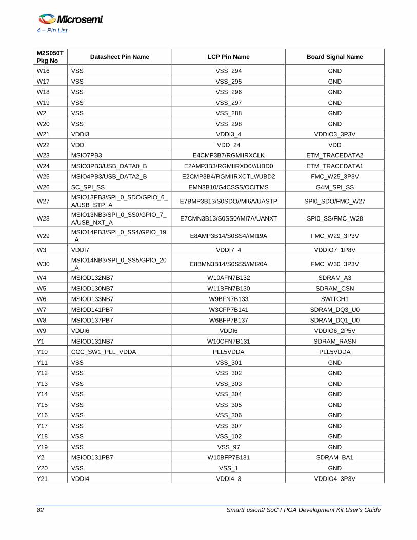
4 – Pin List
82 SmartFusion2 SoC FPGA Development Kit User’s Guide
M2S050T Pkg No Datasheet Pin Name LCP Pin Name Board Signal Name
W16 VSS VSS_294 GND
W17 VSS VSS_295 GND
W18 VSS VSS_296 GND
W19 VSS VSS_297 GND
W2 VSS VSS_288 GND
W20 VSS VSS_298 GND
W21 VDDI3 VDDI3_4 VDDIO3_3P3V
W22 VDD VDD_24 VDD
W23 MSIO7PB3 E4CMP3B7/RGMIIRXCLK ETM_TRACEDATA2
W24 MSIO3PB3/USB_DATA0_B E2AMP3B3/RGMIIRXD0///UBD0 ETM_TRACEDATA1
W25 MSIO4PB3/USB_DATA2_B E2CMP3B4/RGMIIRXCTL///UBD2 FMC_W25_3P3V
W26 SC_SPI_SS EMN3B10/G4CSSS/OCITMS G4M_SPI_SS
W27 MSIO13PB3/SPI_0_SDO/GPIO_6_A/USB_STP_A E7BMP3B13/S0SDO//MI6A/UASTP SPI0_SDO/FMC_W27
W28 MSIO13NB3/SPI_0_SS0/GPIO_7_A/USB_NXT_A E7CMN3B13/S0SS0//MI7A/UANXT SPI0_SS/FMC_W28
W29 MSIO14PB3/SPI_0_SS4/GPIO_19_A E8AMP3B14/S0SS4//MI19A FMC_W29_3P3V
W3 VDDI7 VDDI7_4 VDDIO7_1P8V
W30 MSIO14NB3/SPI_0_SS5/GPIO_20_A E8BMN3B14/S0SS5//MI20A FMC_W30_3P3V
W4 MSIOD132NB7 W10AFN7B132 SDRAM_A3
W5 MSIOD130NB7 W11BFN7B130 SDRAM_CSN
W6 MSIOD133NB7 W9BFN7B133 SWITCH1
W7 MSIOD141PB7 W3CFP7B141 SDRAM_DQ3_U0
W8 MSIOD137PB7 W6BFP7B137 SDRAM_DQ1_U0
W9 VDDI6 VDDI6 VDDIO6_2P5V
Y1 MSIOD131NB7 W10CFN7B131 SDRAM_RASN
Y10 CCC_SW1_PLL_VDDA PLL5VDDA PLL5VDDA
Y11 VSS VSS_301 GND
Y12 VSS VSS_302 GND
Y13 VSS VSS_303 GND
Y14 VSS VSS_304 GND
Y15 VSS VSS_305 GND
Y16 VSS VSS_306 GND
Y17 VSS VSS_307 GND
Y18 VSS VSS_102 GND
Y19 VSS VSS_97 GND
Y2 MSIOD131PB7 W10BFP7B131 SDRAM_BA1
Y20 VSS VSS_1 GND
Y21 VDDI4 VDDI4_3 VDDIO4_3P3V

4 – Pin List
SmartFusion2 SoC FPGA Development Kit User’s Guide 83
M2S050T Pkg No Datasheet Pin Name LCP Pin Name Board Signal Name
Y22 MSIO0PB3 E0AMP3B0/RGMIIMDC ETM_TRACEDATA3
Y23 JTAG_TDI/M3_TDI EMP4/JTAGTDI/CM3TDI G4M_JTAG_TDI
Y24 VPP VPP_4 VPP
Y25 MSIO3NB3/USB_DATA1_B E2BMN3B3/RGMIIRXD1///UBD1 ETM_TRACEDATA0
Y26 VDDI3 VDDI3_5 VDDIO3_3P3V
Y27 VSS VSS_6 GND
Y28 SC_SPI_SDI EMN3B9/G4CSSDI/OCITDI//G4CRXD G4M_SPI_SDI
Y29 SC_SPI_SDO EMP3B10/G4CSSDO/OCITDO//G4CTXD G4M_SPI_SDO
Y3 VDDI7 VDDI7_6 VDDIO7_1P8V
Y30 MSIO12NB3/SPI_0_SDI/GPIO_5_A/USB_DIR_A E7AMN3B12/S0SDI//MI5A/UADIR SPI0_SDI/FMC_Y30
Y4 VSS VSS_299 GND
Y5 VSS VSS_300 GND
Y6 MSIOD142NB7 W3BFN7B142 SDRAM_DQ2_L0
Y7 MSIOD142PB7 W3AFP7B142 SDRAM_DQ0_L0
Y8 CCC_SW1_PLL_VSSA PLL5VSSA PLL5VSSA
Y9 CCC_SW0_PLL_VDDA PLL4VDDA PLL4VDDA


SmartFusion2 SoC FPGA Development Kit User’s Guide 85
5 – Board Components Placement
The SmartFusion2 Development Kit components placement on top and bottom sides, are shown in the following figures.

T1
C54
R97
C48
U10
R55
DS10
R35
J5
D17
R325
U59
T2
C58
C44
C43
C38
C40
R56
DS11
R36
R23
D19
SC1
R74
C42
D7
R52
R24
R25
R339
Q18
Q15
Q14
C200C202
U61
R137
R132
TP29
C37
D5
R26
J4
R338
TP12
J208
J192
J171
J150
SC2
R27
R350
TP24
D16
D14
R244
C119
C121
C120
L10
C74
C70
R28
D6
R353
C198
D15
TP25
C134
L5
C7
C25R33
C26 R37
C18
C172
C104
C103
R680
C100 C9
6
U7
C102
R677
R678
R679
R681
C99
C101
C98C93
R134
R128
J37
R115
C47
C13
J225
U55
R311
R672
R675
R676
C97
R673R674
J117
RS2
R663
J93
U8
C21
C4
C173
U28
J94
U27
J34
C17
C10
J226
U42
TP3
C81
C82
J70
U4
C3
J227
C167
C159
U51
J104
SW9
R148
LED9
C20
R312
U56
C164
C91
R176
R172
J105
J231
J3
Q20
R376
R368
R367
LED1R357
R358
TP22
C162
R286
R283
R282
C146
R265
C92
C86
C85
R175
R173
Q22Q21
R378
R377
R369
LED2 R359
R274
R270
R285
C148
C147
R266
R205
R203
C114
C90
C89
C88
C87
Y2J8
1
TP11
J26
J19
R38
SW4
R13
SW5
Q23
R379
R370
LED4
LED3 R360
R276
R275
R281
R268
C150
C149
J167
R213R215
R212
R217
R207
R206
R204
RS4
RS3
U23
R146
R31
SW3
Q24
R380
R371
LED5R361
R278
R269
R277
R280
C152
C151
RS5 J160
J142
R662
R161
R159
R160
R149
U22
C66
J25
J22
J20
J21
R57
R39
R14
Q26Q25
R381
R372
R373
LED6R362
R363
R267
R279
C153
RS6
L13
J123
C94
C95
R162
J54
R61
R53
R60
R54
SW1
SW2
Q27
R383
R382
R374
LED7 R364
J211
R234R235R236R237
R238
R239
R231R232
R226R229
U40
R183
L8
R184
R182
R179
R177 R178
L7
J33
R89
R88
R87
C50
C49
R72
R79
R75R77
R84
R67
R71
R49
R48
R47
J12
J13
R29
LED8
J185
R240
R241
R242
R256
R218
C128
C129
C131
C130
J124
R185
R180
U36
J82
SW8
C76C7
5C7
3
R145R144R141R139R138
C67
C72C6
9
R135R133
R136
R127R129
C60
C62
C59
R119R122
R126R125
R118R117
R90 R1
07R1
08
R106
R45
C29
C28
J14
TP10
J228
J219
TP14
R247
R220
U45
J151
L12
J125
Y1
R109
R110 R95
C52
R91
R51
R46
U9
R32
J15
J16
J11
TP1
J8J6
Q7
J1
J229
J186
R243
J182
R230J177
R221
R670
J152
J153
SW10
J127J126
Y3
C80
J67
J30
U19
C53
J29
R92R9
3R9
4
R66R68
C32
R30
TP2
Q10
J10
J9
Q8
J220
R219
R150
R111
R112
R100
R85
R76
R64
R62R65
R50
C33
J7
J205
J189
J168J166
J156
J147
J128
J80
R151
R154
R157R1
53R1
52
J32
R113
R80
J17
R355R354TP21
C191
J132
R186R188
R671R181
J116
R167R168
J112
R166
J103
C78
C79
R155
R158
J31
TC5
TC3
TC1
R114 DS
16DS
17DS
18DS
19
R81
R82
R83
DS12
L4
D18
R326
TP13
U37
U33
C77
J49
J44
TC7
TC6
TC2
TC4
DS13
DS14
DS15
CONN
1
D20
R366
R365 C204
U60
R189
DS25
R170
DS22
R131C71
D10
R123SC3
SC4
R102
R103
TP30 Q13
R58
U20
C63
R130
R121
C51
R59
SW6
C6
C694
C693
R375
TP20
J206
J190
J169
J148
R143
D11
C68
C61
U15
R104
R86
C46
R73
R78
R69R70
C39
R21
R22
C205
R356
R346
C189
C186
J207
J191
J170
J149
C111
C105
C84
C135
R347
J221
P1
CR3
CR4
C8 C9
R7
R8Q9
U62
C136
R222
C122
L11
J24
CR2
CR1
U3
R660C683
TP16
R284
J198
U49
J163 C137
C138
C132
R228R224
J164
C126
U43
TP4
C116
J113
J120
R169
J109
J42
R124
J52
C41
J18
R40
J216
U52
C170 R300R2
94R2
93
R298
TP26
U44
R210
R208
R209
TP5
C109
U38
Q17
J85
J71
J36
R96
J2
C196
C199
R343
R348R352
R324C180
U57
C179
C176
R316R313
J204
C169
R301
C168R292
R297
C166
U50
R259
R251
R260
C145
C141
R250
J176
U47
U46
R214C127
R211
C117
U35
R164
R664
J76
J72
J96
J65
J56
J50
J46
U16
C56
L2
R16
C682
R669
R668
C201
R344
R345
R349
R351
C195
J222
R322
R314
C144R264
C165
R255R248
TP27
R223
R225
R216
C123
C124
C118
DS24
DS23
J61J95
DS21
DS20
C57
R98
U11
SW7
C12
U2
Q1R1
DS1
C190
C193
R337
R336
R335
C194
C185
R330
J218
C175
R323
R315
C174
C181J212
C171L15
U53
C161C163
C143
C156
R252
R262
R261
J181
C139
R245
TP28
J157
D13
R201
R199
C112
R197
C115
R200
C110
DS27
U39
R174
R171
J66
J60
J87
J77
J73
J97
J86
R156
J57
J51
J47
R120
U18
R116
R101
TP19
D9D8
R19
R20
R11
D4C2
Q2R2
DS2
C203
R331R328
R327
C177
C178
R321
R287
C154 R257
R271
R253
R263
R254
C157
R246 C140
L14
R202
U41
R195
C108
C106R193
R191
L9
TP8
J99
J98
J88
U24
R105
TP23
R12
Q4Q3
R4R3DS
3
U58
C182
C183
R318
R317
C160 R2
88
U48
C155
C158
R258
R272
R273
R233
C142
R249 R227
J137
R198R196
R194
J100
J101
J89 J90
X1
C64
C65
C55
C22
U6
TP18
R15
D2U1
Q5R5
DS5
DS4
J223
C192
C197R340 R341
R342
C188
R333R332 R3
29
R334
C187
R319
R320
R289
J173
J165
C133
C113
C107
D12
DS26
U34
J102
J84
J91
J78
J74
J62
J68
U21
U17
C45
C11
Q6R6
DS6
J224
R309
R307R308
R306R305
R303R304
R302R299
R291R295R296
J217
R290
J213
J215
J209
J203
J201
J199
J194
J196
J183
J187J193
J178
J174J180
J161
Q19
J158
J154
C125
J145
J143
J140
J138
J136
R190 J1
29
J133
J121
J114
J118
C83
J110
J92
R165
J83
J58R140
R142
R17
R9D3
C1DS
9
DS8
R384
TP7
J130
J234
R192
J75
J64J69
J63
J41
J48
L6J3
9
TP15
Q11
R18
R10
DS7
R187
U32
J79
U26
J53
J35
J27
J23
R34
D1
TP9
J233
J106
R147
R163
U29
J40
RS1
J28
U12
C24 C36
L3
TP17
J230
R385
J214
J210
J200
J202
J197
J188
J195
J184
J179
J172
J175
J162
J159
J155
J146
J144
J141
J139
J232
J135
J134
J122
J131
J115
J119
J111
J55
J45
J43
J38
C27
C15
C184
J108
J107
U30
U25
U13
Q12
R44
C23
C19
C16
C14
L1
U54
U69
J59
U14
C30
R41
R42
C31
R63
C35
C34
U5
R310
U31
R43
65
20
12
17
7
1 6
101
20
12
41
63
17
1
7
6
1
1
71
1
1
11
43
21
1
1
1
ON
ON
21
1 1
1
2
34
1
11
14
3
1
1 2 3
202
7 8 9
12
34
1
3 7 8
1
2
1
2
9
B49
JKLMN
CB
DEFGH
A
1 2 3
9
10
19
20
1
7 8 9
191
1
JKLMN
CDEFGH
BA
1
9
1
5
10
1
10
2
1
1
JKL
MN
CB
DE
FG
H
A
1 2
1
1
31
B11
7
B14B1
3
1
1
1
4
6
7
1
1
1
7
1
8
2
51
15
1
1
2
15
1
51
151
20 19
23 4
1
3
1
REFCLK0_N
ZL RST
1
A123
B
789
R99
M12
11
HPDIFFN4HPDIFFP4
SILKSCREEN (TOP)
REFCLK0_P
C D E F G
M1
GND
SERDES1
GND
TS_MDC
TS_MDIO
H J
1 1
1
P14
P1
A12
A1
DDR3_1P5V
REFCLK0_N
GND
1
1
P2LED2P3LED0
SFP CONN
RXP2
TXP2
RXP0
TXP0
1
11
1
A14
A1
P3LED2
P1LED1
P1LED2
P1LED3
P1LED0
P0LED3
HPOUTCLK5
GND
GND
GND
GND
1P0V_PHY
GND_C
P0LED2
P0LED1
P0LED0
POE PWR ENB
P2LED0P2LED3
P3LED1P3LED3
ON
RXN2
TXN2
RXN0
TXN0
2P5V_LDO
AT FLAG
OFF
RXP3
TXP3
RXN1
TXP1
PGOOD
DVDD12
RXN3
TXN3
RXP1
TXN1
GND_0
GND
1P0V_PHY
POE CONN
13
3
3
3
A1
K1
PCIEXVDD
SERDES0
A1
AK1
50 MHZ
REFCLK0_P
GND
REFP6
REFP5
RevC
3 1
1.2V
1.0V
GND
1 2
3
1
3
3
1
3P3V
3
N23
L23
F30
K25
H28
G29
J29
H30
L26
H26
K23
J27
3
L28
K30
M27
L29
P24
N26
V23
U24
T27
T26
M23
AA29
Y30
V24
3
FMC HEADER
GND
A40
K40
FP4 HEADER
ETM HEADER
GND
PLLMDDRVDDA
A30
JTAG SEL
1
3P3V_LDO
AK30
PLLFDDRVDDA
RVI HEADER
PLLXVDDA
1
FMC HEADER
VPP
DVP-102-000400-001
1
RESET
RST LED
GND
DDR3_VTT
SF2 DEV KIT
USB MICRO AB
USB MINI B
DC JACK12V/6A
HDR-RS485
OTG Support
12V_PCIE
FTDI INTERFACE
12_DCJACK
ANALOG INPUT
DB9-RS232
DB9-CAN2
DB9-CAN1
5P0V
12V
VDDIO
1
3P3V_LDO
OFF
GND
11
ON
12V_POE
1
1
HVDD
HVSS
HVDD
PWR ENBREMOTE
GND
1P8V
1
1
DDR3
-1P5
V
GND
1P8V
3P3V
_LDO
2P5V
_LDO
12P
5V
1
1
HVSS
VDD_
REG
1
V26
1
M25
M24
G30
H27
H291
J30
J28
K24
J26
K29
K28
L30
N24
M26
P23
N25
1
W27
AA28
V22
VDD_REG
2P5V
5P0V
GND
1
1
1
1
R29R24
W28
1
3P3V
12P0
V
13
3
3
3 1
1
5 - Board Components Placement
Figure 27. Silkscreen Top View
86 SmartFusion2 SoC FPGA Development Kit User’s Guide
dogurua
Text Box

R570
C575C520
C495
C472
R547
C394
C399
R536
R527
C348
Y5
R471
R475
R460R467
R610
R611
R605R599
C549
R562
R569
C484
C454
R534
R535
R533
R526
R521
R522
C346
R491
R470
R474
R459R466
R609
R608
R604R598
C529
R560
C420
C419
C337
Y4
R484
R473
R458R465
C239
C583
C565C555
R578
L22
C418
C416
C417
C433
C396
R472
R469
R468R457
R464
R445
C276
R432R435
R437R436
R438
R427
R430
R428R429
R431
R425
R422
R423
R421
R594
C588
C574
C553
C562
C560
R554 C432
R483
R453
R452
R444
R442
R443
R414
R415
R412
R413
C585
C579
C554
C538
R568
C436
C395
R544
R524
C326C331R492
C319C323
C315
C306C312
C294C301
C289
R476
R479
R451
R450
R449
C278
C279
R418
R416
R417
R419
R420
C236
C582
C566
R567
R542 R543
R523
C336C338
C328
C327
C329
C314C318
C324
C311C305
C322
C297
C298
C299
C296 C292 C287R478
C351
R454
R447
R446
R448
R424
C233
R545
C382
C325C330
C321C317
C304C310R4
85C308
C293C300
C288
C291
R497
R499
R498
C277
L18
C263
C250
C216
C211
R551
R553
R546
R548
C385
C384
C377
L21
C376
C364
C359
R496
R504
R495
C225C222
C217L17
C206
R400
R403
R401
R402
C678
R494
C268
C257
C260
C244
C243
C245
R426
C221L16
C213 C212
R398
R399
C681
C347
C340
C286C285
C290C295
C267C262
C252
C259
C256
C242
C247
D20
C380
C369
C264C266
C261R433
C253C255
C251
C258
C246
R657
R539
R537
C366
D19
SC5
Q30
R507
D21
C690 C691
C692
D22
C379
C358
C362
R489
R456
R434
C689
C679
R532
Q29
Q28
C254
R656
R587
U67
C386
C378
C381
R502R508R510
R500
C309
D15
D14
R596
D23
R595
R580
C353
C687
C688
C598
C587
C580
C219
R618
R581
C207
R395
C680
C609
R582
R573
C220
C218
C210R4
05R397
R396
R658
C608
C606
R588
C528
R575
R501
R493
R408
C209
R404
R620
C619
C605
C599
C596
C584
C571
R586
R585
C559
R572
R571
C409
C388
R520
C373
R666R667
U68
C602
R661
C570
R574
R576
C391
R525
C375
R518
R516
C284
R477
C282
C224
C208
C684
R665
C669
C586
C387
C374
C283
R480
R461
R455
R441
R394
C628
C620
C612
R558
C390
C352
C342
C302
D8
C215
R393
C642
C611
C604
R561
C455
R519
C361
L20 C3
44C334
C333
R391
R392
C677
L23
R635
R636
C641
R619
C597
C356
C350
C360
L19
C343
C349
R490
C339 C332
D2R390
R659
R623
C491
R517
R487
R488
C281
C234
C223
R389
C428
C407
C320
C280
C272
C265
C214
R386
R387
C335
C316
C313
D1
R388
R506
C345
R440
C365
C363
R439
C271
C235
C226
R512
R511
R514
R513
C341
R486
R482
R463
C275
C270
R407
C230C232
C228
C645
C653
C665
C637
C627
C542
C506
Y6C237
R406
R627
C631
C640
C618
C486
C438
C367
C685
R481
R462
C269
C274
R411
R410
C238
C664
C656
C626
C648C634
C617
C595
RS10
C593
RS9
RS8
RS7
C303
C273
R409
C241
C227
C229
C652
C663
C636
C625
C525
C471
C482
C357
C307
C249
C644R626
C639C630
C616
R579
C573
C485
C446
U66
R515
C368
R509
C240
C248
U64
C662
C655
C633
C647
R624
C624
C615
RS11
C592
C661
R638R633
R642
C623
C635
R631R628
C614
C603
R593
C591
R541
C372
U70
C561
C578C569
C558C552C548
C505C523
C490
C475
C453
C481
R559
C422C412
R557
C403
U65
C672
C671
R655
R654R648
R653
C670
R646
R634R639R641R644
C643
C638
C651
R597
R616
R591
R592
C393
C383
C371
C355
R503R505 C6
86
C572 C564
C524 C5
19C544
C503
C504
C527
C541C533
C489
C498C4
92C465 C4
50
C474C480C479
C470
C449C448
C435
C414
C415
C445
R552R555
C402C401
C406
U63
R650
R652
R651
C673
C674
C675
C660
R629
R625
C629C613
R621
R617
C601
C590
R540
C392
R531
C354
C547
C551
C563
C568
C557
C577
C526
C514
C518
C517
C516
C515
C540C532C5
31C530
C500C494C488
C468C462
C463
C464
C476
C461
C443
C444
C442
C431
C434C426
C427
C411 C408
C441
C405
C398
C400
C231
C676
C654
C622
C646
C632
C621
R622
C600
R590
C589
R530
R528
R529
C546
C576
C545C556
C567
R577
C512
C513
C511
C535
C536
C537
C510
C459
C460
C458
C430C421
C440C425
C423
C439
C410
C424
C437C447 R5
56R550C404
C397
R649
C668
R640R637
R645R647
C650
R643
R630R632C649
C610
R602C607
R601
R589
C594
C389
R538
C581R583C550
C508
C534
C501
C509
C522 C507C5
02
C539
C499
C487C493
R563R564
C451
C456
C473C469
C478
C457C452
C467
C413
C429
R549
C667
C657C658C659C666
R615
R614R6
07
R603
C370
C543
C521
C496
C497
C483
R565
R566
C477
C466
R613
R612
R600R606
R584
6
3
4
3
64
79 8
N
L
J
M
K
C
G
E
B
H
D
A
2 13 378
A49
9
M
K
N
L
JH
F
DC
G
E
BA
2 1379 8
A1A11A14
N
L
J
M
K
C
G
E
H
F
D
A
2 1
B
P1P14
A30
AAK30
305-PD-12-1067
A1A14
A
AK1
A1
100 MHZ100 MHZ
SILKSCREEN (BOTTOM)
C
C
BB
Testing the Hardware
Figure 28. Silkscreen Bottom View
SmartFusion2 SoC FPGA Development Kit User’s Guide 87
dogurua
Text Box
dogurua
Text Box


SmartFusion2 SoC FPGA Development Kit User’s Guide 89
6 – Demo Design
SF2-DEV-KIT-PP Board Demo Design The SmartFusion2 SF2-DEV-KIT-PP comes with a preloaded demo design. This demo design demonstrates key SmartFusion2 device features such as - PCIe, USB, DDR3, SPI flash, I2C, Flash*Freeze, GPIOs and Fabric interface controller of the SmartFusion2 device. These features can be used for rapid prototyping and validation of user specific designs. Note: For more details about the running the demo design, refer to the SmartFusion2 SoC FPGA: Development Kit
Demo User’s Guide.
Figure 29. Test Menu for Demo Design


SmartFusion2 SoC FPGA Development Kit User’s Guide 91
7 – Manufacturing Test
SF2-DEV-KIT-PP Board Testing Procedures SmartFusion2 SF2-DEV-KIT-PP contains a manufacturing test program that can be run to verify the functionality of the board. This program contains a list of options that can be run as diagnostics. After setting up HyperTerminal and the board is powered up the menu options are displayed, as shown in Figure 27. From the list of provided menu options, either one or all of the tests can be selected to verify the functionality. Note: For more details about the manufacturing test procedures, associated files, and updated information refer to
http://www.microsemi.com/soc/download/rsc/?f=%20SF2-DEV-KIT-PP_Mfg_PF (to be released).
Figure 30. HyperTerminal Test Menu

SmartFusion2 SoC FPGA Development Kit User’s Guide 93
List of Changes
Revision Changes Page
Revision 2 (March 2013)
Added 6 – Demo Design section. 89
Revision 1 (March 2013)
SmartFusion2 device package name is modified from FG896 to FGG896 (SAR 45584). NA
The Current Measurement section is added (SAR 45584). 25
Updated Hardware Installation section (SAR 45584). 11
Note: The revision number is located in the part number after the hyphen. The part number is displayed at the bottom of the last page of the document. The digits following the slash indicate the month and year of publication.


SmartFusion2 SoC FPGA Development Kit User’s Guide 95
Product Support
Microsemi SoC Products Group backs its products with various support services, including Customer Service, Customer Technical Support Center, a website, electronic mail, and worldwide sales offices. This appendix contains information about contacting Microsemi SoC Products Group and using these support services.
Customer Service Contact Customer Service for non-technical product support, such as product pricing, product upgrades, update information, order status, and authorization.
From North America, call 800.262.1060 From the rest of the world, call 650.318.4460 Fax, from anywhere in the world 408.643.6913
Customer Technical Support Center Microsemi SoC Products Group staffs its Customer Technical Support Center with highly skilled engineers who can help answer your hardware, software, and design questions about Microsemi SoC Products. The Customer Technical Support Center spends a great deal of time creating application notes, answers to common design cycle questions, documentation of known issues and various FAQs. So, before you contact us, please visit our online resources. It is very likely we have already answered your questions.
Technical Support Visit the Microsemi SoC Products Group Customer Support website for more information and support (http://www.microsemi.com/soc/support/search/default.aspx). Many answers available on the searchable web resource include diagrams, illustrations, and links to other resources on website.
Website You can browse a variety of technical and non-technical information on the Microsemi SoC Products Group home page, at http://www.microsemi.com/soc/.
Contacting the Customer Technical Support Center Highly skilled engineers staff the Technical Support Center. The Technical Support Center can be contacted by email or through the Microsemi SoC Products Group website.
Email You can communicate your technical questions to our email address and receive answers back by email, fax, or phone. Also, if you have design problems, you can email your design files to receive assistance. We constantly monitor the email account throughout the day. When sending your request to us, please be sure to include your full name, company name, and your contact information for efficient processing of your request. The technical support email address is [email protected].
My Cases Microsemi SoC Products Group customers may submit and track technical cases online by going to My Cases.

Product Support
96 SmartFusion2 SoC FPGA Development Kit User’s Guide
Outside the U.S. Customers needing assistance outside the US time zones can either contact technical support via email ([email protected]) or contact a local sales office. Sales office listings can be found at www.microsemi.com/soc/company/contact/default.aspx.
ITAR Technical Support For technical support on RH and RT FPGAs that are regulated by International Traffic in Arms Regulations (ITAR), contact us via [email protected]. Alternatively, within My Cases, select Yes in the ITAR drop-down list. For a complete list of ITAR-regulated Microsemi FPGAs, visit the ITAR web page.


50200394-1/03.13
Microsemi Corporate Headquarters One Enterprise, Aliso Viejo CA 92656 USA Within the USA: +1 (949) 380-6100 Sales: +1 (949) 380-6136 Fax: +1 (949) 215-4996
Microsemi Corporation (NASDAQ: MSCC) offers a comprehensive portfolio of semiconductor solutions for: aerospace, defense and security; enterprise and communications; and industrial and alternative energy markets. Products include high-performance, high-reliability analog and RF devices, mixed signal and RF integrated circuits, customizable SoCs, FPGAs, and complete subsystems. Microsemi is headquartered in Aliso Viejo, Calif. Learn more at www.microsemi.com.
© 2013 Microsemi Corporation. All rights reserved. Microsemi and the Microsemi logo are trademarks of Microsemi Corporation. All other trademarks and service marks are the property of their respective owners.