—Recent Progress in Si-LSIs to Extend...
10
36 SCIENCE & TECHNOLOGY TRENDS 3 Applying Nanotechnology to Electronics —Recent Progress in Si-LSIs to Extend Nano-Scale — HIROSHI KOMATSU (Information and Communications Research Unit) * ATSUSHI OGASAWARA (Affiliated fellow) ** ** * ** Atsushi Ogasawara Chief Scientist, National Institute of Advanced Industrial Science and Technology (AIST) http://www.aist.go.jp/ 1 Introduction Nanotechnology broadly includes all technologies that handle nano-scale materials, and in a narrow sense, technologies that handle unique phenomena that arise in the 10-to-100-nm size range. Materials of these sizes have been prepared using two techniques, the top-down and the bottom-up methods [1] . The top-down method is applied to process macro-scale materials into smaller sizes just as in the semiconductor process, whereas the bottom-up method is applied to integrate molecules or atoms into nano-scale materials just as a living organism synthesizes DNA and proteins, and integrates them into a cell, and further, into a body (Figure 1). The design rule of commercially available LSIs has already reached 90 nm [2] . The top-down method plays a major role in research in the U.S. and other foreign countries. Research programs are planned to expand the industrial life span of the Si-LSI technology [3] . Following the “21st Century Nanotechnology Research and Development Act” in the U.S. [4, 5] , which plans to assess the application possibility of self-assembly as soon as possible, the bottom-up method has been successfully combined using the top-down method by researchers in U.S. universities and companies, showing that nanotechnology is being smoothly extended to conventional electronics. The bottom-up method is epitomized by self-assembly, which plays an important role in nanotechnology, together with prospective applications in ionics and electronics. In addition to the primitive assembly of materials, nanotechnology is moving forward to electronic devices and their integration. This paper discusses recent progress and current trends in nanotechnology R&D towards industrial application, referring to publications at conferences and journals relating to Si-LSI technology. 2 Architecture Levels of the Si-LSI Technology One candidate in constructing an electronic device using the bottom-up method is to combine it with the top-down method. When the device is constructed using not only the bottom-up method, we must examine the following: Figure 1 : Two methods to approach to nano-scale
Transcript of —Recent Progress in Si-LSIs to Extend...

36
S C I E N C E & T E C H N O L O G Y T R E N D S
37
Q U A R T E R L Y R E V I E W N o . 1 6 / J u l y 2 0 0 5
3
Applying Nanotechnology to Electronics—Recent Progress in Si-LSIs to Extend Nano-Scale —
HIROSHI KOMATSU (Information and Communications Research Unit)*
ATSUSHI OGASAWARA (Affiliated fellow)**
***
** Atsushi Ogasawara Chief Scientist, National Institute of Advanced Industrial Science and Technology (AIST) http://www.aist.go.jp/
1 Introduction
Na not e ch no lo g y b r o a d l y i nc lu d e s a l l
technologies that handle nano -scale materials,
and in a narrow sense, technologies that handle
unique phenomena that arise in the 10-to-100-nm
size range.
Materials of these sizes have been prepared
using two techniques, the top -down and the
bottom-up methods[1]. The top -down method
is applied to process macro-scale materials into
smaller sizes just as in the semiconductor process,
whereas the bottom-up method is applied to
integrate molecules or atoms into nano - scale
materials just as a living organism synthesizes
DNA and proteins, and integrates them into a cell,
and further, into a body (Figure 1). The design
rule of commercially available LSIs has already
reached 90 nm[2].
The top -down method plays a major role in
research in the U.S. and other foreign countries.
Research programs are planned to expand the
industrial life span of the Si-LSI technology[3].
Following the “21st Century Nanotechnology
Research and Development Act” in the U.S.[4, 5],
which plans to assess the application possibility
of sel f - a ssembly as soon as possible, the
bot tom - up method has been successfu l ly
combined using the top - down method by
researchers in U.S. universities and companies,
s how i ng t h a t n a no t e ch no lo g y i s b e i ng
smoothly extended to conventional electronics.
The bot tom - up method i s epitomized by
self - assembly, which plays an important role
in nanotechnology, together with prospective
appl ications in ionics and electronics. In
addition to the primitive assembly of materials,
nanotechnology is moving forward to electronic
devices and their integration.
This paper discusses recent progress and
current trends in nanotechnology R&D towards
industrial application, referring to publications
at conferences and journals relating to Si -LSI
technology.
2 Architecture Levels of the Si-LSI TechnologyOne candidate in constructing an electronic
device using the bottom-up method is to combine
it with the top-down method. When the device
is constructed using not only the bottom-up
method, we must examine the fol lowing:
Figure 1 : Two methods to approach to nano-scale
36
S C I E N C E & T E C H N O L O G Y T R E N D S
37
Q U A R T E R L Y R E V I E W N o . 1 6 / J u l y 2 0 0 5
the architecture of the conventional Si - LSI
technology, the interface between the bottom-up
method and the Si-LSI technology, and the extent
of the influence of the bottom-up method on
Si-LSI technology.
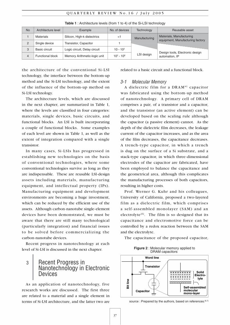
The architecture levels, which are discussed
in the next chapter, are summarized in Table 1,
where the levels are classified in four categories:
materials, single devices, basic circuits, and
functional blocks. An LSI is built incorporating
a couple of functional blocks. Some examples
of each level are shown in Table 1, as well as the
extent of integration compared with a single
transistor.
In many cases, Si - LSIs has progressed in
establishing new technologies on the basis
of conventional technologies, where some
conventional technologies survive as long as they
are indispensable. These are reusable LSI-design
assets including mater ia ls, manufactur ing
equipment, and intel lectual property (IPs).
Manufacturing equipment and development
environments are becoming a huge investment,
which can be reduced by the efficient use of the
assets. Although carbon-nanotube single-element
devices have been demonstrated, we must be
aware that there are still many technological
(particularly integration) and financial issues
to be solved before commercia l i z ing the
carbon-nanotube devices.
Recent progress in nanotechnology at each
level of Si-LSI is discussed in the next chapter.
3 Recent Progress in Nanotechnology in Electronic DevicesAs an application of nanotechnology, f ive
research works are discussed. The first three
are related to a material and a single element in
terms of Si-LSI architecture, and the latter two are
related to a basic circuit and a functional block.
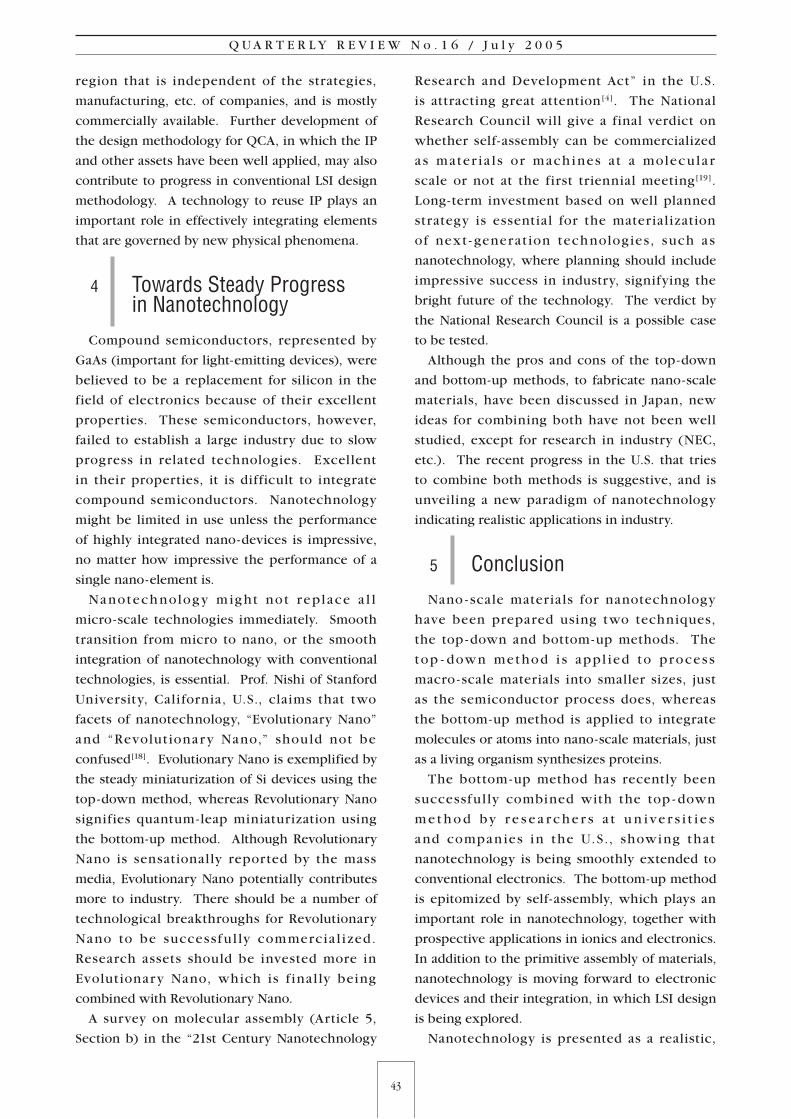
3-1 Molecular Memory A dielectr ic f i lm for a DR AM*1 capacitor
was fabricated using the bottom-up method
of nanotechnology. A primary cell of DRAM
comprises a pair, of a transistor and a capacitor,
and the transistor (an active element) can be
developed based on the scaling rule although
the capacitor (a passive element) cannot. As the
depth of the dielectric film decreases, the leakage
current of the capacitor increases, and as the area
of the film decreases, the capacitance decreases.
A trench - type capacitor, in which a trench
is dug on the surface of a Si substrate, and a
stack-type capacitor, in which three-dimensional
electrodes of the capacitor are fabricated, have
been employed to balance the capacitance and
the geometrical area, although this complicates
the manufacturing processes of both capacitors,
resulting in higher costs.
Prof. Werner G. Kuhr and his colleagues,
University of California, proposed a two-layered
f i lm as a dielectr ic f i lm, which comprises
a sel f - assembled monolayer (SAM) and an
electrolyte[6]. The film is so designed that its
capacitance and electromotive force can be
controlled by a redox reaction between the SAM
and the electrolyte.
The capacitance of the proposed capacitor,
Table 1 : Architecture levels (from 1 to 4) of the Si-LSI technology
No Architecture level Example No. of devices Technology Reusable asset
1 Materials Silicon, High-k dielectrics <1 ManufacturingMaterials, Manufacturing equipment, Manufacturing factory
2 Single device Transistor, Capacitor 1
3 Basic circuit Logic circuit, Delay circuit 10 - 102
LSI design Design tools, Electronic design automation, IP 4 Functional block Memory Arithmetic-logic unit 102 - 108
Figure 2 : Molecular memory applied to DRAM capacitors
source : Prepared by the authors, based on references.[6,7]

38
S C I E N C E & T E C H N O L O G Y T R E N D S
39
Q U A R T E R L Y R E V I E W N o . 1 6 / J u l y 2 0 0 5
which is in contrast to the conventional capacitor
fabricated by insulation films such as silicon
oxide, is governed by the molecule number
in the SAM (or an area of the capacitor) and
is independent of applied voltage, showing
that the capacitance is more than 10 times the
conventional capacitance. The charge retention
time of the proposed capacitor is governed by
the properties of the molecule, and is more
than 10,000 times (more than 10s) that of the
conventional capacitor, in which the retention
time is governed by charge leakage at the silicon
oxide film.
The molecule accommodates multiple states
and potentials, which leads to a multiple-value
memory and a multiple-value logic gate*2. The
SAM is fabricated on a silicon or metal substrate
allowing the self-alignment of molecules, and
is compatible with the present semiconductor
manufacturing equipment. ZettaCore*3 [7],
a venture company in the U.S., applied this
technology to fabricating a 1 Mbit DRAM, whose
electronic characteristics were assessed showing
a promising future.
3-2 Fine ProcessingF l a sh memor y *4, a m a jo r non - vo l a t i l e
semiconductor memory, comprises a unit of
a single transistor, in contrast to DRAM that
comprises a unit of two elements (one transistor
and one capacitor). The flash memory is rapidly
expanding its market into commercial products,
such as price - sensitive consumer electronics
products, owing to its advantages of high
integration and low price. Highly integrated flash
memory is in big demand for portable devices,
such as cellular phones, and can now show static
and dynamic images that require larger memory
capacity[8].
Flash memory has a size limit in the depth
of the tunneling oxidized film (Figure 3A). A
floating-gate -type transistor, a typical element
of f lash memory, stores information using a
charge at the floating gate that is fabricated by
stacking two gates. A charge is injected through
the tunneling oxidized film by applying voltage
at the control gate. The tunneling oxidized gate
(generally SiO2) must be sufficiently insulating
to store the charge during the guaranteed data
retention period (generally 10 years). The depth
of the tunneling oxidized film cannot therefore
be reduced in accordance with the scaling rule,
and is limited to beyond a certain depth. This
prevents transistors in f lash memory from
being miniaturized further and prevents the
operating voltage from being reduced, which is
essential for reducing power consumption and
for sharing a common power supply with other
low-operating-voltage components.
A new structure that may solve the problem has
been presented, where the floating gate is replaced
by a number of nano-dots (non-continuous film)
(Figure 3B). A charge-accumulating electrode
made of continuous film does not work when the
film contains at least one defect, while an electrode
made of a non-continuous film works sufficiently
even when the film contains a certain amount of
defects, although a few fractions of the charge
Figure 3 : Schematic cross-sections of a flash-memory basic device

38
S C I E N C E & T E C H N O L O G Y T R E N D S
39
Q U A R T E R L Y R E V I E W N o . 1 6 / J u l y 2 0 0 5
are lost (Figure 3C). The nano -dot tunneling
oxidized film provides higher fault tolerance and
allows thinner depth of the film[9].
When nano - dots are fabricated using the
conventional semiconductor process, the size
and geometr ical placement of dots are not
well controlled as designed, which leads to
non-reproducible devices[10]. This suggests that
a new technique is needed to fabricate nano-dots
of a designed, uniform size.
Researchers at IBM in the U.S., presented a new
technique using self-assembly to fabricate silicon
nano-dots at the International Electron Devices
Meeting in 2003[11].
The researchers developed a new technique
to fabricate nano -dots using the self-assembly
of organic polymer materials, without using
conventional l ithography. This technique
provides nano -dots with smaller size, higher
density, better geometrical precision, and better
uniformity than conventional lithography. The
high-resolution SEM photograph indicates that
silicon nano -dots are fabricated between the
control gate (polysil icon) and the substrate
(silicon) of a uniform size of about 20 nm (Figure
4).
The researchers in IBM successfully report
that a charge - accumulating electrode can be
fabricated combining the top - down method
(conventional lithography) with the bottom-up
method (sel f - assembly), which solves the
problems of the conventional method.
Figure 4 : Fabrication flow of silicon nano-dots
Source: Reference [11]. The schematics were prepared by the authors.
A: schematic cross-sections of each process, B: top-views of A, C: cross-section of the fabricated transistor. In the figure B-d, a: diameter of the self-assembled polymer (broken line), b: diameter of the silicon nano-dots in the middle of formation, c: diameter of the formed silicon nano-dots. A- a (the first stage): Phase separation in a micro size occurs when the diblock copolymer is heated, where the diblock copolymer is
comprised of two polymer blocks hardly soluble each other (polystyrene/poly(methylmethacrylate) (PMMA) = 70/30) . After the phase separation takes place at 180˚C, the PMMA domain is selectively removed by solving in an acetic acid. The honeycomb-like polystyrene formed by self-assembly is left. The size of the honeycomb is governed by molecular size of the diblock copolymer. The black part of B-a, -b, and -c is about 20 nm in diameter and about 40 nm in separation.
A- b (the second stage): A silicon oxidized film is processed in nano-scale using the self-assembled polymer as a mask, which is removed afterwards.
A- c (the third stage): the holes formed by the second stage are filled with silicon applying the conventional semiconductor process. Finally, silicon nano-dots are formed using the self-assembled polymer as a template.

40
S C I E N C E & T E C H N O L O G Y T R E N D S
41
Q U A R T E R L Y R E V I E W N o . 1 6 / J u l y 2 0 0 5
3-3 Electro-Migration Switch Using IonsSome LSIs are used after changing the wiring
among their elements inside, giving priority
to either processing speed or low power
consumption. The rewiring has conventionally
been conducted by thermal cutting using a high
electric current or irradiating with a laser beam.
Conventional rewiring is non-reversible and may
damage neighboring elements, which grows
more serious as the patterning becomes finer. As
an alternative, transistors are used as reversible
switches, although this technique is accompanied
by response delay, larger size, and higher power
consumption.
Researchers in IBM, U.S.A., presented a new
technique using electro -migration (IBM calls
it “eFuse”) in July, 2004, where circuits are
autonomically reconstructed[12].
Electro -migration is the migration of metal
atoms in solids when electric current flows at
high density, which has been avoided due to the
malfunction of LSIs.
The eFuse of IBM uses electro -migration for
rewiring elements, cells, and units inside LSIs.
The eFuse features reproducible fine wiring
(about 100 nm) without damage (Figure 5).
Together with prioritizing both processing
speed and low power consumption, the eFuse
is designed to repair itself; where a failure is
detected, the failure cell or unit is isolated and
replaced by another cell or unit. Furthermore, it
is designed to avoid failures by wiring resistance
being adjusted depending on the load.
IBM is trying to establish an “autonomic”
computer that controls and repai rs itsel f.
The eFuse, which is a technology based on
hardware, contrasts with autonomic computing,
which is based on software. IBM considers
the so - far -problematic electro -migration as a
next-generation technology related to reversible
switches or as a technological seed to renovate
computer hardware.
N EC Cor por at ion ( N EC ) , the Nat iona l
Institute for Materials Science (NIMS), and
the Japan Science and Technology Agency
( JST), in Japan, are jointly developing a small,
low-resistance switch using dendrite formation in
a solid electrolyte. This switch is based on atomic
switching in which electrodes are reversibly
connected by the electrochemical formation of
metal dendrites[13].
A programmable logic circuit, which allows
f lexible and timely development, is attracting
Figure 5 : Photographs of eFuse (left: top view, right: cross-section)
Atom migration occurred at the part where color is changed. Source: Reference [12]
Figure 6 : Electro-migration switch using metal ions in a solid electrolyte
When a minus voltage is applied to the Ti electrode, Cu is oxidized to Cu+ on its electrode, which dissolves into Cu2S. Cu+ is reduced to Cu on the Ti electrode, which deposits on the electrode as metal Cu. When the deposited Cu forms dendrite to bridge two electrodes, the switch turns on. When a plus voltage is applied to the Ti electrode, the opposite reactions take place to turn the switch off.
Source: Reference [14]

40
S C I E N C E & T E C H N O L O G Y T R E N D S
41
Q U A R T E R L Y R E V I E W N o . 1 6 / J u l y 2 0 0 5
the attention of electronic- device engineers.
The conventional programmable circuit has
disadvantages, however, and is relatively slow in
processing speed and high in power consumption
due to the larger size of the programmable
switches. The recent progress, as shown above,
has the fol lowing implications: fabrication
without lithography, smaller size (about 1/30 in
area), lower wiring resistance (about 1/10), and
shorter signal delay (shortened by 20 to 40%).
The atomic switch provides a reversible
on/off as well as the eFuse of IBM. Further, the
switch has the potential to provide the dynamic
programming of logic circuits, in which circuits
are re-programmed during operation, as well as
static programming, in which circuits are built as
designed.
3-4 Device ArraysIt is being attempted to combine conventional
integrated circuits, which are even now being
miniaturized further using the top-down method,
with nano-tubes or nano-wires, which focuses on
the elements that need to be further reduced in
size[15,16].
Designed in the architecture above, the LSI
accommodates pattern-size Fs (repetitive -size:
Fs) in pattern-size F (repetitive size: 2 x F, F >
Fs), where the pattern-size F is achieved using
conventional lithography, and the pattern-size Fs
is achieved without lithography (Figure 7). The
periodic pattern fabricated by the pattern-size Fs
is ready to construct functional blocks, such as a
memory cell or gate arrays, in which transistors
are periodically arranged.
A primary device in the cell is a logic circuit
built by diodes or transistors that are built by
crossing nano-wires.
In this LSI design, the connection between
circuits constructed by conventional lithography
and arrays of nano -wires, etc. is realized as a
key technology. A decoder built using the 2 x Fs
repetitive size is proposed for binding the 2 x F
and the 2 x Fs, whereas the decoder must be built
without using lithography. Doping to nano-wires
or nano-imprinting*5 may be a solution.
Although this design must be accompanied
by technological breakthrough in bui lding
the decoder, the research is of significance
in clar i f ying current design obstacles. I f
Figure 7 : Circuit architecture based on arrays, such as nano-wires
Source: Prepared by the authors, based on references [15, 16]

42
S C I E N C E & T E C H N O L O G Y T R E N D S
43
Q U A R T E R L Y R E V I E W N o . 1 6 / J u l y 2 0 0 5
the problems are solved using the present
manufacturing technology, the LSI design has the
potential for immediate commercialization.
3-5 QCA* 6 Logic LSIThe present LSI is designed from an upper
arch itecture (h igh ly abstract) to a lower
( lowly abstract), where each design step is
precisely described. This f low has worked
effectively in the design of a large - scale LSIs
with some restr ictions. Design errors are
detected by modeling and verifying at each
step, by which effective design is achieved for
still -now-expanding LSIs without re -modeling.
T h e d e s c r i b e d m o d e l i s d e p e n d e n t o n
manufacturing technology because this f low
becomes less abstract, or more realistic, from
the upper to the lower. The present LSIs based
on CMOS are likely, at levels lower than the
logic circuit in Figure 8, to be modified due to
the conditions and limitations of manufacturing
technologies.
A design methodology is under development
to ef fect ively des ign a h igh ly integrated
system based on QCA[17], whereby the design
methodology for LSIs is more or less modified.
QCA is attractive because the element of QCA
is potentially reduced in size to less than that of
CMOS. Although the architecture of QCA was
proposed more than ten years ago, its impressive
application to integrated circuits has not yet been
reported. The lack of a design methodology for
QCA by which functional elements are integrated
into a system accounts for some of difficulties
facing QCA.
Prof. Steven C. Henderson and colleagues
of Valparaiso University, Indiana, U.S.A., have
developed a design methodology that builds
a structured model of elements and conducts
model i ng a nd ver i f icat ion on the lower
architecture [17]. For example, a hardware
description language*7 has been developed,
which is a design tool for construct ing a
structured model of elements from a logic model.
In addition, an integrated design methodology
for QCA has been proposed, whereby the layout
for each QCA cell in the lower architecture is
constructed, and its performance is simulated.
Complicated LSIs have recently been effectively
designed in a short period using commercially
available, reusable LSI design assets (IP). The
IP is placed in a technological intermediate
Figure 8 : LSI design flow and modifications for being integrated with manufacturing
Source: Prepared by the authors, based on reference [17]
42
S C I E N C E & T E C H N O L O G Y T R E N D S
43
Q U A R T E R L Y R E V I E W N o . 1 6 / J u l y 2 0 0 5
region that is independent of the strategies,
manufacturing, etc. of companies, and is mostly
commercially available. Further development of
the design methodology for QCA, in which the IP
and other assets have been well applied, may also
contribute to progress in conventional LSI design
methodology. A technology to reuse IP plays an
important role in effectively integrating elements
that are governed by new physical phenomena.
4 Towards Steady Progress in NanotechnologyCompound semiconductors, represented by
GaAs (important for light-emitting devices), were
believed to be a replacement for silicon in the
field of electronics because of their excellent
properties. These semiconductors, however,
failed to establish a large industry due to slow
progress in related technologies. Excellent
in their properties, it is difficult to integrate
compound semiconductors. Nanotechnology
might be limited in use unless the performance
of highly integrated nano-devices is impressive,
no matter how impressive the performance of a
single nano-element is.
Nanotech nolog y m ig ht not replace a l l
micro-scale technologies immediately. Smooth
transition from micro to nano, or the smooth
integration of nanotechnology with conventional
technologies, is essential. Prof. Nishi of Stanford
University, Cali fornia, U.S., claims that two
facets of nanotechnology, “Evolutionary Nano”
and “Revolut ionar y Nano,” shou ld not be
confused[18]. Evolutionary Nano is exemplified by
the steady miniaturization of Si devices using the
top-down method, whereas Revolutionary Nano
signifies quantum- leap miniaturization using
the bottom-up method. Although Revolutionary
Nano is sensationally reported by the mass
media, Evolutionary Nano potentially contributes
more to industry. There should be a number of
technological breakthroughs for Revolutionary
Nano to be successfu l ly commercia l i zed.
Research assets should be invested more in
Evolutionary Nano, which is f inal ly being
combined with Revolutionary Nano.
A survey on molecular assembly (Article 5,
Section b) in the “21st Century Nanotechnology
Research and Development Act” in the U.S.
is attracting great attention[4]. The National
Research Council will give a final verdict on
whether self-assembly can be commercialized
a s mater i a l s or mach i nes at a molecu la r
scale or not at the first triennial meeting[19].
Long- term investment based on well planned
strategy is essential for the material ization
of next - generat ion technolog ies, such as
nanotechnology, where planning should include
impressive success in industry, signifying the
bright future of the technology. The verdict by
the National Research Council is a possible case
to be tested.
Although the pros and cons of the top-down
and bottom-up methods, to fabricate nano-scale
materials, have been discussed in Japan, new
ideas for combining both have not been well
studied, except for research in industry (NEC,
etc.). The recent progress in the U.S. that tries
to combine both methods is suggestive, and is
unveiling a new paradigm of nanotechnology
indicating realistic applications in industry.
5 ConclusionNano - scale materials for nanotechnology
have been prepared using two techniques,
the top - down and bottom-up methods. The
top - down method i s appl ied to process
macro - scale materials into smaller sizes, just
as the semiconductor process does, whereas
the bottom-up method is applied to integrate
molecules or atoms into nano-scale materials, just
as a living organism synthesizes proteins.
The bottom-up method has recently been
successful ly combined with the top - down
m e t h o d by r e s e a r c h e r s a t u n i ve r s i t i e s
and compan ies in the U.S., showing that
nanotechnology is being smoothly extended to
conventional electronics. The bottom-up method
is epitomized by self-assembly, which plays an
important role in nanotechnology, together with
prospective applications in ionics and electronics.
In addition to the primitive assembly of materials,
nanotechnology is moving forward to electronic
devices and their integration, in which LSI design
is being explored.
Nanotechnology is presented as a realistic,

44
S C I E N C E & T E C H N O L O G Y T R E N D S
45
Q U A R T E R L Y R E V I E W N o . 1 6 / J u l y 2 0 0 5
promising technology for the future due to recent
progress in this field, where nanotechnology is
combined with conventional Si-based electronics.
L o ng - t e r m i nve s t me nt b a s e d o n we l l
planned strategy is essential for materializing
n e x t - ge n e r a t i o n t e c h n o l o g i e s , s u c h a s
nanotechnology, where planning should include
impressive success in industry, signifying the
bright future of the technology.
Although the pros and cons of the top-down
and bottom-up methods have been discussed in
Japan, new ideas for combining both have not
been well studied, except for research in industry
(NEC, etc.). The recent progress in the U.S. that
tries to combine both methods is suggestive, and
is unveiling a new paradigm of nanotechnology
indicating realistic applications in industry.
Acknowledgments
The authors thank Prof. Yoshio Nishi of
Stanford University for his valuable comments.
Glossary
*1 DRAM A semiconductor memory device that allows
random access (read and write). Mainly
used for the main memory of a computer.
*2 Status has discrete values A molecule containing a multi -porphyrin
nano-structure has, reportedly, a maximum
of e ight mu lt iple ox idat ion s t ates [4 ].
Porphyrin is an organic pigment.
*3 ZettaCore A venture company established in 1999 by
researchers of University of California and
North Carolina State University.
*4 Flash memory Electrically rewritable non-volatile memory,
where all or a block of data can be erased.
*5 Nano-imprint Appl icat ion of meta l press i ng us i ng
molds to nanotechnology. A nano - scale
printing technology in which a mold with
micro-patterns is impressed onto a material
such as a plastic film.
*6 QCA Cellular automata (CA) are, by definition,
dynamical f inite - state machines. On a
regular lattice (repeated structure of points
has the same kind of neighborhood), one
places a finite-state machine at each point.
The machine changes its state as a function
of states of its neighbors and its own state.
The states of all machines in the lattice are
updated synchronously and simultaneously.
Cellular automata formed by quantum dots
are called quantum cellular automata (QCA).
A familiar example of cellular automata is a
game of “Othello” in play.
*7 Hardware description language formal language to descr ibe hardware
architecture, in place of circuit schematics,
for processing with a computer. Hardware
is developed by this language as software is
developed.
References
[1] J . Ta k a n o , N . K o g u c h i , “ Tr e n d o f
Self - Organization in Materials Research,”
Science & Technology Trends —Quarterly
Review—, No.6, February 2003.:
http://www.nistep.go.jp/index-j.html
[2] Official website of ITRS:http://public.itrs.net/
[3] For example, website of SRC (Semiconductor
Research Corporation):
http://www.src.org/fr/S200406_CSR_grant_
app.asp?bhcp=1
[4] K. Okuwada, “Notable Points of the US “21st
Century Nanotechnology Research and
Development Act,” Science & Technology
Trends —Quarterly Review—”, No. 12, July
2004.:
http://www.nistep.go.jp/index-j.html
[5] Science & Technology Trends, July, 2004;
Sc ience a nd Tech nolog y topics “EC
announces nanotechnology strategy”:
http://www.nistep.go.jp/index- j.html (in
Japanese)
[6] Werner G. Kuhr, et al. “Molecular Memories
Based on a CMOS Platform,” MRS Bulletin, p.
838, Vol. 29, No. 11, Nov. 2004.
[7] Website of ZettaCore:
http://www.zettacore.com/
[8] Science & Technology Trends, Oct. 2004;
Science and Technology topics, “Non-volatile
memory as a major device for minute
processing of semiconductors”:
http://www.nistep.go.jp/index- j.html (in

44
S C I E N C E & T E C H N O L O G Y T R E N D S
45
Q U A R T E R L Y R E V I E W N o . 1 6 / J u l y 2 0 0 5
Japanese)
[9] For example, Y. C. King, et al. “MOS Memory
Using Germanium Nanocrystals Formed by
Thermal Oxidation of Sil-xGex,” IEDM Tech.
Dig., 1998.
[10] For example, J. A. Wahl, et al. “Write, Erase
and Storage Times in Nanocrystal Memories
and the Role of Interface States,” IEDM Tech.
Dig., 1999.
[11] Website of IBM:
http://domino.research.ibm.com/Comm/bio
s.nsf/pages/selfassembly-iedm.html or
K. W. Guarini, et al. “Low Voltage, Scalable
Nano Crystal FLASH Memory Fabricated by
Templated Self Assembly,” IEDM Tech. Dig.,
2003.
[12] Press release of IBM:
http://www-03.ibm.com/chips/news/2004/
0730_efuse.html
[13] T. Hasegawa, et al. SSDM Ext. Abst. 564
(2001).
[14] Press release of Japan Science and Technology
Agency:
http://www.jst.go.jp/pr/announce/20040218/
[15] Website of California Institute of Technology:
http://www.cs.caltech.edu/research/ic/mole
cular_arch.html
[16] A n d r e D e h o n , e t a l . “A r r a y - B a s e d
Architecture for FET- Based, Nanoscale
Electronics,” IEEE Trans. on Nanotechnology,
p. 23, Vol. 2, No. 1, 2003.
[17] Steven C. Henderson, et al. “Incorporating
Standard CMOS Design Process Methodologies
into the QCA Logic Design Process,” IEEE
Trans. on Nanotechnology, p. 2, Vol. 3, No. 1,
2004.
[18] Yoshio Nishi, Lecture Report 127, National
Ins t i tute of Sc ience and Tech nolog y
P o l i c y “ H o w i n d u s t r i a l - a c a d e m i c
collaboration could be in order to develop
nano-technologies,” Oct. 2003. (in Japanese)
[19] Nanonet: http://www.nanonet.go.jp/japanes
e/info/overseas/index.html
(Original Japanese version: published in January 2005)